


1-16
H
Single Channel, High Speed
Optocouplers
Technical Data
Features
• 15 kV/µs Minimum Common
Mode Transient Immunity at
VCM = 1500 V (4503/0453)
• High Speed: 1 Mb/s
• TTL Compatible
• Available in 8-Pin DIP, SO-8,
Widebody Packages
• Open Collector Output
• Guaranteed Performance
from Temperature: 0°C
to 70°C
• Safety Approval
UL Recognized – 2500 V rms
for 1 minute (5000 V rms for
1 minute for HCNW and
Option 020 devices) per
UL1577
CSA Approved
VDE 0884 Approved
–V
IORM
= 630 V peak for
HCPL-4503#060
–V
IORM
= 1414 V peak for
HCNW devices
BSI Certified
(HCNW devices only)
• Dual Channel Version
Available (253X/4534/053X/
0534)
• MIL-STD-1772 Version
Available (55XX/65XX/4N55)
Applications
• High Voltage Insulation
• Video Signal Isolation
• Power Transistor Isolation
in Motor Drives
• Line Receivers
• Feedback Element in
Switched Mode Power
Supplies
• High Speed Logic Ground
Isolation – TTL/TTL, TTL/
CMOS, TTL/LSTTL
• Replaces Pulse Transformers
• Replaces Slow
Phototransistor Isolators
• Analog Signal Ground
Isolation
Description
These diode-transistor optocouplers use an insulating layer
between a LED and an integrated
photodetector to provide electrical insulation between input
and output. Separate connections
for the photodiode bias and
output-transistor collector
increase the speed up to a
hundred times that of a conventional phototransistor coupler by
reducing the base-collector
capacitance.
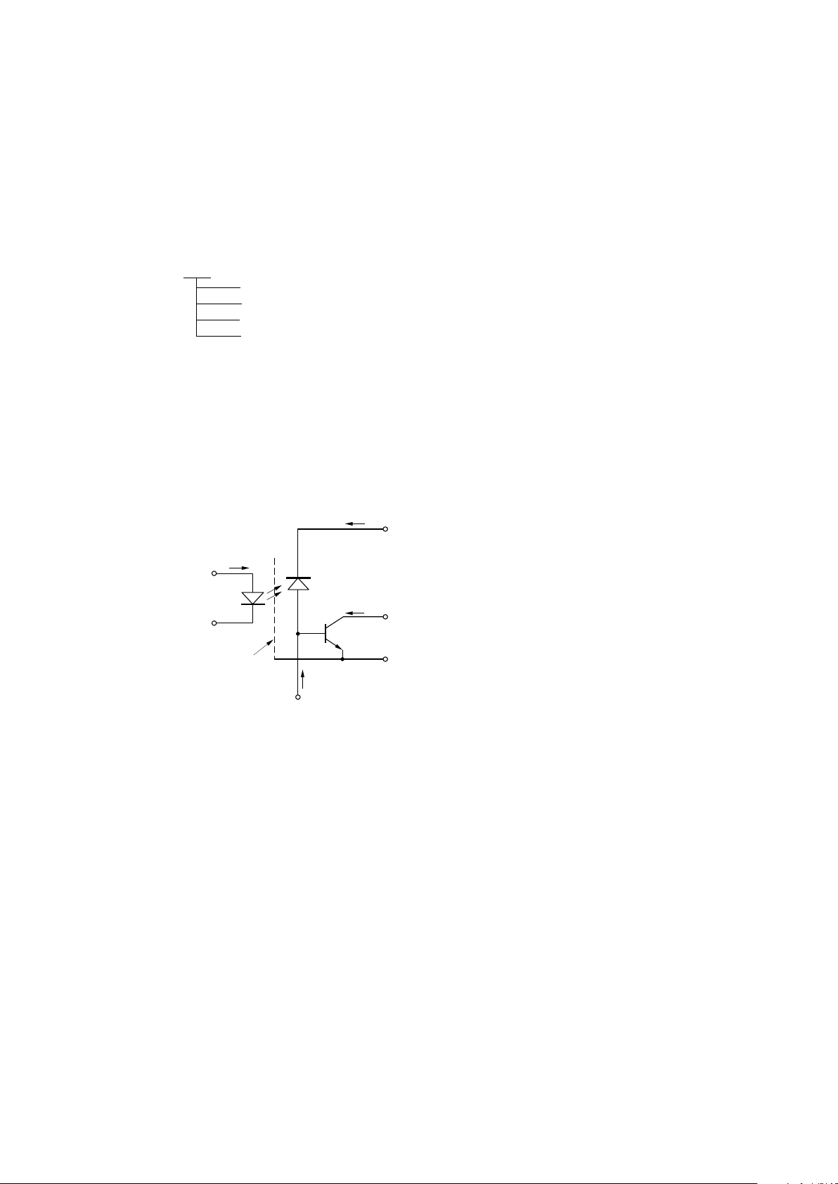
Functional Diagram
6N135/6
HCNW135/6
HCNW4502/3
HCPL-0452/3
HCPL-0500/1
HCPL-4502/3
CAUTION: It is advised that normal static precautions be taken in handling and assembly of this component to
prevent damage and/or degradation which may be induced by ESD.
A 0.1 µF bypass capacitor must be connected between pins 5 and 8.
7
1
2
3
4
5
6
8
NC
ANODE
CATHODE
NC
V
CC
V
B
V
O
GND
*
* NOTE: FOR 4502/3, 0452/3,
PIN 7 IS NOT CONNECTED.
TRUTH TABLE
(POSITIVE LOGIC)
LED
ON
OFF
V
O
LOW
HIGH
5965-3605E

1-17
Selection Guide
Widebody
Minimum CMR 8-Pin DIP (300 Mil) Small-Outline SO-8 (400 Mil) Hermetic
Current Single Dual Single Dual Single Single and
dV/dt V
CM
Transfer Channel Channel Channel Channel Channel Dual Channel
(V/
µs) (V) Ratio (%) Package Package* Package Package* Package Packages*
1,000 10 7 6N135 HCPL-2530 HCPL-0500 HCPL-0530 HCNW135
19 6N136 HCPL-2531 HCPL-0501 HCPL-0531 HCNW136
HCPL-4502† HCPL-0452† HCNW4502†
15,000 1500 19 HCPL-4503† HCPL-4534 HCPL-0453† HCPL-0534 HCNW4503†
1,000 10 9 HCPL-55XX
HCPL-65XX
4N55
*Technical data for these products are on separate HP publications.
†Pin 7, transistor base, is not connected.
The 6N136, HCPL-0501, and
HCNW136 are designed for high
speed TTL/TTL applications. A
standard 16 mA TTL sink current
through the input LED will
provide enough output current
for 1 TTL load and a 5.6 kΩ pullup resistor. CTR for these devices
is 19% minimum at IF= 16 mA.
The HCPL-4502, HCPL-0452,
and HCNW4502 provide the
electrical and switching
performance of the 6N136,
HCPL-0501, and HCNW136 with
increased ESD protection.
These single channel optocouplers are available in 8-Pin DIP,
SO-8 and Widebody package
configurations.
The 6N135, HCPL-0500, and
HCNW135 are for use in TTL/
CMOS, TTL/LSTTL or wide
bandwidth analog applications.
Current transfer ratio (CTR) for
these devices is 7% minimum at
IF= 16 mA.
The HCPL-4503, HCPL-0453,
and HCNW4503 are similar to the
HCPL-4502, HCPL-0452, and
HCNW4502 optocouplers but
have increased common mode
transient immunity of 15 kV/µs
minimum at VCM= 1500 V
guaranteed.
1-18
I
F
SHIELD
HCPL-4503/0453
HCNW4503
8
6
5
GND
V
CC
2
3
V
O
I
CC
V
F
I
O
ANODE
CATHODE
+
–
7
V
B
I
B
*
* NOTE: FOR HCPL-4502/-3, HCPL-0452/3,
HCNW4502/3, PIN 7 IS NOT CONNECTED.
Ordering Information
Specify Part Number followed by Option Number (if desired).
Example:
HCPL-4503#XXX
020 = UL 5000 V rms/1 Minute Option*
060 = VDE 0884 V
IORM
= 630 V peak Option**
300 = Gull Wing Surface Mount Option†
500 = Tape and Reel Packaging Option
Option data sheets available. Contact your Hewlett-Packard sales representative or authorized distributor for
information.
*For 6N135/6 and HCPL-4502/3 only.
**For HCPL-4503 only. Combination of Option 020 and Option 060 is not available.
†Gull wing surface mount option applies to through hole parts only.
Schematic
1-19
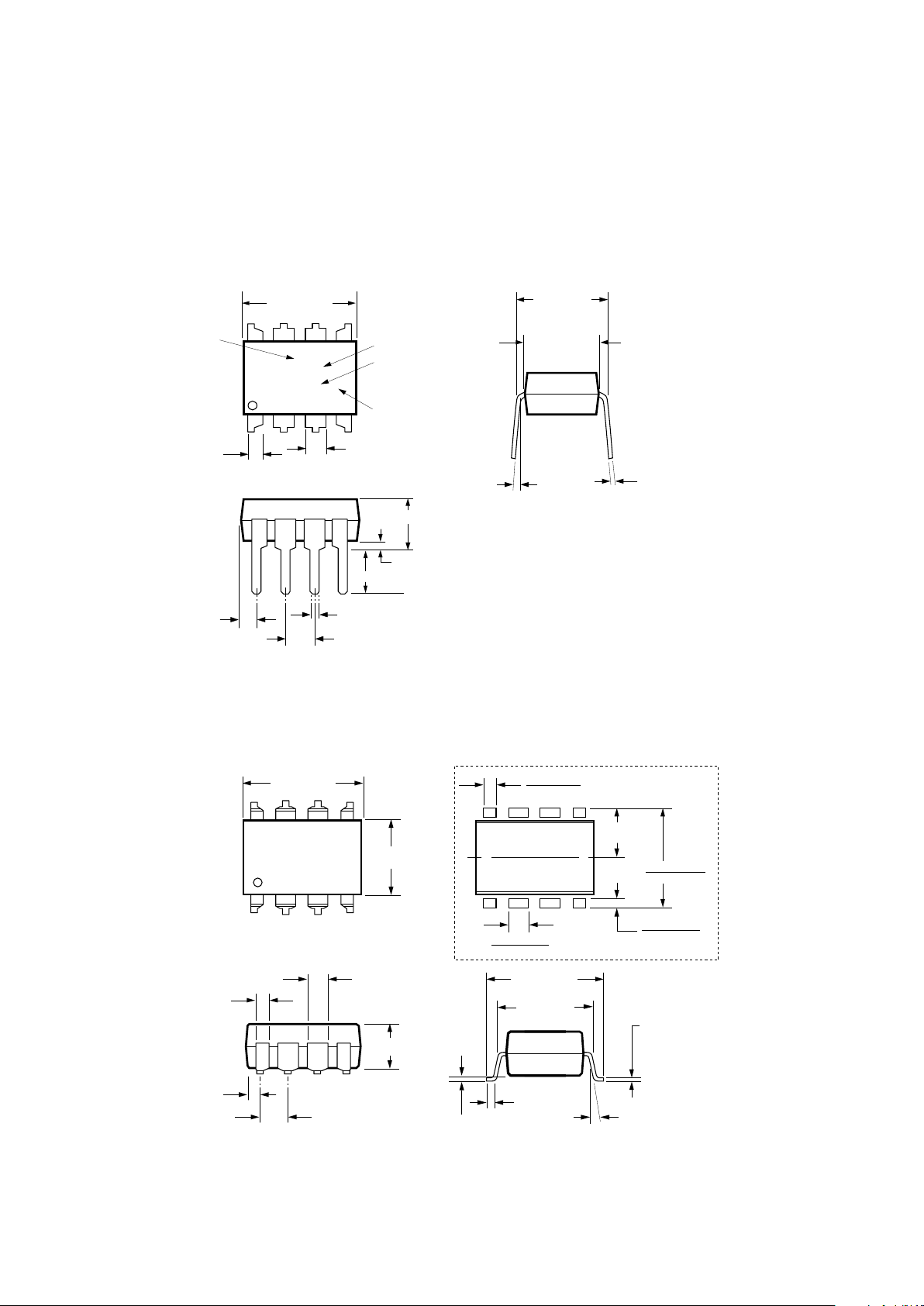
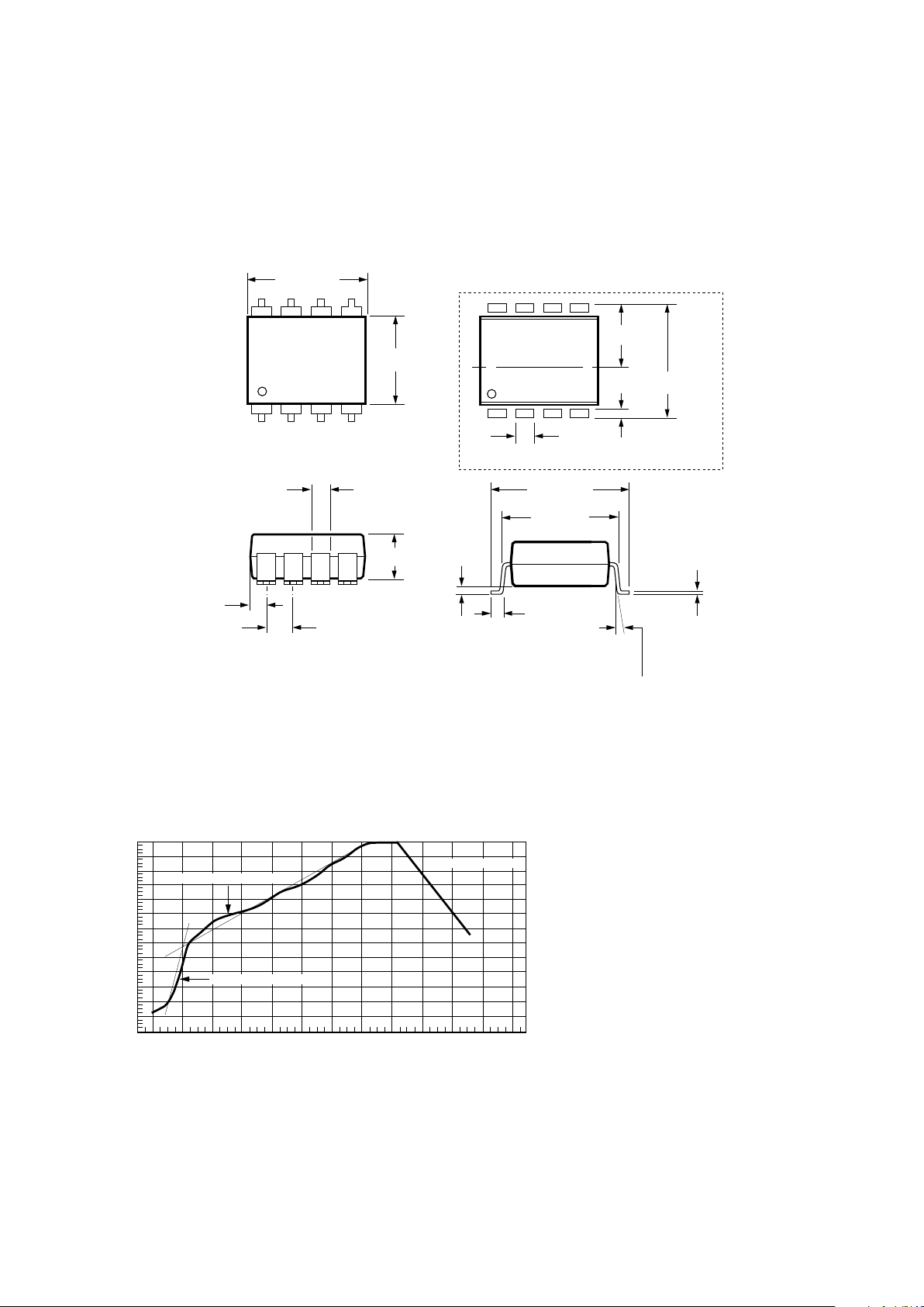
Package Outline Drawings
8-Pin DIP Package (6N135/6, HCPL-4502/3)
8-Pin DIP Package with Gull Wing Surface Mount Option 300 (6N135/6, HCPL-4502/3)
0.635 ± 0.25
(0.025 ± 0.010)
12° NOM.
9.65 ± 0.25
(0.380 ± 0.010)
0.635 ± 0.130
(0.025 ± 0.005)
7.62 ± 0.25
(0.300 ± 0.010)
5
6
7
8
4
3
2
1
9.65 ± 0.25
(0.380 ± 0.010)
6.350 ± 0.25
(0.250 ± 0.010)
1.016 (0.040)
1.194 (0.047)
1.194 (0.047)
1.778 (0.070)
9.398 (0.370)
9.906 (0.390)
4.826
(0.190)
TYP.
0.381 (0.015)
0.635 (0.025)
PAD LOCATION (FOR REFERENCE ONLY)
1.080 ± 0.320
(0.043 ± 0.013)
4.19
(0.165)
MAX.
1.780
(0.070)
MAX.
1.19
(0.047)
MAX.
2.54
(0.100)
BSC
DIMENSIONS IN MILLIMETERS (INCHES).
LEAD COPLANARITY = 0.10 mm (0.004 INCHES).
0.254
+ 0.076
- 0.051
(0.010
+ 0.003)
- 0.002)
9.65 ± 0.25
(0.380 ± 0.010)
1.78 (0.070) MAX.
1.19 (0.047) MAX.
HP XXXXZ
YYWW
DATE CODE
1.080 ± 0.320
(0.043 ± 0.013)
2.54 ± 0.25
(0.100 ± 0.010)
0.51 (0.020) MIN.
0.65 (0.025) MAX.
4.70 (0.185) MAX.
2.92 (0.115) MIN.
DIMENSIONS IN MILLIMETERS AND (INCHES).
5678
4321
5° TYP.
OPTION CODE*
UL
RECOGNITION
UR
0.254
+ 0.076
- 0.051
(0.010
+ 0.003)
- 0.002)
7.62 ± 0.25
(0.300 ± 0.010)
6.35 ± 0.25
(0.250 ± 0.010)
TYPE NUMBER
* MARKING CODE LETTER FOR OPTION NUMBERS.
"L" = OPTION 020
"V" = OPTION 060
OPTION NUMBERS 300 AND 500 NOT MARKED.
1-20
Small Outline SO-8 Package (HCPL-0500/1, HCPL-0452/3)
8-Pin Widebody DIP Package (HCNW135/6, HCNW4502/3)
XXX
YWW
8765
4321
5.842 ± 0.203
(0.236 ± 0.008)
3.937 ± 0.127
(0.155 ± 0.005)
0.381 ± 0.076
(0.016 ± 0.003)
1.270
(0.050)
BSG
5.080 ± 0.127
(0.200 ± 0.005)
3.175 ± 0.127
(0.125 ± 0.005)
1.524
(0.060)
45° X
0.432
(0.017)
0.228 ± 0.025
(0.009 ± 0.001)
TYPE NUMBER
(LAST 3 DIGITS)
DATE CODE
0.305
(0.012)
MIN.
DIMENSIONS IN MILLIMETERS (INCHES).
LEAD COPLANARITY = 0.10 mm (0.004 INCHES).
0.152 ± 0.051
(0.006 ± 0.002)
7°
5
6
7
8
4
3
2
1
11.15 ± 0.15
(0.442 ± 0.006)
1.78 ± 0.15
(0.070 ± 0.006)
5.10
(0.201)
MAX.
1.55
(0.061)
MAX.
2.54 (0.100)
TYP.
DIMENSIONS IN MILLIMETERS (INCHES).
7° TYP.
0.254
+ 0.076
- 0.0051
(0.010
+ 0.003)
- 0.002)
11.00
(0.433)
9.00 ± 0.15
(0.354 ± 0.006)
MAX.
10.16 (0.400)
TYP.
HP
HCNWXXXX
YYWW
DATE CODE
TYPE NUMBER
0.51 (0.021) MIN.
0.40 (0.016)
0.56 (0.022)
3.10 (0.122)
3.90 (0.154)
1-21
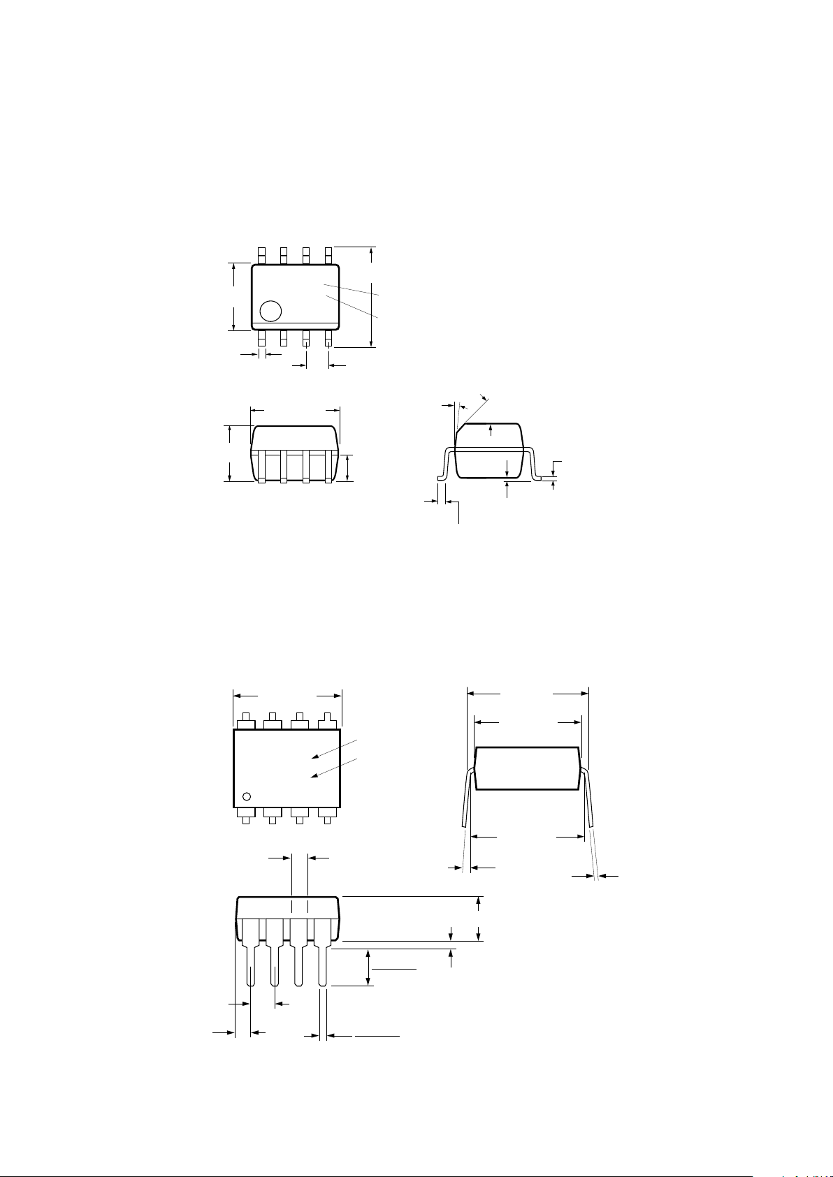
8-Pin Widebody DIP Package with Gull Wing Surface Mount Option 300 (HCNW135/6,
HCNW4502/3)
Note: Use of Non-Chlorine Activated Fluxes is Recommended.
240
∆T = 115°C, 0.3°C/SEC
0
∆T = 100°C, 1.5°C/SEC
∆T = 145°C, 1°C/SEC
TIME – MINUTES
TEMPERATURE – °C
220
200
180
160
140
120
100
80
60
40
20
0
260
123456789101112
Solder Reflow Temperature Profile (HCPL-0500/1, HCPL-0452/3, and Gull Wing
Surface Mount Option Parts)
1.00 ± 0.15
(0.039 ± 0.006)
7° NOM.
12.30 ± 0.30
(0.484 ± 0.012)
0.75 ± 0.25
(0.030 ± 0.010)
11.00
(0.433)
5
6
7
8
4
3
2
1
11.15 ± 0.15
(0.442 ± 0.006)
9.00 ± 0.15
(0.354 ± 0.006)
1.3
(0.051)
12.30 ± 0.30
(0.484 ± 0.012)
6.15
(0.242)
TYP.
0.9
(0.035)
PAD LOCATION (FOR REFERENCE ONLY)
1.78 ± 0.15
(0.070 ± 0.006)
4.00
(0.158)
MAX.
1.55
(0.061)
MAX.
2.54
(0.100)
BSC
DIMENSIONS IN MILLIMETERS (INCHES).
LEAD COPLANARITY = 0.10 mm (0.004 INCHES).
0.254
+ 0.076
- 0.0051
(0.010
+ 0.003)
- 0.002)
MAX.

1-22
Regulatory Information
The devices contained in this data
sheet have been approved by the
following organizations:
UL
Recognized under UL 1577,
Component Recognition
Program, File E55361.
CSA
Approved under CSA Component
Acceptance Notice #5, File CA
88324.
VDE
Approved according to VDE
0884/06.92 (HCNW and Option
060 devices only).
BSI
Certification according to
BS451:1994,
(BS EN60065:1994);
BS EN60950:1992
(BS7002:1992) and
EN41003:1993 for Class II
applications (HCNW devices
only).
Insulation and Safety Related Specifications
8-Pin DIP Widebody
(300 Mil) SO-8 (400 Mil)
Parameter Symbol Value Value Value Units Conditions
Minimum External L(101) 7.1 4.9 9.6 mm Measured from input terminals
Air Gap (External to output terminals, shortest
Clearance) distance through air.
Minimum External L(102) 7.4 4.8 10.0 mm Measured from input terminals
Tracking (External to output terminals, shortest
Creepage) distance path along body.
Minimum Internal 0.08 0.08 1.0 mm Through insulation distance,
Plastic Gap conductor to conductor, usually
(Internal Clearance) the direct distance between the
photoemitter and photodetector
inside the optocoupler cavity.
Minimum Internal NA NA 4.0 mm Measured from input terminals
Tracking (Internal to output terminals, along
Creepage) internal cavity.
Tracking Resistance CTI 200 200 200 Volts DIN IEC 112/VDE 0303 Part 1
(Comparative
Tracking Index)
Isolation Group IIIa IIIa IIIa Material Group
(DIN VDE 0110, 1/89, Table 1)
Option 300 - surface mount classification is Class A in accordance with CECC 00802.

1-23
VDE 0884 Insulation Related Characteristics
(HCPL-4503 OPTION 060 ONLY)
Description Symbol Characteristic Units
Installation classification per DIN VDE 0110/1.89, Table 1
for rated mains voltage ≤ 300 V rms I-IV
for rated mains voltage ≤ 450 V rms I-III
Climatic Classification 55/100/21
Pollution Degree (DIN VDE 0110/1.89) 2
Maximum Working Insulation Voltage V
IORM
630 V peak
Input to Output Test Voltage, Method b*
V
IORM
x 1.875 = VPR, 100% Production Test with tm = 1 sec, V
PR
1181 V peak
Partial Discharge < 5 pC
Input to Output Test Voltage, Method a*
V
IORM
x 1.5 = VPR, Type and sample test, V
PR
945 V peak
tm = 60 sec, Partial Discharge < 5 pC
Highest Allowable Overvoltage*
(Transient Overvoltage, t
ini
= 10 sec) V
IOTM
6000 V peak
Safety Limiting Values
(Maximum values allowed in the event of a failure,
also see Figure 9, Thermal Derating curve.)
Case Temperature T
S
175 °C
Input Current I
S,INPUT
230 mA
Output Power P
S,OUTPUT
600 mW
Insulation Resistance at TS, VIO = 500 V R
S
≥ 10
9
Ω
VDE 0884 Insulation Related Characteristics (HCNW135/6, HCNW4502/3 ONLY)
Description Symbol Characteristic Units
Installation classification per DIN VDE 0110/1.89, Table 1
for rated mains voltage ≤ 600 V rms I-IV
for rated mains voltage ≤ 1000 V rms I-III
Climatic Classification 55/85/21
Pollution Degree (DIN VDE 0110/1.89) 2
Maximum Working Insulation Voltage V
IORM
1414 V peak
Input to Output Test Voltage, Method b*
V
IORM
x 1.875 = VPR, 100% Production Test with tm = 1 sec, V
PR
2652 V peak
Partial Discharge < 5 pC
Input to Output Test Voltage, Method a*
V
IORM
x 1.5 = VPR, Type and sample test, V
PR
2121 V peak
tm = 60 sec, Partial Discharge < 5 pC
Highest Allowable Overvoltage*
(Transient Overvoltage, t
ini
= 10 sec) V
IOTM
8000 V peak
Safety Limiting Values
(Maximum values allowed in the event of a failure,
also see Figure 9, Thermal Derating curve.)
Case Temperature T
S
150 °C
Input Current I
S,INPUT
400 mA
Output Power P
S,OUTPUT
700 mW
Insulation Resistance at TS, VIO = 500 V R
S
≥ 10
9
Ω
*Refer to the front of the optocoupler section of the current catalog, under Product Safety Regulations section (VDE 0884), for a
detailed description.
Note: Isolation characteristics are guaranteed only within the safety maximum ratings which must be ensured by protective circuits in
application.

1-24
Absolute Maximum Ratings
Parameter Symbol Device Min. Max. Units Note
Storage Temperature* T
S
-55 125 °C
Operating Temperature* T
A
8-Pin DIP -55 100 °C
SO-8
Widebody -55 85
Average Forward Input Current* I
F(AVG)
25 mA 1
Peak Forward Input Current* I
F(PEAK)
8-Pin DIP 2
(50% duty cycle, 1 ms pulse width) SO-8 50 mA
(50% duty cycle, 1 ms pulse width) Widebody 40
Peak Transient Input Current* I
F(TRANS)
8-Pin DIP 1 A
(≤ 1 µs pulse width, 300 pps) SO-8
Widebody 0.1
Reverse LED Input Voltage* (Pin 3-2) V
R
8-Pin DIP 5 V
SO-8
Widebody 3
Input Power Dissipation* P
IN
8-Pin DIP 45 mW 3
SO-8
Widebody 40
Average Output Current* (Pin 6) I
O(AVG)
8mA
Peak Output Current* I
O(PEAK)
16 mA
Emitter-Base Reverse Voltage* V
EBR
5V
(Pin 5-7, except 4502/3, 0452/3)
Supply Voltage (Pin 8-5) V
CC
-0.5 30 V
Output Voltage (Pin 6-5) V
O
-0.5 20 V
Supply Voltage* (Pin 8-5) V
CC
-0.5 15 V
Output Voltage* (Pin 6-5) V
O
-0.5 15 V
Base Current* (Pin 7, except 4502/3, 0452/3) I
B
5mA
Output Power Dissipation* P
O
100 mW 4
Lead Solder Temperature*
(Through-Hole Parts Only)
1.6 mm below seating plane, 10 seconds T
LS
8-Pin DIP 260 °C
up to seating plane, 10 seconds Widebody 260 °C
Reflow Temperature Profile T
RP
SO-8 and
Option 300
*Data has been registered with JEDEC for the 6N135/6N136.
See Package Outline
Drawings section

1-25
Parameter Symbol Device Min. Typ.** Max. Units Test Conditions Fig. Note
Current CTR* 6N135 7 18 50 % TA = 25°CVO = 0.4 V IF = 16 mA, 1, 2, 5, 11
Transfer Ratio HCPL-0500 5 19 VO = 0.5 V VCC = 4.5 V 4
HCNW135
6N136 19 24 50 TA = 25°CVO = 0.4 V
HCPL-4502/3
HCPL-0501
HCPL-0452/3 15 25 VO = 0.5 V
HCNW136
HCNW4502/3
Logic Low V
OL
6N135 0.1 0.4 V TA = 25°CIO = 1.1 mA IF = 16 mA,
Output Voltage HCPL-0500 0.1 0.5 IO = 0.8 mA VCC = 4.5 V
HCNW135
6N136 0.1 0.4 TA = 25°CIO = 3.0 mA
HCPL-4502/3 0.1 0.5 IO = 2.4 mA
HCPL-0501
HCPL-0452/3
HCNW136
HCNW4502/3
Logic High IOH* 0.003 0.5 µATA = 25°CVO = VCC = 5.5 V IF = 0 mA 7
Output Current 0.01 1 TA = 25°CVO = VCC = 15 V
50
Logic Low I
CCL
50 200 µAIF = 16 mA, VO = Open, VCC = 15 V 13
Supply Current
Logic High I
CCH
* 0.02 1 µATA = 25°CIF = 0 mA, VO = Open, 13
Supply Current 2 VCC = 15 V
Input Forward VF* 8-Pin DIP 1.5 1.7 V TA = 25°CIF = 16 mA 3
Voltage SO-8 1.8
Widebody 1.45 1.68 1.85 TA = 25°CIF = 16 mA
1.35 1.95
Input Reverse BVR* 8-Pin DIP 5 V IR = 10 µA
Breakdown SO-8
Voltage Widebody 3 IR = 100 µA
Temperature ∆V
F
8-Pin DIP -1.6 mV/°CIF = 16 mA
Coefficient of ∆T
A
SO-8
Forward Voltage Widebody -1.9
Input C
IN
8-Pin DIP 60 pF f = 1 MHz, VF = 0 V
Capacitance SO-8
Widebody 90
Transistor DC h
FE
8-Pin DIP 150 VO = 5 V, IO = 3 mA
Current SO-8 130 VO = 0.4 V, IB = 20 µA
Gain Widebody 180 VO = 5 V, IO = 3 mA
160 VO = 0.4 V, IB = 20 µA
*For JEDEC registered parts.
**All typicals at TA = 25°C.
Electrical Specifications (DC)
Over recommended temperature (TA = 0°C to 70°C) unless otherwise specified. See note 13.

1-26
Parameter Sym. Device Min. Typ.** Max. Units Test Conditions Fig. Note
Propagation t
PHL
* 6N135 0.2 1.5 µsTA = 25°CRL = 4.1 kΩ 5, 6, 8, 9
HCPL-0500 2.0 11
HCNW135
6N136 0.2 0.8 T
A
= 25°CRL = 1.9 kΩ
HCPL-4502/3
HCPL-0501
HCPL-0452/3 1.0
HCNW136
HCNW4502/3
Propagation t
PLH
* 6N135 1.3 1.5 µsTA = 25°CRL = 4.1 kΩ 5, 6, 8, 9
HCPL-0500 2.0 11
HCNW135
6N136 0.6 0.8 T
A
= 25°CRL = 1.9 kΩ
HCPL-4502/3
HCPL-0501
HCPL-0452/3 1.0
HCNW136
HCNW4502/3
Common Mode |CM
H
| 6N135 1 kV/µsRL = 4.1 kΩ IF = 0 mA, TA = 25°C, 12 7, 8,
HCPL-0500 V
CM
= 10 V
p-p
9
HCNW135 C
L
= 15 pF
6N136 1 R
L
= 1.9 kΩ
HCPL-4502
HCPL-0501
HCPL-0452
HCNW4502
HCPL-4503 15 30 R
L
= 1.9 kΩ IF = 0 mA, TA = 25°C,
HCPL-0453 V
CM
= 1500 V
p-p
,
HCNW4503 C
L
= 15 pF
Common Mode |CM
L
| 6N135 1 kV/µsRL = 4.1 kΩ IF = 16 mA, TA = 25°C, 12 7, 8,
HCPL-0500 V
CM
= 10 V
p-p
9
HCNW135 C
L
= 15 pF
6N136 1 R
L
= 1.9 kΩ
HCPL-4502
HCPL-0501
HCPL-0452
HCNW4502
HCPL-4503 15 30 R
L
= 1.9 kΩ IF = 16 mA, TA = 25°C,
HCPL-0453 V
CM
= 1500 V
p-p
,
HCNW4503 C
L
= 15 pF
Bandwidth BW 6N135/6 9 MHz See Test Circuit 8, 10 10
HCPL-0500/1
HCNW135/6 11
*For JEDEC registered parts.
**All typicals at T
A
= 25°C.
Switching Specifications (AC)
Over recommended temperature (TA = 0°C to 70°C), VCC = 5 V, IF = 16 mA unless otherwise specified.
Delay Time
to Logic Low
at Output
Delay Time to
Logic High at
Output
Transient
Immunity at
Logic High
Level Output
Transient
Immunity at
Logic Low
Level Output

1-27
Package Characteristics
Over recommended temperature (TA = 0°C to 70°C) unless otherwise specified.
Parameter Sym. Device Min. Typ.* Max. Units Test Conditions Fig. Note
Input-Output V
ISO
8-Pin DIP 2500 V rms RH < 50%, 6, 14
Momentary SO-8 t = 1 min.,
Withstand TA = 25° C
Voltage**
8-Pin DIP 5000 6, 12,
(Option 020) 15
I
I-O
8-Pin DIP 1 µA 45% RH, t = 5 s, 6, 16
V
I-O
= 3 kVdc,
TA = 25° C
Input-Output R
I-O
8-Pin DIP 10
12
Ω V
I-O
= 500 Vdc 6
Resistance SO-8
Widebody 10
12
10
13
TA = 25° C
10
11
TA = 100° C
Input-Output C
I-O
8-Pin DIP 0.6 pF f = 1 MHz 6
Capacitance SO-8
Widebody 0.5 0.6
*All typicals at TA = 25°C.
**The Input-Output Momentary Withstand Voltage is a dielectric voltage rating that should not be interpreted as an input-output
continuous voltage rating. For the continuous voltage rating refer to the VDE 0884 Insulation Related Characteristics Table (if
applicable), your equipment level safety specification or HP Application Note 1074 entitled “Optocoupler Input-Output Endurance
Voltage,” publication number 5963-2203E.
Widebody 5000
Notes:
1. Derate linearly above 70°C free-air temperature at a rate of 0.8 mA/°C (8-Pin DIP).
Derate linearly above 85°C free-air temperature at a rate of 0.5 mA/°C (SO-8).
2. Derate linearly above 70°C free-air temperature at a rate of 1.6 mA/°C (8-Pin DIP).
Derate linearly above 85°C free-air temperature at a rate of 1.0 mA/°C (SO-8).
3. Derate linearly above 70°C free-air temperature at a rate of 0.9 mW/°C (8-Pin DIP).
Derate linearly above 85°C free-air temperature at a rate of 1.1 mW/°C (SO-8).
4. Derate linearly above 70°C free-air temperature at a rate of 2.0 mW/°C (8-Pin DIP).
Derate linearly above 85°C free-air temperature at a rate of 2.3 mW/°C (SO-8).
5. CURRENT TRANSFER RATIO in percent is defined as the ratio of output collector current, IO, to the forward LED input current, IF,
times 100.
6. Device considered a two-terminal device: Pins 1, 2, 3, and 4 shorted together and Pins 5, 6, 7, and 8 shorted together.
7. Common mode transient immunity in a Logic High level is the maximum tolerable (positive) dVCM/dt on the leading edge of the
common mode pulse signal, VCM, to assure that the output will remain in a Logic High state (i.e., VO > 2.0 V). Common mode
transient immunity in a Logic Low level is the maximum tolerable (negative) dVCM/dt on the trailing edge of the common mode pulse
signal, VCM, to assure that the output will remain in a Logic Low state (i.e., VO < 0.8 V).
8. The 1.9 kΩ load represents 1 TTL unit load of 1.6 mA and the 5.6 kΩ pull-up resistor.
9. The 4.1 kΩ load represents 1 LSTTL unit load of 0.36 mA and 6.1 kΩ pull-up resistor.
10. The frequency at which the ac output voltage is 3 dB below its mid-frequency value.
11. The JEDEC registration for the 6N136 specifies a minimum CTR of 15%. HP guarantees a minimum CTR of 19%.
12. See Option 020 data sheet for more information.
13. Use of a 0.1 µf bypass capacitor connected between pins 5 and 8 is recommended.
14. In accordance with UL 1577, each optocoupler is proof tested by applying an insulation test voltage ≥ 3000 V rms for 1 second
(leakage detection current limit, I
I-O
≤ 5 µA). This test is performed before the 100% Production test shown in the VDE 0884
Insulation Related Characteristics Table if applicable.
15. In accordance with UL 1577, each optocoupler is proof tested by applying an insulation test voltage ≥ 6000 V rms for 1 second
(leakage detection current limit, I
I-O
≤ 5 µA). This test is performed before the 100% Production test shown in the VDE 0884
Insulation Related Characteristics Table if applicable.
16. This rating is equally validated by an equivalent ac proof test.
6, 15

1-28
VF – FORWARD VOLTAGE – VOLTS
1000
100
10
1.0
0.1
0.01
0.001
1.2 1.3 1.4 1.5
T = 25° C
A
I
F
– FORWARD CURRENT – mA
I
F
V
F
+
–
1.81.71.6
WIDEBODY
VF – FORWARD VOLTAGE – VOLTS
100
10
0.1
0.01
1.1 1.2 1.3 1.4
I
F
– FORWARD CURRENT – mA
1.61.5
1.0
0.001
1000
I
F
V
F
+
T = 25°C
A
–
8 PIN DIP, SO-8
Figure 2. Current Transfer Ratio vs. Input Current.
Figure 3. Input Current vs. Forward Voltage.
Figure 1. DC and Pulsed Transfer Characteristics.
F
O
CC
A
0
0 1 10 100
NORMALIZED CURRENT TRANSFER RATIO
IF – INPUT CURRENT – mA
1.5
0.5
1.0
NORMALIZED
I = 16 mA
V = 0.4 V
V = 4.5 V
T = 25 °C
HCNW135/6,
HCNW4502/3
WIDEBODY
10
5
0
01020
V
O
– OUTPUT VOLTAGE – V
40 mA
35 mA
30 mA
25 mA
20 mA
15 mA
10 mA
I = 5 mA
F
T = 25°C
V = 5.0 V
A
CC
I
O
– OUTPUT CURRENT – mA
8 PIN DIP, SO-8
12
8
0
01020
V
O
– OUTPUT VOLTAGE – V
40 mA
35 mA
30 mA
25 mA
20 mA
15 mA
10 mA
I = 5 mA
F
I
O
– OUTPUT CURRENT – mA
4
16
T = 25°C
V = 5.0 V
A
CC
WIDEBODY
NORMALIZED
I = 16 mA
V = 0.4 V
V = 5 V
T = 25°C
F
O
CC
A
6N135, HCPL-0500
1.5
1.0
0.5
0.1
0 1 10 100
NORMALIZED CURRENT TRANSFER RATIO
IF – INPUT CURRENT – mA
6N136, HCPL-4502/3
HCPL-0501/0452/0453
8 PIN DIP, SO-8

1-29
3.0
2.0
1.0
0.1
4
0.6
0.4
321
0.2
8765910
0.8
R
L
– LOAD RESISTANCE – (kΩ)
t
PLH
t
PHL
V = 5.0 V
T = 25 °C
CC
I = 10 mA
I = 16 mA
F
t
P
– PROPAGATION DELAY – µs
F
A
8 PIN DIP, SO-8
RL – LOAD RESISTANCE – (kΩ)
t
P
– PROPAGATION DELAY – µs
10.0
6.0
4.0
1.0
0.1
10 40 100
0.6
0.4
4
V = 5.0 V
T = 25 °C
A
CC
I = 10 mA
I = 16 mA
F
t
21
0.2
PLH
PHL
t
t
WIDEBODY
Figure 6. Propagation Delay Time vs. Load Resistance.
Figure 5. Propagation Delay vs. Temperature.
Figure 4. Current Transfer Ratio vs. Temperature.
1.1
1.0
0.9
0.8
0.7
0.6
-60 -20 0 80
NORMALIZED CURRENT TRANSFER RATIO
TA – TEMPERATURE – °C
F
CC
A
6N135, HCPL-0500
6N136, HCPL-4502/3
HCPL-0501, 0452, 0453
8 PIN DIP, SO-8
-40 20 40 60 100
O
NORMALIZED
I = 16 mA
V = 0.4 V
V = 5 V
T = 25°C
1.1
1.0
0.9
0.8
0.7
0.6
-60 -20
20
60
100
NORMALIZED CURRENT TRANSFER RATIO
TA – TEMPERATURE – °C
0.5
80
40
0
-40
0.4
WIDEBODY
HCNW135/6,
HCNW4502/3
F
CC
A
O
NORMALIZED
I = 16 mA
V = 0.4 V
V = 5 V
T = 25°C
1000
600
400
200
0
-60 -20
20 60 100
T - TEMPERATURE - °C
A
t - PROPAGATION DELAY - ns
P
tt
800
-40
04080
HCNW136 (R = 1.9 kΩ)
HCNW4502/3
I = 16 mA, V = 5.0 V
FCC
HCNW135 (R = 4.1 kΩ)
L
L
PHLPLH
WIDEBODY
6N136, HCPL-0501
HCPL-4502/3 (R = 1.9 kΩ)
HCPL-0452/3
2000
1500
1000
500
0
-60 -20
20 60 100
T – TEMPERATURE – °C
A
t – PROPAGATION DELAY – ns
P
t
PHL
t
PLH
I = 16 mA, V = 5.0 V
F
CC
6N135, HCPL-0500 (R = 4.1 kΩ)
L
L
8 PIN DIP, SO-8

1-30
OUTPUT POWER – P
S
, INPUT CURRENT – I
S
0
0
TS – CASE TEMPERATURE – °C
20050
400
12525 75 100 150
600
800
200
100
300
500
700
PS (mW)
I
S
(mA)
175
HCPL-4503 OPTION 060
OUTPUT POWER – P
S
, INPUT CURRENT – I
S
0
0
TS – CASE TEMPERATURE – °C
175
1000
50
400
12525 75 100 150
600
800
200
100
300
500
700
900
PS (mW)
I
S
(mA)
HCNW135/6, HCNW4502/3
∆
I
F
∆ I
O
– SMALL SIGNAL CURRENT TRANSFER RATIO
0
0.10
0.20
0.30
0
I
F
– QUIESCENT INPUT CURRENT – mA
25
16
4 8 12 20
TA = 25°C, RL = 100 Ω, VCC = 5 V
8 PIN DIP, SO-8
Figure 9. Thermal Derating Curve, Dependence of Safety Limiting Value with Case Temperature per VDE 0884.
Figure 8. Small-Signal Current Transfer Ratio vs. Quiescent Input Current.
Figure 7. Logic High Output Current vs. Temperature.
TA – TEMPERATURE – °C
I = 0
V = V = 5.0 V
CCO
F
-50 -25 0 +25 +50 +75 +100
10
+4
10
-2
10
-1
10
0
10
+1
10
+2
10
+3
I
OH
– LOGIC HIGH OUTPUT CURRENT – nA
-75
8 PIN DIP, SO-8
I
OH
– LOGIC HIGH OUTPUT CURRENT – nA
TA – TEMPERATURE – °C
-60 -20 0 20 40 100
10
0
10
+1
10
+2
10
+3
-40 8060
I = 0
V = V = 15 V
CCO
F
WIDEBODY
0
0.10
0.30
0 4 8 12 16 25
0.20
0.40
20
0.50
∆ IF∆ I
O
– SMALL SIGNAL CURRENT TRANSFER RATIO
IF – QUIESCENT INPUT CURRENT – mA
TA = 25°C, RL = 100 Ω, VCC = 5 V
WIDEBODY

1-31
7
1
2
3
4
5
6
8
+12 V
0.1 µF
V
FF
47 µF
51 Ω
2.1 KΩ
100 Ω
1 KΩ
1N4150
22 Ω
R
T
Q
1
TRIM FOR
UNITY GAIN
1.2 KΩ
15 KΩ
9.1 KΩ
0.1 µF
100 Ω
Q
2
Q
3
470 Ω
+12 V
0.1 µF
(1 MΩ 12 pF
TEST INPUT)
p-p
TYPICAL LINEARITY = ± 3% AT V = 1 V
TYPICAL SNR = 50dB
TYPICAL R = 375 Ω
TYPICAL V dc = 3.8 V
TYPICAL I = 9 mA
IN
T
O
F
12
3
Q , Q , Q : 2N3904
V
O
6N135/6, HCPL-0500/1
Figure 10. Frequency Response.
0.1 1.0 10 100
-20
-15
-10
-5
0
+5
T
A
= 25 °C
f - FREQUENCY - MHz
NORMALIZED RESPONSE - dB
6N135/6, HCPL-0500/1
HCNW135/6
HCNW135/6

1-32
Figure 12. Test Circuit for Transient Immunity and Typical Waveforms.
Figure 11. Switching Test Circuit.
V
O
PULSE
GEN.
Z = 50 Ω
t = 5 ns
O
r
I MONITOR
F
I
F
0.1µF
L
R
C
L
= 1.5 µF
R
M
0
t
PHL
t
PLH
O
V
I
F
OL
V
1.5 V
+5 V
1
2
3
4
8
7
6
5
1.5 V
5 V
10% DUTY CYCLE
1/f < 100 µS
*
* PIN 7 UNCONNECTED IN HCPL-4502/3,
HCPL-0452/3, HCNW4502/3
O
V
5 V
OL
V
O
V
0 V
10%
90% 90%
10%
SWITCH AT A: I = 0 mA
F
SWITCH AT B: I = 16 mA
F
CM
V
t
r
t
f
7
1
2
3
4
5
6
8
V
O
0.1 µF
L
R
+5 V
PULSE GEN.
V
CM
+
–
V
I
F
*
A
B
FF
*PIN 7 UNCONNECTED IN HCPL-4502/3, HCPL-0542/3, HCNW4502/3
 Loading...