

Page 1
CHASSIS
SERVICE MANUAL
SPECIFICATIONS
G1W
N.Hemisphere Model
Chassis No. SCC-L34E-A
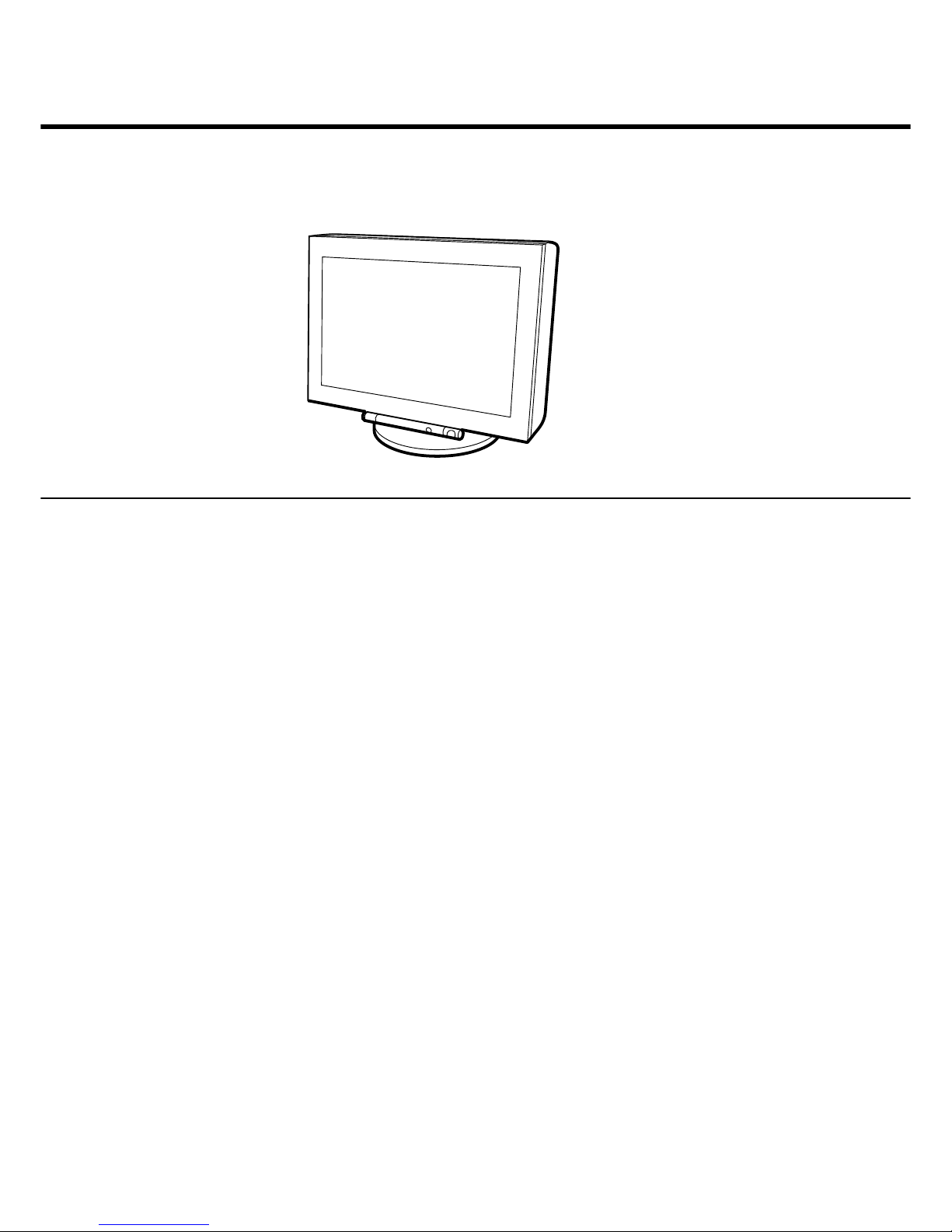
24-inch Color Monitor
GDM-FW9012
HP
()
CRT 0.23 – 0.27 mm aperture grille pitch
24 inches measured diagonally
90-degree deflection
FD Trinitron
Viewable image size Approx. 482.1 × 308.2 mm (w/h)
(19 × 12
1
/4 inches)
22.5" viewing image
Resolution Maximum (16:10)
Horizontal: 2304 dots
Vertical: 1440 lines
Maximum (4:3)
Horizontal: 2048 dots
Vertical: 1536 lines
Recommended (16:10)
Horizontal: 1920 dots
Vertical: 1200 lines
Input signal levels Video signal
Analog RGB: 0.700 Vp-p
(positive), 75 Ω
SYNC signal
H/V separate or composite sync:
TTL 2 k Ω , Polarity free
Sync on Green: 0.3 Vp-p
(negative)
Standard image area 16:10
Approx. 474 × 296 mm (w/h)
(18
3
/
4
×
11
3
/
4
inches)
4:3
Approx. 395 × 296 mm (w/h)
(15
5
/
8
×
11
3
/
4
inches)
5:4
Approx. 370 × 296 mm (w/h)
(14
5
/
8
×
11
3
/
4
inches)
()
Deflection frequency* Horizontal: 30 to 121 kHz
Vertical: 48 to 160 Hz
AC input voltage/current 100 to 240 V, 50/60 Hz, 2.2 – 1.2 A
Power consumption Approx. 160 W (with no USB devices
connected)
Operating temperature 10˚C to 40˚C
Dimensions
Approx. 571.5 × 500 ×522.5
mm(w/h/
d)
(22
1
/
2
×
19
3
/
4
×
20
5
/
8
inches)
Mass Approx. 42 kg (92 lb 10 oz)
Plug and Play DDC1/DDC2B/DDC2Bi, GTF**
Supplied accessories • Power cord (1)
• Video signal cable (1)
• USB cable (1)
• Exclusive Power Mac G3/G4
adapter (1)
• Warranty card (1)
• Notes on cleaning the screen’s
surface (1)
• This instruction manual (1)
* Recommended horizontal and vertical timing condition
• Horizontal sync width duty should be more than 4.8% of
total horizontal time or 0.8 µs, whichever is larger.
• Horizontal blanking width should be more than 2.3 µsec.
• Vertical blanking width should be more than 450 µsec.
** If the input signal is Generalized Timing Formula (GTF)
compliant, the GTF feature of the monitor will automatically
provide an optimal image for the screen.
Design and specifications are subject to change without notice.
Page 2
GDM-FW9012(E) 2
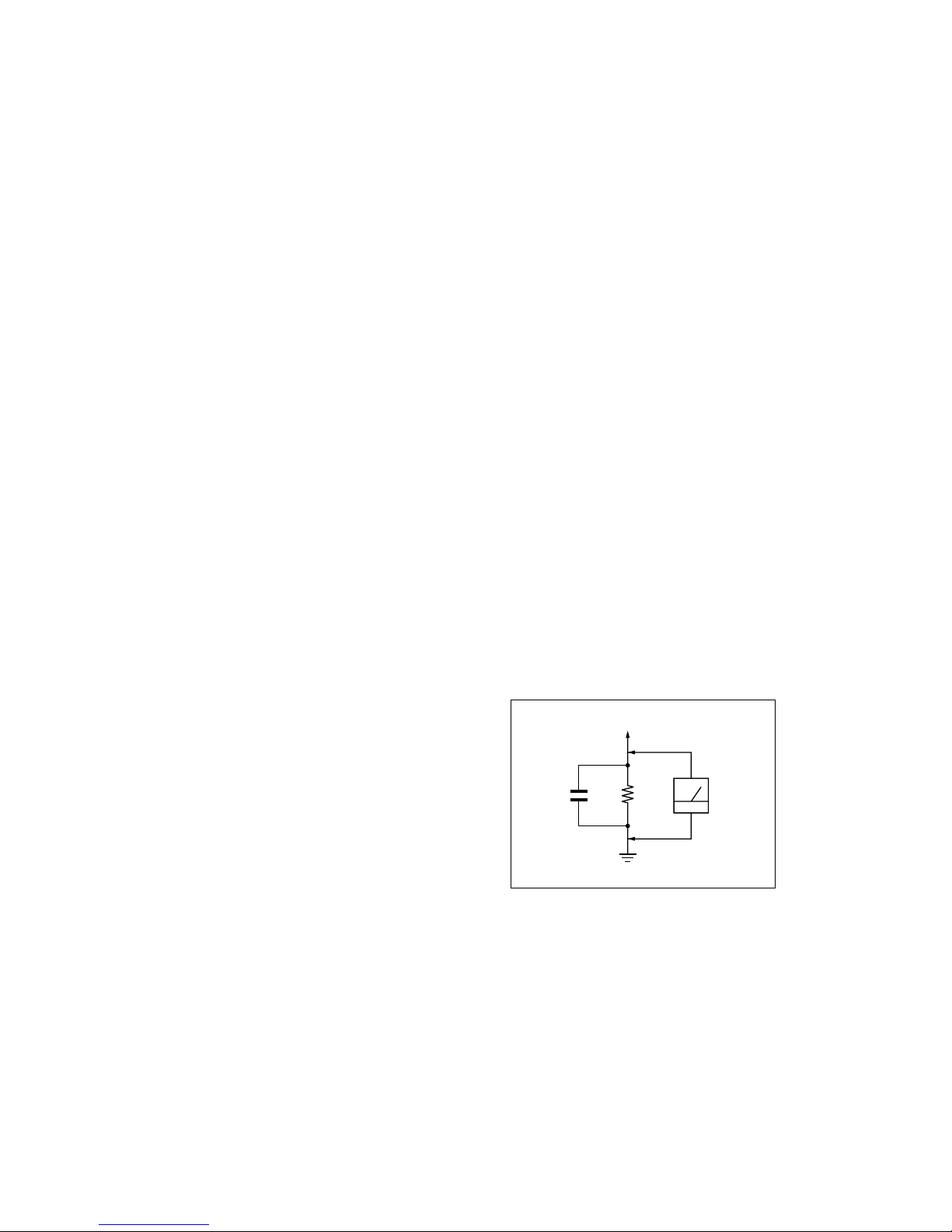
LEAKAGE TEST
The AC leakage from any exposed metal part to earth ground and from all
exposed metal parts to any exposed metal part having a return to chassis,
must not exceed 0.5 mA (500 microamperes).
Leakage current can be measured by any one of three methods.
1. A commercial leakage tester, such as the Simpson 229 or RCA WT540A. Follow the manufacturers’ instructions to use these instruments.
2. A battery-operated AC milliammeter. The Data Precision 245 digital
multimeter is suitable for this job.
3. Measuring the voltage drop across a resistor by means of a VOM or
battery-operated AC voltmeter. The “limit” indication is 0.75 V, so
analog meters must have an accurate low-voltage scale. The Simpson 250
and Sanwa SH-63Trd are examples of a passive VOMs that are suitable.
Nearly all battery operated digital multimeters that have a 2 V AC range
are suitable. (See Fig. A)
After correcting the original service problem, perform the following safety
checks before releasing the set to the customer:
1. Check the area of your repair for unsoldered or poorly-soldered
connections. Check the entire board surface for solder splashes and
bridges.
2. Check the interboard wiring to ensure that no wires are “pinched” or
contact high-wattage resistors.
3. Check that all control knobs, shields, covers, ground straps, and
mounting hardware have been replaced. Be absolutely certain that you
have replaced all the insulators.
4. Look for unauthorized replacement parts, particularly transistors, that
were installed during a previous repair. Point them out to the customer
and recommend their replacement.
5. Look for parts which, though functioning, show obvious signs of
deterioration. Point them out to the customer and recommend their
replacement.
6. Check the line cords for cracks and abrasion. Recommend the
replacement of any such line cord to the customer.
7. Check the B+ and HV to see if they are specified values. Make sure your
instruments are accurate; be suspicious of your HV meter if sets always
have low HV.
8. Check the antenna terminals, metal trim, “metallized” knobs, screws, and
all other exposed metal parts for AC Leakage. Check leakage as
described right.
Fig. A. Using an AC voltmeter to check AC leakage.
1.5 k
Ω
0.15 µF
AC
Voltmeter
(0.75 V)
To Exposed Metal
Parts on Set
Earth Ground
SAFETY CHECK-OUT
Page 3

GDM-FW9012(E) 3
WARNING!!
NEVER TURN ON THE POWER IN A CONDITION IN WHICH THE
DEGAUSS COIL HAS BEEN REMOVED.
SAFETY-RELATED COMPONENT WARNING!!
COMPONENTS IDENTIFIED BY SHADING AND MARK ! ON THE
SCHEMATIC DIAGRAMS, EXPLODED VIEWS AND IN THE
PARTS LIST ARE CRITICAL FOR SAFE OPERATION. REPLACE
THESE COMPONENTS WITH SONY PARTS WHOSE PART
NUMBERS APPEAR AS SHOWN IN THIS MANUAL OR IN
SUPPLEMENTS PUBLISHED BY SONY. CIRCUIT ADJUSTMENTS THAT ARE CRITICAL FOR SAFE OPERATION ARE
IDENTIFIED IN THIS MANUAL. FOLLOW THESE PROCEDURES
WHENEVER CRITICAL COMPONENTS ARE REPLACED OR IMPROPER OPERATION IS SUSPECTED.
AVERTISSEMENT!!
NE JAMAIS METTRE SOUS TENSION QUAND LA BOBINE DE
DEMAGNETISATION EST ENLEVÉE.
ATTENTION AUX COMPOSANTS RELATIFS À LA SÉCURITÉ!!
LES COMPOSANTS IDENTIFIÉS PAR UNE TRAME ET UNE
MARQUE ! SONT CRITIQUES POUR LA SÉCURITÉ. NE LES
REMPLACER QUE PAR UNE PIÈCE PORTANT LE NUMÉRO
SPECIFIÉ. LES RÉGLAGES DE CIRCUIT DONT L’IMPORTANCE EST
CRITIQUE POUR LA SÉCURITÉ DU FONCTIONNEMENT SONT
IDENTIFIÉS DANS LE PRÉSENT MANUEL. SUIVRE CES
PROCÉDURES LORS DE CHAQUE REMPLACEMENT DE
COMPOSANTS CRITIQUES, OU LORSQU’UN MAUVAIS
FONCTIONNEMENT EST SUSPECTÉ.
Page 4

GDM-FW9012(E) 4
POWER SAVING FUNCTION
This monitor meets the power-saving guidelines set by VESA,
E
NERGY STAR, and NUTEK. If the monitor is connected to a
computer or video graphics board that is DPMS (Display Power
Management Signaling) compliant, the monitor will automatically
reduce power consumption in three stages as shown below
.
* Figures reflect power consumption when no USB compatible
peripherals are connected to the monitor.
** “Sleep” and “deep sleep” are power saving modes defined by the
Environmental Protection Agency.
*** When your computer enters power saving mode, the input signal is
cut and NO INPUT SIGNAL appears on the screen before the
monitor enters active off mode. After a few seconds, the monitor
enters power saving mode.
Power mode Power
consumption*
! (power)
indicator
normal
operation
≤ 170 W green
1 standby ≤ 15 W green and orange
alternate
2 suspend
(sleep)**
≤ 15 W green and orange
alternate
3 active off***
(deep sleep)**
≤ 1 W orange
power off 0 W off
Page 5
GDM-FW9012(E) 5
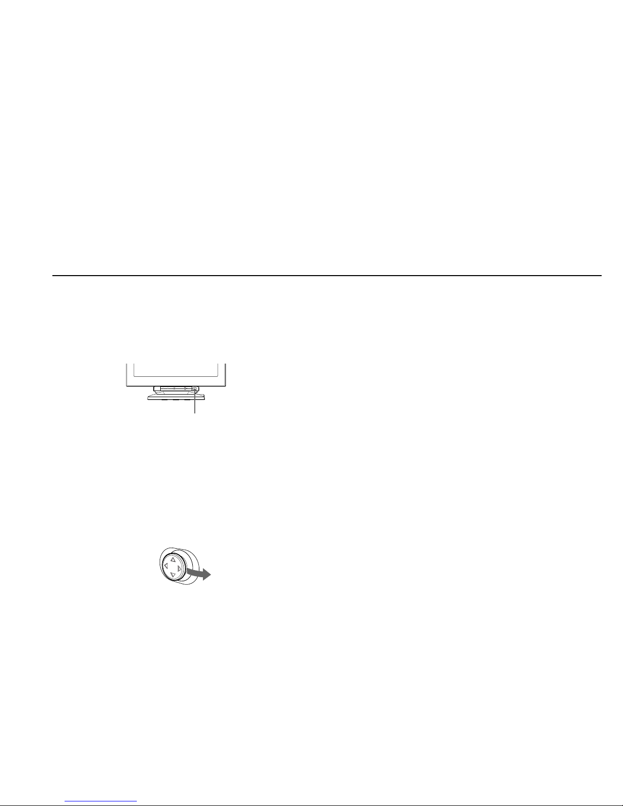
DIAGNOSIS
This monitor is equipped with a self-diagnosis function. If there is
a problem with your monitor or computer(s), the screen will go
blank and the ! (power) indicator will either light up green or
flash orange. If the ! (power) indicator is lit in orange, the
computer is in power saving mode. Try pressing any key on the
keyboard or moving the mouse.
x If the ! (power) indicator is green
1
Disconnect any plugs from the video input 1 and 2
connectors, or turn off the connected computer(s).
2
Press the ! (power) button twice to turn the monitor
off and then on.
3
Move the joystick to the right for 2 seconds before
the monitor enters power saving mode.
If all four color bars appear (white, red, green, blue), the monitor
is working properly. Reconnect the video input cables and check
the condition of your computer(s).
If the color bars do not appear, there is a potential monitor failure.
Inform your authorized Sony dealer of the monitor’s condition.
x If the ! (power) indicator is flashing orange
Press the ! (power) button twice to turn the monitor off
and then on.
If the ! (power) indicator lights up green, the monitor is working
properly.
If the ! (power) indicator is still flashing, there is a potential
monitor failure. Count the number of seconds between orange
flashes of the ! (power) indicator and inform your authorized
Sony dealer of the monitor’s condition. Be sure to note the model
name and serial number of your monitor. Also note the make and
model of your computer and graphic board.
MENU
INPUTASCRESET 21
! (power) indicator
Page 6

GDM-FW9012(E) 6
TIMING SPECIFICATION
PRIMARY MODE PRIMARY
MODE AT PRODUCTION MODE 1 MODE 2 MODE 3 MODE 4 MODE 5 MODE 6 MODE 7 MODE 8 MODE 9
RESOLUTION (HXV) 640 X 480 720 X 400 1920 X 1080 1600 X 1024 1920 X 1200 2304 X 1440 1600 X 1024 1920 X 1080 1920 X 1080
CLOCK 25.175 MHz 28.322 MHz 172.798 MHz 198.832 MHz 282.744 MHz 383.863 MHz 170.447 MHz 216.023 MHz 216.023 MHz
— HORIZONTAL —
H-FREQ 31.469 kHz 31.469 kHz 67.080 kHz 91.375 kHz 107.100 kHz 120.560 kHz 81.320 kHz 84.384 kHz 84.384 kHz
usec usec usec usec usec usec usec usec usec
H. TOTAL 31.778 31.777 14.908 10.944 9.337 8.295 12.297 11.851 11.851
H. BLK 6.356 6.355 3.796 2.897 2.546 2.292 2.910 2.963 2.963
H. FP 0.636 0.636 0.694 0.563 0.538 0.458 0.188 0.222 0.222
H. SYNC 3.813 3.813 1.204 0.885 0.736 0.667 0.939 1.000 1.000
H. BP 1.907 1.907 1.898 1.448 1.273 1.167 1.784 1.741 1.741
H. ACTIV 25.422 25.422 11.111 8.047 6.791 6.002 9.387 8.888 8.888
— VERTICAL —
V. FREQ(Hz) 59.940 Hz 70.087 Hz 60.000 Hz 85.000 Hz 85.000 Hz 80.000 Hz 76.000 Hz 72.000 Hz 72.000 Hz
lines lines lines lines lines lines lines lines lines
V. TOTAL 525 449 1118 1075 1260 1507 1070 1172 1172
V. BLK 45 49 38 51 60 67 46 92 92
V. FP 10 12 1 1 1 1 3 3 3
V. SYNC 2 2 3 3 3 3 3 3 3
V. BP 33 35 34 47 56 63 40 86 86
V. ACTIV 480 400 1080 1024 1200 1440 1024 1080 1080
— SYNC —
INT(G) NO NO NO NO NO NO NO NO NO
EXT(H/V)/POLARITY YES N/N YES N/P YES N/N YES N/N YES N/N YES N/N YES N/N YES N/N YES N/N
EXT(CS)/POLARITY NO NO NO NO NO NO NO NO NO
INT/NON INT NON INT NON INT NON INT NON INT NON INT NON INT NON INT NON INT NON INT
Page 7

GDM-FW9012(E) 7
TABLE OF CONTENTS
Section Title Page Section Title Page
1. DISASSEMBLY
1-1. Cabinet Assy Removal ......................................... 1-1
1-2. D Board Removal ................................................ 1-2
1-3. G Board Removal ................................................ 1-3
1-4. A Board and I/O Terminal Board Assy
Removal ............................................................... 1-4
1-5. S Board Removal ................................................. 1-5
1-6. N Board Removal ................................................ 1-6
1-7. Service Position .................................................... 1-7
1-8. Picture Tube Removal .......................................... 1-8
1-9. Control Block Assy Removal .............................. 1-9
1-10.J Board Removal .................................................. 1-10
1-11.US Board Removal .............................................. 1-11
1-12.Harness Location ................................................. 1-12
2. SAFETY RELATED ADJUSTMENT.......................... 2-1
3. ADJUSTMENTS ..................................................................................... 3-1
4. DIAGRAMS
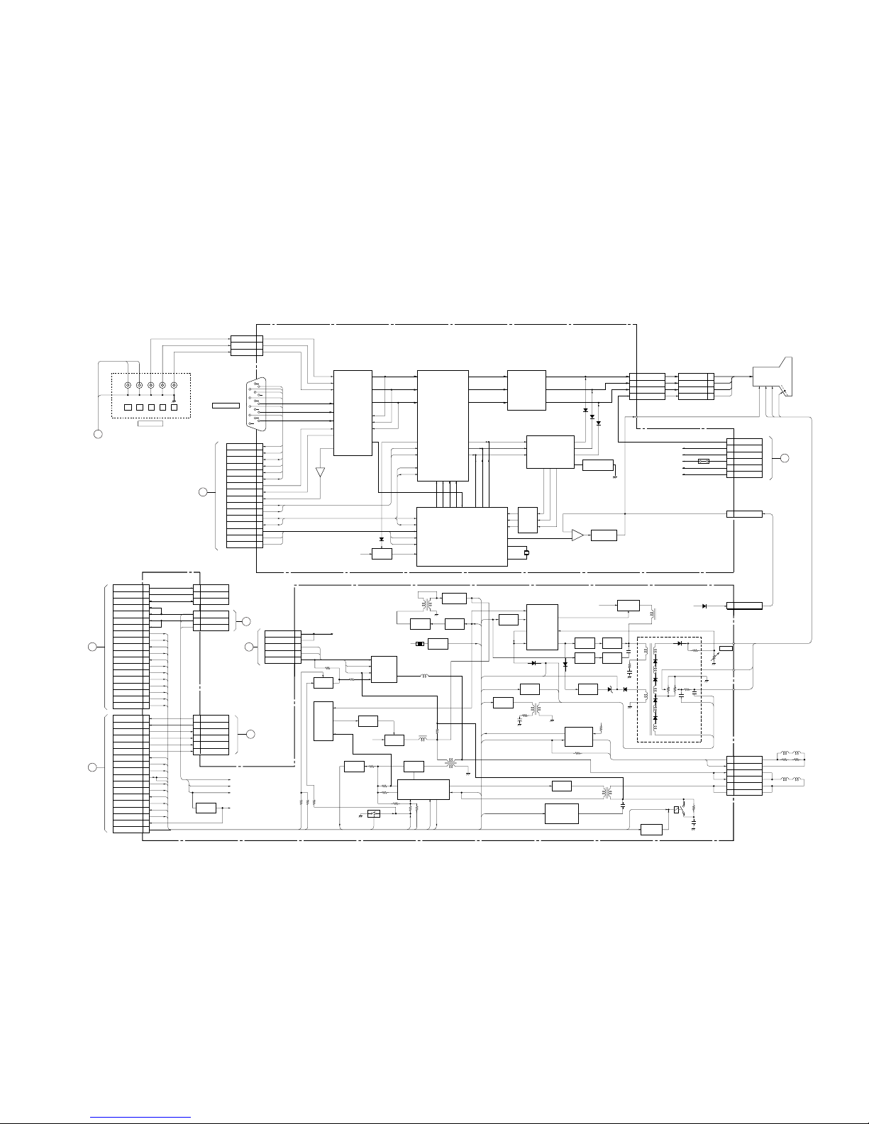
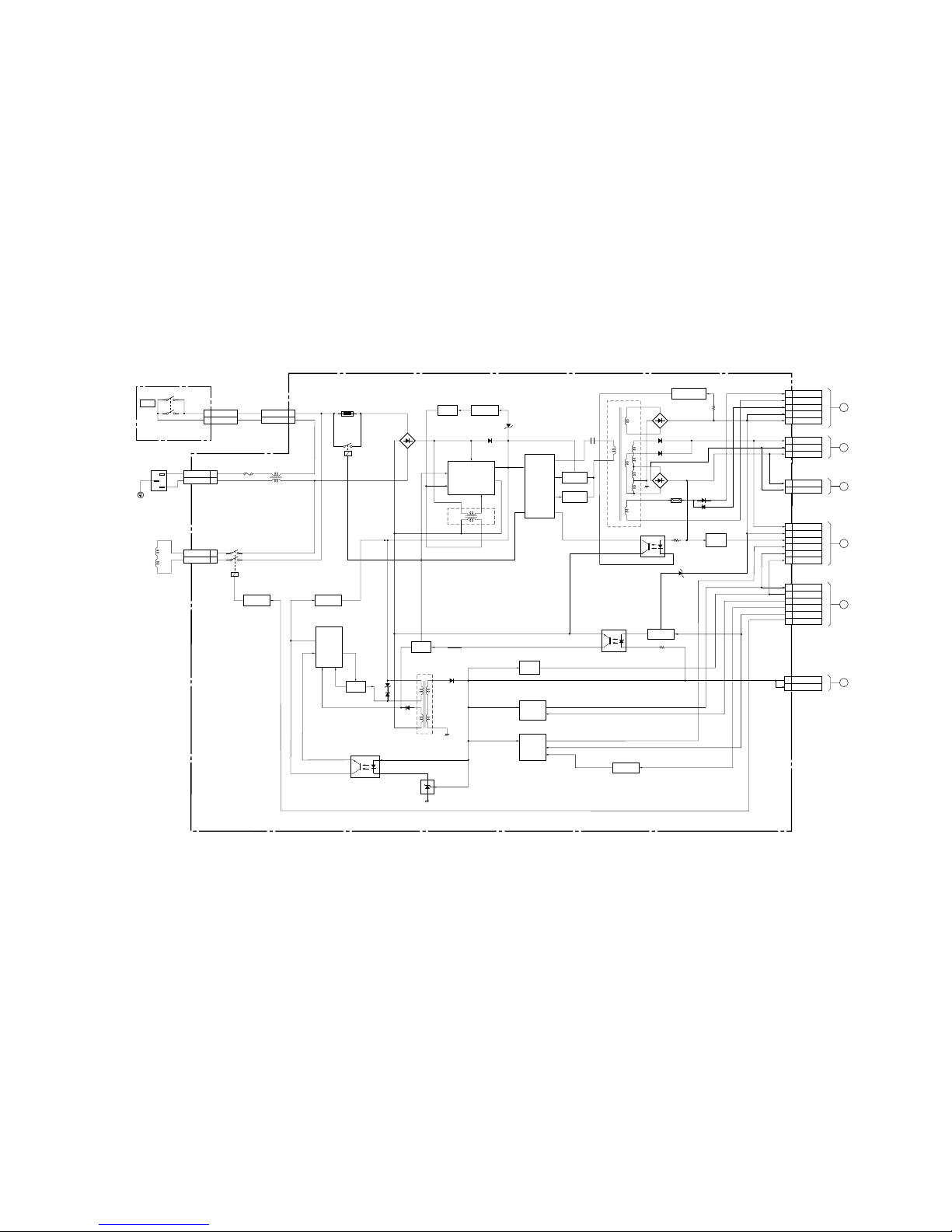
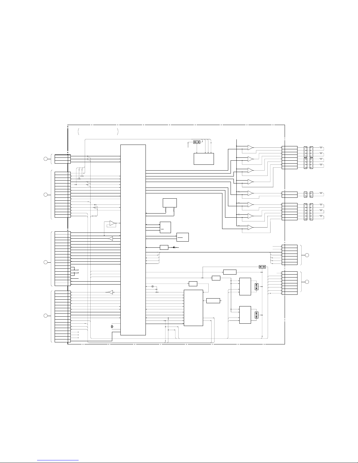
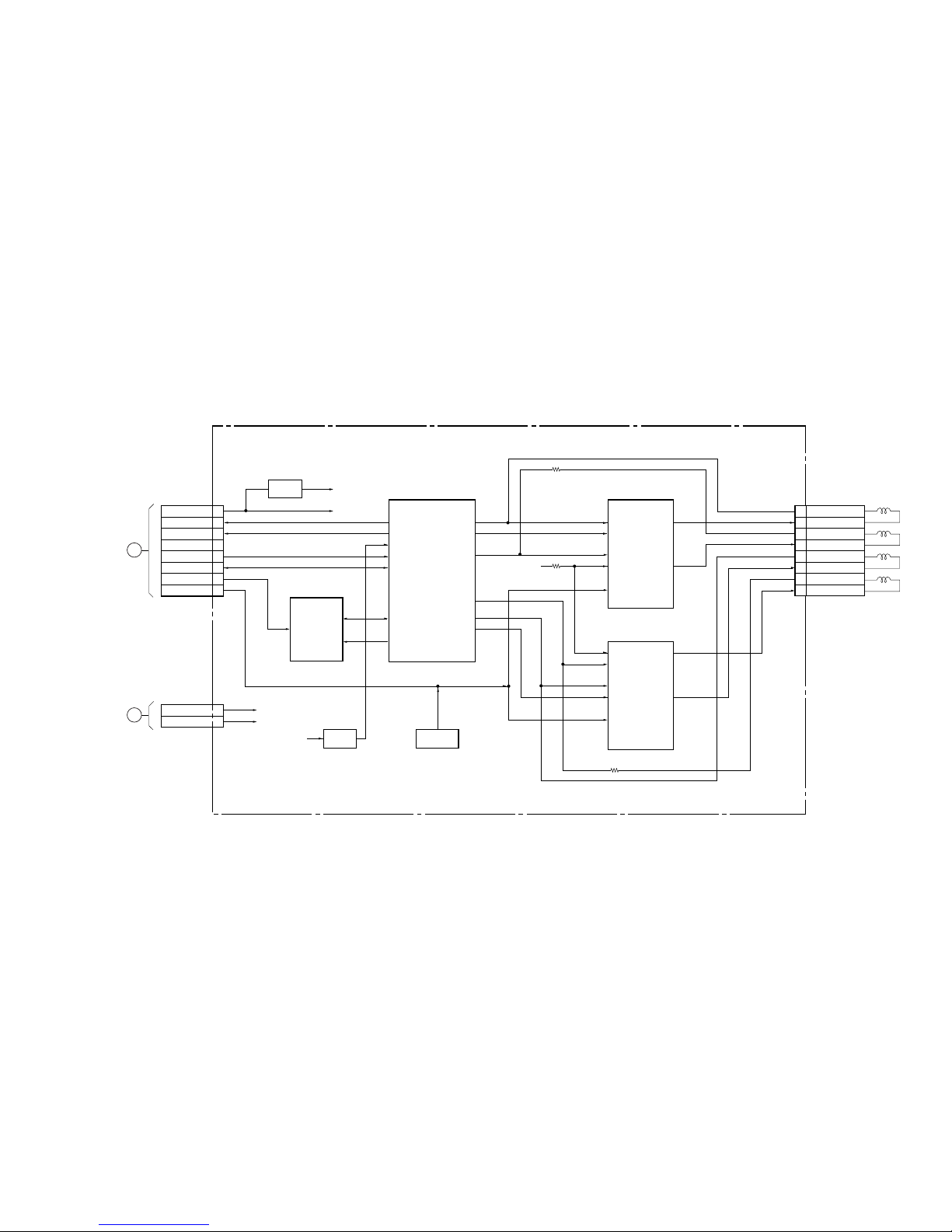
4-1. Block Diagrams .................................................... 4-1
4-2. Frame Schematic Diagram.................................... 4-6
4-3. Circuit Boards Location ........................................ 4-7
4-4. Schematic Diagrams and Printed Wiring
Boards ................................................................... 4-8
(1) Schematic Diagram of A Board .................................. 4-10
(2) Schematic Diagram of D Board .................................. 4-13
(3) Schematic Diagram of G Board .................................. 4-16
(4) Schematic Diagrams of H Boards .............................. 4-18
(5) Schematic Diagrams of J Boards ................................ 4-20
(6) Schematic Diagrams of N (a, b, c) Board ........... 4-21
(7) Schematic Diagram of S Board ................................... 4-25
(8) Schematic Diagram of US Board ................................ 4-27
4-5.Semiconductors .......................................................... 4-29
5. EXPLODED VIEWS
5-1. Chassis ................................................................. 5-1
5-2. Picture Tube ......................................................... 5-2
5-3. Packing Materials ................................................. 5-3
6. ELECTRICAL PARTS LIST ................................................. 6-1
Page 8
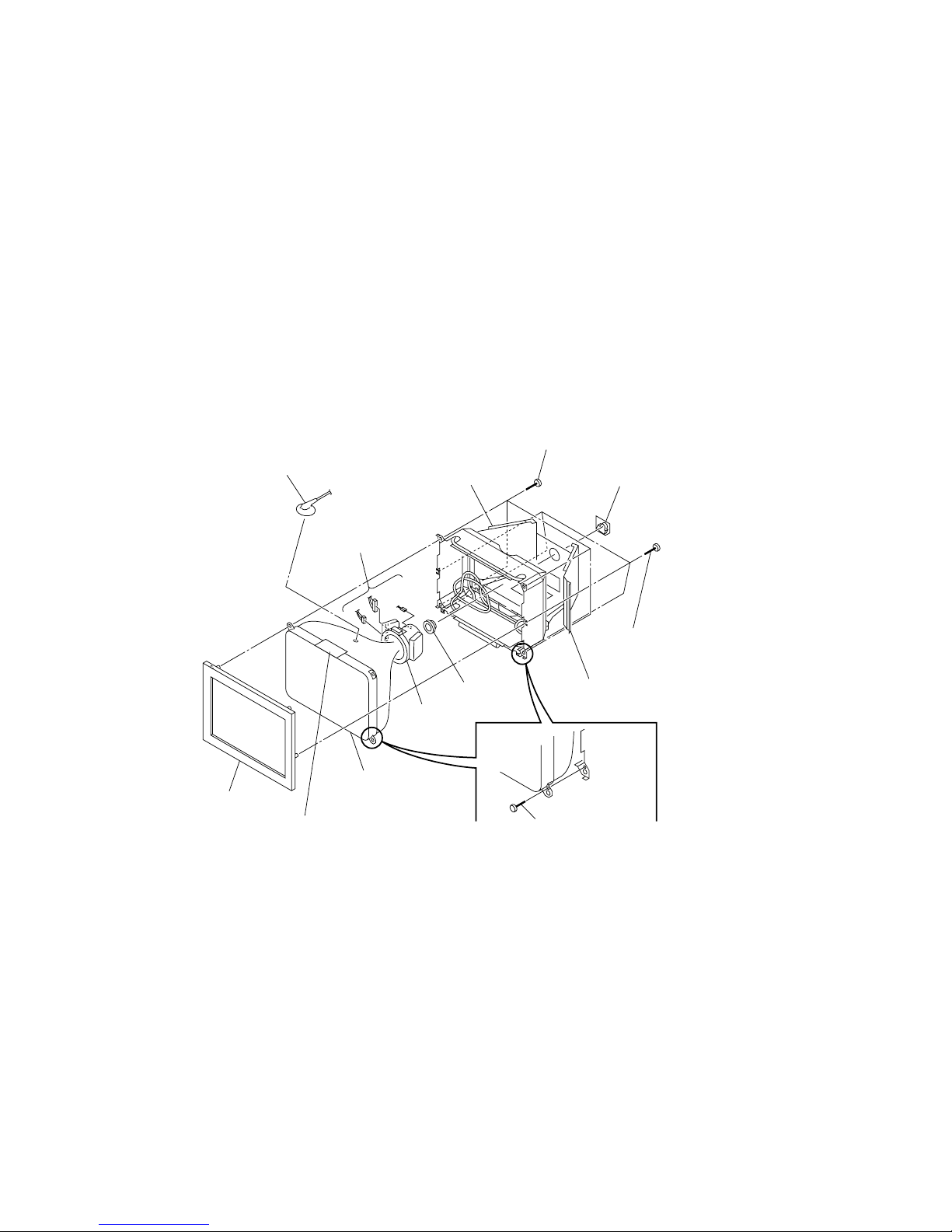
GDM-FW9012(E) 1-1
SECTION 1
DISASSEMBLY
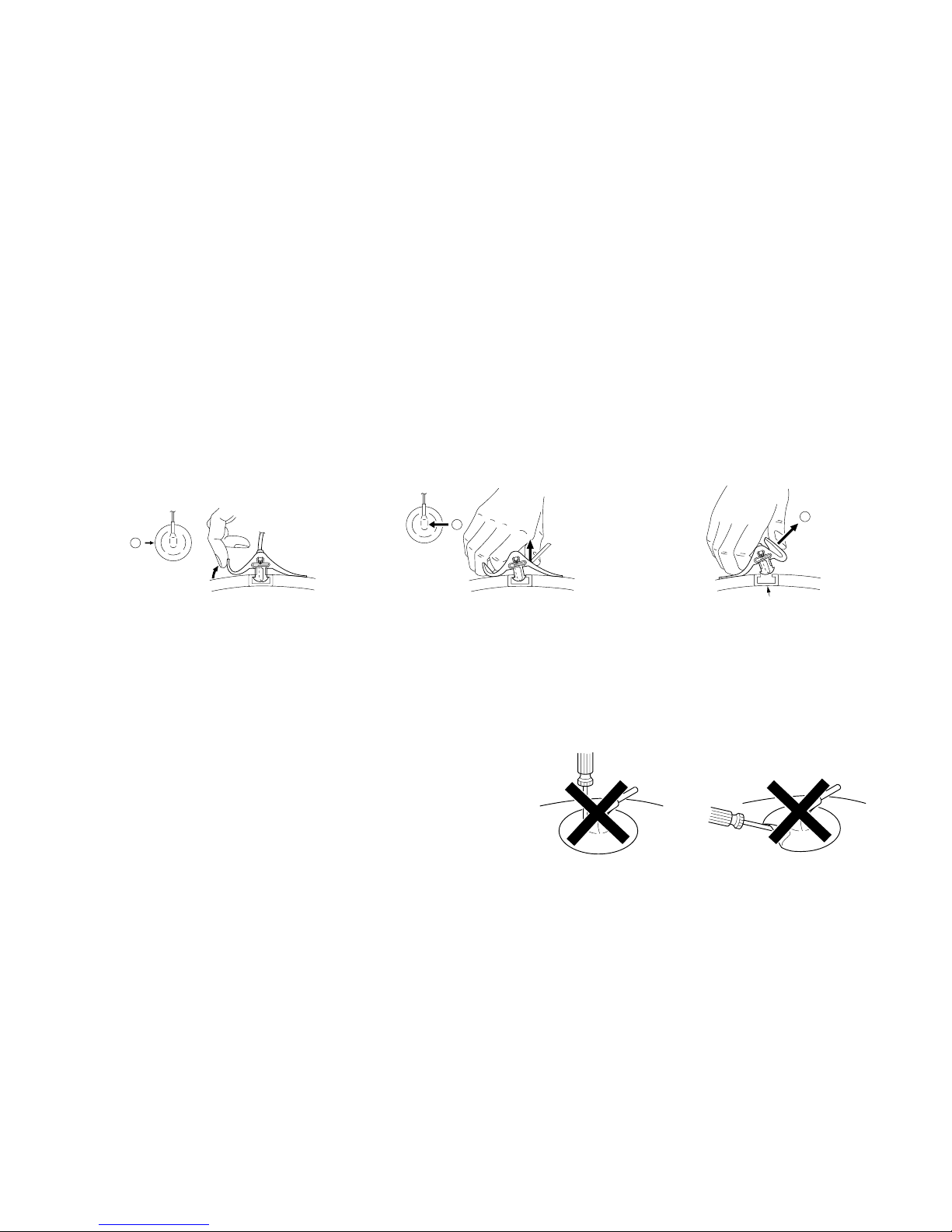
1-1. CABINET ASSEMBLY REMOVAL
1 Screw cover(L)
0 Video shield assembly
8 Top cover
6 Cabinet assembly
4 Two claws
5 Two claws
5 Two claws
2 Screw cover(R)
3 Four screws
(+ BVTP 4 x 16)
7 Four screws
(+ BVTT 4 x 8)
9 Three screws
(+ BVTT 4 x 8)
Claw
Bezel
Knock lightly cabinet
assembly in the
direction of arrow A.
A
Page 9
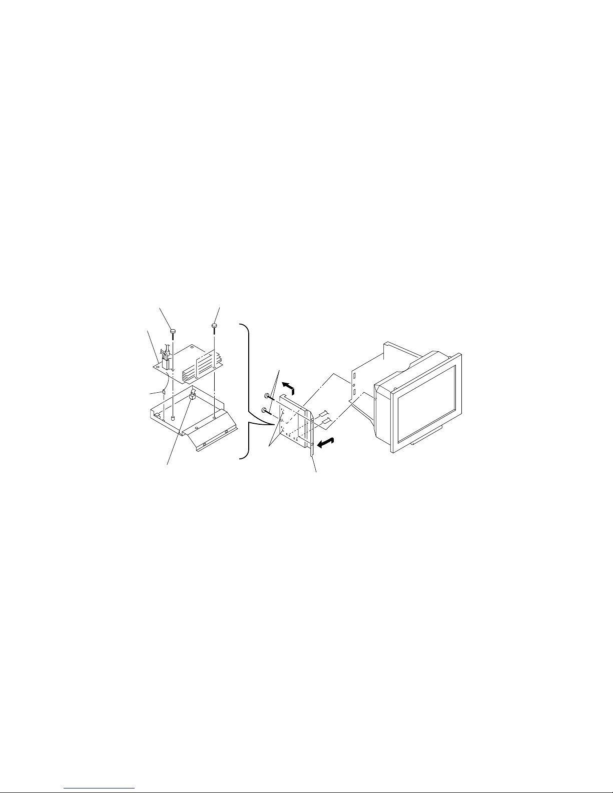
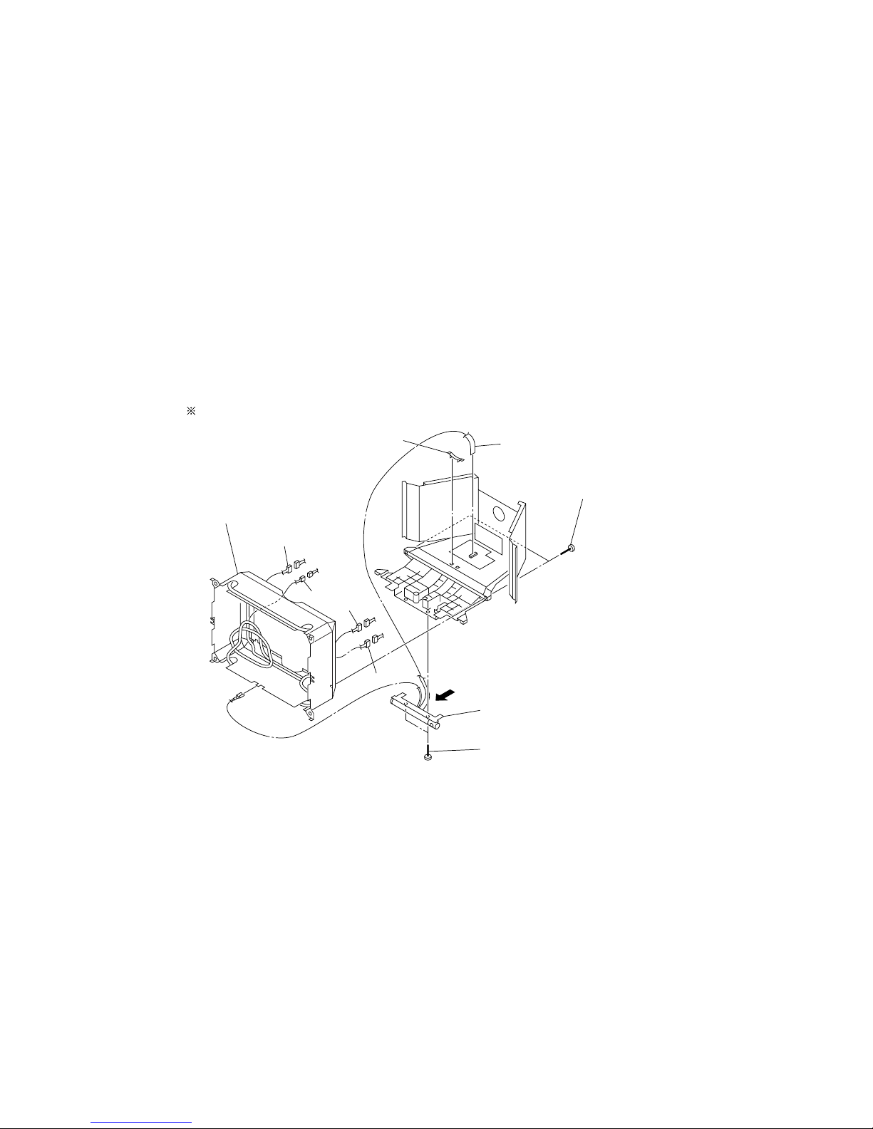
GDM-FW9012(E) 1-2
1-2. D BOARD REMOVAL
4 Two screws
(+ BVTP 3 x 12)
6 D board
Tow hooks
GND
CN504
1 Three screws
(+ BVTT 4 x 8)
5 Printed circuit board holder
3 Screw
(+ P 3.5 x 20)
2 Open the D block in the direction
of the arrow A. and remove of
the arrow B.
CN505
A
B
Page 10

GDM-FW9012(E) 1-3
1-3. G BOARD REMOVAL
Two hooks
3 Two screws
(+BVTP 3 x 8)
4 G shield
7 G board
8 Two screws
(+ KTP 3 x 8)
1 Three screws
(+ BVTT 4 x 8)
5 Screw
(+BVTP 3 x 8)
9 AC inlet (3P)
CN654
CN653
CN652
CN655
CN601
CN603
CN650
CN651
GND
GND
CN602
GND
2 Open the G block in the direction
of the arrow A. and remove of
the arrow B.
6 Two printed circuit board holders
B
A
Page 11
GDM-FW9012(E) 1-4
1-4. A BOARD,U BOARD AND I/O TERMINAL BOARD ASSY REMOVAL
4 A board (2/2)
2 Screw(M4)
(EXT TOOTH Washer)
1 Three screws
(+BVTT 4 x 8)
5 Two screws
(HD15)
6 Terminal board assembly
3 A board (1/2)
A board (1/2)
When installing terminal
bracket,be sure to apply
screw lock on 2 spots after
screws (HD15) are fixed.
A board (1/2)
Screw lock
Page 12
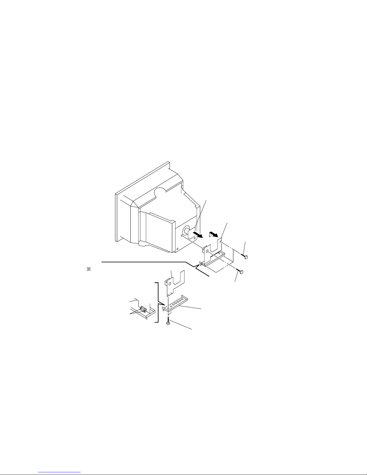
GDM-FW9012(E) 1-5
1-5. S BOARD REMOVAL
CN3003
CN3002
CN3001
2 S board
1 Screw
(+ BVTT4 x 8)
Page 13

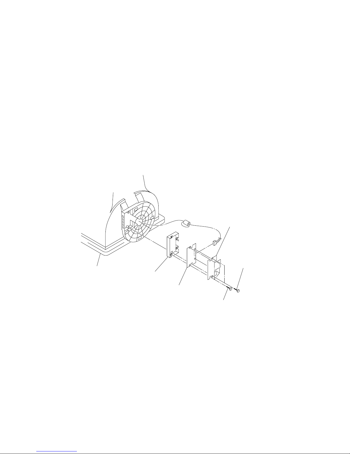
GDM-FW9012(E) 1-6
1-6. N BOARD REMOVAL
2 N board
1 Two printed circuit board holders
CN010
CN011
CN001
CN007
CN002
CN003
CN5002
CN5001
CN5003
Page 14
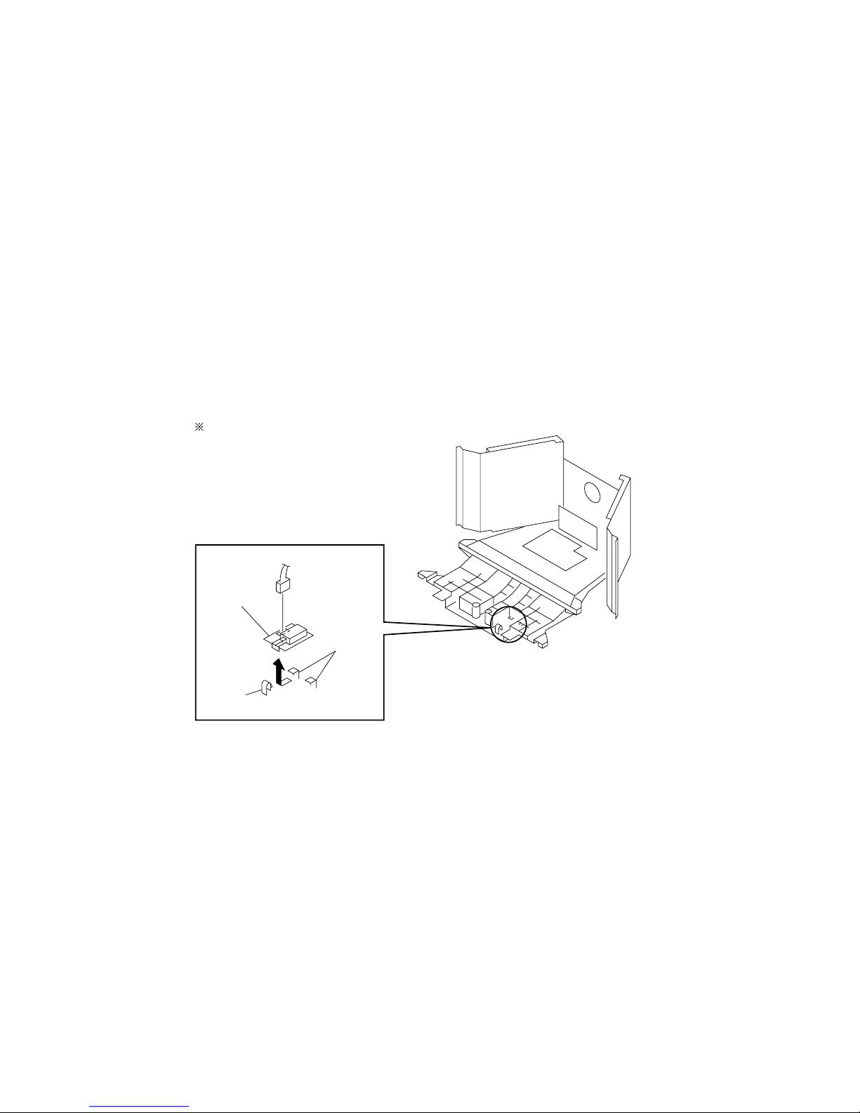
GDM-FW9012(E) 1-7
1-7. SERVICE POSITION
D board (Refer to 2-2.)
CN602
Rear shield
D,G boards
G board
(Refer to 2-3.)
AC inlet (3P)
CAUTION : SHORT
If the claw is hooked,
opening and closing
the board is impossible.
Do not try to do it by force.
If the claw is hooked,
opening and closing
the board is impossible.
Do not try to do it by force.
Page 15
GDM-FW9012(E) 1-8
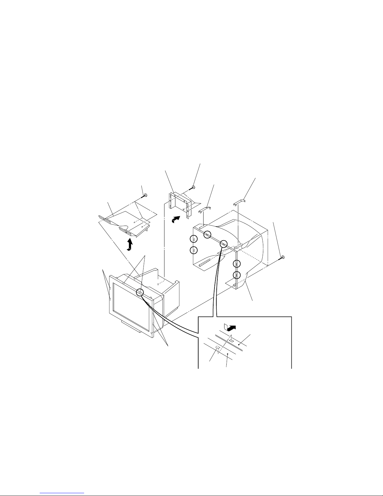
1-8. PICTURE TUBE REMOVAL
GND
P5
P6
0 Picture tube
8 Anode cap
!™ Neck assembly
!¡ Deflection yoke
5 Bezel
3 Four screws
(Tapping screw 7 + crown washer)
4 Four screws
(+BVTP 4 x 16)
9 Four screws
(+BVTT 4 x 8)
1 Open the D block.
(Refer to 2-2.)
2 Open the G block.
(Refer to 2-3.)
6 A board
7 Three connectors
PROTECTION SHEET
NOTE: When replaced the picture tube,
stick the PROTECTION SHEET
(Part No. 4-036-700-01) on the
picture tube band.
Page 16
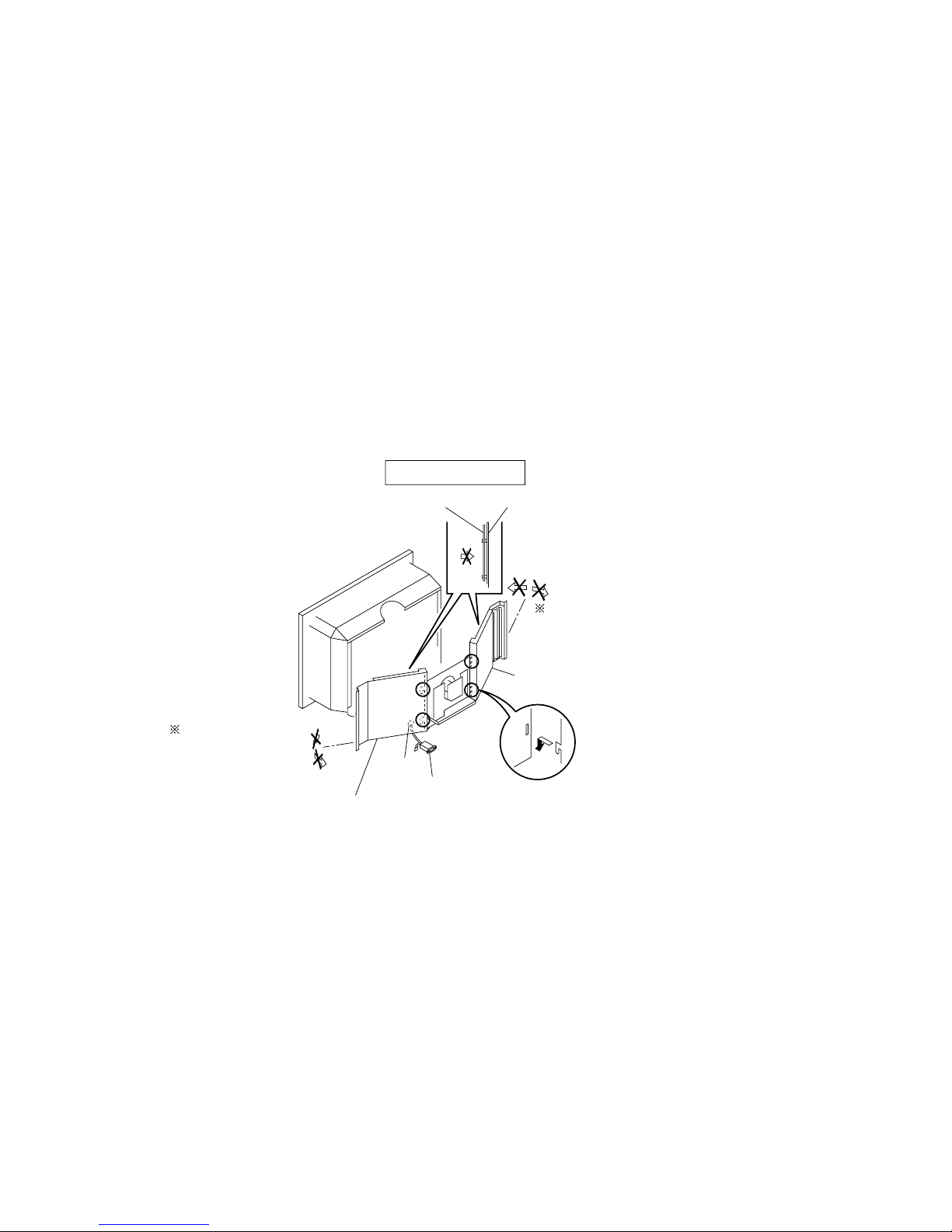
GDM-FW9012(E) 1-9
1-9. CONTROL BLOCK ASSY REMOVAL
1 Two screws
(+ BVTT 4 x 8)
3 Two screws
(
+ BVTP 3 x 12
)
4 Control block assembly
2 Picture tube shield
complete assembly
Connector(4P)
Connector(11P)
GND
Connector(2P)
Connector(4P)
Connector(2P)
Holder
Remove the picture tube.(Refer to 2-8.)
Page 17
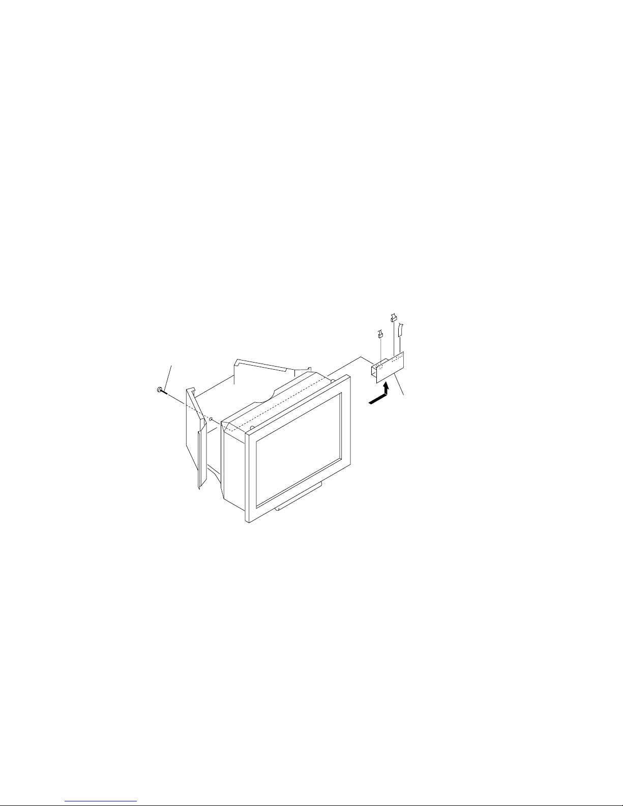
GDM-FW9012(E) 1-10
1-10. J BOARD REMOVAL
CN891
1 Claw
Two hooks
2 J board
Remove the control block assembly.(Refer to 2-9.)
Page 18
GDM-FW9012(E) 1-11
1-11. US BOARD REMOVAL
5 US board
2 Stand cover
4 USB shield
Cushion
1 Two screws
(+BVTP 3 x 12)
3 Four screws
(+BVTP 3 x 12)
CN2601
Page 19
GDM-FW9010(NE) 1-12
3 When one side of the rubber cap is
separated from the anode button, the
anode-cap can be removed by turning up
the rubber cap and pulling up it in the
direction of the arrow c.
•HOW TO HANDLE AN ANODE-CAP
1 Don’t scratch the surface of anode-caps with sharp shaped
material!
2 Don’t press the rubber hardly not to damage inside of anode-
caps!
A material fitting called as shatter-hook terminal is built in the
rubber.
3 Don’t turn the foot of rubber over hardly!
The shatter-hook terminal will stick out or damage the rubber.
•REMOVAL OF ANODE-CAP
NOTE: Short circuit the anode of the picture tube and the anode cap to the metal chassis, CRT shield or carbon painted on the CRT, after
removing the anode.
•REMOVING PROCEDURES
1 Turn up one side of the rubber cap in the
direction indicated by the arrow a.
2 Using a thumb pull up the rubber cap
firmly in the direction indicated by the
arrow b.
a
b
c
Anode Button
Page 20
GDM-FW9012(E) 2-1
Part Replaced ([)
RV901
SECTION 2
SAFETY RELATED ADJUSTMENT
When replacing or repairing the shown below table, the following
operational checks must be performed as a safety precaution against Xrays emissions from the unit.
* Confirm one minute after turning on the power.
HV ADJ
HV Regulator
Circuit Check
HV Protector
Circuit Check
Beam Current
Protector Circuit
Check
Part Replaced (])
D Board C901, R923, R924,
R929, R943, T902(FBT)
• Mounted D Board
D Board C922, C926, D912,
D915, D921, Q907,
Q908, R921, R922,
R932, R937, R939,
T902(FBT)
• Mounted D Board
D Board C921, C933, D901,
D913, R920, R928,
R930, 931, T902(FBT)
• Mounted D Board
N Board IC001, R031, R032
• Mounted N Board
a) HV Regulator Circuit Check
1) Enter black crosshatch signal (black on white background), and check
that high voltage is in the specified range.
[Specification]: 28.50 ± 0.10 kV
2) Check that the voltage of D912 cathode on the D board is 29.0 V or
more.
b) HV Protector Circuit Check
1) Enter black crosshatch signal (black on white background).
2) Apply the specified voltage to the D912 cathode on the D board, and
check that high voltage is 0.1 kV or less.
[Specification]: 34.00 + 0.00/– 0.05 V
c) Beam Current Protector Circuit Check
(1st Protector): D Board
1) Apply 4.5 V DC to CN504 0 pin on the D board, and check high
voltage value.
2) Connect constant current source to a section between T902 (FBT) qa pin
and qs pin (GND) on the D board, and check that high voltage checked in
1) lowers by 1.50 kV or more when the specified current flows to the qa
pin.
[Specification]: 2.00 + 0.00/– 0.01 mA
d) Beam Current Protector Circuit Check
(2nd Protector): D Board
1) Connect constant current source to a section between T902 (FBT) qa pin
and qs pin (GND) on the D board, and check that the voltage of CN504 0
pin becomes 0 V or less when the specified current flows to the qa pin.
[Specification]: 1.63 + 0.00/– 0.01 mA
Page 21

GDM-FW9012(E) 2-2
e) Beam Current Protector Circuit Check
: G Board
1) Apply 264 V AC.
2) Enter about 5 V to CN650 4 pin on the G board, and check that the
output voltage of CN653 2 pin is about 15 V.
3) Enter about 0 ± 0.2 V to CN650 4 pin, and check that the output
voltage of CN653 2 pin becomes 1.0 V or less.
f) Beam Current Protector Circuit Check
: N Board
1) Check that the protector operates, when the voltage of CN010 qh pin
on the N board is lowered to 0 V or less (for more than 2 seconds).
Page 22

GDM-FW9012(E) 3-1
SECTION 3
ADJUSTMENTS
Note: Hand degauss must be used on stand-by or power-off condition.
This model has an automatic earth magnetism correction function by using an earth magnetism sensor and a LCC coil. When
using a hand degauss while monitor (LCC coil) is being operated, it sometimes gets magnetized, and the system may not
work properly as a result.
•Landing Rough Adjustment
1. Enter the full white signal. (or the full black dots signal).
2. Adjust the contrast to the maximum.
3. Make the screen monogreen.
Note:Off the outputs from R ch and B ch of SG.
4. Reverse the DY, and adjust coarsely the purity magnet so that
a green raster positions in the center of screen.
5. Adjust the tilt of DY, and fix lightly with a clamp.
Note:“TILT” = “128”.
•Landing Fine Adjustment
1. Put the set inside the Helmholtz coil. (“LCC SW” = “12”)
2. Input the single green signal and set the “CONTRAST” =
“255”.
Note:After the W/B adjustment with 9300K, measure an average
of ΣIk when a full white signal is entered in the CONT
MAX/BRT CENT status. Then make adjustment so that the
specified screen can be attained after aging for 2 hours with
Ik equivalent to 30% of the average value.
3. Demagnetize the metal part of the chassis with the hand degausser and coil
degausser, and the CRT surface with the hand degausser.
Input AC 230V to AC IN, turn on and off the power to perform auto
degaussing. (Perform auto degaussing by setting “FUNCTION SW” = 1.
Return to the original value after use.)
Demagnetize the CRT surface with the hand degausser again.
Note:
(1) Hand degauss must be used on stand-by or power-off condition.
This model has an automatic earth magnetism correction function by using
an earth magnetism sensor and a LCC coil. When using a hand degauss while
monitor (LCC coil) is being operated, it sometimes gets magnetized, and the
system may not work properly as a result.
(2) Adjust in a non-magnetic field.
(3) If adjusting in a magnetic fields, add the shift from the non-magnetic field in
your estimation.
4. Attach the wobbling coil to the designated part of the CRT neck.
5. Attach the sensor of the landing adjustment unit on the CRT surface.
Page 23

GDM-FW9012(E) 3-2
6. Adjust the DY position and purity, and the DY tilt, and landing
of the center and 4 corners with the landing checker.
After adjustment, set “LCC SW” to “13”.
• Write terrestrial magnetism sensor reading VX and VY to
“LCC VX” and LCC VY” respectively. Adjust the landing by
moving “LCC NS”, “LCC LT”, “LCC LB”, “LCC RT” and
“LCC RB”. However, the register adjustment must be limited
within the following range.
“LCC NS” 128 ± 45
“LCC LT”, “LCC LB”, “LCC RT”, “LCC RB”
128 ± 40
Save the service data.
* Adjustment and measurement should be made at the points one
inch inside the fluorescent screen.
7. Tighten DY screw.
Note:Torque 22 ± 2 kg.cm (2.2 ± 0.2 Nm) auto degauss it.
8. For the up/down swing, swing the DY and insert a wedge so
that the up and down pins are equal at the top and bottom.
Adjust the H.TRP VR of DY so that the horizontal trapezoid is
equal at the left and right. Insert the wedge firmly so that the DY
does not shake.
9. Check the landing of each corner, and if it does not satisfy the
specification, adjust the landing of four corners using “LCC
LT“, “LCC LB”, “LCC RT” and “LCC RB”.
However, the register adjustment must be limited within the
following range.
“LCC NS” 128 ± 15
<Specifications>
Adjust so that the green is within the
specification given right.
4 corner adjust target : within ± 1
The red and blue must be within the
specification given right with respect to
the green.
A difference between red and blue must
be within the specification given right.
“LCC LT”, “LCC LB”, “LCC RT”, “LCC RB”
128 ± 45
After adjustment, save the service data.
10. Remove the sensor and wobbling coil.
11. Switch the signal to R.G.B., and check that each color is pure.
12. Check that the DY is not tilting, and fix the purity Mg with a white pen. Fix
wedges with RTV.
± 6 ± 6 ± 6
± 6 ± 6 ± 6
± 6 ± 6 ± 6
0 ± 30 ± 7.5 0 ± 3
0 ± 30 ± 7.5 0 ± 3
0 ± 30 ± 7.5 0 ± 3
10 10 10
10 7 10
10 10 10
(µm)
(µm)
(µm)
Page 24
GDM-FW9012(E) 3-3
Connect the communication cable of the computer to the connector located on the D board. Run the service software and then follow the instruction.
IBM AT Computer
as a Jig
*The parts above (1 and 2) are necessary for DAS adjustment.
To BUS CONNECTOR
1-690-391-21
Cord,Connection
D-sub
(9 pin [female])
mini Din
(8 pin)
1
A-1500-819-A
Interface Unit
2
Connector
Attachment
Box Unit
4 pin
•Convergence Rough Adjustment
(1) Receive an image of the white crosshatch signals (white lines
on black).
(2) Place the protrusions of the 6-fold poles magnet attached to
the CRT neck upon each other.
(3) Make rough adjustment of the H and V direction convergence
by using 4-fold poles magnet.
H-TRP
YBH
TLH
TLV
APH
XBV
YCH
XCV
Purity
4-pole magnet
6-pole magnet
2-pole magnet
* Set so that the protruding parts of the 2
magnet rings agree with each other.
Page 25
GDM-FW9012(E) 3-4
•Convergence Specification
XBVXCV
B
R
B
R
R
B
B
R
R
BBR
TLV
TLH
YBHYCH
R B
R B
B
C
A
A
0.24 mm
70kHz
70kHz >
0.24 mm
B
0.24 mm
C
0.28 mm
0.28 mm
0.32 mm
V
fH
•White Balance Adjustment Specification
1. 9300K
x = 0.283 ± 0.015
y = 0.298 ± 0.015
(All White)
2. 6500K
x = 0.313 ± 0.015
y = 0.329 ± 0.015
(All White)
3. 5000K
x = 0.346 ± 0.015
y = 0.359 ± 0.015
(All White)
•Vertical and Horizontal Position and Size
Specification
B
a
a 3.5 mm
b 3.5 mm
a
b
b
A
MODE
A
B
16 : 9
474
474
16 : 10
266
296
MODE
A
B
4 : 3
395
296
5 : 4
370
296
•Focus adjustment
Adjust the focus volume 1 and 2 for the optimum focus.
Focus 1
Focus 2
FBT
Page 26
GDM-FW9012(E) 4-1
SECTION 4
DIAGRAMS
4-1. BLOCK DIAGRAMS
18
21
19
17
16
20
12
7
6
2
4
13
14
8
9
10
DDC +5V 1
HOST GND 1
DDC SCL 1
VS1
HS/CS1
DDC SDA 1
INPUT SEL
G. SYNC DET
SYNC ON G
CLP
C. BLK
SCL
SDA
H. SYNC
V. SYNC
HFBP
B
TO N BOARD
CN001
5
3
1
35
32
29
23
21
19
17
26
27
28
11
9
7
BIN2
GIN2
RIN2
OSD R
OSD G
OSD B
OSD BLK
ROUT
GOUT
BOUT
41
38
33
2
8
12
2
6
11
ROUT
GOUT
BOUT
4
6
14
ROUT
GOUT
BOUT
RIN
GIN
BIN
RIN
GIN
BIN
R DET IN
G DET IN
B DET IN
V-DET
D/A4
D/A3
D/A2
CLP
C. BLK
SCL
SDA
BIN1
GIN1
RIN1
18
14
25
25
21
30
22
23
INPUT SW
G. DET
SYNC SEP OUT
D/A5
CLP
BLK
SCL
SDA
2
4
6
BIN2
GIN2
RIN2
CN402
IC407
CN403
CN401
HD15
5
4
3
2
1
10
15
9
14
8
13
7
12
6
11
INPUT1(HD15)
VCC KICK
Q402
IC404
OSD
5V
IC401
INPUT SELECT
IC402
RGB DRIVE
IC403
RGB AMP
4 9 13 1
18 19 20 21 15 16 17
10 11 12
17
6
514
11
12
7
7
5
3
26
25
24
4
3
5
6
7
13
14
15
ROUT
GOUT
BOUT
GND
RCI
GCI
BCI
PWM1
XT1
XT0
H. SYNC
V. SYNC
HFBP
SCL
SDA
SCL
SDA
VS
Hfly
RIN
GIN
BIN
IC406
CUTOFF AMP
X401
8MHz
G2
G2 CONT
Q406, 407, 410
IC405 (1/2)
+
-
ROUT
GOUT
BOUT
FBLK
AV
PWM2
PWM3
PWM4
B BKG
G BKG
R BKG
BUFFER
Q101,
Q201,
Q301
9
1
2
4
6
8
HEATER
STBY+5V
1W+5V
+80V
+220V
+12V
5V
5V-2
+80V
+220V
+12V
PS401 1A
CN405
G2
1
G2
CN406
5
3
1
7
KR
KG
KB
HEATER+
CN407
5
3
1
7
KR
KG
KB
HEATER+
FVFCHV
CN408
V901
PICTURE TUBE
8
E
TO G BOARD
CN652
A
(VIDEO AMP, RGB OUT)
RIK
GIK
BIK
DRIFT CORRECT
Q401
HD
HV
C
TO N BOARD
CN010
16
18
20
24
25
22
23
14
12
10
9
8
7
6
5
4
3
2
1
STBY+5V
RXD
TXD
+15V
+15V
-15V
-15V
HDF
VDF
ABL
HV OUT SW
HV DET
S0
H CENT
S6
HSPBAL
HLINBAL
H SIZE
H SHAPE
HDF
VDF
ABL DET
HV
HV DET
S0
H CENT
S6
HSPBAL
HLIN
H SIZE
HSP
CN504
H DRV
Q502, 503
AMP
Q910
H OUT
Q509
H OUT, BUFF
Q515, 520
T501
HDT
H CENT
Q514
IC501
PIN CONTROL
IC504
+12V REG
IC503
AMP
IC502
H CENT OUT
T502
HCT
+12V
T503
HST
L505
HOC
OUT
HFBP
TH DET
VDF
V RET
V SHAPE
V+
V—
V—
V+
HDF
S0-4, S6, S7
S5
HV DET
+220V(+B)
+220V
(+B)
+220V
(+B)
+220V
(+B)
+12V
PIN OUT
Q508
H DRV
Q701-705
S CAP CHANGE
Q501, 506, 507,
510-513, 517,
525,527
HL OUT
Q516, 518
RELAY DRV
Q519
V DRV
Q706, 707
T701
DFT
HV DET
Q907, 908
HV DRV
Q903, 904
HV OUT
Q906
SW
Q902,909
HV OUT
Q901
HV REG SW
Q905
T901
HRC
T902 FBT
HV
HV
FC
FC
RV901
HV ADJ
FV
FV
5
3
1
2
4
4
5
81
36
25
21
3
391
5
14
3
6
7
8
6
14
13
1
G2
CN506
D
(DEFLECTION)
D
TO N BOARD
CN011
20
18
16
14
12
10
25
24
23
22
21
19
8
6
3
1
4
17
STBY+5V
1W+5V
ECO SW
PWR SW
DGUS SW
HTR SW
TH DET
S4
S3
S5
S2
S1
HFBP
HD
V RET
VSHAPE
+12V
S7
TH DET
S4
S3
S5
S2
S1
HFBP
HD
V RET
VSHAPE
S7
CN505
2
3
4
STBY+5V
RXD
TXD
CN503
ECS
2
4
6
+15V
-15V
+80V
CN501
CN508
F
TO G BOARD
CN653
1
2
3
4
5
6
STBY+5V
1W+5V
ECO SW
PWR SW
DGUS SW
HTR SW
CN502
+80V
—15V
+15V
H
TO G BOARD
CN650
5
4
3
2
1
+220V
+220V
H CENT L
H CENT N
H CENT H
HDIN
PWMOUT
REFIN
O2
O3
HLIN
O4
-4
+1
O1
ABL
ABL DET
HSP
H SIZE
S5-1
-3
-2
H CENT H
H CENT L
H CENT N
H CENT
HSPBAL
VCC
VEE
+VNH
-VIN
G
TO G BOARD
CN654
PIN DRV
Q504, 505
GAIN SW
Q526
Q523
PIN AMP
Q524
TH DET
Q521, 522
2
1
6
5
17
14
16
15
11
11
15
14
5
7
112
T505
HLC
4
1
23
5
2
14
10
12
13
3
11
5
4
2
3
5
PWMOUT
+
HVD
ERR OUT
-
HDIN
DELAY
IC901
HV CONTROL
ABL
OUT VCC
-
+
OUT
IC701
V DY OUT
RY501
V. DY
H. DY
XS5
2
3
9
10
5
6
V. DY C
V. DY H
H. DY H
H. DY H
H. DY C
H. DY C
CN509
XS5
B-SS3536<AEP> -BD1-24
S5-1
VDD
A
TO N BOARD
CN002
CONNECTOR PANEL
INPUT2(BNC)
HDVD
RGB
5BNC
IN OUT
+12V
1
4
Page 27
GDM-FW9012(E) 4-2
13AC L OUT
AC L IN
CN891
13AC L OUT
AC L IN
CN603
TH601
D610
AC RECT
D613
IC610
PFI
D620
RY602
13AC L
AC N
CN602
F601
6.3A
T601
AC INLET
RY603
14DGC
DGC
CN601
POWER
S891
J
(POWER SW)
G
(POWER SUPPLY)
DGC
12
43
L610
AFC
IC620
SW REG CONTROL
T620 PIT
PS650
2.0A
D654
H CENT L
D653
H CENT H
IC654
+12V REG
PH610
D650
+220V RECT
D652
+15/-15V RECT
D651
+80V RECT
D655
+80V RECT
VCC
L SEN
V SENSE
VC1
DRAIN
AC SEN
CATHODE
OCP
VG(H)
VG(L)
F/B
GND
8
2
73
6
2
12
16
6
8
5
3
3
3
42
1
1
4
2
1
7
9
1
8
5
3
10
7
6
8
16
1
3
15
14
13
11
12
10
18
17
41
1
1
10
13
VCC SW
Q610
D680
6.5V RECT
D631
VCC RECT
D632
D633
T630
SRT
PROTECT
Q652,653,667
IC650
+220V SHUNT REG
1
2
3
6
7
H CENT H
H CENT N
H CENT L
+220V
+220V
CN654
6
4
2
+80V
15V
+15V
CN653
1
3
+15V
-15V
CN655
4
6
8
9
1
2
+80V
+220V
+12V
HEATER
SYBY+5V
1W 5V
CN652
1
2
3
6
4
5
STBY+5V
1W+5V
ECO SW
HTR SW
PWR SW
DGUS SW
CN650
VCC SW
Q631-633
HEATER SW
Q671
RELAY DRV
Q691
IC630
PWM
CONTROL
REG SW
Q630
IC653
1W+5V REG
IC652
STBY+5V REG
IC651
HEATER REG
VCC
OUT
CTL
VCC
OUT
CTL
VADJ
1
2
2
4
1
4
1
5
3
IN OUT
IN OUT
PH630
IC680
3
4
1
2
PH620
D664
4
3
2
1
G
TO D BOARD
CN508
F
E
TO D BOARD
CN501
K
TO S BOARD
CN3003
TO A BOARD
CN405
H
TO D BOARD
CN502
L
TO US BOARD
CN2601
12USB 7V
USB 7V
CN651
B-SS3536<AEP>-BD3-24
SW
Q613
POWER CONT
Q611,612
REG SW(L)
Q620
REG SW(H)
Q621
Page 28
GDM-FW9012(E) 4-3
4
3
2
6
5
1
20
18
16
10
15
9
8
14
13
12
46
47
104
103
29
53
51
108
69
41
42
52
156
152
157
153
149
140
148
131
56
DDC+5V 1
DDC SCL 1
DDC SDA 1
HS/CS 1
VS 1
HOST GND 1
CLP
C. BLK
SYNC ON G
INPUT SEL
G. SYNC DET
SCL
SDA
H. SYNC
V. SYNC
HFBP
D SCL1
D SDA1
HS/CS1
VS1
HOST GND1
CLP
C BLK
SONG
INPUT SEL
SCL2
SDA2
H SYNC
LCC LB
LCC LT
LCC RB
LCC RT
LCC NS
ROTATION
H CONV
V CONV
LCC LB
LCC LT
LCC RB
LCC RT
LCC NS
ROTATION
H CONV
V CONV
83
84
39
38
40
33
34
VX
VY
SDA1
SCL1
EEPWC
WDP
RESET
3
4
76
13
77
19
8
OFF DET
ECO
6
89
71
128
86
138
126
144
136
133
45
44
HV OUT SW
ABL DET
HDF0
VDF
HV DET
H CENT
HSP BAL
HL IN BAL
H SIZE
HSP
TXD
RXD
LED0
LED1
KEYDET
INPUT SW
ENV
LED0
LED1
KEYDET
INPUT SW
ENV
59
58
60
56
55
88
15, 94
95
93
92
25
35
34
33
29
27
13
9
5
8
4
30
S4
S3
S5
S6
S1
TH DET
PWR SW/PRT DET
DGS
HTR
V RET
AFC FIL
VSHPLVL
DV SHAPE
VDC
H PHASE
H FREQ
HPLL
AFC SW
VSH
FBP
V SAW RST
HS
HD DUTY
REG9V
HD
V SHAPE
5
18
124
99
120
117
122
114
111
90
96
67
109
66
98
HD SW
P45/D5
MOIRE CONT
MOIRE PLS
VSH PL VL
DV SHAPE
VDC
H PHASE
HF REQ
HPLL
AFC SW
VSH
HFBP
V SAW RST
HS OUT
63
XTB
54
61
9
10
11
S0
S6
D RES
D CHG
D MUTE
D RES
D CHG
D MUTE
VSP
HD
ECO SW
VSOSD
HFBP
HFBP
VSOSD
64
25
XTD
SC OUT
2
1
4
106
107
31
HS/CS 2
VS 2
HOST GND 2
HS/CS2
VS2
HOST GND2
17
16
12
14
18
20
22
23
24
25
6
8
1
2
3
4
10
19
21
HV OUT SW
ABL
HDF
VDF
HV DET
H CENT
HSP BAL
HL IN BAL
H SIZE
H SHAPE
TXD
RXD
+15V
+15V
-15V
-15V
STBY+5V
S0
S6
2
3
4
5
7
1
12
14
16
23
10
18
20
25
22
6
8
9
S4
S3
S5
S2
S1
TH DET
PWR SW
DGUS SW
HTR SW
VRET
ECO SW
HFBP
HD
V SHAPE
+12V
STBY+5V
1W+5V
S7
CN002
IC001
CPU/DSP
STBY+5V
DDE
D015
CN001
CN010
IC006
TEMP
Q010
Q012
N
µ-COM, V.CONV, H. CONV,
LCC, GEO MAGNETIC SENSOR
+
-
A
B
C
D
CN011
ECO SW
HFBP
HD
VSP
+12V
STBY+5V
1W+5V
+15V
+15V
STBY+5V
SOG DET
VS OSD
HFBP
D SCL
D SDA
HS1
VC1
HC2
VC2
VS1
SDA1
SCL1
DDE
VCLK
SCL
SDA
VS1
SCL1
SDA1
VCC
X001
24.756MHz
TO D BOARD
CN505
TO D BOARD
CN504
TO A BOARD
CN403
TO CONNECTOR
PANEL
75
7
5
6
+12V
765
6
7
8
8
+
—
+
—
+
—
+
—
+
—
+
—
+
—
+
—
3
4
1
2
7
8
5
6
LCC-LB (+)
LCC-LB (-)
LCC-LT (+)
LCC-LT (-)
LCC-RB (+)
LCC-RB (-)
LCC-RT (+)
LCC-RT (-)
12LCC-NS (+)
LCC-NS (-)
B-SS3536<AEP>-BD2-24
CN5002
IC5301 (2/2)
STBY+5V
4
3
2
IC5301 (1/2)
6
7
8
IC5101 (2/2)
4
3
2
IC5101 (1/2)
6
7
8
IC5201 (2/2)
4
3
2
IC5201 (1/2)
6
7
8
IC5401 (2/2)
4
3
2
IC5401 (1/2)
CN5003
I
TO H BOARD
CN801
LCC-LB
LCC-LT
LCC-RB
LCC-RT
5
6
3
4
1
2
ROTATION (+)
ROTATION (-)
H CONV (+)
H CONV (-)
V CONV (+)
V CONV (-)
CN5001
6
7
1
2
3
4
8
1W+5V
STBY+5V
LED0
LED1
KEY DET
INPUT SW
ENV DRI
LED0
LED1
KEY DET
INPUT SW
ENV
STBY+5V
HFBP
VS OSD
D CHG
D RES
D MUTE
D SCL
D SDA
CN007
J
TO S BOARD
CN3001
9
7
6
5
4
3
2
1
STBY+5V
HFBP
V SAW RST
D CON CH
D CON RES
D CON MUTE
SCL
SDA
CN003
ROTATION
LCC-NS
H. CONV
V. CONV
1CLR
2CLR
1CK
2CK
HC1
VC1
HC2
VC2
1Q
2Q
P41/D1
14
GS5001
GEOSENSOR
IC003
EEP ROM
SW
Q008
HD SW
Q011
CURRENT MILLER
Q001-003
ECO SW
Q007
ACTIVE OFF DET
Q004-006
IC004
ECO DET
SOG DET
IC005
ECO DET
IC010
H. V. OSC, AFC,
H. DRV, V. SHAPE
+15V
IC002
WDT
5
6
7
SDA
SCL
WC
3
8
CK
RESET
IC011
EEP ROM
1W+5V
STBY+5V
15
6
21
14
1
13
5
9
3
11
1
13
5
9
3
11
1CLR
2CLR
1CK
2CK
1Q
2Q
Page 29
GDM-FW9012(E) 4-4
S
(CONVERGENCE CONTROL)
CN3003
1
3
+15V
-15V
+15V
-15V
K
TO G BOARD
CN655
CN3001
1
3
4
6
8
9
5
7
STBY+5V
HFBP
V SAW RST
D CON RES
SCL
SDA
ROM WC
D CON MUTE
J
TO N BOARD
CN003
42
43
47
34
91
92
93
96
95
7
98
99
54
36
37
IC3001
DIGITAL CONV CONTROL
SDA
SCL
WC
+3.3V
STBY+5V
IC3005
EEP ROM
IC3006
RESET
STBY +5V
IC3004
+3.3V REG
1
6
IC3002
CONV OUT
6
1
4
5
2
3
10
+3.3V
2
3
5
4
10
V OUT2
V OUT1
V OUT1
V OUT2
V IN+2
V IN-2
V IN+1
V IN -1
MUTE
V IN-1
V IN+1
V IN-2
V IN+2
MUTE
HS
VS
CLR
SCL 0
SDA 0
U OUT1
IR REF1
U OUT3
U OUT2
U OUT0
IR REF0
SDA 1
SCL1
IC3003
CONV OUT
1
2
3
4
5
6
7
8
HMCHMC+
VMCVMC+
H AMPH AMP+
V AMPV AMP+
CN3002
IN OUT
B-SS3536<AEP>-BD6-24
MUTE SW
Q3001-Q3005
Page 30
GDM-FW9012(E) 4-5
H
(USER CONTROL)
LED DRV
Q801, 802
LED DRV
Q803, 804
6
7
1
2
4
3
8
1W+5V
STBY+5V
LED0
LED1
INPUT SW
KEY DET
ENV DRI
1W+5V
STBY+5V
STBY+5V
STBY+5V
STBY+5V
S811
CN801
D801
GR
TH801
S801
TACTILE SW
I
TO N BOARD
CN007
S812, S813
FUNCTION KEY
POWER
INPUT1INPUT2
RESET ASC
BRT+
BRT-
CONT
-
CONT
+
B-SS3536<AEP>-BD5-24
POWER SW
Q2601
6.5V
IC2602
POWER DISTRIBUTION SW
IC2603
POWER DISTRIBUTION SW
POWER SW
Q2602
POWER SW
Q2603
POWER SW
Q2604
1
2
3
V BUS
DD+
CN2901
41
40
37
42
43
4
8
1
5
15
16
11
12
4
8
1
5
15
16
11
12
31
32
10
11
12
3
7
3
7
13
35
36
7
6
25
24
3
2
4
5
IVCO
G
DP1
DM1
DM0
DP0
DM2
DP2
DP3
DM3
DM4
DP4
IC2601
5V-REG
OUT
VC
G
IC2902
RESET
X2901
12MHz
5V
IC2901
USB CONT
5V
6.5V
3
2
1
D+1
D-1
V BUS1
CN2902
D+3
D-3
V BUS3
CN2904
1
2
3
3
2
1
1
2
3
OVR-1
OVR-2
POW-1
POW-2
POW-3
POW-4
OVR-3
OVR-4
V BUS2
D-2
D+2
CN2903
V BUS4
D-4
D+4
CN2905
B-SS3536<AEP>-BD4-24
US
(USB CONTROL)
RST
XIN
XOUT
6.5V
6.5V
CN2601
1
2
V IN1
V IN2
FLG1
FLG2
VC1
VC1
VC2
VC2
VOUT1
VOUT2
V IN1
V IN2
FLG1
FLG2
VC1
VC1
VC2
VC2
VOUT1
VOUT2
6.5V
L
TO G BOARD
CN891
Page 31

GDM-FW9012(E) 4-6
4-2. FRAME SCHEMATIC DIAGRAM
12345
6
1
1
2
3
4
5
6
7
8
9
10
1
2
3
4
5
6
7
8
9
10
11
12
13
14
15
16
17
18
19
20
21
22
23
24
25
1
2
3
4
5
6
7
8
9
10
11
12
13
14
15
16
17
18
19
20
21
22
23
24
25
1
2
3
4
123456789
10
11
123456789
1
2
3
1
2
3
1
2
3
1
2
3
4
123456789
1
2
3
4
5
6
7
8
1
2
3
4
5
6
7
8
1234567
8
12345
6
8765432
1
123456789
123456789
1011121314151617181920
211
2345678
9
1011121314151617181920
21
1
2
H
KB
KG
KR
G1
G2
GM
G4
RCV
HV
2
1
1
2
3
4
5
6
1
1
2
1
2
3
4
5
6
1
2
3
4
5
6
7
1234567
1
2
3
4
5
6
7
8
9
10
11
12
13
14
15
16
17
18
19
20
21
22
23
24
25
1
2
3
4
5
6
7
8
9
10
11
12
13
14
15
16
17
18
19
20
21
22
23
24
25
1234567
8
CN405
CN406
CN407 CN408
CN506
CN501
CN508
CN502
CN503
CN509
CN507
CN5001
CN650
CN653
CN601
CN604
CN603
CN602
CN891
CN652
CN010
CN011
CN401
CN002
CN007
CN403
CN001
CN402
CN504
CN505
CN5002
CN5003
9P
WHT-L
:S-MICRO
2P
WHT
:VH
8P 8P
2P
WHT
:VH
6P
WHT
:S-MICRO
10P
WHT
:S-MICRO
7P
WHT
:S-MICRO
4P
WHT
10P
:VH
1P
6P
WHT
:S-MICRO
7P
WHT
:S-MICRO
6P
WHT
:S-MICRO
4P
WHT
:VH
1P
3P
3P
WHT
:VH
3P
WHT
:VH
9P
WHT
:S-MICRO
25P
:FFC/FPC
25P
:FFC/FPC
HD15D-SUB
8P
WHT
:S-MICRO
11P
:FPC
CN801
11P
:FPC
21P
L-FPC
21P
:FFC
6P
WHT
:S-MICRO
25P
25P
8P
YEL
:S-MICRO
2P
WHT
:S-MICRO
FASTEN
V.DY
H.DY
FV
FC
HV
ECS
FV
FC
G2
GND
G2
GND
LCC-LT
LCC-LB
LCC-RT
LCC-RB
LCC-NS
H.CONV
V.CONV
DGC
+220V
N.C
+80V
GND
+12V
STBY+5V
HEATER
CLP
GND
C.BLK
GND
ABL
G2
N.C
KB
GND
KG
GND
KR
GND
HEATER+
GND
KB
GND
KG
GND
KR
GND
HEATER+
GND
STBY+5V
GND
LED0
LED1
B IN 2
G GND 2
G IN 2
R GND 2
R IN 2
N.C
N.C
B GND 2
ROTATION
-15V
GND
GND
N.C
9 GND
10 GND
+220V
N.C
N.C
HTR SW
+80V
+15V
GND
GND
STBY+5V
1W+5V
ECO SW
PWR SW
DGUS SW
STBY+5V
RXD
TXD
GND
+220V
H.DY H
H.DY H
H.DY C
H.DY C
NC
NC
V.DY H
V.DY C
GND
NC
GND
CHASSIS GND
N.C
G2
1W+5V
GND
STBY+5V
N.C
AC L
AC N
PWR SW
DGUS SW
HTR SW
DGC
N.C
N.C
DGC
GND
+15V
GND
GND
GND
-15V
+80V
+220V
N.C
+80V
GND
+12V
HEATER
STBY+5V
AC L OUT
N.C
AC L IN
AC L OUT
N.C
AC L IN
LED0
LED1
GND
GND
10 GND
11 GND
STBY+5V
1W+5V
NC
NC
NC
HOST GND 2 (NC)
HS/CS2
VS2
GND
GND (NC)
GND
1W+5V
GND
SCL
SDA
V.SYNC
H.SYNC
12345
6789
10
1112131415
LCC-LT(+)
LCC-LT(-)
LCC-LB(+)
LCC-LB(-)
LCC-RT(+)
LCC-RT(-)
LCC-RB(+)
LCC-RB(-)
LCC-NS(+)
LCC-NS(-)
V CONV(+)
V CONV(-)
H CONV(+)
H CONV(-)
ROTATION(+)
ROTATION(-)
+15V
+15V
-15V
-15V
GND
HV DET
ABL
TH DET
GND
HSHAPE
HSIZE
TXD
RXD
GND
SH DET
HDF
VDF
GND
GND
HCENT
STBY+5V
1W+5V
HV OUT SW
GND
GND
GND
S0
S1
S2
S3
S4
S5
S6
S7
PWR SW
DGUS SW
HTR SW
GND
HFBP
HD
GND
VSHAPE
GND
VRET
GND
ECO_SW
STBY+5V
HLINBAL
HSPBAL
TH DET
1W+5V
GND
GND
GND
S1
S2
S3
S4
S5
S7
PWR SW
DGUS SW
HTR SW
GND
HFBP
HD
GND
VSHAPE
GND
VRET
GND
ECO_SW
STBY+5V
+15V
+15V
-15V
-15V
GND
HV DET
ABL
GND
HSHAPE
HSIZE
TXD
RXD
GND
SH DET
HDF
VDF
GND
GND
HCENT
STBY+5V
HV OUT SW
S0
S6
HLINBAL
HSPBAL
N.C
HS/CS 1
VS 1
GND
DDC+5V 1
DDCSCL 1
DDCSDA 1
HOSTGND 1
N.C
ECO SW
CLP
GND
C.BLK
GND
ABL
GND
SCL
SDA
V.SYNC
H.SYNC
HS/CS 1
VS 1
GND
DDC+5V 1
DDCSCL 1
DDCSDA 1
HOSTGND 1
INPUT_SEL
SYNC_ON_G
G.SYNC_DET
HFBP
INPUT_SEL
SYNC_ON_G
G.SYNC_DET
INPUT_SW
KEY_DET
ENV_DRI
KEY_DET
INPUT_SW
ENV_DRI
HFBP
PICTURE
TUBE
C BLOCK
(CRT SOCKET)
A
D
(DEFLECTION)
H CENT H
H CENT N
H CENT L
POWER
J
(POWER SW)
G
VIDEO AMP,
RGB OUT
1W+5V
1W 5V
POWER
SUPPLY
S
CONVERGENCE
CONTROL
(USER CONTROL)
H
(H1)(H2)
N
V.CONV,H.CONV,LCC,
GEO MAGNETIC SENSOR
+12V
µ-COM,
FBT
+12V
B-SS3536<AEP>-KESSENZU-24
CONNECTOR PANEL
HDVD
RGB
INPUT2(BNC)
5BNC
INPUT1(HD15)
123
4
5
432
1
CN651
CN2601
4P
5P
USB 7V
GND
GND
USB 7V
6.5V
GND
GND
GND
6.5V
1
GND
(USB CONTROL)
US
WHT
:S-MICRO
1
2
RED
3 GREEN
GND
1
2
CN802
2P
BLK
:S-MICR0
CN803 CN804
GND
GND
RED
GREEN
GND
3
2
1
STBY+5V
GND
HFBP
V SAW RST
D CON CHG
D CON RES
D CON MUTE
SCL
SDA
CN3001
FFC-L
CN3002
8P
WHT-L
:S-MICRO
CN3003
3P
WHT-L
:S-MICRO
CN655
3P
WHT
:S-MICRO
CN654
10P
WHT
:S-MICRO
CN605
1P
CN003
9P
:FFC
9
8
7
6
5
4
3
2
1
STBY+5V
GND
HFBP
V SAW RST
ROMWC
D CON RES
D CON MUTE
SCL
SDA
HMC-
HMC+
VMC-
VMC+
H AMP-
H AMP+
V AMP-
V AMP+
1
2
3
4
5
6
7
8
9
1
2
3
4
5
6
7
8
+15V
GND
-15V
1
2
3
+15V
GND
-15V
1
2
3
H CENT H
H CENT N
H CENT L
N.C
N.C
+220V
+220V
N.C
GND
GND
1
2
3
4
5
6
7
8
9
10
HMC
VMC
H AMP
V AMP
Page 32

GDM-FW9012(E) 4-7
4-3. CIRCUIT BOARDS LOCATION
N
H
H2
US
J
G
A
S
D
Page 33

GDM-FW9012(E) 4-8
Note:
• All capacitors are in µF unless otherwise noted. (pF: µµF)
Capacitors without voltage indication are all 50 V.
• Indication of resistance, which does not have one for rating electrical power, is as follows.
Pitch: 5 mm
Rating electrical power 1/4 W (CHIP : 1/10 W)
• All resistors are in ohms.
• : nonflammable resistor.
• : fusible resistor.
•
T :internal component.
• : panel designation, and adjustment for repair.
• All variable and adjustable resistors have characteristic curve B, unless otherwise noted.
• : earth-ground.
• : earth-chassis.
• The components identified by
[ in this basic schematic diagram have been carefully factory-selected for each
set in order to satisfy regulations regarding X-ray radiation.
Should replacement be required, replace only with the value originally used.
• When replacing components identified by
], make the necessary adjustments indicated. (See page 2-1)
• When replacing the part in below table, be sure to perform the related adjustment.
• All voltages are in V.
• Readings are taken with a 10 MΩ digital multimeter.
• Readings are taken with a color-bar signal input.
• Voltage variations may be noted due to normal production tolerances.
•
*
: Can not be measured.
• Circled numbers are waveform references.
• : B + bus.
• : B – bus.
4-4. SCHEMATIC DIAGRAMS AND PRINTED WIRING BOARDS
Note: The components identified by shading and
mark ! are critical for safety. Replace only
with part number specified.
Note: Les composants identifiés par un tramé et
une marque ! sont critiques pour la
sécurité. Ne les remplacer que par une pièce
portant le numéro spécifié.
• Divided circuit diagram
One sheet of D board circuit diagram is divided into three sheets,
each having the code D-a to D-c. For example, the destination
ab1 on the code D-a sheet is connected to ab1 on the D-b sheet.
a b 1
Ref. No.
Circuit diagram division code
Page 34

GDM-FW9012(E) 4-9
G
D
S
2
3
4
5
6
7
8
9
0
qa
qs
qf
qh
–
1
G
D
S
G
S
S
D
G
D
Ver.1.6
Transistor
(FET)
Transistor
Transistor
Discrete semiconductot
(Chip semiconductors that are not actually used are included.)
Diode
Diode
Diode
Diode
Diode
Diode
Diode
Diode
Diode
Diode
Source
Source
Anode
Anode
(NC)
(NC)
Cathode
Anode
Cathode
Common
Cathode
Cathode
Common
Cathode
Cathode
Common
Common
Common
Common
Cathode
Anode
Base
Emitter
Collector
Base
Emitter
Collector
Drain
Gate
Gate
Drain
Device Printed symbol Terminal name
Circuit
Terminal name of semiconductors in silk screen
printed circuit ( )
Anode
Anode
Anode Cathode
Anode Anode
Cathode
qd
Transistor
(FET)
Transistor
(FET)
qg
Emitter
Collector
Base
Transistor
Source
Gate
Drain
Cathode
Anode
Anode
Cathode
Anode
Anode
*
Part Replaced ([)
RV901
HV ADJ
HV Regulator
Circuit Check
HV Protector
Circuit Check
Beam Current
Protector Circuit
Check
Part Replaced (])
D Board C901, R923, R924,
R929, R943, T902(FBT)
• Mounted D Board
D Board C922, C926, D912,
D915, D921, Q907,
Q908, R921, R922,
R932, R937, R939,
T902(FBT)
• Mounted D Board
D Board C921, C933, D901,
D913, R920, R928,
R930, 931, T902(FBT)
• Mounted D Board
N Board IC001, R031, R032
• Mounted N Board
Page 35

GDM-FW9012( E) 4-10
123456
7
8 9 10 11 12 13
14
A
B
C
D
E
F
G
H
I
J
(1) Schematic Diagram of A Board
0
2.7
0
2.6
0
0
2.9
0.1
4.9
4.9
2.8
0.7
4.4
2.6
2.0
4.6
2.6
2.7
2.4
2.5
2.6
2.4
2.5
4.3
3.4
4.5 2.7
2.6
2.7
0.6
0.6
0.5
124356
2.7
2.7
79.0
65.5
2.7
2.6
2.6
2.7
58.1
+220V
5.8
5.8
103
102
109
107
105
103
1.2
1.2
1.2
1.7
0.5
5.8
+80V
11.8
11.9
2.6
2.7
2.7
3.8
534
4.3
4.3
4.9
4.3
522
82.6
95.6
104
4.7
7
8
9
4.9
4.3
4.9
4.3
2.72.6
4.9
4.9
0.5
0.3
0.7
3.4
2.3
3.5
0
0
0
0
4.3
4.3
4.3
+5V
+5V
4.3
4.9
10
1
2
3
4
5
6
123456789101112131415161718
19 20 21 22 23 24 25 26 27 28 29 30 31 32 33 34 35 36
1 2 3 4 5 6 7 8 9 10 11 12 13 14 15
1234567891011121314
15 16 17 18 19 20 21 22 23 24 25 26 27 28
1 4 6 7 10 11 13 14 15 16 173 85 12
1
3
4
5
6789
10
11
13
GND
1
2
1
2
3
4
5
6
7
8
9
123456789101112131415161718192021
22 23 24 25 26 27 28 29 30 31 32 33 34 35 36 37 38 39 40 41 42
123
1
2
3
4
5
6
7
8
9
10
11
12
13
14
15
16
17
18
19
20
21
1234567
8 9 10 11 12 13 14
1
2
3
4
5
6
7
8
1
2
3
4
5
6
7
8
R418
SG402
CN406
C457
D201
C201
C203
D202
C204
R205
R206
R454
C202
C459
R459
R464
L402
C419
R463
C207
C112
C212
C312
CN405
R421
R422
R430
C433
C435
C440
C444
C458
C462
R214
R314
R114
PS401
C101
R105
D101
C302
C301
R305
D301
C307
C107
D302
R306
C303
C304
D102
R106
C103
C104
C442
C434
C102
R438
R411
C206
C416
C402
C408
C413
C404
C407
C403
C401
R402
R202
R457
R101
R201
R301
R103
R203
R303
R428
R436
C432
C423
R413
R417
R419
R138
R238
R338
R415
R426
C467
C114
C214
C314
R420
R444
R445
R456
R447
R448
R113
R213
R313
D105
D205
D305
R121
R120
R221
R220
R321
R320
R137
R237
R337
C425
R449
R453
R442
C410
R409
R460
C436
D405
D107
D206
D207
D306
D307
D106
CN403
C205
C216
C443
C421
C463
C464
R455
R130
R230
R330
R222
R322
C406
R122
C108
C308
D103
D203
D303
C446
L404
R458
C424
C417
SG101SG201
SG301
SG401
CN401
X401
C113
C213
C313
L403
L405
FB402
FB403
FB404
FB405
FB406
FB411
R119
R219
R319
R310
R210
R110
C438
R424
R425
R427
R431
C405
SK401
C430
C441
R404
R405
R118
R218
R318
R107
R207
R307
C420
R403
D406
CN407 CN408
C115
C215
C315
C320
C220
C120
R109
R209
R309
R117
R217
R317
R128
R228
R328
CN402
IC401
IC407
IC402
C422
R488
IC403
R211
C209
C309
C210
R316
C310
R312
IC406
Q401
R115
R215
R315
Q410
Q407
IC405(2/2)
IC405(1/2)
D403
Q406
Q301
Q101
Q201
C208
C415
IC404
C431
R212
R216
R446
R443
0.01
B:CHIP
2P
WHT
:VH
220k
1/2W
1PS226-115
0.01
B:CHIP
0.01
B:CHIP
1PS226-115
47
25V
47
:CHIP
47
:CHIP
2.2M
:CHIP
47
25V
22
100V
10M
:RN
2.2k
:CHIP
1000p
500V
B
100k
:CHIP
0.1
25V
B:CHIP
100
:CHIP
1000p
500V
B
0.01
B:CHIP
B:CHIP
1000p
500V
B
0.1
:CHIP
0.1
:CHIP
22
:CHIP
22
:CHIP
22
:CHIP
1A
0.01
B:CHIP
47
:CHIP
1PS226-115
47
25V
0.01
B:CHIP
47
:CHIP
1PS226-115
0.1
25V
B:CHIP
0.1
25V
B:CHIP
1PS226-115
47
:CHIP
0.01
B:CHIP
47
25V
1PS226-115
47
:CHIP
0.01
B:CHIP
47
25V
0.22
16V
0.22
16V
0.22
16V
B:CHIP
B:CHIP
B:CHIP
16V
0.01
B:CHIP
9P
WHT-L
:S-MICRO
100
:CHIP
100
:CHIP
1000p
500V
B
0.01
B:CHIP
47
25V
2.2
1
10V
B:CHIP
47
25V
220p
CH:CHIP
220p
CH:CHIP
0.01
B:CHIP
0.01
B:CHIP
0.01
B:CHIP
4.7k
:CHIP
4.7k
:CHIP
10
1k
:CHIP
100k
:CHIP
10M
:RN
22µH
75
:RN
75
:RN
75
:RN
75
:RN
75
:RN
75
:RN
100:CHIP
100k :CHIP
47
25V
0.22 16V
B:CHIP
1M
:CHIP
220
:CHIP
2.2k
:CHIP
120
:CHIP
120
:CHIP
120
:CHIP
100 :CHIP
47
:CHIP
47
:CHIP
47
:CHIP
470k
:CHIP
470k
:CHIP
470k
:CHIP
470k
:CHIP
470k
:CHIP
470k
:CHIP
22k
:CHIP
R414
47k
:CHIP
10k
:CHIP
1k
:CHIP
0.1
25V
B:CHIP
0.1
25V
B:CHIP
0.1
25V
B:CHIP
1
250V
HSS83TD
HSS83TD
HSS83TD
390
390
390
100k
:CHIP
220k
:CHIP
0.01
B:CHIP
0.01
B:CHIP
0.01
B:CHIP
0.1
B:CHIP
0.1
B:CHIP
0.01
B:CHIP
100p
CH:CHIP
0.22
0.01
B:CHIP
21P
L-FPC
1SS119
2.2M
:CHIP
100 :CHIP
100 :CHIP
47 :CHIP
47 :CHIP
100 :CHIP
10k
:CHIP
100k
:CHIP
470k
:CHIP
470k
:CHIP
470k
:CHIP
22k
:CHIP
22k
:CHIP
0.01
B:CHIP
22k
:CHIP
0.1
25V
B:CHIP
0.1
25V
B:CHIP
47
25V
1PS181-115
1PS181-115
1PS181-115
100µH
2.2M
1W
:RN
1000p
500V
B
4700p
2kV
B
0.22
16V
B:CHIP
0.22
16V
B:CHIP
0.22
16V
B:CHIP
100µH
8MHz
22µH
1.1µH
1.1µH
1.1µH
1.1µH
1.1µH
1.1µH
15k :CHIP
15k :CHIP
15k :CHIP
100k :CHIP
100k :CHIP
100k :CHIP
R161
470
:CHIP
R261
470
:CHIP
R361
470
:CHIP
R439
470
:CHIP
0.1
B:CHIP
1k :CHIP
1k
:CHIP
1k :CHIP
470k
:CHIP
0.1
25V
B:CHIP
0.01 B:CHIP
680
:CHIP
680
:CHIP
680
:CHIP
22k
:CHIP
0.22
16V
B:CHIP
1M
:CHIP
1M
:CHIP
1M
:CHIP
2.2k
:CHIP
680
:CHIP
8P 8P
0.01
B:CHIP
HSU83TRF
HSU83TRF
HSU83TRF
HSU83TRF
HSU83TRF
HSU83TRF
1PS226-115
12k
:CHIP
12k
:CHIP
12k
:CHIP
1M
:CHIP
1M
:CHIP
1M
:CHIP
4.7k
:CHIP
4.7k
:CHIP
4.7k
:CHIP
0.1
250V
0.1
250V
0.1
250V
25V
25V
0.1
250V
0.1
250V
0.1
250V
HD15D-SUB
6P
WHT
:S-MICRO
M52757FP-TP
INPUT SELECT
SN74HC04ANSR
G SYNC BUFFER
M52749FP-TP
RGB DRIVE
0.22
16V
B:CHIP
R407
470k
:RN-CP
12V
47k
:CHIP
FA4301
RGB AMP
100
:CHIP
27p
CH:CHIP
33p
CH:CHIP
0.001
CH:CHIP
4.7k
:CHIP
0.001
CH:CHIP
47
:CHIP
H8D2972
CUT OFF AMP
2SC2412K
DRIFT CORRECT
47
1/2W
:SURGE
47
1/2W
:SURGE
47
1/2W
:SURGE
2SC5022-02
G2 CONT
DTA114TUA
G2 CONT
NJM2904M(TE2)
G2 CONT
NJM2904M(TE2)
G2 CONT
MTZJ-T-77-39B
2SB709A
G2 CONT
2SC2412K
BUFFER
2SC2412K
BUFFER
2SC2412K
BUFFER
0.1
25V
B:CHIP
16V
0.22
B:CHIP
CXD9514M
OSD
1000p
B:CHIP
56
:CHIP
4.7k
:CHIP
100 :CHIP
100 :CHIP
G
G
+12V
G2
+80V
R_CUTOFF
G_CUTOFF
B_CUTOFF
1.5KV
R
B
R
B
+220V
+220V
G2
R_BKG
G_BKG
B_BKG
R_IK
G_IK
B_IK
12V
12V
12V
12V
5V
5V
5V
12V
5V-2
5V
5V-2
5V
5V
5V-2
5V
5V
5V
5V
5V
5V
5V
5V
5V
5V
5
4
3
2
1
10
9
8
7
6
15
14
13
12
11
1
7
2
3
6
5
8
4
C426
100p
CH:CHIP
C427
22p
CH:CHIP
KB
GND
KG
GND
KR
GND
HEATER +
(G2)
(G2)
(GND) (GND)
GND
GND
R_IN
R_E.P
R_OUT
GND
G_OUT
G_E.P.
G_IN
VBB
GND
VBB
B_IN
B_E.P.
B_OUT
VCC
KB
GND
KG
GND
KR
GND
HEATER +
FV
IMR
FC
GND GND
OSD_BLK
R_IN
VCC1(R)
OSD_R
GND1(R)
G_IN
SOG_IN
VCC1(G)
OSD_G
GND1(B)
ABL_IN
NC
VCC_5V
SOG_OUT
VCC2
R_OUT
GND2
G_OUT
B_OUT
BLK
D/A_1
D/A_2
D/A_3
D/A_4
G_IN2
R_IN2
NC
B_IN2
R_IN1
GND
G_IN1
GND
B_IN1
VCC1
V_DET
VCC2
R_OUT
VCC2
G_OUT
GND
VCC2
B_OUT
GND
G_BUF.OUT
G_BUF.IN
SYNC_SEP.OUT
VCC2
R_DET_IN
G_DET_IN
B_DET_IN
SDA
SCL
GND
V.SYNC
H.SYNC
CONT_DAC
CONT_REF
HOLD_CR1
HOLD_CR2
G.DET
V_DET_C
INPUT_SW
CLP
C.BLK
SYNC_ON_G
ABL(NC)
GND
GND
G.SYNC_DET
R IN 2
G IN 2
R GND 2
G GND 2
B IN 2
B GND 2
HS/CS 1
VS 1
GND
DDC+5V 1
DDCSCL 1
DDCSDA 1
HOSTGND 1
+80V
GND
NC
+12V
+220V
G2
N.C.
STBY +5V
HEATER
GND
NC
GND
GND
Main_Brightness
VBB
B-IN
GND1(G)
VCC1(B)
OSD_B
NC
VCC2
VCC2
VCC2
VCC2
NC
CLP
SCL
SDA
GND
D/A_5
INPUT_SEL
OSCREF
ADCREF
RCI
GCI
BCI
AVDD
OVDD
BOUT
GOUT
ROUT
PWM4
PWM3
PWM2PWM1
PWM0
XT0
XT1
DVSS
DVDD
AV
VS
HS
SCL
SDA
AGND
FILTER
Hfly
FBLK
HFBP
+B
B_OUT
B_BASE
R_IK
R_IN
VBB
GND
G_OUT
G_BASE
R_OUT
R_BASE
G_IK
B_IK
G_IN
B_IN
A1
Y1
A2
Y2
A3
Y3
GND
VDD
A6
Y6
A5
Y5
A4
Y4
FC
G1
G2
KB
KG
KR
G1
H2
H1
G1
FV
TO CONNECTOR
PANEL
INPUT2
INPUT1
(HD15)
TO D BOARD
1W_5V
CN652
TO G BOARD
TO D BOARD
CN506
A
(VIDEO AMP,RGB OUT)
CN001
C BLOCK
TO N-a BOARD
B-SS3536<AEP>-A..-P1-24
R111
470
:CHIP
R311
470
:CHIP
S
D402
R406
R490
R491
Q402
R412
D407
C449
1
4.7k
:CHIP
MA151WK-TX
100k
:CHIP
4.7k
:CHIP
2SJ360-TE12L
VCC KICK
220k
:CHIP
R441
1M
:CHIP
1PS226-115
5V
5V
C411
47
25V
C450
0.47
16V
B:CHIP
10V
B:CHIP
C437
220
16V
R451
2.2M
:CHIP
C456
0.1
25V
B:CHIP
C452
0.1
25V
B:CHIP
R116
R112
C109
C110
4.7k
:CHIP
39
:CHIP
33p
CH:CHIP
0.001
CH:CHIP
R204
C211
1k
:CHIP
10p
CH:CHIP
R304
C311
1k
:CHIP
10p
CH:CHIP
R104
C111
1k
:CHIP
10p
CH:CHIP
L101
68nH
L201
68nH
L301
68nH
C412
0.22
25V
B:CHIP
C217
C117
C317
0.1
25V
B:CHIP
0.1
25V
B:CHIP
0.1
25V
B:CHIP
Page 36

GDM-FW9012( E) 4-11
• A BOARD IC401 M52757FP
2
4
CLAMP
SUB
CONTRAST
MAIN
CONTRAST
OSD MIX AMP
CLAMP
F/B
RETRACE
BLANKING
41
303442
6
9
5
3
CLAMP
SUB
CONTRAST
MAIN
CONTRAST
OSD MIX AMP
CLAMP
F/B
RETRACE
BLANKING
38
11
13
10
8
17
16
21 25 26 27 28 29 32 36 3914 1
12
20
7
CLAMP
SUB
CONTRAST
MAIN
CONTRAST
OSD MIX
DAC
BUS
I/F
AMP
CLAMP
F/B
OSD
LEVEL
4bit
Main
CONTRAST
8bit
B SUB CONT 8bit
G SUB CONT 8bit
R SUB CONT 8bit
RETRACE
BLANKING
33
35
31
24
22
23
19
Sync On
Green
Sep
OSD BLK IN
INPUT (R)
VCC1 (R)
OSD IN (R)
GND1 (R)
INPUT (G)
INPUT (SOG)
VCC1 (G)
OSD IN (G)
GND1 (G)
INPUT (B)
VCC1 (B)
OSD IN (B)
GND
GND1 (B)
ABL IN
VCC=5V
SOG Sep OUT
Clamp Pulse IN
VCC2
OUTPUT (R)
GND2
OUTPUT (G)
GND
Contrast ref.
Main Brightness
OUTPUT (B)
GND
Contrast cont.
Retrace BLK IN
D/A OUT1
D/A OUT2
D/A OUT3
D/A OUT4
D/A OUT5
GND (5V)
SDA
SCL
36 35 34 33 32 31 30 29 28 27 26 25 24 23 22 21 20 19
1 2 3 4 5 6 7 8 9 10 11 12 13 14 15 16 17 18
Sync
Sepa
OR
G DET
Input1 (R)
Vcc1 (R)
Input1 (G)
Vcc1 (G)
Input1 (B)
Vcc1 (B)
Input2 (R)
GND1
Input2 (G)
GND5
Input2 (B)
Sync DET1
Sync DET2
S-DET out
Vcc5
Video DET-Hold
V-DET out
SWITCH
Vcc2 (R)
OUTPUT (R)
GND2 (R)
Vcc2 (G)
OUTPUT (G)
GND2 (G)
Vcc2 (B)
OUTPUT (B)
GND2 (B)
G Buffer out
Sync SEP in
Sync SEP out
Vcc3
V-DET in3
GND4
V-DET in2
Vcc4
V-DET in1
RGB
G
• A BOARD IC402 M52749FP
11
11
1
22
22
2
33
33
3
44
44
4
66
66
6
77
77
7
55
55
5
88
88
8
99
99
9
• A BOARD WAVEFORMS
4.0 Vp-p (H)
58.0 Vp-p (H)
56.0 Vp-p (H)
58.0 Vp-p (H)
4.0 Vp-p (H)
53.0 Vp-p (H)
4.2 Vp-p (H)
55.0 Vp-p (H)
56.0 Vp-p (H)
00
00
0
2.2 Vp-p (8MHz)
H
KB
KG
KR
G1
G2
GM
G4
RCV
HV
CONNECTOR PANEL
INPUT2(BNC)
CN402
TO A BOARD
TO N BOARD
CN002
PICTURE
TUBE
V901
24TXF
TO D BOARD
T902(FBT)HV
B-SS3536<AEP>-A..-P2-24
VD HD B G R
5BNC
Page 37

GDM-FW9012( E) 4-12
— A BOARD (Component Side) —
A
• A BOARD
SEMICONDUCTOR
LOCATION
IC
IC401 B-3
IC402 B-2
IC403 A-2 A-2
IC404 C-3
IC405 D-2
IC406 A-3 A-1
IC407 D-2
TRANSISTOR
*
Q101 C-1 1
Q201 C-1 1
Q301 C-1 1
Q401 A-3 1
Q402 D-3 qg
Q406 D-3 1
Q407 D-2 2
Q410 D-3 D-1 –
DIODE
*
D101 B-1 6
D102 A-1 6
D103 A-1 qa
D105 B-3 B-1 –
D106 A-2 3
D107 B-2 3
D201 B-1 6
D202 A-1 6
D203 A-1 qa
D205 A-3 A-1 –
D206 A-2 3
D207 A-2 3
D301 B-1 6
D302 A-1 6
D303 A-1 qa
D305 A-3 A-1 –
D306 A-3 3
D307 A-3 3
D402 D-3 9
D403 A-2 A-2 –
D405 D-3 D-1 –
D406 D-2 6
D407 D-2 6
CRYSTAL
X401 C-2 C-2
*: Refer to Terminal name of
semiconductors in silk screen
printed circuit (see page 5-12)
1 23
A
B
C
D
NOTE:
The circuit indicated as left contains high voltage of over
600 Vp-p. Care must be paid to prevent an electric shock in
inspection or repairing.
— A BOARD (Conductor Side) —
1 23
A
B
C
D
VIDEO AMP
RGB OUT
Component
()
Side
Conductor
()
Side
Component
()
Side
Conductor
()
Side
Component
()
Side
Conductor
()
Side
Component
()
Side
Conductor
()
Side
Page 38

GDM-FW9012(E) 4-13
123456
7
8 9 10 11 12 13
14
A
B
C
D
E
F
G
H
I
(2) Schematic Diagram of D Board
1
2
3
4
6
5
• D BOARD WAVEFORMS
54.5 Vp-p (H)
1.9 Vp-p (H)
2.1 Vp-p (H)
1.25 kVp-p (H)
4.5 Vp-p (H)
80.0 Vp-p (H)
+15V
+15V
-15V
+12V
-15V
+80V
+15V
+15V
+220V
+15V
9.0
8.9
3.5
2.0
2.5
2.5
9.0
0
0.6
3.1
0
3.2
9.1
9.3
+90V
82.5 82.0
82.5 75.5
78.4
4.5
5.0
528
-0.9
0.1
0.7
5.0
4.4
7.7
7.7
0
0
2.5
-7.6
1.1
1.8
1.8
0
0
1.1
0.5
+15V
3.3
2.5
2.5
6.8
9.4
2.5
9.0
2.0
9.0
9.0
3.6
+12V
14.7
0
27.4
00
28.1
0
28.4
0
4.84.8
0
4.84.8
0
28.5
0
1.1
0.6
1.2
4.3
4.3
-14.4
1.8
161
218
9.1
9.0
147
217
83.5
11.4
0
8.9
8.3
8.2
14.7
14.7
0
29.6
29.5
28.9
29.3
29.9
31.4
11.5
4.7
0
2.5
1.8
198.1
1.7
1.1
1.1
-0.1 1.8
13.9 -13.41.8
1
2
3
5
4
6
0
1234567
12345
2
4
5
6
10
1
9
1 8
4 5
3
2
1
2
3
4
5
6
7
8
9
10
S
1
2
3
4
5
6
1
2
3
4
1
2
3
4
5
6
7
1 2 3 4 5 6 7 8 9 10
11121314151617181920
1 2 3 4 5 6 7 8 9
101112131415161718
1
2
5
8
9
10
6
3
4
13
HV
7
8
9
10
17
11
6
5
12
1
2
16
18
14
15
FV
FC
SSSSSSS
2
3
4
5
7
9
10
11
12
S
S
1
2
1
2
3
4
5
6
7
8
9
10
11
12
13
14
15
16
17
18
19
20
21
22
23
24
25
1
2
3
4
5
6
7
8
9
10
11
12
13
14
15
16
17
18
19
20
21
22
23
24
25
1236789
10
124
3
S
1234567
8 9 10 11 12 13 14
213
4
5
R725
R726
R728
R724
R723
C710
C708
R727
C712
C713
C709
C707R721
R720
R560
C539
C533
C534
R549
R550
R574
C552
C549
C540
C532
R557
C546
C547
R570
R576
R567
C510
L501
R525
FB501
FB502
D507
R546
C506
C507
R529
R532
C522
C520
C518
C523
R544
R538
R530
R524
R542
R548
C517
C519
C526
C530
R552
C535
R551
R526
R531 R539
R545
R722
R553
CN509
R513
C505
R514
R507
R504
R505
R515
C702
R702
C920
C924
SG901
C923
SG903
D912
C922
C921
R923
SG902
R928
C913
L901
R911
R916
R563
C1575
R565
R573
R583
R584
R585
R588
D517
C524
R535
R534
C527
C515
R918
L902
C536
R904
R906
R719
R718
CN501
CN503
C704
R516
C559
CN502
C928
C929
C935
C927
C901
C908
C932
R561
R555
C545
C554
C548
R533
R522
R537
R558
R729
C711
TH501
R506
TH502
R707
R706
R705
R701
R924
R935
R925
R919
R927
R922
R932
R930
R931
R926
FB901
D906
C915
R908
C542
L503
C560
C529
C516
C558
C918
C919
R939
C926
C925
C706
R929
RV901
C909
R943
C902
R902
R903
R901
C910
R907
C931
R945
R912
R501
R1501
R1502
C502
C508
D511
D513
D514
D516
D701
D702
D703
D901
D910
D918
D919
D921
R547
FB507
1.1µH
D922
R503
R512
D509
D506
R708
T505
R915
R509
R519
T902
R578
R579
L505
D508
D920
D707
D510
D505
D907
D909
D915
D515
R580
R582
C501
R937
R933
R934
C503
C903
R732
C930
C571
R510
C543
C537
CN504
CN505
R920
D913
C933
R940
C917
R523
C513
R569
R568
R554
R562
R564
C511
L504
R566
D512
D519
D708
R1506
R1507
C557
C531
C556
C544
C528
C509
C521
R572
C701
R709
R711
R713
R714
R715
R710
R716
R717
C703
C720
D709
D710
R556
R586
R595
R536
R517
R541
R518
C568
0.047
B:CHIP
R597
D522
R593
R591
C565
R598
C561
R917
R508
R590
R502
R599
R589
FB503
FB504
T503
R941
C538
R587
C907
D905
C905
C572
T501
T701
R703
R704
C715
R730
R731
T901
C914
C912
C514 C573
L502
R540
R594
C541
R1503
R1504
R543
R575
R1505
R527
C551
C525
R528
R521
C555
R577
R581
C575
FB505
R914
R520
D917
D904
D520
D504
Q519
Q517
Q513
Q512
Q511
Q510
Q507
Q525
Q501
Q506
Q521
Q522
IC501
Q526
Q516
Q518
IC503
Q524
Q520
Q514
IC502
Q508
Q504
Q505
Q502
Q503
CN508
CN506
D908
IC901
Q905
Q903
Q904
Q906
Q907
Q908
Q702
Q704
Q705
Q703
Q701
Q706
Q707
IC701
D902
Q515
Q509
D923
RY501
1.8
1/2W
:RN
1.8
1/2W
:RN
220
1W
:RS
2.2k
:RN-CP
3.3k
:RN-CP
220
35V
:HT
1000
25V
25V
1
:FPRD
0.27
250V
:PT
1000
25V
0.01
B:CHIP
0.1
:PT
10k
:CHIP
10k
:CHIP
10k
:RN-CP
4700p
B:CHIP
220
25V
:HT
220
25V
:HT
0.47
1/2W
:FPRD
0.47
1/2W
:FPRD
100k
:CHIP
0.01
B:CHIP
0.1
:PT
0.001
200V
:PT
0.001
B:CHIP
27
1W
:RS
1500p
630V
:PP
2.2k
1/2W
:FPRD
1k
1W
:RS
100
1/2W
:RN
33
250V
4.7k
:CHIP
1.1µH
1.1µH
YG911S3R
0.22
5W
:RS
0.47
:MPS
0.22
:MPS
2.2k
:CHIP
33
1W
:RS
4700p
:PT
1000
25V
0.47
:MPS
4700p
:PT
100
:CHIP
100
:CHIP
1k
:CHIP
100
:CHIP
47k
47k
0.01
B:CHIP
0.01
B:CHIP
B:CHIP
0.01
B:CHIP
0.01
B:CHIP
0.01
B:CHIP
100k
:CHIP
0.01
B:CHIP
100
:CHIP
100k
:CHIP
100
:CHIP
100k
:CHIP
100k
:CHIP
1
1/2W
:FPRD
220
10P
:VH
100
:CHIP
100k
:CHIP
100k
:CHIP
100
:CHIP
1k
:CHIP
1k
:CHIP
47
100V
25V
10
:FPRD
0.022
:PT
0.1
100V
:PT
3300p
200V
:PT
EGP10GPKG
0.1
100V
:PT
0.22
100V
:PT
220k
:RN-CP
5.1k
:RN-CP
33
400V
470
:CHIP
22
:FPRD
100
0.1
:CHIP
100k
:CHIP
47k
47k
47k
10k
:CHIP
68
1/2W
ERA91-02TP1
470p
CH:CHIP
4.7k
:CHIP
39k
:RN-CP
0.01
B:CHIP
0.1
B:CHIP
68
:10W
15µH
47
C577
10
220
:CHIP
220
:CHIP
3.3k
:RN-CP
18k
:RN-CP
4P
WHT
470p
2kV
B
1k
:CHIP
2.2
250V
7P
WHT
:S-MICRO
470p
CH:CHIP
0.1
B:CHIP
1000p
CH:CHIP
47p
CH:CHIP
0.01
B:CHIP
0.01
B:CHIP
0.01
B:CHIP
8.2k
:RN
10k
:RN-CP
22p
500V
CH
1
1/2W
:FUSE
47k
47k
47k
1
1/2W
:FPRD
6800p
B:CHIP
1k
:CHIP
4.7
:FPRD
4.7
:FPRD
470
:FPRD
1k
:CHIP
10k
:CHIP
47k
:CHIP
330k
1/2W
:RC
4.7k
1/2W
:RC
1k
1/2W
:RC
4.7
:FPRD
3.9k
:CHIP
1.2k
:RN-CP
1k
:RN-CP
1k
1/2W
:RC
1.1µH
YG911S3R
0.22
:MPS
6.8
3W
:RS
0.01
B:CHIP
B:CHIP
1mH
0.01
100
25V
25V
220
16V
25V
100
25V
4700p
100V
:PT
4700p
2kV
:E
1k
:CHIP
47
R921
300
47
0.1
B:CHIP
47k
:RN-CP
100k
220
16V
25V
4.7k
:CHIP
100
25V
680k
:RN-CP
47k
:CHIP
100k
:CHIP
3.3
22k
:CHIP
10
100
:CHIP
1k
:CHIP
R913
100k
:CHIP
6P
WHT
:S-MICRO
100µH
100µH
47
2W
:RS
1k
:CHIP
0.22
:MPS
22
FMQ-G5GS
1SS133T-77
1SS133T-77
1SS133T-77
1SS133T-77
1SS133T-77
1SS133T-77
1SS133T-77
1SS133T-77
1SS133T-77
1SS133T-77
1SS33T-77
220
:CHIP
1.8 10W :RN
1k
:CHIP
100p
2kV
:HR
470p
2kV
B
100p
2kV
:HR
1SS133T-77
1SS133T-77
D502
JW(5)
D503
JW(5)
D501
JW(15)
ERA34-10TP1
D925
ERA34-10TP1
1k
:CHIP
22k
:RN
C566
0.01
:PT
15
2W
:RS
4.7k
:CHIP
0.01
RD13ES-T1B2
D5SC4M
HZS5.1NB2TD
HZS5.6NB2TD
HZS5.1NB2TD
HZS16NB2TD
HZS16NB2TD
RD27ES-T1B2
RD4.7EST1B2
HOC
22k
:CHIP
1k
:CHIP
1k
:CHIP
100
1/2W
:RN
100
1/2W
:RN
:FBT
0.01
B:CHIP
10
33k
:RN-CP
4.7k
:RN-CP
4.7k
:CHIP
10p
CH:CHIP
10p
CH:CHIP
10k
:RN-CP
470k
1/2W
:SURGE
0.068
250V
:PP
3600p
1.8kV
25P
:FFC
25P
:FFC
47k
:CHIP
1
1SS133T-77
10k
:CHIP
R559
10k
:CHIP
C567
2200p
B:CHIP
0.33
250V
:PP
220
:CHIP
4700p
B:CHIP
9.1k
:RN-CP
12k
:RN-CP
12k
:RN-CP
3.9k
:CHIP
47k
:RN-CP
68p
CH:CHIP
1SS355TE-17
1SS355TE-17
4.7mH
27k
:RN-CP
GP08DPKG23
HLC
0.01
B:CHIP
100
:CHIP
100k
:CHIP
0.033
400V
1
250V
:PP
0.47
250V
:PP
0.24
250V
:CQ
0.12
250V
:PP
2
250V
:PP
:PP
0.47
3W
22
100V
1k
:CHIP
2.7k
:CHIP
2.2k
:CHIP
HZS5.1NB2
1SS355TE-17
0.1
25V
B:CHIP
47
25V
C564
1
2200p
1kV
:E
10
ERA22-06AVRB
27k
:RN-CP
68k
:RN-CP
22k
:RN-CP
R511
4.7k
:CHIP
C504
4700p
B:CHIP
0
:CHIP
22k
:RN-CP
22k
:RN-CP
100
R1510
10k :CHIP
10k
:CHIP
2.2k
:CHIP
10k
:CHIP
R1518
100
:CHIP
10k
:RN-CP
10k
:CHIP
1k
:CHIP
4.7
:FPRD
39k
:CHIP
10k
:CHIP
220
1/2W
:FUSE
C904
1000p
2kV
220
2.2k
:CHIP
2.7k
:CHIP
1.8k
:RN-CP
2.2k
:CHIP
1.1µH
1.1µH
HST
100
:CHIP
0.01
B:CHIP
220
3W
:RS
120p
CH:CHIP
HZS13NB2TD
270p
CH:CHIP
0.001
B:CHIP
HDT
DFT
30k
:RN
1k
:RN-CP
0.1
25V
B:CHIP
22k
:CHIP
5.1k
:CHIP
HRC
0.047
200V
:PT
0.047
200V
:PT
0.022
200V
:PT
0.022
200V
:PT
1mH
47
3W
:RS
R1515
47
3W
:RS
22k
:RN-CP
2200p
B:CHIP
15k
:RN-CP
2.2k
:CHIP
12k
:RN-CP
7.5k
:RN-CP
4.7k
:RN-CP
8.2k
:RN-CP
4700p
B:CHIP
0.047
B:CHIP
12k
:RN-CP
4.7k
:RN-CP
2.2
250V
47
1/2W
:FPRD
22
1/2W
:FPRD
0.01
CH:CHIP
1.1µH
FB506
1.1µH
22
22
1SS355TE-17
1SS355TE-17
1SS355TE-17
1SS355TE-17
DTC114GKA
RELAY DRIVE
2SK3262
S-CAP
CHANGE
2SK3262
S-CAP
CHANGE
2SK3262
S-CAP
CHANGE
2SK3262
S-CAP CHANGE
2SK3262
S-CAP CHANGE
2SK3262
S-CAP
CHANGE
2SK3262
S-CAP
CHANGE
2SK3262
S-CAP
CHANGE
2SK3262
S-CAP CHANGE
2SC2412K
TH DET
2SC2412K
TH DET
BA9759F
PIN
CONTROL
DTA143TKA
GAIN SW
2SB1565EF
Q523
2SC2412K
HL OUT
2SD2394-EF
HL OUT
BA10324AF
AMP
2SA1037AK
PIN AMP
2SC2412K
BUFF
2SC3209LK
H CENT
LA6500-FA
H CENT OUT
2SJ569LS
PIN OUT
2SC2411K
PIN DRIVE
2SA1036K
PIN DRIVE
2SC2412K
H DRIVE
2SA1036K
H DRIVE
10P
WHT
:S-MICRO
2P
WHT
:VH
CN507
1P
ERA34-10TP1
D911
ERA34-10TP1
BA9758FS
HV CONTROL
2SJ569LS
HV REG SW
2SC2411K
HV DRIVE
2SA1036K
HV DRIVE
2SK2655
HV OUT
HV OUT
DTA114GKA
HV DET
DTC114GKA
HV DET
2SC2459
H DRIVE
2SC3421
H DRIVE
2SA1358
H DRIVE
2SA1049
H DRIVE
2SC2362KG
H DRIVE
2SA1037AK
V DRIVE
2SC4634LS-CB11
V DRIVE
LA7841L
V DY OUT
HZS12NB2TD
2SC5570 H OUT
2SC3746
H OUT
1SS355TE-17
+B
15V
-15V
400V
400V
2
1
S0
S1
S2
S3
S4
S5
S5-1
S6
HDF
ABL
S5
S6
S0
S1
S2
S3
S4
HCENT
HCENT
HSPBAL
V+
V-
V+
V-
HSIZE
HSP
THDET
HDF
VDF
RXD
TXD
HTR
DGUS
ECO
HD
HVDET
VSHAPE
VRET
VRET
VSHAPE
HSP
HSPBAL
HVDET
HCENT L
HCENT N
HCENT N
HCENT H
HCENT L
HLIN
HLIN
HFBP
HFBP
THDET
HD
VDF
HSIZE
ABL
ABL_DET
ABL_DET
S5≠≠≠
HCENT H
HTR
DGUS
ECO
TXD
RXD
+VIN
VEE
VCC
OUT
-VIN
H.DY H
H.DY H
H.DY C
H.DY C
NC
NC
V.DY H
V.DY C
GND
S
G
D
NC
GND
GNDNC+220V
+220V
4
5
NC
NC
-15V
GND
GND
GND
HTR SW
+80V
+15V
GND
STBY+5V
1W+5V
ECO SW
PWR SW
DGUS SW
N.C
G2
1
GND
STBY+5V
RXD
TXD
GND
OUT + Vcc
VEE - OUT
OUT
Vcc
UP
PUMP
PVCC
PWMOUT
PGND
SLOW SW
VREG9
SAWR
SAWOUT
SGND
HDIN
HVD
AGC
+
-
PWMOUT
PVcc NC
SAWOUT
NC
SGND
HDIN
DELAY
VREG9SVcc
PGND
HVDCAP
NC
SLOW SWNCERROUT
GND
GND
GND
GND
HV
OUT SW
+15V
+15V
-15V
TH DET
-15V
HDF
GND
VDF
HV DET
ABL
HSPBAL
HCENT
TXD
RXD
SHDET
HSHAPE
STBY+5V
HSIZE
1W+5V
GND
S4
S7
GND
GND
HD
GND
S1
S3
S0
S2
S6
GND
S5
ECO SW
GND
PWR SW
VSHAP
VRET
+12V
HFBP
GND
STBY+5V
HLINBAL
DGUS SW
HTR SW
NC
MIX+
MIX-
MIXOUT
VCC
REFIN
ERRINNCERROUT
O2-2+2
VCC
+1-1O1
O3-3+3
VEE+4-4
O4
D
(DEFLECTION)
H CENT H
H CENT N
H CENT L
TO G BOARD CN654TO A BOARD CN406
HV ADJ
TO
A BOARD
FV
TO
A BOARD
FC
TO G BOARD
CN653
TO G BOARD
CN650
TO ECS
TO N-a BOARD
CN010
TO N-a BOARD
CN011
H.DY
V.DY
FASTEN
HV
TUBE
TO PICTURE
B-SS9327<NH>-D..-24
D914
JW(5)
D704
:CHIP
0
S5-1
S7
D706
EGP10PKG23
C562
0.033
B:CHIP
C512
100
CH:CHIP
D923
1SS355TE-17
S-CAP
CHANGE
L506
1.0mH
C946
0.1
25V
:CHIP
S
R1587
Q527
C580
R1588
C579
0.01
B:CHIP
2SK3262
47k
100k
:CHIP
0.015
400V
:PP
C578
0.065
400V
:PP
S7
R1589
100
:CHIP
FB1503
C1570
JW1501
JW(15)
JW(5)
5MM
JW1502
5MM
R592
220
3W
:RS
S
Q901
C911
R909
C916
C906
0.01
B:CHIP
2SK2655
100k
:CHIP
1k
:CHIP
3000p
1.2kV
:PP
1500p
1.2kV
:PP
µPC2912HF
12V REG
IO
G
C576
IC504
C569
100
16V
0.22
25V
F:CHIP
Q910
C936
R942
68p
CH:CHIP
2SC2412K
10k
:CHIP
AMP
R910
R936
Q902
Q909
R938
DTC114EKA
SW
DTC114EKA
SW
4.7k
:CHIP
4.7k
:CHIP
0
:CHIP
T502
:HCT
2
1
3
6
7
9
11
12
C550
0.065
400V
Page 39

GDM-FW9012(E) 4-14
IC
IC501 D-4
IC502 A-1 A-5
IC503 C-4
IC504 D-5 D-1
IC701 A-5 A-1
IC901 B-3
TRANSISTOR
*
Q501 B-5 B-1 –
Q502 B-4 1
Q503 B-4 1
Q504 B-2 1
Q505 B-2 1
Q506 B-5 B-1 –
Q507 B-5 B-1 –
Q508 A-2 A-4 –
Q509 B-4 B-2 –
Q510 B-5 B-1 –
Q511 B-5 B-1 –
Q512 C-5 C-1 –
Q513 C-5 C-1 –
Q514 B-2 B-4 –
Q515 A-3 A-3 –
Q516 B-4 B-2 –
Q517 C-5 C-1 –
Q518 B-4 B-2 –
Q519 C-5 1
Q520 B-3 1
Q521 C-5 1
Q522 C-5 1
Q523 C-5 1
Q524 B-3 1
Q525 B-5 B-1 –
Q526 D-4 1
Q527 B-5 B-1 –
Q701 D-4 D-2 –
Q702 D-3 D-3 –
Q703 D-4 D-2 –
Q704 D-3 D-2 –
Q705 D-4 D-2 –
Q706 D-3 1
Q707 D-2 D-4 –
Q901 C-4 C-2 –
Q902 C-5 1
Q903 C-3 1
Q904 C-3 1
Q905 C-3 C-3 –
Q906 C-3 C-3 –
Q907 C-4 1
Q908 C-4 1
Q909 C-5 1
Q910 B-4 1
• D BOARD SEMICONDUCTOR LOCATION
*
: Refer to Terminal name of
semiconductors in silk screen
printed circuit (see page 5-12)
DIODE
*
D504 D-5 3
D505 A-1 A-5 –
D506 B-4 B-2 –
D507 A-2 A-4 –
D508 A-3 A-3 –
D509 B-2 B-4 –
D510 A-1 A-5 –
D511 A-2 A-4 –
D512 B-3 3
D513 B-2 B-4 –
D514 B-3 B-3 –
D515 B-3 B-3 –
D516 C-4 C-2 –
D517 A-3 A-3 –
D519 D-5 3
D520 D-5 3
D522 D-5 3
D701 D-4 D-2 –
D702 D-4 D-2 –
D703 D-4 D-2 –
D706 D-1 D-5 –
D707 A-5 A-1 –
D708 A-5 A-1 –
D709 B-1 B-4 –
D710 D-3 D-3 –
D901 B-3 B-3 –
D902 B-3 B-3 –
D904 C-3 3
D905 C-3 C-3 –
D906 D-3 D-3 –
D907 C-3 C-3 –
D908 B-2 B-4 –
D909 C-1 C-5 –
D910 C-2 C-4 –
D911 B-1 B-4 –
D912 C-2 C-4 –
D913 B-3 B-3 –
D915 B-4 B-2 –
D917 B-3 3
D918 B-3 B-3 –
D919 B-3 B-3 –
D920 B-3 B-3 –
D921 C-3 C-3 –
D922 B-2 B-4 –
D923 C-4 3
D925 B-2 B-4 –
VARIABLE RESISTOR
RV901 B-1 B-5 –
Component
()
Side
Conductor
()
Side
Component
()
Side
Conductor
()
Side
Component
()
Side
Conductor
()
Side
Component
()
Side
Conductor
()
Side
— D BOARD (Conductor Side)—
D
DEFLECTION
1 234 5
A
B
C
D
Page 40

GDM-FW9012(E) 4-15
— D BOARD (Component Side)—
NOTE:
The circuit indicated as left contains high voltage of over
600 Vp-p. Care must be paid to prevent an electric shock in
inspection or repairing.
1 234 5
A
B
C
D
Page 41

GDM-FW9012(E) 4-16
123456
7
8 9 10 11 12 13
14
A
B
C
D
E
F
G
H
I
(3) Schematic Diagram of G Board
6.7
4.0
4.0
0
4.0
0.7
0.1
5.7
179.1
2.5
13.0
0.1
1.3
5.6
2.4
2.6
4.8
1.2
1.2
3.5
4.7
0
0.1
14.0
14.0
15.2
379
188
189
0
0
1.5
4.9
2.5
3.2
0
993
1.4
2.5
0
2.1
14.7
181
0.5
4.9
4.7
0
0
0
14.0
2.3
3762.1
0.1
86.2
86.3
2.1
13.9
192
187.8
4.4
197.4
4.3
0
4.5
0
2.5
2.2
1.8
192
187.7
375
1.7
0
10.3
14.0
0.8
13.0
0
100µH
230µH
µPC2912HF
22µH
22µH
22µH
22µH
22µH
12345
1
2 3
4
1
2
3
1 8
523
4
6
1
2
3
1
2
3
4
5
6
7
8
9
1 2 3 4 5 1 2 3 4 5
1
2
3
4
1 2 3 4
5678
1
2
3
12345
8
9 10
121314
15
17
11
7
IO
G
IO
G
1
2
3
4
5
6
7
8
9
10
124
3
1
2
3
4
1
2
3
124
3
1 2 3 4 5 6 7 8 9 10
1
1
2
3
4
5
6
1
2
3
4
5
6
7
S
1
124
3
S
S
123456789
10 11 12 13 14 15 16 17 18
1
2
3
4
5
6
7
8
9 10
11
12
13
14
15
16
17
18
TH601
SG601
VDR601
PS650
CN603
CN602
CN601
C606
D610
C605
D690
C603
C604
R601
D692
Q691
R693
D631
FB630
C612
C613
IC653
D681
D654
D653
C658
D652
D651
IC650
D650
C662
C682
CN652
CN650
C692
R686
R665
R695
R664
R694
R613
R667
R673
IC652
D637
R649
R666
R681
R682
D664
L650
L651
R636
C680
R680
R688
Q652
Q653
C650 C651
C652
C653
C655
C657
C681
C683
C686
L680
IC680
Q671
Q667
D632
R696
R674
RY603
R677
RY602
R630
R633
R634
R635
R670
R671
R687
C629
C630
C633
C634
D635
Q630
IC630
R608
R609
R616
R617
R618
R607
R602
R603
R604
R605
R606
Q631
Q632
Q633
R650
D633
D680
IC651
FB632
D613
R615
C667
C685
C659
C601
AC INLET
DGC
C602
C684
CN651
CN655
C607
C647
C646
C648
C640
C643
C641
R620
R627
R628
R626
R625
C642
R631
C610
C649
R624
D640
R675
R676
R632
R612
R622
C644
R623
C639
R643
R691
R692
R684
R672
R653
C661
R637
R638
R656
T620
D655
L652
L653
CN604
FH1
FH2
PH610
PH620
PH630
CN654
CN653
C645
R651
IC620
L610
R668
C665
IC654
CN605
F601
C631
C654
C614
C608
C609
R645
R639
R640
R641
Q611
R644
Q612
D620
R642
R610
R611
C656
D601
R614
R698
Q613
T630
C611
THP601
R678
PS680
IC610
D630
D682
R699
Q610
T601
Q620
Q621
R629
L611
R619
R652
2.0A
3P
3P
WHT
:VH
4P
WHT
:VH
4700p
250V
D4SB60L
4700p
250V
330k 1/2W :SURGE
1SS119
2SC3311A
68
1/2W
D2S4MTA1
D2S4MTA1
2200
10V
D4SBS4
D4SBL40
0.01
:PT
0.22
:MPS
47
1SS119
0.45UH
4700p
:PT
0.1
B:CHIP
7P
WHT
:S-MICRO
9P WHT :S-MICRO
DM-57N
47k
:CHIP
10k
:CHIP
2.2k
:CHIP
47k
:CHIP
10k
:CHIP
220
:CHIP
10k
:CHIP
4.7k
:CHIP
1SS119
BA05T
D1NL20U
D1NL20U
RD22ESB2
RD5.6ESB2
22k
47k
:FPRD
10k
:CHIP
10k
:CHIP
1k
:CHIP
180k
:RN
150k
:RN
2SC2412K
2SC2412K
470p
250V
B
470p
250V
B
4.7
250V
100
100V
4.7
100V
47
25V
47
25V
47
10V
47
10V
47
10V
P6KE200AG23
2SA1037AK
2SA1037AK
HEATER SW
HEATER REG
1W+5V REG
STBY+5V REG
RECT
6.5V RECT
REG SW
PWM CONTROL
RELAY DRIVE
VCC RECT
VCC SW
VCC SW
TO J BOARD
CN891
VCC SW
VCC SW
POWER CONT
POWER CONT
SW REG CONTROL
REG SW(H)
+15/-15V RECT
H CENT L
+220V RECT
+12V REG
PROTECT
PROTECT
+220V SHUNT REG
PROTECT
H CENT H
+80V RECT
+80V RECT
REG SW(L)
SW
PFI
100k
:CHIP
2.7k
:RN-CP
0.01
:PT
470p
B:CHIP
2200p
B:CHIP
1000p
B:CHIP
RD20ESB2
2SK2647-01MR
3.3
:FPRD
1M
1/2W
1M
1/2W
27k
2W
:RS
2.2k
:CHIP
12k
:RN-CP
12k
:RN-CP
22k
:CHIP
BA05ST-V5
RM11A
2200
10V
:HT
47
16V
100
10V
470p
250V
B
10
0.1
:MPS
2.2
47
100
250V
220
10V
:HT
4P
WHT
:S-MICRO
3P
WHT
:S-MICRO
ERB38-06V1
BA00AST-V5
2SC4015
2SC4015
2SC2412K
27k
2W
:RS
470k
470k
:CHIP
470k
:CHIP
100k
:CHIP
100k
:CHIP
10k
:CHIP
6.8k
:CHIP
6.8k
6.8k
:RN-CP
1k
1
2W
:RS
10
10k
10
10k
100
D1NL20U
4.7k
22
:RN
3.3k
:RN-CP
5.1k
:RN-CP
470
:CHIP
0.001
B:CHIP
0.001
B:CHIP
220p
500V
B
6800
10V
ERB38-06
YG802C09
FA13842P
HA17431PA-TZ
22k
:RN-CP
6.8k
:RN-CP
100
:RN-CP
JW(5)
JW(5)
0.22
3W
:RS
JW(5)
JW(5)
1k
:CHIP
2.2k
:CHIP
330p
1kV
R:HR
330p
1kV
R:HR
3.3k
:RN-CP
1P
150
6P
WHT
:S-MICRO
10P
WHT
:S-MICRO
TO D BOARD
CN508
TO D BOARD
CN501
TO A BOARD
CN405
TO S BOARD
CN3003
TO US BOARD
CN2601
TO D BOARD
CN502
B-SS9327<NH>-G..-24
2.2M
1/2W
:SURGE
R621
2.2M
1/2W
:SURGE
330
450V
33k
:RN
47
10V
:HT
1P
0.018
800V
:MPP
6.3AH
100p
:CHIP
0.1
B:CHIP
0.1
B:CHIP
100
2200
25V
RD22ESB2
2SA1037AK
2SC2412K
10k
:CHIP
10k
:CHIP
MA111
2200
25V
0.33
2W
0.33
2W
0.001
:PP
100
10
DTA114EKA
10k
:CHIP
AFC
470k
:RN
330k
:RN
330k
:RN
68k
:RN-CP
SRT
1
400V
1.2
3W
:RS
RD22ES-T1B2
RD9.1ES
MZ1540
4A
0.1
1/2W
:RF
1
275V
1.0
275V
MCZ3001D
0.1
1/2W
:RF
PIT
PC123F2
PC123F2
PC123F2
270
2SA1317
2SK2640-01MR
2SK2640-01MR
:LFT
1k
:CHIP
10k
:CHIP
15V
15V
124
3
2
14
3
12654
3
NC
DGC
NC
NC
DGC
AC L
AC N
AC L OUT
NC
AC L IN
GND
GND
GND
-15V
H CENT H
H CENT N
H CENT L
+80V
GND
G
+220V
+220V
N.C
DRAIN
GATE
AC SEN
SOURCE
L SEN
GND
COMP
VCC
CATHODE
STBY+5V
1W+5V
ECO SW
PWR SW
DGUS SW
HTR SW
GND
+220V
N.C
+12V
HEATER
GND
+15V
GND
+80V
STBY+5V
1W 5V
GND
CTL
Vcc
GND
OUTNCVcc
CTL
OUT
GND
VADJ
GND
N.C
+15V
GND
-15V
GND
VSENSE
F/B
CT
RT
GND
TIMER
SS
VC1
OCP
VD
NC
VG(H)
VS
NC
VG(L)
P.GND
VC2
VB
N.C
N.C
GND
USB 7V
USB 7V
(POWER SUPPLY)
Page 42

GDM-FW9012(E) 4-17
NOTE:
The circuit indicated as left contains high voltage of over
600 Vp-p. Care must be paid to prevent an electric shock in
inspection or repairing.
G
— G BOARD —
• G BOARD
SEMICONDUCTOR
LOCATION
*
: Refer to Terminal name of
semiconductors in silk screen
printed circuit (see page 5-12)
IC
IC610 A-4
IC620 B-3
IC630 D-3
IC650 B-1
IC651 D-1
IC652 D-1
IC653 C-1
IC654 C-1
IC680 D-2
TRANSISTOR
*
Q610 D-2 –
Q611 A-4 1
Q612 A-4 1
Q613 A-4 1
Q620 A-3 –
Q621 A-3 –
Q630 C-3 –
Q631 C-3 –
Q632 D-3 –
Q633 D-3 1
Q652 C-1 1
Q653 C-1 1
Q667 C-1 1
Q671 D-1 1
Q691 D-2 –
DIODE
*
D601 B-3 3
D610 B-4 –
D613 A-4 –
D620 A-4 –
D630 D-2 –
D631 C-2 –
D632 C-3 –
D633 C-3 –
D635 C-3 –
D637 C-3 –
D640 B-3 –
D650 A-1 –
D651 B-2 –
D652 B-1 –
D653 A-1 –
D654 A-1 –
D655 B-2 –
D664 C-1 –
D680 C-2 –
D681 C-1 –
D682 D-1 –
D690 D-3 –
D692 D-4 –
1 234 5
A
B
C
D
POWER SUPPLY
Page 43

GDM-FW9012(E) 4-18
123456
7
A
B
C
D
E
(4) Schematic Diagram of H Board
0
4.4
4.9
4.9
0.1
0.2
3.7
2.2
1
2
3
4
5
6
7
8
9
10
11
1
2
1
2
3
1
2
3
G
R
TH801
Q801
Q802
D801
R823
R821
R811
R812
R815
R814
R822
C806
S801
Q803
Q804
R813
C802
R851
R802
R852
R853
R801
R804
R803
CN801
R824
S813
S812
FB801
FB802
FB803
FB804
FB805
CN803
CN804
CN802
S811
JR1
JR4
150
:RN
10K
470
:RN
47
16V
10
16V
SPR-505MVWT31
11P
:FPC
2SC2412K
2SC2412K
DTA124EKA
DTA124EKA
1k
:CHIP
470
:CHIP
220
:CHIP
220
:CHIP
10k
:CHIP
10k
:CHIP
22k
:CHIP
100k
:CHIP
10k
:RN-CP
1k
:RN-CP
1.5k
:RN-CP
470
:CHIP
100
:CHIP
100
:CHIP
2P
BLK
:S-MICRO
0
:CHIP
0
:CHIP
0
:CHIP
0
:CHIP
0
:CHIP
0
:CHIP
0
:CHIP
LED0
LED1
KEY_DET
STBY+5V
GND
GND
1W+5V
ENV DRI
POWER
INPUT_SW
CONT+
BRT-
CONT-
BRT+
INPUT1
INPUT2
H
H1
GND
GND
H2
RESET
ASC
GREEN
RED
GND
GREEN
RED
GND
NC
NC
B-SS3536<AEP>-H..-24
(USER CONTROL)
TO N- a BOARD
CN007
LED DRIVE
LED DRIVE
LED DRIVE
LED DRIVE
Page 44

GDM-FW9012(E) 4-19
(h)
USER CONTROL
— H BOARD (Conductor Side) —
— H BOARD (Component Side) —
(H1)
(H2)
Page 45

GDM-FW9012(NH) 4-20
12345
A
B
C
D
E
(4) Schematic Diagram of J Board
— J BOARD —
1
2
3
CN891
S891
3P
WHT
:VH
AC L OUT
NC
AC L IN
POWER
J
(POWER SW)
TO G BOARD
CN603
B-SS3536<AEP>-J..-24
J
POWER SW
Page 46

GDM-FW9012(E) 4-21
123456
7
8 9 10 11 12 13
14
A
B
C
D
E
F
G
H
I
(6) Schematic Diagrams of N (a, b, c) Board
• Divided circuit diagram
One sheet of D board circuit diagram is divided into three sheets,
each having the code D-a to D-c. For example, the destination
ab1 on the code D-a sheet is connected to ab1 on the D-b sheet.
a b 1
Ref. No.
Circuit diagram division code
-15V
+15V
VCC+4.5V
STBY+5V
+12V
STBY+5V
SUB+5V
1W+5V
1W+5V
+15V
-15V
1 2 3 4
5678
1 2 3 4 5 6 7
891011121314
1 2 3 4 5 6 7 8 9 10 11 12 13 14 15 16 17 18
192021222324252627282930313233343536
1 2 3 4 5 6 7
891011121314
123456789
1
2
3
4
5
6
7
8
123456789
101112131415161718192021222324
25
123456789
101112131415161718192021222324
25
123456789
1011121314151617181920
21
C064
C063
C071
C069
C075
C074
C073
C070
C079
C080
C091
R1028
R1024
R003
R004
R014
R054
R1030
R1031
R1032
R1033
R1034
R1035
R1037
R1038
R1041
R1042
R1043
C082
C089
C066
C067
R039
R040
R081
R1025
R1040
R007
R008
C001
R009
R053
C012
C011
R1006
R1007
R022
R1029
D001
D002
D003
D004
D015
C078
D025
R1049
R1051
R1070
R1058
C083
C084
C085
C087
D022
D023
D024
R1045
R1050
R1059
R018
R017
R016
R015
R020
R019
R021
R025
R026
R005
R006
R1053
R1057
R1054
R010
C002
R085
R082
R1056
D021
L002
R048
D012
D010
D009
D008
R059
R060
C094
C099
R058
R062
R063
R064
R075
R076
CN001
R1039
C068
R030
R034
L003
C072
R1027
R032
R044
R1022
R1023
R045
C065
FB003
D016
R024
R1026
C1005
R1047
CN002
R055
IC011
Q011
C077
IC010
Q003
Q002
Q001
D026
D018
CN010
R031
D017
IC004
IC005
Q006
Q004
D020
Q005
Q007
CN007
CN011
R1052
R1055
R047
FB002
FB001
R086
3300p
25V
CH:CHIP
2200p
CH:CHIP
680p
B:CHIP
0.1
B:CHIP
100p
CH:CHIP
680p
CH:CHIP
0.1
B:CHIP
1000
16V
0.01
B:CHIP
47
100
16V
680
:RN-CP
18k
:RN-CP
100
:CHIP
100
:CHIP
1k
:CHIP
15k
:CHIP
100 :CHIP
100 :CHIP
100 :CHIP
100 :CHIP
100 :CHIP
100 :CHIP
100 :CHIP
100 :CHIP
100 :CHIP
100 :CHIP
100 :CHIP
47
25V
0.01
B:CHIP
2200p
CH:CHIP
0.1
25V
B:CHIP
100
:CHIP
100
:CHIP
R1075
0
:CHIP
1k
:CHIP
2.2k
:CHIP
2.2k
:CHIP
0.001
B:CHIP
2.2k
:CHIP
4.7k
:CHIP
47
0.1
B:CHIP
100 :CHIP
100 :CHIP
1PS226
1PS226
1PS226
1PS226
MA151WK-TX
0.22
:MPS
4.7k
:CHIP
100k
:CHIP
2.2k
:CHIP
10k
:CHIP
4.7k
:CHIP
10k
:CHIP
1k
:CHIP
1k :CHIP
47 :CHIP
47 :CHIP
4.7 :FPRD
100 :CHIP
100 :CHIP
100 :CHIP
100 :CHIP
100 :CHIP
100 :CHIP
100 :CHIP
1k :CHIP
1k :CHIP
10k
:CHIP
2.2k
:CHIP
0.001
B:CHIP
1k :CHIP
1k :CHIP
10k
:CHIP
0.01
B:CHIP
10
0.01
B:CHIP
10
MA151WK-TX
MA151WK-TX
MA151WK-TX
1PS226-115
1k :CHIP
1k :CHIP
100 :CHIP
100 :CHIP
1SS355TE-17
100µH
1k :CHIP
HZS5.6NB2TD
HZS5.6NB2TD
HZS5.6NB2TD
HZS5.6NB2TD
5.6k
:CHIP
100
:CHIP
0.22
:MPS
1000
25V
0.1
25V
B:CHIP
0.1
25V
B:CHIP
21P
:FFC
1mH
1k
:CHIP
1k :CHIP
2.2k
:CHIP
2.2k
:CHIP
27
:RN-CP
27
:RN-CP
27
:RN-CP
270
:RN
270
:RN
2.2k
:CHIP
3.9k
:RN-CP
1.8k
:RN-CP
1k
:CHIP
2.2k
:RN-CP
2.2k
:RN-CP
1
1.1µH
HZS5.6NB2TD
100 :CHIP
470p
B:CHIP
330k
:CHIP
10k
:CHIP
8P
:S-MICRO
15k :CHIP
24LC21AT/SN
ROM
2SA1037AK
HD SW
0.1
B:CHIP
LA7865M-TLM
H.V.OSC,AFC,
H.DRV,V.SHAPE
2SA1037AK
CURRENT
MILLER
2SA1037AK
CURRENT
MILLER
2SA1037AK
CURRENT
MILLER
1PS226-115
HZS5.6NB2TD
25P
FFC
5.6k
:RN-CP
HZS5.6NB2TD
TC74HVCT74AFT
TC74HVCT74AFT
ECO DET
ECO DET
DTC123EKA
ACTIVE OFF DET
DTA124EUA
ACTIVE OFF DET
1SS355TE-17
DTA114GKA
ACTIVE
OFF DET
DTC124EKA
ECO SW
11P
WHT
:S-MICRO
25P FFC
10k :CHIP
1k :CHIP
1k :CHIP
1.1µH
1.1µH
1k :CHIP
R1063
4.7k
:CHIP
DGS
HTR
SOGDET
SOG
CBLK
CLP
VS1
HS/CS1
VS2
HS/CS2
SDA
SCL
HSIZE
HSHPBAL
VDF
HVDET
THDET
LED0
LED1
S0
S1S2S3S4S5
INPUTSEL
TXD
RXD
HSP
S6
HLINBAL
PWR_SW
VRET
HOST G 1
HOST G 2
HSOUT1
ABLDET
HCENT
VSHPLVL
DVSHAPE
VDC
HSOUT
HPHASE
HFREQ
MOIRE
VSAWRST
VSH
AFCSW
HPLL
HFBP
ECO_SW
HC1
VC1
HC2
VC2
HC1
PRT_DET
ENV
KEYDET
INPUT_SW
OFFDET
VSOSD
DSDA1
DSCL1
VC2
ECO
SOGDET
HC2
VC1
ECO_SW
HDSW
NC
NC
NC
VSS
VCLK
SCL
SDA
VCC
CLP
GND
C.BLK
GND
ABL(NC)
GND
SCL
SDA
LED0
LED1
KEY DET
GND
GND10GND11GND
NC
NC
NC
HOST GND 2
DDC+5V 1
HS/CS2
VS2
V.SYNC
H.SYNC
GND
GND
GND
STBY+5V
1W+5V
+15V
+15V
-15V
-15V
GND
HV DET
ABL
TH DET
GND
HSHAPE
HSIZE
TXD
RXD
GND
SHDET
HDF
VDF
GND
GND
HCENT
STBY+5V
1W+5V
HV OUT SW
GND
GND
GND
S0
S1S2S3S4S5
S6
S7
PWR SW
DGUS SW
HTR SW
GND
HFBP
HD
GND
VSHAPE
GND
VRET
GND
ECO_SW
STBY+5V
HLINBAL
HSPBAL
VSHPLVL
VDC
VSHP_C
GND
HS
HPHASE
HSDLY
AFC_FIL
VCO_C
GND
FILTER
REG9V
S/HC
VSAWRST
VSH
VSHAPE
VCC12
FBP
AFC_SW
NC
HPLL
HD_DUTY
HD
VCC12
IREF_RFBP_DLY1
HFREQFBP_DLY
NC
NCNCNC
NC
NC
VCC4.5 DVSHAPE
VCC
2CLR
2D
2CK
2PR
2Q
2Q
1Q
1CLR
1D
1CK
1PR
1Q
GND
VCC
2CLR
2D
2CK
2PR
2Q
2Q
1Q
1CLR
1D
1CK
1PR
1Q
GND
INPUT_SW
HFBP
SYNC_ON_G
G.SYNC_DET
DDCSCL 1
DDCSDA 1
HOSTGND 1
INPUT_SEL
ENV_DRI
HS/CS 1
VS 1
TO CONNECTOR
PANEL
ac1
ab8
ab7
ab6
ab5
ab3
ab4
ab2
ab1
(H.OSC,V.OSC,AFC,H.DRV,V.SHAPE)
TO A BOARD CN403TO D BOARD CN504TO D BOARD CN505TO H BOARD CN801TO S BOARD CN3001
+12V
N
-a
INPUT2
B-SS3536<AEP>-N..-P1-24
S7
D036
HZS5.6NB2TD
D037
HZS5.6NB2TD
D038
RD2.2SB-T1
R046
10k
:CHIP
Q009
R1060
R1061
C093
2SC2412K
10k
:CHIP
10k
:CHIP
0.1
B:CHIP
123456789
R068
R069
R070
R071
R072
R073
R074
CN003
9P
:FFC
0 :CHIP
0 :CHIP
0 :CHIP
0 :CHIP
0 :CHIP
0 :CHIP
0 :CHIP
D_CHG
D_SCL
D_SDA
D_RES
D_MUTE
VSOSD
STBY+5V
GND
HFBP
VSAWRST
DCONCHG
DCONRES
SCL
SDA
DCONMUTE
Page 47

GDM-FW9012(E) 4-22
123456
7
8 9 10 11 12 13
14
A
B
C
D
E
F
G
H
I
1 2 3 4 5 6 7 8 9 10 11 12 13 14 15 16 17 18 19 20 21 22 23 24 25 26 27 28 29 30 31 32 33 34 35 36 37 38 39 40
41
42
43
44
45
46
47
48
49
50
51
52
53
54
55
56
57
58
59
60
61
62
63
64
65
66
67
68
69
70
71
72
73
74
75
76
77
78
79
80
81828384858687888990919293949596979899
100101102103104105106107108109110111112113114115116117118119120
121
122
123
124
125
126
127
128
129
130
131
132
133
134
135
136
137
138
139
140
141
142
143
144
145
146
147
148
149
150
151
152
153
154
155
156
157
158
159
160
1234
5 6 7 8
1234
5 6 7 8
2 3 4 5 6 7
891011121314
1 2 3 4
5678
C022
C021
C020
C019
C018
C017
C016
C015
C024
C025
C026
C013
C023
C043
C041
C040
C050
C049
C039
C038
C037
C055
C056
C057
C059
C062
C086
C090
C095
C096
D029
C097
R078
X001
R5005
R5006
C5004
C5002
R5007
R5015
C5003
C5005
C5008
R5010
R5011
GS5001
D013
R029
R035
R036
R037
R5003
R043
C053
C036
R049
R080
R079
C008
R023
C1004
C1006
R056
R057
R061
C014
R067
R066
C051
C048
C047
C046
C045
C044
C042
R1003
R1002
R1001
R099
R098
R097
R096
R095
R094
R093
R092
R091
R090
R1021
R1020
R1008
C054
C058
R1014
R1013
R1012
R1011
R1010
R1009
R1016
R1017
R1018
R1019
C061
C027
R1036
R1005
C033
R1064
D027
D028
R1067
R1066
R1065
R1068
R1069
C098
C028
C029
C5009
C003
C005
R1004
C052
C006
C007
R042
C031
C1003
R1044
R084
IC006
Q010
Q012
Q008
IC002
IC003
IC001
0.01
B:CHIP
0.01
B:CHIP
0.01
B:CHIP
0.01
B:CHIP
0.01
B:CHIP
0.01
B:CHIP
0.01
B:CHIP
0.01
B:CHIP
0.0022
B:CHIP
0.001
B:CHIP
100
25V
22
0.1
B:CHIP
221010
10
10
101010
47
25V
22
10
10
470
10V
0.01
B:CHIP
0.1
B:CHIP
2200
10V
0.01
B:CHIP
HZS5.1NB2TD
10
1M
:CHIP
24.756MHz
22k
:CHIP
10k
:CHIP
47
25V
10
1k
:CHIP
1k
:CHIP
100
16V
47
25V
47
25V
0
:CHIP
10k
:CHIP
HZS10NB2TD
10k
:CHIP
4.7k:CHIP
2.2k
:RN-CP
10k
:CHIP
0
:CHIP
1k
:CHIP
0.01
B:CHIP
0.022 B:CHIP
10k
:CHIP
0
:CHIP
0
:CHIP
0.1
25V
B:CHIP
4.7k
R1071
22k
:CHIP
:CHIP
0.1
B:CHIP
2200p
B:CHIP
10k
:CHIP
10k
:CHIP
1k :CHIP
0.1
B:CHIP
10k
:CHIP
1k
:CHIP
0.1
B:CHIP
0.01 B:CHIP
0.001 B:CHIP
0.022 B:CHIP
0.022 B:CHIP
0.022 B:CHIP
0.1 B:CHIP
1k
:CHIP
1k
:CHIP
1k
:CHIP
1k
:CHIP
10k
:CHIP
10k
:CHIP
4.7k
:CHIP
1k
:CHIP
1k
:CHIP
1k
:CHIP
1k
:CHIP
1k
:CHIP
10k :CHIP
4.7k
:CHIP
4.7k
:CHIP
4.7k
:CHIP
0.1
B:CHIP
2200p
CH:CHIP
1k
:CHIP
2.2k
:CHIP
2.2k
:CHIP
1k
:CHIP
1k
:CHIP
1k
:CHIP
1k
:CHIP
1k
:CHIP
1k :CHIP
1k
:CHIP
0.1
B:CHIP
0.1
B:CHIP
100 :CHIP
1k
:CHIP
0.1
B:CHIP
1k
:CHIP
1SS355TE-17
1SS355TE-17
2.2k
:CHIP
10k
:CHIP
680k
:CHIP
4.7k
:CHIP
1k
:CHIP
R1046
100
:CHIP
0.1
B:CHIP
5p
:CHIP
27p
CH:CHIP
0.1
25V
B:CHIP
0.01
B:CHIP
150p
CH:CHIP
1k
:CHIP
100
16V
22p
CH:CHIP
22p
CH:CHIP
10k
:CHIP
10
47
25V
4.7k
:RN-CP
10k
:CHIP
R1062
1k
:CHIP
R1076
0
:CHIP
R1015
1k
:CHIP
TL082CPS-E20
ABL DET AMP
2SA1037AK
INV.
DTC124EKA
INV.
DTC114GKAT146
SW
MM1170BFB
WDT
M24C16-MN6T(A)
EEP ROM
CXD8744Q
CPU/DSP
STBY+5V
GND
HSOUT
AFCSW
VSH
HFBP
HFREQ
HPHASE
VDC
DVSHAPE
VSHPLVL
VS2
HS/CS2
HS/CS1
VS1
VSAWRST
MOIRE
VYVXHVDET
THDET
ABLDET
VRET
ENV
KEYDET
INPUTSEL
S0
S1
S2
S3
S5
S6
MOIREPLS
DSCL1
MOIREPLS
SOG
HTR
PWR_SW
DGS
CLP
CBLK
TXD
RXD
SDA
SCL
HPLL
DSDA1
HSOUT1
S4
OFFDET
HSHPBAL
VDF
VCONV
HSP
HSIZE
HCENT
ROTATION
HLINBAL
HCONV
LCCNS
LCCLT
LCCRT
LCCLB
LCCRB
LED0
LED1
HDSW
ECO
INPUT_SW
PRT_DET
HOST G2
HOST G1
VY
VX
A0
A1
A2
VSS
VCC
SCL
SDA
TC
NC
CK
GND
VS
RCT
VCC
RESET
VPP
MVBIAS
P10/A0
P11/A1
P12/A2
P13/A3
P14/A4
P15/A5
P30/A8
P31/CSIO
P40/D0
P41/D1
P42/D2
P43/D3
P44/D4
P45/D5
P46/D6
VDD1
P47/D7
P32/RD
P33/WR
P34/CLK
P35/SCOUT
ICE
TEST
P51/INT0
P52/INT2
P53/INT3
P54/INT4
P55/INT5
P90
RESET
VDD2
P50/X1OUT
GND1
SCK2/P85
RXD
TXD
UBI1
UBI2
UBI3
UBI4
GND2
UOUT1
UOUT2
UOUT3
PA0
PA1
PA2
GND3
PA3
PA4
PA5
PA6
OSCVSS
XTB
XTO
OSCVDD
UOUT4
UOUT5
UOUT6
P91
GND4
DAC0
AVSS1
DAC1
AVDD1
AIN1
AIN2
AIN6
AIN7
AIN8
AIN9
AIN10
AVDD2
AIN11
AIN12
AIN13
GND5
INT1
P92
P93
P94
P95
UOUT7
UOUT8
VDD3
UIN1
UIN2
GND6
UIN3
UIN4
UIN5
UIN6
GND7
UPWM1
VDD5
VDD6
UPWM2
GND8
GND9
UPWM3
VDD7
VDD8
UPWM4
GND10
UPWM5
GND11
UPWM6
VDD9
UPWM7
VDD10
UPWM8
GND12
GND13
UPWM9
VDD11
UPWM10
GND14
GND15
UPWM11
VDD12
UPWM12
VDD13
UPWM13
GND16
UPWM14
GND17
UPWM15
VDD14
VDD15
UPWM17
UPWM18
GND18
GND19
UPWM19
UPWM20
VDD16
VDD17
UPWM21
UPWM22
GND20
GND21
VDD18
HDCONT
VDD
WC
SDA2
SCL2
P82
SDA1
SCL1
WDP
EEPWC
P17/A7
P16/A6
P96
UBI5
CLPDLY
HPHASESW
AIN5
AIN4
AVSS2
AIN3
AIN0
TEMP
MOIRECONT
HDF0
GEOMAGNETIC SENSOR
Vcc0 - +
0-+VDD
N
ab8
ab7
ab5
ab3
ab4
ab2
ab1
bc3
-b
bc2
bc1
ab6
(µ-COM,GEO MAGNETIC SENSOR)
B-SS9327<NH>-N..-P2-24
D_RES
D_CHU
D_MUTE
S7
DSCL2
DSDA2
D_SDA
D_SCL
R1077
100
:CHIP
C1008
C1009
4p
CH:CHIP
2p
CK:CHIP
Page 48

GDM-FW9012(E) 4-23
123456
7
8 9 10 11 12 13
14
A
B
C
D
E
F
G
H
I
STBY+5V
-15V
+15V
+15V
-15V
-15V
+15V
STBY+5V
1 2 3 4 5
678910
1 2 3 4 5
678910
1 2 3 4 5
678910
1 2 3 4 5
678910
1
2
12345
6
1234567
8
R5113
R5108
R5119
C5105
C5110
R5115
R5122
R5205
R5206
C5205
R5313
R5319
C5305
C5310
R5315
R5322
R5208
R5419
R5409
R5413
R5422
R5415
R5316
R5310
R5116
R5110
R5207
R5410
R5416
C5501
C5602
C5607
C5606
FB5303
FB5301
FB5103
FB5101
FB5201
FB5601
FB5401
FB5403
1.1µH
C5413
R5509
R5510
R5507
R5508
C5106
C5108
C5203
C5101
C5306
C5308
C5303
C5301
C5304
C5206
R5109
R5309
R5308
C5103
C5408
C5403
C5404
C5409
R5407
R5408
C5401
R5502
R5506
R5503
R5504
R5505
R5605
R5607
R5602
R5603
R5610
R5604
R5209
IC5301
CN5002CN5003
IC5101
CN5001
IC5401
IC5201
C5406
R5406
10k
:CHIP
4.7
:CHIP
10k
:CHIP
47
25V
47
25V
22
1W
:RS
22
1W
:RS
10k
:CHIP
22
1W
:RS
0.1
25V
B:CHIP
10k
:CHIP
10k
:CHIP
47
25V
47
25V
22
1W
:RS
22
1W
:RS
6.8k
:CHIP
100k
:CHIP
4.7
:CHIP
100k
:CHIP
1202W:RS
1502W:RS
10k
:CHIP
10k
:CHIP
10k
:CHIP
10k
:CHIP
10k
:CHIP
22k
:CHIP
22k
:CHIP
47
0.1
B:CHIP
0.1
25V
B:CHIP
0.01
B:CHIP
1.1µH
1.1µH
1.1µH
1.1µH
1.1µH
1.1µH
1.1µH
0.1
25V
B:CHIP
1.2
:FPRD
1.2
:FPRD
1.2
:FPRD
1.2
:FPRD
0.1
25V
B:CHIP
0.1 25V
B:CHIP
0.1
25V
B:CHIP
0.1
25V
B:CHIP
0.1
25V
25V
B:CHIP
0.1 25V
B:CHIP
0.1
25V
B:CHIP
0.1
B:CHIP
0.01
B:CHIP
0.01
B:CHIP
4.7
:CHIP
4.7
:CHIP
4.7
:CHIP
0.1
25V
B:CHIP
470p
B:CHIP
0.01
B:CHIP
0.01
B:CHIP
0.01
B:CHIP
33k
:CHIP
4.7
:CHIP
0.1
25V
B:CHIP
22k
:CHIP
6.8k
:CHIP
22k
:CHIP
47k
:CHIP
47k
:CHIP
100k
:CHIP
68
1W
:RS
22k
:CHIP
15k
:CHIP
4.7
:CHIP
22k
:CHIP
4.7
:CHIP
LA6510
AMP
8P
YEL
:S-MICRO
2P
WHT
:S-MICRO
LA6510
AMP
6P
WHT
:S-MICRO
LA6515
AMP
LA6515
AMP
0.1 25V
B:CHIP
27k
:CHIP
ROTATION
VCONV
LCCNS
HCONV
LCCLB
LCCLT
LCCRB
LCCRT
V.S1
OUT1
-
+
VCC
V.S2
-
+VEE
OUT2
V.S1
OUT1
-
+
VCC
V.S2
-
+VEE
OUT2
V.S1
OUT1
-
+
VCC
V.S2
-
+VEE
OUT2
ROTATION-
V.S1
OUT1
-
+
VCC
V.S2
-
+VEE
OUT2
LCC-LT(+)
LCC-LT(-)
LCC-LB(+)
LCC-LB(-)
LCC-RT(+)
LCC-RT(-)
LCC-RB(+)
LCC-RB(-)
LCC-NS(+)
LCC-NS(-)
V CONV(+)
V CONV(-)
H CONV(+)
H CONV(-)
ROTATION+
N
bc3
bc2
bc1
(H.V.CONV,LCC)
-c
ac1
V.CONV
H.CONV
ROTATION
LCC-LT
LCC-LB
LCC-RT
LCC-RB
LCC-NS
B-SS9327<NH>-N..-P3-24
Page 49

GDM-FW9012(E) 4-24
N
— N BOARD (Component Side) —— N BOARD (Conductor Side) —
*
: Refer to Terminal name of
semiconductors in silk screen
printed circuit (see page 5-12)
1 23
A
B
C
D
1 23
A
B
C
D
IC
IC001 C-2
IC002 C-2
IC003 C-2
IC004 B-2
IC005 B-2
IC006 D-1
IC010 C-2
IC011 B-2
IC012 D2
IC5101 A-2 A-2
IC5201 B-2 B-2
IC5301 A-1 A-2
IC5401 B-1 B-2
TRANSISTOR
*
Q001 C-1 1
Q002 C-1 1
Q003 C-1 1
Q004 B-1 2
Q005 C-1 2
Q006 C-1 2
Q007 B-3 1
Q008 C-2 1
Q010 C-1 2
Q011 C-2 2
Q012 D-2 2
DIODE
*
D001 A-1 7
D002 A-1 7
D003 C-3 6
D004 C-1 7
D005 A1 A2 –
D006 A1 A2 –
D007 A1 A2 –
D008 C-3 C-1 –
D009 C-3 C-1 –
D010 C-3 C-1 –
D011 A1 A2 –
D012 C-3 C-1 –
D013 C-2 C-2 –
D014 B2 –
D015 B-2 8
D016 B-1 B-2 –
D017 B-1 B-2 –
D018 B-1 B-2 –
D020 B-1 3
D021 C-3 3
D022 C-3 8
D023 B-2 8
D024 B-2 8
D025 B-1 6
D026 B-2 6
D027 D-2 3
D028 D-2 3
D029 D-3 D-1 –
D036 D-3 D-1 –
D037 D-3 D-1 –
D038 C-1 3
CRYSTAL
X001 C-2 C-1
Component
()
Side
Conductor
()
Side
• N BOARD
SEMICONDUCTOR
LOCATION
Component
()
Side
Conductor
()
Side
Component
()
Side
Conductor
()
Side
Component
()
Side
Conductor
()
Side
µ-COM, V.CONV, H.CONV,
LCC, GEO MAGNETIC SENSOR
Page 50

GDM-FW9012(E) 4-25
123456
7
8 9 10 11 12 13
14
A
B
C
D
E
F
G
(7) Schematic Diagram of S Board
4.9
0.6
0.1
4.9
4.5
4.9
4.9
0
0.1
0.1-0.2 0.1 0.7
2.1
0.7
-0.5
0.1 0.7 0.8 -0.3 2.1
1 2 3 4 5 6 7 8 9 10 11 12 13 14 15 16 17 18 19 20 21 22 23 24 25 26 27 28 29 30
31
32
33
34
35
36
37
38
39
40
41
42
43
44
45
46
47
48
49
50
515253545556575859606162636465666768697071727374757677787980
81
82
83
84
85
86
87
88
89
90
91
92
93
94
95
96
97
98
99
100
123
1
2
3
1 2 3 4 5 6 7 8 9 10
1 2 3 4 5 6 7 8 9 10
1 2 3
45
1 2 3 4
5678
1
2
3
4
5
6
7
8
1
2
3
4
5
6
7
8
9
IC3005
IC3004
C3017
C3018
C3019
C3029
C3030
C3031
C3038
C3039C3040
C3041
C3042
C3043
C3044
C3045
C3046
C3047
C3048
C3050
C3020
C3022
R3001
R3004
R3005
R3006
R3007
C3025
R3011
R3012
C3028
C3035
C3034
C3036
C3037
C3032
C3033
R3013
R3010
C3001
C3002
C3003
C3004
C3005
C3006
C3007
C3008
C3009
C3010
C3011
C3012
C3013
C3014
C3015
C3016
R3025
R3036
R3009
C3026
C3024
C3027
R3003
C3023
C3021
CN3002
R3047
R3053
IC3001
R3035
R3039
CN3001
CN3003
C3052
R3024
C3053
R3014
R3023
R3026
C3078
C3079
C3080
D3003
D3005
D3006
D3004
R3020
R3021
R3017
C3056
C3057
R3019
R3016
R3018
R3022
R3015
IC3003
C3076
IC3002
C3074
C3075
R3002
R3008
C3062
C3063
R3049
R3051
R3055
R3057
C3064
C3066
C3068
C3070
R3031
R3038
R3042
R3044
R3060
R3062
R3064
R3040
R3059
R3063
R3030
R3065
R3045
R3070
C3072
R3048
R3054
R3050
R3052
R3058
R3056
C3065
C3067
C3069
C3071
Q3001
R3075 R3077
Q3003
R3078
R3079C3082
R3046
R3072
R3074
R3076
Q3004
Q3002
R3073
R3071
Q3005
IC3006
C3058
R3027
R3028
R3066
R3067
C3081
R3032
R3034
8P
WHT-L
:S-MICRO
0.01
B:CHIP
0.01
B:CHIP
0.01
B:CHIP
0.01
B:CHIP
0.1
B:CHIP
10
0.01
B:CHIP
0.01
B:CHIP
0.01
B:CHIP
0.01
B:CHIP
0.01
B:CHIP
0.01
B:CHIP
0.01
B:CHIP
0.01
B:CHIP
0.01
B:CHIP
0.01
B:CHIP
0.01
B:CHIP
0.01
B:CHIP
0.1
B:CHIP
10
0.1
B:CHIP
1
10
0.1
B:CHIP
1
10
10
0.01
B:CHIP
0.01
B:CHIP
10
0.1
B:CHIP
0.01
B:CHIP
0.01
B:CHIP
0.01
B:CHIP
0.01
B:CHIP
0.01
B:CHIP
0.01
B:CHIP
0.01
B:CHIP
0.01
B:CHIP
0.01
B:CHIP
0.01
B:CHIP
0.01
B:CHIP
0.01
B:CHIP
0.01
B:CHIP
0.01
B:CHIP
22
0.1
B:CHIP
10
0.1
B:CHIP
BA033T
M24C16
150 :RN-CP
1k :RN-CP
2.7k :RN-CP
1k :RN-CP
1k :RN-CP
150 :RN-CP
1k :RN-CP
2.7k :RN-CP
1k :RN-CP
1k :RN-CP
2.2k
:CHIP
1k :CHIP
150
:CHIP
R3037
150
:CHIP
R3029
100
:CHIP
4.7k :RN-CP
4.7k :RN-CP
0.56
3W
:RS
0.56
3W
:RS
3P
WHT-L
:S-MICRO
2.2k :CHIP
10k
:CHIP
1k
:CHIP
2.2k :CHIP
4.7
470p
B:CHIP
0.01
B:CHIP
0.1
B:CHIP
0.1
B:CHIP
9P
:FFC-L
CXD9510Q
100
:CHIP
4.7k
:CHIP
100
:CHIP
0.01
B:CHIP
10
0
:CHIP
0
:CHIP
4.7k
:CHIP
4.7k
:CHIP
4.7k :CHIP
UDZ-3.3B
MA111
MA111
UDZ-3.3B
STK391-220
0.1
B:CHIP
STK391-220
0.01
B:CHIP
0.1
B:CHIP
1000
25V
1000
25V
0
:CHIP
0
:CHIP
0 :CHIP
0
:CHIP
0
:CHIP
0
:CHIP
100
:RN-CP
100
:RN-CP
4.7k :RN-CP
4.7k :RN-CP
4.7k
:RN-CP
4.7k
:RN-CP
4.7k
:RN-CP
4.7k
:RN-CP
4.7k
:RN-CP
4.7k
:RN-CP
4.7k
:RN-CP
4.7k
:RN-CP
22p
CH:CHIP
22p
CH:CHIP
22p
CH:CHIP
22p
CH:CHIP
100k
:CHIP
0.47
16V
B:CHIP
0.68
3W
:RS
0.68
3W
:RS
120
3W
:RS
120
3W
:RS
120
3W
:RS
82
3W
:RS
0.1
B:CHIP
0.22
:PT
0.22
:PT
0.22
:PT
0.22
:PT
2SA1037AK
2SC2412K
2SA1037AK
2SC2412K
4.7k
:CHIP
10k
:CHIP
10k
:CHIP
4.7k
:CHIP
1k
:CHIP
15k
:CHIP
6.8k
:CHIP
6.8k
:CHIP
10k
:CHIP
10k
:CHIP
10k
:CHIP
2SC2412K
PST9143NL
0.1
B:CHIP
1k
:CHIP
2.2k
:CHIP
0.33
1W
:RS
0.33
1W
:RS
4.7
F:CHIP
12k
:RN-CP
4.3k
:RN-CP
1
3
2
FIL17
FIL18
AVDD4
VREF0
VRO0
IRREF0
UOUT0
AVS0
UOUT2
AVDD3
FIL15
FIL14
AVD0
TEST0
VCCWCSCL
SDA
TEST1
TEST2
TEST3
TEST4
TEST5
TEST6
TEST7
VSS
AVSS0
FIL0
FIL1
FIL2
FIL3
AVDD0
AVSS1
FIL4
FIL5
FIL6
FIL7
AVDD1
AVSS2
FIL8
FIL9
FIL10
FIL11
AVDD2
AVSS3
FIL12
FIL13
TEST16
TEST17
TEST18
TEST19
TEST20
CLKSW
VSSPLL
CPO
VCI
VDDPLL
HS
VS
CLR
VDDIIC
SDA0
SCL0
VSSIIC
SDA1
SCL1
TEST15
TEST14
TEST13
TEST12
TEST11
TEST10
TEST9
TEST8
VDD
AVSS7
FIL31
FIL29
FIL28
AVDD7
AVSS6
FIL27
FIL26
FIL25
FIL24
AVDD6
AVSS5
FIL23
FIL22
FIL21
FIL30
FIL20
AVDD5
AVSS4
FIL19
FIL18
+15V
-15V
STBY5V
GND
HFBP
VSAWRST
DCONRES
SCL
SDA
DCONMUTE
HMC+
HMC-
VMC+
VMC-
HAMP+
HAMP-
VAMP+
VAMP-
AVS1
UOUT1
IRREF1
VRO1
VREF1
AVD1
UOUT3
TEST21
S
Vout1
Vin-1
Vin+1
Vin+2
Vin-2
Vout2
-Vcc
Gnd
+Vcc
Mute
Vout1
Vin-1
Vin+1
Vin+2
Vin-2
Vout2
-Vcc
Gnd
+Vcc
Mute
ROMWC
GND
MUTE SW
MUTE SW
CONV OUT
CONV OUT
MUTE SW
MUTE SW
MUTE SW
DIGITAL CONV CONTROL
EEP ROM
RESET
+3.3V REG
TO G BOARD
CN655
TO N - a BOARD
CN003
B-SS9327<NH>-S..-24
(DIGITAL CONVERGENCE CONTROL)
Page 51

GDM-FW9012(E) 4-26
(s)
— S BOARD (Conductor Side) —
— S BOARD (Component Side) —
DIGITAL CONVERGENCE CONTROL
Page 52

GDM-FW9012(E) 4-27
123456
7
8 9 10 11 12 13
14
A
B
C
D
E
F
G
H
I
G
I
O
VC
NC
1234123412341234
1
2
3
4
5
C2610
FB2903
C2612
R2601 C2601
FB2901
FB2906
FB2905
FB2904
R2931
X2901
R2930
CN2902
CN2903
CN2904
CN2905
R2916
R2919
R2920
R2923
R2924 R2925
R2926
R2932
R2915
R2902
D2902
D2903
D2908
D2909
D2910
D2911
D2912
D2913
D2914
D2915
D2907
D2905
FB2912
FB2913
FB2914
FB2915
FB2916
FB2917
FB2918
FB2919
FB2924
FB2925
C2602
C2608
C2607
C2606
R2603
IC2602
D2604
FB2911
R2622
R2903
D2904
D2906
R2901
R2927
R2928
R2933
R2934
R2935
R2941
R2942
C2914
C2909
C2912
C2905
IC2902
C2916
C2902
C2901
IC2601
D2601
CN2601
47
25V
0.01
B:CHIP
0.01
B:CHIP
1.1µH
1.1µH
1.1µH
1.1µH
1.1µH
22k
:CHIP
22
:CHIP
12MHz
22
:CHIP
1.5k
:CHIP
15k
:CHIP
15k
:CHIP
15k
:CHIP
15k
:CHIP
15k
:CHIP
15k
:CHIP
15k
:CHIP
15k
:CHIP
2.2k
:CHIP
UDZ-TE-17-3.9B
UDZ-TE-17-3.9B
UDZ-TE-17-5.6B
UDZ-TE-17-5.6B
UDZ-TE-17-3.9B
UDZ-TE-17-3.9B
UDZ-TE-17-3.9B
UDZ-TE-17-3.9B
UDZ-TE-17-3.9B
UDZ-TE-17-3.9B
UDZ-TE-17-3.9B
UDZ-TE-17-3.9B
0
:CHIP
0
:CHIP
0
:CHIP
0
:CHIP
0
:CHIP
0
:CHIP
0
:CHIP
0
:CHIP
0
:CHIP
FB2601
1.1µF
FB2602
1.1µF
0
:CHIP
10
16V
220
10V
220
10V
220
10V
1SS119
1.1µH
SDI02-V1
0.68
1W
:RS
R2618
10k
:CHIP
R2619
10k
:CHIP
R2611
1k
:CHIP
1M
:CHIP
R2907
390
:CHIP
UDZ-TE-17-5.6B
UDZ-TE-17-5.6B
1k
:CHIP
R2620
10k
:CHIP
33
:CHIP
33
:CHIP
33
:CHIP
33
:CHIP
33
:CHIP
33
:CHIP
33
:CHIP
33
:CHIP
0.22
16V
B:CHIP
C2915
0.22
16V
B:CHIP
27p
22p
0.22
16V
B:CHIP
C2923
0.01
B:CHIP
PST600J-T
RESET
0.1
25V
B:CHIP
47
25V
0.1
B:CHIP
PQ3TZ53U
5V REG
UDZ-TE-17-5.6B
5P
C2609
220
10V
D+ D-
V BUS1
V BUS1
D+1
D-1
V BUS2
D+2
D-2
V BUS3
D+3
D-3
GND3
D+4
D-4
V BUS4
GND1
GND2
GND4
GND
12
34
UP_DP
UP_DM
DWN_DP_1
DWN_DM_1
DWN_DM_2
DWN_DP_2
DWN_DP_3
DWN_DM_3
DWN_DP_4
DWN_DM_4
US
(USB CONTROL)
TO G BOARD
CN651
B-SS3536<AEP>-US..-24
FB2936
:CHIP
C2603
10
16V
1
2
3
VC
OUT
GND
Q2601
POWER SW
DTC124EUA
R2612
1k
:CHIP
Q2602
POWER SW
DTC124EUA
1110987654321
1
2
3
4
5
6
7
8
22
21
20
19
18
17
16
15
14
13
12
33 32 31 30 29 28 27 26 25 24 23
44
43
42
41
40
39
38
37
36
35
34
IC2901
KC82C160SH
USB CONT
GND-USB
DP2
DM2
DP3
DM3
DP4
DM4
PCONFIG1
GANGED
POW_1
POW_2
VDD
NC
AVDD
VCOIN
RESERVE
AGND
CPOUT
POW_4
POW_3
PCONFIG2
NC
XIN
XOUT
NCNCNCNCNC
VDD
OVR_1
OVR_2
GND
VDD-USB
DM0
TEST
NC
DP0
DP1
DM1
OVR_4
RST
GND
OVR_3
POW-4
POW-3
POW-2
POW-1
R2904
4.7k
:CHIP
R2905
R2908
10k:CHIP
10k:CHIP
R2906
75
:CHIP
C2904
C2918
0.01
0.1 25V
B:CHIP
B:CHIP
C2917
0.1
25V
B:CHIP
R2602
1
1W
:RS
R2605
0.68
1W
:RS
R2604
1
1W
:RS
R2621
10k
:CHIP
C2906
0.22
16V
B:CHIP
C2908
0.22
16V
B:CHIP
16
15
14
13
12
11
10
9
C2604
R2608
D2606
10
16V
1SS119
D2605
1SS119
D2607
1SS119
0.68
1W
:RS
C2605
10
16V
1
2
3
4
5
6
7
8
R2607
1
1W
:RS
R2610
0.68
1W
:RS
R2609
1
1W
:RS
16
15
14
13
12
11
10
9
R2613
1k
:CHIP
Q2603
POWER SW
DTC124EUA
R2614
1k
:CHIP
Q2604
POWER SW
DTC124EUA
GND
GND
GND(NC)
6.5V
6.5V
CN2901
UP STREAM
R2909 4.7K :CHIP
VC1
VC1
GND1
GND1
VC2
VC2
GND2
GND2
FLG1
DLY1
VOUT1
VIN1
FLG2
DLY2
VOUT2
VIN2
VC1
VC1
GND1
GND1
VC2
VC2
GND2
GND2
FLG1
DLY1
VOUT1
VIN1
FLG2
DLY2
VOUT2
VIN2
POWER DISTRIBUTION SW
IC2603
SDI02-V1
POWER DISTRIBUTION SW
(8) Schematic Diagram of US Board
Page 53

GDM-FW9012(E) 4-28
• US BOARD
SEMICONDUCTOR
LOCATION
*
: Refer to Terminal name of
semiconductors in silk screen
printed circuit (see page 5-12)
Component
()
Side
Conductor
()
Side
Component
()
Side
Conductor
()
Side
Component
()
Conductor
()
Side
IC
IC2601 A-1
IC2602 C-1
IC2603 A-1
IC2901 B-1
IC2902 B-1 B-1
TRANSISTOR
Q2601 C-1 2
Q2602 C-1 2
Q2603 A-1 2
Q2604 A-1 2
DIODE
D2601 A-2 3
D2604 C-2 C-1 –
D2605 C-2 C-1 –
D2606 A-2 A-1 –
D2607 A-2 A-1 –
D2902 A-1 3
D2903 A-1 3
D2904 C-1 3
D2905 B-1 3
D2906 B-2 3
D2907 B-2 3
D2908 C-2 3
D2909 C-2 3
D2910 B-2 3
D2911 B-2 3
D2912 B-2 3
D2913 B-2 3
D2914 B-2 3
D2915 B-2 3
CRYSTAL
X2901 B-2 B-1
Component
()
Side
Conductor
()
Side
— US BOARD (Conductor Side) —
(us)
— US BOARD (Component Side) —
1
A
B
C
2
1
A
B
C
2
USB CONTROL
Page 54

GDM-FW9012(E) 4-29
4-5. SEMICONDUCTORS
14 pin SOP
BA00AST-V5
BA05ST-V5
LA6500FA
BA033T
BA05T
BA10324AF-E2
SN74HC04ANS
SN74HC04ANSR
TC74VHCT74AFT
XRA10324AF
20 pin SOP
18 pin SOP
BA9758FS-E2
BA9759F-E2
160 pin QFP
100 pin QFP
28 pin SOP
CXD8744Q
CXD9510Q
CXD9514M
8 pin DIP
5 pin SIP
15 pin SIP
DM-57N
FA13842P
FA4301
HA17431PA
HA17431PA-TZ
H8D2972
44 pin QFP
10 pin SIP
7 pin SIP
LA6510
KC82C160SH
LA6515
SDK391-220
LA7841L
LA7865M-TLM
18 pin DIP
MCZ3001D
27C4002-CPU118V
8 pin SOP
42 pin SOP
M52749FP-TP
MM1170BFB
M24C16-MN6T
NJM082M
NJM2904M
NJM2904M(TE2)
ST24FC21M6TR
TL082CPS-E20
24LC21AT/SN
MZ1530
PQ3TZ53U
PST600J-T
16 pin SOP
SD102-V1
µPC2912HF(12)
DTA114EKA-T146
DTA114GKAT146
DTA114TUA-T106
DTA124EUA-T106
DTA143TKA-T146
DTC114EK
DTC114EKA-T146
DTC114GKA
DTC114GKAT146
DTC123EKA-T146
DTC124EK
DTC124EKA-T146
DTC124EUA-T106
2SA1036K-Q
2SA1036K-T-146-Q
2SA1037AK-T146-QR
2SA1037AK-T146-R
2SA1162-G
2SB709A-QRS-TX
2SC1623-L5L6
2SC2411K-CQ
2SC2411K-T-146-CQ
2SC2412K-T-146-QR
2SA1049-GR
2SA1049TP-GR
2SC2459-GR-TPE4
5
1
1
2
3
1
TOP VIEW
n
1
TOP VIEW
n
1
TOP VIEW
n
TOP VIEW
1
n
TOP VIEW
1
n
1
TOP VIEW
n
MARKING SIDE VIEW
1 n
1
TOP VIEW
n
MARKING SIDE VIEW
1 n
1
3
8
10
17
TOP VIEW
1
n
10
1
MARKING SIDE VIEW
1 n
MARKING SIDE VIEW
1 n
118
1936
1
TOP VIEW
n
1
TOP VIEW
n
1
10
1
TOP VIEW
n
Vcc
GND
OUT
1
TOP VIEW
n
1
2
3
E
B
C
B
E
C
Page 55

GDM-FW9012(E) 4-30
2SA1358-Y
2SC3421-Y
2SB1565EF
2SC3746
2SC5022-02
2SD2394-EF
2SC2362K-G
2SC2362KG-AA
2SC2784
2SC3311A-QRSTA
2SC3209LK
2SC3209LK-TP
2SC4015TV2
2SC4634LS-CB11
2SC5570(LBSONY)
2SJ360-TE12L
2SJ569LS-CB11
2SK2640-010MR
2SK2655-01R-F165
2SK3262-01MR-F119
DTZ-TT11-3.3B
MA111
MA8039
RD2.2M-T1B
RD5.6S-B
UDZ-TE-17-2.2B
UDZ-TE-17-3.3B
UDZ-TE-17-3.9B
UDZ-TE-17-5.6B
1SS355TE-17
D1NL20U-TR
D2S4MF
D2S4MTA1
D4SBL40
D4SBS4
D4SBS4-F
D4SB60L
D5SC4M
EGP10D
EGP10DPKG23
ERA91-02
ERA91-02TP1
1SS133T-77
ERA22-06AVRBT
ERA22-08
ERA33-10TP1
ERB38-06V1
GP08D
GP08DPKG23
HSS83TD
RGP02-20EL-6394
FMQ-G5GS
HSU83TRF
HZS10NB2TD
HZS12NB2TD
HZS13NB2TD
HZS16NB2TD
HZS5.1NB2TD
HZS5.6NB2TD
HZS9.1NB2
MTZJ-T-77-39B
MTZJ-39B
RD10ESB2
RD12ES-B2
RD13ES-B2
RD13ES-T1B2
RD20ES-B2
RD20ES-T1B2
RD22ES-B2
RD22ES-T1B2
RD27ES-B2
RD27ES-T1B2
RD4.7ESB2
RD4.7ES-T1B2
RD5.1ES-B2
RD5.6ES-T1B2
RD5.6ESB2
RD9.1ES-T1B
1SS119-25
1SS119-25TD
MA151WK-TX
1SS184
PC123F2
PC123FY2
P6KE200AG23
RM11A
RM11C
YG802C09
E
C
B
B
C
E
E
C
B
E
LETTER SIDE
C
B
E
C
B
E
C
B
B
C
E
B
C
E
S
D
G
D
S
G
CATHODE
ANODE
CATHODE
ANODE
~
~
-
-
-
-
~
~
-
-
1
2
3
2
1
3
CATHODE
ANODE
CATHODE
ANODE
1
2
1
2
1
2
1
2
CATHODE
ANODE
1
2
3
1
2
3
1
2
3
4
1
2
3
4
CATHODE
ANODE
CATHODE
ANODE
Page 56

GDM-FW9012(E) 4-31
YG911S3R
1PS181-115
1PS226-115
1SS376TE-17
SPR-505MVWT31
CATHODE
ANODE
1
2
3
1
2
3
1
2
3
1
2
3
ANODE
CATHODE
1 ANODE (RED)
2 CATHODE
3 ANODE (GRN)
1
2
3
Page 57

GDM-FW9012(E) 5-1
SECTION 5
EXPLODED VIEWS
• Items with no part number and no
description are not stocked because they
are seldom required for routine service.
• The construction parts of an assembled
part are indicated with a collation number
in the remark column.
• Items marked " * " are not stocked since
they are seldom required for routine
service. Some delay should be anticipated
when ordering these items.
The components identified ! marked are
critical for safety.
Replace only with the part number specified.
Les composants identifiés par la marque
!
sont critiques pour la sécurité.
Ne les remplacer que par une pièce portant
le numéro spécifié.
Page 58

GDM-FW9012(E) 5-2
REF.NO. PART NO. DESCRIPTION REMARK
1 4-077-500-41 BEZEL
2 4-046-765-12 SCREW, TAPPING 7+CROWN WASHER
3 * 8-933-519-00 D BOARD, COMPLETE 4
4 ! 1-453-348-11 TRANSFORMER ASSY, FLYBACK
(NX-4504)
5 4-062-115-01 SCREW +P 3.5X20 TYPE2
6 * 8-933-441-00 G BOARD, COMPLETE
7 * 3-701-903-11 HOLDER, PRINTED CIRCUIT BOARD
8 4-070-730-01 HOLDER, PWB
9 ! 1-251-382-31 INLET, AC 3P(WITH NOISE FILTE)
10 4-052-345-01 SCREW, (3X8) (+K), TAPPING
11 * 8-933-442-00 S BOARD, COMPLETE
12 1-694-569-11 TERMINAL BOARD ASSY, I/O
13 4-070-122-01 SCREW (HD15)
14 * 8-933-432-00 A BOARD, COMPLETE
15 4-389-025-11 SCREW (M4) (EXT TOOTH WASHER)
16 * 4-069-570-01 SPACER, PWB
17 * 4-063-711-01 SUPPORT, HV CABLE
18 X-4039-228-1 CABINET ASSY
19 4-077-514-31 COVER, SCREW (L)
20 4-077-515-31 COVER, SCREW (R)
21 4-077-512-31 COVER, ECS
22 * 4-084-187-01 LABEL, INFORMATION
5-1. CHASSIS
1
6
12
13
14
16
15
22
21
2019
18
8
7
9
10
3
4
5
2
11
17
: 7-685-881-09 +BVTT 4x8
: 7-685-648-79 +BVTP 3x12
: 7-685-663-71 +BVTP 4x16
: 7-685-646-79 +BVTP 3x8
Page 59

GDM-FW9012(E) 5-3
REF.NO. PART NO. DESCRIPTION REMARK
5-2. PICTURE TUBE
51 ! 8-733-007-61 ITC ASSY (24TXF-R1) 52-54
52 2-162-100-21 SPACER, DY
53 ! 1-451-522-11 NECK ASSY (NA-2917)
54 ! 1-451-523-11 DEFLECTION YOKE (Y24TXN-T)
55 * 4-047-316-01 SPRING, EXTENSION
56 ! 1-419-675-11 COIL, ROTATION
57 ! 1-419-673-11 COIL, DEGAUSSING
58 ! 1-419-674-11 COIL, LANDING CORRECTION
59 * 8-933-433-00 N BOARD, COMPLETE
60 4-070-730-01 HOLDER, PWB
61 * 4-321-929-00 HOLDER, PC BOARD
62 X-4039-227-1 STAND ASSY 63
63 * 4-061-996-01 CUSHION
64 * 8-933-396-00 J BOARD, COMPLETE
65 * 4-394-972-21 CAP, POWER
66 * 8-933-456-00 US BOARD, COMPLETE
67 4-072-376-01 COVER, STAND
68 * 1-543-830-11 CLAMP, SLEEVE FERRITE
69 * 8-933-521-00 BLOCK ASSY, CONTROL (H BOARD)
70 4-041-021-02 HOLDER, DEGAUSE COIL
71 4-071-175-01 HOLDER, DGC
72 4-308-870-00 CLIP, LEAD WIRE
73 1-452-032-00 MAGNET, DISK; 10mmf
74 1-452-094-00 MAGNET, ROTATABLE DISK; 15mmf
75 4-051-736-21 PIECE A(90), CONV. CORRECT
76 4-036-700-01 SHEET, PROTECTION
: 7-685-881-09 +BVTT 4x8
: 7-685-648-79 +BVTP 3x12
72
73
74
75
76
77
51
54
55
56
57
69
71
68
66
67
63
62
64
65
59
60
61
58
52
53
70
: 7-685-881-09 +BVTT 4x8
: 7-685-648-79 +BVTP 3x12
Page 60

GDM-FW9012(E) 5-4
REF.NO. PART NO. DESCRIPTION REMARK
5-3. PACKING MATERIALS
101 * 4-076-657-01 CUSHION (UPPER) (ASSY)
102 * 4-085-203-01 CUSHION (LOWER) (ASSY)
103 * 4-084-191-01 INDIVIDUAL CARTON
104 * 4-030-594-11 BAG, PROTECTION
105 * 4-396-077-01 JOINT
106 * 4-077-239-01 TILT PAD
107 * 4-055-439-01 TRAY
108 4-084-190-11 MANUAL, INSTRUCTION
109 1-790-081-21 CABLE, USB
110 1-793-504-11 CABLE ASSY (15P DSUBX2 CONNECTOR)
111 1-782-783-31 CORD SET, POWER (FOR U/C)
111 1-782-784-21 CORD SET, POWER (FOR AEP)
112 4-642-356-01 INDIVIDUAL CARTON
(FOR ACCESSORY)
108
112
109 110 111
101
103
104
105
106
102
107
105
Page 61

GDM-FW9012(E) 6-1
SECTION 6
ELECTRICAL PARTS LIST
NOTE:
The components identified by [ in this
manual have been carefully factory-selected
for each set in order to satisfy regulations
regardin X-ray radiation.Should replacement
be required, replace only with the value
originally used.
• All variable and adjustable resistors have
characteristic curve B, unless otherwise
noted.
• Items marked " * " are not stocked since
they are seldom required for routine
service. Some delay should be anticipated
when ordering these items.
RESISTORS
• All resistors are in ohms
• F : nonflammable
When indicating parts by reference
number, please include the board name.
Les composants identifiés par la marque !
sont critiques pour la sécurité.
Ne les remplacer que par une pièce portant
le numéro spécifié.
The components identified ! marked are
critical for safety.
Replace only with the part number specified.
Page 62

GDM-FW9012(E) 6-2
No. # Board Type ! /*Ref.No. Part No. Descrption Remarks-1 Remarks-2 Difference
1 US CAPACITOR C2601 1-163-021-91 CERAMIC CHIP 0.01UF 10.00% 50V
2 US CAPACITOR C2602 1-126-791-11 ELECT 10UF 20.00% 16V
3 US CAPACITOR C2603 1-126-791-11 ELECT 10UF 20.00% 16V
4 US CAPACITOR C2604 1-126-791-11 ELECT 10UF 20.00% 16V
5 US CAPACITOR C2605 1-126-791-11 ELECT 10UF 20.00% 16V
6 US CAPACITOR C2606 1-126-176-11 ELECT 220UF 20.00% 10V
7 US CAPACITOR C2607 1-126-176-11 ELECT 220UF 20.00% 10V
8 US CAPACITOR C2608 1-126-176-11 ELECT 220UF 20.00% 10V
9 US CAPACITOR C2609 1-126-176-11 ELECT 220UF 20.00% 10V
10 US CAPACITOR C2610 1-113-340-11 ELECT 47UF 20.00% 25V
11 US CAPACITOR C2612 1-163-021-91 CERAMIC CHIP 0.01UF 10.00% 50V
12 US CAPACITOR C2901 1-164-004-11 CERAMIC CHIP 0.1UF 10.00% 25V
13 US CAPACITOR C2902 1-113-340-11 ELECT 47UF 20.00% 25V
14 US CAPACITOR C2904 1-163-021-91 CERAMIC CHIP 0.01UF 10.00% 50V
15 US CAPACITOR C2905 1-164-489-11 CERAMIC CHIP 0.22UF 10.00% 16V
16 US CAPACITOR C2906 1-164-489-11 CERAMIC CHIP 0.22UF 10.00% 16V
17 US CAPACITOR C2908 1-164-489-11 CERAMIC CHIP 0.22UF 10.00% 16V
18 US CAPACITOR C2909 1-163-237-11 CERAMIC CHIP 27PF 5.00% 50V
19 US CAPACITOR C2912 1-163-235-11 CERAMIC CHIP 22PF 5.00% 50V
20 US CAPACITOR C2914 1-164-489-11 CERAMIC CHIP 0.22UF 10.00% 16V
21 US CAPACITOR C2915 1-164-489-11 CERAMIC CHIP 0.22UF 10.00% 16V
22 US CAPACITOR C2916 1-164-004-11 CERAMIC CHIP 0.1UF 10.00% 25V
23 US CAPACITOR C2917 1-164-004-11 CERAMIC CHIP 0.1UF 10.00% 25V
24 US CAPACITOR C2918 1-164-004-11 CERAMIC CHIP 0.1UF 10.00% 25V
25 US CAPACITOR C2923 1-163-021-91 CERAMIC CHIP 0.01UF 10.00% 50V
26 US CONNECTOR * CN2601 1-778-681-11 “PIN, CONNECTOR (PC BOARD) 5P”
27 US CONNECTOR CN2901 1-779-677-11 “CONNECTOR, USB (B)”
28 US CONNECTOR CN2902 1-779-676-11 “CONNECTOR, USB (A)”
29 US CONNECTOR CN2903 1-779-676-11 “CONNECTOR, USB (A)”
30 US CONNECTOR CN2904 1-779-676-11 “CONNECTOR, USB (A)”
31 US CONNECTOR CN2905 1-779-676-11 “CONNECTOR, USB (A)”
Page 63

GDM-FW9012(E) 6-3
No. # Board Type ! /*Ref.No. Part No. Descrption Remarks-1 Remarks-2 Difference
32 US DIODE D2601 8-719-158-15 RD5.6S-B
33 US DIODE D2604 8-719-921-19 1SS119-25
34 US DIODE D2605 8-719-921-19 1SS119-25
35 US DIODE D2606 8-719-921-19 1SS119-25
36 US DIODE D2607 8-719-921-19 1SS119-25
37 US DIODE D2902 8-719-056-77 UDZ-TE-17-3.9B
38 US DIODE D2903 8-719-056-77 UDZ-TE-17-3.9B
39 US DIODE D2904 8-719-158-15 RD5.6S-B
40 US DIODE D2905 8-719-158-15 RD5.6S-B
41 US DIODE D2906 8-719-158-15 RD5.6S-B
42 US DIODE D2907 8-719-158-15 RD5.6S-B
43 US DIODE D2908 8-719-056-77 UDZ-TE-17-3.9B
44 US DIODE D2909 8-719-056-77 UDZ-TE-17-3.9B
45 US DIODE D2910 8-719-056-77 UDZ-TE-17-3.9B
46 US DIODE D2911 8-719-056-77 UDZ-TE-17-3.9B
47 US DIODE D2912 8-719-056-77 UDZ-TE-17-3.9B
48 US DIODE D2913 8-719-056-77 UDZ-TE-17-3.9B
49 US DIODE D2914 8-719-056-77 UDZ-TE-17-3.9B
50 US DIODE D2915 8-719-056-77 UDZ-TE-17-3.9B
51 US FERRITE BEAD FB2601 1-412-911-11 FERRITE 0UH
52 US FERRITE BEAD FB2602 1-412-911-11 FERRITE 0UH
53 US FERRITE BEAD FB2901 1-412-911-11 FERRITE 0UH
54 US FERRITE BEAD FB2903 1-412-911-11 FERRITE 0UH
55 US FERRITE BEAD FB2904 1-412-911-11 FERRITE 0UH
56 US FERRITE BEAD FB2905 1-412-911-11 FERRITE 0UH
57 US FERRITE BEAD FB2906 1-412-911-11 FERRITE 0UH
58 US FERRITE BEAD FB2911 1-412-911-11 FERRITE 0UH
59 US FERRITE BEAD FB2912 1-216-295-91 SHORT 0
60 US FERRITE BEAD FB2913 1-216-295-91 SHORT 0
61 US FERRITE BEAD FB2914 1-216-295-91 SHORT 0
62 US FERRITE BEAD FB2915 1-216-295-91 SHORT 0
Page 64

GDM-FW9012(E) 6-4
No. # Board Type ! /*Ref.No. Part No. Descrption Remarks-1 Remarks-2 Difference
63 US FERRITE BEAD FB2916 1-216-295-91 SHORT 0
64 US FERRITE BEAD FB2917 1-216-295-91 SHORT 0
65 US FERRITE BEAD FB2918 1-216-295-91 SHORT 0
66 US FERRITE BEAD FB2919 1-216-295-91 SHORT 0
67 US FERRITE BEAD FB2924 1-216-295-91 SHORT 0
68 US FERRITE BEAD FB2925 1-216-295-91 SHORT 0
69 US FERRITE BEAD FB2936 1-414-766-22 FERRITE 0UH
70 US IC IC2601 8-759-431-14 PQ3TZ53U
71 US IC IC2602 8-759-639-01 IC SDI02-V1
72 US IC IC2603 8-759-639-01 IC SDI02-V1
73 US IC IC2901 8-759-660-89 KC82C160SH
74 US IC IC2902 8-759-165-87 PST600J-T
75 US TRANSISTOR Q2601 8-729-029-06 DTC124EUA-T106
76 US TRANSISTOR Q2602 8-729-029-06 DTC124EUA-T106
77 US TRANSISTOR Q2603 8-729-029-06 DTC124EUA-T106
78 US TRANSISTOR Q2604 8-729-029-06 DTC124EUA-T106
79 US RESISTOR R2601 1-216-081-00 RES-CHIP 22K 5% 1/10W
80 US RESISTOR R2602 1-216-349-00 METAL OXIDE 1 5% 1W
81 US RESISTOR R2603 1-216-347-11 METAL OXIDE 0.68 5% 1W
82 US RESISTOR R2604 1-216-349-00 METAL OXIDE 1 5% 1W
83 US RESISTOR R2605 1-216-347-11 METAL OXIDE 0.68 5% 1W
84 US RESISTOR R2607 1-216-349-00 METAL OXIDE 1 5% 1W
85 US RESISTOR R2608 1-216-347-11 METAL OXIDE 0.68 5% 1W
86 US RESISTOR R2609 1-216-349-00 METAL OXIDE 1 5% 1W
87 US RESISTOR R2610 1-216-347-11 METAL OXIDE 0.68 5% 1W
88 US RESISTOR R2611 1-216-049-11 RES-CHIP 1K 5% 1/10W
89 US RESISTOR R2612 1-216-049-11 RES-CHIP 1K 5% 1/10W
90 US RESISTOR R2613 1-216-049-11 RES-CHIP 1K 5% 1/10W
91 US RESISTOR R2614 1-216-049-11 RES-CHIP 1K 5% 1/10W
92 US RESISTOR R2618 1-216-073-00 RES-CHIP 10K 5% 1/10W
93 US RESISTOR R2619 1-216-073-00 RES-CHIP 10K 5% 1/10W
Page 65

GDM-FW9012(E) 6-5
No. # Board Type ! /*Ref.No. Part No. Descrption Remarks-1 Remarks-2 Difference
94 US RESISTOR R2620 1-216-073-00 RES-CHIP 10K 5% 1/10W
95 US RESISTOR R2621 1-216-073-00 RES-CHIP 10K 5% 1/10W
96 US RESISTOR R2622 1-216-033-00 RES-CHIP 220 5% 1/10W
97 US RESISTOR R2901 1-216-013-00 RES-CHIP 33 5% 1/10W
98 US RESISTOR R2902 1-216-057-00 RES-CHIP 2.2K 5% 1/10W
99 US RESISTOR R2903 1-216-121-11 RES-CHIP 1M 5% 1/10W
100 US RESISTOR R2904 1-216-065-91 RES-CHIP 4.7K 5% 1/10W
101 US RESISTOR R2905 1-216-073-00 RES-CHIP 10K 5% 1/10W
102 US RESISTOR R2906 1-216-022-00 RES-CHIP 75 5% 1/10W
103 US RESISTOR R2907 1-216-039-00 RES-CHIP 390 5% 1/10W
104 US RESISTOR R2908 1-216-073-00 RES-CHIP 10K 5% 1/10W
105 US RESISTOR R2909 1-216-065-91 RES-CHIP 4.7K 5% 1/10W
106 US RESISTOR R2915 1-216-053-00 RES-CHIP 1.5K 5% 1/10W
107 US RESISTOR R2916 1-216-077-91 RES-CHIP 15K 5% 1/10W
108 US RESISTOR R2919 1-216-077-91 RES-CHIP 15K 5% 1/10W
109 US RESISTOR R2920 1-216-077-91 RES-CHIP 15K 5% 1/10W
110 US RESISTOR R2923 1-216-077-91 RES-CHIP 15K 5% 1/10W
111 US RESISTOR R2924 1-216-077-91 RES-CHIP 15K 5% 1/10W
112 US RESISTOR R2925 1-216-077-91 RES-CHIP 15K 5% 1/10W
113 US RESISTOR R2926 1-216-077-91 RES-CHIP 15K 5% 1/10W
114 US RESISTOR R2927 1-216-013-00 RES-CHIP 33 5% 1/10W
115 US RESISTOR R2928 1-216-013-00 RES-CHIP 33 5% 1/10W
116 US RESISTOR R2930 1-216-009-91 RES-CHIP 22 5% 1/10W
117 US RESISTOR R2931 1-216-009-91 RES-CHIP 22 5% 1/10W
118 US RESISTOR R2932 1-216-077-91 RES-CHIP 15K 5% 1/10W
119 US RESISTOR R2933 1-216-013-00 RES-CHIP 33 5% 1/10W
120 US RESISTOR R2934 1-216-013-00 RES-CHIP 33 5% 1/10W
121 US RESISTOR R2935 1-216-013-00 RES-CHIP 33 5% 1/10W
122 US RESISTOR R2941 1-216-013-00 RES-CHIP 33 5% 1/10W
123 US RESISTOR R2942 1-216-013-00 RES-CHIP 33 5% 1/10W
124 US CRYSTAL X2901 1-767-925-21 “VIBRATOR, CRYSTAL”
Page 66

GDM-FW9012(E) 6-6
No. # Board Type ! /*Ref.No. Part No. Descrption Remarks-1 Remarks-2 Difference
125 J CONNECTOR * CN891 1-691-960-11 “PIN, CONNECTOR (PC BOARD) 3P”
126 J SWITCH S891 1-771-727-11 “SWITCH, AC POWER PUSH”
127 N CAPACITOR C001 1-163-009-11 CERAMIC CHIP 0.001UF 10.00% 50V
128 N CAPACITOR C002 1-163-009-11 CERAMIC CHIP 0.001UF 10.00% 50V
129 N CAPACITOR C003 1-163-021-91 CERAMIC CHIP 0.01UF 10.00% 50V
130 N CAPACITOR C005 1-163-255-11 CERAMIC CHIP 150PF 5.00% 50V
131 N CAPACITOR C006 1-163-235-11 CERAMIC CHIP 22PF 5.00% 50V
132 N CAPACITOR C007 1-163-235-11 CERAMIC CHIP 22PF 5.00% 50V
133 N CAPACITOR C008 1-164-004-11 CERAMIC CHIP 0.1UF 10.00% 25V
134 N CAPACITOR C011 1-115-339-11 CERAMIC CHIP 0.1UF 10.00% 50V
135 N CAPACITOR C012 1-126-967-11 ELECT 47UF 20.00% 50V
136 N CAPACITOR C013 1-126-965-91 ELECT 22UF 20.00% 50V
137 N CAPACITOR C014 1-115-339-11 CERAMIC CHIP 0.1UF 10.00% 50V
138 N CAPACITOR C015 1-163-021-91 CERAMIC CHIP 0.01UF 10.00% 50V
139 N CAPACITOR C016 1-163-021-91 CERAMIC CHIP 0.01UF 10.00% 50V
140 N CAPACITOR C017 1-163-021-91 CERAMIC CHIP 0.01UF 10.00% 50V
141 N CAPACITOR C018 1-163-021-91 CERAMIC CHIP 0.01UF 10.00% 50V
142 N CAPACITOR C019 1-163-021-91 CERAMIC CHIP 0.01UF 10.00% 50V
143 N CAPACITOR C020 1-163-021-91 CERAMIC CHIP 0.01UF 10.00% 50V
144 N CAPACITOR C021 1-163-021-91 CERAMIC CHIP 0.01UF 10.00% 50V
145 N CAPACITOR C022 1-163-021-91 CERAMIC CHIP 0.01UF 10.00% 50V
146 N CAPACITOR C023 1-163-021-91 CERAMIC CHIP 0.01UF 10.00% 50V
147 N CAPACITOR C024 1-164-161-11 CERAMIC CHIP 0.0022UF 10.00% 50V
148 N CAPACITOR C025 1-163-009-11 CERAMIC CHIP 0.001UF 10.00% 50V
149 N CAPACITOR C026 1-104-665-11 ELECT 100UF 20.00% 25V
150 N CAPACITOR C027 1-115-339-11 CERAMIC CHIP 0.1UF 10.00% 50V
151 N CAPACITOR C028 1-163-222-11 CERAMIC CHIP 5PF 0.25PF 50V
152 N CAPACITOR C029 1-163-237-11 CERAMIC CHIP 27PF 5.00% 50V
153 N CAPACITOR C031 1-126-964-11 ELECT 10UF 20.00% 50V
154 N CAPACITOR C033 1-115-339-11 CERAMIC CHIP 0.1UF 10.00% 50V
155 N CAPACITOR C036 1-163-037-11 CERAMIC CHIP 0.022UF 10.00% 50V
Page 67

GDM-FW9012(E) 6-7
No. # Board Type ! /*Ref.No. Part No. Descrption Remarks-1 Remarks-2 Difference
156 N CAPACITOR C037 1-126-964-11 ELECT 10UF 20.00% 50V
157 N CAPACITOR C038 1-126-964-11 ELECT 10UF 20.00% 50V
158 N CAPACITOR C039 1-126-964-11 ELECT 10UF 20.00% 50V
159 N CAPACITOR C040 1-126-964-11 ELECT 10UF 20.00% 50V
160 N CAPACITOR C041 1-126-964-11 ELECT 10UF 20.00% 50V
161 N CAPACITOR C042 1-115-339-11 CERAMIC CHIP 0.1UF 10.00% 50V
162 N CAPACITOR C043 1-126-965-91 ELECT 22UF 20.00% 50V
163 N CAPACITOR C044 1-163-037-11 CERAMIC CHIP 0.022UF 10.00% 50V
164 N CAPACITOR C045 1-163-037-11 CERAMIC CHIP 0.022UF 10.00% 50V
165 N CAPACITOR C046 1-163-037-11 CERAMIC CHIP 0.022UF 10.00% 50V
166 N CAPACITOR C047 1-163-009-11 CERAMIC CHIP 0.001UF 10.00% 50V
167 N CAPACITOR C048 1-163-021-91 CERAMIC CHIP 0.01UF 10.00% 50V
168 N CAPACITOR C049 1-126-964-11 ELECT 10UF 20.00% 50V
169 N CAPACITOR C050 1-126-964-11 ELECT 10UF 20.00% 50V
170 N CAPACITOR C051 1-115-339-11 CERAMIC CHIP 0.1UF 10.00% 50V
171 N CAPACITOR C052 1-126-933-11 ELECT 100UF 20.00% 16V
172 N CAPACITOR C053 1-163-021-91 CERAMIC CHIP 0.01UF 10.00% 50V
173 N CAPACITOR C054 1-115-339-11 CERAMIC CHIP 0.1UF 10.00% 50V
174 N CAPACITOR C055 1-126-947-11 ELECT 47UF 20.00% 25V
175 N CAPACITOR C056 1-126-965-91 ELECT 22UF 20.00% 50V
176 N CAPACITOR C057 1-126-964-11 ELECT 10UF 20.00% 50V
177 N CAPACITOR C058 1-164-690-91 CERAMIC CHIP 0.0022UF 5.00% 50V
178 N CAPACITOR C059 1-126-964-11 ELECT 10UF 20.00% 50V
179 N CAPACITOR C061 1-115-339-11 CERAMIC CHIP 0.1UF 10.00% 50V
180 N CAPACITOR C062 1-126-935-11 ELECT 470UF 20.00% 10V
181 N CAPACITOR C063 1-164-690-91 CERAMIC CHIP 0.0022UF 5.00% 50V
182 N CAPACITOR C064 1-115-419-11 CERAMIC CHIP 3300PF 5.00% 25V
183 N CAPACITOR C065 1-126-960-11 ELECT 1UF 20.00% 50V
184 N CAPACITOR C066 1-164-690-91 CERAMIC CHIP 0.0022UF 5.00% 50V
185 N CAPACITOR C067 1-164-004-11 CERAMIC CHIP 0.1UF 10.00% 25V
186 N CAPACITOR C068 1-136-169-00 FILM 0.22UF 5.00% 50V
Page 68

GDM-FW9012(E) 6-8
No. # Board Type ! /*Ref.No. Part No. Descrption Remarks-1 Remarks-2 Difference
187 N CAPACITOR C069 1-115-339-11 CERAMIC CHIP 0.1UF 10.00% 50V
188 N CAPACITOR C070 1-126-767-11 ELECT 1000UF 20.00% 16V
189 N CAPACITOR C071 1-163-007-11 CERAMIC CHIP 680PF 10.00% 50V
190 N CAPACITOR C072 1-126-942-61 ELECT 1000UF 20.00% 25V
191 N CAPACITOR C073 1-115-339-11 CERAMIC CHIP 0.1UF 10.00% 50V
192 N CAPACITOR C074 1-163-137-00 CERAMIC CHIP 680PF 5.00% 50V
193 N CAPACITOR C075 1-163-251-11 CERAMIC CHIP 100PF 5.00% 50V
194 N CAPACITOR C077 1-115-339-11 CERAMIC CHIP 0.1UF 10.00% 50V
195 N CAPACITOR C078 1-136-169-00 FILM 0.22UF 5.00% 50V
196 N CAPACITOR C079 1-163-021-91 CERAMIC CHIP 0.01UF 10.00% 50V
197 N CAPACITOR C080 1-126-967-11 ELECT 47UF 20.00% 50V
198 N CAPACITOR C082 1-126-947-11 ELECT 47UF 20.00% 25V
199 N CAPACITOR C083 1-163-021-91 CERAMIC CHIP 0.01UF 10.00% 50V
200 N CAPACITOR C084 1-126-964-11 ELECT 10UF 20.00% 50V
201 N CAPACITOR C085 1-163-021-91 CERAMIC CHIP 0.01UF 10.00% 50V
202 N CAPACITOR C086 1-163-021-91 CERAMIC CHIP 0.01UF 10.00% 50V
203 N CAPACITOR C087 1-126-964-11 ELECT 10UF 20.00% 50V
204 N CAPACITOR C089 1-163-021-91 CERAMIC CHIP 0.01UF 10.00% 50V
205 N CAPACITOR C090 1-115-339-11 CERAMIC CHIP 0.1UF 10.00% 50V
206 N CAPACITOR C091 1-126-933-11 ELECT 100UF 20.00% 16V
207 N CAPACITOR C093 1-115-339-11 CERAMIC CHIP 0.1UF 10.00% 50V
208 N CAPACITOR C094 1-164-004-11 CERAMIC CHIP 0.1UF 10.00% 25V
209 N CAPACITOR C095 1-117-722-11 ELECT 2200UF 20.00% 10V
210 N CAPACITOR C096 1-163-021-91 CERAMIC CHIP 0.01UF 10.00% 50V
211 N CAPACITOR C097 1-126-964-11 ELECT 10UF 20.00% 50V
212 N CAPACITOR C098 1-115-339-11 CERAMIC CHIP 0.1UF 10.00% 50V
213 N CAPACITOR C099 1-164-004-11 CERAMIC CHIP 0.1UF 10.00% 25V
214 N CAPACITOR C1003 1-126-947-11 ELECT 47UF 20.00% 25V
215 N CAPACITOR C1004 1-115-339-11 CERAMIC CHIP 0.1UF 10.00% 50V
216 N CAPACITOR C1005 1-163-005-91 CERAMIC CHIP 470PF 10.00% 50V
217 N CAPACITOR C1006 1-164-161-11 CERAMIC CHIP 0.0022UF 10.00% 50V
Page 69

GDM-FW9012(E) 6-9
No. # Board Type ! /*Ref.No. Part No. Descrption Remarks-1 Remarks-2 Difference
218 N CAPACITOR C1008 1-163-085-00 CERAMIC CHIP 2PF 0.25PF 50V
219 N CAPACITOR C1009 1-163-087-00 CERAMIC CHIP 4PF 0.25PF 50V
220 N CAPACITOR C5002 1-126-964-11 ELECT 10UF 20.00% 50V
221 N CAPACITOR C5003 1-126-933-11 ELECT 100UF 20.00% 16V
222 N CAPACITOR C5004 1-126-947-11 ELECT 47UF 20.00% 25V
223 N CAPACITOR C5005 1-126-947-11 ELECT 47UF 20.00% 25V
224 N CAPACITOR C5008 1-126-947-11 ELECT 47UF 20.00% 25V
225 N CAPACITOR C5009 1-164-004-11 CERAMIC CHIP 0.1UF 10.00% 25V
226 N CAPACITOR C5101 1-164-004-11 CERAMIC CHIP 0.1UF 10.00% 25V
227 N CAPACITOR C5103 1-164-004-11 CERAMIC CHIP 0.1UF 10.00% 25V
228 N CAPACITOR C5105 1-126-947-11 ELECT 47UF 20.00% 25V
229 N CAPACITOR C5106 1-164-004-11 CERAMIC CHIP 0.1UF 10.00% 25V
230 N CAPACITOR C5108 1-164-004-11 CERAMIC CHIP 0.1UF 10.00% 25V
231 N CAPACITOR C5110 1-126-947-11 ELECT 47UF 20.00% 25V
232 N CAPACITOR C5203 1-164-004-11 CERAMIC CHIP 0.1UF 10.00% 25V
233 N CAPACITOR C5205 1-164-004-11 CERAMIC CHIP 0.1UF 10.00% 25V
234 N CAPACITOR C5206 1-163-021-91 CERAMIC CHIP 0.01UF 10.00% 50V
235 N CAPACITOR C5301 1-164-004-11 CERAMIC CHIP 0.1UF 10.00% 25V
236 N CAPACITOR C5303 1-164-004-11 CERAMIC CHIP 0.1UF 10.00% 25V
237 N CAPACITOR C5304 1-163-021-91 CERAMIC CHIP 0.01UF 10.00% 50V
238 N CAPACITOR C5305 1-126-947-11 ELECT 47UF 20.00% 25V
239 N CAPACITOR C5306 1-164-004-11 CERAMIC CHIP 0.1UF 10.00% 25V
240 N CAPACITOR C5308 1-164-004-11 CERAMIC CHIP 0.1UF 10.00% 25V
241 N CAPACITOR C5310 1-126-947-11 ELECT 47UF 20.00% 25V
242 N CAPACITOR C5401 1-164-004-11 CERAMIC CHIP 0.1UF 10.00% 25V
243 N CAPACITOR C5403 1-163-021-91 CERAMIC CHIP 0.01UF 10.00% 50V
244 N CAPACITOR C5404 1-163-021-91 CERAMIC CHIP 0.01UF 10.00% 50V
245 N CAPACITOR C5406 1-164-004-11 CERAMIC CHIP 0.1UF 10.00% 25V
246 N CAPACITOR C5408 1-163-005-91 CERAMIC CHIP 470PF 10.00% 50V
247 N CAPACITOR C5409 1-163-021-91 CERAMIC CHIP 0.01UF 10.00% 50V
248 N CAPACITOR C5413 1-164-004-11 CERAMIC CHIP 0.1UF 10.00% 25V
Page 70

GDM-FW9012(E) 6-10
No. # Board Type ! /*Ref.No. Part No. Descrption Remarks-1 Remarks-2 Difference
249 N CAPACITOR C5501 1-126-967-11 ELECT 47UF 20.00% 50V
250 N CAPACITOR C5602 1-115-339-11 CERAMIC CHIP 0.1UF 10.00% 50V
251 N CAPACITOR C5606 1-163-021-91 CERAMIC CHIP 0.01UF 10.00% 50V
252 N CAPACITOR C5607 1-164-004-11 CERAMIC CHIP 0.1UF 10.00% 25V
253 N CONNECTOR CN001 1-784-500-11 “CONNECTOR, FFC/FPC 21P”
254 N CONNECTOR * CN002 1-564-511-11 “PLUG, CONNECTOR 8P”
255 N CONNECTOR CN003 1-784-488-11 “CONNECTOR, FFC/FPC 9P”
256 N CONNECTOR CN007 1-784-490-11 “CONNECTOR, FFC/FPC 11P”
257 N CONNECTOR CN010 1-784-786-11 “CONNECTOR, FFC 25P”
258 N CONNECTOR CN011 1-784-786-11 “CONNECTOR, FFC 25P”
259 N CONNECTOR * CN5001 1-564-509-11 “PLUG, CONNECTOR 6P”
260 N CONNECTOR * CN5002 1-564-511-11 “PLUG, CONNECTOR 8P”
261 N CONNECTOR CN5003 1-564-505-11 “PLUG, CONNECTOR 2P”
262 N DIODE D001 8-719-062-51 1PS226-115
263 N DIODE D002 8-719-062-51 1PS226-115
264 N DIODE D003 8-719-062-51 1PS226-115
265 N DIODE D004 8-719-062-51 1PS226-115
266 N DIODE D008 8-719-109-89 RD5.6ESB2
267 N DIODE D009 8-719-109-89 RD5.6ESB2
268 N DIODE D010 8-719-109-89 RD5.6ESB2
269 N DIODE D012 8-719-109-89 RD5.6ESB2
270 N DIODE D013 8-719-110-17 RD10ESB2
271 N DIODE D015 8-719-801-78 1SS184
272 N DIODE D016 8-719-109-89 RD5.6ESB2
273 N DIODE D017 8-719-109-89 RD5.6ESB2
274 N DIODE D018 8-719-109-89 RD5.6ESB2
275 N DIODE D020 8-719-988-61 1SS355TE-17
276 N DIODE D021 8-719-988-61 1SS355TE-17
277 N DIODE D022 8-719-801-78 1SS184
278 N DIODE D023 8-719-801-78 1SS184
279 N DIODE D024 8-719-801-78 1SS184
Page 71

GDM-FW9012(E) 6-11
No. # Board Type ! /*Ref.No. Part No. Descrption Remarks-1 Remarks-2 Difference
280 N DIODE D025 8-719-062-51 1PS226-115
281 N DIODE D026 8-719-062-51 1PS226-115
282 N DIODE D027 8-719-988-61 1SS355TE-17
283 N DIODE D028 8-719-988-61 1SS355TE-17
284 N DIODE D029 8-719-109-85 RD5.1ESB2
285 N DIODE D036 8-719-109-89 RD5.6ESB2
286 N DIODE D037 8-719-109-89 RD5.6ESB2
287 N DIODE D038 8-719-036-66 RD2.2SB-T1
288 N FERRITE BEAD FB001 1-410-397-21 FERRITE 1.1UH
289 N FERRITE BEAD FB002 1-410-397-21 FERRITE 1.1UH
290 N FERRITE BEAD FB003 1-410-397-21 FERRITE 1.1UH
291 N FERRITE BEAD FB5101 1-412-911-11 FERRITE 0UH
292 N FERRITE BEAD FB5103 1-412-911-11 FERRITE 0UH
293 N FERRITE BEAD FB5201 1-412-911-11 FERRITE 0UH
294 N FERRITE BEAD FB5301 1-412-911-11 FERRITE 0UH
295 N FERRITE BEAD FB5303 1-412-911-11 FERRITE 0UH
296 N FERRITE BEAD FB5401 1-412-911-11 FERRITE 0UH
297 N FERRITE BEAD FB5403 1-412-911-11 FERRITE 0UH
298 N FERRITE BEAD FB5601 1-412-911-11 FERRITE 0UH
299 N SENSOR GS5001 1-418-473-11 “SENSOR UNIT, GEOWAGNETIC”
300 N IC IC001 8-759-696-57 CXD8744Q-0012
301 N IC IC002 8-759-162-80 MM1170BFB
302 N IC IC003 8-759-699-33 M24C16-MN6T(A)
303 N IC IC003 8-759-699-33 M24C16-MN6T(A)
304 N IC IC004 8-759-491-55 IC TC74VHCT74AFT(EL)
305 N IC IC005 8-759-491-55 IC TC74VHCT74AFT(EL)
306 N IC IC006 8-759-700-78 NJM082M
307 N IC IC010 8-759-585-70 LA7865M-TLM
308 N IC IC011 8-759-661-55 ST24FC21M6TR
309 N IC IC5101 8-759-822-38 LA6510
310 N IC IC5201 8-759-822-07 LA6515
Page 72

GDM-FW9012(E) 6-12
No. # Board Type ! /*Ref.No. Part No. Descrption Remarks-1 Remarks-2 Difference
311 N IC IC5301 8-759-822-38 LA6510
312 N IC IC5401 8-759-822-07 LA6515
313 N COIL L002 1-406-665-11 INDUCTOR 100UH
314 N COIL L003 1-406-671-11 INDUCTOR 1MH
315 N TRANSISTOR Q001 8-729-026-49 2SA1037AK-T146-R
316 N TRANSISTOR Q002 8-729-026-49 2SA1037AK-T146-R
317 N TRANSISTOR Q003 8-729-026-49 2SA1037AK-T146-R
318 N TRANSISTOR Q004 8-729-028-83 DTA124EUA-T106
319 N TRANSISTOR Q005 8-729-033-26 DTA114GKAT146
320 N TRANSISTOR Q006 8-729-027-49 DTC123EKA-T146
321 N TRANSISTOR Q007 8-729-901-00 DTC124EK
322 N TRANSISTOR Q008 8-729-033-24 DTC114GKA
323 N TRANSISTOR Q009 8-729-120-28 2SC1623-L5L6
324 N TRANSISTOR Q010 8-729-026-49 2SA1037AK-T146-R
325 N TRANSISTOR Q011 8-729-026-49 2SA1037AK-T146-R
326 N TRANSISTOR Q012 8-729-901-00 DTC124EK
327 N RESISTOR R003 1-216-025-11 RES-CHIP 100 5% 1/10W
328 N RESISTOR R004 1-216-025-11 RES-CHIP 100 5% 1/10W
329 N RESISTOR R005 1-216-025-11 RES-CHIP 100 5% 1/10W
330 N RESISTOR R006 1-216-025-11 RES-CHIP 100 5% 1/10W
331 N RESISTOR R007 1-216-057-00 RES-CHIP 2.2K 5% 1/10W
332 N RESISTOR R008 1-216-057-00 RES-CHIP 2.2K 5% 1/10W
333 N RESISTOR R009 1-216-057-00 RES-CHIP 2.2K 5% 1/10W
334 N RESISTOR R010 1-216-057-00 RES-CHIP 2.2K 5% 1/10W
335 N RESISTOR R014 1-216-049-11 RES-CHIP 1K 5% 1/10W
336 N RESISTOR R015 1-249-389-11 CARBON 4.7 5% 1/4W
337 N RESISTOR R016 1-216-017-91 RES-CHIP 47 5% 1/10W
338 N RESISTOR R017 1-216-017-91 RES-CHIP 47 5% 1/10W
339 N RESISTOR R018 1-216-049-11 RES-CHIP 1K 5% 1/10W
340 N RESISTOR R019 1-216-025-11 RES-CHIP 100 5% 1/10W
341 N RESISTOR R020 1-216-025-11 RES-CHIP 100 5% 1/10W
Page 73

GDM-FW9012(E) 6-13
No. # Board Type ! /*Ref.No. Part No. Descrption Remarks-1 Remarks-2 Difference
342 N RESISTOR R021 1-216-025-11 RES-CHIP 100 5% 1/10W
343 N RESISTOR R022 1-216-025-11 RES-CHIP 100 5% 1/10W
344 N RESISTOR R023 1-216-065-91 RES-CHIP 4.7K 5% 1/10W
345 N RESISTOR R024 1-216-025-11 RES-CHIP 100 5% 1/10W
346 N RESISTOR R025 1-216-025-11 RES-CHIP 100 5% 1/10W
347 N RESISTOR R026 1-216-025-11 RES-CHIP 100 5% 1/10W
348 N RESISTOR R029 1-216-073-00 RES-CHIP 10K 5% 1/10W
349 N RESISTOR R030 1-216-049-11 RES-CHIP 1K 5% 1/10W
350 N RESISTOR R031 1-216-669-11 METAL CHIP 5.6K 0.5% 1/10W
351 N RESISTOR R032 1-216-665-11 METAL CHIP 3.9K 0.5% 1/10W
352 N RESISTOR R034 1-216-049-11 RES-CHIP 1K 5% 1/10W
353 N RESISTOR R035 1-216-065-91 RES-CHIP 4.7K 5% 1/10W
354 N RESISTOR R036 1-216-659-11 METAL CHIP 2.2K 0.5% 1/10W
355 N RESISTOR R037 1-216-073-00 RES-CHIP 10K 5% 1/10W
356 N RESISTOR R039 1-216-025-11 RES-CHIP 100 5% 1/10W
357 N RESISTOR R040 1-216-025-11 RES-CHIP 100 5% 1/10W
358 N RESISTOR R042 1-216-073-00 RES-CHIP 10K 5% 1/10W
359 N RESISTOR R043 1-216-049-11 RES-CHIP 1K 5% 1/10W
360 N RESISTOR R044 1-216-657-11 METAL CHIP 1.8K 0.5% 1/10W
361 N RESISTOR R045 1-216-049-11 RES-CHIP 1K 5% 1/10W
362 N RESISTOR R046 1-216-073-00 RES-CHIP 10K 5% 1/10W
363 N RESISTOR R047 1-216-049-11 RES-CHIP 1K 5% 1/10W
364 N RESISTOR R048 1-216-049-11 RES-CHIP 1K 5% 1/10W
365 N RESISTOR R049 1-216-073-00 RES-CHIP 10K 5% 1/10W
366 N RESISTOR R053 1-216-065-91 RES-CHIP 4.7K 5% 1/10W
367 N RESISTOR R054 1-216-077-91 RES-CHIP 15K 5% 1/10W
368 N RESISTOR R055 1-216-077-91 RES-CHIP 15K 5% 1/10W
369 N RESISTOR R056 1-216-073-00 RES-CHIP 10K 5% 1/10W
370 N RESISTOR R057 1-216-073-00 RES-CHIP 10K 5% 1/10W
371 N RESISTOR R058 1-216-067-00 RES-CHIP 5.6K 5% 1/10W
372 N RESISTOR R059 1-216-057-00 RES-CHIP 2.2K 5% 1/10W
Page 74

GDM-FW9012(E) 6-14
No. # Board Type ! /*Ref.No. Part No. Descrption Remarks-1 Remarks-2 Difference
373 N RESISTOR R060 1-216-057-00 RES-CHIP 2.2K 5% 1/10W
374 N RESISTOR R061 1-216-049-11 RES-CHIP 1K 5% 1/10W
375 N RESISTOR R062 1-216-613-11 METAL CHIP 27 0.5% 1/10W
376 N RESISTOR R063 1-216-613-11 METAL CHIP 27 0.5% 1/10W
377 N RESISTOR R064 1-216-613-11 METAL CHIP 27 0.5% 1/10W
378 N RESISTOR R066 1-216-049-11 RES-CHIP 1K 5% 1/10W
379 N RESISTOR R067 1-216-073-00 RES-CHIP 10K 5% 1/10W
380 N RESISTOR R068 1-216-295-91 SHORT 0
381 N RESISTOR R069 1-216-295-91 SHORT 0
382 N RESISTOR R070 1-216-295-91 SHORT 0
383 N RESISTOR R071 1-216-295-91 SHORT 0
384 N RESISTOR R072 1-216-295-91 SHORT 0
385 N RESISTOR R073 1-216-295-91 SHORT 0
386 N RESISTOR R074 1-216-295-91 SHORT 0
387 N RESISTOR R075 1-215-407-00 METAL 270 1% 1/4W
388 N RESISTOR R076 1-215-407-00 METAL 270 1% 1/4W
389 N RESISTOR R078 1-216-121-11 RES-CHIP 1M 5% 1/10W
390 N RESISTOR R079 1-216-295-91 SHORT 0
391 N RESISTOR R080 1-216-295-91 SHORT 0
392 N RESISTOR R081 1-216-049-11 RES-CHIP 1K 5% 1/10W
393 N RESISTOR R082 1-216-049-11 RES-CHIP 1K 5% 1/10W
394 N RESISTOR R084 1-216-073-00 RES-CHIP 10K 5% 1/10W
395 N RESISTOR R085 1-216-049-11 RES-CHIP 1K 5% 1/10W
396 N RESISTOR R086 1-216-049-11 RES-CHIP 1K 5% 1/10W
397 N RESISTOR R090 1-216-073-00 RES-CHIP 10K 5% 1/10W
398 N RESISTOR R091 1-216-049-11 RES-CHIP 1K 5% 1/10W
399 N RESISTOR R092 1-216-049-11 RES-CHIP 1K 5% 1/10W
400 N RESISTOR R093 1-216-049-11 RES-CHIP 1K 5% 1/10W
401 N RESISTOR R094 1-216-049-11 RES-CHIP 1K 5% 1/10W
402 N RESISTOR R095 1-216-049-11 RES-CHIP 1K 5% 1/10W
403 N RESISTOR R096 1-216-065-91 RES-CHIP 4.7K 5% 1/10W
Page 75

GDM-FW9012(E) 6-15
No. # Board Type ! /*Ref.No. Part No. Descrption Remarks-1 Remarks-2 Difference
404 N RESISTOR R097 1-216-073-00 RES-CHIP 10K 5% 1/10W
405 N RESISTOR R098 1-216-073-00 RES-CHIP 10K 5% 1/10W
406 N RESISTOR R099 1-216-049-11 RES-CHIP 1K 5% 1/10W
407 N RESISTOR R1001 1-216-049-11 RES-CHIP 1K 5% 1/10W
408 N RESISTOR R1002 1-216-049-11 RES-CHIP 1K 5% 1/10W
409 N RESISTOR R1003 1-216-049-11 RES-CHIP 1K 5% 1/10W
410 N RESISTOR R1004 1-216-049-11 RES-CHIP 1K 5% 1/10W
411 N RESISTOR R1005 1-216-049-11 RES-CHIP 1K 5% 1/10W
412 N RESISTOR R1006 1-216-049-11 RES-CHIP 1K 5% 1/10W
413 N RESISTOR R1007 1-216-049-11 RES-CHIP 1K 5% 1/10W
414 N RESISTOR R1008 1-216-667-11 METAL CHIP 4.7K 0.5% 1/10W
415 N RESISTOR R1009 1-216-049-11 RES-CHIP 1K 5% 1/10W
416 N RESISTOR R1010 1-216-049-11 RES-CHIP 1K 5% 1/10W
417 N RESISTOR R1011 1-216-049-11 RES-CHIP 1K 5% 1/10W
418 N RESISTOR R1012 1-216-057-00 RES-CHIP 2.2K 5% 1/10W
419 N RESISTOR R1013 1-216-057-00 RES-CHIP 2.2K 5% 1/10W
420 N RESISTOR R1014 1-216-049-11 RES-CHIP 1K 5% 1/10W
421 N RESISTOR R1015 1-216-049-11 RES-CHIP 1K 5% 1/10W
422 N RESISTOR R1016 1-216-049-11 RES-CHIP 1K 5% 1/10W
423 N RESISTOR R1017 1-216-049-11 RES-CHIP 1K 5% 1/10W
424 N RESISTOR R1018 1-216-049-11 RES-CHIP 1K 5% 1/10W
425 N RESISTOR R1019 1-216-049-11 RES-CHIP 1K 5% 1/10W
426 N RESISTOR R1020 1-216-065-91 RES-CHIP 4.7K 5% 1/10W
427 N RESISTOR R1021 1-216-065-91 RES-CHIP 4.7K 5% 1/10W
428 N RESISTOR R1022 1-216-659-11 METAL CHIP 2.2K 0.5% 1/10W
429 N RESISTOR R1023 1-216-659-11 METAL CHIP 2.2K 0.5% 1/10W
430 N RESISTOR R1024 1-216-681-11 METAL CHIP 18K 0.5% 1/10W
431 N RESISTOR R1025 1-216-025-11 RES-CHIP 100 5% 1/10W
432 N RESISTOR R1026 1-216-109-00 RES-CHIP 330K 5% 1/10W
433 N RESISTOR R1027 1-216-659-11 METAL CHIP 2.2K 0.5% 1/10W
434 N RESISTOR R1028 1-216-647-11 METAL CHIP 680 0.5% 1/10W
Page 76

GDM-FW9012(E) 6-16
No. # Board Type ! /*Ref.No. Part No. Descrption Remarks-1 Remarks-2 Difference
435 N RESISTOR R1029 1-216-025-11 RES-CHIP 100 5% 1/10W
436 N RESISTOR R1030 1-216-025-11 RES-CHIP 100 5% 1/10W
437 N RESISTOR R1031 1-216-025-11 RES-CHIP 100 5% 1/10W
438 N RESISTOR R1032 1-216-025-11 RES-CHIP 100 5% 1/10W
439 N RESISTOR R1033 1-216-025-11 RES-CHIP 100 5% 1/10W
440 N RESISTOR R1034 1-216-025-11 RES-CHIP 100 5% 1/10W
441 N RESISTOR R1035 1-216-025-11 RES-CHIP 100 5% 1/10W
442 N RESISTOR R1036 1-216-025-11 RES-CHIP 100 5% 1/10W
443 N RESISTOR R1037 1-216-025-11 RES-CHIP 100 5% 1/10W
444 N RESISTOR R1038 1-216-025-11 RES-CHIP 100 5% 1/10W
445 N RESISTOR R1039 1-216-025-11 RES-CHIP 100 5% 1/10W
446 N RESISTOR R1040 1-216-025-11 RES-CHIP 100 5% 1/10W
447 N RESISTOR R1041 1-216-025-11 RES-CHIP 100 5% 1/10W
448 N RESISTOR R1042 1-216-025-11 RES-CHIP 100 5% 1/10W
449 N RESISTOR R1043 1-216-025-11 RES-CHIP 100 5% 1/10W
450 N RESISTOR R1044 1-216-667-11 METAL CHIP 4.7K 0.5% 1/10W
451 N RESISTOR R1045 1-216-065-91 RES-CHIP 4.7K 5% 1/10W
452 N RESISTOR R1046 1-216-025-11 RES-CHIP 100 5% 1/10W
453 N RESISTOR R1047 1-216-073-00 RES-CHIP 10K 5% 1/10W
454 N RESISTOR R1049 1-216-065-91 RES-CHIP 4.7K 5% 1/10W
455 N RESISTOR R1050 1-216-073-00 RES-CHIP 10K 5% 1/10W
456 N RESISTOR R1051 1-216-097-11 RES-CHIP 100K 5% 1/10W
457 N RESISTOR R1052 1-216-073-00 RES-CHIP 10K 5% 1/10W
458 N RESISTOR R1053 1-216-049-11 RES-CHIP 1K 5% 1/10W
459 N RESISTOR R1054 1-216-073-00 RES-CHIP 10K 5% 1/10W
460 N RESISTOR R1055 1-216-049-11 RES-CHIP 1K 5% 1/10W
461 N RESISTOR R1056 1-216-073-00 RES-CHIP 10K 5% 1/10W
462 N RESISTOR R1057 1-216-049-11 RES-CHIP 1K 5% 1/10W
463 N RESISTOR R1058 1-216-073-00 RES-CHIP 10K 5% 1/10W
464 N RESISTOR R1059 1-216-049-11 RES-CHIP 1K 5% 1/10W
465 N RESISTOR R1060 1-216-073-00 RES-CHIP 10K 5% 1/10W
Page 77

GDM-FW9012(E) 6-17
No. # Board Type ! /*Ref.No. Part No. Descrption Remarks-1 Remarks-2 Difference
466 N RESISTOR R1061 1-216-073-00 RES-CHIP 10K 5% 1/10W
467 N RESISTOR R1062 1-216-049-11 RES-CHIP 1K 5% 1/10W
468 N RESISTOR R1063 1-216-065-91 RES-CHIP 4.7K 5% 1/10W
469 N RESISTOR R1064 1-216-049-11 RES-CHIP 1K 5% 1/10W
470 N RESISTOR R1065 1-216-117-00 RES-CHIP 680K 5% 1/10W
471 N RESISTOR R1066 1-216-073-00 RES-CHIP 10K 5% 1/10W
472 N RESISTOR R1067 1-216-057-00 RES-CHIP 2.2K 5% 1/10W
473 N RESISTOR R1068 1-216-065-91 RES-CHIP 4.7K 5% 1/10W
474 N RESISTOR R1069 1-216-049-11 RES-CHIP 1K 5% 1/10W
475 N RESISTOR R1070 1-216-057-00 RES-CHIP 2.2K 5% 1/10W
476 N RESISTOR R1071 1-216-081-00 RES-CHIP 22K 5% 1/10W
477 N RESISTOR R1075 1-216-295-91 SHORT 0
478 N RESISTOR R1076 1-216-295-91 SHORT 0
479 N RESISTOR R1077 1-216-025-11 RES-CHIP 100 5% 1/10W
480 N RESISTOR R5003 1-216-295-91 SHORT 0
481 N RESISTOR R5005 1-216-081-00 RES-CHIP 22K 5% 1/10W
482 N RESISTOR R5006 1-216-073-00 RES-CHIP 10K 5% 1/10W
483 N RESISTOR R5007 1-216-049-11 RES-CHIP 1K 5% 1/10W
484 N RESISTOR R5010 1-216-295-91 SHORT 0
485 N RESISTOR R5011 1-216-073-00 RES-CHIP 10K 5% 1/10W
486 N RESISTOR R5015 1-216-049-11 RES-CHIP 1K 5% 1/10W
487 N RESISTOR R5108 1-216-308-00 RES-CHIP 4.7 5% 1/10W
488 N RESISTOR R5109 1-216-308-00 RES-CHIP 4.7 5% 1/10W
489 N RESISTOR R5110 1-216-073-00 RES-CHIP 10K 5% 1/10W
490 N RESISTOR R5113 1-216-073-00 RES-CHIP 10K 5% 1/10W
491 N RESISTOR R5115 1-215-859-00 METAL OXIDE 22 5% 1W
492 N RESISTOR R5116 1-216-073-00 RES-CHIP 10K 5% 1/10W
493 N RESISTOR R5119 1-216-073-00 RES-CHIP 10K 5% 1/10W
494 N RESISTOR R5122 1-215-859-00 METAL OXIDE 22 5% 1W
495 N RESISTOR R5205 1-216-073-00 RES-CHIP 10K 5% 1/10W
496 N RESISTOR R5206 1-215-859-00 METAL OXIDE 22 5% 1W
Page 78

GDM-FW9012(E) 6-18
No. # Board Type ! /*Ref.No. Part No. Descrption Remarks-1 Remarks-2 Difference
497 N RESISTOR R5207 1-216-073-00 RES-CHIP 10K 5% 1/10W
498 N RESISTOR R5208 1-216-069-00 RES-CHIP 6.8K 5% 1/10W
499 N RESISTOR R5209 1-216-308-00 RES-CHIP 4.7 5% 1/10W
500 N RESISTOR R5308 1-216-308-00 RES-CHIP 4.7 5% 1/10W
501 N RESISTOR R5309 1-216-308-00 RES-CHIP 4.7 5% 1/10W
502 N RESISTOR R5310 1-216-073-00 RES-CHIP 10K 5% 1/10W
503 N RESISTOR R5313 1-216-073-00 RES-CHIP 10K 5% 1/10W
504 N RESISTOR R5315 1-215-859-00 METAL OXIDE 22 5% 1W
505 N RESISTOR R5316 1-216-073-00 RES-CHIP 10K 5% 1/10W
506 N RESISTOR R5319 1-216-073-00 RES-CHIP 10K 5% 1/10W
507 N RESISTOR R5322 1-215-859-00 METAL OXIDE 22 5% 1W
508 N RESISTOR R5406 1-216-083-00 RES-CHIP 27K 5% 1/10W
509 N RESISTOR R5407 1-216-085-00 RES-CHIP 33K 5% 1/10W
510 N RESISTOR R5408 1-216-308-00 RES-CHIP 4.7 5% 1/10W
511 N RESISTOR R5409 1-216-308-00 RES-CHIP 4.7 5% 1/10W
512 N RESISTOR R5410 1-216-081-00 RES-CHIP 22K 5% 1/10W
513 N RESISTOR R5413 1-216-097-11 RES-CHIP 100K 5% 1/10W
514 N RESISTOR R5415 1-215-887-00 METAL OXIDE 150 5% 2W
515 N RESISTOR R5416 1-216-081-00 RES-CHIP 22K 5% 1/10W
516 N RESISTOR R5419 1-216-097-11 RES-CHIP 100K 5% 1/10W
517 N RESISTOR R5422 1-216-451-11 METAL OXIDE 120 5% 2W
518 N RESISTOR R5502 1-216-081-00 RES-CHIP 22K 5% 1/10W
519 N RESISTOR R5503 1-216-081-00 RES-CHIP 22K 5% 1/10W
520 N RESISTOR R5504 1-216-089-11 RES-CHIP 47K 5% 1/10W
521 N RESISTOR R5505 1-216-089-11 RES-CHIP 47K 5% 1/10W
522 N RESISTOR R5506 1-216-069-00 RES-CHIP 6.8K 5% 1/10W
523 N RESISTOR R5507 1-249-382-11 CARBON 1.2 5% 1/4W
524 N RESISTOR R5508 1-249-382-11 CARBON 1.2 5% 1/4W
525 N RESISTOR R5509 1-249-382-11 CARBON 1.2 5% 1/4W
526 N RESISTOR R5510 1-249-382-11 CARBON 1.2 5% 1/4W
527 N RESISTOR R5602 1-216-081-00 RES-CHIP 22K 5% 1/10W
Page 79

GDM-FW9012(E) 6-19
No. # Board Type ! /*Ref.No. Part No. Descrption Remarks-1 Remarks-2 Difference
528 N RESISTOR R5603 1-216-077-91 RES-CHIP 15K 5% 1/10W
529 N RESISTOR R5604 1-216-081-00 RES-CHIP 22K 5% 1/10W
530 N RESISTOR R5605 1-216-097-11 RES-CHIP 100K 5% 1/10W
531 N RESISTOR R5607 1-215-862-11 METAL OXIDE 68 5% 1W
532 N RESISTOR R5610 1-216-308-00 RES-CHIP 4.7 5% 1/10W
533 N CRYSTAL X001 1-760-682-21 “VIBRATOR, CRYSTAL”
534 S CAPACITOR C3001 1-163-021-91 CERAMIC CHIP 0.01UF 10.00% 50V
535 S CAPACITOR C3002 1-163-021-91 CERAMIC CHIP 0.01UF 10.00% 50V
536 S CAPACITOR C3003 1-163-021-91 CERAMIC CHIP 0.01UF 10.00% 50V
537 S CAPACITOR C3004 1-163-021-91 CERAMIC CHIP 0.01UF 10.00% 50V
538 S CAPACITOR C3005 1-164-004-11 CERAMIC CHIP 0.1UF 10.00% 25V
539 S CAPACITOR C3006 1-126-964-11 ELECT 10UF 20.00% 50V
540 S CAPACITOR C3007 1-163-021-91 CERAMIC CHIP 0.01UF 10.00% 50V
541 S CAPACITOR C3008 1-163-021-91 CERAMIC CHIP 0.01UF 10.00% 50V
542 S CAPACITOR C3009 1-163-021-91 CERAMIC CHIP 0.01UF 10.00% 50V
543 S CAPACITOR C3010 1-163-021-91 CERAMIC CHIP 0.01UF 10.00% 50V
544 S CAPACITOR C3011 1-163-021-91 CERAMIC CHIP 0.01UF 10.00% 50V
545 S CAPACITOR C3012 1-163-021-91 CERAMIC CHIP 0.01UF 10.00% 50V
546 S CAPACITOR C3013 1-163-021-91 CERAMIC CHIP 0.01UF 10.00% 50V
547 S CAPACITOR C3014 1-163-021-91 CERAMIC CHIP 0.01UF 10.00% 50V
548 S CAPACITOR C3015 1-163-021-91 CERAMIC CHIP 0.01UF 10.00% 50V
549 S CAPACITOR C3016 1-163-021-91 CERAMIC CHIP 0.01UF 10.00% 50V
550 S CAPACITOR C3017 1-163-021-91 CERAMIC CHIP 0.01UF 10.00% 50V
551 S CAPACITOR C3018 1-163-021-91 CERAMIC CHIP 0.01UF 10.00% 50V
552 S CAPACITOR C3019 1-164-004-11 CERAMIC CHIP 0.1UF 10.00% 25V
553 S CAPACITOR C3020 1-126-964-11 ELECT 10UF 20.00% 50V
554 S CAPACITOR C3021 1-164-004-11 CERAMIC CHIP 0.1UF 10.00% 25V
555 S CAPACITOR C3022 1-126-960-11 ELECT 1UF 20.00% 50V
556 S CAPACITOR C3023 1-126-964-11 ELECT 10UF 20.00% 50V
557 S CAPACITOR C3024 1-164-004-11 CERAMIC CHIP 0.1UF 10.00% 25V
558 S CAPACITOR C3025 1-126-960-11 ELECT 1UF 20.00% 50V
Page 80

GDM-FW9012(E) 6-20
No. # Board Type ! /*Ref.No. Part No. Descrption Remarks-1 Remarks-2 Difference
559 S CAPACITOR C3026 1-126-964-11 ELECT 10UF 20.00% 50V
560 S CAPACITOR C3027 1-126-964-11 ELECT 10UF 20.00% 50V
561 S CAPACITOR C3028 1-163-021-91 CERAMIC CHIP 0.01UF 10.00% 50V
562 S CAPACITOR C3029 1-163-021-91 CERAMIC CHIP 0.01UF 10.00% 50V
563 S CAPACITOR C3030 1-126-964-11 ELECT 10UF 20.00% 50V
564 S CAPACITOR C3031 1-164-004-11 CERAMIC CHIP 0.1UF 10.00% 25V
565 S CAPACITOR C3032 1-163-021-91 CERAMIC CHIP 0.01UF 10.00% 50V
566 S CAPACITOR C3033 1-163-021-91 CERAMIC CHIP 0.01UF 10.00% 50V
567 S CAPACITOR C3034 1-163-021-91 CERAMIC CHIP 0.01UF 10.00% 50V
568 S CAPACITOR C3035 1-163-021-91 CERAMIC CHIP 0.01UF 10.00% 50V
569 S CAPACITOR C3036 1-163-021-91 CERAMIC CHIP 0.01UF 10.00% 50V
570 S CAPACITOR C3037 1-163-021-91 CERAMIC CHIP 0.01UF 10.00% 50V
571 S CAPACITOR C3038 1-163-021-91 CERAMIC CHIP 0.01UF 10.00% 50V
572 S CAPACITOR C3039 1-163-021-91 CERAMIC CHIP 0.01UF 10.00% 50V
573 S CAPACITOR C3040 1-163-021-91 CERAMIC CHIP 0.01UF 10.00% 50V
574 S CAPACITOR C3041 1-163-021-91 CERAMIC CHIP 0.01UF 10.00% 50V
575 S CAPACITOR C3042 1-163-021-91 CERAMIC CHIP 0.01UF 10.00% 50V
576 S CAPACITOR C3043 1-163-021-91 CERAMIC CHIP 0.01UF 10.00% 50V
577 S CAPACITOR C3044 1-163-021-91 CERAMIC CHIP 0.01UF 10.00% 50V
578 S CAPACITOR C3045 1-163-021-91 CERAMIC CHIP 0.01UF 10.00% 50V
579 S CAPACITOR C3046 1-126-965-91 ELECT 22UF 20.00% 50V
580 S CAPACITOR C3047 1-164-004-11 CERAMIC CHIP 0.1UF 10.00% 25V
581 S CAPACITOR C3048 1-126-964-11 ELECT 10UF 20.00% 50V
582 S CAPACITOR C3050 1-164-004-11 CERAMIC CHIP 0.1UF 10.00% 25V
583 S CAPACITOR C3052 1-126-963-11 ELECT 4.7UF 20.00% 50V
584 S CAPACITOR C3053 1-163-005-91 CERAMIC CHIP 470PF 10.00% 50V
585 S CAPACITOR C3056 1-163-021-91 CERAMIC CHIP 0.01UF 10.00% 50V
586 S CAPACITOR C3057 1-126-964-11 ELECT 10UF 20.00% 50V
587 S CAPACITOR C3058 1-164-004-11 CERAMIC CHIP 0.1UF 10.00% 25V
588 S CAPACITOR C3062 1-126-942-61 ELECT 1000UF 20.00% 25V
589 S CAPACITOR C3063 1-126-942-61 ELECT 1000UF 20.00% 25V
Page 81

GDM-FW9012(E) 6-21
No. # Board Type ! /*Ref.No. Part No. Descrption Remarks-1 Remarks-2 Difference
590 S CAPACITOR C3064 1-163-235-11 CERAMIC CHIP 22PF 5.00% 50V
591 S CAPACITOR C3065 1-137-378-11 MYLAR 0.22UF 5.00% 50V
592 S CAPACITOR C3066 1-163-235-11 CERAMIC CHIP 22PF 5.00% 50V
593 S CAPACITOR C3067 1-137-378-11 MYLAR 0.22UF 5.00% 50V
594 S CAPACITOR C3068 1-163-235-11 CERAMIC CHIP 22PF 5.00% 50V
595 S CAPACITOR C3069 1-137-378-11 MYLAR 0.22UF 5.00% 50V
596 S CAPACITOR C3070 1-163-235-11 CERAMIC CHIP 22PF 5.00% 50V
597 S CAPACITOR C3071 1-137-378-11 MYLAR 0.22UF 5.00% 50V
598 S CAPACITOR C3072 1-107-823-11 CERAMIC CHIP 0.47UF 10.00% 16V
599 S CAPACITOR C3074 1-163-021-91 CERAMIC CHIP 0.01UF 10.00% 50V
600 S CAPACITOR C3075 1-164-004-11 CERAMIC CHIP 0.1UF 10.00% 25V
601 S CAPACITOR C3076 1-164-004-11 CERAMIC CHIP 0.1UF 10.00% 25V
602 S CAPACITOR C3078 1-163-021-91 CERAMIC CHIP 0.01UF 10.00% 50V
603 S CAPACITOR C3079 1-164-004-11 CERAMIC CHIP 0.1UF 10.00% 25V
604 S CAPACITOR C3080 1-164-004-11 CERAMIC CHIP 0.1UF 10.00% 25V
605 S CAPACITOR C3081 1-117-720-11 CERAMIC CHIP 4.7UF 10V
606 S CAPACITOR C3082 1-164-004-11 CERAMIC CHIP 0.1UF 10.00% 25V
607 S CONNECTOR CN3001 1-784-451-11 “CONNECTOR, FFC/FPC 9P”
608 S CONNECTOR * CN3002 1-564-523-11 “PLUG, CONNECTOR 8P”
609 S CONNECTOR * CN3003 1-564-518-11 “PLUG, CONNECTOR 3P”
610 S DIODE D3003 8-719-978-04 DTZ-TT11-3.3B
611 S DIODE D3004 8-719-978-04 DTZ-TT11-3.3B
612 S DIODE D3005 8-719-404-50 MA111-TX
613 S DIODE D3006 8-719-404-50 MA111-TX
614 S IC IC3001 8-759-586-18 CXD9510Q
615 S IC IC3002 8-749-017-48 STK391-220
616 S IC IC3003 8-749-017-48 STK391-220
617 S IC IC3004 8-759-445-59 BA033T
618 S IC IC3005 8-759-699-33 M24C16-MN6T(A)
619 S IC IC3005 8-759-699-33 M24C16-MN6T(A)
620 S IC IC3006 8-759-352-91 PST9143NL
Page 82

GDM-FW9012(E) 6-22
No. # Board Type ! /*Ref.No. Part No. Descrption Remarks-1 Remarks-2 Difference
621 S TRANSISTOR Q3001 8-729-026-49 2SA1037AK-T146-R
622 S TRANSISTOR Q3002 8-729-120-28 2SC1623-L5L6
623 S TRANSISTOR Q3003 8-729-026-49 2SA1037AK-T146-R
624 S TRANSISTOR Q3004 8-729-120-28 2SC1623-L5L6
625 S TRANSISTOR Q3005 8-729-120-28 2SC1623-L5L6
626 S RESISTOR R3001 1-216-631-11 METAL CHIP 150 0.5% 1/10W
627 S RESISTOR R3002 1-216-667-11 METAL CHIP 4.7K 0.5% 1/10W
628 S RESISTOR R3003 1-216-651-11 METAL CHIP 1K 0.5% 1/10W
629 S RESISTOR R3004 1-216-661-11 METAL CHIP 2.7K 0.5% 1/10W
630 S RESISTOR R3005 1-216-651-11 METAL CHIP 1K 0.5% 1/10W
631 S RESISTOR R3006 1-216-651-11 METAL CHIP 1K 0.5% 1/10W
632 S RESISTOR R3007 1-216-631-11 METAL CHIP 150 0.5% 1/10W
633 S RESISTOR R3008 1-216-667-11 METAL CHIP 4.7K 0.5% 1/10W
634 S RESISTOR R3009 1-216-651-11 METAL CHIP 1K 0.5% 1/10W
635 S RESISTOR R3010 1-216-661-11 METAL CHIP 2.7K 0.5% 1/10W
636 S RESISTOR R3011 1-216-651-11 METAL CHIP 1K 0.5% 1/10W
637 S RESISTOR R3012 1-216-651-11 METAL CHIP 1K 0.5% 1/10W
638 S RESISTOR R3013 1-216-057-00 RES-CHIP 2.2K 5% 1/10W
639 S RESISTOR R3014 1-216-073-00 RES-CHIP 10K 5% 1/10W
640 S RESISTOR R3015 1-216-065-91 RES-CHIP 4.7K 5% 1/10W
641 S RESISTOR R3016 1-216-295-91 SHORT 0
642 S RESISTOR R3017 1-216-025-11 RES-CHIP 100 5% 1/10W
643 S RESISTOR R3018 1-216-065-91 RES-CHIP 4.7K 5% 1/10W
644 S RESISTOR R3019 1-216-295-91 SHORT 0
645 S RESISTOR R3020 1-216-025-11 RES-CHIP 100 5% 1/10W
646 S RESISTOR R3021 1-216-065-91 RES-CHIP 4.7K 5% 1/10W
647 S RESISTOR R3022 1-216-065-91 RES-CHIP 4.7K 5% 1/10W
648 S RESISTOR R3023 1-216-049-11 RES-CHIP 1K 5% 1/10W
649 S RESISTOR R3024 1-216-057-00 RES-CHIP 2.2K 5% 1/10W
650 S RESISTOR R3025 1-216-049-11 RES-CHIP 1K 5% 1/10W
651 S RESISTOR R3026 1-216-057-00 RES-CHIP 2.2K 5% 1/10W
Page 83

GDM-FW9012(E) 6-23
No. # Board Type ! /*Ref.No. Part No. Descrption Remarks-1 Remarks-2 Difference
652 S RESISTOR R3027 1-216-049-11 RES-CHIP 1K 5% 1/10W
653 S RESISTOR R3028 1-216-057-00 RES-CHIP 2.2K 5% 1/10W
654 S RESISTOR R3029 1-216-025-11 RES-CHIP 100 5% 1/10W
655 S RESISTOR R3030 1-216-627-11 METAL CHIP 100 0.5% 1/10W
656 S RESISTOR R3031 1-216-667-11 METAL CHIP 4.7K 0.5% 1/10W
657 S RESISTOR R3032 1-216-677-11 METAL CHIP 12K 0.5% 1/10W
658 S RESISTOR R3034 1-216-666-11 METAL CHIP 4.3K 0.5% 1/10W
659 S RESISTOR R3035 1-216-667-11 METAL CHIP 4.7K 0.5% 1/10W
660 S RESISTOR R3036 1-216-029-00 RES-CHIP 150 5% 1/10W
661 S RESISTOR R3037 1-216-029-00 RES-CHIP 150 5% 1/10W
662 S RESISTOR R3038 1-216-667-11 METAL CHIP 4.7K 0.5% 1/10W
663 S RESISTOR R3039 1-216-667-11 METAL CHIP 4.7K 0.5% 1/10W
664 S RESISTOR R3040 1-216-295-91 SHORT 0
665 S RESISTOR R3042 1-216-667-11 METAL CHIP 4.7K 0.5% 1/10W
666 S RESISTOR R3044 1-216-667-11 METAL CHIP 4.7K 0.5% 1/10W
667 S RESISTOR R3045 1-216-065-91 RES-CHIP 4.7K 5% 1/10W
668 S RESISTOR R3046 1-216-073-00 RES-CHIP 10K 5% 1/10W
669 S RESISTOR R3047 1-216-386-11 METAL OXIDE 0.56 5% 3W
670 S RESISTOR R3048 1-216-387-11 METAL OXIDE 0.68 5% 3W
671 S RESISTOR R3049 1-216-667-11 METAL CHIP 4.7K 0.5% 1/10W
672 S RESISTOR R3050 1-216-475-11 METAL OXIDE 120 5% 3W
673 S RESISTOR R3051 1-216-667-11 METAL CHIP 4.7K 0.5% 1/10W
674 S RESISTOR R3052 1-216-475-11 METAL OXIDE 120 5% 3W
675 S RESISTOR R3053 1-216-386-11 METAL OXIDE 0.56 5% 3W
676 S RESISTOR R3054 1-216-387-11 METAL OXIDE 0.68 5% 3W
677 S RESISTOR R3055 1-216-667-11 METAL CHIP 4.7K 0.5% 1/10W
678 S RESISTOR R3056 1-216-474-11 METAL OXIDE 82 5% 3W
679 S RESISTOR R3057 1-216-667-11 METAL CHIP 4.7K 0.5% 1/10W
680 S RESISTOR R3058 1-216-475-11 METAL OXIDE 120 5% 3W
681 S RESISTOR R3059 1-216-295-91 SHORT 0
682 S RESISTOR R3060 1-216-295-91 SHORT 0
Page 84

GDM-FW9012(E) 6-24
No. # Board Type ! /*Ref.No. Part No. Descrption Remarks-1 Remarks-2 Difference
683 S RESISTOR R3062 1-216-295-91 SHORT 0
684 S RESISTOR R3063 1-216-295-91 SHORT 0
685 S RESISTOR R3064 1-216-295-91 SHORT 0
686 S RESISTOR R3065 1-216-627-11 METAL CHIP 100 0.5% 1/10W
687 S RESISTOR R3066 1-216-343-00 METAL OXIDE 0.33 5% 1W
688 S RESISTOR R3067 1-216-343-00 METAL OXIDE 0.33 5% 1W
689 S RESISTOR R3070 1-216-097-11 RES-CHIP 100K 5% 1/10W
690 S RESISTOR R3071 1-216-073-00 RES-CHIP 10K 5% 1/10W
691 S RESISTOR R3072 1-216-065-91 RES-CHIP 4.7K 5% 1/10W
692 S RESISTOR R3073 1-216-049-11 RES-CHIP 1K 5% 1/10W
693 S RESISTOR R3074 1-216-077-91 RES-CHIP 15K 5% 1/10W
694 S RESISTOR R3075 1-216-069-00 RES-CHIP 6.8K 5% 1/10W
695 S RESISTOR R3076 1-216-069-00 RES-CHIP 6.8K 5% 1/10W
696 S RESISTOR R3077 1-216-073-00 RES-CHIP 10K 5% 1/10W
697 S RESISTOR R3078 1-216-073-00 RES-CHIP 10K 5% 1/10W
698 S RESISTOR R3079 1-216-073-00 RES-CHIP 10K 5% 1/10W
699 G CAPACITOR C601 1-107-533-11 FILM 1UF 20.00% 275V
700 G CAPACITOR C602 1-107-533-11 FILM 1UF 20.00% 275V
701 G CAPACITOR C603 1-113-900-11 CERAMIC 470PF 10.00% 250V
702 G CAPACITOR C604 1-113-900-11 CERAMIC 470PF 10.00% 250V
703 G CAPACITOR C605 1-113-926-11 CERAMIC 0.0047UF 250V
704 G CAPACITOR C606 1-113-926-11 CERAMIC 0.0047UF 250V
705 G CAPACITOR C607 1-113-900-11 CERAMIC 470PF 10.00% 250V
706 G CAPACITOR C608 1-164-004-11 CERAMIC CHIP 0.1UF 10.00% 25V
707 G CAPACITOR C609 1-164-004-11 CERAMIC CHIP 0.1UF 10.00% 25V
708 G CAPACITOR C610 1-117-849-11 ELECT 330UF 20.00% 450V
709 G CAPACITOR C611 1-137-479-11 MYLAR 1UF 10.00% 400V
710 G CAPACITOR C612 1-136-169-00 FILM 0.22UF 5.00% 50V
711 G CAPACITOR C613 1-126-967-11 ELECT 47UF 20.00% 50V
712 G CAPACITOR C614 1-163-251-11 CERAMIC CHIP 100PF 5.00% 50V
713 G CAPACITOR C629 1-137-150-11 MYLAR 0.01UF 5.00% 50V
Page 85

GDM-FW9012(E) 6-25
No. # Board Type ! /*Ref.No. Part No. Descrption Remarks-1 Remarks-2 Difference
714 G CAPACITOR C630 1-163-005-91 CERAMIC CHIP 470PF 10.00% 50V
715 G CAPACITOR C631 1-107-910-11 ELECT 100UF 20.00% 50V
716 G CAPACITOR C633 1-164-161-11 CERAMIC CHIP 0.0022UF 10.00% 50V
717 G CAPACITOR C634 1-163-009-11 CERAMIC CHIP 0.001UF 10.00% 50V
718 G CAPACITOR C639 1-135-833-21 FILM 18000PF 3% 800V
719 G CAPACITOR C640 1-126-964-11 ELECT 10UF 20.00% 50V
720 G CAPACITOR C641 1-162-115-00 CERAMIC 330PF 10.00% 1KV
721 G CAPACITOR C642 1-136-165-00 FILM 0.1UF 5.00% 50V
722 G CAPACITOR C643 1-162-115-00 CERAMIC 330PF 10.00% 1KV
723 G CAPACITOR C644 1-163-009-11 CERAMIC CHIP 0.001UF 10.00% 50V
724 G CAPACITOR C645 1-136-479-11 FILM 0.001UF 2.00% 50V
725 G CAPACITOR C646 1-126-961-11 ELECT 2.2UF 20.00% 50V
726 G CAPACITOR C647 1-126-964-11 ELECT 10UF 20.00% 50V
727 G CAPACITOR C648 1-126-967-11 ELECT 47UF 20.00% 50V
728 G CAPACITOR C649 1-163-009-11 CERAMIC CHIP 0.001UF 10.00% 50V
729 G CAPACITOR C650 1-107-656-11 ELECT 100UF 20.00% 250V
730 G CAPACITOR C651 1-107-651-11 ELECT 4.7UF 20.00% 250V
731 G CAPACITOR C652 1-128-563-11 ELECT 100UF 20.00% 100V
732 G CAPACITOR C653 1-128-581-11 ELECT 4.7UF 20.00% 100V
733 G CAPACITOR C654 1-111-070-51 ELECT 2200UF 20.00% 25V
734 G CAPACITOR C655 1-126-947-11 ELECT 47UF 20.00% 25V
735 G CAPACITOR C656 1-11-1070-51 ELECT 2200UF 20.00% 25V
736 G CAPACITOR C657 1-126-947-11 ELECT 47UF 20.00% 25V
737 G CAPACITOR C658 1-126-927-11 ELECT 2200UF 20.00% 10V
738 G CAPACITOR C659 1-128-339-11 ELECT 2200UF 20.00% 10V
739 G CAPACITOR C661 1-102-244-00 CERAMIC 220PF 10.00% 500V
740 G CAPACITOR C662 1-137-150-11 MYLAR 0.01UF 5.00% 50V
741 G CAPACITOR C665 1-107-909-11 ELECT 47UF 20.00% 10V
742 G CAPACITOR C667 1-107-909-11 ELECT 47UF 20.00% 16V
743 G CAPACITOR C680 1-115-747-51 ELECT 0.0068F 20.00% 10V
744 G CAPACITOR C681 1-126-947-11 ELECT 47UF 20.00% 10V
Page 86

GDM-FW9012(E) 6-26
No. # Board Type ! /*Ref.No. Part No. Descrption Remarks-1 Remarks-2 Difference
745 G CAPACITOR C682 1-137-368-11 MYLAR 0.0047UF 5.00% 50V
746 G CAPACITOR C683 1-126-947-11 ELECT 47UF 20.00% 10V
747 G CAPACITOR C684 1-107-889-11 ELECT 220UF 20.00% 10V
748 G CAPACITOR C685 1-128-526-11 ELECT 100UF 20.00% 10V
749 G CAPACITOR C686 1-126-947-11 ELECT 47UF 20.00% 10V
750 G CAPACITOR C692 1-115-339-11 CERAMIC CHIP 0.1UF 10.00% 50V
751 G CONNECTOR * CN601 1-580-689-11 “PIN, CONNECTOR (PC BOARD) 4P”
752 G CONNECTOR * CN602 1-691-960-11 “PIN, CONNECTOR (PC BOARD) 3P”
753 G CONNECTOR * CN603 1-691-960-11 “PIN, CONNECTOR (PC BOARD) 3P”
754 G CONNECTOR CN605 1-900-251-20 CONNECTOR ASSY
755 G CONNECTOR * CN650 1-564-510-11 “PLUG, CONNECTOR 7P”
756 G CONNECTOR * CN651 1-564-507-11 “PLUG, CONNECTOR 4P”
757 G CONNECTOR * CN652 1-564-512-11 “PLUG, CONNECTOR 9P”
758 G CONNECTOR * CN653 1-564-509-11 “PLUG, CONNECTOR 6P”
759 G CONNECTOR * CN654 1-764-333-11 “PLUG, CONNECTOR 10P”
760 G CONNECTOR * CN655 1-564-506-11 “PLUG, CONNECTOR 3P”
761 G DIODE D601 8-719-404-50 MA111-TX
762 G DIODE D610 8-719-510-53 D4SB60L
763 G DIODE D613 8-719-304-63 RM11C
764 G DIODE D620 8-719-110-57 RD22ES-B2
765 G DIODE D630 8-719-110-57 RD22ES-B2
766 G DIODE D631 8-719-063-73 DIODE D1NL20U-TR
767 G DIODE D632 8-719-059-23 P6KE200AG23
768 G DIODE D633 8-719-069-63 ERB38-06V1
769 G DIODE D635 8-719-110-53 RD20ES-B2
770 G DIODE D637 8-719-921-19 1SS119-25
771 G DIODE D640 8-719-069-63 ERB38-06V1
772 G DIODE D650 8-719-064-49 D4SBL40
773 G DIODE D651 8-719-063-73 DIODE D1NL20U-TR
774 G DIODE D652 8-719-052-91 D4SBS4-F
775 G DIODE D653 8-719-022-97 D2S4MF
Page 87

GDM-FW9012(E) 6-27
No. # Board Type ! /*Ref.No. Part No. Descrption Remarks-1 Remarks-2 Difference
776 G DIODE D654 8-719-022-97 D2S4MF
777 G DIODE D655 8-719-063-73 DIODE D1NL20U-TR
778 G DIODE D664 8-719-110-57 RD22ES-B2
779 G DIODE D680 8-719-989-87 YG802C09
780 G DIODE D681 8-719-109-89 RD5.6ESB2
781 G DIODE D682 8-719-929-15 HZS9.1NB2
782 G DIODE D690 8-719-921-19 1SS119-25
783 G DIODE D692 8-719-921-19 1SS119-25
784 G FUSE F601 1-576-233-11 FUSE (H.B.C.)
785 G FERRITE BEAD FB630 1-410-396-41 FERRITE 0.45UH
786 G FERRITE BEAD FB632 1-410-397-21 FERRITE 1.1UH
787 G FUSE FH1 1-533-223-11 “HOLDER, FUSE”
788 G FUSE FH2 1-533-223-11 “HOLDER, FUSE”
789 G IC IC610 8-749-015-27 MZ1540
790 G IC IC620 8-759-670-30 MCZ3001D
791 G IC IC630 8-759-535-32 FA13842P
792 G IC IC650 8-749-012-49 DM-57N
793 G IC IC651 8-759-592-79 BA00AST-V5
794 G IC IC652 8-759-496-15 BA05ST-V5
795 G IC IC653 8-759-450-47 BA05T
796 G IC IC654 8-759-643-66 UPC2912HF(12)
797 G IC IC680 8-759-321-96 HA17431PA
798 G COIL L610 1-419-585-11 INDUCTOR 230UH
799 G COIL L611 1-419-726-11 INDUCTOR 0UH
800 G COIL L650 1-414-742-21 INDUCTOR 22UH
801 G COIL L651 1-414-742-21 INDUCTOR 22UH
802 G COIL L652 1-406-661-11 INDUCTOR 22UH
803 G COIL L653 1-406-661-11 INDUCTOR 22UH
804 G COIL L680 1-406-661-11 INDUCTOR 22UH
805 G PHOTO COUPLER PH610 8-749-010-64 PC123F2
806 G PHOTO COUPLER PH610 8-749-924-35 ON3171-R
Page 88

GDM-FW9012(E) 6-28
No. # Board Type ! /*Ref.No. Part No. Descrption Remarks-1 Remarks-2 Difference
807 G PHOTO COUPLER PH620 8-749-010-64 PC123F2
808 G PHOTO COUPLER PH620 8-749-924-35 ON3171-R
809 G PHOTO COUPLER PH630 8-749-010-64 PC123F2
810 G PHOTO COUPLER PH630 8-749-924-35 ON3171-R
811 G IC LINK PS650 1-533-593-11 “LINK, IC”
812 G IC LINK PS680 1-533-596-21 “LINK, IC”
813 G TRANSISTOR Q610 8-729-821-04 2SA1317-STU
814 G TRANSISTOR Q611 8-729-026-49 2SA1037AK-T146-R
815 G TRANSISTOR Q612 8-729-120-28 2SC1623-L5L6
816 G TRANSISTOR Q613 8-729-027-23 DTA114EKA-T146
817 G TRANSISTOR Q620 8-729-053-36 2SK2640-01MR
818 G TRANSISTOR Q620 8-729-053-36 2SK2640-01MR
819 G TRANSISTOR Q621 8-729-053-36 2SK2640-01MR
820 G TRANSISTOR Q621 8-729-053-36 2SK2640-01MR
821 G TRANSISTOR Q630 8-729-045-03 2SK2647-01MR-F91
822 G TRANSISTOR Q631 8-729-041-66 2SC4015TV2
823 G TRANSISTOR Q632 8-729-041-66 2SC4015TV2
824 G TRANSISTOR Q633 8-729-120-28 2SC1623-L5L6
825 G TRANSISTOR Q652 8-729-120-28 2SC1623-L5L6
826 G TRANSISTOR Q653 8-729-120-28 2SC1623-L5L6
827 G TRANSISTOR Q667 8-729-026-49 2SA1037AK-T146-R
828 G TRANSISTOR Q671 8-729-026-49 2SA1037AK-T146-R
829 G TRANSISTOR Q691 8-729-423-33 2SC3311A-QRSTA
830 G RESISTOR R601 1-220-825-11 CARBON 330K 5% 1/2W
831 G RESISTOR R602 1-216-465-11 METAL OXIDE 27K 5% 2W
832 G RESISTOR R603 1-247-895-91 CARBON 470K 5% 1/4W
833 G RESISTOR R604 1-216-113-00 RES-CHIP 470K 5% 1/10W
834 G RESISTOR R605 1-216-113-00 RES-CHIP 470K 5% 1/10W
835 G RESISTOR R606 1-216-097-11 RES-CHIP 100K 5% 1/10W
836 G RESISTOR R607 1-216-097-11 RES-CHIP 100K 5% 1/10W
837 G RESISTOR R608 1-216-073-00 RES-CHIP 10K 5% 1/10W
Page 89

GDM-FW9012(E) 6-29
No. # Board Type ! /*Ref.No. Part No. Descrption Remarks-1 Remarks-2 Difference
838 G RESISTOR R609 1-216-069-00 RES-CHIP 6.8K 5% 1/10W
839 G RESISTOR R610 1-217-152-00 METAL 0.33 10% 2W
840 G RESISTOR R611 1-217-152-00 METAL 0.33 10% 2W
841 G RESISTOR R612 1-249-425-11 CARBON 4.7K 5% 1/4W
842 G RESISTOR R613 1-216-089-11 RES-CHIP 47K 5% 1/10W
843 G RESISTOR R614 1-247-807-31 CARBON 100 5% 1/4W
844 G RESISTOR R615 1-249-427-11 CARBON 6.8K 5% 1/4W
845 G RESISTOR R616 1-216-671-11 METAL CHIP 6.8K 0.5% 1/10W
846 G RESISTOR R617 1-249-417-11 CARBON 1K 5% 1/4W
847 G RESISTOR R618 1-216-369-00 METAL OXIDE 1 5% 2W
848 G RESISTOR R619 1-216-049-11 RES-CHIP 1K 5% 1/10W
849 G RESISTOR R620 1-202-933-61 FUSIBLE 0.1 10% 1/2W
850 G RESISTOR R621 1-219-512-11 CARBON 2.2M 5% 1/2W
851 G RESISTOR R622 1-216-683-11 METAL CHIP 22K 0.5% 1/10W
852 G RESISTOR R623 1-216-671-11 METAL CHIP 6.8K 0.5% 1/10W
853 G RESISTOR R624 1-216-627-11 METAL CHIP 100 0.5% 1/10W
854 G RESISTOR R625 1-249-393-11 CARBON 10 5% 1/4W
855 G RESISTOR R626 1-249-429-11 CARBON 10K 5% 1/4W
856 G RESISTOR R627 1-249-393-11 CARBON 10 5% 1/4W
857 G RESISTOR R628 1-249-429-11 CARBON 10K 5% 1/4W
858 G RESISTOR R629 1-249-410-11 CARBON 270 5% 1/4W
859 G RESISTOR R630 1-249-387-11 CARBON 3.3 5% 1/4W
860 G RESISTOR R631 1-247-807-31 CARBON 100 5% 1/4W
861 G RESISTOR R632 1-215-381-00 METAL 22 1% 1/4W
862 G RESISTOR R633 1-260-135-11 CARBON 1M 5% 1/2W
863 G RESISTOR R634 1-260-135-11 CARBON 1M 5% 1/2W
864 G RESISTOR R635 1-216-465-11 METAL OXIDE 27K 5% 2W
865 G RESISTOR R636 1-249-433-11 CARBON 22K 5% 1/4W
866 G RESISTOR R639 1-215-485-00 METAL 470K 1% 1/4W
867 G RESISTOR R640 1-215-481-00 METAL 330K 1% 1/4W
868 G RESISTOR R641 1-215-481-00 METAL 330K 1% 1/4W
Page 90

GDM-FW9012(E) 6-30
No. # Board Type ! /*Ref.No. Part No. Descrption Remarks-1 Remarks-2 Difference
869 G RESISTOR R642 1-216-695-11 METAL CHIP 68K 0.5% 1/10W
870 G RESISTOR R643 1-216-381-11 METAL OXIDE 0.22 5% 3W
871 G RESISTOR R644 1-216-073-00 RES-CHIP 10K 5% 1/10W
872 G RESISTOR R645 1-216-073-00 RES-CHIP 10K 5% 1/10W
873 G RESISTOR R649 1-249-437-11 CARBON 47K 5% 1/4W
874 G RESISTOR R650 1-216-057-00 RES-CHIP 2.2K 5% 1/10W
875 G RESISTOR R651 1-219-512-11 CARBON 2.2M 5% 1/2W
876 G RESISTOR R652 1-216-073-00 RES-CHIP 10K 5% 1/10W
877 G RESISTOR R664 1-216-073-00 RES-CHIP 10K 5% 1/10W
878 G RESISTOR R665 1-216-057-00 RES-CHIP 2.2K 5% 1/10W
879 G RESISTOR R666 1-216-073-00 RES-CHIP 10K 5% 1/10W
880 G RESISTOR R667 1-216-089-11 RES-CHIP 47K 5% 1/10W
881 G RESISTOR R668 1-215-457-00 METAL 33K 1% 1/4W
882 G RESISTOR R670 1-216-677-11 METAL CHIP 12K 0.5% 1/10W
883 G RESISTOR R671 1-216-677-11 METAL CHIP 12K 0.5% 1/10W
884 G RESISTOR R672 1-216-663-11 METAL CHIP 3.3K 0.5% 1/10W
885 G RESISTOR R673 1-216-073-00 RES-CHIP 10K 5% 1/10W
886 G RESISTOR R674 1-216-097-11 RES-CHIP 100K 5% 1/10W
887 G RESISTOR R675 1-216-663-11 METAL CHIP 3.3K 0.5% 1/10W
888 G RESISTOR R676 1-216-668-11 METAL CHIP 5.1K 0.5% 1/10W
889 G RESISTOR R677 1-216-661-11 METAL CHIP 2.7K 0.5% 1/10W
890 G RESISTOR R678 1-216-390-11 METAL OXIDE 1.2 5% 3W
891 G RESISTOR R680 1-215-475-00 METAL 180K 1% 1/4W
892 G RESISTOR R681 1-216-073-00 RES-CHIP 10K 5% 1/10W
893 G RESISTOR R682 1-216-049-11 RES-CHIP 1K 5% 1/10W
894 G RESISTOR R684 1-216-041-00 RES-CHIP 470 5% 1/10W
895 G RESISTOR R686 1-216-033-00 RES-CHIP 220 5% 1/10W
896 G RESISTOR R687 1-216-081-00 RES-CHIP 22K 5% 1/10W
897 G RESISTOR R688 1-215-473-00 METAL 150K 1% 1/4W
898 G RESISTOR R691 1-216-049-11 RES-CHIP 1K 5% 1/10W
899 G RESISTOR R692 1-216-057-00 RES-CHIP 2.2K 5% 1/10W
Page 91

GDM-FW9012(E) 6-31
No. # Board Type ! /*Ref.No. Part No. Descrption Remarks-1 Remarks-2 Difference
900 G RESISTOR R693 1-260-085-11 CARBON 68 5% 1/2W
901 G RESISTOR R694 1-216-073-00 RES-CHIP 10K 5% 1/10W
902 G RESISTOR R695 1-216-065-91 RES-CHIP 4.7K 5% 1/10W
903 G RESISTOR R696 1-249-407-11 CARBON 150 5% 1/4W
904 G RESISTOR R698 1-216-073-00 RES-CHIP 10K 5% 1/10W
905 G RESISTOR R699 1-202-933-61 FUSIBLE 0.1 10% 1/2W
906 G RELAY RY602 1-755-318-11 “RELAY, POWER”
907 G RELAY RY603 1-755-067-21 RELAY
908 G SPARK GAP SG601 1-533-982-21 “GAP, SPARK”
909 G TRANSFORMER T601 1-435-710-11 “TRANSFORMER, LINE FILTER”
910 G TRANSFORMER T620 1-435-441-11 “TRANSFORMER, CONVERTER (PIT)”
911 G TRANSFORMER T630 1-433-895-11 “TRANSFORMER, CONVERTER (SRT)”
912 G THERMISTOR TH601 1-809-260-11 “THERMISTOR, POWER”
913 G THERMISTOR THP601 1-809-827-11 “THERMISTOR, POSITIVE”
914 G THERMISTOR THP601 1-809-827-11 “THERMISTOR, POSITIVE”
915 G THERMISTOR THP601 1-809-827-31 “THERMISTOR, POSITIVE”
916 G VARISTOR VDR601 1-801-073-31 VARISTOR TNR14V471K660
917 A CAPACITOR C101 1-163-021-91 CERAMIC CHIP 0.01UF 10.00% 50V
918 A CAPACITOR C102 1-126-947-11 ELECT 47UF 20.00% 25V
919 A CAPACITOR C103 1-163-021-91 CERAMIC CHIP 0.01UF 10.00% 50V
920 A CAPACITOR C104 1-126-947-11 ELECT 47UF 20.00% 25V
921 A CAPACITOR C107 1-164-004-11 CERAMIC CHIP 0.1UF 10.00% 25V
922 A CAPACITOR C108 1-164-004-11 CERAMIC CHIP 0.1UF 10.00% 25V
923 A CAPACITOR C109 1-163-239-11 CERAMIC CHIP 33PF 5.00% 50V
924 A CAPACITOR C110 1-163-275-11 CERAMIC CHIP 0.001UF 5.00% 50V
925 A CAPACITOR C111 1-163-227-11 CERAMIC CHIP 10PF 0.50PF 50V
926 A CAPACITOR C112 1-164-489-11 CERAMIC CHIP 0.22UF 10.00% 16V
927 A CAPACITOR C113 1-164-489-11 CERAMIC CHIP 0.22UF 10.00% 16V
928 A CAPACITOR C114 1-164-004-11 CERAMIC CHIP 0.1UF 10.00% 25V
929 A CAPACITOR C115 1-136-189-00 MYLAR 0.1UF 10.00% 250V
930 A CAPACITOR C117 1-164-004-11 CERAMIC CHIP 0.1UF 10.00% 25V
Page 92

GDM-FW9012(E) 6-32
No. # Board Type ! /*Ref.No. Part No. Descrption Remarks-1 Remarks-2 Difference
931 A CAPACITOR C120 1-136-189-00 MYLAR 0.1UF 10.00% 250V
932 A CAPACITOR C201 1-163-021-91 CERAMIC CHIP 0.01UF 10.00% 50V
933 A CAPACITOR C202 1-126-947-11 ELECT 47UF 20.00% 25V
934 A CAPACITOR C203 1-163-021-91 CERAMIC CHIP 0.01UF 10.00% 50V
935 A CAPACITOR C204 1-126-947-11 ELECT 47UF 20.00% 25V
936 A CAPACITOR C205 1-163-021-91 CERAMIC CHIP 0.01UF 10.00% 50V
937 A CAPACITOR C206 1-109-982-11 CERAMIC CHIP 1UF 10.00% 10V
938 A CAPACITOR C207 1-164-004-11 CERAMIC CHIP 0.1UF 10.00% 25V
939 A CAPACITOR C208 1-164-004-11 CERAMIC CHIP 0.1UF 10.00% 25V
940 A CAPACITOR C209 1-163-237-11 CERAMIC CHIP 27PF 5.00% 50V
941 A CAPACITOR C210 1-163-275-11 CERAMIC CHIP 0.001UF 5.00% 50V
942 A CAPACITOR C211 1-163-227-11 CERAMIC CHIP 10PF 0.50PF 50V
943 A CAPACITOR C212 1-164-489-11 CERAMIC CHIP 0.22UF 10.00% 16V
944 A CAPACITOR C213 1-164-489-11 CERAMIC CHIP 0.22UF 10.00% 16V
945 A CAPACITOR C214 1-164-004-11 CERAMIC CHIP 0.1UF 10.00% 25V
946 A CAPACITOR C215 1-136-189-00 MYLAR 0.1UF 10.00% 250V
947 A CAPACITOR C216 1-163-021-91 CERAMIC CHIP 0.01UF 10.00% 50V
948 A CAPACITOR C217 1-164-004-11 CERAMIC CHIP 0.1UF 10.00% 25V
949 A CAPACITOR C220 1-136-189-00 MYLAR 0.1UF 10.00% 250V
950 A CAPACITOR C301 1-163-021-91 CERAMIC CHIP 0.01UF 10.00% 50V
951 A CAPACITOR C302 1-126-947-11 ELECT 47UF 20.00% 25V
952 A CAPACITOR C303 1-163-021-91 CERAMIC CHIP 0.01UF 10.00% 50V
953 A CAPACITOR C304 1-126-947-11 ELECT 47UF 20.00% 25V
954 A CAPACITOR C307 1-164-004-11 CERAMIC CHIP 0.1UF 10.00% 25V
955 A CAPACITOR C308 1-164-004-11 CERAMIC CHIP 0.1UF 10.00% 25V
956 A CAPACITOR C309 1-163-239-11 CERAMIC CHIP 33PF 5.00% 50V
957 A CAPACITOR C310 1-163-275-11 CERAMIC CHIP 0.001UF 5.00% 50V
958 A CAPACITOR C311 1-163-227-11 CERAMIC CHIP 10PF 0.50PF 50V
959 A CAPACITOR C312 1-164-489-11 CERAMIC CHIP 0.22UF 10.00% 16V
960 A CAPACITOR C313 1-164-489-11 CERAMIC CHIP 0.22UF 10.00% 16V
961 A CAPACITOR C314 1-164-004-11 CERAMIC CHIP 0.1UF 10.00% 25V
Page 93

GDM-FW9012(E) 6-33
No. # Board Type ! /*Ref.No. Part No. Descrption Remarks-1 Remarks-2 Difference
962 A CAPACITOR C315 1-136-189-00 MYLAR 0.1UF 10.00% 250V
963 A CAPACITOR C317 1-164-004-11 CERAMIC CHIP 0.1UF 10.00% 25V
964 A CAPACITOR C320 1-136-189-00 MYLAR 0.1UF 10.00% 250V
965 A CAPACITOR C401 1-126-964-11 ELECT 10UF 20.00% 50V
966 A CAPACITOR C402 1-126-947-11 ELECT 47UF 20.00% 25V
967 A CAPACITOR C403 1-163-259-91 CERAMIC CHIP 220PF 5.00% 50V
968 A CAPACITOR C404 1-163-259-91 CERAMIC CHIP 220PF 5.00% 50V
969 A CAPACITOR C405 1-164-004-11 CERAMIC CHIP 0.1UF 10.00% 25V
970 A CAPACITOR C406 1-163-021-91 CERAMIC CHIP 0.01UF 10.00% 50V
971 A CAPACITOR C407 1-163-021-91 CERAMIC CHIP 0.01UF 10.00% 50V
972 A CAPACITOR C408 1-163-021-91 CERAMIC CHIP 0.01UF 10.00% 50V
973 A CAPACITOR C410 1-163-021-91 CERAMIC CHIP 0.01UF 10.00% 50V
974 A CAPACITOR C411 1-126-947-11 ELECT 47UF 20.00% 25V
975 A CAPACITOR C412 1-115-340-11 CERAMIC CHIP 0.22UF 10.00% 25V
976 A CAPACITOR C413 1-163-021-91 CERAMIC CHIP 0.01UF 10.00% 50V
977 A CAPACITOR C415 1-164-489-11 CERAMIC CHIP 0.22UF 10.00% 16V
978 A CAPACITOR C416 1-126-961-11 ELECT 2.2UF 20.00% 50V
979 A CAPACITOR C417 1-104-574-11 CERAMIC 0.0047UF 10.00% 2KV
980 A CAPACITOR C419 1-162-318-11 CERAMIC 0.001UF 10.00% 500V
981 A CAPACITOR C420 1-164-489-11 CERAMIC CHIP 0.22UF 10.00% 16V
982 A CAPACITOR C421 1-164-004-11 CERAMIC CHIP 0.1UF 10.00% 25V
983 A CAPACITOR C422 1-164-489-11 CERAMIC CHIP 0.22UF 10.00% 16V
984 A CAPACITOR C423 1-126-947-11 ELECT 47UF 20.00% 25V
985 A CAPACITOR C424 1-162-318-11 CERAMIC 0.001UF 10.00% 500V
986 A CAPACITOR C425 1-163-251-11 CERAMIC CHIP 100PF 5.00% 50V
987 A CAPACITOR C426 1-163-251-11 CERAMIC CHIP 100PF 5.00% 50V
988 A CAPACITOR C427 1-163-235-11 CERAMIC CHIP 22PF 5.00% 50V
989 A CAPACITOR C430 1-163-021-91 CERAMIC CHIP 0.01UF 10.00% 50V
990 A CAPACITOR C431 1-163-275-11 CERAMIC CHIP 0.001UF 5.00% 50V
991 A CAPACITOR C432 1-164-489-11 CERAMIC CHIP 0.22UF 10.00% 16V
992 A CAPACITOR C433 1-162-318-11 CERAMIC 0.001UF 10.00% 500V
Page 94

GDM-FW9012(E) 6-34
No. # Board Type ! /*Ref.No. Part No. Descrption Remarks-1 Remarks-2 Difference
993 A CAPACITOR C434 1-162-318-11 CERAMIC 0.001UF 10.00% 500V
994 A CAPACITOR C435 1-163-021-91 CERAMIC CHIP 0.01UF 10.00% 50V
995 A CAPACITOR C436 1-164-489-11 CERAMIC CHIP 0.22UF 10.00% 16V
996 A CAPACITOR C437 1-126-934-11 ELECT 220UF 20.00% 16V
997 A CAPACITOR C438 1-115-339-11 CERAMIC CHIP 0.1UF 10.00% 50V
998 A CAPACITOR C440 1-163-021-91 CERAMIC CHIP 0.01UF 10.00% 50V
999 A CAPACITOR C441 1-163-021-91 CERAMIC CHIP 0.01UF 10.00% 50V
1000 A CAPACITOR C442 1-163-021-91 CERAMIC CHIP 0.01UF 10.00% 50V
1001 A CAPACITOR C443 1-163-021-91 CERAMIC CHIP 0.01UF 10.00% 50V
1002 A CAPACITOR C444 1-162-318-11 CERAMIC 0.001UF 10.00% 500V
1003 A CAPACITOR C446 1-126-947-11 ELECT 47UF 20.00% 25V
1004 A CAPACITOR C449 1-109-982-11 CERAMIC CHIP 1UF 10.00% 10V
1005 A CAPACITOR C450 1-107-823-11 CERAMIC CHIP 0.47UF 10.00% 16V
1006 A CAPACITOR C452 1-164-004-11 CERAMIC CHIP 0.1UF 10.00% 25V
1007 A CAPACITOR C456 1-164-004-11 CERAMIC CHIP 0.1UF 10.00% 25V
1008 A CAPACITOR C457 1-163-021-91 CERAMIC CHIP 0.01UF 10.00% 50V
1009 A CAPACITOR C458 1-115-339-11 CERAMIC CHIP 0.1UF 10.00% 50V
1010 A CAPACITOR C459 1-128-560-11 ELECT 22UF 20.00% 100V
1011 A CAPACITOR C462 1-115-339-11 CERAMIC CHIP 0.1UF 10.00% 50V
1012 A CAPACITOR C463 1-164-004-11 CERAMIC CHIP 0.1UF 10.00% 25V
1013 A CAPACITOR C464 1-163-021-91 CERAMIC CHIP 0.01UF 10.00% 50V
1014 A CAPACITOR C467 1-107-957-11 ELECT 1UF 20.00% 250V
1015 A CONNECTOR CN401 1-793-183-11 “CONNECTOR, D SUB 15P”
1016 A CONNECTOR * CN402 1-564-509-11 “PLUG, CONNECTOR 6P”
1017 A CONNECTOR CN403 1-784-463-11 “CONNECTOR, FFC/FPC 21P”
1018 A CONNECTOR * CN405 1-564-524-11 “PLUG, CONNECTOR 9P”
1019 A CONNECTOR * CN406 1-766-179-11 “PIN, CONNECTOR (PC BOARD) 2P”
1020 A DIODE D101 8-719-062-51 1PS226-115
1021 A DIODE D102 8-719-062-51 1PS226-115
1022 A DIODE D103 8-719-066-10 1PS181-115
1023 A DIODE D105 8-719-051-85 HSS83TD
Page 95

GDM-FW9012(E) 6-35
No. # Board Type ! /*Ref.No. Part No. Descrption Remarks-1 Remarks-2 Difference
1024 A DIODE D106 8-719-052-12 1SS376TE-17
1025 A DIODE D107 8-719-052-12 1SS376TE-17
1026 A DIODE D201 8-719-062-51 1PS226-115
1027 A DIODE D202 8-719-062-51 1PS226-115
1028 A DIODE D203 8-719-066-10 1PS181-115
1029 A DIODE D205 8-719-051-85 HSS83TD
1030 A DIODE D206 8-719-052-12 1SS376TE-17
1031 A DIODE D207 8-719-052-12 1SS376TE-17
1032 A DIODE D301 8-719-062-51 1PS226-115
1033 A DIODE D302 8-719-062-51 1PS226-115
1034 A DIODE D303 8-719-066-10 1PS181-115
1035 A DIODE D305 8-719-051-85 HSS83TD
1036 A DIODE D306 8-719-052-12 1SS376TE-17
1037 A DIODE D307 8-719-052-12 1SS376TE-17
1038 A DIODE D402 8-719-801-78 1SS184
1039 A DIODE D403 8-719-982-36 MTZJ-39B
1040 A DIODE D405 8-719-921-19 1SS119-25
1041 A DIODE D406 8-719-062-51 1PS226-115
1042 A DIODE D407 8-719-062-51 1PS226-115
1043 A FERRITE BEAD FB402 1-412-911-11 FERRITE 0UH
1044 A FERRITE BEAD FB403 1-412-911-11 FERRITE 0UH
1045 A FERRITE BEAD FB404 1-412-911-11 FERRITE 0UH
1046 A FERRITE BEAD FB405 1-412-911-11 FERRITE 0UH
1047 A FERRITE BEAD FB406 1-412-911-11 FERRITE 0UH
1048 A FERRITE BEAD FB411 1-412-911-11 FERRITE 0UH
1049 A IC IC401 8-759-584-87 M52757FP-TP
1050 A IC IC402 8-759-584-86 M52749FP-TP
1051 A IC IC403 8-749-015-91 FA4301
1052 A IC IC404 8-759-585-72 IC CXD9514M
1053 A IC IC405 8-759-701-01 NJM2904M
1054 A IC IC406 8-749-015-92 H8D2972
Page 96

GDM-FW9012(E) 6-36
No. # Board Type ! /*Ref.No. Part No. Descrption Remarks-1 Remarks-2 Difference
1055 A IC IC407 8-759-925-74 SN74HC04ANS
1056 A COIL L101 1-410-805-11 INDUCTOR 68NH
1057 A COIL L201 1-410-805-11 INDUCTOR 68NH
1058 A COIL L301 1-410-805-11 INDUCTOR 68NH
1059 A COIL L402 1-412-529-11 INDUCTOR 22UH
1060 A COIL L403 1-412-537-31 INDUCTOR 100UH
1061 A COIL L404 1-414-940-21 INDUCTOR 100UH
1062 A COIL L405 1-412-529-11 INDUCTOR 22UH
1063 A IC LINK PS401 1-533-590-11 “LINK, IC”
1064 A TRANSISTOR Q101 8-729-120-28 2SC1623-L5L6
1065 A TRANSISTOR Q201 8-729-120-28 2SC1623-L5L6
1066 A TRANSISTOR Q301 8-729-120-28 2SC1623-L5L6
1067 A TRANSISTOR Q401 8-729-120-28 2SC1623-L5L6
1068 A TRANSISTOR Q402 8-729-050-41 2SJ360-TE12L
1069 A TRANSISTOR Q406 8-729-424-02 2SB709A-QRS-TX
1070 A TRANSISTOR Q407 8-729-028-74 DTA114TUA-T106
1071 A TRANSISTOR Q410 8-729-032-61 2SC5022-02
1072 A RESISTOR R101 1-215-394-00 METAL 75 1% 1/4W
1073 A RESISTOR R103 1-215-394-00 METAL 75 1% 1/4W
1074 A RESISTOR R104 1-216-049-11 RES-CHIP 1K 5% 1/10W
1075 A RESISTOR R105 1-216-017-91 RES-CHIP 47 5% 1/10W
1076 A RESISTOR R106 1-216-017-91 RES-CHIP 47 5% 1/10W
1077 A RESISTOR R107 1-216-045-00 RES-CHIP 680 5% 1/10W
1078 A RESISTOR R109 1-216-075-00 RES-CHIP 12K 5% 1/10W
1079 A RESISTOR R110 1-216-097-11 RES-CHIP 100K 5% 1/10W
1080 A RESISTOR R111 1-216-041-00 RES-CHIP 470 5% 1/10W
1081 A RESISTOR R112 1-216-015-00 RES-CHIP 39 5% 1/10W
1082 A RESISTOR R113 1-216-017-91 RES-CHIP 47 5% 1/10W
1083 A RESISTOR R114 1-216-009-91 RES-CHIP 22 5% 1/10W
1084 A RESISTOR R115 1-219-742-11 CARBON 47 5% 1/2W
1085 A RESISTOR R116 1-216-065-91 RES-CHIP 4.7K 5% 1/10W
Page 97

GDM-FW9012(E) 6-37
No. # Board Type ! /*Ref.No. Part No. Descrption Remarks-1 Remarks-2 Difference
1086 A RESISTOR R117 1-216-121-11 RES-CHIP 1M 5% 1/10W
1087 A RESISTOR R118 1-216-121-11 RES-CHIP 1M 5% 1/10W
1088 A RESISTOR R119 1-216-077-91 RES-CHIP 15K 5% 1/10W
1089 A RESISTOR R120 1-216-113-00 RES-CHIP 470K 5% 1/10W
1090 A RESISTOR R121 1-216-113-00 RES-CHIP 470K 5% 1/10W
1091 A RESISTOR R122 1-216-081-00 RES-CHIP 22K 5% 1/10W
1092 A RESISTOR R128 1-216-065-91 RES-CHIP 4.7K 5% 1/10W
1093 A RESISTOR R130 1-216-113-00 RES-CHIP 470K 5% 1/10W
1094 A RESISTOR R137 1-249-412-11 CARBON 390 5% 1/4W
1095 A RESISTOR R138 1-216-027-00 RES-CHIP 120 5% 1/10W
1096 A RESISTOR R161 1-216-041-00 RES-CHIP 470 5% 1/10W
1097 A RESISTOR R201 1-215-394-00 METAL 75 1% 1/4W
1098 A RESISTOR R202 1-216-097-11 RES-CHIP 100K 5% 1/10W
1099 A RESISTOR R203 1-215-394-00 METAL 75 1% 1/4W
1100 A RESISTOR R204 1-216-049-11 RES-CHIP 1K 5% 1/10W
1101 A RESISTOR R205 1-216-017-91 RES-CHIP 47 5% 1/10W
1102 A RESISTOR R206 1-216-017-91 RES-CHIP 47 5% 1/10W
1103 A RESISTOR R207 1-216-045-00 RES-CHIP 680 5% 1/10W
1104 A RESISTOR R209 1-216-075-00 RES-CHIP 12K 5% 1/10W
1105 A RESISTOR R210 1-216-097-11 RES-CHIP 100K 5% 1/10W
1106 A RESISTOR R211 1-216-025-11 RES-CHIP 100 5% 1/10W
1107 A RESISTOR R212 1-216-019-00 RES-CHIP 56 5% 1/10W
1108 A RESISTOR R213 1-216-017-91 RES-CHIP 47 5% 1/10W
1109 A RESISTOR R214 1-216-009-91 RES-CHIP 22 5% 1/10W
1110 A RESISTOR R215 1-219-742-11 CARBON 47 5% 1/2W
1111 A RESISTOR R216 1-216-065-91 RES-CHIP 4.7K 5% 1/10W
1112 A RESISTOR R217 1-216-121-11 RES-CHIP 1M 5% 1/10W
1113 A RESISTOR R218 1-216-121-11 RES-CHIP 1M 5% 1/10W
1114 A RESISTOR R219 1-216-077-91 RES-CHIP 15K 5% 1/10W
1115 A RESISTOR R220 1-216-113-00 RES-CHIP 470K 5% 1/10W
1116 A RESISTOR R221 1-216-113-00 RES-CHIP 470K 5% 1/10W
Page 98

GDM-FW9012(E) 6-38
No. # Board Type ! /*Ref.No. Part No. Descrption Remarks-1 Remarks-2 Difference
1117 A RESISTOR R222 1-216-081-00 RES-CHIP 22K 5% 1/10W
1118 A RESISTOR R228 1-216-065-91 RES-CHIP 4.7K 5% 1/10W
1119 A RESISTOR R230 1-216-113-00 RES-CHIP 470K 5% 1/10W
1120 A RESISTOR R237 1-249-412-11 CARBON 390 5% 1/4W
1121 A RESISTOR R238 1-216-027-00 RES-CHIP 120 5% 1/10W
1122 A RESISTOR R261 1-216-041-00 RES-CHIP 470 5% 1/10W
1123 A RESISTOR R301 1-215-394-00 METAL 75 1% 1/4W
1124 A RESISTOR R303 1-215-394-00 METAL 75 1% 1/4W
1125 A RESISTOR R304 1-216-049-11 RES-CHIP 1K 5% 1/10W
1126 A RESISTOR R305 1-216-017-91 RES-CHIP 47 5% 1/10W
1127 A RESISTOR R306 1-216-017-91 RES-CHIP 47 5% 1/10W
1128 A RESISTOR R307 1-216-045-00 RES-CHIP 680 5% 1/10W
1129 A RESISTOR R309 1-216-075-00 RES-CHIP 12K 5% 1/10W
1130 A RESISTOR R310 1-216-097-11 RES-CHIP 100K 5% 1/10W
1131 A RESISTOR R311 1-216-041-00 RES-CHIP 470 5% 1/10W
1132 A RESISTOR R312 1-216-017-91 RES-CHIP 47 5% 1/10W
1133 A RESISTOR R313 1-216-017-91 RES-CHIP 47 5% 1/10W
1134 A RESISTOR R314 1-216-009-91 RES-CHIP 22 5% 1/10W
1135 A RESISTOR R315 1-219-742-11 CARBON 47 5% 1/2W
1136 A RESISTOR R316 1-216-065-91 RES-CHIP 4.7K 5% 1/10W
1137 A RESISTOR R317 1-216-121-11 RES-CHIP 1M 5% 1/10W
1138 A RESISTOR R318 1-216-121-11 RES-CHIP 1M 5% 1/10W
1139 A RESISTOR R319 1-216-077-91 RES-CHIP 15K 5% 1/10W
1140 A RESISTOR R320 1-216-113-00 RES-CHIP 470K 5% 1/10W
1141 A RESISTOR R321 1-216-113-00 RES-CHIP 470K 5% 1/10W
1142 A RESISTOR R322 1-216-081-00 RES-CHIP 22K 5% 1/10W
1143 A RESISTOR R328 1-216-065-91 RES-CHIP 4.7K 5% 1/10W
1144 A RESISTOR R330 1-216-113-00 RES-CHIP 470K 5% 1/10W
1145 A RESISTOR R337 1-249-412-11 CARBON 390 5% 1/4W
1146 A RESISTOR R338 1-216-027-00 RES-CHIP 120 5% 1/10W
1147 A RESISTOR R361 1-216-041-00 RES-CHIP 470 5% 1/10W
Page 99

GDM-FW9012(E) 6-39
No. # Board Type ! /*Ref.No. Part No. Descrption Remarks-1 Remarks-2 Difference
1148 A RESISTOR R402 1-216-049-11 RES-CHIP 1K 5% 1/10W
1149 A RESISTOR R403 1-216-081-00 RES-CHIP 22K 5% 1/10W
1150 A RESISTOR R404 1-216-057-00 RES-CHIP 2.2K 5% 1/10W
1151 A RESISTOR R405 1-216-045-00 RES-CHIP 680 5% 1/10W
1152 A RESISTOR R406 1-216-097-11 RES-CHIP 100K 5% 1/10W
1153 A RESISTOR R407 1-218-768-11 METAL CHIP 470K 0.5% 1/10W
1154 A RESISTOR R409 1-216-129-00 RES-CHIP 2.2M 5% 1/10W
1155 A RESISTOR R411 1-216-065-91 RES-CHIP 4.7K 5% 1/10W
1156 A RESISTOR R412 1-216-105-91 RES-CHIP 220K 5% 1/10W
1157 A RESISTOR R413 1-216-097-11 RES-CHIP 100K 5% 1/10W
1158 A RESISTOR R414 1-216-089-11 RES-CHIP 47K 5% 1/10W
1159 A RESISTOR R415 1-216-097-11 RES-CHIP 100K 5% 1/10W
1160 A RESISTOR R417 1-216-121-11 RES-CHIP 1M 5% 1/10W
1161 A RESISTOR R418 1-260-127-11 CARBON 220K 5% 1/2W
1162 A RESISTOR R419 1-216-033-00 RES-CHIP 220 5% 1/10W
1163 A RESISTOR R420 1-216-025-11 RES-CHIP 100 5% 1/10W
1164 A RESISTOR R421 1-216-025-11 RES-CHIP 100 5% 1/10W
1165 A RESISTOR R422 1-216-025-11 RES-CHIP 100 5% 1/10W
1166 A RESISTOR R424 1-216-049-11 RES-CHIP 1K 5% 1/10W
1167 A RESISTOR R425 1-216-049-11 RES-CHIP 1K 5% 1/10W
1168 A RESISTOR R426 1-216-105-91 RES-CHIP 220K 5% 1/10W
1169 A RESISTOR R427 1-216-049-11 RES-CHIP 1K 5% 1/10W
1170 A RESISTOR R428 1-216-025-11 RES-CHIP 100 5% 1/10W
1171 A RESISTOR R430 1-216-025-11 RES-CHIP 100 5% 1/10W
1172 A RESISTOR R431 1-216-113-00 RES-CHIP 470K 5% 1/10W
1173 A RESISTOR R436 1-216-057-00 RES-CHIP 2.2K 5% 1/10W
1174 A RESISTOR R438 1-216-065-91 RES-CHIP 4.7K 5% 1/10W
1175 A RESISTOR R439 1-216-041-00 RES-CHIP 470 5% 1/10W
1176 A RESISTOR R441 1-216-121-11 RES-CHIP 1M 5% 1/10W
1177 A RESISTOR R442 1-216-049-11 RES-CHIP 1K 5% 1/10W
1178 A RESISTOR R443 1-216-025-11 RES-CHIP 100 5% 1/10W
Page 100

GDM-FW9012(E) 6-40
No. # Board Type ! /*Ref.No. Part No. Descrption Remarks-1 Remarks-2 Difference
1179 A RESISTOR R444 1-216-025-11 RES-CHIP 100 5% 1/10W
1180 A RESISTOR R445 1-216-025-11 RES-CHIP 100 5% 1/10W
1181 A RESISTOR R446 1-216-025-11 RES-CHIP 100 5% 1/10W
1182 A RESISTOR R447 1-216-017-91 RES-CHIP 47 5% 1/10W
1183 A RESISTOR R448 1-216-017-91 RES-CHIP 47 5% 1/10W
1184 A RESISTOR R449 1-216-081-00 RES-CHIP 22K 5% 1/10W
1185 A RESISTOR R450 1-216-065-91 RES-CHIP 4.7K 5% 1/10W
1186 A RESISTOR R451 1-216-129-00 RES-CHIP 2.2M 5% 1/10W
1187 A RESISTOR R453 1-216-073-00 RES-CHIP 10K 5% 1/10W
1188 A RESISTOR R454 1-216-129-00 RES-CHIP 2.2M 5% 1/10W
1189 A RESISTOR R455 1-216-097-11 RES-CHIP 100K 5% 1/10W
1190 A RESISTOR R456 1-216-025-11 RES-CHIP 100 5% 1/10W
1191 A RESISTOR R457 1-211-895-11 METAL 10M 10% 1/4W
1192 A RESISTOR R458 1-219-398-51 METAL 2.2M 5% 1W
1193 A RESISTOR R459 1-211-895-11 METAL 10M 10% 1/4W
1194 A RESISTOR R460 1-216-073-00 RES-CHIP 10K 5% 1/10W
1195 A RESISTOR R463 1-216-097-11 RES-CHIP 100K 5% 1/10W
1196 A RESISTOR R464 1-216-057-00 RES-CHIP 2.2K 5% 1/10W
1197 A RESISTOR R488 1-216-089-11 RES-CHIP 47K 5% 1/10W
1198 A RESISTOR R490 1-216-065-91 RES-CHIP 4.7K 5% 1/10W
1199 A RESISTOR R491 1-216-065-91 RES-CHIP 4.7K 5% 1/10W
1200 A SPARK GAP SG101 1-576-354-21 “GAP, SPARK”
1201 A SPARK GAP SG201 1-576-354-21 “GAP, SPARK”
1202 A SPARK GAP SG301 1-576-354-21 “GAP, SPARK”
1203 A SPARK GAP SG401 1-576-354-21 “GAP, SPARK”
1204 A SPARK GAP SG402 1-519-422-11 “GAP, SPARK”
1205 A CRT SOCKET SK401 1-451-524-21 “SOCKET, CRT”
1206 A CRYSTAL X401 1-781-472-21 “VIBRATOR, CERAMIC”
1207 D CAPACITOR C501 1-163-021-91 CERAMIC CHIP 0.01UF 10.00% 50V
1208 D CAPACITOR C502 1-136-169-00 FILM 0.22UF 5.00% 50V
1209 D CAPACITOR C503 1-163-021-91 CERAMIC CHIP 0.01UF 10.00% 50V
 Loading...