

Digital Radio Receiver Down
Converter Modules for 21.2 to
23.6 GHz
Technical Data
DRR1-23XX
Features
• Low Noise PHEMT MMIC
Front End Amplifier
• Image Reject Mixer
• Integrated Silicon Bipolar
VCO Local Oscillator
• Low Phase Noise
• Operated Over -30°C to
+70° C
• Excellent Tuning Linearity
• Sample Output for Phase
Locking
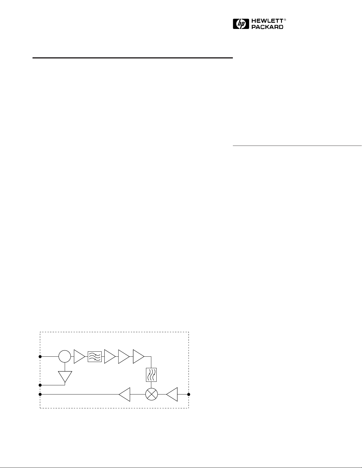
Block Diagram
Receiver Module
Tuning
Voltage
LO X3
MMICMMICBPF
AMPAMP
Description
This digital radio receiver module
provides the RF receive and down
conversion function for 23 GHz
digital radios. These modules offer
excellent phase noise performance and can be easily phase
locked to a frequency reference.
The receiver module provides an
output power of 3␣ dBm at the IF
frequency and is ideal for use in
radios using 2 and 4 level FSK
modulation. The excellent low
noise figure is achieved by using
the Hewlett-Packard PHEMT
MMIC technology coupled with an
image reject mixer. The receiver
module features an integrated
ultra low noise silicon bipolar
MMIC
X2A
VCO operating in the S/C band as
the local oscillator. A portion of
the oscillator output is coupled off
and is applied to a frequency
divider network. The low frequency output from the frequency
divider can then be easily used to
phase lock the source. The local
oscillator output is applied to a
frequency multiplier network to
produce the desired LO frequency
to the mixer.
Applications
This digital radio receiver module
provides the total RF receive and
down conversion function in
radios operating in the 21.2 to
23.6␣ GHz band.
Signal
Sample
Output
IF
Output
+4
5965-5087E
MSA-1100
MMIC
AMP
MIXER
BPF
MMIC
LNA
RF
Input
8-4
21.2 to
23.6 GHz
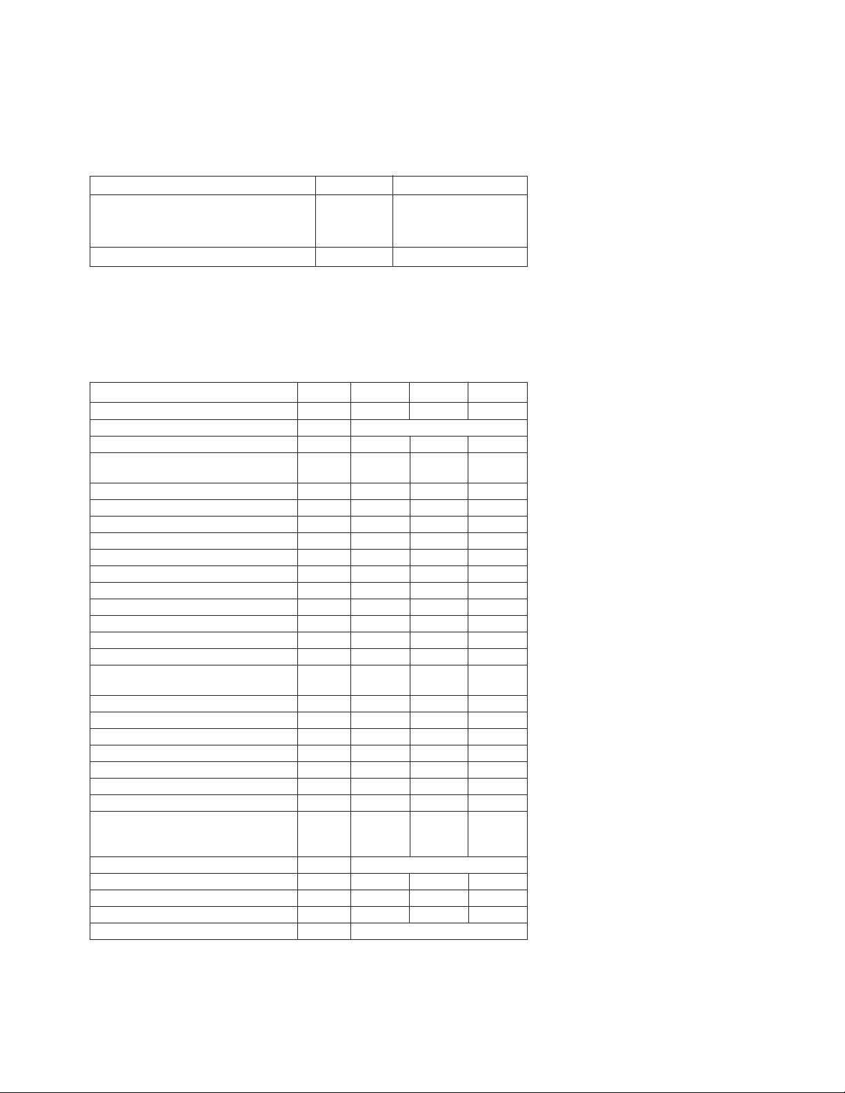
DRR1-23XX Absolute Maximum Ratings (T
= -30 to +70ºC)
A
Parameters Units Ratings
DC Circuit Power +8.5 Volts 10
+5.0 Volts +5.5
-5.0 Volts -5.5
Tuning Voltage Volts 14
Notes:
1. Operation in excess of any one of these parameters may result in permanent
damage.
2. A thermal interface medium must be used between the bottom of the
package and its mating surface to ensure optimum heat transfer.
DRR1-23XX Electrical Characteristics
Parameters Units Min. Typ. Max.
RF Tuning Range GHz 21.2 23.6
IF Frequency MHz 630 or 1260
IF Bandwidth MHz ± 20
LO Frequency GHz 20.57 22.97
or 19.94 o r 22.34
Gain dB 18 26
Gain Flatness over 300 MHz dB ±1
Noise Figure dB 4.5 5.5
Operating Temperature Range °C -30 70
Storage Temperature Range °C -45 85
Power Input at P-1dB dBm -22 -17
LO Leakage at I
LO Leakage at R
Return Loss RF Port dB 12
Return Loss IF Port dB 14
Image Rejection dB 12 15
Sample Out Frequency MHz 857 957
Sample Out Power dBm -10 0
Spurious Output
Phase Noise @ 100 KHz dBc/Hz -85 -82
Tuning Voltage V 1 12
Input Capacitance, Nom pf 1,000
LO Tuning Sensitivity MHz/V 300 500
LO Tuning Sensitivity Variation 1.5 : 1 2.0:1
DC Circuit Power: 8.5 Volts mA 300
5 Volts mA 400
-5 Volts mA 30
Case Dimensions inches 3.5 x 1.25 x 0.40
Max Power at Input/no damage dBm 10
Humidity Non Condensing % 85
Condensing % 95
Connectors WR 42 or SMA
Notes:
1. LO and Harmonic/sub-harmonic leakage at I with RF terminated into a 50␣ Ω load.
2. LO and Harmonic/sub-harmonic leakage at R up to 50 GHz.
3. Measured at IF port within the IF bandwidth with single tone RF input of <- 20 dBm.
[1]
[2]
[3]
dBm -15
dBm -15
or 831 or 931
dBc -60
8-5

DRR1-23XX Typical Performance
28
Spec Max
26
24
22
GAIN (dB)
T = +25°C
20
T = –30°C
T = +70°C
18
Spec Min
16
21 2322 24 21 2322 24
FREQUENCY (GHz)
Figure 1. Conversion Gain vs.
Frequency.
30
T = +25°C
T = –30°C
25
T = +70°C
20
15
Spec Min
IMAGE REJECTION (dB)
10
5
FREQUENCY (GHz)
Figure 2. Image Rejection vs.
Frequency.
6
Spec Max
5
4
NOISE FIGURE (dB)
3
T = +25°C
T = –30°C
T = +70°C
2
21 2322 24
FREQUENCY (GHz)
Figure 3. Noise Figure vs. Frequency.
-12
-14
-16
-18
(dBm)
IN
P
-20
-22
Spec Min
-24
21 2322 24
FREQUENCY (GHz)
Figure 4. Power In at P
Frequency.
T = +25°C
T = –30°C
T = +70°C
1dB
Out vs.
Powering Up Instructions
The -5 volts must be applied to the
receiver module before applying
the +5 volts. Likewise when
shutting down the receiver
module the +5␣ volts must be
removed before the -5 volts is
-40
-60
-80
dBc (Hz)
-100
-120
-140
1 10 100 1000
KHz Offset from Carrier
Figure 5. Phase Noise at 23 GHz vs.
KHz Offset from Carrier.
turned off. The +8.5␣ volts can be
turned on in any sequence. Failure
to follow this procedure could
cause permanent damage to the
module.
24
TUNING VOLTAGE
23
22
FREQUENCY (GHz)
21
14562 3 7 8 9 10 11 12
TUNING VOLTAGE (V)
MODULATION
SENSITIVITY
Figure 6. Tuning Voltage vs. Frequency
and Modulation Sensitivity.
Mounting Instructions
Case must be mounted firmly,
with screws, to an adequate
metallic structure that has sufficient thermal properties to
maintain the module case at a
temperature not to exceed 70° C.
400
350
300
250
MODULATION SENSITIVITY (MHz/V)
200
Product Options
Specify part number followed by option. For example:
DR R 1 – 23 X X
Model Number Prefix = Digital Radio
R = Receiver Module
Internal Use
8-6
1 = SMA Connector
2 = WR-42 Waveguide Connector
1 = 630 MHz IF Frequency
2 = 1260 MHz IF Frequency
23 = 21.2 to 23.6 GHz Frequency Band

Case Dimensions (specified in inches)
1.250
11x .200
GND
1F
+8.5V
H
DRRI-23XX
S/N XXXX
+8.5V
+5V
-5V
3.50
2.700
GND
F/4
+5V
VT
D/C XXXX
GND
.40 MAX
SEE DETAIL A
.445
.445
.170
.120
.820
1.10
.670
1.70
2.35
8x .100
2.430
11x .220
11x Ø .025
.500
.500
6x Ø
.125
.120
THRU
.420
.640
Ø .067 ±.001
.100
4X 4-40 UNC-2B
.120
.375
DETAIL A
8-7
 Loading...