

Page 1
SERVICE MANUAL
HP D8911A
Page 2

TABLE OF CONTENTS
PAGE
1. SPECIFICATIONS ..................................................................................................... 3-4
2. PRECAUTION AND NOTICES ................................................................................ 5
2-1 SAFETY PRECAUTIONS .............................................................................. 5
2-2 PRODUCT SAFETY NOTICE ....................................................................... 5
2-3 SERVICE NOTES ........................................................................................... 5
2-4 HIGH VOLTAGE WARNING ....................................................................... 6
3. OPERATING INSTRUCTIONS ................................................................................ 7
4. ADJUSTMENT .......................................................................................................... 8
4-1 ADJUSTMENT CONDITIONS AND PRECAUTIONS ............................... 8
4-2 MAIN ADJUSTMENTS ................................................................................. 8
4-3 ADJUSTMENT METHOD ............................................................................. 8-10
5. CIRCUIT DESCRIPTION .......................................................................................... 11
6. TROUBLE SHOOTING CHART .............................................................................. 15
6-1 NO RASTER, CRT RELATIVE CIRCUIT PROBLEMS .............................. 15
6-2 ABNORMAL DISPLAY ................................................................................. 17
6-3 NO BLANKING ........................................................................................... 18
6-4 HOR. /OSC /DEF /HV CIRCUIT FAULT ...................................................... 18
6-5 ABNORMAL HORIZONTAL DEFLECTION .............................................. 19
6-6 ABNORMAL VERTICAL SCANNING ........................................................ 20
6-7 SIDE-PIN CUSHION DISTORTION ............................................................. 20
6-8 POOR FOCUS ................................................................................................. 20
6-9 POWER SUPPLY TROUBLE SHOOTING CHART .................................... 21
7. MECHANICAL OF CABINET FRONT DIS-ASSEMBLY...................................... 22
8. PARTS LISTING ....................................................................................................... 23
9. BLOCK DIAGRAM (DEFLECTION) ....................................................................... 44
10. IC BLOCK DIAGRAMS............................................................................................ 45
11. PCB LAYOUT ............................................................................................................ 49
12. SCHEMATIC DIAGRAM ......................................................................................... 51
Page 3

1. SPECIFICATIONS FOR C993 SERIES COLOR MONITOR
1. CRT : 48.2CM(19") 90 Deflection, 29mm Neck, 0.26mm Dot Pitch, Non-Glare Screen
2. Viewable image Size: 45.7CM (18") diagonal
3. Display Color: Unlimited Colors
4. External Controls:
Power On/O ff, OSD key, Fu nction knob: Co ntrast, Bright ness, H-Size, H- Center, V-Siz e, V-Center, ZO OM,
Pincushion, Trapezoid, Pin-Balance, Parallelogram, Rotation, Moire Reduce, Recall, Degaussing, Color
Temperature.
5. Input Video Signal
Mode 1 Mode 2 Mode 3 Mode 4 Mode 5
RGB Analog RGB Analog RGB Analog RGB Analog RGB Analog
Horiz. Sync: TTL Level TTL Level TTL Level TTL Leve l TTL Level
Negative Negative Positive Positive Positive
Vert. Sync : TTL Level T TL Level TTL Level TTL Level TTL Level
Positive Negative Positive Positive Positive
Horizontal: 640 (H) 720 (H) 800 (H) 800 (H) 1024 (H)
Vertical : 480 (V) 400 (V) 600(V) 600 (V) 768 (V)
Fh (kHz) : 31.47 31.47 46.875 53.67 60.02
Fv (Hz) : 60 70 75 85 75
Mode 6 Mode 7 Mode 8 Mode 9
RGB Analog RGB Analog RGB Analog RGB Analog
Horiz. Sync: TTL Level TTL Level TTL Level TTL Level
Positive Positive Positive Positive
Vert. Sync : TTL Level TTL Leve l TTL Level TTL Level
Positive Positive Positive Positive
Horizontal: 1024 (H) 1280 (H) 1280 (H) 1600 (H)
Vertical : 768 (V) 1024 (V) 1024 (V) 1200 (V)
Fh (kHz) : 68.6 79.6 91.1 93.8
Fv (Hz) : 85 75 85 75
6. Display Size
Horizontal: 346 mm
Vertical: 260 mm
7. Scanning Frequencies
Horizontal:
Vertical:
8. Factory Preset Timings: 9
User Timings: 20
9. Misconvergence
Center: 0.3 mm Max.
Corner: 0.4 mm Max.
10. Video Dot Rate: 202 MHz
30KHz ~ 96KHz
50 Hz ~ 160 Hz
Page 4

11. Power Source:
Switching Mode Power Supply
AC 100 ~240V, 50/60Hz Universal Type
12. Operating Temperature: 0°C to 40°C Ambient
13. Humidity : 10% to 85% Relative, Non-Condensing
14
Weight: 20.0 Kgs(Net), 23.8Kgs(Gross)
•
15 Dimensions Monitor:
Carton:
Monitor:
16. External Connection :
15 Pin D-type Connector AC Power Cord
17. Regulations: T ÜV/ERGO, TÜV/GS, CE, NEMKO
574(W) × 537(H)
460(W)
466(H)
×
TCO’99
594(D) mm
×
470(D) mm
×
Page 5

2. PRECAUTIONS AND NOTICES
2-1 SAFETY PRECAUTIONS
1. Observe all caution and safety related notes located inside the d isplay cabinet.
2. Operation of the display with the cover removed, may cause a serious shock hazard from the display power
supply. Work on the display should not be attempted by anyone who is not thoroughly familiar with
precautions necessary when working on high voltage equipment.
3. Do not install, remove or handle the picture tube in any manner unless shatter-proof goggles are worn.
People who are not so equipped should be kept away while handling picture tube. Keep picture tube away
from the body while handling.
4. The picture tube is constructed to limit X-RAY radiation to 0.5 mR/HR. For continued protection, use the
designated replacement tube only, and adjust the voltages so that the designated maximum rating at the
anode will not be exceeded.
5. Before returning a serviced display to the customer, a thorough safety test must be performed to verify that
the display is safe to operate without danger or shock. Always perform an AC leakage current check on the
exposed metallic parts of the cabinet, such as scre w heads.
Test method for current leakage is described as follow.
(a) P lug the AC line cord directly into rated AC outlet (do not use a line isolation transformer during this
check).
(b) Use an AC voltmeter having 5000 ohms per volt or with more sensitivity in the following manner:
Connect a 1500 ohms 10 Watt resistor, paralleled by a 0.15UF, AC type capacitor between a known
good earth ground (water pipe, conduit, etc.) and the exposed metallic parts simultaneously. Measure
the AC voltage across the combination of 1500 ohms resistor and 0.15UF capacitor.
(c) Reverse the AC plug at the AC outlet and repeat AC voltage measurements for each exposed metallic
part.
(d) Voltage measured must not exceed 0.5 volts RMS. This corresponds to 0 .35 milliamp AC. Any value
exceeding this limit constitutes a potential shock hazard and must be corrected immediately.
2-2 PRODUCT SAFETY NOTICE
Many electrical and mechanical parts in this chassis have special safety visual inspections and the protection
afforded by them cannot necessarily be obtained by using replacement components rated for higher voltage,
wattage, etc. Before replacing any of these components read the parts list in this manual carefully. The use of
substitute replacement parts which do not have the same safety characteristics as specified in the parts list ma y
create shock, fire, X-RAY radiation or other hazards.
2-3 SERVICE NOTES
1. When replacing parts or circuit boards, clamp the lead wires around terminals before soldering.
2. When replacing a high wattage resistor (more than 1/2W of metal oxide film resistor) in circuit board, keep
the resistor about 10mm (1/2 in) away from circuit boa r d.
3. Keep wires away from high voltage or high temperature components.
4. Keep wires in their original position so as to re duce interference.
Page 6

Operation of monitor outside of cabinet or with back removed may cause a serious shock hazard. Work on this
model should only be performed by those who are thoroughly familiar with precautions necessary when working
on high vo l tage equi pment.
Exercise care when servicing this chassis with power applied. Many B plus and high voltage terminals are
exposed which, if carelessly contacted, can cause serious shock or result in damage to the chassis. Maintain
interconnecting ground lead connections between chassis and picture tube dag when operating chassis.
Certain HV failures can increase X-ray radiation. Monitor should not be operated with HV levels exceeding the
specified rating for the chassis type. The maximum operating HV specified for the chassis used in this monitor is
26KV ± 1KV
with a line voltage of 120/240 VAC. Higher voltage may also increase possibility of failure in HV supply.
It is important to maintain specified values of all components in the horizontal and high voltage circuits and
anywhere e lse in the monitor that coul d cause a rise in high volta ge or opera ting supply vo ltages. No cha nges
should be made to the original design of the monitor. Components shown in the shaded areas on the schematic
should be replaced with exact factory replacement parts. The use of unauthorized substitute parts may create a
shock, fire or other hazard.
To determine the presence of high voltage, use an accurate, high impedance, HV meter connected between
second anode lead and CRT dag grounding device. When servicing the High Voltage System, remove static
charge from it by connecting a 10K ohm resistor in series with an insulated wire (such as a test probe) between
picture tube dag and 2nd anode lead.(AC line cord disconnected from AC power outlet.)
The picture tube used in this monitor employs integral implosion protection. Replace with tube of the same type
number for continue safety. Do not lift picture tube by the neck. Handle the picture tube only after discharging
the high voltage completely.
Page 7
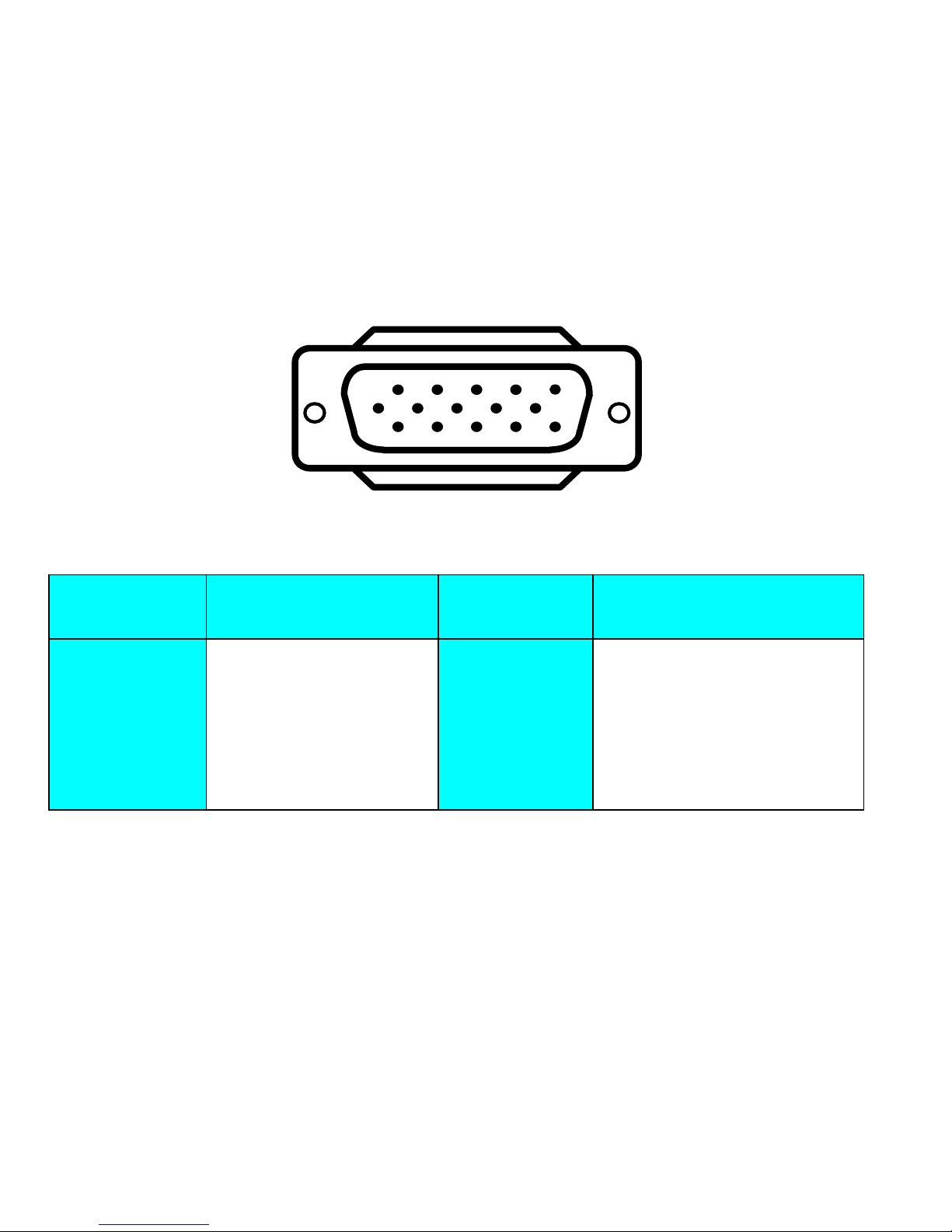
3. OPERATING INSTRUCTIONS
This procedure gives you instructions for installing and using the C993 color display.
1. Position the display on the desired operation and plug the power cord into a convenient AC outlet. T hreewire power cord must be shielded and is provided as a safety precaution as it connects the chassis and
cabinet to the electrical conduit ground. I f the AC outlet in your location d oes not have provisions for the
grounded type plug, the installer should attach the proper adapter to ensure a safe ground potential.
2. Connect the 15-pin color display shielded signal cable to your signal system device and lock both screws
on the connector to ensure firm grounding. The connector information is as follow:
15 - Pin Color Displa y Signal Cable
PIN NO.
DESCRIPTION
PIN NO.
DESCRIPTION
1. RED 9. NC
2. GREEN 10. GND
3. BLUE 11. SYNC. GND
4. GND 12. SDA
5. GND 13. HORIZ. SYNC
6. GND-R 14.
VERT. SYNC (VCLK)
7. GND-G 15. SCL
8. GND-B
3. Apply power to the display by turning the power switch to the "ON" position and allow about thirty
seconds for display tube warm-up. The Power-On indicator lights when the display is on.
4. With proper signals feed to the display, a pattern or data should appear on the screen, adjust the brightness
and contrast to the most pleasing display.
5. T his monitor has po wer saving function following the VES A DPMS. Be sure to connect the si gnal cable to
the PC.
6. If your C993 Series color display requires service, it must be returned with the power cord.
1
6
11 15
5
10
Page 8

4. ADJUSTMENT
4-1 ADJUSTMENT CONDITIONS AND PRECAUTIONS
1. Approximately 30 minutes should be allowed for warm up before proceeding.
2. Adjustments should be undertaken only on those necessary elements since most of them have been carefully
preset at the factory.
4-2 MAIN ADJUSTMENTS
NO. FUNCTION LOCATION DESIGNATION
1. 14.5V ADJ PCB - MAIN VR901
2. B + ADJ PCB - MAIN VR902
3. SCREEN ADJ FLY BACK TRANS T402
4. FOCUS ADJ FLY BACK TRANS T402
5. ABL ADJ PCB - MAIN VR701
6. SUB-BRIGHTNESS ADJ PCB - MAIN VR702
-MENU
2
PCB - MAIN SW103
-UP
PCB - MAIN SW105
7. FUNCTION ADJ -DOWN
PCB - MAIN SW104
-EXIT
1
PCB - MAIN SW102
4-3 ADJUSTMENT METHOD
1. 14.5V, B + & HV voltage adjustment:
A. Chrome-2000 Signal generator or PC equivalent set mode 1, VGA 640X480 pattern 1.0 .
B. Connect a DC Volt meter between TP901 or D922 cathode and ground, then adjust VR901 to be 14.5VDC.
C. Connect a DC Volt meter between TP902 or D925 cathode and ground, then adjust VR902 to be 60.5 VDC.
D. Connect a DC Volt meter between TP701(G1) and ground, Brightness set to max. T hen adjust VR702 to
be -50 VDC.
2. Factory preset Timings Adjustment:
A. Press MENU Key to show OSD window press Up or Down Key to switch the functional controls.
B. Press the Up Key to select the "ZOOM" function, then press the MENU Key. While do not release the
MENU Key until the OSD window changed to the Factory preset window.
C. The Factory preset window contains the following functional controls. Select one of the control. Then press
the Up/Down Key to adjust it's value for the optimum picture.
Page 9
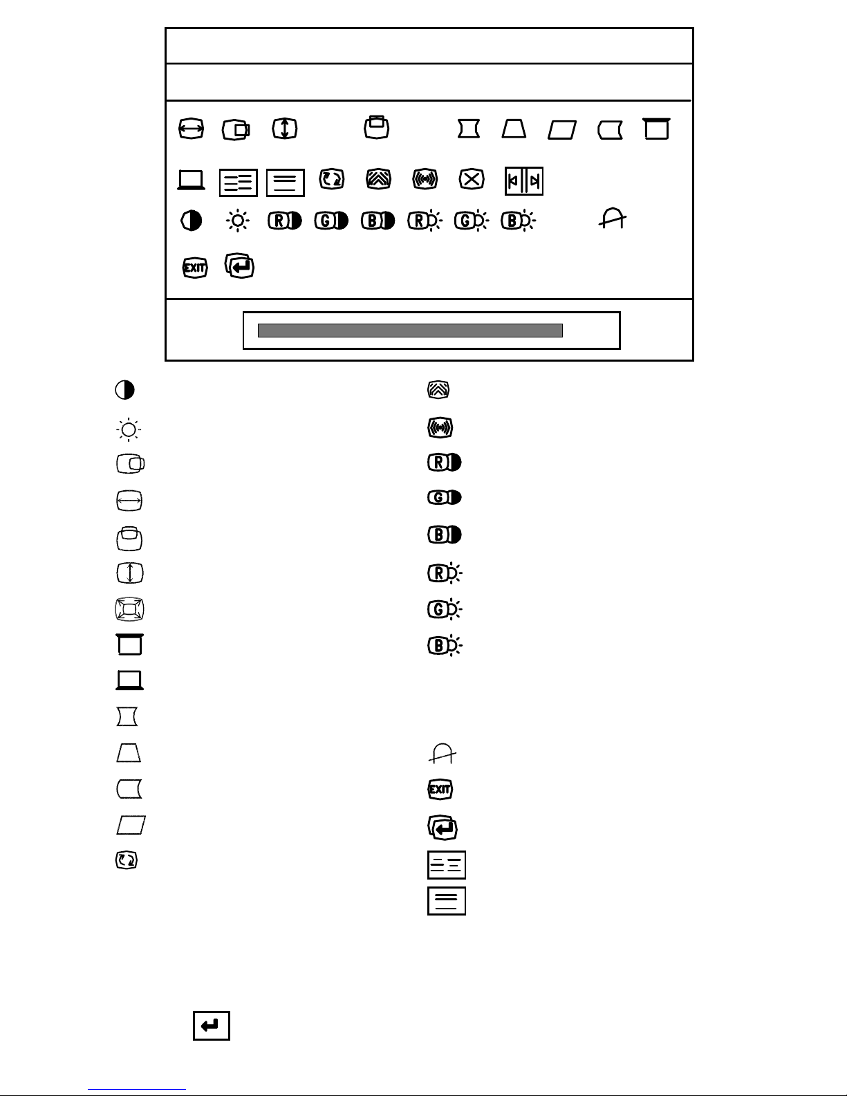
FACTORY PRESET
H: 36.51kHz
V: 51.34Hz
VcVs
9300
6500
Tm
080
CONTRAST
BRIGHTNESS
H-CENTER
H-MOIRE REDUCE
V-MOIRE REDUCE
R-GAIN
Vs
Vc
H-SIZE
V-CENTER
V-SIZE
ZOOM
TOP COMER
BOTTOM COMER
PINCUSHION
TRAPEZOID
PIN-BALANCE
PARALLELOGRAM
ROTATION
SUB-V-SIZE
SUB V-CENTER
9300
6500
G-GAIN
B-GAIN
R-BIAS
G-BIAS
R-BIAS
COLOR TEMPERATURE
COLOR TEMPERATURE
DEGAUSS
OSD EXIT
RETURN
Vs LINEAR
Vc LINEAR
MENU Key to Quit the OSD window. Mean while the new setting data will be saved in t he memory.
E. To switches the input signal to the other Timing Mode. Please follow step C ~ D to get the optimum picture.
F. Select the "
returned to the original OSD window.(user's operating condition)
" RETURN function and press t he MENU Key, then the Factor P reset windo w will be
Page 10
G. The setting data of the CONTRAST, BRIGHTNESS, PIN-BALANCE, PARALLELOGRAM,
ROTATION, COLOR TEMPERATURE are common mode saved in the memory. Don't needed adjust it
individual at every timing Mode and save in the memory.
H
Model select: for factory only, service engineer can't changed.
3. White Balance, Luminance adjustment:
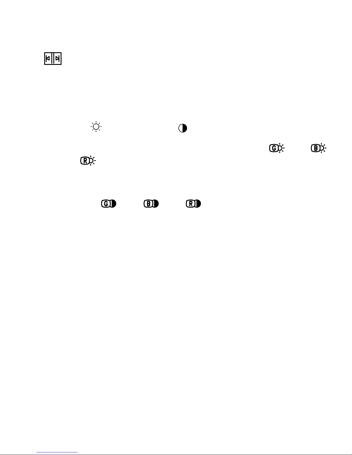
A. B ias (Low Luminance) adjustment:
(a) Set mode 2 640 X 480 Fh: 31KHz full white pattern.
(b) To make the adjustment condition is under the Factory preset window.
Same as step 2-C.
(c) Warm up more than 20 minutes.
(d) Brightness
set to maximum. Co ntrast set to min. full white pattern, the n adjust FBT screen
VR to make Y= 1.0FL ± 0.2FL
(e) Brightness set to raster just cutoff, adjust con t rast to be 4FL, the n adjust G-Bias
R-Bias
, to make the setting value is( 20), then adjust the R.G.B Bias individual to the colo r
, B-Bias ,
temperature x= 281 ± 10, y= 311 ± 10.
B. Gain (High light) adjustment:
(a) Set mode 2 640 X 480 Fh: 31.5KHz full white pattern.
(b) Brightness set to raster just cutoff and set the contrast to max.
(c) Adjust G-Gain
10.
±
, B-Gain , R-Gain , to make color temperature x=283 ± 10, y=293
C. Recheck item A&B to make sure both of them in spec. Finally select OSD function to the 9300°K function,
then press the MENU Key. To make the setting data saved in the memory.
D. The adjustment of 6500°K white Balance, May follow step A ~ C , with the x=313 ± 10, y=329 ± 10.
E. Full white luminance:
(a) Set mode 2 640 X 480 Fh: 31.5KHz full white pattern.
(b) Image Size : H:346±4mm V:260±4mm.
(c) Brightness set to raster just cut off and set the contrast to max.
(d) Adjust VR701 to the luminance at 30 FL ± 2FL.
4. Focus Adjustment:
A. Set mode 2 640 X 480 Fh: 31.5KHz with character full page.
B. Adjust brig ht nes s to center an d contrast to max.
C. Then adjust focus VR1 to a fine vertical line.
D. Adjust focus VR2 to a fine horizontal line.
E. Repeat step C & D..
5. Purity Adjustment
A. Be sure that the display is no t being exposed to any external magnetic fields.
B. Ensure that the spacing between the Purity, Convergence, Magnet, (PCM), assembly and the CRT stem is
29mm .(See below diagram)
C. Pr oduce a complete, red pattern on the displa y. Adjust the purity magnet rings o n the PCM assembly to
obtain a complete field of the color red. This is done by moving the two tabs in such a manner that they
advance in an opposite direction but at the same time to obtain the same angle between the two tabs, which
should be approximately 180'.
D. Check the complete blue and complete green patterns to observe their respective color purity. Make minor
adjustments if needed.
Page 11

RELATIVE PLACEMENT OF TYPICAL COMPONENTS
Purity Magnets
6-pole Convergence Magnets
4-pole Convergence Magnets
Deflection Yoke
6. Convergence adjustment
A. Produce a magenta crosshatch on the display.
B. Adjust the focus for the best overall focus on the display.
Also adjust the brigh tness to the desired condition.
C. Vertical red and blue lines are converged by varying the angle between the two tabs of the 4 pole magnets
on the PCM assembly. (See above diagrams)
D. Horizontal red and blue lines are converged by varying the two tabs together, keeping the angle between
them constant.
E. Produce a white crosshatch pattern on the display.
F. Vertical gree n and magenta lines are converged by varying the angle between the two tabs of the 6-pole
magnets.
G. Horizontal green and magenta lines are converged by varying the two tabs together, keeping the angle
between them constant.
5. CIRCUIT DESCRIPTION
5-1 MICRO CONTROLLER CIRCUIT
MICRO Controller
The IC101 contains a 6502 8-bit CPU core, 256 bytes of RAM, 16K bytes of ROM,14 channel 8 bit PWM D/A
converters, 2 channel A/D converters for key detection, one 8 bit pre-loadable base timer, internal H-sync and
V-sync signals processor providing mode detection, watch- dog timer preventing system from abnormal operation,
and an I2C bus interface.
H/V sync signals proce ssor
The functions of the sync processor include polarity detection, H-SYNC & V-SYNC signals counting,
Programmable SYNC signals output, free running signal generator. Pin39/Pin40 are for the H-SYNC and
V-SYNC input, Pin32/Pin33 will output the same signal as input sync signal without delay, and the polarity are
setting in the positive. Whe n no signal input, the Pin32 wil l output a 61HZ V- SYNC free run si gnal. The Pin33
will output a 62.5KHz H-SYNC free run signal. for the monitor testing use.
Page 12

On Screen Display Controller
The IC103 is designed for display the built-in characters or fonts onto monitor screen. The display operation is by
transforming data and control information from micro controller to RAM through a serial data interface.
Pin2 is used to control the internal oscillator frequency by DC voltage input from external low pass filter (R125,
C114, R161) and filter (R126, C115) is used to regulate the appropriate bias current for internal oscillator the
resonate at specific dot frequency.
Pin5 is input the horizontal fly back pulse, for PLL generator tracking.
Pin6 is left floating, I2C bus is enabled. Otherwise the SPI bus is enabled.
Pin7 the external data transfer through this pin to internal display registers and control registers
Pin8 the clock-input pin is used to synchronize the data transfer.
Pin10 is input the vertical flyback pulse for synchronizing the vertical position.
Pin12 is output a blanking signal to cut off external R.G.B signals of VGA while this chip is displaying characters
or windows.
Pin13, Pin14, Pin15 is used to output the OSD (B.G.R) video signal.
5-2 DEFLECTION CIRCUIT
The deflection circuit is achieved by a high performance and efficient solution IC 401 (TDA4856) for this monitor.
The concept is fully DC controllable and can be used in applications with a micro-controller solutions.
The TDA 4856 provides sync. Processing with full auto sync. capability, a flexible SMPS block and an
extensive set of geometry con trol facilities. Further t he IC generates the dr ive wavefor ms for DC coupled vertical
boosters to the TDA 4866 [ref Page-28].
Horizontal Oscillator
The oscillator is of the relaxation type and requires a capacitor of 10nF C403 at pin 29. The maximum oscillator
frequency is determined by a resistor R403 form pin 28 to ground. A resistor R402 from pin27 to pin28 defines the
frequency range.
PLL 1 Phase Detector
The phase detector is a standard one using switched current sources. It compares the middle of H-sync. with a
fixed point on the oscillator saw-tooth voltage. The PLL loop filter c401, R401, C402 is connected to Pin26.
PLL2 Phase Detector
This phase detector is similar to the PLL1 detector and compares the line flyback pulse at pin 1 with the oscillator
saw-tooth voltage. The PLL2 detector thus compensates for the delay in the external H-deflection circuit by
adjusting the phase of the HDRV output pulses. The phase between H-flyback and H-sync can be controlled at
pin30.
X-ray Protection
The X-ray protection input pin2 provides a voltage detector with a precise threshold. If the voltage exceeds this
threshold for a certain time, an internal latch switches the whole IC into pro tectio n mode. In this mode several p ins
are forced into defined states:
Pin7 (HDRV) is floating
Pin6 (B DRV) is floa t ing
Pin12, 13 ( VOUT 1, 2) are floating
Pin16 (CLBL) provides a continuous blanking signal.
Vertical Oscillator
The vertical free –running frequency is determined by the resistor R608 at pin23 and capacitor C604 at pin24.
Usually t he free-running frequency should be lower than the minimum trigger freque ncy.
Page 13

5-3 TRANSISTOR & DIODE CIRCUI T
LOCATION
FUNCTION AL DESCRIPTION
D101 For C102 Discharge
Q101 For LED Indicator Control
D418 Protection Diode for Snubber Clip Diode ZD401
D431 Protection Diode for B+ Control
D405, D424 Speed up for Q403
D406, D407 Supply a bias for D408
D408 Damping Diode and Modulation Diode
Q416 B+ MUTE
D414~ D417,D419 Buffer Diode for IC403
D421 ~ D423 Detected for Q406
Q401 B+ Mute Control
Q402 Horizontal Driver
Q403 Horizontal Out Put
Q404, Q406 A differential Amp for Drive Q405
Q405 DarlingtonTransistor for H-Size Control
Q407 Horizontal Linearity Correction Control
Q410, Q412, Q417 Horizontal S-Correction Control
Q418, Q420 Horizontal S-Correction Control
ZD601,ZD602 VF Voltage Divider
D707 Mixing Diode
D703 Buffer Diode
D704 Rectifier for 250V Supply
D705 Protection Diode for Q708
Page 14

LOCATION
FUNCTION AL DESCRIPTION
D706,D708 Rectifier for -200V Supply
Q707 Picture Mute Control AMP
Q703, Q706 Brightness Control CKT
Q708 Vertical Dynamic Focus Control AMP
D901 ~ D904 Bridge Rectifier for AC Source
D909 Rectifier for Start Power Supply
D910 Clip Diode for Snubber CKT
D911 IC901 VCC Supply
D913 Speed UP for Q901
D914 Synchronous Trigger for Power Supply
D918 ~ D919 Rectifier for Output Voltage Supply
D921 ~ D923 Rectifier for Output Voltage Supply
D924 Clip Diode for Trigger CKT
D925 Rectifier for B+ Supply
D926, D927 Raster Position Control
D939 Clip Diode for Snuffer Pulse
ZD901 Protection Diode
ZD902 Protection Diode
ZD903 Protection Diode
Q901 MOS FET for Switching Power Control
Q904, Q906 Start up CKT for IC901
Q908, Q916 To Turn 6.3V Supply Off when the Off Mode is Required
Q909, Q910 To Turn 14.5V Supply Off when the Off or Suspend Mode is Required
Q911 MOS FET for B+ Control
Q912, Q915 Push Pull Driver for Q911
Q914 Pre-Amplifier for Q912, Q915
D817 ~ D819 DC Restoration for CRT Bias Adjustment
D814 ~ D816 Protection Diode for Q808, Q809, Q810, Q811, Q812, Q813
Q801 A.B.L Control
Q817 ~ Q819 DC Restoration for CRT Bias Adjustment
Page 15
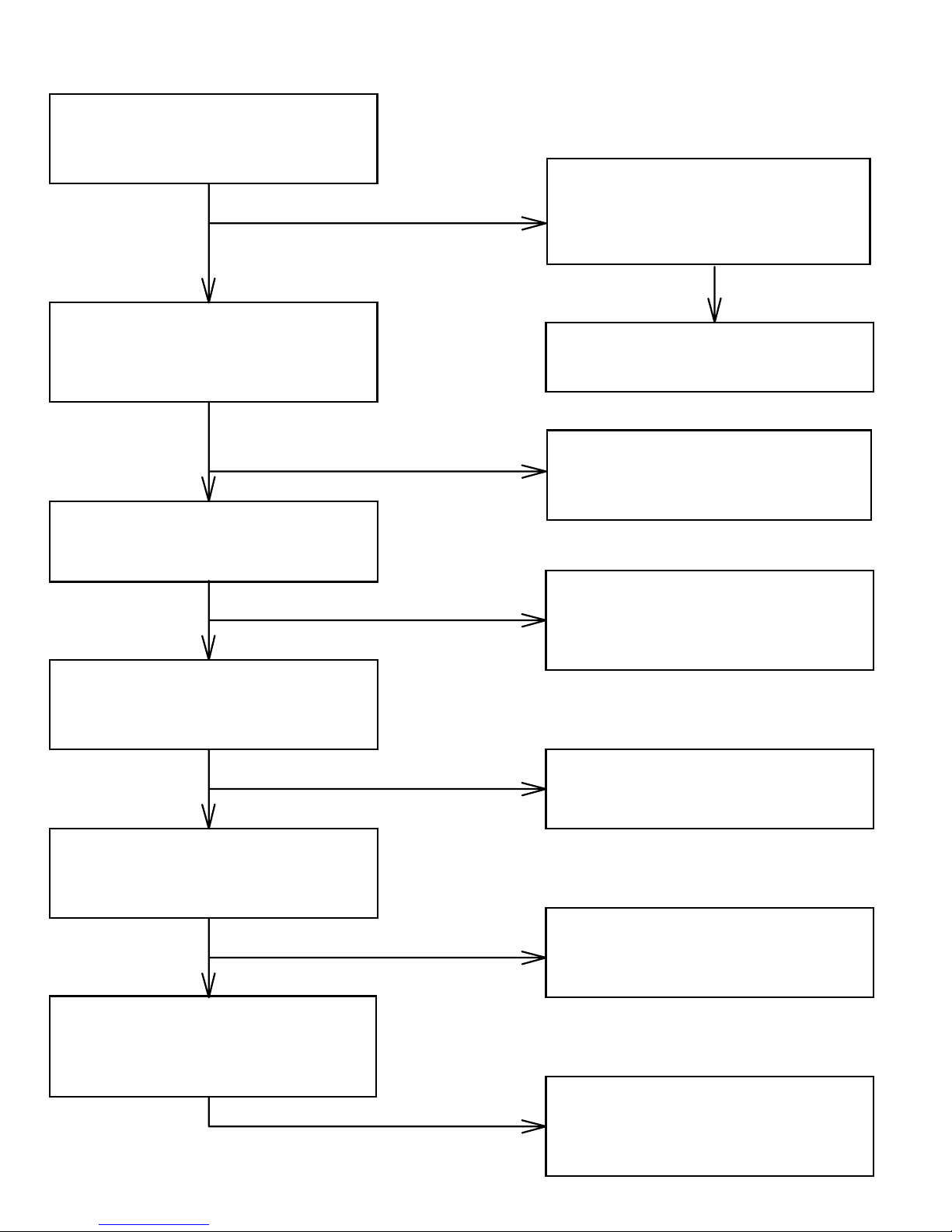
6.TROUBLE SHOOTING CHART
6-1 NO RASTER, CRT RELATIVE CIRCUIT PROBLEMS
CHECK MAIN PCB POWER SUPPLY
60.5V, 14.5V, 80V
NG
OK
CHECK THE HIGE VOLTAGE
OF CRT ABOUT 25.5 ~ 26.5KV
NG
OK
CHECK THE VOLTAGE OF CRT
HEATER ABOUT 6.3V
NG
OK
CHECK POWER SAVING CIRCUIT,
H-SYNC, V-SYNC SIGNAL
OK
REFER ITEM S.M.P.S.
CHECK FAILSAFE CKT IC401
PIN 2 RELATIVE CKT.
CHECK CRT'S HEATER RELATIVE
CIRCUIT
CHECK SCREEN VOLTAGE ABOUT
400V TO 700V
LESS THAN 300V
OK
BRIGHTNESS SET TO MAX.
THEN CHECK CRT G1 VOLTAGE
NG
OK
CHECK VOLTAGE OF THE CRT
CATHODE ABOUT 60V TO 70V
NG
CHECK FBT
CHECK BRIGHTNESS CIRCUIT
Q703, Q706, Q707 RELATIVE CKT.
REFER ITEM 8-2
"ABNORMAL DISPLAY"
Page 16
2.ABNORMAL VIDEO LEVEL ON SCREEN
CHECK THE VOLTAGE OF IC801
PIN 6, 9, 22 ABOUT 12V
NG
OK
CHECK THE SIGNAL INPUT OF R.G.B.
ABOUT 0.7Vpp
OK
CHECK IC801 PIN 15 CLAMP PULSE
PIN 16 BLANK PULSE
NG
OK
CHECK THE VIDEO OUTPUT OF IC801
PIN 18, 20, 23 ABOUT 4Vpp,
CONTRAST SET MAX.
NG
OK
CHECK 12V RELATIVE
CIRCUIT
CHECK SIGNAL CABLE OR
INTERFACE CARD.
CHECK THE IC105 RELATIVE CIRCUIT
OR IC401 PIN 16 OUTPUT
CHECK IC801 PIN 13 ABOUT 4V
PIN 26, 27, 28 ABOUT 4V OR
CHECK Q801 AND RELATIVE CKT
R.G.B. APPROACH STANDARD
3. ABNORMAL DDC (PLUG & PLAY)
CHECK IC101 PIN 5 VOLTAGE ABOUT 5V
NG
OK
CHECK SIGNAL CABLE
OR H802 PIN 3, 4 DATA OUTPUT
CHECK Q102 GOOD OR FAIL
Page 17
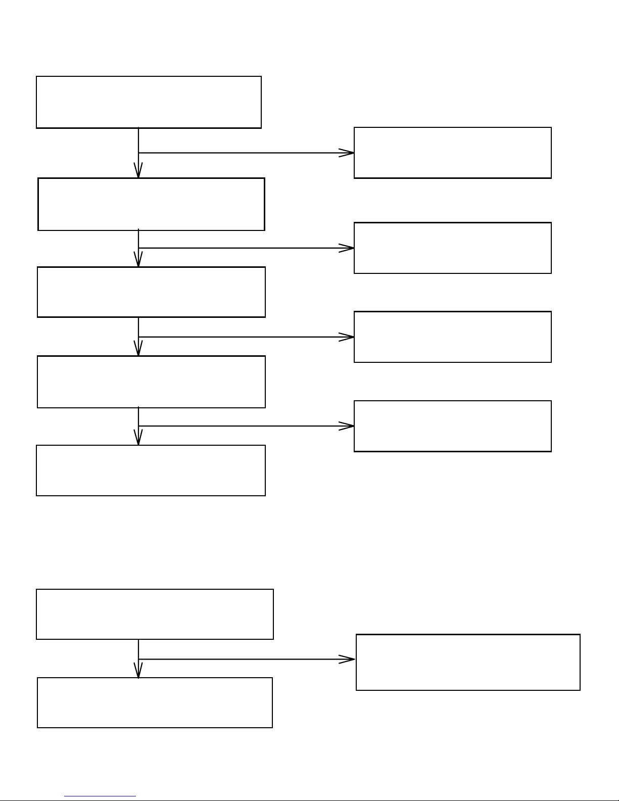
1.NO SIGNAL ON SCREEN
CHECK VIDEO IC801 VCC ABOUT 12V
6-2 ABNORMAL DISPLAY
NG
OK
CHECK THE OUTPUT VOLTAGE
OF IC801 PIN 18, 20, 23 ABOUT 3Vpp
NG
OK
CHECK THE B+ VOLTAGE OF
VIDEO PCB ABOUT 80V
NG
OK
CHECK THE VOLTAGE OF CRT
CATHODE ABOUT 40Vpp
CHECK THE 12V PIN
OF P802 CONNECTOR
CHECK THE RELATIVE CIRCUIT
OF IC801
CHECK THE 80V RELATIVE CIRCUIT
OF SMPS ON MAIN PCB
NG
OK
CHECK THE VOLTAGE OF FBT SCREEN
ABOUT 400V TO 700V
LESS THAN 400V
EXCEED 700V
CHECKTHE VQ802 ~ Q807
RELATIVE CIRCUIT
CHECK FBT RELATIVE
CIRCUIT
CHECK FBT & CRT RELATIVE CIRCUIT
OR REFER ITEM 7-1
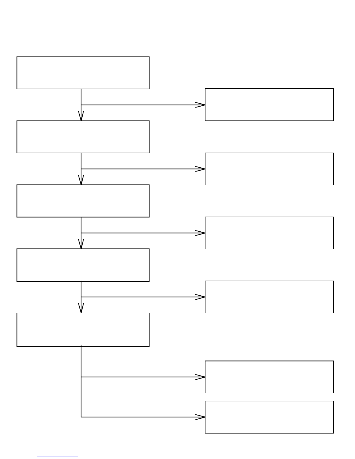
Page 18

CHECK THE RELATIVE
CIRCUIT OF BLANKING
6-3 NO BLANKING
NG
OK
CHECK IC801 PIN 16 ON VIDEO PCB,
CHECK G1 RELATIVE CIRCUIT
Q705, R718, C707 ON MAIN PCB
CHECK THE RELATIVE CIRCUIT
OF C433, D410, R635, R636, IC105
ON MAIN PCB
6-4 HOR./OSC/DEF/HV CIRCUIT FAULT
1. NO RASTER (DISCONNECT WITH SIGNAL CABLE)
CHECK IC401 PIN 10 ABOUT 11.5 VDC
NG
OK
CHECK IC401 PIN 8 WAVE FORM
ABOUT 10Vpp
NG
OK
CHECK THE COLLECTOR VOLTAGE
OF Q402 ABOUT 40Vpp
NG
OK
CHECK THE COLLECTOR VOLTAGE
OF Q403 ABOUT 1100Vpp AT FH:31KHz
CHECK IC401 PIN 10 RELATIVE CIRCUIT
CHECK IC401 PIN 26 ~ 31
RELATIVE CIRCUIT
CHECK Q402, T401
RELATIVE CIRCUIT
NG
CHECK T401, T402, Q402, Q403,
D408, C418, C419, H-DY
Page 19

6-5 ABN ORMAL HORIZONTAL DEF LECTION
1. ABNORMAL HORIZONTAL WIDTH OF VIDEO
READJUST H-WIDTH FUNCTION
NG
OK
CHECK FBT B+ VOLTAGE
ABOUT 60.5V AT FH=31KHz
CHECK THE HV OF
CRT ABOUT 26KV
2. ABNORMAL HORIZONTAL RASTER CENTER
CHECK THE RELATIVE CIRCUIT
OF Q404, Q405, & Q406
CHECK THE RELATIVE
CIRCUIT OF SMPS.
Q911, Q912, Q914, Q915 &
IC401 PIN 4, 5, 6, VR 902
CHECK T903, D926, D927, R964, R968
P403 AND JUMPER
3. ABNORMAL HORIZONTAL VIDEO CENTER
CHECK IC101 PIN 9, 10, IC401 PIN 18, 19
4. ABNORMAL HORIZONTAL LINEARITY
CHECK L401, Q407, R447, C448
AND IC101 PIN 20, 21, 22, 23
CS SWITCHER IC403, Q410, Q411, Q420
Page 20

6-6 ABNORMAL VERTICAL SCANNING
1. ABNORMAL VERTICAL SIZE
READJUST V-SIZE FUNCTION VALUE
CHECK THE IC601 PIN 7 ABOUT 40V
NG
OK
CHECK VERT. OSC CIRCUIT
NG
OK
CHECK IC601 PIN 6 OUTPUT ABOUT
38Vpp
2. VERTICAL CENTER
CHECK ZD601, ZD602 R626 & SMPS
RELATIVE CIRCUIT
CHECK IC401 PIN 22, 23, 24
NG
CHECK IC401 PIN 12, 13
RELATIVE CIRCUIT
READJUST V-CENTER
NG
6-7 SIDE-PIN CUSHION DISTORTION
READJUST SIDEPIN
NG
CHECK IC101 PIN 9, 10
IC401 PIN 18, 19
CHECK IC401, Q404, Q405, Q406
RELATIVE CKT.
Page 21

6-8 POOR FOCUS
READJUST FOCUS CONTROL
NG CHECK FOCUS CONTROL UNIT, FOCUS
LEAD WIRE, CRT SOCKET & CRT
6-9 NO SOUND (FOR AUDIO MODEL ONLY)
OK
OK
OK
OK
NG
ENSURE THE SOUND SOURCE
IS POWER ON
ENSURE THE SOURCE CABLE
CONNECTION
CHECK POWER
CHECK IC501
IC501 FAILURE
SPEAKER FAILURE
OK
SUPPLY CIRCUIT
ADJUST VOLUME CONTROL
NG
CHECK IC501
PIN 14 ABOUT 14V
Page 22

6-10 POWER SUPPLY TROUBLE SHOOTING CHART
BEFORE CHECK SW.REG. PLEASE REFER TO THE POWER SUPPLY BLOCK DIAGRAM
POWER SUPPLY OUTPUT: (A) VARIABLE OUTPUT : 60.5V - 145V
(DEPENDING EPENDING UPON H.SYNC FREQUENCY)
(B) CONSTANT OUTPUT : 6.3V, 14.5V, 55V, 80V
BEAD SET
CHECK AC LINE
VOLT 120V OR 220V
NG
OK
CHECK LINE RECTIFIED
& SMOOTHED VOLT
NG
OK
CHECK START C.K.T
D909, Q904, R922, R925
CHECK F901, SW901
CHECK BRIDGE
RECTIFIED CIRCUIT
ABNORMAL VARIABLE OUTPUT
MAKE SURE THAT
THE VARIABLE
OUTPUT IS NOT SHORTED
NO
YES
CHECK THE C934
VOLTAGE 55V
NG
OK
CHECK IC401
PIN 4, 5, 6, B+ DRIVER
CHECK D919
NG
OK
CHECK T901 O/P
NG
OK
CHECK IC901
NG
OK
CHECK Q901
CHECK POWER SAVING
C.K.T(OFF-MODE)
CHECK 80V, 55V, 14.5V
6.3V CIRCUIT
IC901 FAILURE
CHECK Q911
NG
Q911 FAILURE
OK
CHECK Q912, Q914, Q915
NG
CHECK Q901
OK
Page 23

7. MECHANICAL OF CABINET FRONT DIS-ASSEMBLY
Page 24

PARTS LIST OF CABINET
LOCATION C993 SPECIFICATION
(LOW RADIATION 220V)
C995TSE CHAS ASS'Y
1A 503- 5 - 47 SCREW
5A 38- 8 RUBBER WASHER
9A 84- 22 LUG
11A 112- 500 WIRE MOUNT
11A 115- 1 F.B.T CLIP
12A 381- 500 RUBBER FOOT
19A 403- 7 STEEL
19A 506- 2 STEEL WIRE SPRING
33A 3663- 1 SUPPORT
33A 3726- 1 POWER CAP
33A 3727- 1 POWER ROD
33A 3790- 1 POWER LED LENS
33A 3793- 311 - AT POWER BUTTON
33A 3794- 311 - AT KEY PAD
34A 604- 311 - LT BASE
34A 639- 311 - AL SWIVEL
34A 668- 311 - 1AT BACK CABINET
34A 682- 311 - 2AT FRONT PANEL
40A 152- 502 LABEL
40A 152- 509 RECYCLE LABEL
40A 152- 512 RECYCLE LABEL
40A 153- 74 - 2 LABEL
40A 154- 14 - 1 CABINET LABEL
40A 154- 501 - 1 HI-POT GND LABEL
40A 581- 26 - 668 SLZ LABEL
40A 581- 26 - 704 LABEL
40A 2029- 622 - 1A ID LABEL
!
!
!
40A 68- 508 - A CARD
41A 68- 615 - 4A TCO99 CARD
41A 68- 622 - 1B WARRANTY CARD
41A 550- 622 - 1B OWNER'S MANUAL
44A 3200- 1 EPS CUSHION(L)
44A 3200- 2 EPS CUSHION(R)
44A 3200- 622 - 1A CARTON
45A 76- 28 - RN PE BAG
45A 76- 34 - RN PE BAG
45A 76- 502 - RN PE BAG
45A 77- 3 TRANSPARENT SHEET
45A 77- 500 BARCODE RIBBON
45A 77- 501 BARCODE RIBBON
85A 532- 2 CRPC SHIELD
85A 543- 507 CRPC SHIELD
85A 578- 1 - A EMI SHIELD
89A 404A- 15N - IS POWER CORD UL/CSA
95A 91- 205 - 598 WIRE
95A 207- 10 WIRE
B1A 1035- 10 - 128 SCREW
B1A 1040- 8 - 128 SCREW
M1A 1130- 8 - 128 SCREW
Q1A 340- 16 - 128 SCREW
Q1A 1030- 10 - 128 SCREW
750A 1697- 75 - A DEG. COIL UL/CSA
750A 5455- 1AV M46QCG903*21(A) 19” LG
Page 25

LOCATION C993 SPECIFICATION
1A 421- 4 - 128 SCREW
2A 202- 4 STAINLESS STEEL CLIP
3A 1- 4 - 106 LOCK WASHER
6A 31- 4 BRASS
9A 203- 8 BRASS PIN
11A 86- 2 NYLON
11A 127- 1 PC SUPPORT
15A 5640- 1 - A AL GND LUG
15A 5659- 500 - 2 REAR BRACKET
40A 581- 26 - 702 FAIL-SAFE LABEL
40A 581- 624 - 2A CHASSIS LABEL
50A 500- 1 CABLE TIE
62A 10- 16 - W SPARK GAP 1KV
89A 174A- 5EC - GL SIGNAL CABLE
95A 201- 69
95A 201- 69
95A 201- 69
B1A 1040- 8
B1A 1040- 10
B1A 1140- 8
M1A 1140- 6
705A 995T- C56
705A 995T- C56
705A 995T- C57
705A 995T- C57
705A 995T- C57
705A 995T- C57
705A 995T- C87
705A 995T- C93
715A 787- B
750A 5455- 995
750A 5455- 995
750A 5455- 995
<SW102> 77A 602- 1
<SW103> 77A 602- 1
<SW104> 77A 602- 1
<SW105> 77A 602- 1
AS2 95A 205T- 30 - 072
C411 67A 309- 102 - 3
C414 67A 305- 470 - 9L
C415 65A 517K- 103 - 1A 10000PF Z5F 500V
C418 63A 210J- 432 - 8MK
C419 63A 210J- 432 - 5FC
C425 63A 210J- 224 - 3CJ
C426 63A 210J- 684 - 2CC
C428 63A 210J- 122 - 7FM
C429 63A 210J- 394 - 2CC
C431 64A 100J- 225 - 59
C438 63A 210J- 224 - 2CC
C439 63A 210J- 394 - 2CC
C458 63A 210J- 124 - 2BF
C610 67A 305- 101 - 9T
C615 67A 305- 102 - 3
C703 67A 305- 109 - 15
C713 67A 305- 100 - 12
!
C900 65A 305M- 472 - 2B2 4700P F +-20% 400VAC
C903 65A 305M- 332 - 2B2 3300P F +-20% 400VAC/250V
C904 65A 305M- 332 - 2B2 3300P F +-20% 400VAC/250V
C907 67A 30- 221 - 14D 220Uf +-20% 400V
PARTS LIST OF CHAS
AI995TSE
CR995TSE CRT BOARD ASS'Y
032
-
042
-
052
-
128
-
128
-
128
-
128
-
-
-
-
-
-
-
-
-
-
-
-
-
-
-
-
01
02
02
03
04
01E
01
01
SDT
SET
SIT
HJ
HJ
HJ
HJ
MAIN BOARD ASS'Y
WIRE
WIRE
WIRE
SCREW
SCREW
SCREW
SCREW
IC601 ASS'Y
IC904 ASS'Y
Q901 ASS'Y
Q425 ASS’Y
Q420 ASS’Y
Q403/Q405/Q911/D408 ASS’Y
CN901 ASS’Y
D921 ASS’Y
GROUND PANEL
19” LG TCO99 CRT ASS’Y
19” LG TCO CRT ASS’Y
19” LG MPRII CRT ASS’Y
TACT SW TSVB-3B
TACT SW TSVB-3B
TACT SW TSVB-3B
TACT SW TSVB-3B
WIRE ASS’Y
1000uF +-20% 16V
47uF +-20% 10 0V
4300PF 2KV 5A
4300PF 1000V +-5%
0.22uF 400V 15A
0.68uF 250V +-5%
MPP 1.2NF 1600V +-5%
0.39uF 250V +-5%
2.2Uf 100V MEF
0.22uF 250V +-5%
0.39uF 250V +-5%
0.12uF 250V
100uF +-20% 100V
1000uF +-20% 16V
1uF 450V
10uF +-20% 25 0V
Page 26

LOCATION C993 SPECIFICATION
C902 63A 107- 224 - 5 0.22Uf +-20% 250VAC
C915 65A 2M 103 - 3B 0.01Uf+-20% Z5U 2KV
C922 65A 517K- 103 - 1A 10000PF Z5F 500V
C931 67A 305- 101 - 10J 100Uf +-20% 160V
C934 67A 215- 391 - GFH 390Uf +-20% 80V
C936 67A 215- 102 - 4 1000Uf +-20% 25V
C937 67A 305- 102 - 3 1000Uf +-20% 16V
C939 67A 305- 102 - 3 1000Uf +-20% 16V
C951 67A 215- 470 - 12H 47Uf +-20% 250V
CF418 71A 55- 2 FERRITE BEAD
CF419 71A 55- 2 FERRITE BEAD
CN902 33A 3074- 1
2P PLUG
D901 93A 52- 55P - 52T IN5408
D902 93A 52- 55P - 52T IN5408
D903 93A 52- 55P - 52T IN5408
D904 93A 52- 55P - 52T IN5408
D922 93A 3020- 8 RG-4Z
D923 93A 3020- 8T RG-4Z
D925 93A 3040- 8T RG-4
DF901 71A 55- 2 FERRITE BEAD
DF902 71A 55- 2 FERRITE BEAD
DF903 71A 55- 2 FERRITE BEAD
DF904 71A 55- 2 FERRITE BEAD
DF923 71A 55- 2 FERRITE BEAD
DF925 71A 55- 2 FERRITE BEAD
F901 84A 41- 4
FUSE 4A
F901 84A 33- 10
FUSE CLIP
FBTF 71A 100- 8 - S COIL
GND1 95A 205- 30 - 082 WIRE
GND3 9A 203- 8 BRASS PIN
GND4 9A 203- 8 BRASS PIN
H802 95A 8013- 9 - 510 WIRE
H803 95A 8013- 6 - 511 WIRE
H804 95A 8013- 5 - 511 WIRE
H805 95A 8013- 7 - 14 WIRE
IC101 56A 1125- 50 40PIN IC
IC102 56A 1133- 14 AT24C08-10PC
IC103 56A 1131- 5 MTV016N
IC105 56A 74LS- 14 - H 14 PIN IC 74LS14
IC401 56A 552- 1 TDA4856 BY PHILIPS
IC403 56A 212- 2 14P IC LM324N
IC404 56A 212- 2 14P IC LM324N
IC901 56A 379- 12 8P IC UC3842AM
J002 95A 90- 23 TIN COATED
L401 73A 147- 109 - T LINEARITY COIL
L402 73A 253- 109 - LA CHOKE COIL
L404 73A 253- 106 - HJ CHOKE COIL
L901 73A 174- 16 - HJ LINE FILTER
L902 73A 174- 15 - HJ LINE FILTER
LED1 81A 10- 6 - BH LED HOLDER
NR401 61A 58- 101 - UT NTCR 100 OHM
NR630 61A 58- 101 - UT NTCR 100 OHM
NR901 61A 58- 8T - L NTCR
P402 33A 3192- 4 4P PLUG
P701 33A 3803- 3 WAFER
P903 33A 8009- 3 3P PLUG
PA 95A 205B- 30 - 042 WIRE
PP1 95A 205- 30 - 062 WIRE
PP2 95A 205- 30 - 022 WIRE
PR901 61A 52- 27 - 5 PDGS5140RS-KB
Q410 57A 600- 2 MOS FET IRF630
Q412 57A 610- 501 IRF640A
!
!
!
!
Page 27

LOCATION C993 SPECIFICATION
Q418 57A 610- 501 IRF640A
Q908 57A 690- 2 PNP TRANSISTOR BD140
Q909 57A 728- 1 2SB772
R426 61A 155M- 220 - 61 22 OHM +-5% 5W
R428 61A 155M- 758 - 61 0.75 OHM +-5% 5W
R456 61A 153M- 181 - 59 180 OHM +-5% 3W
R469 61A 208- 220 - 64 22 OHM +-5% 1W
R473 61A 208- 820 - 64 82 OHM +-5% 1W
R627 61A 208- 100 - 64 10 OHM +-5% 1W
R629 61A 208- 331 - 64 330 OHM +-5% 1W
R630 61A 208- 109 - 64 1 OHM +-5% 1W
R632 61A 153M- 159 - 59 1.5 OHM +-5% 3W
R633 61A 153M- 159 - 59 1.5 OHM +-5% 3W
R723 61A 152M- 121 - 64 120 OHM +-5% 2W
R725 61A 175L- 244 - 52T 240K OHM +-5% 1/2W
R743 61A 152M- 101 - 64 100 OHM +-5% 2W
R927 61A 153M- 333 - 59 33 OHM +-5% 3W
R929 61A 152M- 278 - 64 0.27 OHM +-5% 2W
R955 61A 301- 228 - 64 0.22 OHM +-5% 1/2W
R964 61A 152M- 220 - 64 22 OHM +-5% 2W
R968 61A 152M- 220 - 64 22 OHM +-5% 2W
R979 61A 152M- 471 - 64 470 OHM +-5% 2W
RA101 61A 124- 472 - 10 10P 4.7K OHM
RA102 61A 124- 472 - 8 8P 4.7K OHM
RA103 61A 124- 472 - 8 8P 4.7K OHM
RY401 77A 260- 5 - 1 RELAY DC12V
RY901 77A 260- 5 - 1 RELAY DC12V
SW901 77A 267- 12 - HJ PUSH SWITCH
T401 79A 167- 110 - HJ DRIVER X'FMR
T402 79A 785F- 1 - AH DRIVER X'FMR
T701 79A 167- 112 - HJA DRIVER X'FMR
T901 80A 769- 2 - HJA POWER X'FMR
T903 79A 167- 111 - HJA POWER X'FMR
TP401 9A 211- 2 PIN
TP701 9A 211- 2 PIN
TP901 9A 211- 2 PIN
TR901 9A 203- 9 PIN
VR701 75A 335- 223 22K OHM +-20%
VR702 75A 335- 204 200K OHM +-20%
VR703 75A 335- 223 22K OHM +-20%
VR901 75A 335- 101 100 OHM +-20%
VR902 75A 335- 473 47K OHM +-20%
X101 93A 22- 22 - PT HC-49U 8MHz
PARTS LIST OF MAIN PC BOARD
LOCATION C993 SPECIFICATION
715A 731- 1B CMPC BOARD
C101 65A 450- 104 - 7T 0.1uF +80-20% Y5V 50V
C102 67A 309- 330 - 3T 33uF +-20% 16V
C103 67A 305- 101 - 4T 100uF +-20% 25V
C105 67A 309- 100 - 7T 10uF +-20% 50V
C109 65A 442- 101 - 13T 100PF +-5% 50V NPO
C110 67A 309- 101 - 3T 100uF +-20% 16V
C113 67A 309- 101 - 3T 100uF +-20% 16V
C114 64A 700J- 103 - 0AT 0.01uF +-5% 50V
C115 64A 700J- 104 - 0AT 0.1uF +-5% 50V
C117 67A 309- 221 - 3T 220uF +-20% 16V
!
!
Page 28

LOCATION C993 SPECIFICATION
C120 67A 309- 100 - 7T 10uF +-20% 50V
C121 67A 309- 100 - 7T 10uF +-20% 50V
C122 67A 309- 100 - 7T 10uF +-20% 50V
C123 67A 309- 100 - 7T 10uF +-20% 50V
C124 67A 309- 100 - 7T 10uF +-20% 50V
C125 67A 309- 100 - 7T 10uF +-20% 50V
C126 67A 309- 100 - 7T 10uF +-20% 50V
C127 67A 309- 100 - 7T 10uF +-20% 50V
C128 67A 309- 100 - 7T 10uF +-20% 50V
C129 95A 90- 23 TIN COATED
C130 67A 309- 100 - 7T 10uF +-20% 50V
C131 64A 700J- 104 - 0AT 0.1uF +-5% 50V
C138 65A 442- 101 - 13T 100PF +-5% 50V NPO
C401 64A 700J- 104 - 0AT 0.1uF +-5% 50V
C402 64A 700J- 822 - 0AT 8200PF +-5% 50V
C403 64A 45G- 103 - 1AT 0.01uF +-2% 100V
C404 64A 700J- 472 - 0AT 4.7NF +-5% 100V
C408 64A 176J- 473 - 2T 0.047uF +-5% 250V
C409 67A 309- 100 - 7T 10uF +-20% 50V
C410 65A 442- 470 - 13T 47PF +-5% NPO 50V
C412 65A 444- 101 - 5T 100PF 10% 50V Y5P
C413 65A 444- 101 - 5T 100PF 10% 50V Y5P
C415 65A 517K- 103 - 1T 10000PF 500V Z5P
C416 67A 309- 100 - 7T 10uF +-20% 50V
C417 64A 701J- 334 - 0AT 0.33uF +-5% 50V
C420 65A 450- 473 - 4T 47000PF +80-20% Z5V 50V
C421 65A 444- 103 - 5T 0.01uF 10% 50V Y5P
C424 65A 450- 104 - 7T 0.1uF +80-20% 50V
C427 67A 309- 109 - 7T 1.0uF +-20% 50V
C430 65A 1K- 102 - 5T 1NF/1KV 10% Y5P
C432 65A 444- 102 - 5T 1000PF 10% 50V Y5P
C433 64A 701J- 224 - 0AT 0.22uF +-5% 50V
C434 67A 309- 470 - 4T 47uF +-20% 25V
C435 65A 450- 104 - 7T 0.1uF +80-20% 50V
C436 65A 450- 104 - 7T 0.1uF +80-20% 50V
C437 67A 309- 109 - 7T 1.0uF +-20% 50V
C440 65A 450- 104 - 7T 0.1uF +80-20% 50V
C441 67A 309- 109 - 7T 1.0uF +-20% 50V
C444 65A 442- 181 - 13T 180PF 5% 50V NPO
C447 67A 309- 109 - 7T 1.0uF +-20% 50V
C448 65A 444- 681 - 1T 680PF 10% 50V
C449 65A 2K- 181 - 5T 1800PF 10%
C455 67A 309- 109 - 7T 1.0uF +-20% 50V
C456 65A 450- 104 - 7T 0.1uF +80-20% 50V
C457 65A 442- 271 - 9T 270PF 50V
C461 67A 309- 100 - 7T 10uF +-20% 50V
C603 64A 701J- 224 - 0AT 0.22uF +-5% 50V
C604 64A 700J- 104 - 0AT 0.1uF +-5% 50V
C605 64A 176J- 104 - 1T 0.1uF +-5% 100V
C606 65A 444- 101 - 5T 100PF 10% 50V Y5P
C608 64A 176J- 333 - 1T 0.033uF +-5% 100V
C609 64A 176J- 333 - 1T 0.033uF +-5% 100V
C616 65A 444- 472 - 5T 4700PF 10% 50V Y5P
C617 65A 450- 104 - 7T 0.1uF +80-20% Y5V 50V
C618 67A 309- 220 - 7T 22uF +-20% 50V
C701 67A 309- 100 - 7T 10uF +-20% 50V
C702 65A 1K- 471 - 2T 470PF/1KV 10% Y5P
C704 67A 309- 100 - 7T 10uF +-20% 50V
C707 64A 176J- 104 - 2T 0.1uF +-5% 250V
C708 67A 309- 101 - 7T 100uF +-20% 50V
C710 67A 305- 478 - 7T 0.47uF +-5% 50V
C717 65A 450- 104 - 7T 0.1uF +80-20% Y5V 50V
Page 29

LOCATION C993 SPECIFICATION
C719 67A 215K- 828 - 9H 0.82uF 100V
C905 67A 305- 229 - 7T 2.2uF +-20% 50V
C906 65A 444- 681 - 1T 680PF 10% 50V
C914 67A 305- 100 - 7T 10uF +-20% 50V
C916 67A 305- 101 - 4T 100uF +-20% 25V
C918 64A 700J- 332 - 0AT 3.3uF +-5% 50V
C919 64A 700J- 102 - 0AT 0.001uF +-5% 50V
C920 64A 700J- 102 - 0AT 0.001uF +-5% 50V
C921 64A 176J- 104 - 1T 0.1uF +-5% 100V
C922 65A 517K- 103 - 1T 10000PF 500V Z5P
C923 65A 1K- 221 - 2T 220PF/1KV 10% Z5P
C924 64A 700J- 332 - 0AT 3.3uF +-5% 50V
C930 67A 309- 470 - 3T
C933 65A 1K- 221 - 5T 220PF/1KV 10% Y5P
C935 67A 309- 470 - 3T
C938 67A 305- 101 - 4T 100uF +-20% 25V
C940 67A 309- 220 - 7T 22uF +-20% 50V
C941 64A 700J- 104 - 0AT 0.1uF +-5% 50V
C942 65A 442- 470 - 13T 470PF 5% 50V NPO
C943 65A 1K- 221 - 5T 220PF/1KV 10% Y5P
C944 67A 309- 100 - 7T 10uF +-20% 50V
C950 65A 1K- 221 - 2T 220PF/1KV 10% Z5P
C952 67A 309- 100 - 7T 10uF +-20% 50V
C955 65A 1K- 221 - 5T 220PF/1KV 10% Y5P
C957 64A 700J- 104 - 0AT 0.1uF +-5% 50V
C958 64A 700J- 222 - 0AT 2.2uF +-5% 50V
C959 64A 701J- 334 - 0AT 0.33uF +-5% 50V
CM102 64A 176J- 104 - 0T 0.1uF +-5% 63V
CQ707 67A 309- 101 - 4T 100uF +-20% 25V
D101 93A 64- 11 - 52T DIODE IN4148
D102 61A 602- 100 - 52T 10 OHM +-5% 1/6W
D103 95A 90- 23 TIN COATED
D104 95A 90- 23 TIN COATED
D401 95A 90- 23 TIN COATED
D402 93A 64- 19 - 52T DIODE ISS83
D403 93A 64- 11 - 52T DIODE IN4148
D405 93A 1002- 1 - 52T IN5817 1A/20V
D406 93A 1060- 6 - 52T F.R.D BYV26C
D407 93A 60- 21T - 52T FR155
D409 93A 64- 11 - 52T DIODE IN4148
D410 93A 64- 19 - 52T DIODE ISS83
D411 93A 64- 11 - 52T DIODE IN4148
D412 93A 64- 11 - 52T DIODE IN4148
D413 93A 64- 11 - 52T DIODE IN4148
D415 93A 60- 21T - 52T FR155
D416 93A 60- 21T - 52T FR155
D417 93A 60- 21T - 52T FR155
D418 93A 64- 11 - 52T DIODE IN4148
D419 93A 60- 21T - 52T FR155
D421 93A 64- 11 - 52T DIODE IN4148
D422 93A 64- 11 - 52T DIODE IN4148
D423 93A 64- 11 - 52T DIODE IN4148
D425 93A 60- 38P - 52T PS102R
D426 93A 64- 11 - 52T DIODE IN4148
D427 93A 64- 11 - 52T DIODE IN4148
D428 93A 64- 11 - 52T DIODE IN4148
D430 93A 64- 11 - 52T DIODE IN4148
D431 93A 64- 11 - 52T DIODE IN4148
D703 93A 64- 11 - 52T DIODE IN4148
D704 93A 1060- 501 - 52T FRD BYV26C
D705 93A 60- 21T - 52T FR155
D706 93A 1060- 6 - 52T BYV26C
47uF +-20% 16V
47uF +-20% 16V
Page 30

LOCATION C993 SPECIFICATION
D707 93A 64- 11 - 52T DIODE IN4148
D708 93A 1060- 6 - 52T BYV26C
D905 93A 64- 31G - 52T BAV20
D909 93A 52- 1P - 52T IN4005
D910 93A 1060- 6 - 52T F.R.D BYV26C
D911 93A 64- 31G - 52T BAV20
D912 93A 64- 31G - 52T BAV20
D913 93A 64- 11 - 52T DIODE IN4148
D914 93A 64- 11 - 52T DIODE IN4148
D919 93A 1060- 6 - 52T F.R.D BYV26C
D924 93A 64- 11 - 52T DIODE IN4148
D926 93A 60- 38T - 52T FR103
D927 93A 60- 38T - 52T FR103
D928 93A 64- 11 - 52T DIODE IN4148
D934 93A 64- 11 - 52T DIODE IN4148
D939 93A 64- 11 - 52T DIODE IN4148
FB401 95A 90- 23 TIN COATED
FB903 71A 55- 9 - T SHIELD BEAD
FB904 71A 55- 19 - T BEAD
J003 95A 90- 23 TIN COATED
J004 95A 90- 23 TIN COATED
J005 95A 90- 23 TIN COATED
J006 95A 90- 23 TIN COATED
J007 95A 90- 23 TIN COATED
J009 95A 90- 23 TIN COATED
J010 95A 90- 23 TIN COATED
J012 95A 90- 23 TIN COATED
J014 95A 90- 23 TIN COATED
J015 95A 90- 23 TIN COATED
J016 95A 90- 23 TIN COATED
J017 95A 90- 23 TIN COATED
J018 95A 90- 23 TIN COATED
J019 95A 90- 23 TIN COATED
J020 95A 90- 23 TIN COATED
J021 95A 90- 23 TIN COATED
J022 95A 90- 23 TIN COATED
J023 95A 90- 23 TIN COATED
J024 61A 602- 272 - 52T 2.7K OHM 5% 1/6W
J025 61A 602- 392 - 52T 3.9K OHM 5% 1/6W
J027 95A 90- 23 TIN COATED
J028 95A 90- 23 TIN COATED
J029 95A 90- 23 TIN COATED
J030 95A 90- 23 TIN COATED
J031 95A 90- 23 TIN COATED
J032 95A 90- 23 TIN COATED
J033 95A 90- 23 TIN COATED
J034 95A 90- 23 TIN COATED
J036 95A 90- 23 TIN COATED
J037 95A 90- 23 TIN COATED
J038 95A 90- 23 TIN COATED
J039 95A 90- 23 TIN COATED
J040 95A 90- 23 TIN COATED
J041 95A 90- 23 TIN COATED
J042 95A 90- 23 TIN COATED
J043 95A 90- 23 TIN COATED
J044 95A 90- 23 TIN COATED
J045 95A 90- 23 TIN COATED
J046 95A 90- 23 TIN COATED
J047 71A 55- 19 - T SHIELD BEAD
J048 95A 90- 23 TIN COATED
J049 95A 90- 23 TIN COATED
J050 95A 90- 23 TIN COATED
Page 31

LOCATION C993 SPECIFICATION
J052 95A 90- 23 TIN COATED
J053 95A 90- 23 TIN COATED
J054 95A 90- 23 TIN COATED
J055 95A 90- 23 TIN COATED
J056 95A 90- 23 TIN COATED
J057 95A 90- 23 TIN COATED
J058 95A 90- 23 TIN COATED
J059 95A 90- 23 TIN COATED
J060 95A 90- 23 TIN COATED
J061 95A 90- 23 TIN COATED
J062 95A 90- 23 TIN COATED
J063 95A 90- 23 TIN COATED
J064 95A 90- 23 TIN COATED
J065 95A 90- 23 TIN COATED
J066 95A 90- 23 TIN COATED
J067 95A 90- 23 TIN COATED
J068 95A 90- 23 TIN COATED
J069 95A 90- 23 TIN COATED
J070 95A 90- 23 TIN COATED
J071 95A 90- 23 TIN COATED
J072 95A 90- 23 TIN COATED
J073 95A 90- 23 TIN COATED
J074 95A 90- 23 TIN COATED
J075 75A 55- 19 - T BEAD
J076 95A 90- 23 TIN COATED
J077 95A 90- 23 TIN COATED
J078 95A 90- 23 TIN COATED
J079 95A 90- 23 TIN COATED
J080 95A 90- 23 TIN COATED
J081 95A 90- 23 TIN COATED
J082 95A 90- 23 TIN COATED
J083 95A 90- 23 TIN COATED
J084 95A 90- 23 TIN COATED
J085 95A 90- 23 TIN COATED
J086 95A 90- 23 TIN COATED
J087 95A 90- 23 TIN COATED
J088 95A 90- 23 TIN COATED
J089 95A 90- 23 TIN COATED
J090 95A 90- 23 TIN COATED
J091 95A 90- 23 TIN COATED
J092 95A 90- 23 TIN COATED
J093 95A 90- 23 TIN COATED
J094 95A 90- 23 TIN COATED
J095 95A 90- 23 TIN COATED
J096 95A 90- 23 TIN COATED
J097 95A 90- 23 TIN COATED
J098 95A 90- 23 TIN COATED
J099 95A 90- 23 TIN COATED
J101 95A 90- 23 TIN COATED
J102 95A 90- 23 TIN COATED
J103 95A 90- 23 TIN COATED
J104 95A 90- 23 TIN COATED
J105 95A 90- 23 TIN COATED
J106 95A 90- 23 TIN COATED
J107 95A 90- 23 TIN COATED
J108 95A 90- 23 TIN COATED
J109 95A 90- 23 TIN COATED
J110 95A 90- 23 TIN COATED
J111 95A 90- 23 TIN COATED
J112 95A 90- 23 TIN COATED
J113 95A 90- 23 TIN COATED
J114 95A 90- 23 TIN COATED
Page 32

LOCATION C993 SPECIFICATION
J115 95A 90- 23 TIN COATED
J116 95A 90- 23 TIN COATED
J117 95A 90- 23 TIN COATED
J118 95A 90- 23 TIN COATED
J119 95A 90- 23 TIN COATED
J120 71A 55- 19 - T BEAD
J121 95A 90- 23 TIN COATED
J122 95A 90- 23 TIN COATED
J123 95A 90- 23 TIN COATED
J124 95A 90- 23 TIN COATED
J125 71A 55- 19 - T BEAD
J126 95A 90- 23 TIN COATED
J127 95A 90- 23 TIN COATED
J128 95A 90- 23 TIN COATED
J129 95A 90- 23 TIN COATED
J130 95A 90- 23 TIN COATED
J131 95A 90- 23 TIN COATED
J132 61A 172- 102 - 52T 1K OHM +-5% 1/4W
J133 95A 90- 23 TIN COATED
J134 95A 90- 23 TIN COATED
J135 95A 90- 23 TIN COATED
J136 95A 90- 23 TIN COATED
J137 95A 90- 23 TIN COATED
J138 95A 90- 23 TIN COATED
J139 95A 90- 23 TIN COATED
J140 95A 90- 23 TIN COATED
J141 95A 90- 23 TIN COATED
J142 95A 90- 23 TIN COATED
J143 95A 90- 23 TIN COATED
J144 95A 90- 23 TIN COATED
J145 95A 90- 23 TIN COATED
J146 95A 90- 23 TIN COATED
J148 95A 90- 23 TIN COATED
J149 95A 90- 23 TIN COATED
J150 95A 90- 23 TIN COATED
J151 95A 90- 23 TIN COATED
J152 95A 90- 23 TIN COATED
J153 95A 90- 23 TIN COATED
J154 93A 39- 528 - 52T HZ9A2
J156 95A 90- 23 TIN COATED
J158 95A 90- 23 TIN COATED
J163 95A 90- 23 TIN COATED
J164 95A 90- 23 TIN COATED
J165 95A 90- 23 TIN COATED
J166 95A 90- 23 TIN COATED
J167 95A 90- 23 TIN COATED
J168 95A 90- 23 TIN COATED
L101 73A 54- 339 - 10T 3.3UH
L102 61A 175L- 390 - 52T 39 OHM +-5% 1/2W
Q101 57A 420- P - T TR. 2SA733P/NEC
Q102 57A 446- 1 - T TR.2SC1213AC
Q400 57A 420- P - T TR. 2SA733P/NEC
Q401 57A 419- P - T TR. 2SC945P/NEC
Q402 57A 731- 1 - T 2SK941
Q404 57A 619- 1 - T 2SA673AC/HITACHI
Q406 57A 419- P - T TR. 2SC945P/NEC
Q407 57A 446- 1 - T TR.2SC1213AC
Q408 57A 516- 1 - T TR. PH2369
Q409 57A 419- P - T TR. 2SC945P/NEC
Q411 57A 420- P - T TR. 2SA733P/NEC
Q413 57A 721- 1 - T DTC114ES ROHM
Q416 57A 419- P - T TR. 2SC945P/NEC
Page 33

LOCATION C993 SPECIFICATION
Q419 57A 721- 1 DTC114ES ROHM
Q424 57A 419- P - T TR. 2SC945P/NEC
Q426 57A 419- P - T TR. 2SC945P/NEC
Q427 57A 721- 1 - T DTC114ES ROHM
Q701 57A 419- P - T TR. 2SC945P/NEC
Q702 57A 420- P - T TR. 2SA733P/NEC
Q703 57A 420- P - T TR. 2SA733P/NEC
Q704 57A 419- P - T TR. 2SC945P/NEC
Q705 57A 419- P - T TR. 2SC945P/NEC
Q706 57A 498- 1 - T TR. BF423
Q707 57A 721- 1 - T DTC114ES ROHM
Q708 57A 493- 500 - T BF422
Q709 57A 419- P - T TR. 2SC945P/NEC
Q710 57A 420- P - T TR. 2SA733P/NEC
Q904 57A 594- 510 - T TR. MPS A44
Q905 57A 420- P - T TR. 2SA733P/NEC
Q906 57A 419- P - T TR. 2SC945P/NEC
Q910 57A 419- P - T TR. 2SC945P/NEC
Q912 57A 446- 1 - T TR.2SC1213AC
Q913 57A 419- P - T TR. 2SC945P/NEC
Q914 57A 419- P - T TR. 2SC945P/NEC
Q915 57A 619- 1 - T 2SA673AC/HITACHI
Q916 57A 419- P - T TR. 2SC945P/NEC
R101 61A 602- 562 - 52T 5.6K OHM 5% 1/6W
R104 61A 602- 682 - 52T 6.8K OHM 5% 1/6W
R105 61A 602- 472 - 52T 4.7K OHM +-5% 1/6W
R106 61A 602- 472 - 52T 4.7K OHM +-5% 1/6W
R107 61A 602- 103 - 52T 10K OHM +-5% 1/6W
R108 61A 602- 101 - 52T 100 OHM +-5% 1/6W
R109 61A 602- 101 - 52T 100 OHM +-5% 1/6W
R110 61A 602- 472 - 52T 4.7K OHM +-5% 1/6W
R111 61A 602- 222 - 52T 2.2 OHM +-5% 1/6W
R112 61A 172- 101 - 52T 100 OHM +-5% 1/4W
R113 61A 602- 472 - 52T 4.7K OHM +-5% 1/6W
R117 61A 602- 472 - 52T 4.7K OHM +-5% 1/6W
R118 61A 602- 472 - 52T 4.7K OHM +-5% 1/6W
R119 61A 602- 472 - 52T 4.7K OHM +-5% 1/6W
R120 61A 175L- 109 - 52T 1 OHM +-5% 1/2W
R121 61A 602- 102 - 52T 1K OHM +-5% 1/6W
R124 61A 602- 102 - 52T 1K OHM +-5% 1/6W
R125 61A 602- 562 - 52T 5.6K OHM +-5% 1/6W
R126 61A 602- 202 - 52T 2K OHM +-5% 1/6W
R127 61A 602- 752 - 52T 7.5K OHM +-5% 1/6W
R128 61A 602- 102 - 52T 1K OHM +-5% 1/6W
R130 61A 602- 102 - 52T 1K OHM +-5% 1/6W
R131 61A 602- 101 - 52T 100 OHM +-5% 1/6W
R132 61A 602- 102 - 52T 1K OHM +-5% 1/6W
R133 61A 602- 103 - 52T 10K OHM +-5% 1/6W
R134 61A 602- 103 - 52T 10K OHM +-5% 1/6W
R135 61A 602- 103 - 52T 10K OHM +-5% 1/6W
R136 61A 602- 103 - 52T 10K OHM +-5% 1/6W
R137 61A 602- 103 - 52T 10K OHM +-5% 1/6W
R138 61A 602- 103 - 52T 10K OHM +-5% 1/6W
R139 61A 602- 103 - 52T 10K OHM +-5% 1/6W
R140 61A 602- 103 - 52T 10K OHM +-5% 1/6W
R141 61A 602- 103 - 52T 10K OHM +-5% 1/6W
R142 95A 90- 23 TIN COATED
R143 61A 602- 103 - 52T 10K OHM +-5% 1/6W
R161 61A 172- 474 - 52T 470K OHM +-5% 1/4W
R162 61A 172- 181 - 52T 180 OHM +-5% 1/4W
R164 61A 602- 101 - 52T 100 OHM +-5% 1/6W
R165 61A 602- 101 - 52T 100 OHM +-5% 1/6W
Page 34

LOCATION C993 SPECIFICATION
R167 61A 602- 105 - 52T 1M OHM +-5% 1/6W
R178 61A 602- 101 - 52T 100 OHM +-5% 1/6W
R179 61A 602- 101 - 52T 100 OHM +-5% 1/6W
R180 61A 602- 101 - 52T 100 OHM +-5% 1/6W
R181 61A 602- 101 - 52T 100 OHM +-5% 1/6W
R186 61A 602- 103 - 52T 10K OHM +-5% 1/6W
R189 61A 602- 151 - 52T 150 OHM +-5% 1/6W
R400 61A 172- 104 - 52T 100K OHM +-5% 1/4W
R401 61A 602- 332 - 52T 3.3K OHM +-5% 1/6W
R402 61A 210- 751 - 52T 750 OHM +-1% 1/6W
R403 61A 210- 272 - 52T 2.7K OHM +-1% 1/6W
R404 61A 602- 103 - 52T 10K OHM +-5% 1/6W
R405 61A 602- 512 - 52T 5.1K OHM +-5% 1/6W
R406 61A 602- 102 - 52T 1K OHM +-5% 1/6W
R407 61A 602- 103 - 52T 10K OHM +-5% 1/6W
R408 61A 172- 362 - 52T 3.6K OHM +-5% 1/4W
R409 61A 172- 562 - 52T 5.6K OHM +-5% 1/4W
R410 61A 602- 221 - 52T 220 OHM +-5% 1/6W
R411 61A 172- 104 - 52T 100K OHM +-5% 1/4W
R412 61A 602- 101 - 52T 100 OHM +-5% 1/6W
R413 61A 210- 153 - 52T 15K OHM +-1% 1/6W
R414 61A 602- 222 - 52T 2.2K OHM +-5% 1/6W
R415 61A 602- 102 - 52T 1K OHM +-5% 1/6W
R416 61A 602- 101 - 52T 100 OHM +-5% 1/6W
R417 61A 602- 102 - 52T 1K OHM +-5% 1/6W
R418 61A 602- 242 - 52T 2.4K OHM +-5% 1/6W
R419 61A 172- 133 - 52T 13K OHM +-5% 1/4W
R420 61A 172- 103 - 52T 10K OHM +-5% 1/4W
R421 61A 602- 100 - 52T 10 OHM +-5% 1/6W
R422 61A 172- 154 - 52T 150K OHM +-5% 1/4W
R423 61A 602- 563 - 52T 56K OHM +-5% 1/6W
R424 61A 602- 100 - 52T 10 OHM +-5% 1/6W
R425 61A 172- 121 - 52T 120 OHM +-5% 1/4W
R427 61A 175L- 220 - 52T 22 OHM +-5% 1/2W
R429 61A 175L- 100 - 52T 10 OHM +-5% 1/2W
R430 61A 602- 472 - 52T 4.7K OHM +-5% 1/6W
R431 61A 602- 222 - 52T 2.2K OHM +-5% 1/6W
R432 61A 602- 223 - 52T 22K OHM +-5% 1/6W
R433 61A 602- 223 - 52T 22K OHM +-5% 1/6W
R434 61A 602- 333 - 52T 33K OHM +-5% 1/6W
R435 61A 602- 751 - 52T 750 OHM +-5% 1/6W
R436 61A 210- 123 - 52T 12K OHM +-1% 1/6W
R437 61A 602- 333 - 52T 33K OHM +-5% 1/6W
R438 61A 602- 512 - 52T 5.1K OHM +-5% 1/6W
R439 61A 602- 332 - 52T 3.3K OHM +-5% 1/6W
R440 61A 172- 154 - 52T 150K OHM +-5% 1/4W
R441 61A 602- 563 - 52T 56K OHM +-5% 1/6W
R442 61A 602- 472 - 52T 4.7K OHM +-5% 1/6W
R444 61A 602- 222 - 52T 2.2K OHM +-5% 1/6W
R445 61A 602- 103 - 52T 10K OHM +-5% 1/6W
R446 61A 172- 154 - 52T 150K OHM +-5% 1/4W
R447 61A 602- 102 - 52T 1K OHM +-5% 1/6W
R448 61A 602- 563 - 52T 56K OHM +-5% 1/6W
R449 61A 602- 472 - 52T 4.7K OHM +-5% 1/6W
R450 61A 602- 122 - 52T 1.2K OHM +-5% 1/6W
R451 61A 602- 102 - 52T 1K OHM +-5% 1/6W
R452 61A 602- 752 - 52T 7.5K OHM +-5% 1/6W
R453 61A 602- 432 - 52T 4.3K OHM +-5% 1/6W
R457 61A 175L- 474 - 52T 470K OHM +-5% 1/2W
R463 61A 602- 472 - 52T 4.7K OHM +-5% 1/6W
R464 61A 602- 563 - 52T 56K OHM +-5% 1/6W
R465 61A 602- 222 - 52T 2.2K OHM +-5% 1/6W
!
Page 35

LOCATION C993 SPECIFICATION
R466 61A 602- 104 - 52T 100K OHM +-5% 1/6W
R467 61A 175L- 681 - 52T 680 OHM +-5% 1/2W
R468 61A 400- 47 - 52T 2.87K OHM +-1% 1/4W
R470 61A 602- 222 - 52T 2.2K OHM +-5% 1/6W
R471 61A 602- 222 - 52T 2.2K OHM +-5% 1/6W
R472 61A 172- 154 - 52T 150K OHM +-5% 1/4W
R474 61A 602- 222 - 52T 2.2K OHM +-5% 1/6W
R475 61A 602- 131 - 52T 130 OHM +-5% 1/6W
R477 61A 602- 912 - 52T 9.1K OHM +-5% 1/6W
R478 61A 602- 103 - 52T 10K OHM +-5% 1/6W
R479 61A 602- 562 - 52T 5.6K OHM +-5% 1/6W
R480 61A 602- 562 - 52T 5.6K OHM +-5% 1/6W
R481 61A 602- 104 - 52T 100K OHM +-5% 1/6W
R497 61A 172- 105 - 52T 1MEG OHM +-5% 1/4W
R498 61A 175L- 104 - 52T 100K OHM +-5% 1/2W
R603 61A 602- 101 - 52T 100 OHM +-5% 1/6W
R604 61A 602- 101 - 52T 100 OHM +-5% 1/6W
R608 61A 210- 223 - 52T 22K OHM +-1% 1/6W
R609 61A 602- 182 - 52T 1.8K OHM +-5% 1/6W
R610 61A 602- 221 - 52T 220 OHM +-5% 1/6W
R620 61A 602- 102 - 52T 1K OHM +-5% 1/6W
R621 61A 602- 102 - 52T 1K OHM +-5% 1/6W
R626 61A 175L- 681 - 52T 680 OHM +-5% 1/2W
R628 61A 210- 272 - 52T 2.7K OHM +-1% 1/6W
R635 61A 602- 682 - 52T 6.8K OHM +-5% 1/6W
R636 61A 602- 472 - 52T 4.7K OHM +-5% 1/6W
R638 61A 602- 103 - 52T 10K OHM +-5% 1/6W
R639 61A 602- 103 - 52T 10K OHM +-5% 1/6W
R701 61A 602- 103 - 52T 10K OHM +-5% 1/6W
R702 61A 602- 913 - 52T 91K OHM +-5% 1/6W
R703 61A 602- 622 - 52T 6.2K OHM +-5% 1/6W
R704 61A 172- 182 - 52T 1.8K OHM +-5% 1/4W
R705 61A 602- 101 - 52T 100 OHM +-5% 1/6W
R706 61A 602- 100 - 52T 10 OHM +-5% 1/6W
R707 61A 602- 103 - 52T 10K OHM +-5% 1/6W
R708 61A 602- 823 - 52T 82K OHM +-5% 1/6W
R709 61A 602- 103 - 52T 10K OHM +-5% 1/6W
R710 61A 175L- 150 - 52T 15 OHM +-5% 1/2W
R711 61A 602- 102 - 52T 1K OHM +-5% 1/6W
R712 61A 172- 153 - 52T 15K OHM +-5% 1/4W
R713 61A 602- 102 - 52T 1K OHM +-5% 1/6W
R714 61A 602- 102 - 52T 1K OHM +-5% 1/6W
R715 95A 90- 23 TIN COATED
R718 61A 602- 103 - 52T 10K OHM +-5% 1/6W
R719 61A 602- 473 - 52T 47K OHM +-5% 1/6W
R720 61A 602- 125 - 52T 1.2M OHM +-5% 1/6W
R721 61A 172- 683 - 52T 68K OHM +-5% 1/4W
R722 61A 602- 103 - 52T 10K OHM +-5% 1/6W
R724 61A 172- 105 - 52T 1MEG OHM +-5% 1/4W
R726 61A 602- 103 - 52T 10K OHM +-5% 1/6W
R728 61A 172- 105 - 52T 1MEG OHM +-5% 1/4W
R729 61A 602- 103 - 52T 10K OHM +-5% 1/6W
R730 61A 172- 689 - 52T 6.8 OHM +-5% 1/4W
R731 61A 175L- 274 - 52T 270K OHM +-5% 1/2W
R733 61A 602- 823 - 52T 82K OHM +-5% 1/6W
R734 61A 172- 475 - 52T 4.7M OHM +-5% 1/4W
R735 61A 602- 332 - 52T 3.3K OHM +-5% 1/6W
R736 61A 602- 752 - 52T 7.5K OHM +-5% 1/6W
R737 61A 602- 103 - 52T 10K OHM +-5% 1/6W
R738 61A 602- 102 - 52T 1K OHM +-5% 1/6W
R739 61A 175L- 333 - 52T 33K OHM +-5% 1/2W
R740 61A 175L- 274 - 52T 270K OHM +-5% 1/2W
Page 36

LOCATION C993 SPECIFICATION
R741 61A 602- 103 - 52T 10K OHM +-5% 1/6W
R742 61A 175L- 154 - 52T 150K OHM +-5% 1/2W
R744 61A 602- 102 - 52T 1K OHM +-5% 1/6W
R900 61A 175L- 106 - 52T 10M OHM +-5% 1/2W
R901 61A 175L- 474 - 52T 470K OHM +-5% 1/2W
R902 61A 602- 242 - 52T 2.4K OHM +-5% 1/6W
R903 61A 602- 361 - 52T 360 OHM +-5% 1/6W
R904 61A 175L- 204 - 52T 200K OHM +-5% 1/2W
R905 61A 175L- 684 - 52T 680K OHM +-5% 1/2W
R913 61A 172- 223 - 52T 22K OHM +-5% 1/4W
R923 61A 175L- 474 - 52T 470K OHM +-5% 1/2W
R924 61A 175L- 474 - 52T 470K OHM +-5% 1/2W
R925 61A 175L- 473 - 52T 47K OHM +-5% 1/2W
R926 61A 172- 473 - 52T 47K OHM +-5% 1/4W
R928 71A 55- 23 FERRITE BEAD
R930 61A 172- 102 - 52T 1K OHM +-5% 1/4W
R931 61A 172- 479 - 52T 4.7 OHM +-5% 1/4W
R932 61A 172- 100 - 52T 10 OHM +-5% 1/4W
R934 61A 172- 102 - 52T 1K OHM +-5% 1/4W
R935 61A 172- 154 - 52T 150 OHM +-5% 1/4W
R936 61A 172- 222 - 52T 2.2K OHM +-5% 1/4W
R937 61A 172- 151 - 52T 150 OHM +-5% 1/4W
R938 61A 172- 220 - 52T 22 OHM +-5% 1/4W
R939 61A 172- 223 - 52T 22K OHM +-5% 1/4W
R940 61A 171- 183 - 52T 18K OHM +-2% 1/4W
R941 61A 172- 181 - 52T 180K OHM +-5% 1/4W
R942 61A 172- 101 - 52T 100 OHM +-5% 1/4W
R954 61A 175L- 683 - 52T 68K OHM +-5% 1/2W
R956 61A 172- 272 - 52T 2.7K OHM +-5% 1/4W
R957 61A 172- 473 - 52T 47K OHM +-5% 1/4W
R958 61A 172- 102 - 52T 1K OHM +-5% 1/4W
R960 61A 602- 473 - 52T 47K OHM +-5% 1/6W
R962 61A 172- 220 - 52T 22 OHM +-5% 1/4W
R963 61A 172- 100 - 52T 10 OHM +-5% 1/4W
R969 61A 602- 913 - 52T 91K OHM +-5% 1/6W
R970 61A 602- 562 - 52T 5.6K OHM +-5% 1/6W
R971 61A 172- 104 - 52T 100K OHM +-5% 1/4W
R972 61A 602- 912 - 52T 9.1K OHM +-5% 1/6W
R973 61A 602- 223 - 52T 22K OHM +-5% 1/6W
R974 61A 602- 101 - 52T 100 OHM +-5% 1/6W
R976 61A 175L- 101 - 52T 100 OHM +-5% 1/2W
R977 61A 172- 103 - 52T 10K OHM +-5% 1/4W
R978 61A 172- 103 - 52T 10K OHM +-5% 1/4W
R981 61A 602- 103 - 52T 10K OHM +-5% 1/6W
R982 61A 172- 471 - 52T 470 OHM +-5% 1/4W
R983 61A 602- 223 - 52T 22K OHM +-5% 1/6W
ZD101 93A 39- 73 - 52T HZ6B1/HITACHI
ZD401 93A 39- 514 - 52T HZ9A3 ZENER
ZD402 93A 39- 73 - 52T HZ6B1/HITACHI
ZD404 93A 39- 52 - 52T HZ5C2 5.1V 5% 0.5W
ZD405 93A 39- 528 - 52T HZ9A3
ZD406 93A 39- 77 - 52T HZ5C1
ZD407 95A 90- 23 TIN COATED
ZD601 93A 39- 58 - 52T ZD HZ24-2/HITACHI
ZD602 93A 39- 58 - 52T ZD HZ24-2/HITACHI
ZD702 93A 39- 58 - 52T ZD HZ24-2/HITACHI
ZD704 93A 39- 528 - 52T ZENER DIODE HZ9A2
ZD901 93A 39- 113 - 52T ZD HZ20-2/HITACHI
ZD902 93A 39- 113 - 52T ZD HZ20-2/HITACHI
ZD903 93A 39- 520 - 52T TZX18A
ZD934 93A 39- 514 - 52T HZ9A3 ZENER DIODE
Page 37

LOCATION C993 SPECIFICATION
40A 581- 26 - 605 LABEL
705A 995T R57 - 01 Q802/Q803/Q804 ASS’Y
705A 995T R87 - 01P CRT SOCKET ASS ‘Y
C8010 65A 444- 101 - 5T 100PF 10% 50V
C810 67A 305- 470 - 9T 47Uf 20% 100V
C853 65A 2M- 103 - 3B 0.01Uf 20% 2KV Z5U
FB810 53A 40- 11 EMI FILTER
FB811 53A 40- 11 EMI FILTER
FB812 53A 40- 11 EMI FILTER
IC801 56A 366- 4 MM1381XD
P801 33A 3278- 11A 11P PLUG
P802 33A 3278- 9 9P PLUG
P803 33A 3278- 6 6P PLUG
P804 33A 3278- 5 5P PLUG
P805 33A 3278- 7 7P PLUG
R833 71A 55- 9 - T SHIELD BEAD
R834 71A 55- 9 - T SHIELD BEAD
R835 71A 55- 9 - T SHIELD BEAD
R836 61A 155C- 102 - H2 1K OHM +-5% 5W
R837 61A 155C- 102 - H2 1K OHM +-5% 5W
R838 61A 155C- 102 - H2 1K OHM +-5% 5W
SG801 62A 10- 2 - JT SPARK-GAP
SG802 62A 10- 2 - JT SPARK-GAP
SG804 62A 10- 16 - W SPARK-GAP 1KV
PARTS LIST OF CRT AUTO INS. PC BOARD
LOCATION C993 SPECIFICATION
715A 669- 2A CRPC BOARD
C801 67A 309- 100 - 7T 10uF +-20% 50V
C802 67A 309- 100 - 7T 10uF +-20% 50V
C803 67A 309- 100 - 7T 10uF +-20% 50V
C804 67A 305- 101 - 3T 100uF +-20% 16V
C805 65A 450- 104 - 7T 0.1uF +80% -20% 50V
C806 67A 309- 100 - 7T 10uF +-20% 50V
C807 67A 309- 100 - 7T 10uF +-20% 50V
C808 67A 309- 100 - 7T 10uF +-20% 50V
C809 67A 309- 100 - 7T 10uF +-20% 50V
C811 67A 309- 100 - 7T 10uF +-20% 50V
C812 64A 176J- 104 - 1T 0.1uF +-5% 100V
C813 65A 450- 104 - 7T 0.1uF +80% -20% Y5V 50V
C814 65A 450- 223 - 4T 22000PF +80% -20% Z5V 50V
C815 65A 517M- 103 - 3A 0.01uF +80% -20% Z5U 500V
C816 65A 450- 223 - 4T 22000PF +80% -20% Z5V 50V
C817 65A 450- 223 - 4T 22000PF +80% -20% Z5V 50V
C818 65A 450- 104 - 7T 0.1uF +80% -20% Y5V 50V
C819 65A 450- 104 - 7T 0.1uF +80% -20% Y5V 50V
C820 65A 450- 104 - 7T 0.1uF +80% -20% Y5V 50V
C821 67A 305- 101 - 3T 100uF +-20% 16V
C822 65A 450- 104 - 7T 0.1uF +80% -20% 50V
C823 65A 450- 104 - 7T 0.1uF +80% -20% 50V
C824 65A 442- 330 - 13T 33PF +-5% NPO 50V
PARTS LIST OF CRT PC BOARD
RAI995TSE CRT BOARD ASS’Y
Page 38

LOCATION C993 SPECIFICATION
C825 65A 450- 473 - 4T 47000PF +80% -20% Z5V 50V
C826 65A 450- 473 - 4T 47000PF +80% -20% Z5V 50V
C827 65A 450- 473 - 4T 47000PF +80% -20% Z5V 50V
C828 64A 176J- 104 - 1T 0.1uF +-5% 100V
C829 64A 176J- 104 - 1T 0.1uF +-5% 100V
C830 64A 176J- 104 - 1T 0.1uF +-5% 100V
C831 65A 442- 330 - 13T 33PF +-5% NPO 50V
C832 65A 442- 330 - 13T 33PF +-5% NPO 50V
C833 65A 442- 330 - 13T 33PF +-5% NPO 50V
C834 65A 442- 330 - 13T 33PF +-5% NPO 50V
C835 65A 442- 330 - 13T 33PF +-5% NPO 50V
C836 65A 442- 330 - 13T 33PF +-5% NPO 50V
C837 67A 70- 109 - 9T 1UF/100V
C838 67A 70- 109 - 9T 1UF/100V
C839 67A 70- 109 - 9T 1UF/100V
C840 67A 305- 109 - 10T 1uF +-20% 160V
C841 67A 305- 109 - 10T 1uF +-20% 160V
C842 67A 305- 109 - 10T 1uF +-20% 160V
C843 67A 305- 109 - 9T 1uF +-20% 100V
C844 67A 305- 109 - 9T 1uF +-20% 100V
C845 67A 305- 109 - 9T 1uF +-20% 100V
C846 65A 442- 330 - 13T 33PF +-5% NPO 50V
C847 65A 442- 330 - 13T 33PF +-5% NPO 50V
C848 65A 517K- 102 - 1T 1NF/500V + -10% Y5P
C849 65A 450- 104 - 7T 0.1uF +80% -20% Y5V 50V
C850 65A 450- 104 - 7T 0.1uF +80% -20% Y5V 50V
C851 65A 450- 104 - 7T 0.1uF +80% -20% Y5V 50V
C852 65A 517K- 102 - 1T 1NF/500V + -10% Y5P
C854 65A 450- 104 - 7T 0.1uF +80% -20% Y5V 50V
C855 67A 309- 221 - 3T 220uF +-20% 16V
C857 65A 517K- 102 - 1T 1NF/500V + -10% Y5P
C858 65A 517K- 102 - 1T 1NF/500V + -10% Y5P
C862 65A 442- 100 - 13T 10PF +-5% NPO 50V
C863 65A 442- 100 - 13T 10PF +-5% NPO 50V
C864 65A 442- 100 - 13T 10PF +-5% NPO 50V
C865 65A 1K- 101 - 5T 100PF/1KV + -10% Y5P
D801 93A 64- 11 - 52T DIODE IN4148
D802 93A 64- 11 - 52T DIODE IN4148
D803 93A 64- 11 - 52T DIODE IN4148
D804 93A 64- 11 - 52T DIODE IN4148
D805 93A 64- 11 - 52T DIODE IN4148
D806 93A 64- 11 - 52T DIODE IN4148
D807 93A 64- 11 - 52T DIODE IN4148
D808 93A 64- 11 - 52T DIODE IN4148
D809 93A 64- 11 - 52T DIODE IN4148
D810 93A 64- 11 - 52T DIODE IN4148
D811 93A 64- 11 - 52T DIODE IN4148
D812 93A 64- 11 - 52T DIODE IN4148
D813 93A 64- 11 - 52T DIODE IN4148
D814 93A 64- 19 - 52T DIODE 1SS83
D815 93A 64- 19 - 52T DIODE 1SS83
D816 93A 64- 19 - 52T DIODE 1SS83
D817 93A 64- 11 - 52T DIODE IN4148
D818 93A 64- 11 - 52T DIODE IN4148
D819 93A 64- 11 - 52T DIODE IN4148
D820 93A 1060- 6 - 52T BYV26C
D821 93A 64- 11 - 52T DIODE IN4148
D822 93A 64- 11 - 52T DIODE IN4148
D823 93A 64- 11 - 52T DIODE IN4148
D824 93A 64- 19 - 52T DIODE 1SS83
D825 93A 64- 19 - 52T DIODE 1SS83
D826 93A 64- 19 - 52T DIODE 1SS83
D827 95A 90- 23 TIN COATED
Page 39

LOCATION C993 SPECIFICATION
FB801 71A 55- 9 - T SHIELD BEAD
FB802 71A 55- 9 - T SHIELD BEAD
FB803 71A 55- 9 - T SHIELD BEAD
FB804 71A 55- 9 - T SHIELD BEAD
FB805 61A 602- 560 - 52T 56 OHM +-5% 1/6W
FB806 61A 602- 560 - 52T 56 OHM +-5% 1/6W
FB807 61A 602- 560 - 52T 56 OHM +-5% 1/6W
FB808 71A 55- 9 - T SHIELD BEAD
FB809 71A 55- 9 - T SHIELD BEAD
J802 95A 90- 23 TIN COATED
J803 95A 90- 23 TIN COATED
J804 95A 90- 23 TIN COATED
J805 95A 90- 23 TIN COATED
J806 95A 90- 23 TIN COATED
J808 95A 90- 23 TIN COATED
J809 95A 90- 23 TIN COATED
J810 95A 90- 23 TIN COATED
J811 95A 90- 23 TIN COATED
J812 95A 90- 23 TIN COATED
J813 95A 90- 23 TIN COATED
J814 95A 90- 23 TIN COATED
J815 95A 90- 23 TIN COATED
J816 95A 90- 23 TIN COATED
J817 95A 90- 23 TIN COATED
J819 95A 90- 23 TIN COATED
J820 95A 90- 23 TIN COATED
J821 95A 90- 23 TIN COATED
J822 95A 90- 23 TIN COATED
J823 95A 90- 23 TIN COATED
L801 73A 54- 229 - 5T 2.2uH CHOKE COIL
L802 73A 54- 229 - 5T 2.2uH CHOKE COIL
L803 73A 54- 229 - 5T 2.2uH CHOKE COIL
L807 73A 54- 338 - 5T 0.33uH +-5% CHOKE COIL
L808 73A 54- 338 - 5T 0.33uH +-5% CHOKE COIL
L809 73A 54- 338 - 5T 0.33uH +-5% CHOKE COIL
Q801 57A 420- P - T TR. 2SA733P/NEC
Q805 57A 516- 1 - T TR. PH2369
Q806 57A 516- 1 - T TR. PH2369
Q807 57A 516- 1 - T TR. PH2369
Q808 57A 744- 2 - T TR. BFQ221
Q809 57A 744- 2 - T TR. BFQ221
Q810 57A 744- 2 - T TR. BFQ221
Q811 57A 745- 2 - T TR. BFQ241
Q812 57A 745- 2 - T TR. BFQ241
Q813 57A 745- 2 - T TR. BFQ241
Q817 57A 493- 500 - T TR. BF422
Q818 57A 493- 500 - T TR. BF422
Q819 57A 493- 500 - T TR. BF422
R801 61A 602- 750 - 52T 75 OHM +-5% 1/6W
R802 61A 602- 750 - 52T 75 OHM +-5% 1/6W
R803 61A 602- 750 - 52T 75 OHM +-5% 1/6W
R804 61A 602- 330 - 52T 33 OHM +-5% 1/6W
R805 61A 602- 330 - 52T 33 OHM +-5% 1/6W
R806 61A 602- 330 - 52T 33 OHM +-5% 1/6W
R807 61A 602- 101 - 52T 100 OHM +-5% 1/6W
R808 61A 602- 101 - 52T 100 OHM +-5% 1/6W
R809 61A 602- 101 - 52T 100 OHM +-5% 1/6W
R810 61A 602- 101 - 52T 100 OHM +-5% 1/6W
R811 61A 602- 562 - 52T 5.6K OHM +-5% 1/6W
R812 61A 602- 152 - 52T 1.5K OHM +-5% 1/6W
R813 61A 602- 102 - 52T 1K OHM +-5% 1/6W
R814 61A 602- 102 - 52T 1K OHM +-5% 1/6W
Page 40

LOCATION C993 SPECIFICATION
R815 61A 602- 102 - 52T 1K OHM +-5% 1/6W
R816 61A 602- 102 - 52T 1K OHM +-5% 1/6W
R817 61A 602- 393 - 52T 39K OHM +-5% 1/6W
R818 61A 602- 101 - 52T 100 OHM +-5% 1/6W
R819 61A 602- 102 - 52T 1K OHM +-5% 1/6W
R820 61A 602- 102 - 52T 1K OHM +-5% 1/6W
R821 61A 602- 102 - 52T 1K OHM +-5% 1/6W
R822 61A 602- 102 - 52T 1K OHM +-5% 1/6W
R823 61A 602- 912 - 52T 9.1K OHM +-5% 1/6W
R824 61A 602- 271 - 52T 270 OHM +-5% 1/6W
R825 61A 602- 271 - 52T 270 OHM +-5% 1/6W
R826 61A 602- 271 - 52T 270 OHM +-5% 1/6W
R830 61A 172- 151 - 52T 150 OHM +-5% 1/4W
R831 61A 172- 151 - 52T 150 OHM +-5% 1/4W
R832 61A 172- 151 - 52T 150 OHM +-5% 1/4W
R839 95A 90- 23 TIN COATED
R840 95A 90- 23 TIN COATED
R841 95A 90- 23 TIN COATED
R842 61A 602- 201 - 52T 200 OHM +-5% 1/6W
R843 61A 602- 201 - 52T 200 OHM +-5% 1/6W
R844 61A 602- 201 - 52T 200 OHM +-5% 1/6W
R845 61A 602- 510 - 52T 51 OHM +-5% 1/6W
R846 61A 602- 510 - 52T 51 OHM +-5% 1/6W
R847 61A 602- 510 - 52T 51 OHM +-5% 1/6W
R848 61A 175L- 111 - 52T 110 OHM +-5% 1/2W
R849 61A 175L- 111 - 52T 110 OHM +-5% 1/2W
R850 61A 175L- 111 - 52T 110 OHM +-5% 1/2W
R851 61A 602- 682 - 52T 6.8K OHM +-5% 1/6W
R852 61A 602- 682 - 52T 6.8K OHM +-5% 1/6W
R853 61A 602- 682 - 52T 6.8K OHM +-5% 1/6W
R854 61A 602- 220 - 52T 22 OHM +-5% 1/6W
R855 61A 602- 220 - 52T 22 OHM +-5% 1/6W
R856 61A 602- 220 - 52T 22 OHM +-5% 1/6W
R857 61A 602- 470 - 52T 47 OHM +-5% 1/6W
R858 61A 602- 470 - 52T 47 OHM +-5% 1/6W
R859 61A 602- 470 - 52T 47 OHM +-5% 1/6W
R866 61A 602- 105 - 52T 1M OHM +-5% 1/6W
R867 61A 602- 105 - 52T 1M OHM +-5% 1/6W
R868 61A 602- 105 - 52T 1M OHM +-5% 1/6W
R869 61A 172- 153 - 52T 15K OHM +-5% 1/4W
R870 61A 172- 153 - 52T 15K OHM +-5% 1/4W
R871 61A 172- 153 - 52T 15K OHM +-5% 1/4W
R872 61A 602- 473 - 52T 47K OHM +-5% 1/6W
R873 61A 602- 473 - 52T 47K OHM +-5% 1/6W
R874 61A 602- 473 - 52T 47K OHM +-5% 1/6W
R875 61A 602- 222 - 52T 2.2K OHM +-5% 1/6W
R876 61A 602- 222 - 52T 2.2K OHM +-5% 1/6W
R877 61A 602- 222 - 52T 2.2K OHM +-5% 1/6W
R878 61A 602- 102 - 52T 1K OHM +-5% 1/6W
R879 61A 602- 102 - 52T 1K OHM +-5% 1/6W
R880 61A 602- 102 - 52T 1K OHM +-5% 1/6W
R884 61A 175L- 680 - 52T 68 OHM +-5% 1/2W
R885 61A 175L- 680 - 52T 68 OHM +-5% 1/2W
R886 61A 175L- 680 - 52T 68 OHM +-5% 1/2W
R887 61A 175L- 101 - 52T 100 OHM +-5% 1/2W
R888 61A 175L- 564 - 52T 560K OHM +-5% 1/2W
SG803 62A 10- 2 - JT SPARK GAP
Page 41

PARTS LIST OF Q802/Q803/Q804 ASS'Y
LOCATION PARTS No. SPECIFICATION
32A 3028- 17 MICA
90A 361- 1 - A HEAT SINK
M1A 1730- 10 - 128 SCREW
Q802 57A 509- 6 TR. 2SC3953E
Q803 57A 509- 6 TR. 2SC3953E
Q804 57A 509- 6 TR. 2SC3953E
PARTS LIST OF CRT SOCKET ASS'Y
LOCATION PARTS No. SPECIFICATION
87A 3504- 2 17" CRT SOCKET
PARTS LIST OF IC601 ASS'Y
LOCATION PARTS No. SPECIFICATION
11A 6007- 2 BUSHING
90A 351- 500 - A HEAT SINK
M1A 1730- 10 - 128 SCREW
IC601 56A 5002- 1 TDA4866
PARTS LIST OF IC904 ASS'Y
LOCATION PARTS No. SPECIFICATION
90A 360- 2 HEAT SINK
M1A 1730- 8 - 128 SCREW
IC904 56A 133- 12 - STM L7812CV
PARTS LIST OF Q901 ASS'Y
LOCATION PARTS No. SPECIFICATION
5A 42- 501 WASHER
12A 372- 1 SILICONE RUBBER
90A 348- 3 HEAT SINK
M1A 1730- 10 - 128 SCREW
Q901 57A 724- 4 2SK2996
Page 42

LOCATION PARTS No. SPECIFICATION
32A 3028- 502 MICA
90A 360- 2 HEAT SINK
M1A 1730- 8 - 128 SCREW
Q425 57A 728- 3 HSB772P/HSB772E
LOCATION PARTS No. SPECIFICATION
2A 6003- 1 SCREW NUT
90A 6015- 1 HEAT SINK
M1A 1730- 8 - 128 SCREW
Q420 57A 600- 2 MOS FET IRF630
PARTS LIST OF Q403/Q405/Q911/D408 ASS'Y
LOCATION PARTS No. SPECIFICATION
5A 42- 501 WASHER
12A 372- 1 SILICONE RUBBER
32A 3028- 8 MICA
90A 367- 507 HEAT SINK
M1A 1130- 10 - 128 SCREW
M1A 1730- 8 - 128 SCREW
M1A 1730- 10 - 128 SCREW
D408 93A 220- 17 FMQ-2FUR
Q403 57A 706- 7 2SC5521Z
Q405 57A 415- 1 TR. NPN TIP122
Q911 57A 600- 504 POWER MOSFET IRF634A
LOCATION PARTS No. SPECIFICATION
87A 501- 5 RECEPTACLES
95A 800- 2 - 2C WIRE ASS’Y
96A 29- 6 - 190 H.S. TUBING
LOCATION PARTS No. SPECIFICATION
71A 55- 2 FERRITE BEAD
90A 360- 501 HEAT SINK
D921 93A 3040- 8T RG-4
PARTS LIST OF Q425 ASS'Y
PARTS LIST OF Q420 ASS'Y
PARTS LIST OF CN901 ASS'Y
PARTS LIST OF D921 ASS'Y
Page 43

PARTS LIST CRT ALTERNATION
LOCATION PARTS No. SPECIFICATION
750A 5455- 1AV M46QCG903*21(A)19” LG
50A 500- 1 CABLE TIE
52A 6000- AL COPPER FOIL
52A 1- 201 ALUMINUM FOIL
C498 65A 1K- 151 - 6A 1KV 150PF
CL1 95A 201F- 50 - 032 WIRE ASS’Y
TP498 95A 201M- 50 - 172 WIRE ASS’Y
PARTS LIST CRT ALTERNATION
LOCATION PARTS No. SPECIFICATION
750A 5455- 1AV M46QC903*21(A)19” LG
50A 500- 1 CABLE TIE
52A 1- 201 ALUMINUM FOIL
52A 6001- 2 COPPER FOIL
C498 65A 1K- 151 - 6A 1KV 150PF
CL1 95A 201F- 50 - 032 WIRE ASS’Y
TP498 95A 201M- 50 - 172 WIRE ASS’Y
PARTS LIST CRT ALTERNATION
LOCATION PARTS No. SPECIFICATION
750A 5455- 1AV M46QC903*21(A)19” LG
50A 500- 1 CABLE TIE
52A 1- 201 ALUMINUM FOIL
C498 65A 1K- 151 - 6A 1KV 150PF
TP498 95A 201- 50 - 172 WIRE ASS’Y
Page 44

Page 45

Page 46

IC401 TDA4856/41
Page 47

Page 48

Page 49

Page 50

Page 51

11-2 CRT BOARD LAYOUT
11-3 KEY BOARD LAYOUT
Page 52

12 SCHEMATIC DIAGRAM
Page 53

12 SCHEMATIC DIAGRAM
Page 54

Page 55

Page 56

 Loading...