

Page 1

17-inch Color Monitor
S7500/MV7500/CV7500
Se rvice Manual
Page 2
Page 27
HP S7500/MV7500/ CV7500
Service Manual Versions and Revision
Copyright
Copyright 2002 Lit eOn Technology Corp.
All Rights Reserved
This manual may not , in whole or in part, be
copi ed, photocopied, reproduced, translated, or
converted to any elect ronic or machine readable
form without pri or written permission of LiteOn
T echnology Corp.
HP S7500/MV7500/CV7500 Service Manual.
Pr inted in Taiwan.
Trademarks
Lit eOn is a registered trademark of LiteOn
T echnology Corp.
All other trademarks are the property of their
respective owners.
No. Version Release Date Revision
1. 1.0 FEB. 27, 2003 Original release
Page 3

Page 1
HP S7500/MV7500/ CV7500
Table of Contents
1. Precautions.................................................................................................................2
2. Product Specifications ..............................................................................................5
3. Operation Theory .....................................................................................................10
4. Alignments and Adjustments ...................................................................................14
5. T roubleshooting ........................................................................................................18
6. Recommended Spare Parts List ..............................................................................24
7. Block Diagram..........................................................................................................26
Page 4
Page 2
HP S7500/MV7500/ CV7500
1 Precautions
Fol low these safety and servicing precautions to prevent damage and to protect against potential hazards
such as elect rical shock and X-rays.
1-1 Safety Precautions
1-1-1 Warnings
1. For safety purpose, do not attempt to modify
the circuit board, and always disconnect the AC
pow er before performing servicing on the
moni tor.
2. Operat ion of the monitor outside its cabinet or
with the cover removed involves the risk of
shock hazard. Repair work on the monitor
shoul d only be attempted by service personnel
who are t horoughly familiar with all necessary
safet y precautions and procedures for working
on high volt age equipment.
3. D o not lift the CRT by the neck. After
completel y discharging the high voltage anode,
handle t he CRT only when wearing shatterproof
goggles. T ry to keep the CRT away from the
body during handling.
4. Hi gh voltage should always be kept at the rated
value, no higher. Only when high voltage is
excessi ve are X-rays capable of penetrating the
shell of the CRT . Operation at high voltages
may also cause failure of the CRT or high
voltage ci rcuitry.
5. The CRT is especially construct ed to limit Xray emi ssion to 0.5mR/HR at 300 microamperes
anode c urrent. To ensure continued X-ray
protection, repl ace the CRT with only the same
or equivalent type as t he original, and adjust the
anode’s voltage to the designated maximum
rat ing, never to exceed.
1-1-2 Safety Checks
Before returning the monitor to t he user, perform
the following safet y checks:
1. Inspect to make certain that each lead dress is
not pin ched or that hardware is not lodged
between the chassis and other met al parts in
the monitor.
2. In spect all protective devices such as
nonmet allic control knobs, insulating materials,
cabinet backs, adjustment and compartment
covers or shields, isol ation resistor-capacitor
networks, mechanical i nsulators, etc.
3. AC L eakage Current Check
Always perform the AC Leakage Current
Check on the exposed metal parts, incl uding
metal cabinet s, screwheads and control shafts,
as follows:
a) Plug the AC line cord directly i nto a rated
A C outlet. Do not use an isolation
transformer during the check.
b) Use an AC volt meter with at least 5000
ohms per vol t sensitivity as follows:
Con nect a 1500 ohms, 10 watt resistor
parall eled by a 0.15uF AC capacitor in series
wit h all exposed metal cabinet parts and a
known earth ground, such as electrical
conduct or electrical ground connected to
earth ground, as shown in the Fi gure 1-1.
Me asure the AC voltage across the
combinati on of resistor and capacitor.
c) Reverse the AC plug at the AC outlet and
rep eat the steps for AC voltage
measurement s for each exposed metal part.
d) Vol tage reading must not exceed 0.3 volts
RMS , equivalent to 0.2 milliampere AC. Any
value exceeding this limit ill constitute a
p otential shock hazard and must be
corrected i mmediately.
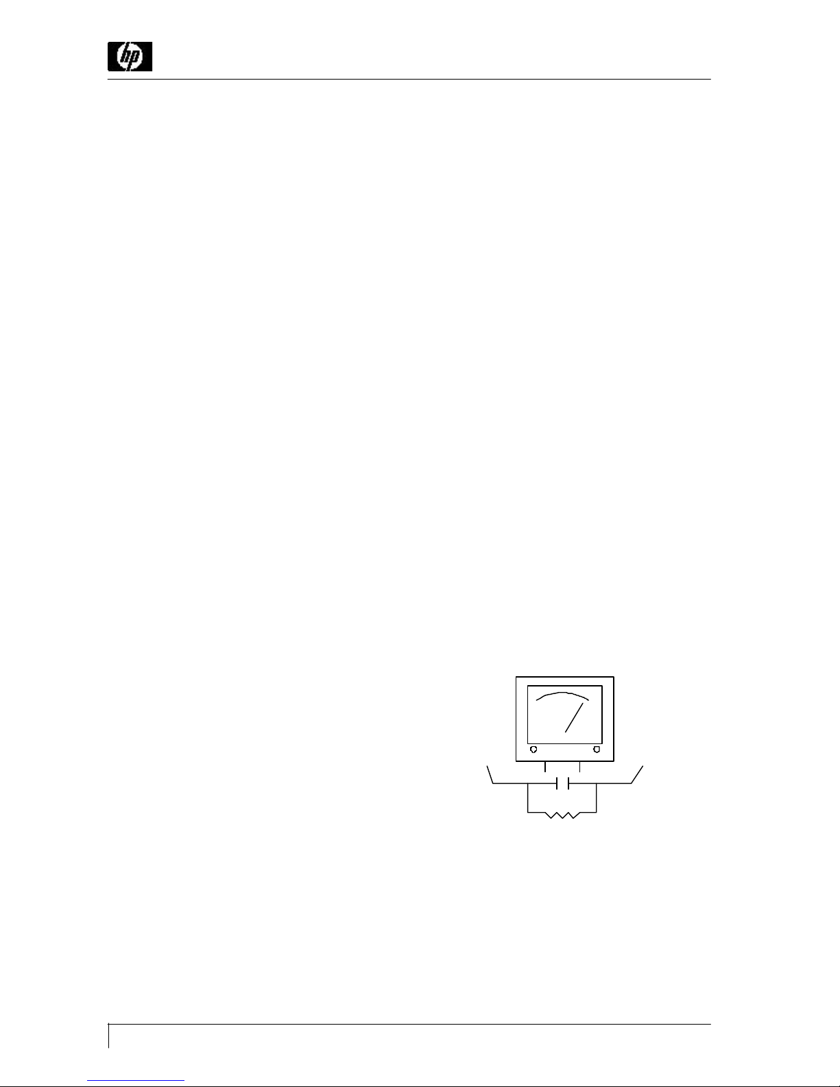
Figure 1-1. Set Up For AC Leakage Current Check
To known
earth ground
1500 ohm 10 watt
0.15ufd
To exposed metal
cabinet part
Page 5
Page 3
HP S7500/MV7500/ CV7500
1-1-3 Product Safety Notices
Many elect rical and mechanical parts in this chassis have special safety-related characteristics which are
often not evident from visual inspection, the protection afforded by them may not be obtained by replacing
them wit h components rated for higher voltage, wattage, etc. Before replacing any of these components,
consult t he Recommended Spare Parts List given at the end of this manual. Any of the replacements that do
not provide the same safety characteristics may result in shock, fire, X-ray emission or other hazards.
1-2 Servicing Precautions
Warn ing: An el ectrolytic capacitor installed with the wrong polarity might explode.
Caution: Before performing servi cing covered by this service manual, read and follow the Safety Precautions
section of this manual.
Note: If unforeseen conflict between the fo llowing servicing precautions and any of the safety
precautions, always foll ow the safety precautions
1. Follow cl osely the servicing precautions printed on the monitor cabinet and chassis.
2. Al ways unplug the AC power cord from the AC power source before removing or installing any component
or assembly, disconnecti ng PCB plugs or connectors and connecting a test component in parallel with a
capacit or.
3. When repl acing parts or circuit boards, clamp the lead wires around the component before soldering.
4. When replacing a high wattage resistor (>0.5W metal oxide film resistor) in the circuit board, keep the
resistor about 1 cm (1/2 inch) away from the ci rcuit board.
5. Keep wires away from the high vol tage or high temperature components.
6. Keep wires in their ori ginal positions so as to minimize interference.
7. Al ways connect a test instrument’s ground lead to the instrument chassis ground before connecting the
posit ive lead; always remove the instrument’s ground lead last.
After put ting the rear cover back and make sure the monitor is working properly, the Hi-Pot &
Ground Conti nuity tests MUST BE performed before the monitor is returned to user.
1-3 Hi-Pot Test
1. T est Equipment
Puncture t est model PM5530 ADT or KIKUSU TOS-8750 voltage tester or equivalent approved equipment.
Not e : The test equipment must be calibrated in regular period.
2. T est Setup
a) Apply volt age : DC 2100 VDC
b) T est duration : 3 seconds
c) Cut off current should be set to 3 mA
3. T est Procedure
a) Unplug power cord from AC source.
b) Put the power swi tch of the monitor in the “ON” position.
c) Leave signal cable un-connected.
Page 6

Page 4
HP S7500/MV7500/ CV7500
d) Plug monitor power cord to the Hi Pot tester terminals.
e) T urn on tester and watch the indicator or beeper.
f) If the indicator lamp lighten, or beeper beeps, the test fails.
1-4 Ground Continuity Test
1. T est Equipment
AC low ohm t ester TOS-6100 or equivalent approved equipment.
Not e :The test equipment must be calibrated in regular period.
2. T est Setup
a) T est duration : 3 seconds
b) Set current limit at 25 A
c) The grounding resist ance must be less than 0.1 ohm.
3. T est Procedure
a) Plug the monitor power cord to the tester terminals.
b) Make sure all connections are wel l-contacted.
c) T urn on monitor power and tester power.
d) Press “T est” button.
e) If green light shows up, means test OK.
If red l ight shows up, means test fails.
f) If the Tester has a digital display, the resistance value must not exceed 0.1 ohm.
Not e :Be sure not to touch the metal portion of the signal cable head during testing.
Page 7
Page 5
HP S7500/MV7500/ CV7500
2 Product Specifications
2-1 Specifications
Not e: Above specifi cations are subject to change without prior notice.
Picture Tube
17-inch (16-inch Visual image area), sloted mask, 90 degrees
deflection, dot type black matrix, medium short persistence
phosphor, dark tint, non-glare/ anti-static screen,
0.27 mm dot pitch for E1770NSL/T and 0.25mm dot pitch for HP
S7500/MV7500/CV7500
Scanning Frequency
VGA, Super VGA, 1024x768@60/70/75/85 Hz
1280x1024@60Hz
Maximum Resolution 1280 dots (H) x 1024 lines (V) @60Hz refresh rate
Display Area 306 mm (H) x 230 mm (V) typical
Display Characters 80 char. x 60 rows on a 10 x 10 matrix
Display Colors Analog
Input
Unlimited Colors
Synchronizatin Signals Separate Sync: horizontal/vertical, TTL, positive or negative
Synchronization
Frequencies
Horizontal : 30 to 70 kHz
Vertical : 50 to 140 Hz
Signal Connectors 15-pin, D-shell connector
Video Signals Analog : 0.7 Vp-p, RGB positive
Power Input 75 Watts (maximum) AC rated voltage, 100VAC to 240VAC
Misconvergence Center Area : < 0.3 mm; Corner Area : < 0.4mm
User Controls Power On/Off, Contrast, Brightness, Horizontal Size, Horizontal
Position, Vertical Size, Vertical Position, Pincushion, Trapezoid,
Rotation, Color temperature, Language, Display Frequency,
Degauss, Recall, H. Moire,
V. Moire
Service Controls PWB-1709
PWB-1707 : power voltage adjust (VR801)
Preset Modes 8 (see Table 2-2. Timing Chart)
Environmental
Considerations
Operation temperature : 10oC to 40oC ambient
Operation Humidity : 20% to 80% ambient
Storage temperature : -40oC to 65oC ambient
Storage Humidity : 10% to 90% (non-condensing)
Altitude : Non operating 40,000 feet sea level
operating 10,000 feet sea level
Page 8
Page 6
HP S7500/MV7500/ CV7500
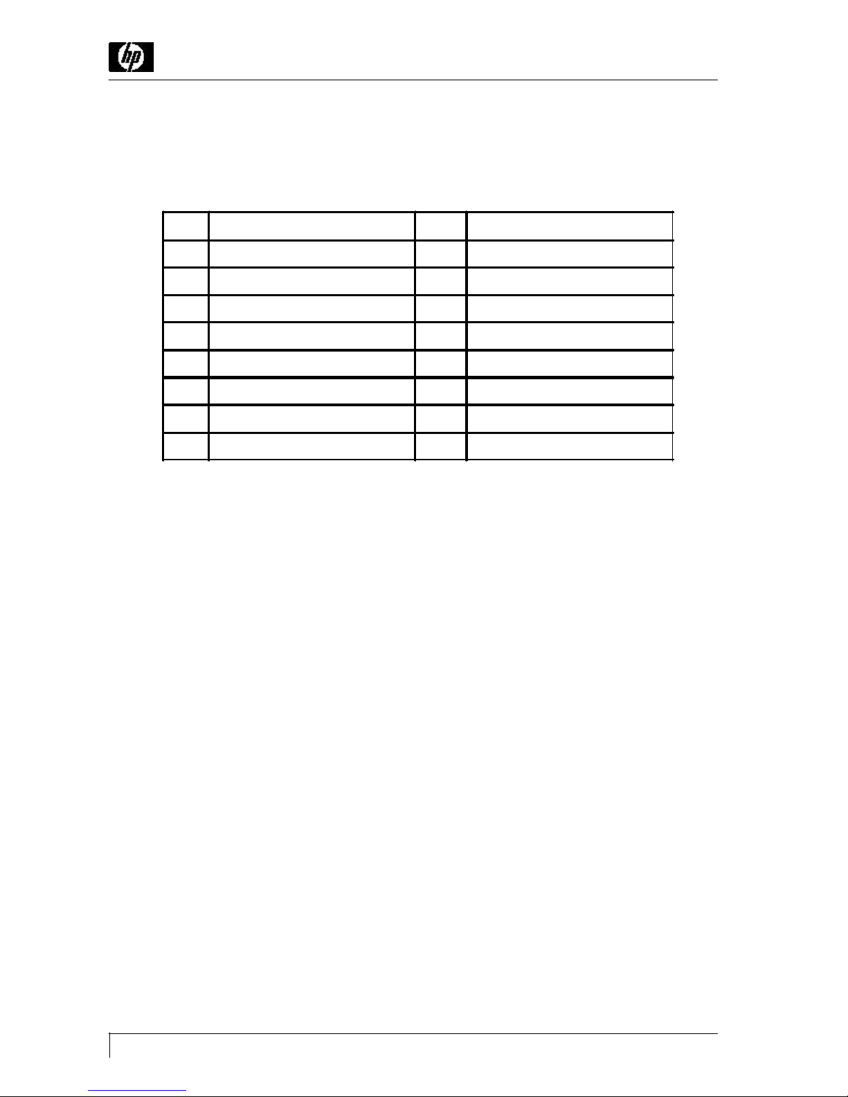
2-2 Signal Cable Pin Connections
Table 2-1. Signal Cable Pin Assignment
Note * This pin i s used for selftest detection. Connect this pin to ground at the PC end.
** For PC 99: This pin will provide +5V from PC side.
Pin Signal Pin Signal
1 Red video 9** +5V
2 Green video 10 Digital Ground
3 Blue video 11 Ground
4 Ground 12 SDA
5* NC 13 H-Sync
6 Red ground 14 V-Sync/VCL
7 Green ground 15 SCL
8 Blue ground
Page 9
Page 7
HP S7500/MV7500/ CV7500
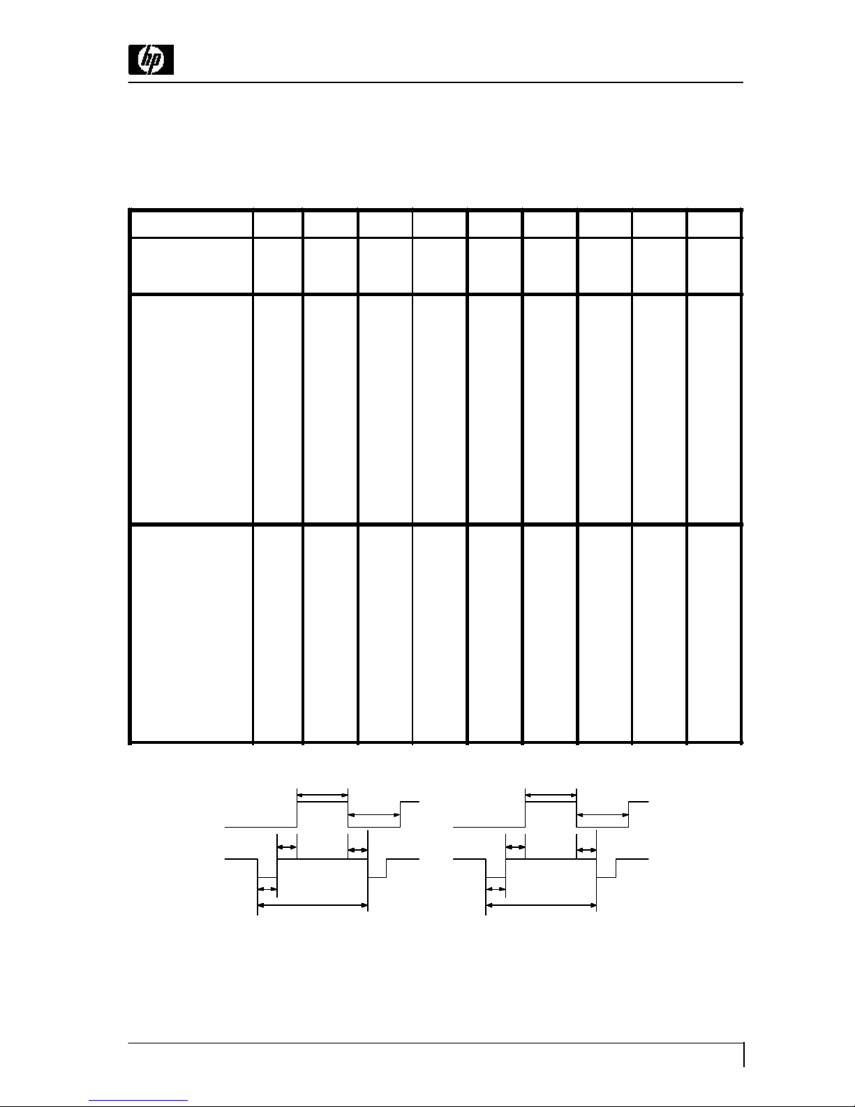
2-3 Timing Chart
This section describes the ti mings that the computer industry recognizes as standard for computer-generated
vi deo signals.
Table 2-2. Timing Chart
H.Parameters:
A: Peri od B: Blanking T ime
C: Sync W idth D: Back Porch
E : Active Time F : Front Porch
V.Parameters:
G: Peri od H:Blanking T ime
I: Sync W idth J: Back Porch
K: Act ive Time L : Front Porch
Seperate Sync
Horizontal
Video
C
D
E
Sync
A
B
F
Vertical
Video
I
J
Sync
G
H
L
K
Mode 1 2 3 4 5 6 7 8 9
H. Dots 640 720 640 640 800 800 1024 1024 1280
V. Dots 480 400 480 480 600 600 768 768 1024
H-freq (kHz) 31.47 31.47 37.5 43.27 46.8 53.67 60.02 68.68 63.98
Sync Polarity - - - - + + + + +
A period us 31.78 31.78 26.666 23.11 21.333 18.63 16.66 14.56 15.63
B Blanking us 6.356 6.356 6.349 5.33 5.172 4.409 3.657 3.725 3.778
C Sync us 3.81 3.81 2.032 1.556 1.616 1.138 1.219 1.016 1.037
D B.P. us 1.907 1.907 3.81 2.22 3.232 2.702 2.235 2.201 2.296
E Active us 25.42 25.42 20.37 17.78 16.162 14.22 13 10.836 11.852
F F.P. us 0.636 0.636 0.51 1.556 0.323 0.569 0.203 0.508 0.444
V-freq (Hz) 59.95 70.08 75 85 75 85 75.03 85 60.02
Sync Polarity - + - - + + + + +
O Period ms 16.68 14.27 13.3 11.76 13.333 11.76 13.33 11.77 16.661
P Blanking ms 1.43 1.557 0.533 0.67 0.533 0.578 0.533 0.582 0.656
Q Sync ms 0.064 0.064 0.08 0.069 0.064 0.056 0.05 0.044 0.047
R B.P. us 1.02 1.08 0.427 0.578 0.448 0.503 0.466 0.524 0.594
S Active us 15.25 12.71 12.8 11.09 12.8 11.18 12.8 11.18 16.005
T F.P. us 0.35 0.413 0.027 0.023 0.021 0.019 0.017 0.015 0.016
Page 10

Page 8
HP S7500/MV7500/ CV7500
2-4 Power Saving Function
Note: The monitor will be driven into “Power Saving” mode by the control signal from the display
controller, as indicated by t he amber-color power LED.
Table 2-3. Power Saving Function
State Power
Consumption
LED
Light
ON Normal* Green
Active
OFF
<5 watts Amber
The power savi ng states will be kept until a control signal has been detected or the keyboard or mouse is
act ivated. The recovery time from Active OFF state back to ON state is around 10 seconds.
* For power consumpti on : 75W Max. (@ 230V AC, preset size and maximum light output condition)
2-5 TCO Version (Optional)
The monitor meets the TCO 95/ 99, NUTEK energy saving, electric and magnetic field requirements.
Al so it is compliant with TCO 95/TCO 99 labelling scheme.
The emission from magnet ic and electric field must comply with the limits specified by the Swedish Board
for M easurement and Testing, commonly known as MPR 1990 recommendations. These limits are summarized in the T able 2-4.
Table 2-4. TCO 95 Emission Requirements
VLF/TCO ELF/TCO
Magnetic Field 25 nT 200 nT
Electric Field 1 V/m 10 V/m
Frequency Range 2~400 kHz 5~2000 Hz
Value RMS RMS
Distance 30 cm 30 cm
Electrostatic
Potential
+/- 500 V +/- 500 V
The moni tor is designed with selected CRT and carefully routed wires around CRT, make sure exactly the
Page 11

Page 9
HP S7500/MV7500/ CV7500
same routing scheme is used when doing CRT replacement.
2-5-1 TCO 95 Versi on (Optional)
The T CO 95 scheme is for international and environmental labelling of personal computers. The labelling
scheme was developed as a joint effort by the TCO (The Swedish Confederation of Professional Employ
ees), Naturskyddsforeningen (T he Swedish Society for Nature Conservation) and NUTEK (The National
Board for Industry and T echnical Development in Sweden).
1)`Scope
TCO 95 t ouches on ergonomic qualities, emissions (electrical and magnetic fields), energy efficiency and
ecology (with demands for environment al adaptation for both the product and the production processes at
the manufact uring plant).
2) Envi ronmental Requirements
The moni tor abides by the environmental demands concerning restrictions on the presence and use of
heavy metals, bromi nated and chlorinated flame retardants, CFCs (freons), and chlorinated solvents, among
ot her things. The monitor is also recyclable.
3) Energy Requirements
The monitor also fol lows the energy requirements that, after a certain period of inactivity, the monitor shall
reduce i ts power consumption to a lower level in one or more stages.
4) Others
The monit or meets the strict environmental demands for the reduction of electric and magnetic fields,
physical and visual ergonomics and good usabil ity.
T able 2-5. TCO 95 Visual Ergonomics
Feature Standard Description
Linearity 1% or less Difference in length of columns or rows compared to the
corresponding lengths through the center of the monitor.
Display Luminance 100 cd/m2 (at least)
Luminance
Uniformity
1.7:1 or less The ratio is between the max to min luminance within the
whole active area.
2-5-2TCO 99 Version (Optional)
TCO 99 wi ll append the color temperature and energy efficiency specification, also cover the environmental requirement.
Page 12

Page 10
HP S7500/MV7500/ CV7500
3 Operation Th eory
This is a fully di gital controlled multi-sync color monitor that is compliant with DDC1 and 2B Plug and Play
VES A standard and offers the following main features.
3-1 Main Features
1. Si mplified design with minimum components.
2. The NOVA NT 6865 32 processor-- that has I2C BUS controlled geometri c correction, contrast and
brightness-- offers the functions for: (a) Contrast, (b) Brightness, (c) H-size, (d) H-position, (e) V-size, (f)
V-positi on, (g) Pincushion, and (h) Trapezoid.
In addition, it also offers more functi ons as: (a) Sync. processor, I/P and O/P, (b) Mute, (c) Power saving
- Suspend & Stand-By, (d) P ower saving override, (e) DDC1/2B, (f) I2C Bus for auto-ali gnment through
si gnal cable (g) CS1/CS2/CS3/CS4 for linearity and size compensation.
3. St ores up to 10 factory preset modes and offers 8 user modes. There are 16 function icons at OSD. They
are controlled by 1 2 keys on front panel.
4. Powerful P HILIPS TDA4863AJ A5 and TDA4841 present the following useful functions: (a) Pincushion,
(b) T rapezoid, (c) V-Position, (d) V-Size, (e) Vertical’s “C” and “S” correction -- factory adjust, (f)
Pincushion’s V. position correction, (g) Corner correction -- factory adjust, (h) P incushion unbalance
correction -- fact ory adjust, (i) Parallelogram distortion -- factory adjust, (j) Moire cancellation, (k) X-ray
protecti on, and (l) Full horizontal and vertical auto sync capability.
5. Software controll ed auto shut off function activated if fH < = 29 kHz and fH > = 70 kHz.
6. Full range AC i nput and simplified line filter design.
3-2 Microcontrol Section
1. Thi s monitor uses NOVA NT6865 CPU. It contains a 8051 8-bit CPU core, 512 bytes of RAM used as
working RAM and stack area, 32k bytes of MAS K ROM, 10-channel 8 bit PWM D/A converter, 4channel A/D converters for key det ection saving I/O pins, internal H. sync and V. sync signals processor
provi ding mode detection, and an I2C bus i nterface. When H/V sync through D-Sub signal cable enter pin
41 and pin 42, t he CPU performs frequency / polarity detection and calculate and send to H/V sync OUT.
Then CPU reads the data from I703 and transfer to devi ce 4841 and some DAC in CPU, above operation
takes about 500 ms.
2. There al lowed 8 factory preset modes and 8 user modes. There are 11 functions, Contrast, Brightness, H.
Si ze, H. Position, V. Size, V. Position, Pincushion, and Trapezoid, Rotation, H. Moire, V Moire, all controlled
by OSD icon whi ch can be adjusted by user.
3. The pin 25 and pin 26 are used for AT E function. When CPU receives C6 as slave address, it will operate
in ATE mode which is used for auto-alignment. After alignment the data will be stored in I703.
4. The user control parameters are selected by OSD icons, through 1 & 2 keys, they are detected
by sensing t he voltage through R710, R740, R741, R743, J007, J008 to pin 16 and 17 of I701.
3-3 Deflection Section
1. I2C -- autosync defl ection controller is TDA4841.
2. The TDA4841 is a high performance and efficient solution for autosync monitors. All functions are
control lable by I2C bus. SDA and S CL signals coming from microprocessor feed to pin 12 and pin 13 to
control all functions.
Page 13

Page 11
HP S7500/MV7500/ CV7500
3-3-1 Horiz ontal Section
1. The osci llator is driven by the currents in R419 and R420. The minimum oscillator frequency is determined
by R419 and t he maximum frequency is determined by R420.
2. Hori zontal sync goes into pin 15 through R318. And horizontal flyback pulse goes into pin 1 through R401
from pi n 5 of FBT for HFLB loop.
3. Horizontal driver (pin8) O/P t o Q401 via C410.
3-3-2 Vertical Section
1. Verti cal sync goes into pin 14 through R317.
2. The free running frequency is determined by R301 and C301.
3-3-3 Vertical O/P section
1. The di fferential output currents from pin 13 of Vout1 and pin 12 of Vout2 can be directly coupled to the
vertical defl ection booster pin 1 and pin 2 of TDA4863 AJ.
2. The TDA4863 AJ has two output stages which are current driven in opposite phase and operate in
combi nation with the deflection coil in a full bridge configuration.
3. This IC is powered by two sets of posit ive voltage and one set of negative voltage. (+12V at pin 1, -12V
at pin 4).
3-3-4 E-W/Trapezoid and H. Width Contr ols
1. The horizontal O/P stage uses diode modulator D419, C411, C412, L409 and C418 for East-W est
(P incushion) Trapezoid and H. width controls.
2. The scan current i s determined by B
+
mi nus Vm ( the voltage of C418) values and the pincushion control is
accomplished by OP AMP(KA324) I402 and Q419 by coupling a parabola waveform from pin 11 of
TDA4841. The H. width / corner and trapezoid correct ion are also accomplished by this pin 11. The DC
level control s H. size. The AC level is combined with side pin and trapezoid corners functions.
3-3-5 X-Ray Protec tion
1. T o avoid X-ray hazard, a DC voltage generated at pin 5 of FBT and rectified by D410, C424 and divided
by R404, R406 and R405 come int o pin 2 of TDA4841.
2. If t his voltage is higher than 6.39 V, then TDA4841 will be activated to float HUNLOCK (pin17), H.
DRV( pin 8), B DRV (pin 6), VOUT1 (pin 12), VOUT2 (pi n13). After that all deflection circuit stop
worki ng.
3-3-6 G1, Blanking and Bri ghtness
1. The vertical blanking signal comes from unlock pin 17 of I401. This positive vertical pulses through Q405
ampli fied and converted into negative pulse and sent to G1 for vertical blanking.
2. In protection mode or an out-of- range sit uation HUNLock will send 5 V pulse to CPU pin 30 of I701,
then G1 wil l go down to -150V. During the mode change, Mute acts as same as HUNLock’s.
3-3-7 Contrast Section
1. Contrast i s controlled by I701 through I2C bus to I501 (LM1237) directl y.
2. Beam current is det ected through T402 (FBT) pin 7, C429, R449 and detected voltage feeding into pin 12
of I403 (KA324), R459, R548, C556 to control I501 pin 22 voltage. When I501 pin 22 voltage drops
Page 14

Page 12
HP S7500/MV7500/ CV7500
belo w 4.0 V, the ABL function will happen.
3-3-8 H/V s ize breathing compensation
1. Beam current is sensed as above section (3-3-7 it em 2) and this voltage routes through R451, R468, C470
then through R437 to pin 31 of I401 for H. size compensation.
2. HV volt age is detected through T402(FBT) pin 11. C481, R4F4, R4F8, C430, R411, pin 5, 6, 7 of I403
(KA324) t hen through R302 to I401 pin 21 for V. size compensation.
3-3-9 Dynamic foc us circuitry
The dynamic focus is applied to i mprove the corner focus performance, it includes horizontal and vertical
dynamic focus.
1. Horizont al dynamic comes from Idy current through T403, R434, C448, R428 and feed to FBT dynamic
focus pi n (T401 pin 12).
2. Vert ical dynamic comes from pin 32 of I401 through C315, R309, R326, R322, R323, Q301, R324, R325
and feed to FBT dynamic focus pin.
3-4 Power Supply Section
3-4-1 AC Rectifier
The circuit can accept 90 V to 264 V AC input through D801~D803 bridge diodes and C808 filtering to get
DC 126 V~ 364 V for power conversion in T802.
3-4-2 Line Filter
It consists of C803, T801, C804, C805, C808, C819, C807, C817 and meets EMI regulation.
3-4-3 Power LED Status
1. The LE D has 3 leads with common cathode to emit green and amber color light for different power
saving st ates. It is controlled by CPU.
2. Normal : Green light
Amber L ED is off because CPU pin 29 is 1.96V and pin 24 is 0.45V, only green LED is turned on.
3. Off Mode : Amber li ght
CP U pin 24 is 1.87V and pin 29 is 0.46V, then green is off and amber is illuminated.
3-4-4 Auto Degaussing
When S 801 turns on, pin 27 of I701 will send a signal to Q802 and turns on RL801 for degaussing. After 4
seconds, it wil l turn off RL801 automatically.
3-4-5 PWM Control
1. Start Up
The I801 (5S 0765C) gets power from R807, R808, C830 and pin 3 voltage reaches 15 V for starting up.
The I801 st arts oscillation at 20 kHz, pin 1 output to drive T802. Switching on, R819 set up an 15 V to
keep I801 working t hrough D809 auxiliary voltage.
Page 15

Page 13
HP S7500/MV7500/ CV7500
2. Regul ation
The DC O/P voltage is proportional to the auxi liary voltage, so I801 pin 4 senses the feedback voltage
from the divi der D806, R809, C810, VR801, Q803, Q801 and R821 to compare with the built-in 1.5 volts
reference volt age for error amplifier operation. Finally pin 6 can modulate the different duty cycle by
VR801 set ting to achieve regulation purpose.
3-4-6 Synchroniz ation
1. Normal M ode
The sync pul se from FBT (31 kHz~69 kHz) via R812, R811 and C815 to pin 5 of I801 to keep I801
synchronized wi th horizontal sync input frequency.
2. Power Saving Modes: St andby/Suspend
Because there is no pulse from FBT , so the free-run frequency SMPS works at 20 kHz by I801 itself.
3. Overri de
The horizontal free run frequency is about 63.2 kHz under override condition, SMPS is synchronized to
this frequency.
3-4-7 O.V.P.
If the auxiliary volt age is higher than 25 volts makes pin 3 of I801 is limited to have the OVP activated.
3-4-8 O.P.P.
The excess current of T 802 through I801 pin 1, 2, make Vs>1.1V internal of I801, then limite the power.
3-4-9 St ep Up Power Supply For FBT
1. The B+ of F BT is proportional to horizontal frequency, that is the higher frequency, the higher voltage.
The basic voltage is 58 volt s from T802 pin 10 via L811, D813, C824 and the gate control of Q451 comes
from I401 pin 6 via Q450, Q434, Q435 and R4E5. T he duty cycle is controlled by I701 pin 23 (PWM pin
Adj.) vi a R719, C741, R4F6, R4F5, R4F1.
2. The regulat ion and boost up (from 68 V to 160 V or more, on demand). The H.V. is set at 25 kV (zero
beam) by I701 pin 23 which senses the secondary O/P from FBT . The booster comprises Q451, L410,
L411, D450, C425 and T802 to offer the required B+ for different frequency modes.
3-5 Video Amplifier Section and OSD (On Screen Display) function
1. RGB signal i nputs are terminated by R501, R531 and R561 then pass through the coupling capacitors
C503, C533 and C563 to IC501 L M1237 preamplifier.
2. The amplifier RGB si gnals (0~3 Vpp) are adjusted by I2C bus, I501 pi n 23 is for clamp pulse which comes
from pin 16 of TDA4841 t o set up equal clamp level.
3. The pre-amp vi deo stage is amplified by I501 (LM1237/NT6812), it’s including OSD function and control
by I701 pin 12, 13 (I2C).
4. The video output stage 15 is ampli fied by I502 (LM2469/LM2466).
5. The RGB cat hodes cut off are adjusted by I503 (LM2480) pin 8, 7, 6, which comes from I501 pin 16, 15,
14 to adjust cut iff voltage level by I2C bus.
6. Under overri de condition, “NO SIGNAL” will show up on the screen.
Page 16

Page 14
HP S7500/MV7500/ CV7500
4 Alignments an d Adjustments
This secti on of the service manual explains how to make permanent adjustments to the monitor settings.
4-1 General Adjustments
4-1-1 Adjust ment Conditions
a) Power Supply
Apply AC 115 V or 220 V
b) W arm-up Time
The monitor must be powered on for 15 minutes before starting any alignment, but requires 30 minutes of
warm-up t ime for convergence adjustment.
c) Si gnal Input
1. Vi deo: RGB Analog, 0.7 Vp-p, positive
2. S ynchronization: Horizontal and vertical TTL signal, separate, positive or negative
3. All adjustments shoul d be made using a signal of FH = 68.68 kHz, FV = 85 Hz, unless otherwise
defined.
4-1-2 Equipme nt Requi red
The following equipments are necessary for adjustment procedures:
1. Vol t-ohm-A meter (Sanwa FD-750C or equivalent)
2. 30 kV hi gh voltage probe (HP34111A)
3. Oscil loscope (TEK2235 or equivalent)
4. Mi nolta Color Analyzer II
5. Signal generator (IBM P C with proper display cards or Chroma 2000)
6. Screwdri ver
4-1-3 Swi tching Power Supply and Regulator Adjustment
a. The regul ated B+ control has been preset in the factory and needs no adjustment. However, if any repair
is made on t he power supply section, the following readjustment procedures are recommended:
1. Al low the monitor to warm-up for about 15 minutes.
2. Apply VGA (1024 x 768 @ 68.68 kHz/85 Hz) signal to the monitor.
3. Connect a DC voltage meter to TP001 (on the Main board), and adjust VR801 for 11.6 ± 0.1 Vdc
4. If a fuse is broken during adj ustment, remember to replace it with the exact same type of fuse.
b. If necessary, foll ow the following procedures to enter the factory mode.
1. Press bot h 1 key and 2 key si multaneously then power ON.
2. After turn the power off, this moni tor will go back to normal mode.
Page 17

Page 15
HP S7500/MV7500/ CV7500
4-2 Alignment Procedures
4-2-1 High Voltage Adjust ment
CONDITION
Press 1 and 2 buttons simultaneously when switching the power “On”.
Di splay image : No video (68.68kHz Mode)
PROCEDURE
Connect DC met er to TP002 and adjust HV (i)
R802 t o obtain a DC voltage of -173.5 ± 0.2 V DC (Sampo FBT) or -172.5 ± 0.2V DC (LCE FBT) for CPT
CRT M41AGE93X46 (TCO) or M41AGE83X46 (MPRII) .
4-2-2 Scree n and White Balance Adjustment
CONDITION
Press 1 and 2 buttons simultaneously when switching the power “On”.
Di splay image : No video (68.68kHZ Mode)
PROCEDURE
1 Rast er color setting
1-a. Set Brightness max. to 77, G1 to 60 (OSD cursor) and 530 ± 5 at G2, cursor.
1-b Adj ust R and B cutoff to min.
1-c Adj ust G cutoff to about 0.45FL
1-d Adj ust B cutoff to get y=298 ± 5, R cutoff to get x=283 ± 5 and Y=0.65 ± 0.05 FL.
1-e Adj ust Brightness cutoff to raster 0.01-0.02 FL.
CONDITION
Di splay image : 50 mm x 50 mm white block pattern
PROCEDURE
1 55000K col or temperature setting
1-a. Set Brightness to cutoff and Contrast to maximum.
1-b Move cursor on OSD t o choose color temperature icon.
1-c. W ith green block pattern, adjust G gain to get Y about 32FL.
1-d Adj ust R.B. gain to get x=333 ± 5, y=348 ± 5; and Y=40 ± 0.5FL
2 65000K col or temperature setting
2-a. Set Brightness to cutoff and Contrast to maximum.
2-b Move cursor on OSD t o choose color temperature icon.
2-c. W ith green block pattern, adjust G gain to get Y about 32FL.
2-d Adj ust R.B. gain to get x=313 ± 5, y=329 ± 5; and Y=43 ± 0.5FL
3 93000K col or temperature setting
3-a. Set Brightness to cutoff and Contrast to maximum.
3-b Move cursor on OSD t o choose color temperature icon.
3-c. W ith green block pattern, adjust G gain to get Y about 32FL.
Page 18

Page 16
HP S7500/MV7500/ CV7500
3-d Adjust R.B. gain to get x=283±5, y=297±5; and Y=46±0.5FL
4 Ful l white ABL setting
CONDITION
Di splay image : full white pattern
4-a Set Brightness to cutoff and Contrast to maximum.
4-b. Adjust ABL to Y=31FL ± 0.5FL.
4-c. Check the whit e balance at 5FL and 28FL.
4-d. Repeat all the procedures in 4-2-2 section until the best white balance is obtained.
4-2-3 Foc us Adjustment
CONDITION
Di splay image : “me” character pattern (68.68 kHz Mode)
PROCEDURE
1. Set Brightness to cutoff and Contrast to maximum.
2. Adj ust focus 1 at T402 (static focus VR) to make vertical line clear.
3. Adj ust focus 2 at T402 (static focus VR) to make horizontal line clear.
4. Repeat above procedures to get best focus.
4-2-4 Static Convergence Adjustments
St atic convergence involves alignment of the red, blue and green lines in the center area of the display.
Not e : The monitor requires 30 minutes of warm-up time for convergence adjustment.
CONDITION
Display image : Crosshatch pattern
W arm-up Time : 30 minutes
PROCEDURE
1. Set brightness and contrast to display a well-defined pattern.
2. Ensure the convergence magnet ri ngs are correctly positioned on the CRT.
Figure 4-1. Convergence Magnets on the CRT
+
8 76 5 4 3 2
10
1
11
CRT
FRONT
P
9
1) Setup Bolt 2) Bow Magnet 3) Band 4) 2-Pole Magnet
5) Spacer 7) Spacer
9) Holder
6) 4-Pole Magnet
8) 6-Pole Magnet
11) Tabs10) Band
Page 19

Page 17
HP S7500/MV7500/ CV7500
4-2-5Degaussing
Degaussi ng is required when poor color impurity appears on the screen. This monitor uses an automatic
degaussing circuit that is activated when t he power is on. The automatic degaussing will be fully functional
again after the monit or has been in operation for 20 minutes.
The degaussing effect is confined to the picture tube since the coi ls are mounted at the back of the tube.
Should any part of the chassis or cabinet becomes magnetized, it is necessary to degauss t he affected area
wi th a manual degaussing coil.
4-2-6Manual Degaussing
1. Appl y line voltage to the degaussing coil and move it in a rotary motion over the front, sides, and top of the
monit or. The coil should be kept away from the rear of the monitor to avoid damaging the magnetic neck
component s.
2. Sl owly rotate and move the coil away from the monitor to about 6 feet beyond the point where no effect
on the CRT will be noticeable.
For proper degaussi ng, it is essential that the field be gradually reduced by moving the coil slowly away from
the monitor. The degaussing coi l must never be shut off or disconnected while near the monitor, as this would
int roduce a strong field instead of canceling the effect of the stray fields.
3. Rotat e the individual rings of 4-pole convergence magnets by changing the spacing between the 2 tabs to
converge the vertical red and blue lines at t he center of the screen.
4. Rotate the pair of rings of 4-pole convergence magnet s by maintaining spacing between the 2 tabs to
converge the horizontal red and blue l ines at the center of the screen.
5. Rotat e the individual rings of 6-pole convergence magnets by changing the spacing between the 2 tabs to
converge t he vertical red, blue and green lines.
6. Rotate the pair of rings of 6-pole convergence magnet s by maintaining spacing between the 2 tabs to
converge the horizontal red, blue and green l ines.
7. Repeat the steps from 3~ 6 until the best convergence is obtained.
Figure 4-2. 4-pole and 6-pole Magnets Movement
Not e : The 4-pole magnets and the 6-pole magnets interact, making dot movement complex.
Blue Red
Blue
Red
Red/
Blue Green
Red/
Blue
Green
4-pole magnets
movement
6-pole magnets
movement
Page 20

Page 18
HP S7500/MV7500/ CV7500
5 T roubleshooting
5-1 No Raster
Check voltage of
cathode, heater,
Grid 1, Grid 2, etc.
Check I401,
I703, R719, C741,
R4F6, R4F5, R4C4
Check
I801, R807,
R808, Q801,
Q802, ZD802,
VR801
Check D801,
D802, D803,
D804, T801,
R804, F801
Yes
No
Normal
(68 V, 31.5 kHz)
Short Circuit
at load?
Measure
voltage of B+ at
T402 pin 2 on
PWB-MAIN
No Raster
0 V
High
(75 V or more)
Check DC
B+ line, Q451,
Q402, T402
Yes
Check voltage
of C808
No
Page 21

Page 19
HP S7500/MV7500/ CV7500
5-2 OSD Abnormal
Put on
I502
Replace them
No
Check I502 pin 9, 4
is 5V and pin 5, 10, 7,
8 missing?
Check R517, L514,
R527, R523, R524
OK?
OSD Abnormal
Yes
No
No
Replace it
Yes
Yes
Check P502
OK?
Replace I502
Page 22
Page 20
HP S7500/MV7500/ CV7500
5-3 Function Key Abnormal
Put on
I701, I703
Replace X701
No
Check I701 and
I703 missing?
Power
ON/OFF again and
check X701, oscillator
OK?
Function Key Abnormal
Yes
No
No
Replace I703 or do
ATE again
Yes
Replace I701 and check
uP OK?
Yes
Check
I703 EEPROM content
OK?
No
Replace I705, D703
Check
pin 5 of I701
is 5V?
Replace I701
Yes
Check
R775, R735
Yes
No
Page 23

Page 21
HP S7500/MV7500/ CV7500
5-4 No Vertical Scan (Raster is one horizontal line)
Ckeck or replace
I301.
Check R312, R307,
R306, R313
Yes
Check I301 voltage of
pin 1 is 12V, pin 4 is
-12V
Check
pin 5 O/P waveform at
I301
No Vertical Scan
No
Yes
No
Check
pin 6, 7 of I301
waveform
Still no vertical scan
Check or replace CRT
Replace I401
No
Page 24

Page 22
HP S7500/MV7500/ CV7500
5-5 Out of Horizontal Synchronization
5-6 Out of Vertical Synchronization
Check or replace
the signal cable or
H. sync pin 41
of I701.
Check or replace
I401, C406
Yes
Horizontal
sync present at
pin 15 of I401
Check
I401 pin 8 H. output
frequency & pin 29
waveform
Out of Horizontal
Synchronization
No
Yes
No
Check Q401,
T401, Q402,
R424, D401
Check signal
cable & V. sync
pin 42
of I701.
Check or replace
I401,
Yes
Vorizontal
sync present at
pin 14 of I401
Check
I401 pin 24 waveform
Out of Vorizontal
Synchronization
No
Yes
No
Check I401 pin 13 & pin
14.
Page 25

Page 23
HP S7500/MV7500/ CV7500
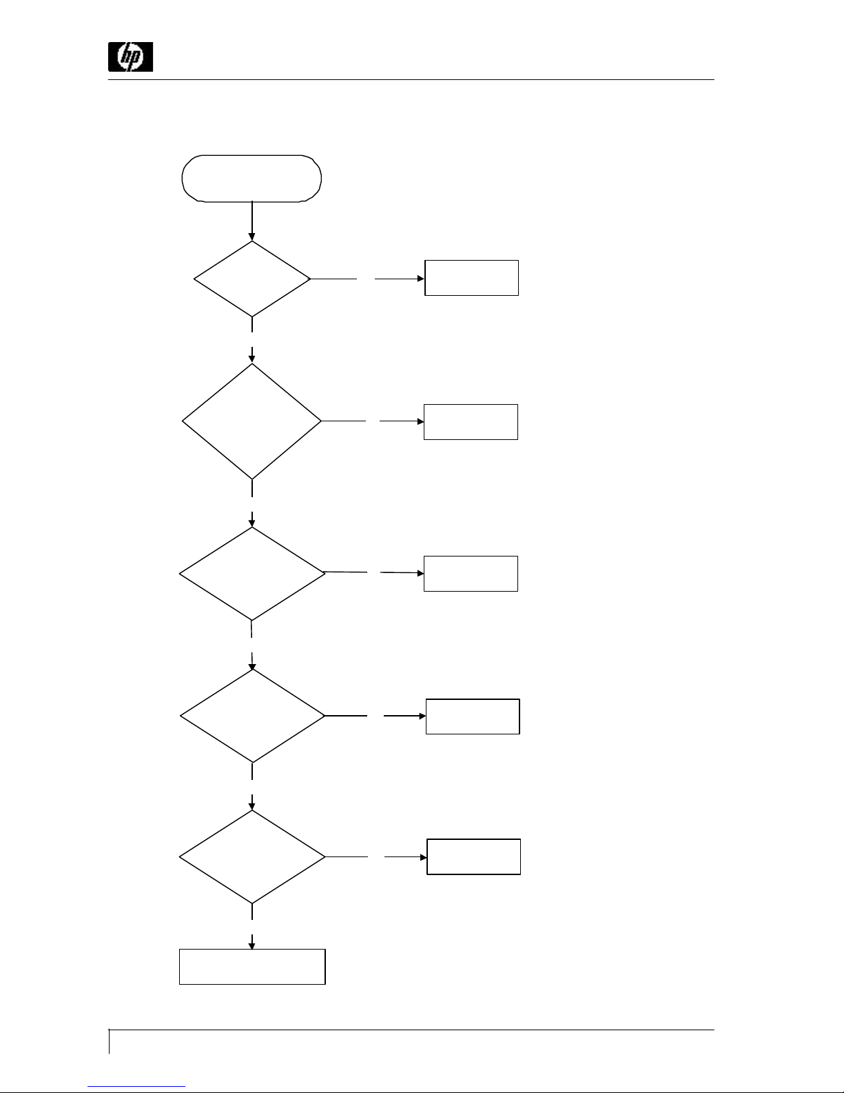
5-7 R.G.B. Video Amplifier Abnormal
5-8 Blank EEPROM Trouble-shooting:
Description o f functions for models under E1770 series EEPROM DATA AUTO-RELOAD
The function allows plant staff to pre-write and customer service personnel to use blank EEPROM
through the pre-write EEPROM function whenever the CPU is implemented. The met hod of operation
is as follows:
Fi rst, start after HP S7500/MV7500/CV7500 turns to (<&>) KEY. At this point of time, the CPU is capable
of detecting the fi rst 8 DATA of each page that EEPROM contains. When the reading goes to 00H or FFH,
the EE PROM PAGE will turn to blank; instead, the pre-set value is being written into the EEPROM through
CP U. Otherwise, it shall be deemed an effective value and that the pre-write function shall not be activated.
Note: The pre-wri te operation is only used in the service operation, if the EEPROM becomes faulty, we
need to repl ace it with a new one, but, to enable the adjustment ( geometry, color temperature, .. etc ) we
have to put in some " factory preset values " so that we can have a good start point, this is what we call "
pre-wri te " operation.
Check or replace the
signal cable or I501
Yes
Check
waveform at I501 pin 5, 6
and 7
Check
I502 pin 1, 2 and 3 collector
voltage (normally about
70V) & waveform
RGB Video AMP Abnormal
Yes
No
Yes
No
Check I901
Video signal present at the
pin of the CRT R.G.B.
Cathode
Defective cut-off circuit
(DC restore) I503
Page 26

Page 24
HP S7500/MV7500/ CV7500
6 Recommended Parts List
Not e:1. The components identified by “ “ mark are critical for X-ray safety. Replace these with
exact ly the same parts specified.
2 . There is only OTP IC at the model beginning (FPR stage or before). When it put in mass
production and there must be Mask coming out. If you have spart parts need, please use BOM
to get the l ast release part number and related information.
No. Location Part Number Description
1 Q401 6421002705 TR NPN KSD1616A G TA
2 C808 6312615109 ALU uF 150 400V F 85C 25x35
3
D801 D802
D803 D804
6412025607 DIODE LT2A06 T52 2A/800V
4 D814
6412020022 (S0)
6412021702 (S1)
DIODE FE30-02BXF06
5 D810 6412004117 DIODE UF2004M 2A/200V 50 nS
6 D815 6412002617 DIODE UF3002M 3A/100V 50 nS
7 D817 6412024404 DIODE HER106 1A/600V 50 nS
8 F801 6851504053 FUSE TIME LAG H-BRK 4A/250V
9 I301 6442026401 IC TDA4863AJ 7P (PHILIPS)
10 I401 6442030000 IC TDA4841 32P SDIP (PHILIPS)
11 I501 6442031503 IC LM1237 24P SDIP (NS)
12 I502 6442034900 IC LM2466 9P NS
13 I503 6442029901 IC LM2480 8P NS
14 I701 6448017800(OTP) IC NT6865 42P PDIP NOVA
15 I703 6448015730 IC MTV24C08 (ATC)
16 I705 6442000875 IC KIA78L05 (SAMSUNG)
17 I801 6442031600 IC 5S 0765C 5P FAIRCH
18 L404 6111274130 COIL CHOKE 2.7mH K DR8x10
19 L405 6119008400 COIL LINEAR
20 L409 6111155133 COIL CHOKE 150uH DRWW 14x15 LY3B
21 L410 6111155138 COIL CHOKR L=150uH K DRWW 14x15
22 Q402 6421004900 TR NPN 2SC5387
23 Q405 6422002925 TR NPN HBF422T/B TO-92 TAPING
Page 27

Page 25
HP S7500/MV7500/ CV7500
No. Location Part Number Description
24 Q419 6422006000 TR NPN 2SD2012 TO-220(IS)
25
Q420 Q421
Q430
6426010510 (S0)
6426010500 (S1)
FET N-CHNL IRF630MFP/IRFS630A
26 Q451 6426006300 FET N-CHNL IRFS634A FAIRCH 11d
27 R803 6203080022 POSISTOR & OHM DGC2D8ROM
28 R804 6201100012 THERMISTOR 10 OHM 3A P=5 UEI
29 R802 R803 6221127852 MOF OHM 0.27 1W J HOR
30 T401 6135000801 XFRMER HOR DRIVE THD-1008A EI19
31 T402
6133070230
6133070240
FBT TFB-7023 FEA9 SAMPO (S1)
FBT TFB-7024 CF2001 LIEN CHANG (S0)
32 T403 6136001800 XFRMER DYNAMIC TDF-1018 EI19LSE
33 T801 6138001603 LINE FILTER TLF-1016C 16mH LSE
34 T802
6131042221
6131042231
XFRMER PWR TPW-1084A ERL35 LSE (S0)
XFRMER PWR TPW-1084A ERL35 HJC (S1)
35 X701
6449006900 (S1)
6449006910 (S0)
CRYSTAL 12.000 MHZ 49U 30PF TOP
Page 28

Page 26
HP S7500/MV7500/ CV7500
7 Block Diagram
RG
R
GG
G
BG
B
I501
PRE AMP
LM1237
R
G
B
LM2480
R, G, B
BUFFER
&
DC
RESTORE
I502
Video AMP
LM2469
LM2466
LED
SCL
SDA
I701
NT6865
H
V
I401
TDA4841
SCL 1
KEY
CONTROL
S702
POWER
DEL
CKT
E2PROM
I703
DEG
CKT
LINE
FILTER
BRIDGE
DIODE
5S0765C
I801
SMPS
LOW VOLTAGE
DROP DOWN
POWER
O/P
TRANS
T802
VERTICAL
O/P
I301
BLANKING
CKT
BRIGHTNESS
CONTROL &
SPOT KILLER
H
DRIVER
BRIGHTNESS
H
OUT
DIODE
MODULATE
FBT
STEP
UP
CKT
D.Y
XRP
80V
-150V
650V
6.6KV
+V
-V
-H
+H
P502
P501
25.6KV
VTTL
GND
VIDEO 5 V
GND
O/R
11.7V
Q811
TDA4863J
5V
H
V
SG
SDA
SCL
O/R
SDA 1
V
H
dynamic
foucus
600V
G1
ABL
CLBL
HFLB
SDA1
SCL1
SW5 V
5V
R
G
B
HFLB
ABL
R
G
B
R432
Vertical Focus
7V
-12V
I705
78L05
R DAC
G DAC
B DAC
GND
P503
6.3V
GND
GND
80V
11.6V
G1
SDA
SDA
SCL
SCL
SW 5 V
5V
Q510
80V 11.6V
5V
Rotation
Q820
Q811
Page 29

LITE-ON TECHNOLOGY CORP.
5 F, No. 16, Sec. 4, Nanki ng E. Road, Taipei, Taiwan
T el: 886-2-25706999 Fax: 886-2-25706888
URL:/ / www.liteontc.com.tw
Pri nted in Taiwan
 Loading...