

Page 1
~--------------------HEWLETTiPPACKARD--------------------~
OPERATING
7970B/7970C
DIGITAL
AND
MAGNETIC
TAPE TRANSPORT
Prin ted-Circuit Assemblies:
07970-60481, Series 1101
07970-61010, Series 1323
07970-61020, Series 1229
07970-61080, Series 1042
07970-61150, Series 1049
07970-62172,Series1322
07970-62173, Series 1329
07970-62086, Series 1013
07970-62089, Series 1206
SERVICE
PART
2
TAPE
MANUAL
UNIT
07970-90383
Copyright
11000
Wolfe
HEWLETT-PACKARD
Road,
Cupertino,
COMPANY
California
95014,
1972
U.S.A.
PRINTED: AUG 1973
Page 2
7970B/7970C
Description
SECTION
DESCRIPTION
1-1.
1-2. This section describes the transport for the HewlettPackard
vides a functional description
critical assemblies are defined and optional assemblies are
described.
1-3.
1-4. The tape unit consists
sembly and a sheet metal housing assembly. The housing
assembly contains the power supply, the power distribution
assembly, the control and status assembly, and interfacing
provisions. The read and write modules are also contained
in the housing assembly.
1-5. The transport casting assembly consists
moving assemblies, reel motors, capstan servo motor,
sion arm assemblies and the circuits associated with these
assemblies. The magnetic tape head assembly, photosense
assembly, write interconnect assembly, and read
fier assembly are also mounted
sembly.
mounted
are accessible and
assembly open.
INTRODUCTION.
7970B/7970C Digital Magnetic Tape Units and pro-
of
the transport circuits. Speed
PHYSICAL DESCRIPTION.
of
a transport casting
to
the transport casting
All
standard and optional switch assemblies are
to
the transport casting assembly.
all
circuits will operate with the transport
All
assemblies
of
all tape
ten-
preampli-
as-
as-
1-10.
1-11. Capstan Motor Assembly MG1,
60140,
10 ips and 37.5 ips. Capstan Motor Assembly MG1, part
number 07970-60141,
ranges between 37.6 ips and 45 ips.
1-12.
1-13. The capstan servo
connector
dummy connector
pending upon the speed range
motor
A9
CAPSTAN MOTOR ASSEMBLY.
part
number 07970-
is
used on tape units with tape speed ranges between
is
used on tape units with tape speed
Note
Capstan Motor Assembly MG1, part number
07970-60140, may be used
ating
at
45 ips. However, program restrictions
must be maintained.
CAPSTAN SERVO PRINTED-CIRCUIT
ASSEMBLY.
that
functions
is
installed in one
assembly used. See figure 7-10, Capstan Servo PCA
Schematic Diagram, for details
CAUTION
on
tape units oper-
PCA
is
equipped with a dummy
as
a strapping network. The
of
six positions, de-
of
the tape unit and capstan
of
dummy connector.
1-6. SPEED
1-7. The tape
10
ips and 45 ips. The actual tape speed
fied when the unit
to
critical
1-8. REEL MOTORS.
1-9. Reel Motors B1/B2, part number 07970-60170, are
used on tape units with tape speed ranges between
and 37.5 ips. Reel Motors B1/B2, part number
are used on tape units with tape speed ranges between 37.6
and 45 ips.
Part 2
tape speed:
Reel Motor Assembly.
a.
Capstan Motor Assembly.
b.
c. Capstan Servo
Magnetic Tape Head Assembly.
d.
Read Modules.
e.
f.
Write Modules.
CRITICAL
unit
will operate
is
ordered. The following are limited or
PC
ASSEMBLIES.
at
Assembly.
tape speeds between
of
the unit
07970-60171,
is
speci-
10
ips
Ensure
that
dummy connector
proper position prior
unit. Attempting to operate the unit without the
connector installed
wrong position may result in damage
1-14.
1-15. The magnetic tape head assembly consists
guides, a tape cleaner, and, depending upon configuration,
read, write, and erase heads. The tape head assembly
critical; refer
of
1-16. READ MODULES.
1-17. The read modules are described in detail in part 3
or
1-18. WRITE MODULES.
1-19. The write modules are described in detail in
of
MAGNETIC
to
section VI for
the magnetic tape head assembly.
part 5 of
this manual.
this manual.
to
or
with the connector in the
TAPE HEAD ASSEMBLY.
is
installed in the
applying power
part
numbers and speed ranges
to
the unit.
to
the
is
of
speed
part
tape
1-1
4
Page 3
Description
7970Bj7970C
1-20. BASIC AND OPTIONAL ASSEMBLIES.
1-21. The tape unit
tions. Regardless
basic and applicable
a. Transformer Assembly.
b.
Photosense Assembly.
c. Tension Assemblies (two).
d. Capstan Assembly.
e.
Reel Motor Assemblies (two).
f.
Reel Servo Printed-Circuit Assembly.
g.
Capstan Servo Printed-Circuit Assembly.
Control and Status Printed-Circuit Assembly.
h.
is
available in a variety
of
tape speed, the following assemblies are
to
all tape units.
of
configura-
i. Power Distribution Assembly.
j. Power Regulator Printed-Circuit Assembly.
1-22. The control switch assembly
however, if the tape unit
is
equipped with write data cir-
cuits, the control switch assembly
is
a basic assembly;
wHi
contain the write en-
able indicator.
1-23. The following assemblies are optional and, depend-
of
ing upon the use
of
the tape unit.
a.
Write Enable Assembly.
b.
Density Select Assembly.
c.
Unit Select Assembly.
the tape unit,
mayor
may
not
be a part
1-2
Part 2
Page 4
7970B/7970C
Theory
of
Operation
SECTION
THEORY
2-1. INTRODUCTION.
2·2. This section provides an overall functional descrip·
tion
of
the tape transport and description
circuits. Block diagrams are included
ing the operation
2-3.
2-4. The tape transport controls the movement
netic tape, provides power for read and write
and supplies status signals
mands (High-Speed, Reverse, Forward, Rewind, and Off-
Line) are generated by the interface. The off-line and online commands are processed by the control and status circuits and result in controlling signals for the capstan servo,
reel servo,
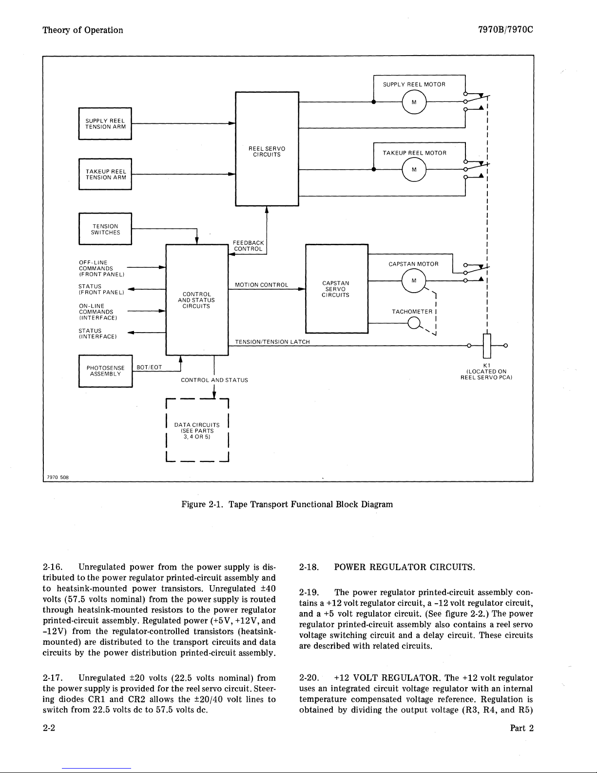
and front panel indicators are also provided by the control
and status circuits. Figure 2-1
of
OVERALL
the tape transport circuits.
of
the transport circuits.
FUNCTIONAL DESCRIPTION.
to
the interface. Off-line com-
and
data circuits. Status signals for the interface
is
a functional block diagram
of
the transport
to
aid in understand-
data
OF
of
mag-
circuits,
II
OPERATION
the
2-9. A Rewind command generated by
will initiate the rewind sequence. The control and status
circuits place the capstan servo circuits
verse mode and switch the reel servo feedback circuits. The
capstan rewinds tape
with current feedback. When the trailing edge
beginning-of-tape
status circuits terminate
second delay, establish a load
2-10. Pressing RESET releases the tape unit from interface control. Pressing REWIND in this condition rewinds
the tape
take-up reel, the tension arms
switches, the capstan
motors are shorted. This provides dynamic braking
reel motors.
2-11.
on
the supply reel. When the tape
CIRCUIT
at
160
ips and the reel servo operates
(BOT) tab
motor
is
detected, the control and
the
rewind mode, and after a one-
point
contact
circuit
DESCRIPTIONS.
in
search mode.
the tension arm limit
is
broken and the reel
interface
a high-speed re-
of
is
run-off
of
of
the
the
the
2-5. At initial power-on, the capstan
open, and the reel servo motors are shorted. When the LOAD
switch
are completed. When tape tension
arms swing away from the tension limit switches. With tape
tensioned, the capstan and reel
When the
circuits initiate a load
the reel servo circuit operates with voltage feedback and the
capstan servo pulls tape forward
sense assembly, the control and status circuits terminate the
load point search, and tape motion stops. The control and
status circuits provide a load
and the
control
controls have
of
data
voltage feedback and tension
of-tape tab
vide the interface with an end-of-tape (EOT) status.
is
pressed, the capstan
LOAD switch
point
2-6. When the load
front
panel LOAD indicator illuminates.
2-7. Pressing the ON-LINE switch establishes interface
of
the tape unit. Except for RESET, the front panel
no
control
releases the interface control and allows
the tape unit.
2-8. When the tape unit
is
being processed, the tape unit pulls tape
nous speed
as
required. The reel servo circuits operate with
is
detected, the control and status circuits pro-
motor
is
motor
is
released, the control and status
search. During load
at
20
point
tab
is
point
of
the tape unit. Pressing RESET
is
under interface control and
is
maintained. When the end-
motor
circuit
and reel
established, the tension
returns are maintained.
detected by the photo-
status
ips.
motor
to
the interface,
front
panel control
point
at
synchro-
circuits
search,
is
2-12. The following paragraphs describe the power supply circuits, control and status circuits, capstan servo circuits
and reel servo circuits
of
the circuits are provided
operation
schematic diagrams
2-13.
2-14. The power supply
a power transformer, three center-tapped bridge rectifiers,
filter capacitors, and bleeder resistors.
primary circuit
switch
power on-off switch, and a line filter/power connector_
When 115
of
vides overload protection. When 230 Vac power
the two primary windings
series, and fuse F2
ing
2-15. The power distribution circuits are
distribution
and connectors for power distribution. The assembly also
contains a printed-circuit connector for the power regulator
printed-circuit assembly.
cuits and the ±12 volt distribution circuits provide circuit
protection.
of
the circuits. Refer
POWER SUPPLY AND POWER DISTRIBUTION
CIRCUITS.
that
allows selection
Vac power
the power transformer are in parallel and fuse F1 pro-
to
provide overload protection.
PCA. The assembly contains secondary fuses
of
the tape transport. Block Diagrams
as
an aid in understanding the
to
section VII for detailed
of
the tape transport.
of
the tape transport consists
(See figure 7 -2.) The
of
the power supply transformer includes a
of
115
or
230 Vac operation, a
is
selected, the
of
the power transformer are
is
placed in series with the primary wind-
Silicon diodes in the ±20 volt cir-
two
primary windings
is
selected,
on
the power
of
in
Part 2
2-1
Page 5
Theory
of
Operation
SUPPL Y REEL
TENSION ARM
TAKEUP
TENSION ARM
REEL
SERVO
REEL
CIRCUITS
SUPPLY REEL MOTOR
M
TAKEUP
REEL MOTOR
M
7970B/7970C
bl
7970 508
TENSION
SWITCHES
OFF-LINE
COMMANDS
(FRONT
PANEL!
STATUS
(FRONT
PANEL!
ON-LINE
COMMANDS
(INTERFACEI
STATUS
(INTERFACEI
PHOTOSENSE
ASSEMBLY
t
CONTROL
AND
STATUS
CIRCUITS
BOT/EOT
t
CONTROL
r-~,
I
DATA
CIRCUITS I
(SEE
PARTS I
3,4
I
L
OR
__
Figure 2-1. Tape Transport Functional Block Diagram
51
I
AND
FEEDBACK
STATUS
-.J
CONTROL
MOTION
CONTROL
TENSION/TENSION
LATCH
CAPSTAN
SERVO
CIRCUITS
CAPSTAN MOTOR
M
'1
TACHOMETER I
'-.J
I
1
I
I
I
I
I
I
I
I
·1
I
1
I
I
I
I
Kl
(LOCATED
REEL SERVO
ON
PC
AI
2-16.
tributed
to
Unregulated power from the power supply
to
the power regulator printed-circuit assembly and
heatsink-mounted power transistors. Unregulated ±40
volts (57.5 volts nominal) from the power supply
through heatsink-mounted resistors to the power regulator
printed-circuit assembly. Regulated power (+5
-12V) from the regulator-controlled transistors
mounted) are distributed
to
the transport circuits and data
circuits by the power distribution printed-circuit assembly.
2-17.
the power supply
ing diodes CR1 and CR2 allows the
switch from 22.5 volts dc
Unregulated ±20 volts (22.5 volts nominal) from
is
provided for the reel servo circuit. Steer-
±20/40
to
57.5 volts dc.
2-2
is
routed
V,
+ 12V, and
(heatsink-
volt lines
is
dis-
2-18.
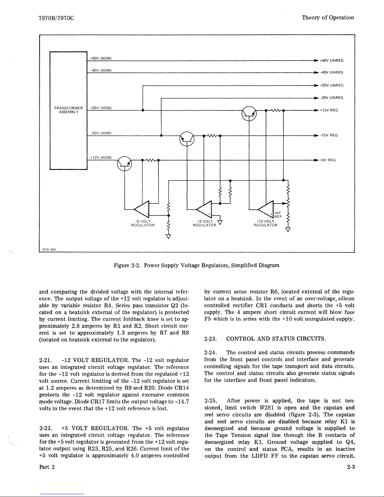
POWER REGULATOR CIRCUITS.
2-19. The power regulator printed-circuit assembly contains a +
and a +5 volt regulator circuit.
12
volt regulator circuit, a
-12
volt regulator circuit,
(See figure 2-2.) The power
regulator printed-circuit assembly also contains a reel servo
voltage switching circuit and
a delay circuit. These circuits
are described with related circuits.
2-20. +12 VOLT REGULATOR. The +12 volt regulator
uses an integrated circuit voltage regulator with an internal
to
temperature compensated voltage reference. Regulation
obtained by dividing the
output
voltage (R3,
R4,
is
and R5)
Part 2
Page 6
7970B/7970C
Theory
of
Operation
TRANSFORMER
ASSEMBLY
+40V (NOM)
-40V
(NOM)
(NOM)
+20V
-20V (NOM)
+12V (NOM)
~&
J
+5
VOLT
REGULATOR
'"'"
~:9
~
~&
/1-
+
-12 VOLT +12
REGULATOR REGULATOR
~
VOLT
REF
~
+40V UNREG
-40V UNREG
+20V UNREG
-20V UNREG
+12V
REG
-12V
REG
+5V
REG
7970·509
Figure 2-2. Power Supply Voltage Regulators, Simplified Diagram
and comparing the divided voltage with the internal refer·
ence. The
able by variable resistor R4.
cated on a heatsink external
by current limiting. The current foldback knee
output
voltage
of
the +12 volt regulator
Series pass transistor
of
the regulator)
is
adjust·
Q2
is
protected
is
set
to
(lo-
approximately 2.8 amperes by R1 and R2. Short circuit current
is
set
to
approximately 1.3 amperes by R7 and R8
(located on heatsink external
-12
2-21.
VOLT REGULATOR. The
to
the regulator).
-12
volt regulator
uses an integrated circuit voltage regulator. The reference
for the
volt source.
at
protects the
mode voltage. Diode
volts in the event that the + 12 volt reference
2-22.
-12
volt regulator
Current limiting
1.2 amperes
+5
VOLT REGULATOR. The
is
derived from the regulated + 12
of
the
-12
volt regulator
as
determined by R9 and R20. Diode CR14
-12
volt regulator against excessive common
CR17 limits the
output
+5
voltage
is
lost.
volt regulator
to
is
set
-14.7
uses an integrated circuit voltage regulator. The reference
+5
for the
lator
output
+5
volt regulator
volt regulator
using R23, R25, and R26. Current limit
is
generated from the + 12 volt regu-
is
approximately 4.0 amperes controlled
of
the
by current sense resistor R6, located external
of
lator on a heatsink. In the event
controlled rectifier
CR1 conducts and shorts the +5 volt
an over-voltage, silicon
of
the regu-
supply. The 4 ampere short circuit current will blow fuse
is
F5 which
in series with the +10 volt unregulated supply.
2-23. CONTROL AND STATUS CIRCUITS.
2-24. The control and status circuits process commands
from the front panel controls and interface and generate
controlling signals for the tape transport and data circuits.
The control and status circuits also generate status signals
for the interface and front panel indicators.
2-25. After power
sioned, limit switch
is
applied, the tape
W2S1
is
open and the capstan and
is
not
ten-
reel servo circuits are disabled (figure 2-3). The capstan
and reel servo circuits are disabled because relay
deenergized and because ground voltage is supplied
the Tape Tension signal line through
deenergized relay
on the control and status
output from
the
Kl.
Ground voltage supplied
PCA,
LDFD
FF
to
the
B contacts
results in an inactive
the capstan servo circuit.
to
K1
to
of
Q4,
is
Part 2
2-3
Page 7
Theory
of
Operation
7970B/7970C
Also, ground voltage supplied
servo
PCA
holds switch Q20
closed, grounding the input
Q2, Q4, and Q6. Ground voltage applied
reel servo amplifier
PCA, by the Tape Tension signal
and through the normally closed contacts
switch, cause it
to
close switches Q16, Q17, and Q20
on the reel servo amplifier
reel servo amplifiers grounded,
abled. Relay
K1
is
also kept deenergized through the
normally closed contacts
on
the reel servo amplifier
switch
is
pressed, +5 volts
R103 to activate the Tension signal
the reel servo amplifier
energizes relay K1.
(Once energized,
to
Q22
on
the capstan
on
the capstan servo
to
motor drive amplifiers
to
Q19
of
the LOAD
PCA.
With the inputs
the
reel motors are dis-
of
the LOAD switch and Q13
PCA.
When the LOAD
is
supplied through R9 and
to
Q13 and Q19 on
PCA.
The high input
K1
remains ener-
to
on
to
PCA
the
the
Q13
gized, through R109, CR11, and Q13, until tension
lost.) Pressing the LOAD switch also applies a high
on
input to Q19
gate Q19 holds Q16, Q17, and
inputs are high. With
the reel servo amplifier
Q20 open if either
K1
energized,
both
are high causing switches Q16, Q17, and
reel servo amplifier
ments for enabling
PCA
to
open. Thus,
the
reel servos (K1 energized and
PCA.
inputs
Q20
both
Nand
of
its
to
Q19
on
the
require-
switches Q16 and Q17 open) are met and the reel
servos tension the tape. Thus, with K1 energized and
Q20
on
the reel servo amplifier
PCA
capstan servo
capstan servo
(through Q21) opens Q20
PCA
and enables the amplifier. With tape
tension established, tension arm switch
supplying a high input
ward
FF
and
to
Q19
to
to
the reel servo amplifier
2-26. When the LOAD switch
search sequence
set. The
to
signal
output
clock the Load Forward flip-flop (U12A). The LFWD
is
gated with DELAY
is
initiated. Load Latch (U1A and U2A)
of
the load latch
PCA
open, Q22
W2S1
terminal D
to
provide the capstan servo
of
the Load For-
is
released, the load point
is
gated with
REW
on
on
closes,
PCA.
(false)
the
the
with the load point search command.
to
the interface and rewind status
to
assembly
illuminate the REWIND indicator.
2-30. When the trailing edge
of
the load
to
the
tected during rewind the Load Point flip-flop
is
Rewind flip-flop
11). Load point also gates U3B
set through the rewind clock input (U6B-
to
prevent rewind commands
from clearing the Rewind flip-flop. With the Rewind
flop set, the Load Forward flip-flop
This starts the load
point
search mode.
is
set through gate U13A.
2-31. The control and status printed-circuit assembly
tains a unit select network
that
allows up
to
controlled by one interface. The network consists
(W1)
is
jumper
position
the interface.
and 5 connecting pins (OFF, 0,
of
the jumper determines the unit
If
the units connected
to
to
the interface are
equipped with the unit select switch option, the jumper
must be in the
position the select match circuitry
printed-circuit assembly
OFF position. With the jumper in the
of
the control and status
is
disabled.
If
the tape units are
equipped with the unit select switch option, the jumper
must be connected
to
positions 0 through 3 depending upon
unit designation.
2-32. The unit select command from
(CSO,
CS1, CS2 or CS3)
is
gated with ON-LINE
generate SOLA and SOLB (selected and on-line). The
SOLA condition allows status signals
the interface. The SOLB condition
to
is
gated with
(load sequence completed) to generate EXT (external
control). The EXT condition allows interface commands
to
is
be processed. The OFF-LINE command from the
not
interface does
LINE command
to
clear the On-Line latch (U1D and U2B).
require the EXT condition. The OFF-
is
gated with the unit select command
control switch
point
tab
is
de-
is
set and the
flip-
con-
four units
to
of
1,
2,
3)_
The
be selected by
OFF
not
the
interface
be
supplied
COMP
be
a
to
to
2-27. The DELAY signal
is
generated by a delay circuit
located on the power regulator printed-circuit assembly. The
delay circuit provides a one-second delay when changing
to
from a high speed operation
a synchronous
search mode.
is
2-28. When the load point tab
is
Load Forward flip-flop
cleared by
detected (BOT), the
LP
U13B. Pressing RESET will also clear the Load Forward
flip-flop.
search motion
Load Complete flip-flop
When
will
Load Forward
is
cleared, tape load point
stop. The edge transition
U12B. Except for a rewind condition, Load Complete remains set during normal operation
of
the tape transport.
2-29. Rewind flip-flop
REWIND switch when the unit
face command
Rewind flip-flop
(U4B and U3A)
REW
is
is
U6B
is
cleared
is
off-line,
when the unit
is
cleared, the Rewind Status flip-flop
set. This provides rewind status
2-4
or
load point
through U16D and
of
LDFD clocks
by
pressing the
or
by inter-
on-line. When the
SRW
2-33. The Rewind command (REW) from the interface
gated with EXT
provided
and high-speed (FWD, REV and
to
provide motion commands
that
to
clear (assert) the Rewind flip-flop (U6B),
tape
is
not
at
load
point. The forward, reverse,
HIGH SPEED) are gated
to
the tape transport servos
and data circuits.
All
2-34.
status signals
SOLA. The load point status (SLP) indicates
is
at
unit
load point (load point tab under photosense head).
The end-of-tape status (SET) indicates
to
the interface are gated with
that
the tape
that
the tape
is
at
beyond the end-of-tape tab. The rewind status (SRW) indi-
cates that the tape
point search operation. The ready status (SR) indicates
the tape unit
is
complete
is
(not
mode). The on-line status (SL) and file protect status
indicate
that
stalled on the supply reel hub
is
rewinding
or
in an automatic load
selected, on-line, and that the load sequence
rewinding and
not
in a load point search
(SFP)
the. unit
is
on-line, and that the tape reel
is
not
equipped with a write
that
enable ring.
Part 2
is
or
in-
Page 8
Page 9
7970B/7970C
Theory
of
Operation
2,35.
The one-second delay (generated on the power
regulator printed-circuit assembly) following a high-speed
reverse command prevents additional high speed commands
from being processed by the control and status circuits. The
delay also prevents the load point search from occurring for
one-second following a rewind operation.
2-36.
CAPSTAN SERVO CIRCUITS.
2-37. The capstan servo circuits control the speed and
direction
The capstan servo consists
and a capstan servo printed-circuit assembly. The servo
of
tape motion across the magnetic head assembly.
of
a capstan motor/tachometer
cir-
cuit employs current and velocity feedback. The velocity
is
feedback
ometer attached to the capstan
back
is
motor
provided by the magnetic moving coil tach-
motor
shaft. Current feed-
provided by a pair
return circuit. Figure
of
sensing resistors in the capstan
2-4
is
a block diagram
of
the
capstan servo circuit.
2-38. Motion commands from the control and status
printed-circuit assembly control switching circuits and a
polar ramp generator. The
output
of
the ramp generator
bi-
and high-speed control signals control the capstan closedloop servo amplifier. The capstan servo amplifier consists
of
an integrated circuit servo preamplifier (U4) and a capstan
power amplifier
(Ql
through Q6).
2-39. The forward and reverse switching circuits contain
temperature compensated zener diodes
that
provide a basic
reference voltage for forward and reverse speeds. When a
FWD
command from the control and status circuits
service switch
verse biased. Bias current for CR6
R33
to
(U2 and U3). A REV command
switch
in
S2
is
placed in the on position (up),
is
then provided through
establish a
the
-6.2
volt reference for the ramp generator
or
placing the REV service
on position (up) will provide bias current for
of
Q7
FWD
is
re-
CR2 through R27. CR2 will provide a +6.2 volt reference
for the ramp generator. The forward and reverse reference
voltages
to
at
the
output
control the forward
of
U3
are independently adjustable
or
reverse speeds.
HSFWD------~----------------~_:~::~
LPSEARCH-----------------+~----~
TENSION
----------------4~
7970511A
'-
....
--------------------------------------------------------------_
HSFWD
L---o-~
.12V
12V
OFFSET
TENSION
TO
REE L
cCA
SE
RVO
Part 2
Figure 2-4. Capstan Servo, Block Diagram
2-7
Page 10
Theory
2-40.
of
Operation
The bi-polar ramp generator consists
grated circuit operational amplifiers
cal 8-volt clipping network
ramp control network
(CR7 through CR11), and a
(R42/C28).
of
two inte-
(U2 and U3), a symetri-
is
10
volts
per
volt determined by RIO and R11. The power
amplifier
is
operated in class B with Q6 providing negative
current for forward motion and
rent
for reverse motion.
7970B/7970C
Q5
providing positive cur-
2-41. Operational amplifier
saturating
is
given
down
comparator
or
removed. Near the end
U2
changes from a saturating comparator
when a forward
amplifier with the non-inverting input
2-42. The
clipping network
output
of
U2
(CR7 through CR11) which establishes
current for the ramp control network. The slope
ramp
is
determined by the current through R42 (RAMP
is
U2
initially operates
of
at
held
to
8 volts by a symetrical
or
reverse command
a ramp-up
or
to
a linear
O-volts.
as
ramp-
of
the
control) into integrating capacitor C28. Feedback through
R66 nulls the reference input voltage
voltage
of
the ramp generator (U3-6)
ratio determined by R66 (R35 + R34)
2-43. When the Forward or Reverse command
the current through R66 drives operational amplifier
to
saturation and the ramp integrates the 0 volts.
output
of
the ramp generator (U3-6) approaches 0 volts,
reverts
generator
to
a linear amplifier and the
is
maintained
at
0 volts.
to
U2
and the
is
held steady by the
or
R66 (R29 + R28).
output
is
removed,
As
output
of
the ramp
U2
in-
the
U2
2-44. A High-Speed Forward command (HSFWD) from
the control and status circuits or placing the +
switch in the on position (up) will allow
conduct
is
of
and reverse bias Q8. With Q8 reverse biased, C25
charged through R49. The exponential voltage at the base
Q9 rises
to
+ 12 volts
but
is clipped at +6 volts when Q9
CR12 and CR13
saturates. When the HSFWD command
+160 service switch
is
placed in the
off
U1B conducts placing U1B-4, CR12, and CR13
This allows Q8
to
conduct and C25 discharges through R48.
The threshold caused by the base emitter turn-on voltage
Q9
and the diode drop across CR14 results in a delay
approximately 100 ms before motion starts
2-45. A High-Speed Reverse command (HSREV)
ing the
-160
service switch
the high-speed reverse ramp circuit
in
the
on
position, (up) will cause
to
function the same
the high-speed forward ramp circuit, except
polarities are reversed. Capacitor
C26
is
160 service
is
removed
or
position (down),
at
0 volts.
or
stops.
or
plac-
that
voltage
charged through
to
the
of
of
as
R56 and discharged through R54 and R55.
2-46. The
circuits does
the capstan servo
amplifier resulting in a nominal
2-47. The
LOAD command from the control and status
not
control a ramp circuit. The load switch
is
a single step input
to
the capstan servo
of
20 ips tape motion.
outputs
of
the bi-polar ramp generator, highspeed forward ramp generator, high-speed reverse ramp generator and load switch form a summing junction at the input
of
the capstan servo preamplifier (U4). Diodes CR17 and
CR18 provide clipping
load. The preamplifier drives the capstan
plifier (Q1 through Q6). The dc gain
to
protect
the amplifier from over-
motor
power am-
of
the power amplifier
a
2-48. A
the tachometer
sponse
notch
filter in the velocity feedback circuit from
is
selected
of
the motor-tachometer combination. A compensat-
to
attenuate
the mechanical re-
ing network in the current feedback circuit
depending upon synchronous speed
of
the tape unit.
2-49. Transistor switch Q22 senses the presence
tape tension. While the tape is tensioned, Q22 is on,
keeping switch
Q22 turns off, allowing
input
of
Q20 off. However, when tension is lost
Q20
to
turn
on
motor
drive amplifiers Q2, Q4, and Q6
ground. This disables the capstan servo. The capstan
motor
relay
energized. Relay
button
circuit
K1
is
completed through
on
the reel servo amplifier
K1
is energized when the LOAD push-
is pressed. Once energized,
the
PCA
it
remains energized
until tension is removed.
2-50. REEL SERVO CIRCUITS.
2-51. The reel servo circuits consist
of
a tension circuit,
a voltage switching circuit, a delay circuit, voltage/current
feedback switches, tension arm photosense circuits, preamplifiers,
is
motor
power amplifiers, and reel motors. Figure 2-5
a block diagram
of
the reel servo circuit.
2-52. At initial power-on, the tension circuit
The normally closed contacts
prevent Q13
the
LOAD control allows Q13
K1. With
of
the tension circuit from conducting. Pressing
K1
energized, the capstan and reel servo
circuits are completed.
As
of
tape
LOAD
to
is
pushbutton
conduct, energizing relay
tensioned and the tension
arms swing away from the limit switches, power through the
limit switches maintain a forward bias
is
removed,
across the reel
or
tape tension
motor
is
windings
lost, the relay contacts short
to
2-53. The voltage switching circuit
of
Q13. When power
provide dynamic breaking.
is
power regulator printed-circuit assembly. During a highspeed operation forward or reverse, power
power amplifiers
is
switched from 22.5 volts
(nominal).
2-54. During a high-speed reverse operation (rewind), the
HSREV command from the control and status circuits
gated with TENSION. When
r/min, the
motor
voltage exceeds the break-down voltage
both
reel motors approach full
CR4. The condition established by the gating
and Tension allows current through
Q5. Voltage switch
the
+20/40
printed-circuit assembly
volts from entering the
Q6/Q7
conducts placing +57.5 volts on
line. Diode CR2
is
back-biased preventing +57.5
+20 volts line.
CR4
on
the power distribution
is
also selected
of
and switch the
to
B contacts
when
is
of
K1
is
disabled.
switch
motor
located
to
the
to
57.5 volts
on
the
motor
is
of
of
HSREV
to
forward bias
2-8
Part 2
Page 11
7970B/7970C
+SV
~~~~-4~~~~~~~~~~~AI
Theory
KIA
(ENERGIZED)
).
of
Operation
I
I
I
I
I
I
I
I
L
+20V
------------iM-----
-----------t4----i>---+---,--II
-20V
HSFWD
__
_
R26
...
---+-..
">cHI-_
-20/40V
R27
+20/40V
..
-20/40V
MOTOR VOLTAGE
DELAY
CONTROL
STATUSPCA
FEEDBACK CONTROL
TO
AND
R47
VOLTAGE
FEEDBACK
SUPPLY
REEL
MOTOR
-SV
7970-512
Part 2
VOLTAGE
>-
.... -__
-20/40V
RB
R7
-<11-
____
Figure 2-5. Reel Servo, Block Diagram
RIOS
FEEDBACK
-----------
...
I
.J..
KIC
TAKEUP
REEL
MOTOR
(ENERGIZED)
2·9
Page 12
Theory
2-55. During a high-speed forward operation, the voltage
switching circuits function the same
operation.
voltage
of
Operation
HSFWD
to
switch the
is
gated with tension
-40
volt switch
as
in the fast reverse
to
allow
(QI2/QI3).
motor
7970B/7970C
C8
is
then charged through R33 (one-second time constant).
is
When C8
feedback control changes from
switches
charged
to
0 volts.
to
+5V, Q16 and Q18
-8V
conduct
to
+8V. The DELAY
and the
2-56. The delay circuit
printed-circuit assembly. The delay circuit provides an
tional one-second delay following the end
command. The one-second delay prevents further high-speed
commands from the interface from being processed during
the one-second period. The one-second delay
switch the reel servo operating mode from voltage feedback
to
current feedback. The additional one-second following a
high speed operation allows the reel servo
current feedback mode until reels are slowed.
2-57. During normal operation, U5A-3 and U5B-4 rest
o volts. A HSFWD
and status circuits will cut-off U5A
for Q15
ducts, capacitor C8 immediately discharges through Q15
causing Q16 and Q18
reel servo changes from approximately +8 volts
mately
Q17 and the DELAY line switches
2-58. When the high-speed command
HSREV)
is
supplied through R28
-8
volts. The negative potential also reverse biases
is
removed and Q15 loses base current, capacitor
is
located on the power regulator
of
a high-speed
is
also used
to
operate in a
or
HSREV command from the control
or
U5B
and base current
or
R29. When Q15 con-
to
be cut-off. Feedback control
to
approxi-
to
+5
volts.
(HSFWD
addi-
to
to
at
the
or
2-59. The reel servo tension arm assemblies contain dual
that
element photo-conductors
shining through a slotted disc. The slot
spiral attached
slot exposes different areas
result, the
to
the position
2-60. The reel servo preamplifier
tional amplifier
sion arm. The tension arm photo-conductor
ended, therefore, an off-set
The preamplifier drives a class B
The
motor
2-61. When operating in a normal mode (synchronous
or
load speed), the servo operates with voltage feedback.
The +8 volts from the feedback switching network
back control) back-biases the feedback FET switch (Q14
and
QI5).
RI05.
During a high-speed operation, the feedback control
changes
biased and feedback
to
the tension arm.
output
to
of
the photo-conductor
of
the tension arm.
that
amplifies the position
power amplifier has a gain
Feedback
-8
is
volts. The feedback FET switch
is
current through the switch.
are illuminated by a lamp
is
in
the
form
of
As
the arm moves, the
of
the photo-conductor.
is
proportional
is
an integrated opera-
error
output
is
provided by R39
motor
then provided through R47 and
drive amplifier.
of
10 volts
of
the ten-
is
or
per
is
forward
As
single-
R41.
volt.
(feed-
a
a
2-10
Part 2
Page 13
7970B/7970C
Performance Checkout
SECTION
PERFORMANCE
3-1.
3-2. This section provides checkout instructions
ify
specifications. The test procedure assumes
ing general conditions apply
structions
3-3. TEST EQUIPMENT REQUI RED.
3-4. For the purpose
that
computer
the
ing instructions for the equipment
tation applicable
3-5.
available
all adjustments. Computer operation
following electronic test instruments (or equivalent) are
also required:
Generator.
meter Plug-In.
3·6.
port
various signals for accurate speed measurements
3-7. CHECKOUT PROCEDURES.
3-8. Performance checkout procedures for the tape unit
consist of:
I NTRODUCTI ON.
that
the tape unit conforms
to
the contrary are stated as part
the person conducting
or
an off-line test set
following requirements.
to
the
equipment.
a.
Provides all standard functional commands.
b. Responds
An
as
a.
HP
HP
b.
c.
HP
In addition
test tape
a.
Preliminary Power-Off Checks.
Operator Control Checks.
b.
to
all status outputs.
HP
13191A Control and Status Test Board
a service accessory and will meet the needs for
140A Oscilloscope with
1421A Dual-Trace Preamplifier (for
5245L Counter with
to
the listed test equipment, a trans-
HP
part number 5080-4525
to
published performance
at
all times unless specific
of
this procedure,
the
test will be using either a
that
is
It
is
also presumed
is
provided by documen-
is
HP
HP
5265A Digital Volt-
to
that
the follow-
of
a test routine.
it
is
presumed
capable
of
meeting
that
operat-
also suitable. The
1421A
that
Time
HP
140A).
generates
is
required.
Base
ver-
in-
III
CHECKOUT
c.
Service Switches and Accessory Checks.
d. Tape
e.
f.
g.
3-9.
3-10. Preliminary power-off checks are performed
follows:
a.
and have no end play.
b.
should operate freely and should have clearance between
of
face
ness without binding).
is
c. Tension Arm Limit Switches: The three limit
switches associated with the tension arms must operate
when the arm
stop. The roller on the switch arm should be approximately
on the center
stop. There should be positive travel
yond
the
check can
or
with an ohmmeter if room noise
d.
finger nominal location dimensions should be
Path Evaluation.
Power Supply Voltage Checks.
Tape Speed and Capstan Servo Checks.
Transport Function, Motion, and Status Checks.
PRELIMINARY POWER-OFF CHECKS.
Tape Rollers: The tape rollers must operate freely
Head Crosstalk Shield: The head crosstalk shield
head and shield (room
is
approximately 1/8 inch from the rubber
of
the arm when the arm
point
at
which it actuates the microswitch. The
be
made audibly if ambient noise level permits,
Write Enable Sensing: The write enable sensing
(1) The distance between the outside surface
the write enable sensing finger and the outside flange diameter
should be 3/32-inch (nominal).
(2) In the file protected position (inoperative),
the dimension between the
sensing finger and the
turntable should be 3/16-inch (nominal)
above the turntable surface.
(3) In the write enable position (with solenoid
energized) the
should be 1/16-inch below the turntable surface.
(4) The sensing finger must
table under any condition.
to
slip a punched card thick-
is
fully against
of
the switch lever be-
is
too
high.
as
of
the reel turntable
outer
outer
face
of
outer
tip
of
the sensing finger
not
touch the turn-
follows:
tip
of
the reel
the
as
of
the
Part 2
3-1
Page 14
Performance Checkout
7970B/7970C
e. Reel Retaining Knob: With the locking lever
re-
leased, the reel should slip over the rubber grip ring easily,
and it should be possible
lever
is
closed, positive resistance should be felt
ber
is
compressed. In the locked position,
possible
place a piece
the
should
hours
to
move the reel by hand.
of
masking tape
hUb.
A mark placed in alignment on
not
become misaligned by more
of
operation. To correct tape reel slippage, release
locking lever and loosen the pozidrive screw,
retainer
knob
clockwise, and tighten the screw. Repeat until
tape reel mounts firmly and does
3-11.
OPERATOR CONTROL CHECKS.
3-12. Verify position
connect unit
to
appropriate power source and check the
to
easily rotate the reel. When the
as
the rub-
it
should
If
of
115/230
slippage
on
the reel, and another on
not
slip.
volt selector switch;
both
than
is
suspected,
pieces
of
1/8 inch in
rotate
the reel
not
be
tape
16
following operating modes.
3-13.
reel
the power switch on. After threading tape, press
verify
TAPE LOADING AND WRITE ENABLE. Place a
of
tape (with write enable ring) on unit and thread with
LOAD and
that
the following takes place.
a.
Tape tension
is
established. RESET indicator
il-
luminates.
the load command and will return the tape to the
position (LOAD indicator
may be terminated prior
Transfer
to
on-line
on
with tape stopped). Rewind
to
load
point
by pressing RESET.
is
also possible immediately following
load
point
this sequence.
3-17. SERVICE SWITCHES AND
ACCESSORY
CHECKS.
in
3-18. There are three service switches incorporated
the
capstan servo card. These together with the REWIND and
LOAD controls provide a means
modes for service and
lor adjustment purposes. There
of
operating all five drive
is
no
capability for cyclic drive operation.
HP
3-19. The
13191A
available for use with the tape unit. With this test board
is
possible
of
the control and status function
to
completely adjust and verify the performance
Control and Status
of
a tape unit
Test
Board
under
is
it
offline conditions. Complete operating details are included with
the test board. The
Board provides normal drive modes
gramming which
HP 13191A Control and Status Test
as
well
as
cyclic pro-
is
suitable for adjustment
of
the capstan
start/stop ramp. The board also includes status indicator
lamps
to
verify all normal status functions. The test board
is
installed in the connector
status
PCA.
of
the tape unit control and
b.
WRITE ENABLE indicator illuminates.
20 ips
to
load
point
c. Tape moves forward at
tab
(BOT tab).
d.
LOAD indicator illuminates.
3-14.
control and status
OFF
and load tape. Following completion
with tape positioned
press
commands.
process will also result in
pleting the search (LOAD indicator
the unit will
tion
3-15. DYNAMIC BRAKING AND
POWER
well
turn
stop
ON-LINE TRANSFER AND RESET. Place the
PC
assembly unit select jumper
pin (this
ON-LINE and verify
is
not
the same
at
as
OFF
on unit select option)
of
a load sequence
load point (LOAD indicator on),
that
unit will respond
to
Pressing ON-LINE while load point search
ON-LINE operation upon com-
is
ON). While ON-LINE,
not
of
RESET.
respond
to
local controls with the excep-
RECOVERY FROM
FAILURE. Place unit in rewind mode after tape
into
take-up reel. When full rewind speed
power switch
without
off
to
any damage
simulate power failure. Tape should
to
tape. Proceed with recovery
is
in
the
external
is
in
reached,
to
on-line status by following normal load sequence. Except
that
when tape unit goes into the load
load
point
tab may be simulated by pressing the RESET
button.
3-16. REWIND
This can then be followed by an on-line command.
OPERATION. The REWIND control
operational only while the unit
point
search mode,
is
in the reset state which
permits local control. The rewind command will override
3-20. TAPE PATH
3-21. With undamaged tape threaded
EVALUATION.
on
and with the unit in the appropriate operating mode,
ate the following characteristics
a.
Capstan Height: Capstan height should be such
the tape
edge
is
guided equal distance in from the
of
the capstan. The air escape grooves provide a means
of
the tape path.
for judging.
b.
Tension Position: Arms should be aligned with the
centering marks on the rear
ceptable provided the arm
than the diameter
of
the arm.
c. Tape Tracking
of
the casting. Position
is
not
out
of
location by more
Over the Tape Guides: Tracking
over the guides should be smooth with no evidence
forces anywhere in the tape path. Transverse reflected light
may be used
is
the 1/2-inch width
points
d.
sembly should be parallel
tioned
3-22.
to
assist in judging. Light reflections across
of
the tape should
of
stress.
Photosense Position: Face
to
the path
1/8
inch from the tape.
not
of
photosense head
of
the tape and posi-
POWER SUPPLY VOLTAGE CHECKS.
is
3-23. Both regulated and unregulated supplies should be
checked for the following specifications.
the
outer
be
bent
tape unit
evalu-
that
and inner
is
ac-
of
edge
due
to
as-
3-2
Part 2
Page 15
7970B/7970C
3-24. REGULATED SUPPLY VOLTAGES. Regulated
voltages will remain within tolerances over a primary voltage
of
range
as
±10 percent.
specified below. The peak-to-peak ripple values are nom-
inal and minor variances may be expected. Ripple
DC
voltages and tolerances are
is
stated
to
be
under tension-only conditions.
+5
a. The
volt supply must be +5.000 ± 0.050 Vdc.
b. The ±12 volt supplies must be 12.000 ± 0.360 Vdc.
3-25. UNREGULATED SUPPLY VOLTAGES. Unregu-
lated supply voltages are a direct function
The following table
only at a line voltage
nominal and apply at
a.
±40 Vdc: Nominal value
150 mv
POp
(sawtooth).
of
nominal values should be judged
of
115 volts.
60
Hz.
is
of
line voltage.
RMS
ripple values are
±57.5 volts; ripple
of
Performance Checkout
that
the
output
of
For
the follow-
the read
HP
part
bit-to-bit distances be read, and
preamplifier be connected
number
accurately spaced
50S0-4525 Transport Test Tape provides frequencies
to
better
to
than
a suitable counter.
0.1 percent.
ing tests reference frequencies are based on using the signal
that
will
be avail abel from the channel 3 preamplifier
track units and channel 6 preamplifier
This has a bit-to-bit spacing
duce a frequency
of
speed
30.000 ips. Frequencies for
direct ratio
of
10,000
to
the change in speed relation to 30 ips. Ex-
of
Hz
of
0.00150 inch
when reproduced at a tape
other
ample: 60 ips would produce 20,000 Hz.
seven-track units.
Use
of
nine-
and
will pro-
speeds are in
this principle
and check the following:
a. High-Speed Forward:
53,333
Hz.
160
ips, basic frequency
(1) Maximum acceptable operating limit: ±1050
Hz
(±2 percent).
(2) Adjustment recommended if greater than:
±SOO
Hz
(±1.5 percent).
is
+20 Vdc: Nominal value
b.
600
mv
Pop
(sawtooth).
c.
-20
Vdc: Nominal values
300 mv
900 mv
3-26. TAPE SPEED
Pop
(sawtooth).
+10 Vdc: Nominal value
d.
POp
(sawtooth).
AND
3-27. The tape speed and capstan servo checks consist
measuring capstan
motor
offset current, measuring long term
speed variation (tape units capable
is
+22.5 volts; ripple
is
-22.5 volts; ripple
is
+12 volts; ripple of
of
CAPSTAN SERVO CHECKS.
of
of
reading data), measur-
of
ing start and stop time and distance, measuring instantaneous
speed variations, and measuring fast forward, reverse, start
is
and stop. Included
a dynamic tape skew check for tape
units equipped with read and write electronic circuits.
3-2S. CAPSTAN MOTOR OFFSET CURRENT. Connect
or
a suitable dc voltmeter
percent resistor (R21
tors
is
sion
connected
but
no tape motion, the voltage should
to
following referenced
a.
Maximum acceptable operating limit: ±100 mv
oscilloscope across the 3 ohm 1
or
R22). The return side
pin 2
of
CJ-1. With the tape under ten-
not
to
0 V dc.
of
the resis-
exceed the
dc
at 25°C.
b. Adjustment recommended if greater than:
±SO
mv
dc.
3-29.
tape speed accuracy over any interval greater than one
ond and under each
of
LONG TERM SPEED VARIATION. Measure the
of
the
five
drive speeds. The principle
measurement requires
that
a tape having highly accurate
sec-
b. Rewind (High-Speed Reverse): Checked identically
to
the limits applicable
the rewind mode
is
to
high-speed forward, except
used.
that
c. Forward and Reverse Drive: Frequency depends
other
on tape speed and must be calculated for speeds
than
25 ips and 37.5 ips which are tabulated below. Maximum
is
acceptable operating limit
justment recommended if speed error
based on ±1 percent with ad-
is
+O.S
percent
or
greater.
is
(1) The 25 ips drive nominal frequency
Hz.
Acceptable limits are ±S3 Hz; adjustment
is
required if greater than ±65 Hz.
(2) The 37.5 ips drive nominal frequency
S,333
is
12,500 Hz. Acceptable limits are ±125 Hz;
adjustment
is
recommended if greater than
±100 Hz.
d. Load Point Search:
6,667
Hz.
(1) Maximum acceptable limit
20 ips; basic frequency
is
±1330
Hz
(±20
is
percent).
(2) No adjustment
3-30.
START
MEASUREMENT. Start measurements
(both forward and reverse) are made
ment of the characteristics defined requires
unit be driven with commands
greater than the specified start/stop times and
is
provided.
that
are adjustable
as
follows. Measure-
that
the tape
to
that
there be
periods
a provision to synchronize an oscilloscope sweep directly
to
from these commands (both start and stop). The tape
be
read may be any previously recorded tape, preferably at
SOO
cpi,
as
this provides the best resolution where measure-
ments from preamplifier
outputs
are required. Wavelength
Part 2
3-3
Page 16

Performance Checkout
7970B/7970C
accuracy
is
not
a factor in this test. Do
not
make measure-
ments during read-after write operation.
Note
The definitions apply for both forward and
reverse directions. The capstan tachometer voltage
will reverse polarity when direction
is
changed;
however, there will be no observable difference
in the preamplifier
a.
Start-Ramp Delay Time: The time (following a start
command) required for the capstan tachometer voltage
reach a value
cent
of
tion
is
b.
that
the value reached at normal drive speed. Specifica-
0.5 ± 0.5 ms.
Start-Ramp 100 Percent Time: The time (following a start command) required for the analog
preamplifier track
output
is
greater than a Vdc
to
first reach
waveforms.
100
but
percent
less than 3 per-
output
of
any
of
the peak-to-
to
peak (or O-to-peak) value established while reading an all
"1
's"
tape under steady state drive conditions. This
function
of
tape speed; the following limits apply with the
is
capstan ramp adjustment being made during the forward
start mode only.
(1) The 25 ips start-ramp
should be 14.5 ±
100 percent time
0.2 ms for forward ramp,
±0.3 ms for reverse ramp.
(2) The 37.5 ips start-ramp
should be 9.5 ±
0.2
100 percent time
ms
for forward ramp,
±0.3 ms for reverse ramp.
b. Start Balance Time: This
tween the start-ramp
100
is
the time difference be-
percent time and
start time for the tape speed involved. This period
is
allowed
the time delay
to
provide a balance in tape distance
at
full drive speed represented by the stop-
ramp delay time.
c.
One-half
of
the start-ramp time plus
ance time (both in milliseconds) multiplied by
in
inches per second equals the start distance (in inches x
3
10-
).
Specifications 0.187 ± 0.020 inch.
3-32.
forward and reverse) are made
command) required for the analog
fier
than
established
ing in all
a
STOP MEASUREMENT. Stop measurements
as
follows:
a.
Stop-Ramp Delay Time: The time (following a
output
of
to
fall
to
a peak-to-peak (or O-to-peak) value
100
percent
"l's"
b. Stop-Ramp
but
greater than 97 percent
under
steady-state drive conditions while read-
tape. Specification
is
0.5 ± 0.5 ms.
100 Percent Time: The time (following a stop command) required for the capstan tachometer
voltage
speed value and
speed and must
to
reach a level between 3 percent
a Vdc. Specification
not
exceed a time
is
a function
that
of
is
less than the specified stop time for the tape speed involved.
3-33.
STOP DISTANCE. Stop distance
is
follows:
a.
Determine stop-ramp delay time.
the
specified
of
as
it offsets
the
start
the
tape speed
(both
any preampli-
that
is
of
the value
normal drive
of
at
least 0.2 ms
calculated
time
bal-
stop
less
tape
as
3-31.
as
quires
adjustable
times and
START DISTANCE. Start distance
follows. Measurement
that
the tape unit be driven with commands
to
periods greater than the specified start/stop
that
there be a provision to synchronize an oscil-
of
the characteristics defined re-
is
calculated
that
are
loscope directly from these commands (both start and stop).
The tape
preferably
where measurements fram preamplifier
Wavelength accuracy
to
be read may be any previously recorded tape,
at
800 cpi
as
this provides the best resolution
outputs
is
not
a factor in this test. Do
are required.
not
make measurements during the read-after-write operation.
Note
The definitions apply for
both
forward and reverse directions. The capstan tachometer voltage
will reverse polarity when direction
is
changed;
however, there will be no observable difference
in the preamplifier
a.
Start-Ramp Time: This
celerate the tape from zero ips
output
waveforms.
is
the time required
to
the drive speed.
It
to
is
ac-
determined by subtracting the start delay time (measured)
from the start-ramp
100 percent time (also measured).
3-4
b. Determine Stop-Ramp Time: This
quired
speed.
to
decelerate the tape
It
is
determined by subtracting the stop-ramp delay
to
time (measured) from the stop-ramp
zero ips from the drive
100 percent time (also
is
the time re-
measured).
c. The stop-ramp delay time plus one-half the
ramp time
speed in inches
inches x
3-34.
taneous speed variation
departure
speed. Measurement
wind
of
tape.
fier
output,
(both
in milliseconds) multiplied by the tape
per
second equals the stop distance (in
Specification
is
0.187 ±0.020 inch.
10-
3
).
INSTANTANEOUS SPEED VARIATION. Instan-
is
a measurement
of
the tape velocity from its long
is
made
a.
Write a length
as
reqUired
of
to
be in position
all
b. Connect oscilloscope
position so
that
as
follows:
"l's"
to
to
any convenient preampli-
waveform
of
the short
term
tape
at
800 cpi and
reproduce this section
is
centered
and adjust main sweep sync for positive slope and
at
the zero crossover.
average
on
screen,
to
stop
term
re-
trigger
Part 2
Page 17
7970B/7970C
c.
Use
the delayed sweep feature
to
position the de-
layed sweep at the next zero axis crossover (this corresponds
to
one bit-to-bit distance) with the delayed sweep
auto
trig-
gered from a main (delaying) sweep.
d. Adjust delayed sweep rate
tion
of
the
time shift band
at
to
permit good resolu-
the zero axis crossover. During
this evaluation the vertical gain and the delaying sweep time
may be adjusted
point
is
being observed, it will be the waveform
ing from
top
left
optimize the resolution.
of
screen to
bottom
If
the correct
that
is
com-
right with the slope
to
depending on the gain and delayed sweep speed.
e. Observe the jitter band under conditions in step
"d"
in microseconds peak-to-peak time displacement and
to
multiply by tape speed
inches. This value must
which are based
(1)
on
±3 percent instantaneous speed variation:
800 cpi must
determine this distance in micro-
not
exceed the following limits
not
exceed ±37.5 micro inches
(75 microinches peak-to-peak).
not
(2) 556 cpi must
exceed ±54 microinches
(108 microinches peak-to-peak).
as
high
Checkout
as
pos-
Performance
peak-to-peak. Again gains must be adjusted
sible (both the same) and the delayed sweep trigger set for
maximum stability
of
the stable waveform. There will be a
considerable dead zone in the delaying sweep adjustment.
Use
the first operating position
from minimum delay position. There
the time differential between the stable and unstable
forms. This does
is
a function
not
represent static skew. The difference
of
oscilloscope gain and position settings.
e. Measure the peak-to-peak time band
waveform
as
it crosses the zero axis. Convert this
as
the sweep
is
moved
is
no significance to
of
the unstable
to
micro-
out
wave-
inches peak-to-peak for the tape speed involved. Worst case
must
not
exceed ±50 microinches (100 micro inches peak-
to-peak) and applies
3-36. FAST
to
forward
or
reverse mode.
FORWARD/REVERSE
START/STOP
CHARACTERISTIC. Fast forward and fast reverse characteristics are measured by synchronizing an oscilloscope with
the appropriate drive command, and observing the dc
put
of
the tachometer using the TACH test
point
out-
on the
capstan servo printed-circuit assembly.
(3)
200 cpi must
not
exceed ±150 microinches
(300 microinches peak-to-peak).
Note
The above values apply
to
both
the forward and
reverse modes.
3-35. DYNAMIC TAPE
that
variation in tape velocity which generates a differential
SKEW.
Dynamic tape skew
time position between the two outermost tracks on the tape.
Measurement
a.
to
reproduce this section
b.
plifier
Use
chopped mode (triggered by channel
sweep synchronized for positive slope triggered
is
made
as
follows:
Write a length
Use
dual-trace oscilloscope and connect
output
of
of
all
"l's"
of
tape.
the
two outside tracks (channels 4 and 5).
tape. Rewind
A)
with the main
as
required
to
at
zero axis
pream-
crossover. (Use negative slope in reverse direction.)
c. Adjust
impose
the
varying degrees
acteristics
d.
Use
(one bit-to-bit distance later) zero axis crossover
layed sweep. The delayed sweep must be
triggered on the negative slope. (Use positive slope in
verse direction.) The earliest
delayed sweep and the
jitter
that
both
channel gains and positions
to
super-
two waveforms (amplitude only; there will be
of
time difference due
to
static skew char-
).
the delayed sweep feature
of
the two tracks will sync the
other
will arrive later and will have
to
present the next
on
on
internal sync,
the de-
represents the time differential in microseconds
reo
CAUTION
Do
not
issue sequential fast drive commands
without allowing time to reach full speed
return to zero speed. Failure
caution may cause excessive power dissipation
in the reel servo amplifier circuitry. Minimum
time between commands should be 1 second
the sum
is
greater).
of
the start and stop times (whichever
is
3-37. Fast forward/reverse start
ured by observing the time (following a start
mand) required for the tachometer
its maximum value (for start time)
stop time). Nominal times are from 400
Typically,
the
value will be 600 milliseconds.
3-38. Fast forward/reverse start
termined by the time required for the ramp
to
one state
seconds. One-half
the other. This time
of
this time multiplied by
the nominal start/stop distance
3-39.
TRANSPORT FUNCTION, MOTION, AND
STATUS CHECKS.
3-40.
The following checks cover the
status and motion command connector.
to
off-line test equipment
verify proper performance
dicated.
3-41.
trol and status
to
FUNCTION COMMANDS. Select,
PC
assembly includes a jumper
establish
unit
identification where the front panel select
to
observe this pre-
or
stop times are meas-
output
or
to
fall
to
700 milliseconds.
or
stop distances are de-
is
nominally 500 milli-
of
40
inches.
1/0
Use
or
to
or
or
stop com-
to
either reach
to
zero (for
to
move from
160
ips equals
lines in the
appropriate
CS:
The con-
that
can serve
as
in-
Part 2
3-5
Page 18
Performance Checkout
7970Bj7970C
option
jumper can be placed in the
response
with load sequence completed,
the following conditions
to
responding
is
not
present.
to
controller commands, when unit
a.
Unit responds
OFF.
b. Unit responds
CSO
If
no select function
to
to
commands with jumper connected
to
0 through 3 positions when cor-
through CS3
is
desired, the
off
position which will permit
is
in on-line
and
is
not
rewinding. Verify
check the select (CS) line:
is
selected by the controlling
device.
c. When front panel select option
internal jumper in the
to
push buttons 0 through 3
When the front panel
not
respond
to
3-42. Verify
off
position and verify
is
same
OFF pushbutton
any commands from the controlling device.
that
the off-line (CL) line clears the write
condition and returns the selected tape unit
is
included, place
that
response
as
in step
is
"b"
pressed, unit must
to
the reset
above.
condition.
3-43.
MOTION COMMANDS. Verify
that
the following
external commands will place the selected and on-line tape
unit in the corresponding drive mode:
a.
Forward (CF): Tape drives forward.
b. Reverse (CR): Tape drives reverse
then
stops
at
load point tab.
CAUTION
Do
not
issue sequential fast drive commands
without
return
allowing time
to
zero speed. Failure
to
reach full speed
to
observe this pre-
or
to
caution may cause excessive power dissipation
in the reel servo amplifier circuitry. Minimum
time between commands should be 1 second or
the sum
is
3-44.
status
outputs
ready tape unit
a.
of
the start and
stop
times (whichever
greater).
STATUS OUTPUTS. Verify
that
the following
are true (low assertion) when a selected and
is
in the condition indicated.
On-Line (SL): True when selected tape unit has
been manually placed on-line.
b. Ready (SR): True when selected
tape loading cycle
is
completed, and tape unit
unit
is
is
on-line,
not
in
re-
wind mode.
c. Load Point (SLP): True when selected tape unit
has tape positioned
d.
Density (SD2, SD5,
at
the load
point
reflective strip.
or
SDS): Verify
that
selected
tape unit will display the density selected by the tape unit
density switch if this option
the tape unit will be set
is
present. Without this option,
at
SOO
cpi
but
there will be no
SDS
output.
e. Rewind (SRW): Verify
true
as
long
as
the selected unit
Must remain true until tape
that
is
is
repositioned
this status remains
in the rewind mode.
at
load point
tab.
c. Rewind (CRW): Tape unit enters rewind mode,
mains on-line.
d. High Speed (CH): Tape unit will respond only when
this
is
combined with either a forward
When so combined, tape will drive
at
or
reverse command.
160
ips speed.
CR will drive reverse past load point.
3-6
CH
re-
with
f.
File Protect (SFP): True when selected unit
is
write-enabled.
g.
End-of-Tape (EOT): True when selected unit has
moved end-of-tape tab
beyond
photosense head.
Will
main true until tab again passes photosense head in the
verse direction.
Part 2
not
rere-
Page 19
7970B/7970C Repair and Replacement
SECTION
REPAIR
4-1. INTRODUCTION.
4-2. This section provides repair and replacement procedures for the tape transport
ital Magnetic Tape Units.
4-3. REPAIR.
4-4. The etched printed-circuit assemblies (PCA's) used
are
of
the plated-through type consisting
to
both
sides
of
an insulating material. The metallic conductors are extended through the component holes by a
plating process.
of
the
PCA
mended tools and materials for use in repairing etched
The following are recommendations and precautions pertin-
to
PCA
ent
Soldering can be performed on either side
with equally good results. Table 4-1 lists recom-
repair work.
of
the
HP
7970B/7970C
of
Table 4-1. Printed-Circuit Assembly Repair Equipment
AND
Dig-
metal bonded
PCA's.
IV
REPLACEMENT
a. Avoid unnecessary component substitution; it can
result in damage
components.
b.
Do
heat may lift a conductor
Do
not
or twist drill
may damage the plated-through conductor.
c.
Use
pick
to
remove solder from component mounting holes.
d. After soldering, remove excess flux from the solder
areas and apply a protective coating
tion and corrosion.
to
the
PCA
not
use a high·power soldering iron. Excessive
or
CAUTION
use a sharp metal object such
to
remove solder. Sharp objects
a suction device (table 4-1)
circuit board and/or adjacent
damage the board.
as
an
awl
or
wooden tooth-
to
prevent contamina-
ITEM
Soldering Tool Soldering and unsoldering Wattage rating: 47-1/2
Soldering
Suction Device Removes molten solder
Resin
Solvent soldered
Solder Component
Protective Contamination and corro-
Coating sion protection corrosion-prevention properties Humiseal Protective Coating,
Tip*
(Flux)
Soldering and unsoldering Shape: pointed
from
Removes
cation
printed-circuit board repair,
and wiring connections preferred
USE
Tip
connection
excess
flux
from
area
before appli-
of
protective coating bonding agent
replacement,
Must
base
Resin
(60/40 tin/lead), 18
Good
DESCRIPTION
Temp: 8500to
not
dissolve etched
board material
(flux)
core, high
electrical
to
56-1/2W
900°F
circuit
or
conductor Aceton
tin
content
gauge
(SWG)
insulation,
RECOMMENDED MODE
Ungar
#776
Handle
Ungar
#4037
#PL111*
Ungar
Soldapullt
Arleta, California
Freon
Lacquer
Isopropyl Alcohol (100%
Krylon
Type 1 B 12 by Columbia
Technical Corp.,
New
by Edsyn Co.,
Thinner
R**
#1302
York
Heating
Woodside
with
Unit*
L
dry)
77,
*For
working on etched boards;
to
800°
F)
and Ungar #P L 113 1 /8-i nch
**
Kryton,
Inc., Norristown, Pennsylvania
Part 2
for
general purpose
ch
isel
work,
use
Ungar
#1237
Heating
ti
p.
Unit
(37.5W,
tip
temp
of
750°
4-1
Page 20
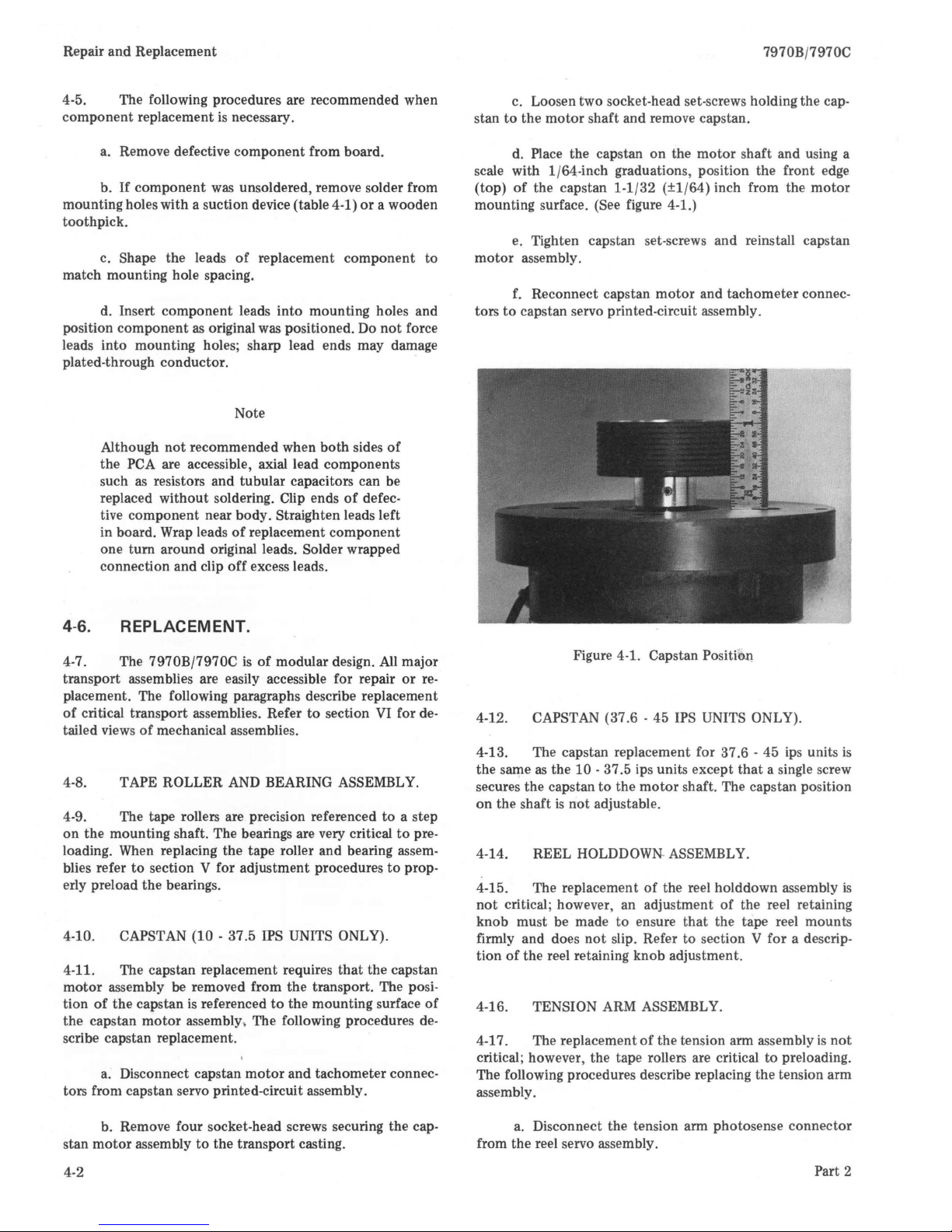
Repair and Replacement
4-5. The following procedures are recommended when
component
replacement
is
necessary.
a.
Remove defective component from board.
b.
If
component was unsoldered, remove solder from
mounting holes with a suction device (table 4-1)
or
a wooden
toothpick.
c. Shape the leads
of
replacement
component
to
match mounting hole spacing.
d. Insert component leads into mounting holes and
position
component
as
original was positioned. Do
not
force
leads into mounting holes; sharp lead ends may damage
plated-through conductor.
Note
Although
not
recommended when
both
sides
of
the PCA are accessible, axial lead components
such
as
resistors and tubular capacitors can be
replaced without soldering.
Clip ends
of
defective component near body. Straighten leads left
in board. Wrap leads
of
replacement component
one
tum
around original leads. Solder wrapped
connection and clip
off
excess leads.
4-6. REPLACEMENT.
4-7. The 7970B/7970C
is
of
modular design.
All
major
transport assemblies are easily accessible for repair
or
replacement. The following paragraphs describe replacement
of
critical transport assemblies. Refer
to
section VI for de-
tailed views
of
mechanical assemblies.
4-8. TAPE ROLLER AND BEARING ASSEMBLY.
4-9. The tape rollers are precision referenced
to
a step
on
the
mounting shaft. The bearings are very critical
to
preloading. When replacing the tape roller and bearing assemblies refer
to
section V for adjustment procedures
to
prop-
erly preload the bearings.
4-10. CAPSTAN (10 - 37.5 IPS UNITS ONLY).
4-11. The capstan replacement requires
that
the capstan
motor
assembly
be
removed from the transport. The posi-
tion
of
the
capstan
is
referenced
to
the mounting surface
of
the
capstan
motor
assembly, The following procedures de-
scribe capstan replacement.
a.
Disconnect capstan
motor
and tachometer connec-
tors from capstan servo printed-circuit assembly.
b. Remove four socket-head screws securing the
cap-
stan
motor
assembly
to
the transport casting.
4-2
7970B/7970C
c. Loosen two socket-head set-screws holding the cap-
stan
to
the
motor
shaft and remove capstan.
d. Place the capstan
on
the
motor
shaft and using a
scale with 1/64-inch graduations, position the front edge
(top)
of
the capstan 1-1/32 (±1/64) inch from the
motor
mounting surface. (See figure 4-1.)
e. Tighten capstan set-screws and reinstall capstan
motor
assembly.
f.
Reconnect capstan
motor
and tachometer connec-
tors
to
capstan servo printed-circuit assembly.
Figure 4-1. Capstan
PositiEll1
4-12. CAPSTAN (37.6 - 45 IPS UNITS ONLY).
4-13. The capstan replacement for 37.6 - 45 ips units
is
the same
as
the
10
- 37.5 ips units except
that
a single screw
secures the capstan
to
the
motor
shaft. The capstan position
on
the shaft
is
not
adjustable.
4-14. REEL
HOLDDOWN-ASSEMBLY.
4-15. The replacement
of
the reel holddown assembly
is
not
critical; however, an adjustment
of
the reel retaining
knob must be made
to
ensure
that
the tape reel mounts
firmly and does
not
slip. Refer
to
section V for a descrip-
tion
of
the reel retaining knob adjustment.
4-16. TENSION ARM ASSEMBLY.
4-17. The replacement
of
the tension arm assembly
is
not
critical; however, the tape rollers are critical to preloading.
The following procedures describe replacing the tension arm
assembly.
a. Disconnect the tension arm photosense connector
from the reel servo assembly.
Part 2
Page 21
7970B/7970C
b. Using retaining ring pliers, remove
ring holding tape roller
to
tension arm. (See figure 6·6.)
outer
retaining
b. Remove the two screws
amplifier assembly
to
Repair and Replacement
that
secure
the transport casting.
the
read pre-
c. Note
the
positions
of
the shims and washers and
remove the shims, washers, and tape roller from tension arm
shaft.
d. Remove the tension arm spring.
e.
Remove the three screws and washers
Mount
to
the
the tension arm
f.
ble in reverse order
g.
Perform adjustment procedures described in sec-
tion
V.
the transport casting.
new tension arm assembly and reassem·
of
disassembly.
that
secure
4-18. PHOTOSENSE ASSEMBLY.
4-19. The photosense assembly
ative
to
the tape path
describe replacing the
a.
Loosen (do
is
critical. The following procedures
EOT/BOT photosense assembly.
not
remove) the
(EOT/BOT) position rel-
two
screws
that
secure
the photosense assembly to the transport housing.
b. Remove the photosense assembly from the housing.
c. Note the color-coding
of
the wires attached
to
the
photosense assembly and remove the wires.
d.
Strip and solder the wires
assembly in the same positions noted in step
to
the new photosense
"c."
e. Inspect the photosense insulator remaining on the
transport.
with a new insulator
and tighten the screws just enough
If
the insulator
is
damaged, remove and replace
(HP part number 07970-01176).
f.
Place the new photosense assembly into position
to
allow the position
of
the photosense assembly to be shifted.
g.
'Thread a reel
of
tape on the transport and position
the photosense assembly 1/8-inch from the tape. Ensure
that
the face
of
the assembly
is
parallel
to
the tape path.
h. Tighten the photosense mounting screws.
4-20. MAGNETIC HEAD ASSEMBLY.
4-21. The magnetic head assembly contains all critical
tape path components.
Use
extreme care in handling the
assembly. The following procedures describe replacing the
magnetic head assembly.
a. Disconnect
the
magnetic head assembly connectors
from the read preamplifier assembly and write interconnect
assembly (units equipped with write data modules).
c.
Position the read preamplifier assembly
access
to
the magnetic head assembly.
d. Remove the three hex-head screws
that
to
allow
secure the
magnetic head assembly to the transport casting.
e. Carefully remove the magnetic head assembly.
CAUTION
The magnetic head assembly contains all critical
not
tape path elements. Do
or
cleaner,
port
head assemblies to contact the trans-
casting.
magnetic head assembly
head surface
f.
Carefully place the new head assembly into posi-
tion and secure it
Use
extreme care in positioning the
or
misalign the tape
to
the transport casting with mounting
allow the guides,
as
not
to
scratch the
path
elements.
hardware.
g.
Replace the read preamplifier assembly and recon-
nect the magnetic head assembly connectors.
4-22. REEL
SERVO PRINTED-CIRCUIT ASSEMBLY.
4-23. The reel servo printed-circuit assembly replacement
is
not
critical; however, the mounting bracket
bly also serves
as
a heatsink. Prior
to
installing a new
paired reel servo printed-circuit assembly, ensure
transport mounting surface and the assembly mounting
of
the assem-
that
or
re-
the
sur-
face are well coated with a thermal-compound.
4-24.
CAPSTAN SERVO PRINTED-CIRCUIT
ASSEMBLY.
4-25. The capstan servo printed-circuit assembly
ment
is
not
critical; however, the assembly contains a strapping network in the form
position
If
the unit
of
this connector on the assembly
is
operated with the connector removed
of
a dummy
DIP
replace-
connector. The
is
very critical.
or
in the
wrong position, damage to the unit may result. Refer to
figure
7-10, Capstan Servo Assembly Schematic Diagram
determine correct position
4-26. The mounting bracket
circuit assembly also serves
of
the connector.
of
the capstan servo printed-
as
a heatsink. Prior
to
a new or repaired capstan servo assembly, ensure
transport mounting surface and the assembly mounting
to
installing
that
the
sur-
face are well coated with a thermal compound.
Part 2
4-3/4-4
Page 22

Page 23
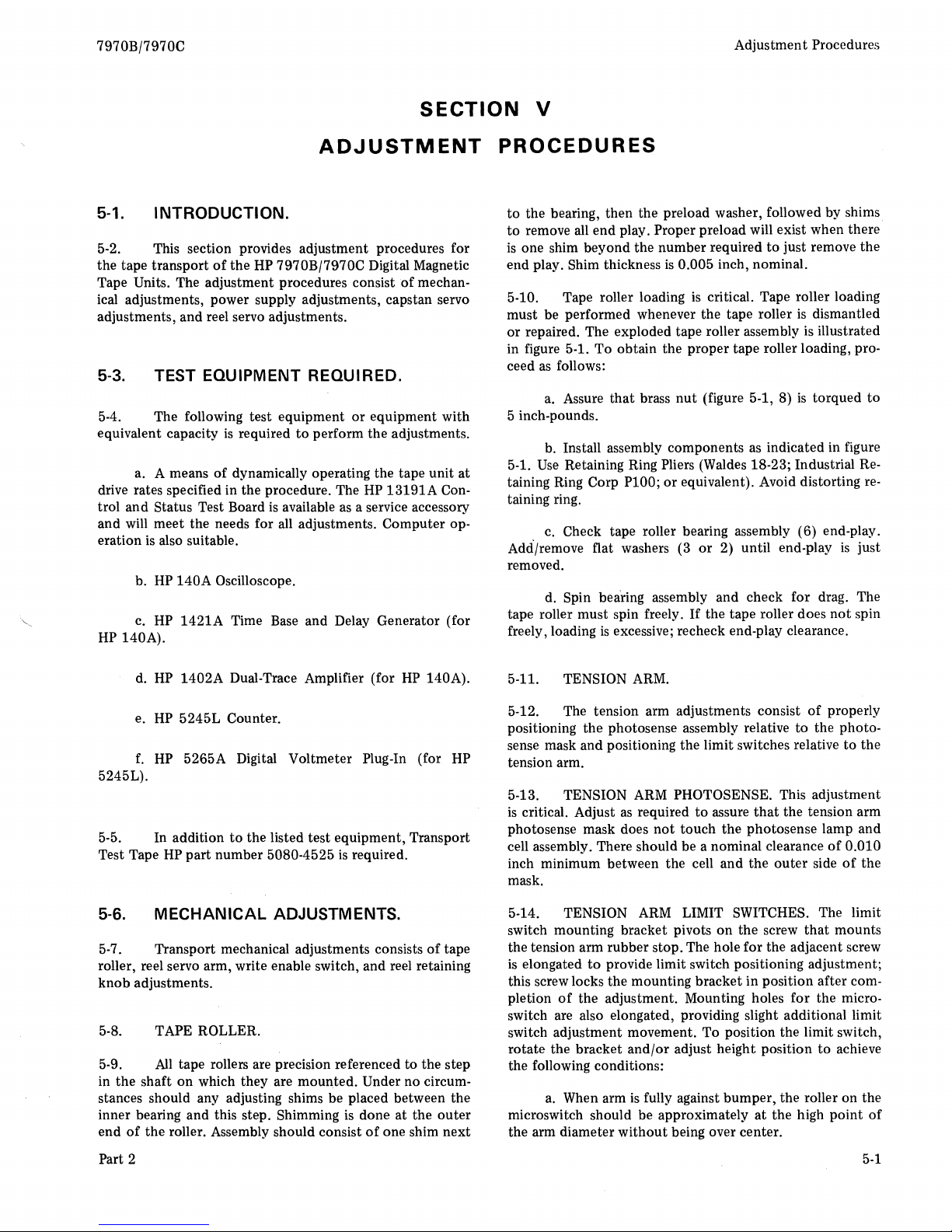
7970Bj7970C Adjustment Procedures
SECTION
ADJUSTMENT
5-1. INTRODUCTION.
5-2. This section provides adjustment procedures for
the tape transport
Tape
Units. The adjustment procedures consist
ical adjustments, power supply adjustments, capstan servo
adjustments, and reel servo adjustments.
5-3. TEST EQUIPMENT REQUIRED.
5-4. The following test equipment
equivalent capacity
a. A means
drive rates specified in the procedure. The
trol
and
Status Test Board
and will meet the needs for all adjustments. Computer
eration
HP 140A).
is
also suitable.
b.
HP
c. HP
140A
1421A
of
the
HP 7970Bj7970C Digital Magnetic
of
mechan-
or
equipment with
is
required
of
dynamically operating the tape unit
Oscilloscope.
Time Base and Delay Generator (for
to
perform the adjustments.
HP
is
available
as
a service accessory
13191A
at
Con-
op-
V
PROCEDURES
to
the bearing, then the preload washer, followed by shims
to
remove all end play. Proper preload will exist when there
is
one shim beyond the number required
end play.
5-10. Tape roller loading
must
or
in figure 5-1. To obtain the proper tape roller loading,
ceed
5 inch-pounds.
5-1.
taining Ring Corp P100;
taining ring.
Add'/remove flat washers (3
removed.
tape roller must spin freely.
freely, loading
Shim thickness
be performed whenever the tape roller
repaired. The exploded tape roller assembly
as
follows:
a.
Assure
that
b.
Install assembly components
Use
Retaining Ring Pliers (Waldes 18-23; Industrial Re-
c. Check tape roller bearing assembly
d.
Spin bearing assembly and check for drag. The
is
excessive; recheck end-play clearance.
is
0.005 inch, nominal.
is
critical. Tape roller loading
brass
nut
(figure 5-1, 8)
or
equivalent). Avoid distorting
or
2) until end-play
If
the tape roller does
to
just remove the
is
dismantled
is
illustrated
is
torqued
as
indicated in figure
(6)
end-play.
is
not
pro-
to
re-
just
spin
d.
HP
1402A
e.
HP 5245L Counter.
f.
HP
5245L).
5-5. In addition
Test Tape
5-6.
5-7. Transport mechanical adjustments consists
roller, reel servo arm, write enable switch, and reel retaining
knob
5-8.
5-9.
in the shaft
stances should any adjusting shims be placed between the
inner bearing and this step. Shimming
end
HP
MECHANICAL ADJUSTMENTS.
adjustments.
TAPE ROLLER.
All
tape rollers are precision referenced
on
of
the roller. Assembly should consist
Dual-Trace Amplifier (for
5265A Digital Voltmeter Plug-In (for HP
to
the listed test equipment, Transport
part number 5080-4525
which they are mounted. Under no circum-
is
required.
is
HP
to
the step
done at the
of
one shim next
140A).
of
tape
outer
5-11.
5-12. The tension arm adjustments consist
positioning
sense mask and positioning the limit switches relative
tension arm.
5-13.
is
photosense mask does
cell assembly. There should be a nominal clearance
inch minimum between the cell and the
mask.
5-14.
switch mounting bracket pivots
the tension arm rubber stop. The hole for the adjacent screw
is
this screw locks the mounting bracket in position after
pletion
switch are also elongated, providing slight additional limit
switch adjustment movement. To position the limit switch,
rotate
the following conditions:
microswitch should be approximately
the arm diameter
TENSION ARM.
the
photosense assembly relative to the photo-
TENSION ARM PHOTOSENSE. This adjustment
critical. Adjust
TENSION ARM LIMIT SWITCHES. The limit
elongated
of
the bracket
a.
When arm
as
required
to
provide limit switch positioning adjustment;
the adjustment. Mounting holes for the micro-
and/or
is
fully against bumper, the roller on the
without
to
assure
that
not
touch
the photosense lamp and
on
the screw
adjust height position
at
being over center.
the tension arm
outer
the high
of
side
that
to
properly
to
the
of
0.010
of
the
mounts
com-
achieve
point
of
Part 2
5-1
Page 24
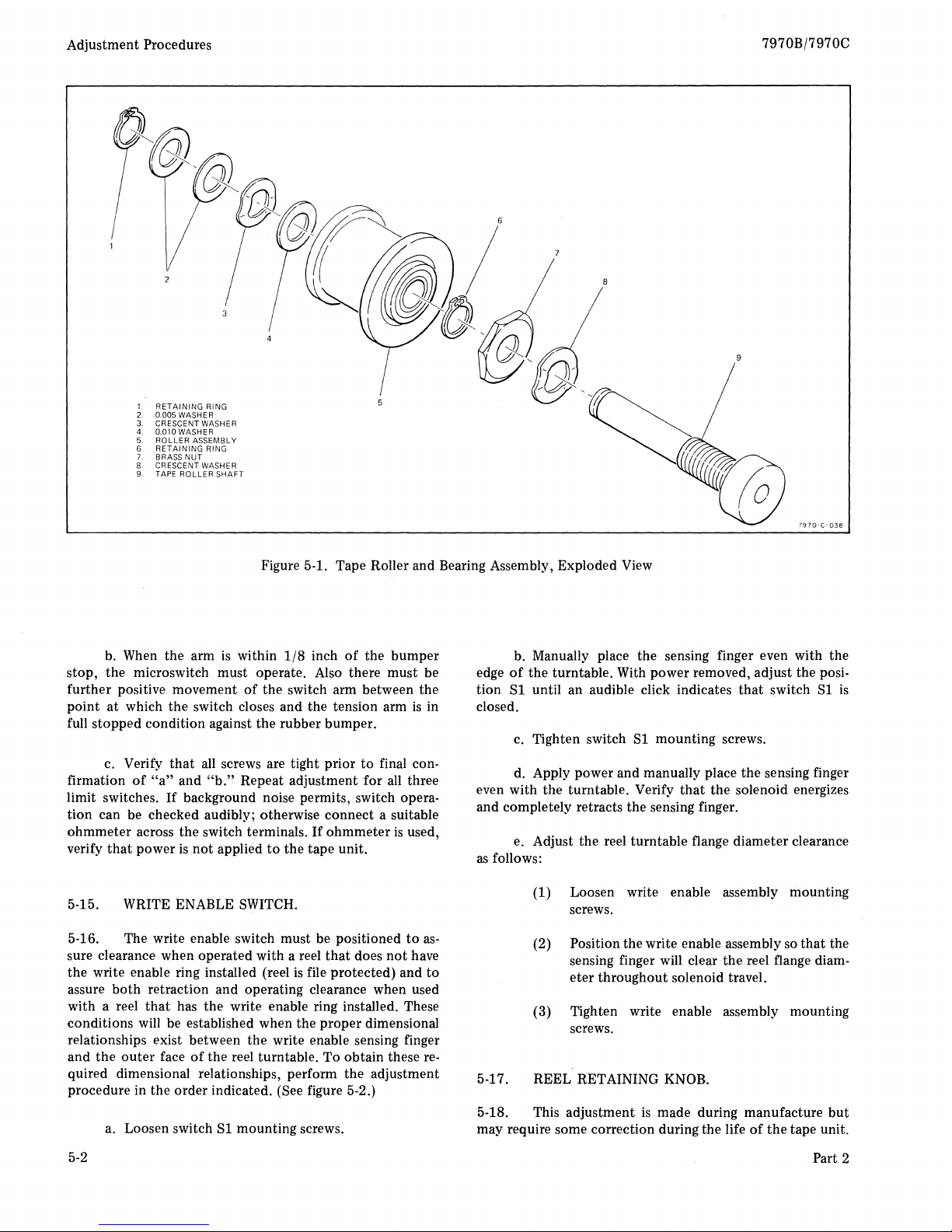
Adjustment Procedures
1
RETAINING
2 0.005 WASHER
3.
CRESCENT WASHER
0.010 WASHER
4
ROLLER
RETAINING
BRASS
NUT
TAPE
ROLLER
ASSEMBLY
5
G
7.
8 CRESCENT WASHER
9.
7970B/7970C
RING
RING
SHAFT
Figure 5-1. Tape Roller and Bearing Assembly, Exploded View
b.
When the arm
is
within
1/8
inch
of
the bumper
stop, the microswitch must operate. Also there must be
further positive movement
point
at
which the switch closes and the tension arm
of
the switch arm between the
is
in
full stopped condition against the rubber bumper.
c. Verify
firmation
limit switches.
of
that
all
screws are tight prior
"a"
and
"b."
Repeat adjustment for all three
If
background noise permits, switch opera-
to
final con-
tion can be checked audibly; otherwise connect a suitable
ohmmeter
verify
5-15.
5-16. The write enable switch must be positioned
sure clearance when operated with a reel
the write enable ring installed (reel
assure
with a reel
across the switch terminals.
that
power
is
not
applied
If
to
the tape unit.
ohmmeter
WRITE ENABLE SWITCH.
that
is
file protected) and
both
retraction and operating clearance when used
that
has the write enable ring installed. These
does
is
not
used,
to
as-
have
to
conditions will be established when the proper dimensional
relationships exist between the write enable sensing finger
and
the
outer
face
of
the reel turntable. To obtain these required dimensional relationships, perform the adjustment
procedure
in
the order indicated. (See figure 5-2.)
a.
Loosen switch
Sl
mounting screws.
b. Manually place the sensing finger even with the
edge
of
the turntable. With power removed, adjust the posi-
tion
Sl
until an audible click indicates
that
closed.
c. Tighten switch
Sl
mounting screws.
d. Apply power and manually place the sensing finger
even with the turntable. Verify
that
the solenoid energizes
and completely retracts the sensing finger.
e. Adjust the reel turntable flange diameter clearance
as
follows:
(1) Loosen write enable assembly mounting
screws.
(2) Position the write enable assembly so
sensing finger will clear the reel flange
eter throughout solenoid travel.
(3) Tighten write enable assembly mounting
screws.
5-17.
5-18. This adjustment
may require some correction during the life
REEL RETAINING
is
KNOB.
made during manufacture
of
switch
the
tape unit.
7970-C-038
Sl
that
diam-
is
the
but
5-2
Part 2
Page 25
7970B/7970C
WRITE
SENSING
ENABLE
FINGER
SWITCH
MOUNTING
WRITE
ENABLE
(ENERGIZES
SCREWS
SWITCH
SOLENOIDI
Adjustment Procedures
Sl
7970-506
Figure 5-2. Write Enable Assembly
is
When the locking lever
possible
of
to
place the reel over the rubber with a minimum
interference. When the locking lever
resistance should be encountered
sed. In the locked position,
move the reel by hand.
piece
of
masking tape
mark placed in alignment
not become misaligned by more than
of
operation. To correct tape reel slippage, release locking
working properly,
as
it
should
If
slippage
on
the reel, another
on
both
the rubber
is
pieces
1/8
it
should be
is
closed, positive
is
compres-
not
be possible
to
suspected, place a
on
the hub. A
of
tape should
inch in
16
hours
lever and loosen the pozidrive screw, rotate the reel retainer
knob clockwise, and tighten screw. Repeat until tape reel
mounts firmly and does
not
slip.
5-19. ELECTRICAL ADJUSTMENTS.
5-20. The electrical adjustments
critical and must be performed in the following sequence:
a.
Power supply adjustments.
b.
Capstan
Capstan servo forward and reverse drive speed ad-
c.
motor
offset current adjustment.
justments.
d.
Capstan servo high-speed forward adjustment.
e.
Capstan servo high-speed reverse adjustment.
f. Capstan servo ramp slope adjustment.
g.
Reel servo adjustments.
of
the tape unit are very
WRITE
ENABLE
SWITCH
S2
5-21.
5-22. Only one adjustment
lated supplies. The adjustment control
cuitry for the +12 volt supply
the value
operating tolerance. The value
plies
trol
bly. Voltage
POWER SUPPLY ADJUSTMENTS.
is
provided for the three regu-
is
but
is
adjusted
of
the +5 volt supply, which
of
the +12 and
is
established by a precision resistor network. The con-
is
located
on
the power regulator printed-circuit assem-
is
correctly adjusted when the following con-
ditions are met:
a.
+5
justment
b.
c.
± 0.050 Vdc. (Adjust
is
required.)
+12 ± 0.360 Vdc.
-12
± 0.360 Vdc.
to
±0.010 Vdc when ad-
Note
Final reel servo adjustments must be made after
the capstan servo adjustments. The capstan speed
must be within tolerance in order
adjust
the
reel servo. However, tension
maintained in order
adjustments.
If
to
make the capstan servo
the tape unit does
tension, perform the reel servo adjustments
tially, complete the capstan servo adjustments,
and repeat the reel servo adjustments.
located in the cir-
to
establish
is
held
to
a tighter
-12
volt sup-
to
properly
must
be
not
maintain
ini-
Part 2
5-3
Page 26
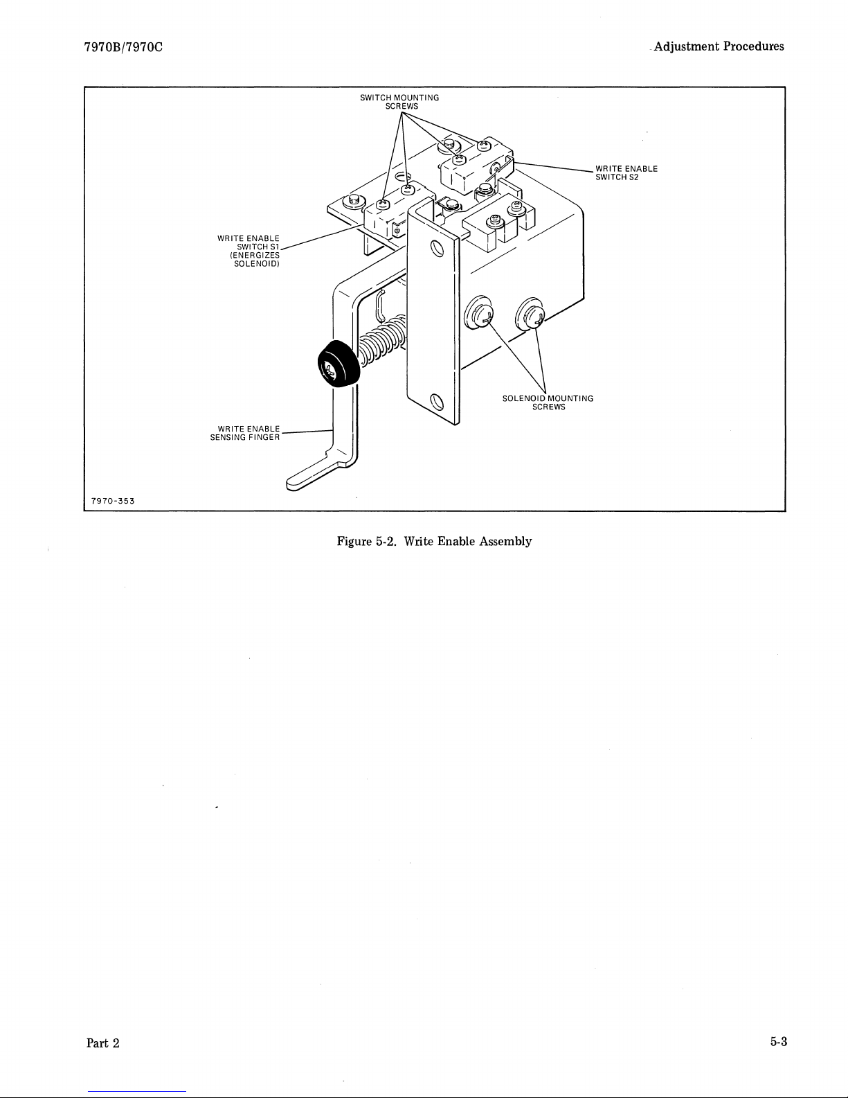
7970Bj7970C
WRITE ENABLE
SWITCH
(ENERGI
SOLENOIO)
WRITE
ENABLE
SENSING FINGER
..
Adjustment Procedures
SWITCH MOUNTING
SCREWS
WR
ITE ENABLE
SWITCH
S2
S1
___
--I
7970-353
Figure 5-2.
Write
Enable Assembly
Part
2
5-3
Page 27
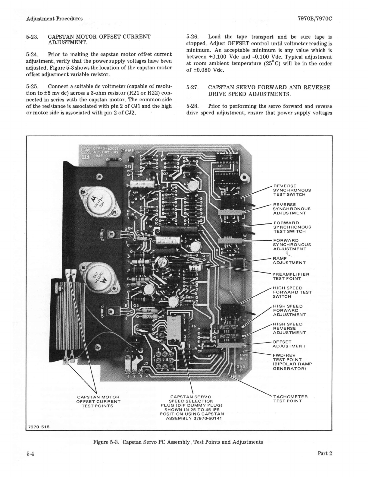
Adjustment Procedures
5-23. CAPSTAN MOTOR OFFSET CURRENT
ADJUSTMENT.
5-24. Prior
to
making the capstan
motor
offset current
adjustment, verify
that
the power supply voltages have been
adjusted. Figure
5-3 shows the location
of
the capstan
motor
offset adjustment variable resistor.
5-25. Connect a suitable dc voltmeter (capable
of
resolu·
tion
to
±5 mv dc) across a 3-ohm resistor (R21
or
R22) con·
nected in series with the capstan
motor
. The common side
of
the resistance
is
associated with pin 2
of
CJ1 and the high
or
motor
side
is
associated with pin 2
of
CJ2.
7970B/7970C
5-26.
Load the tape transport and be sure tape
is
stopped. Adjust OFFSET control until voltmeter reading
is
minimum. An acceptable minimum
is
any value which
is
between +0.100 Vdc and
-0.100
Vdc. Typical adjustment
at room ambient temperature (25°
C)
will be in the order
of
±0.080 Vdc.
5-27. CAPSTAN SERVO FORWARD AND REVERSE
DRIVE SPEED ADJUSTMENTS.
5-28. Prior to performing the servo forward and reverse
drive speed adjustment , ensure
that
power supply voltages
REVERSE
SYNCHRONOUS
TEST
SWITCH
REVERSE
SYNCHRONOUS
ADJUSTMENT
___
FORWARD
SYNCHRONOUS
TEST
SWITCH
---FORWARD
SYNCH
RONOUS
ADJUSTMENT
RAMP
ADJUSTMENT
PREAMPLIFIER
TEST POI
NT
HIGH
SPEED
FORWARD
TEST
SWITCH
HIGH
SPEED
FORWARD
ADJUSTMENT
HIGH
SPEED
REVERSE
ADJUSTMENT
OFFSET
ADJUSTMENT
FWD/REV
TEST
POINT
(BIPOLAR
RAMP
GENERATOR)
CAPSTAN
SERVO
SPEED
SELECTION
PLUG
(DIP
DUMMY
PLUG
)
SHOWN
IN
25
TO
45
IPS
POSITION
USING
CAPSTAN
ASSEM
BL
Y
07970-60141
TACHOMETER
TEST
POINT
7970-518
Figure 5-3. Capstan Servo
PC
Assembly, Test Points and Adjustments
5-4
Part 2
Page 28
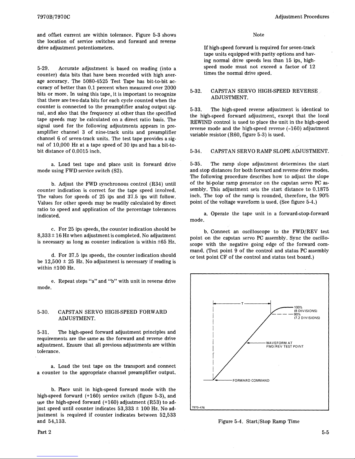
7970B/7970C
Adjustment Procedures
and offset current are within tolerance. Figure 5-3 shows
the location
of
service switches and forward and reverse
drive adjustment potentiometers.
is
5-29. Accurate adjustment
counter) data bits that have been recorded with high
age
accuracy. The 5080-4525 Test Tape has bit-to-bit
curacy
of
better than 0.1 percent when measured over 2000
bits
or
more. In using this tape, it
that
there are two data bits for each cycle counted when the
is
counter
connected
nal, and also
that
to
the
the frequency
based on reading (into a
is
important
to
preamplifier analog
at
other
than the specified
aver-
recognize
output
ac-
sig-
tape speeds may be calculated on a direct ratio basis. The
signal used for the following adjustments appears in
preamplifier channel 3 of nine-track units and preamplifier
channel 6
nal
bit distance
mode using
counter indication
The values for speeds
of
seven-track units. The test tape provides a
of
10,000
a.
b. Adjust the
Hz
at
of
0.0015 inch.
a tape speed
of
30 ips and has a bit-to-
Load test tape and place unit in forward drive
FWD
service switch (S2).
FWD
synchronous control (R34) until
is
correct for the tape speed involved.
of
25
ips and 37.5 ips will follow.
sig-
Values for other speeds may be readily calculated by direct
ratio
to
speed and application
of
the percentage tolerances
indicated.
c. For 25 ips speeds, the counter indication should be
8,333 ±
is
necessary
Hz when adjustment
as
long
as
counter indication
is
completed.
No
adjustment
is
within ±65
Hz.
16
d. For 37.5 ips speeds, the counter indication should
be
12,500
within ±100
± 25
Hz.
Hz.
No adjustment
is
necessary if reading
is
Note
If
high-speed forward
tape units equipped with parity options and
is
required for seven-track
having normal drive speeds less than 15 ips, highspeed mode must
not
exceed a factor
of
12
times the normal drive speed.
5-32.
CAPSTAN SERVO HIGH-SPEED REVERSE
ADJUSTMENT.
5-33. The high-speed reverse adjustment
the high-speed forward adjustment, except
is
REWIND control
used to place the
reverse mode and the high-speed reverse
variable resistor
5-34.
CAPSTAN SERVO RAMP SLOPE ADJUSTMENT.
(R60, figure 5-3)
is
used.
unit
is
that
in
the
(-160)
identical
the local
high-speed
adjustment
to
5-35. The ramp slope adjustment determines the start
both
and stop distances for
The following procedure describes how
of
the bi-polar ramp generator on the capstan servo
sembly. This adjustment sets the start distance
inch. The
point
top
of
the ramp
ofthe
voltage waveform
a.
Operate the tape unit in a forward-stop-forward
forward and reverse drive modes.
to
adjust the slope
PC
as-
to
0.1875
is
rounded, therefore, the 90%
is
used. (See figure 5-4.)
mode.
b. Connect an oscilloscope
point
on the capstan servo
scope with the negative going edge
mand. (Test
or
test point CF
point 9 of
of
the control and status
the control and status test board.)
to
the FWD/REV test
PC
assembly. Sync the oscillo-
of
the forward com-
PC
assembly
e. Repeat steps
"a"
and
"b"
with unit in reverse drive
mode.
5-30.
CAPSTAN SERVO HIGH-SPEED FORWARD
ADJUSTMENT.
5-31. The high-speed forward adjustment principles and
requirements are the same
adjustment. Ensure
as
the forward and reverse drive
that
all previous adjustments are within
tolerance.
on
a. Load the test tape
to
a counter
the appropriate channel preamplifier
the transport and connect
output.
b. Place unit in high-speed forward mode with the
high-speed forward
use the high-speed forward
just speed until counter indicates 53,333 ±
justment
is
required if counter indicates between 52,533
(+160) service switch (figure 5-3), and
(+160) adjustment (R53)
100
Hz.
to
ad-
No ad-
and 54,133.
Part 2
7970-476
1-1.
---T-----I"I
----90%
/----WAVEFORM
~FORWARDCOMMAND
FWD/REV TEST POINT
Figure 5-4. Start/Stop Ramp Time
AT
100%
18
DIVISIONS)
17.2
DIVISIONS)
5-5
Page 29
Adjustment Procedures
c. Adjust the capstan servo
trol (See figure 5-3.)
to
obtain the time listed in table 5-1
for tape unit synchronous speed.
control
the 90%
of
the oscilloscope
point
may be conveniently measured.
to
Note
On
HP
180 Oscilloscopes, the vertical spacing
a special horizontal time scale
which may be used
to
measure the time
90% level.
Table 5-1. Capstan Servo Start/Stop Time
SPEED (IPS)
12.5 26.1
18.75
22.5
25
37.5 8.1
45
PC
assembly RAMP con-
Use
the vertical gain vernier
expand the waveform so
is
at
7.2 divisions
at
the
TIME
(90%)
ms
17.1ms
14.1
ms
12.6
ms
ms
6.6
ms
that
7970B/7970C
5-36. REEL SERVO ADJUSTMENTS.
5-37. Load a short length
bring
to
load point. The following adjustments determine
the peak deflections
deflection desired
of
is
a function
At the highest speed (45 ips) the deflection
tension arms deflect
side
of
the casting,
At lower speeds the
25 ips the deflection
ips). Due
swing
to
non-linearity
of
the tension arm may be unsymmetrical in the for-
to
both
amount
is
of
tape
onto
the transport and
the tension arms. The amount
of
the synchronous speed.
is
set so the
the
outer
marks located on the back
in forward and reverse drive modes.
of
deflection
about
half (25/45) the
of
the tension arm transducer the
is
smaller (Le.,
amount
at
of
at
45
ward and reverse drive modes. (This will mean the tension
arm will
is
200 feet
not
be centered when there
is
no tape motion and
normal.) With the supply reel loaded with approximately
of
tape, rotate the supply (upper) variable resistor
(R106) fully clockwise and run the tape unit in the forward
mode. Rotate the supply (lower) variable resistor
clockwise for the proper deflection.
put
in reverse drive and make sure the
is
the same
as
in forward drive.
position until symmetrical swings
If
of
Stop
tape motion and
amount
not,
readjust the mask
the
proper
achieved. Repeat procedure for the take up reel with
mately 200 feet
of
tape on the takeup reel.
counter-
of
deflection
amount are
approxi-
5-6
Part 2
Page 30
7970B/7970C
Replaceable Parts
SECTION
VI
REPLACEABLE
PARTS
6-1.
INTRODUCTION.
6-2. This section provides information for ordering replacement parts for the tape transport
of
the HP 7970B /
7970C Digital Magnetic Tape
Units.
6-3. This section contains assembly parts lists, support-
ing illUstrations, ordering information, and a
part
number
cross reference.
6-4. ASSEMBL Y PARTS LIST.
6-5. The assembly parts list presents a breakdown
of
all
replaceable parts
of
the tape transport. The information
contained in the lists are under the following headings:
a.
FIGURE & INDEX NO.
b. PART
NUMBER.
c. DESCRIPTION.
d.
UNITS PER ASSY.
6-6. FIG
URE AND INDEX NUMBER.
6-7. The figure and index number column identifies the
figure
that
illustrates each listed item and the index number
that
identifies the item
on
the illustration.
6-8. PART
NUMBER.
6·9 .
The
part
number column provides the Hewlett-
Packard
part
number for each item listed in
the
assembly
parts list.
6·10. DESCRIPTION.
6-11. The description column describes the items within
the equipment. An indented column arrangement
is
used
to
show the relationship between a part and
the
parts next
higher assembly. The
top
assembly
of
each listing appears in
Part 2
indention 1. Primary subassemblies
(of
the
top
assembly)
and attaching parts appear in indention 2. This method
of
indention is continued through indention 3, 4, etc, until all
replaceable parts are listed. Attaching parts are listed
im-
mediately following the
part
they attach. Attaching parts
are identified by the abbreviation (AP) enclosed
in
paren-
thesis at the end
of
the description.
6-12. Reference designation and manufacture
informa-
tion (if applicable)
is
also included in the description col-
umn.
6·13. UNITS PER ASSEMBLY.
6·14. The
quantity
shown in the units per assembly col-
umn
reflects the total quantity
of a part
required by the
next higher assembly
of
that
part. This
quantity
is
not
neces-
sarily the total used for the complete equipment. The ab-
breviation AR
is
used
to
indicate usage
as
required
of
a
particular item. The abbreviation
REF
is
used
to
indicate
that
the quantity
of
an item used
per
assembly
is
listed in
the next higher assembly
of
the assembly
part~
list.
6-15.
ORDERING
INFORMATION.
6·16. To order replacement parts, address the
order
or
inquiry
to
the local Hewlett-Packard Sales and Service Office.
(Refer
to
the list
at
the end
of
this manual for addresses.)
Specify the following information for each
part
ordered.
a. Identification
of
the unit, kit,
or
assembly con-
taining the part.
b. Hewlett-Packard
part
number for each part.
c. Description
of
each part.
d. Circuit reference designation (if applicable).
6-17. PART NUMBER CROSS REFERENCE.
6-18. Table 6-1
at
the end
of
this section provides a
cross reference between Hewlett-Packard
part
numbers and
manufacturer's
part
numbers .
6-1
Page 31

7970B/7970C Replaceable Parts
SECTION
REPLACEABLE
6-1. INTRODUCTION.
6-2. This section provides information for ordering re-
of
the
HP
placement parts for the tape transport
7970C
Digital Magnetic Tape Units.
6-3. This section contains assembly parts lists, supporting illustrations, ordering information, and a part number
cross reference.
6-4. ASSEMBLY PARTS LIST.
6-5. The assembly parts list presents a breakdown
replaceable parts
contained in the lists are under the following headings:
a. FIGURE
b. PART NUMBER.
c.
DESCRIPTION.
of
the tape transport. The information
& INDEX NO.
7970B/
of
all
VI
PARTS
indention 1. Primary subassemblies (of the
and attaching parts appear in indention 2. This method
indention
replaceable parts are listed. Attaching parts are listed immediately following the part they attach. Attaching parts
are identified by the abbreviation
thesis
6-12. Reference designation and manufacture information (if applicable)
umn.
6-13.
6·14.
umn reflects the total quantity
next higher assembly
sarily the total used for the complete equipment. The abbreviation AR
particular item. The abbreviation
that
the next higher assembly
is
continued through indention 3, 4, etc, until all
(AP) enclosed in paren-
at
the end
UNITS PER ASSEMBLY.
The quantity shown in the units per assembly col-
the quantity
of
the description.
is
also included in the description col-
of
a part required by the
of
that
part. This quantity
is
used to indicate usage
REF
of
an item used per assembly
of
the assembly parts list.
is
top
as
required
used
assembly)
is
not
to
indicate
is
listed in
of
neces-
of
a
d.
UNITS PER ASSY.
6-6. FIG URE
6-7. The figure and index number column identifies the
figure
that
that
identifies the item on the illustration.
6-8.
6-9. The part number column provides the HewlettPackard
parts list.
6-10. DESCRIPTION.
6-11. The description column describes the items within
the equipment.
show the relationship between a part and the parts next
higher assembly. The top assembly
PART NUMBER.
part
AND
INDEX NUMBER.
illustrates each listed item .and the index number
number for each item listed in
An
indented column arrangement
of
each listing appears in
the
assembly
is
used
to
6-15. ORDERING INFORMATION.
6-16. To order replacement parts, address
inquiry
(Refer
Specify the following information for each
taining the part.
6-17. PART NUMBER
6-18. Table
cross reference between
manufacturer's part numbers.
to
the local Hewlett-Packard Sales and Service Office.
to
the list
a.
Identification
b.
Hewlett-Packard
c. Description
d. Circuit reference designation (if applicable).
6-1
at
the end
of
part
of
each part.
at
the end
Hewlett-Packard
of
this manual for addresses.)
part
the unit, kit,
number for each part.
CROSS
of
or
REFERENCE.
this section provides a
part
the
order
or
ordered.
assembly con-
numbers and
Part 2
6-1
Page 32

· Replaceable Parts
17
19
20
13
8
10
11
12
9
13
14
15
16
7970-514A
6-2
6
7
5
1C
1A
Figure 6-1.
7970Bj7970C
Digital Magnetic Tape Unit (Sheet 1
of
3)
16
7970Bj7970C
1G
1E
1F
1H
Part 2
Page 33

7970B/7970C
41
42
40
49
50
51
52
53
97
98
99
93
43
94
95
96
44
45
40
41
42
7970-516
Part 2
36
37
38
39
22
26
23
272524
21
44
45
43
48
49
47
50
48
51
49
52
46
50 53
Figure 6-1. 7970B/7970C Digital Magnetic Tape Unit (Sheet 2
of
3)
55
57
59
60
Replaceable Parts
63
65
62
64
61
28
28
56
57
58
54
72
73
71
66
67
68
69
70
75
76
74
80
81
82
77
29
78
79
129
130
131
132
133
134
3034
31
35
32
33
84
85
83
6-3
Page 34

Replaceable Parts
125
126
__
",*
w .
127
128
123
124
7970-515
6-4
100
101
102
103 104
105
106
107
108
Figure 6-1. 7970B/7970C Digital Magnetic Tape Unit (Sheet 3
of
3)
119
118
120
121
7970B/7970C
113
Part 2
Page 35

7970B/7970C
Replaceable Parts
FIGURE
&
INDEX
NO.
6-1-
-1
-lA
-lB
-lC
-10
-1
E
-1
F
-lG
-lH
-2
-3
-4
-5
-6
-7
-8
-9
-10
-11
-12
-13
-14
-15
-16
-17
-18
-19
-20
-21
-22
-23
-24
-25
-26
-27
-28
-29
-30
-31
PART
NUMBER
1 2 3
7970B/7970C
07970-60160
07970-20B30
2200-0139
07970-20832
07970-01186
07970-20831
0624-0208
0510-1107
07970-20829
07970-60010
2190-0003
2200-0139 SCREW, no. 4-40, 0.25-inch, pozi (AP)
07970-20480
2190-0003 WASHER, lock, helical (AP)
2200-0139 SCREW, no. 4-40, 0.25-inch, pozi (AP)
07970-01000
07970-01010
07970-01020
07970-01030
07970-01040
07970-01050
07970-01
07970-01070
07970-01160
07970-00130
07970-60130
07970-60140
07970-60141
07970-20070
07970-01204 SPACER, hinge
07970-20470
2680-0104
07970-62106 DOOR STOP ASSEMBLY
2190-0034
2190-0420
2190-04i5
07970-20120
2190-0034
2680-0065
.07970-60890
07970-00510
2190-0416
0380-0013 SPACER (AP) .
060
3050-0065
2190-0034 WASHER, lock, helical (AP)
2680-0103
2190-0429
3030-0047
4 5
DIGITAL
COVER
INSERT,
SCREW,
WINDOW,
PANEL,
HANDLE,
SCREW,
FASTENER,
FRAME,
PANEL,
PANEL,
PANEL,
PANEL,
PANEL,
PANEL,
PANEL,
PANEL,
PANEL,
COVER,
TAPE
CAPSTAN
CAPSTAN MOTOR ASSEMBLY
HINGE
HINGE,
BLOCK,
RIBBON
GROUND
DOOR
cover
no.4-40,
cover
cover
cover
tapping, no. 6-32, 0.5-inch, pozi (AP)
cover
HINGE
ASSEMBLY,
WASHER, lock, helical
HINGE,
units
WASH
SCREW,
and attaching parts)
WASHER, lock, helical
SCREW,
SCREW,
WASH
WASH
WASHER, nylon (AP)
WASHER, lock, helical
SCREW,
WASHER,
cover
switch cover
only)
switch cover (density select and
switch cover
switch cover
switch cover
switch cover (density select equipped
switch cover
switch cover (basic
switch cover (read/read
head
ER,
no. 6-32, 0.5-inch, pozi (AP) •
ROLLER
MOTOR
no. 10-32, 0.625-inch, socket head (AP)
BLOCK,
transport
no. 10-32, 0.5-inch, pozi (AP)
ER, lock, helical
ER,
door
no. 10-32, 1.25-inches, pozi
CABLE
STRAP.
MAGNETIC
ASSEMBLY
door.
0.25-inch, pozi (AP) 12
door
door.
door
panel
door
door
(unit
(unit
(write
(unit
(unit
assembly.
flat
(AP)
AND
BEARING
ASSEMBLY MG1, 10 - 37.5 ips
mounting
flat
(AP)
stop
ASSEMBLY W5
flat
(AP)
DESCRIPTION
TAPE
door
stop
(AP)
address, density select,
address and
enable equipped
address and density select equipped
select equipped
unit
(AP).
(AP).
(AP).
write
only),
units
only)
ASSEMBLY
MG1,
37.6 -
UNIT.
write
write
enable equipped
enable equipped units
units
only)
units
only)
units
only)
.
(see
figure 6-2
(see
45
ips
(see
(AP).
enable equipped
units
only)
only)
units
only)
for
details.
figure 6-3
figure 6-4
for
for
details)
details)
UNITS
PER
ASSV
REF
1
1
1
1
1
2
2
1
1
4
4
2
10
10
1
1
1
1
1
1
1
1
1
1
2
2
2
2
1
1
4
4
2
2
2
5
1
2
2
2
1
2
2
2
1
1
1
Part
2
6-5
Page 36

Replaceable Parts
7970B/7970C
FIGURE
&
INDEX
PART
NUMBER
NO.
6-1-32
-33
-34
-35
-36
-37
-38
-39
-40 07970-60170
-41
-42
-43
-44
-45
-46
-47
·48
-49
-50
-51
-52
-53
-54
-55
·56
-57
-58
-59
-60
-61
-62
-63
-64
-65
-66
-67
-68
-69
-70
-71
-72
-73
-74
-75
-76
2190-0003
2190-0008 WASHER, lock, external (AP)_ 1
07970-00610
2200-0125 SCREW, no. 4-40, 1.5-inches, pozi (AP) 1
07970-62122
2190-0416
2190-0003 WASHER, lock, helical (AP) 3
2200-0125 SCREW,
07970-60171
2190-0432 WASHER, lock, helical (AP) 4
0570-0082
07970-60181 TENSION
2190-0034
2680-0105 SCREW, no. 10-32, 0.625·inch, pozi (AP) 3
07970-01190
0380-1012
2190-0420 WASH ER,
2190·0034 WASHER, lock, helical (AP)
2680-0111 SCREW,
07970-01191 WASHER, bumper
4320-0256
07970-20834
07970-00120
0380-0016
3050-0002 WASHER,
2190-0034
2680-0099
2680-0103 SCREW, no. 6-32, 0.5-inch, pozi (AP)
0403-0163
07970-62089
2190-0034 WASHER, lock, helical (AP)
2190-0003 WASHER, lock, helical (AP)
2680-0129
2200-0143
07970-61150
07970-01176
3050-0105
2190-0003 WASHER, lock, helical (AP)
2200-0141
07970-60500
07970-62000
07970-62001
07970-62012
2190-0034
2680-0103
07970-60300
07970·62165
07970-60300
2190-0034
2680-0099
1
.
4
2 3
WR
REEL
REEL
BRACKET,limit
BRACKET,
CONTROL
PHOTOSENSE
READ
READ
READ/READ
READ/READ
WRITE
WRITE
WRITE
5
WASHER,lock,
GUIDE,
ITE
ENABLE
ER,
WASH
MOTOR
MOTOR
SCREW,
WASHER,lock,
SPACER
EXTRUSION,
GUIDE,
SPACER
WASHER,lock,
SCREW,
BUMPER, stop (AP)
SCREW,
SCREW,
INSULATOR,
WASH
ER,
SCREW,
PREAMPLIFIER
PREAMPLIFIER
WASHER,lock,
SCREW,
INTERCONNECT
INTERCONNECT
INTERCONNECT
WASHER, lock, helical
SCREW,
DESCRIPTION
helical (AP) 1
cable (AP) _
ASSEMBLY
flat
(AP) _
no_
4-40, 1.5-inches, pozi (AP)
ASSEMBLY
ASSEMBLY B 1/B2
no. 5/16-18,
ARM
ASSEMBLY
helical (AP) 3
switch,
(AP)
flat
(AP) .
no. 10-32, 1.O-inch, pozi (AP)
rubber
bumper.
limit
switch,
(AP)
flat
(AP) .
helical (AP)
no. 10-32, 0.375-inch, pozi (AP)
SWITCH
no. 10-32, 0.132-inch, pozi (AP)
no. 4-40, 0.375-inch, pozi (AP) .
no. 4-40, 0.312-inch, pozi (AP) .
no. 6-32, 0.5-inch, pozi (AP)
no. 10-32, 0.375-inch, pozi (AP)
ASSEMBLY
HEAD
photosense .
flat
(AP) .
PREAMPLIFIER
PREAMPLIFIER
helical (AP)
A 10 (refer
Bl/B2,
10 -
(see
l-inch
(AP)_ 4
A3/A4
(see
upper
lower
All
(see
ASSEMBL Y
ASSEMBLY
ASSEMBLY
ASSEMBLY
ASSEMBLY
ASSEMBLY A 1421 -45
(AP)
A2
(see
A15, 10 - 20.9 ips (refer
A15,
ASSEMBLY
ASSEMBLY
A14
A14
to
part 4 for
37_5
ips
figure 6-5
figure 6-6
figure 6-7
figure 6-8
21 -45
A15, 10 - 20.9 ips (refer
A15,
(refer
10 - 20.9 ips (refer
details) 1
(see
figure 6-5
for
details) 2
for
details)
for
details).
for
details)
ips
(refer
21-45
ips (refer
;
to
part
4) .
ips (refer
to
to
to
for
part
part
to
part
details)
3)
3) .
to
to
part
4l.
part
part
4)
UNITS
PER
ASSV
1
3
3
2
2
1
1
2
2
2
1
1
1
2
1
1
2
1
1
1
1
2
1
2
1
1
1
2
2
2
1
1
5)
5)
.
1
1
2
2
1
1
1
2
2
6-6
Part 2
Page 37

7970B/7970C
Replaceable Parts
FIGURE
&
INDEX
NUMBER
NO.
6-1-77
-78
-79
-80
-81
-82
-83
-84
-85
-86
-87
-88
-89
-90 2680-0101
-91
-92
-93
-94
-95
-96 2680-0101
-97
-98
-99
-100
-101
-102
-103
-104
-105
-106
-107
-108
07970-60580
07970-60581
07970-60582
07970-60583
07970-60584
07970-62031
07970-60586
07970-60587
07970-60588
07970-60589
2190-0034
3030-0038
07970-62087
07970-62088
2190-0034
2680-0129
07970-62086
2190-0034
2680-0129
07970-60600
07970-62172
2190-0034
2190-0312
07970-20680
2680-0118
07970-62024
2190-0312
2190-0034
1390-0228
2190-0034
2680-0099
07970-60230
2190-0085
3050-0016
2360-0195
07970-60900
07970-60890
07970-60390
07970-62003
2190-0085
3050-0016
2360-0195
PART
DESCRIPTION
1 2 3 4
MAGNETIC
MAGNETIC
MAGNETIC
MAGN
MAGN
MAGNETIC
MAGNETIC
MAGNETIC
MAGN
MAGN
DENSITY
DENSITY
UN
TRANSPORT
CAPSTAN
GUIDE,
REEL
PANEL
WR
RIBBON
RIBBON
READ
READ/READ
5
TAPE
HEAD
(see
figure 6-9
(see
figure 6-9
(see
figure 6-9
ETIC
(see
figure 6-9
ETiC
(see
figure 6-9
(see
figure 6-9
(see
figure 6-9
(see
figure 6-9
ETIC
(see
figure 6-9
ETIC
(see
figure 6-9
WASHER,
SCR
EW, no. 10-32, 0.5-inch, socket head (AP)
WASHER,
SCR
EW, no. 10-32, 0.132-i nch,
IT
ADDR
WASHER,
SCREW, no. 10-32, 0.132-inch, pozi (AP)
attaching parts)
WASHER,
WASHER,
SCREW,
lifter
SCREW, no. 10-32, 0.5-inch, pozi (AP) 2
SERVO
WASHER,
WASHER,
SCREW,
FASTENER
WASHER,
SCREW, no. 10-32, 0.375-inch, pozi (AP) 2
ITE
ASSEMBLY
WASHER,
WASHER,
SCREW, no. 6-32, 0.312-inch, pozi (AP) . 5
ASSEMBLY
WASHER,
WASHER,
SCREW, no. 6-32,
for
TAPE
for
TAPE
for
TAPE
for
TAPE
for
TAPE
for
TAPE
for
TAPE
for
TAPE
for
TAPE
for
lock,
SELECT
SELECT
lock,
ESS
SWITCH
lock,
HARNESS
SERVO
lock,
fiber
no. 10-32, 0.438-inch, pozi (AP) 3
PC
fiber
lock,
no. 10-32, 0.438-inch, pozi (AP) 3
lock,
lock,
flat
CABLE
ASSEMBLY
CABLE
ASSEMBLY
ASSEMBLY
lock,
flat
ASSEMBLY A 1,
details)
HEAD
ASSEMBLY
details)
HEAD
ASSEMBLY
details)
HEAD
ASSEMBLY A 1,
details)
HEAD
ASSEMBLY
detai
Is)
HEAD
ASSEMBLY
details)
HEAD
ASSEMBLY
details)
HEAD
ASSEMBLY
detai
Is)
HEAD
ASSEMBL
details)
HEAD
ASSEMBLY
details)
helical (AP)
SWITCH
SWITCH
helical (AP) 2
helical (AP)
PC
helical (AP)
(AP) 3
ASSEMBLY
(AP) 3
helical (AP) 3
helical (AP) 2
helical (AP)
(AP) .
A 18 (refer
helical (AP)
(AP) .
ASSEMBLY
ASSEMBLY
ASSEMBLY
ASSEMBL
ASSEMBLY
A 17 (refer
A18
0.312-inch,
pozi
A7
to
part
(write/read
(read units
to
part
(refer
pozi (AP) .
9-track,
write/read,
Al,
7-track,
write/read,
Al,
9-track,
read,
21
7-track, read,
A 1, 7-track,
A 1,
9-track,
Al,
7-track, read,
A 1, 9-track, read, 10 - 20.9 ips
Y A 1,
7/9-track,
A 1,
7/9-track,
A 12, read,
A 12, read/read (refer
(AP)
A 13
(see
Y W2
(see
figure 6-11
A9
(see
figure 6-12
(see
figure
6-13
4)
units
only)
only).
3)
to
part
5)
write/read,
write/read,
read/read,
read/read,
write/read
figure
6-10
for
for
details)
21 -45
10 -20.9
for
details) 1
21 -45
ips.
21 -45
ips.
-45
ips
ips
10 - 20.9 ips
10-
20.9 ips
ips
10 -20.9
21 -45
(refer
to
for
details) 1
details and
part
to
ips.
ips
part
5)
UNITS
PER
ASSV
1
1
1
1
1
1
1
1
1
1
3
3
3) 1
1
2
2
2
1
3
1
1
1
1
5
5
1
1
1
1
5
5
5
Part 2
6-7
Page 38

Replaceable Parts 7970B/7970C
FIGURE
&
INDEX
NO.
6-H09
-110
-111
-112
-113
-114
-115
-116
-117
-118
-119
-120
-121
-122
-123
-124
-125
-126
-127
-128
-129
-130
-131
-132
-133
-134
PART
NUMBER
DESCRIPTION
1 2 3 4 5
07970-61010
3050-0227
2190-0085
2200-0141 SCR EW, no. 4-40, 0.312-inch, pozi (AP) . 2
07970-61 051 POWER
2190-0034
2190-0004
2680-0129
2200-0141 SCREW, no. 4-40, 0.312-inch, pozi (AP) .
07970-00561
2190-0416
2190-0004
2200-0141 SCREW, no. 4-40, 0.312-inch, pozi (AP) . 2
07970-60471
2190-0034
2680-0129
07970-61080
3050-0016
2190-0085
2360-0195
07970-61030
3101-0877
2680-0129
2190-0034
3050-0002
07970-00200
POWER
PAD,
TRANSFORMER
CONTROL
COVER
BRACKET,
REGULATOR
WASHER,
WASH ER,
WASHER,
WASHER,
SCR
WASHER,
WASHER,
WASHER,
SCREW, no. 10-32, 0.132-inch, pozi (AP)
WASHER,
WASHER,
SCREW, no. 6-32, 0.312-inch, pozi (AP) .
SWITCH
SCR
LOCKWASHER,
WASHER,
flat
lock,
DISTRIBUTION
lock,
lock,
EW,
no. 10-32,
lifter,
nylon
flat
lock,
lock,
AND
flat
lock,
DOOR
EW, machine, no.
plain, no.
mounting
PC
ASSEMBLY
(AP) .
helical (AP) 2
ASSEMBLY
helical (AP) 2
helical (AP) 3
0.132-inch,
(AP) .
helical (AP) 2
ASSEMBLY
helical (AP)
STATUS
(AP) .
helical (AP)
INTERLOCK
10-32,3/16
no. 10. 2
10.
pozi (AP) 2
A19
(see
PC
ASSEMBLY
SWITCH
A21
(see
figure 6-14
A20
(see
figure
figure 6-16
A 16
ASSEMBLY
inch 2
for
(see
figure 6-17
for
details) 1
6-15
for
details) . 1
details) 1
for
details)
UNITS
PER
ASSY
2
3
1
2
9
9
1
4
4
4
1
1
2
1
6-8
Part 2
Page 39

7970B/7970C
Replaceable Parts
FIGURE
&
INDEX
PART
NUMBER
NO.
6·2- 07970-60130
-1
-2
-3
-4
-5
-6
-7
0510-0238
2190-0181
3050-0253 WASHER, crescent (AP) 1
3050-0032
2950-0036
3050-0424 WASHER, crescent (AP) 1
07970-20460
Figure 6-2. Tape Roller and Bearing Assembly
DESCRIPTION
1
3 4
2
TAPE
RING,
WASHER,
WASHER,
NUT,
SHAFT,
5
ROLLER
AND
BEARING
retaining (AP) 2
flat,
0.005-inch (AP)
shim, 0.010-inch (AP) 1
no. 25-38, 0.4375-inch (AP)
tape roller
ASSEMBLY
UNITS
PER
ASSY
REF
AR
1
REF
1
Part 2
6-9
Page 40

Replaceable Parts
\
2
7970B/7970C
FIGURE
&
INDEX
NO.
6·3·
·1
·2
·3
PART
NUMBER
07970·60140
07970·20390
3030·0329
3140·0705
Figure 6·3. Capstan Motor Assembly MG1, 10 . 37.5 ips
DESCRIPTION
1 2 3 4
CAPSTAN
CAPSTAN
CAPSTAN
5
MOTOR
SETSCREW, no. 4-40, 0.125·inch, stl (AP)
ASSEMBLY
MOTOR
MG1,
SUBASSEMBLY
10·37.5
ips
UNITS
PER
ASSY
REF
1
2
1
6·10
Part 2
Page 41

7970B/7970C
11
(ALTERNATE
CONFIGURATIONI
Replaceable Parts
7970-540
FIGURE
&
INDEX
NO.
6-4-
-1
-2
-3
-4
-5
-6
-7
-8
-9
-10
-11
PART
NUMBER
07970-60141
07970-20391
3030-0425
2190-0483
3050-0232
07970-62160
07970-62161
2360-0201
2190-0007
2190-0452
1400-0292
3140-0748
11
Figure 6-4. Capstan Motor Assembly
DESCRIPTION
1 2 3 4
CAPSTAN MOTOR
CAPSTAN
LEAD
CABLE
CAPSTAN
5
ASSEMBLY
SCREW,
WASHER,lock
WASHER,
SCREW, no. 6-32, 6.5-inch (AP)
WASHER,
WASHER, clamp (AP)
CLAMP,
no. 10-32, 0.5-inch, socket head.
flat
ASSEMBLY,
ASSEMBLY,
MOTOR
lock
cable
capstan
(AP).
ASSEMBLY
capstan
MG1, 37.6 -
motor
motor
MG1,
37.6 - 45 ips
45
ips
4
UNITS
PER
ASSY
REF
1
1
1
1
1
1
1
1
1
1
1
Part 2
6-11/6-12
Page 42

Page 43

7970B/7970C
Replaceable Parts
12
FIGURE
&
INDEX
NO.
6-5-
-1
-2
-3
-4
-5
-6
-7
-B
-9
-10
-11
-12
Figure 6-5. Reel
PART
NUMBER
07970-60170
07970-60171
07970-61040
07970-40070 BODY, holddown
07970-40090
07970-20440
07970-20700
3030-0196
2200-0153
2190-0003
3050-0105
3050-0729 WASHER,
07970-400BO
07970-62267
07970-62266
1 2 3 4 5
REEL
MOTOR ASSEMBLY B1/B2,
REEL
MOTOR ASSEMBLY B1/B2, 37.6 -
REEL
HOLDDOWN
HANDLE,
PIN, holddown
STUD, holddown
SETSCREW,
SCREW, no. 4-40, 0.B75-inch, pozi (AP) .
WASHER, lock, helical
WASHER,
RING,
R EEL MOTOR SUBASSEMBLY
REEL
holddown
no. 4-40, 0.1BB-inch, socket head (AP)
brass
flat
(AP) .
reel
retaining.
MOTOR SUBASSEMBLY
Motor
ASSEMBLY.
(AP)
(AP)
Assembly B1/B2
DESCRIPTION
10
- 37.5 ips
45
ips
(used
on 07970-60170)
(used
on 07970-60171)
7970-A-04BA
UNITS
PER
ASSY
REF
REF
1
1
1
1
1
1
1
1
1
1
1
1
1
Part 2
6-13
Page 44

Replaceable Parts
7970B/7970C
~
"'0-",
6·14
------
=i<1'1re
Figure 6·6.
Ton"on
. Assembly
Ann
A3/A4
Part
2
Page 45

7970B/7970C
Replaceable Parts
FIGURE
&
INDEX
NUMBER
NO.
6-6-
-1
-2
-3
-4
-5
-6 1460-1181
-7
-8
-9
-10
-11
-12
-13
-14
-15
-16
-17
-18
-19
-20
-21
-22
-23
-24
-25
07970-60181
07970-62108
07970-00380
3030-0038
2190-0034
3050-0002
1460-1250
0510-0238
07970-60481
1990-0307
2140-0351
0698-3620
07970-60870
2200-0141
2190-0005
3050-0105
07970-40203
2200-0141
2190-0005
3050-0105
07970-60130
3050-0032
3050-0253
2190-0181
0510-0238
PART
DESCRIPTION
3 4 5
1 2
TENSION
ARM
ASSEMBLY
TENSION
PHOTOCELL
SPRING, extension
SPRING, tension arm
RING,
TENSION
ROLLER
ARM
SUBASSEMBLY.
SHADE
SCREW, no. 10-32, 0.500-inch, socket head (AP)
WASHER,
WASHER,
PHOTOCONDUCTOR,
LAMP,
RESISTOR,
WIRING
SCREW,
WASHER,
WASHER,
HOOD,
WASHER,
WASHER,
WASHER,
RING,
lock,
flat
retaining
ARM
PC
incandescent,
fxd,
HARNESS, tension arm (W1)
no. 4-40, 0.312-inch, pozi (AP) .
lock
flat
tension
SCREW,
WASHER,lock,
WASHER,
no. 4-40, 0.312-inch, pozi (AP)
flat
ASSEMBLY,
brass
crescent
flat
retaining (AP)
A3/A4.
helical (AP)
(AP) .
ASSEMBLY
6V,
100 ohms,
(AP).
(AP) .
arm.
helical (AP)
(AP)
tension arm
(AP)
(AP) .
A 1
dual, cadmium sulfide
2A
(DS1)
5%,
2W (R1).
(Q1).
UNITS
PER
ASSY
REF
1
1
1
1
1
1
1
1
1
1
1
1
1
2
2
2
1
4
4
4
1
2
1
1
1
Part 2
6-15/6-16
Page 46

Page 47

7970B/7970C
14 (SEE
DETAI
L AI
Replaceable
Parts
7970-A-050
Figure 6-7. Control Switch Assembly
Part 2
All
(Sheet 1
of
2)
6-17
Page 48

Replaceable Parts
:n
:~
16 15
16
17 17
7970B/7970C
14
L.d
17
15 I J
::~~
"d
==Q-4
17 I I I
_
-II
[-1----
L:::::::
F
00
I 0
___
----0
___
::-
0
~
0-
" I I I r +
" I I I -=-
17 I I I Q
22 I
21
19
1
1:
:: ::
::
:: ::
1:(::
,:::::
::I:I--------+--
18
::I:I-~~"
25
16
Figure 6·7. Con ro
6·18
15 20 17
DETAIL
A
11
I Switch Assembly A Par
t
(
Sheet 2
26
of
2) t 2
7970-051C
Page 49

Replaceable Parts
14
19
21
15
16 15 16
17 17 17
7970B/7970C
18
18
19
---;----4--"-
21
19--~-----J~
16
17
15
16
17
15
20
19
__
~~
18
Figure 6-7. Control Switch Assembly
6-18
DETAIL
A
7970-051
B
All
(Sheet 2
of
2)
Part 2
Page 50

7970B/7970C
Replaceable Parts
FIGURE
&
INDEX
NO.
6-7-
-1
-2
-3
-4
-5
-6
-7
-8
-9
-10
-11
-12
·13
-14
-15
-16
-17
-18
-19
-20
-21
-22
-23
-24
-25
-26
PART
NUMBER
07970-62089
07970-60340
0624-0077
2190-0416
07970-60960
0624-0077 SCREW, tapping, no.
2190-0416
07970-60610
07970-00620
2360-0193
2190-0085
07970-00310
2360-0195
2420-0001
07970-60080
0686-2215
0683-3315
1854-0215
1200·0426
2140-0209
0683-6815
0180-0061
0683-3925
0683-1035
Only
Ref.
1902-0041
0698-0090
1 2 3 4 5
CONTROL
LENS
LENS
CABLE,
BRACKET,
CONTROL
SWITCH
BLOCK
SCREW,
WASHER,
BLOCK
WASHER,
capstan
CLAMP,
SCREW, no. 6-32, 0.250-inch, pozi (AP)
WASHER,
SCREW,
NUT,
hex, no. 6-32 (AP)
RESISTOR,
RESISTOR,
TRANSISTOR,
SOCKET,
LAMP,
RESISTOR,
CAPACITOR,
RESISTOR,
RESISTOR,
SWITCH
DIODE,
RESISTOR,
ASSEMBLY A 11
ASSEMBLY,
tapping, no. 4-40, 0.312-inch, pozi (AP)
flat
(AP)
ASSEMBLY,
flat
(AP)
connector (AP) .
lock,
angle.
no. 6-32, 0.312-inch, pozi (AP)
SWITCH
fxd,
fxd,
NPN, Si,
integrated
14V,
0.08A
fxd,
fxd,
fxd,
fxd,
ASSEMBLY
breakdown, 5.11 V (CR1) .
fxd,
DESCRIPTION
control
switch
write
enable.
440,
0.312-inch,
helical (AP)
PC
ASSEMBLY
220
ohms, 5%,
330
ohms, 5%,
2N3904
circuit,
14
(DS1, DS2, DS3, DS4, DS5) .
680
ohms, 5%,
100!1F,
16V
3.9k,
1/4W
(R121.
10k,
1/4W
(R13) .
(S1
thru
464
ohms,
1%,
pozi
1/2W
(R6, R7,
1/2W
(R1, R2, R3, R4, R5) 5
(01,02,03,04,05,06)
pin
1/4W
(R11) . 1
(Cn
S4)
(not
1/2W (R14)
(AP)
field
R8,
R9, R10) . 5
replaceable)
UNITS
PER
ASSY
REF
1
2
2
1 •
1
•
•
1
1
1
1
1
2
1
1
1
6
3
5
1
1
1
1
1
1
'Used
only
in
write
configuration.
Part 2
6-19/6-20
Page 51

7970B/7970C
Replaceable Parts
FIGURE
&
INDEX
NO.
6-7-
-1
-2
-3
-4
-5
-6
-7
-8
-9
-10 2190-0085
-11
-12
-13
-14
-15 0686-2215
-16
-17
-18
-19
-20 0683-6815 RESISTOR,
-21
PART
NUMBER
07970-62089
07970-6-340 LENS
0624-0077
2190-0416
07970-60960
0624-0077 SCREW, tapping, no. 4-40, 0.312-inch, pozi (AP)
2190-0416
07970-60610
07970-00620
2360-0193
07970-00310
2360-0195
2420-0001
07970-60080
0683-3315
1854-0215
1200-0426
2140-0209
3101-0846
1 2 3 4 5
CONTROL
SCREW,
WASHER,
LENS
WASHER,
CABLE,
CLAMP,
SCREW,
WASHER,lock,
BRACKET,
SCREW,
NUT,
CONTROL
RESISTOR,
RESISTOR,
TRANSISTOR,
SOCKET, integrated
LAMP,
SWITCH
SWITCH
BLOCK
BLOCK
capstan .
hex, no. 6-32 (AP)
ASSEMBLY
ASSEMBLY,
tapping, no. 4-40, 0.312-inch,
flat
(AP)
ASSEMBLY,
flat
(AP)
connector (AP).
no. 6-32, 0.250-inch, pozi (AP)
helical (AP)
angle
no. 6-32, 0.312-inch, pozi (AP)
SWITCH
fxd,
fxd,
NPN, Si,
14V,
0.08A
fxd,
ASSEMBLY
control
write
PC
ASSEMBLY.
220
ohms,
330
ohms, 5%,
2N3904
circuit,
(OS1, OS2, OS3, OS4,
680
ohms, 5%,
(S1
thru
DESCRIPTION
All
switch
pozi
enable.
5%,
1/2W
(R6,
1/2W
(R1, R2, R3,
(Q1, Q2, Q3, Q4,
14
pin
1/4W
(R11).
S4)
(not
field
(AP)
R7,
R8, R9,
OS51.
replaceable)
R4,
Q5)
R10).
R5)
UNITS
PER
ASSY
REF
1
2
2
1 *
1 *
1 *
1
1
1
1
2
1
1
1
5
5
5
4
5
1
1
only
in
write
*Used
configuration.
Part 2
6-19/6-20
Page 52

7970B/7970C
Replaceable Parts
FIGURE
&
INDEX
NO.
6-8-
-1
-2
-3
-4
-5
-6 Ref
-7
-8
-9
-10
-11
-12
-13
-14
PART
NUMBER
07970-61150
07970-00010
2200-0139
3050-0105
2260-0009
2140-0203
Only
0520-0129
2190-0417
2190-0040
0610-0001
Ref
Only
0698-7027
0698-5999
1990-0087
Figure 6-8. Photosense Head Assembly A2
DESCRIPTION
2 3 4 5
1
HEAD
PHOTOSENSE
CONTACT,
SCREW,
WASHER,
NUT,
LAMP,
CASTING,
SCREW,
WASHER,
WASHER, lock, helical (AP)
NUT,
PHOTOSENSE
RESISTOR,
RESISTOR,
PHOTOTRANSISTOR,
lamp
no. 4-40, 0.25-inch, pozi (AP)
flat
kep, no. 4-40 (AP)
incandescent,
photosense (not
no.2-56,
flat
hex,
no.2-56
HEAD
fxd,
fxd,
ASSEMBLY
(AP) .
5V
0.312-inch, pozi (AP) •
(AP) .
(AP)
PC
10M, 10%, 1/8W (R2, R4) •
4.7k,
A2
(DS1)
field
replaceable)
ASSEMBLY
5%, 1/8W (R1, R3)
Si
(01,02)
A1
(not
field
replaceable)
OETAILA
7970-A-052A
UNITS
PER
ASSY
REF
1
1
1
1
1
1
2
4
2
2
1
2
2
2
Part 2
6-21
Page 53

Replaceable Parts
7970B/7970C
7970-541
6·22
Figure
69
. . Magnetic Head
sembly
---==-------
As
Al
---
Part
2
Page 54

7970B/7970C
Replaceable Parts
FIGURE
&
INDEX
NO.
6-9-
-1
-2
-3
PART
NUMBER
07970-60580
07970-60581
07970-60582
07970-60583
07970-60584
07970-62031
07970-60586
07970-60587
07970-60588
07970-60589
1251-2874
1251-0159
0624-0098
DESCRIPTION
1 2 3 4 5
MAGN
ETIC
TAPE
HEAD
ASSEMBLY
MAGNETIC
MAGNETIC
MAGNETIC
MAGN
MAGNETIC
MAGNETIC
MAGNETIC
MAGNETIC
MAGNETIC
CONNECTOR
CONNECTOR,
TAPE
HEAD
ASSEMBLY
TAPE
HEAD
ASSEMBLY
TAPE
HEAD
ASSEMBLY
ETIC
TAPE
HEAD
ASSEM
BL
TAPE
HEAD
ASSEMBLY
TAPE
HEAD
ASSEMBLY
TAPE
HEAD
ASSEMBLY
TAPE
HEAD
ASSEMBLY
TAPE
HEAD
ASSEM
BL
HOOD
ASSEMBLY
printed-circuit,
SCREW, tapping, 4-40, 0.438-inch, pozi (AP)
30
A 1, 9-track, write/read, 20.1 A 1, 7-track, write/read, 20.1 A1,
9-track,
A1,
Y A 1, 7-track, write/read, 10 -
A1,
9-track, write/read, 10 A1, 7-track, read
A 1, 9-track, read
A1,
7/9-track,
Y A 1, 7/9-track, read/read, 20.1 -
contact
NOTE
read
7-track, read
read/read,
only,
20.1 -
only,
20.1 -
only,10only,
10 -20
20
20
20
10 -20
45
45
45
45
ips.
ips .
ips
ips
ips
ips
ips.
ips.
ips
45
ips.
UNITS
PER
ASSY
REF
REF
REF
REF
REF
REF
REF
REF
REF
REF
1
1
2
Head assemblies must
repair
or
refurbishment.
be
returned
to
factory
for
Part 2
6-23
Page 55

Replaceable
Parts
__
7970B/7970C
---
4 (SEE
DETAIL
A)
4
5
6
6
Figure 6·10. Unit Address Switch Assembly A13
6·24
11 11
11
11
13
797o-0S4A
Part 2
Page 56

7970B/7970C
Replaceable Parts
FIGURE
&
INDEX
PART
NUMBER
NO.
6-10- 07970-62086
-1
-2
-3
-4
-5
-6
-7
-8
-9
-10
-11
-12
-13 Ref.
07970-60360
0624-0077
2190-0416
07970-601 00
0757-0280
1820-0054
1820-0348
0160-0161
0757-0428 RESISTOR,
0757-0418
1901-0040
2140-0209
Only
2 3 4 5
1
UNIT
ADDRESS SWITCH ASSEMBLY
LENS
BLOCK
ASSEMBLY,
SCREW, tapping, no.
WASHER,
UNIT
RESISTOR,
INTEGRATED
INTEGRATED
CAPACITOR,
RESISTOR,
DIODE,Si
LAMP,
SWITCH ASSEMBLY
flat
(AP) .
ADDRESS
PC
fxd,
CIRCUIT,
CIRCUIT,
fxd,
fxd,1.62k,1%,1/8W
fxd,
(CR1, CR2, CR3, CR4)
14V,
0.08A
ASSEMBLY.
1k,1%,1/8W
619 ohms,
DESCRIPTION
A13
unit
address
switch. 1
440,
0.312-inch, pozi (AP) 1
(R1, R2, R3, R4)
7400N (U1, U2)
844
(U3)
My,
0.01
J.lF,
1 0%(C1 )
(DS1
(51
(R6, R8, R10,
1%,1/8W
thru
thru
(R5, R7,
DS5)
55) (not field replaceable) . 1
R12).
R9,
R11) .
UNITS
PER
ASSY
REF
2
1
4
2
1
1
4
4
4
5
Part 2 6-25/6-26
Page 57

Page 58

7970Bj7970C
25
26
27
28
7970-519
Part 2
21
22
23
24
13
14
15
16
2
3
4
2
3
17
18
19
20
Figure 6-11. Transport Harness Assembly
W2
(Sheet 1
of
2)
5
6
7
8
Replaceable Parts
2
3
4
5
6
7
8
9
10
11
12
6-27
Page 59

Replaceable Parts
29
30
31
32
33
34
35
36
7970-520
6-28
33
34
35
36
Figure 6-11. Transport Harness Assembly
W2
(Sheet 2
of
2)
7970B/7970C
Part
2
Page 60

7970B/7970C
Replaceable Parts
FIGURE
&
INDEX
NUMBER
NO.
6-11-
-1
-2
-3
-4 0610-0001
-5
-6
-7
-8
-9
-10
-11
-12
-13
-14
-15
-16
-17
-18 2680-0099
-19
-20
-21
-22
-23
-24
-25 1400-0187
-26
-27
-28
-29
-30
-31
-32
-33
-34
-35
-36
07970-60600
3102-0009 SWITCH, sensing, spdt
0520-0131
2190-0014 WASHER,
1400-0302
2200-0147
2190-0003
2190-0451 WASHER, Ootype
1400-0292
2680-0103
2190-0034 WASHER, lock, helical (AP)
2190-0453 WASHER, O-type
1400-0292
1400-0291
2680-0099
2680-0101
2190-0034
2190-0453 WASHER, Ootype
1400-0294
2190-0034
2190-0453 WASHER, Ootype
1400-0293
2680-0099
2190-0034
2190-0453 WASHER, O-type
2680-0099 .
2190-0034 WASHER, lock, helical
2190-0453· WASHER, Ootype
1400-0292
2680-0099
2190-0034
2190-0453 WASHER, Ootype (AP)
1400-0296
2680-0099
2190-0034
2190-0453 WASHER, Ootype
PART
3 4
1
2
TRANSPORT
CLAMP,
CLAMP,
CLAMP,
CLAMP,
CLAMP,
CLAMP,
CLAMP,
CLAMP,
CLAMP,
5
HARNESS
SCREW,
NUT,
hex,
cable, 0.125-inch
SCREW,
WASHER, lock, helical
cable, 0.25-inch
SCREW,
cable, 0.25-inch (read/write units)
cable, 0.187-inch (read
SCREW,
SCREW,
WASHER, lock, helical
cable,
SCREW,
WASHER, lock, helical
calbe, 0.375-inch
SCREW,
WASHER, lock, helical
cable, 0.312-inch
SCREW,
cable, 0.25-inch
SCREW,
WASHER, lock, helical
cable, 0.625-inch
SCREW,
WASHER,
DESCRIPTION
ASSEMBLY
(Sl,
no.2-56,
no. 4-40, 0.5-inch, pozi (AP).
no. 10-32, 0.5-inch, pozi (AP)
no. 10-32, 0.375-inch, pozi (AP) (read
no. 10-32, 0.438-inch, pozi (AP) (read/write units)
no. 10-32, 0.375-inch, pozi (AP).
no. 10-32, 0.375-inch, pozi (AP)
no. 10-32, 0.375-inch, pozi (AP)
no. 10-32, 0.375-inch, pozi (AP)
no. 10-32, 0.375-inch, pozi (AP),
0.438-inch, pozi (AP)
lock
(AP).
no.2-56
lock,
(AP)
(AP)
(AP)
(AP) .
0.5-inch.
(AP)
(AP)
(AP)
helical (AP)
(AP)
(AP)
(AP)
(AP)
(AP)
(AP)
(AP)
S2, S3)
only
W2
units)
only
units)
UNITS
PER
ASSY
REF
3
2
2
2
2
1
1
1
2
1
1
1
1
1
1
1
1
1
2
1
1
1
1
1
1
1
1
1
1
1
1
1
1
1
1
1
1
1
.
Part 2
6-29/6-30
Page 61

Page 62

7970B/7970C
Replaceable Parts
(THIS PAGE
LEFT
BLANK INTENTIONALLY)
Part 2
6-31
Page 63

7970B/7970C
25 43
00
rn"."~-
8-1102-42
~
Replaceable Parts
10
13
10
38
10
35
16
27
33
3
3
3
32
31
0
28
(HIDDENI
29 30 29
7970-387A
Figure 6-12. Capstan Servo
Part 2
--j
-l
PC
Assembly
D
Cc=::::J
25
22 22 23 24
A9
(Sheet 1
of
19
21
2)
6-31
Page 64

Replaceable Parts
R22
A21
[Ibm
07970-62172
A-1322-22
A23
8
CA12~
*CA13
I
e
06
05
(3
(9
A18
CA19
R17
~
C25
A58 A56
A69
-./-
CA20
C14
A14
A12
A13
A18
All
R19 R85
C15
R16
A15
~
An
A79
A78
C8
C7
A72
A73
A54
R50
A49
A68
A51
A55
A4B
8
Cl
C2
.r CA5
I
-t CA6
CA7
CA1Q
~
I
8
8
8
R5
A47
A31
CA3
~
* CA4
A32
G
A33
:J:
Jol.
CA9
CA8
-to!
CAll
C24
A57
C28 C23
C16
C31
R84
R83
C18
C9
C11
[
A27
*
CAl
J.t
CA2
C20
A37
A38
G
C19
R39
A36
A29
A35
A66
A40
A41
A43
C26
C30
8
A76 A8
A75
CA16
:J:
R25 CR18
CR17
C29
Cl0
CR14
R6
8
A82
A81
A44
A74
Al
A3
A2
A20
C5
C6
C4
8
A63
CR15
A45
A59
A52
A4
~
~
0
D
~
C3
A26
[J
A28
A30
[J
R34
A67
A70
A61
(9
R80
8
8
A46
A53
R60
R9
7970Bj7970C
A42
Figure 6-12. Capstan Servo
6-32
PC
Assembly A9
Part
2
Page 65

Replaceable
56
Parts
----r:::::::i
I
7970Bj7970C
44
I 49
I
80
I
51
I
51
k::-f-50
---c=J--- L
~~
~I
::~I
II
i~~~I@
"~~-==
-R---t-=I-ir~""""""~~1
I
-p:=
68
72
63
49
65
66
67
64
----c=:J-
---c:::::J--'
~
_
=8=
~
~
-CJ-
-CJ-
----CJ-
r-----,
=8=
1
l
01
--c:J-
=B=
:g:~I--=Cl-=~::
}-IG
~
--=-
1 h
I=t=s=
--c=r
- n r
I I-'
~ I ~46
I p T
::g:
n=-
L-~::
~
----cJ-
1
=8=1
~49
fIJI
II
I _
II
I I 56
~
P 49
I
-,"
I n
I 57
I
I
I
I
'"
51
51
51
50
o
61
7970-388A
Figure 6-12. Capstan Servo
6-32
62 62 58 48
PC
Assembly A9 (Sheet 2
=8=
61
61 61
I P
59
of
2)
60
Part
2
Page 66

7970Bj7970C
Replaceable Parts
Table 6-3. Replaceable Parts
Reference
Designation
A9
Cl
C2
C3
C4
C5
C6
C7
C8
C9
CI0
Cll
C14
CIS
C16
C18
C19
C20
C23
C24
C25
C26
C28
C29
C30
C31
CRI
CR2
CR3
CR4
CR5
CR6
CR7
CR8
CR9
CRI0
CR11
CR12
CR13
CR14
CR15
CR16
CR17
CR18
CR19
CR20
01
02
03
04
05
06
07
08
09
010
011
012
013
020
C21
022
Rl
R2
R3
R4
R5
R6
R8
R9
RIO
Rll
HP Part Number
07970-62172
0160-2151
0160-2151
016ll-2414
0150--0121
0150-0121
&150-0121
0150-0121
0150--0121
0160--2055
0160--2055
0160-2207
0160-0153
0160--0153
0160--0165
0160--2250
0160-2055
0160-21g9
0160--2199
0160--2055
0180--0097
0180--0097
0160--3387
0160--3536
0160--0174
0160--2224
1901-0040
1902-0033
1901-0040
1901-0040
1901-0040
1902-0033
1901-0040
1901-0040
1902-0048
1901-0040
1901-0040
1901-0040
1901-0040
1901-0040
1901-0040
1901-0040
1901-0040
1901-0040
1901-0026
1901-0026
1854-0053
1853-0012
1853-0323
1854-0399
1854-0576
1854-0576
1~53-0036
1854-0215
1854-0215
1853-0036
1853-0036
1854-0215
1854-0215
1853-0322
1853-0036
1854-0215
0698-3152
0698-3152
0698-3202
0757-C290
0683-1015
0683-1015
0683-1055
2100--1972
0757-07g7
0698-3637
Qty
15
2
4
2
2
CAPSTAN
(SERIES
C:FXO
2
C:FXO
1
C:FXO
6
C:FXD
C:FXD
C:FXD
C:FXO
C:FXD
C:FXC
4
C:FXO
C:FXD
2
C:FXD
C:FXD
C:FXD
C:FXO
C:FXD
C:FXD
2
C:FXD
C:fXD
C:FXD TANT.
2
C:FXD TANT.
C:FXD
1
C:FXD
1
C:fXO
1
C:FXD
1
OIOOE:SILICON
DIOOE:BREAKOCWN
DICOE:SILICON
DIOOE:SILICON
DIODE:SILICON 50
OIODE:BREAKCCWN
OICDE:SILICON
DICDE:SILICON
OIOOE:BREAKOOWN
OIOOE:SILICON 50
OIDDE:SILICON
OIODE:SILICON
DIODE:SILICON 50
OIOOE:SILICON
DIOOE:SILICON 50
DIODE:SILICON
DICOE:SILICON
DIOOE:SILICON
DIODE:SILICON
OIODE:SILICON
TSTR: S
1
TSTR:S I PNP
1
TSTR:SI
1
TSTR:
TSTR:SI
5
TSTR:S I NPN
TSIR:SI
TSTR:SI
TSTR:SI
TSTR:SI
TSTR:SI
TSIR:SI
TSTR:SI
R
R
1
R
1
R
R
R
R
R
R
R
SERVO
1322)
MY
0.011
MY
0.011
MY
0.022
CER
0.1
CER
0.1
CER
0.1
CER
0.1
CER
0.1
CER
0.01
CER
0.01
MICA
MY
0.001
MY
0.001
MY
0.056
CER
5.1
CER
O.Gl
MICA
MICA
CER
0.01
MY
0.39
MICA
CER
0.47
MICA
I
NPN
NPN
S I
PNP
NPN
PNP
PNP
NPN
NPN
PNP
PNP
NPN
FXO
MET
FXO
FXD
fXD
FXD
FXD
FXD
VAR
FXO
FXO
FLM
MET
FLM
MET
FLM
MET
FLM
COMP
CaMP
COMP 1 MEGOHM
WW
20K
MET
FLH
MET
OX
Description
PCA
UF
5%
UF
5%
UF
5%
200VDCW
UF
+80-20%
UF
+80-20%
UF
+80-20%
UF
+80-20%
UF
+80-20%
UF
+80-20%
UF
+80-20%
300
PF
5%
UF
10%
Uf
10%
UF
10%
PF
500VOCW
UF
+BO-20%
30
PF
5%
PF
UF
UF
UF
UF
PF
UF
50
50
50
50
50
50
50
50
50
50
50
0.75A
0.75A
3.4BK
3.4BK
1.74K
6.19K
OHM
OHM
OHM
90.9
820
5%
+80-20%
10:
10~
10:
5~
+80-20%
PF
MA
6.2V
MA
MA
MA
6.2V
MA
MA
b.BIV
MA
MA
MA
MA
MA
MA
MA
MA
MA
10%
OHM
300VDCW
300VDCW
80VDCW
100VDCW
5:
30
30
30
30
30
30
30
30
30
30
30
3D
30
30
30
200PIV
2DOPIV
OHM
OHM
OHM
OHM
5%
5~
5%
lW
OHM
5%
30
47
47
620
1800
100
100
50VDCW
50VDCW
50VDCW
50VCCW
50VDCW
100VDCW
100VDCW
200VDCW
200VDCW
200VDCW
100VOCW
100VDCW
35VOCW
35VDCW
25VDCW
WV
WV
WV
WV
WV
WV
5%
WV
WV
WV
WV
WV
WV
WV
WV
WV
1%
I/BW
1%
1/8W
1:
1/8W
1:
I/BW
1/4W
1/4W
1/4W
1%
1/2W
2W
Mfr
Code
28480
28480
28480
28480
56289
56289
56289
56289
56289
56289
56289
28480
56289
56289
56289
72982
56289
28480
28480
56289
56289
56289
56289
00853
56289
28480
07263
04713
07263
07263
07263
04713
07263
07263
04713
07263
07263
07263
07263
07263
07263
07263
07263
07263
04713
04713
80131
80131
80131
80131
80131
80131
80131
80131
80131
80131
80131
80131
80131
28480
28480
28480
2B4BO
01121
01121
01121
2B480
28480
2B480
Mfr
Part Number
07970-62172
016.0-2151
0160-2151
0160-2414
5C50BIS-CMl
5C50BIS-CML
5C50BIS-CML
5C50BIS-CML
5C508IS-CML
C023FI01FI03lS22-CDH
C023FI01FI03lS22-COH
0160-2207
192PI0292-PTS
192PI0292-PTS
192P56392-PTS
301-000-COHD-519E
C023F101FI031S22-CDH
0160-2199
016D-2199
C023FI01FI031S22-CDH
150D476X9035S2-DYS
150D476X9035S2-0YS
192P3949R8PTS
RDM15F62lJIC
5CllB7S-CML
0160-2224
FDGIOB8
1NB23
FDGI088
FDGI08B
FDGI088
INB23
FDG1088
FDGI08B
Sll0939-134
FDGI088
FDG108B
FDG10BB
FOG1088
FDGI088
FDGI088
FDGI088
FDGI088
FDGI088
SR1358-8
SR1358-8
2N2218
2N2904A
2N4912
2N390b
2N3904
2N3904
2N3906
2N3906
2N3904
2N3904
2N2946A
2N390b
2N3904
Ob98-3152
0698-3152
0698-3202
0757-0290
CB
1015
C8
1015
CB
1055
2100-1972
0757-0797
069B-3637
Part 2
6-33
Page 67

7970B/7970C
Replaceable Parts
FIGURE
&
INDEX
PART
NUMBER
NO.
6-12- 07970-62023
-1
-2
-3
-4
-5
-6
-7
-8
-9
-10 0757-0418
-11
-12
-13
-14 0698-3457
-15
-16
-17 0698-3260
-18
-19 0698-3153
-20 2100-2850
-21
-22
-23
-24
-25
-26
-27
-28
-29 0698-3151
-30 0757-0317
-31
-32
-33
-34
-35
-36
-37
-38
-39
-40
-41
0757-0419
0698-0083
0757-0447
0757-0280
0757-0443
2100-1972
0757-0289
0698-0085
0698-3446
0757-0438
2100-1762
0757-0199
0683-1055
0757-0470
0757-0463
0757-0466 RESISTOR,
0698-3152.
0698-3202
0757-0465 RESISTOR,
0683-1035
0757-0290
0683-1015
0811-2966
0698-3113
0761-0058
0683-1025
0757-0198
0698-3637
0757-0797 RESISTOR,
0757-0401
0757-0424
0757-0279
0757-0444 RESISTOR,
0757-0428
1 2 3 4 5
CAPSTAN SERVO
RESISTOR,
RESISTOR,
RESISTOR,
RESISTOR,
RESISTOR,
RESISTOR, var,
RESISTOR,
RESISTOR,
RESISTOR,
RESISTOR,
RESISTOR,
RESISTOR,
RESISTOR,
RESISTOR,
RESISTOR,
RESISTOR,
RESISTOR,
RESISTOR,
RESISTOR,
RESISTOR,
RESISTOR,
RESISTOR,
RESISTOR,
RESISTOR,
RESISTOR,
RESISTOR,
RESISTOR,
RESISTOR,
RESISTOR,
RESISTOR,
RESISTOR,
RESISTOR,
RESISTOR,
RESISTOR,
RESISTOR,
RESISTOR,
RESISTOR,
fxd,
fxd,
fxd,
fxd,
fxd,
fxd,
fxd,
fxd,
fxd,
fxd,
var,
fxd,
fxd,
fxd,
fxd,
fxd,
fxd,
fxd,
var,
fxd,
fxd,
fxd,
fxd,
fxd,
fxd,
fxd,
fxd,
fxd,
fxd,
fxd,
fxd,
fxd,
fxd,
fxd,
fxd,
fxd,
fxd,
fxd,
fxd,
fxd,
UNITS
DESCRIPTION
ASSV
PC
ASSEMBLY
681 ohms, 1%, 1/8W (R27, R33) •
1.96k, 1%, 1/8W
16.2k, 1%, 1/8W (R36, R49, R56, R66) .
1 k, 1
%,
11
k, 1
%,
20k,
10% (R9, R28, R34)
13.3k,
2.61k,
383 ohms,
619
ohms,
5.11k,
20k,
5%
21.5k, 1
316k,
1%, 1/8W (R76) .
1M, 1/4W (R8)
162k, 1 %,
464k, 1 %,
82.5k, 1%, 1/8W
3.83k, 1%, 1/8W (R52, R59) 2
10k
(R53, R60) . 2
110k, 1%,
3,48k, 1%, 1/8W (R1, R2) .
1.74k, 1%, 1/8W (R3)
lOOk,
1%,
10k,
1/4W (R20, R23) .
6.19k,
100 ohms, 1/4W (R5, R6) .
3 ohms, 1
2.87k, 1%, 1/8W (R77, R78) 2
1.33k, 1%, 1/8W
100 ohms, 1/8W (R17, R18)
750 ohms,
1k,
1/4W (R14, R16)
100 ohms, 1/2W
820 ohms,
90.9 ohms, 1/2W (R10).
100 ohms,
1.10k, 1%, 1/8W
3.16k, 1%, 1/8W
12.1 k, 1
1.62k,
A9
(R39).
1/8W
(R26, R30, R31, R46) .
1/8W (R29, R35, R48)
1%,
1/8W
(R40).
1%,
1/8W
(R41).
1%,
1/8W (R43)
1%,
1/8W (R50, R51, R57, R58).
1%,
1/8W (R67, R70, R72, R73) .
(R42)
%,
1/8W (R61, R63, R68, R69) .
1/8W
(R75) .
1/8W (R25) .
(R45).
1/8W
(R74) .
1/8W (R44) .
1%,
1/8W (R4)
%,
ww
(R21, R22)
(R79).
5%,
1W
(R13, R15)
(R19).
2W
(R11)
1/8W
(R12) .
(R55).
(R54).
%,
1/8W (R32) .
1%,
1/8W
(R47).
PER
REF
2
1
4
4
3
3
1
1
1
4
4
1
4
1
1
1
1
1
1
2
1
1
2
1
2
2
1
2
2
2
1
1
1
1
1
1
1
1
Part 2
6-33
Page 68

Replaceable Parts
7970B/7970C
Reference
Designation
R12
R13
R14
R15
RI6
R17
RIB
RI9
R<!O
R.2l
R.22
R23
R25
R26
RZ7
R28
R29
R30
R31
R32
R33
R34
R35
R36
R37
R38
R39
R40
R41
R42
R43
R44
R45
R46
R47
H4b
R49
R50
R51
R52
R53
R54
R55
Ro6
R57
R58
R59
R60
R6I
R63
R6b
R67
R68
R69
R
70
R72
RH
R74
R
75
R76
"'77
R78
R79
RBe
RBI
R
8~
Raj
R84
k
85
S<'
S3
lJI
U<'
U3
U4
HP Part Number
0757-C401
G761-0058
0683-1025
0761-005B
06B3-1025
0698-3113
C698-3113
0757-0198
0683-1035
0811-2966
0811-29C6
06B3-1035
0698-3260
0757-02BO
0757-0419
2100-1972
0757-C443
0757-0280
0757-0280
0757-0444
0757-C419
2100-1972
0757-0443
0757-0447
0757-0441
0698-3456
C698-0083
0757-0289
06se-00B5
2100-1762
0698-3446
0757-0465
C757-0463
0757-0280
0757-0428
0757-0443
0757-0447
0757-041B
0757-0418
0698-3153
21OC-2850
0757-0279
0757-
0424
0757-0447
C757-0418
C757-0418
0698-3153
2100-2850
0757-C199
0757-C199
0757-C447
0757-0438
0757-0199
0757-0199
0757-0438
0757-0438
C757-C438
0757-0466
0757-C470
0698-3457
Ob98-3151
C698-3151
0757-0317
0757-0438
C757-04C3
C757-1094
C757-0438
0757-0416
0757-0280
3101-1213
3101-1213
1820-0256
1820-0n3
1820-0223
1820-0223
Qty
1
2
2
2
2
2
5
2
3
1
4
1
1
1
1
1
1
1
1
4
2
2
1
1
4
6
1
1
2
1
1
1
1
3
1
1
1
I
I
1
R:FXC
MET
R:FXO
MET
R:FXD
COMP
R:FXO
MET
COMP
R:FXO
R:FXD
CARBON
R:
FXD
CAREeN
R:FXD
MET
R:FXO
CDMP
R:FXO
R:FXO
R:
R:FXD
:FXD
R
R:FXO
R:VAR
R:FXD
R:FXC
R:FXO
R:
R:FXC
R:VAR
R:FXO
R:FXO
R:FXD
R:FXD
R:FXO
R:FXO
R:FXD
R:VAR
R:FXD
R:FXD
R:
R:FXD
R:FXD
R:FXD
R:FXD
R:FXC
R:
R:
R:VAR
R:
R:FXO
R:FXD
R:
R:
R:
R:VAR
R:
R:
R:FXD
R:FXD
R:
R:
R:FXD
R:
R:
R:FXO
R:FXD
R:FXD
R:
R
:FXD
R:FXD
R
:FXO
R:
R:FXD
R:FXD
R:FXO
R:FXD
s.nCH:TOGGLE
SWlTCH:TCGGlE
IC
INTEGRATEC
INTEGRATED
INTEGRATED
30
WW
ww
30
FXO
COMP
MET
MET
MET
20K
WW
MET
MET FLM
MET
FXO MET FLM
MET FLM
20K
WW
MET FLM
MET
MET
MET
MET
MET
MET
II
..
20K
MET
MET
FXD
MET
MET FLM
MET
MET
MET FLM
MET
FXD
MET
FXD
MET
10K
W.
FXO
MET
MET
MET
FXC
MET
FXC
MET
FXC
MET
10K
WW
FXD MET
FXO
MET
MET
Mer
FXD
MET
FXD MET FLM
MET FLM
FXD
MET
FXD
MET
MET
MET
MET
FXD
MET
MET
MET
MET
FXD
MET
MET
MET
MET
MET
:Oll
QUAe 2-INPUT
Description
FLM
100
OHM
OX
750
1000
ox
750
1000
100
100
lM
100
F
10K
OHM
OhM
10K
FlM
464K
FlM
1K
FlM
6Bl
OHM
ll.OK
FlM
lK
FlM
lK
12.1K
681
OHM
11.0K
FLM
16.2K
FLM
8.
FlM
287K
FLM
1.96K
FLM
13.3K
FlM
2.61K
5%
383
FLM
FLM
lOOK
FlM
82.5K
lK
FlM
1.62K
FlM
H.OK
16.2K
FLM
619
FLM
619
FLM
3.83K
OHM
FLM
3.16K
FlM
I.
FLM
16.2K
FLM
619
619
FLM
3.83K
FLM
OHM
FlM
2l.5K
FlM
2l.5K
FLM
16.2K
5.11K
FlM
FLM
21.5K
2l.5K
5.11K
FLM
5.11K
FLM
5.11K
FlM
llOK
FlM
162K
FLM
316K
2.87K
FlM
FLM
2.B7K
FlM
1.33K
FLM
5.llK
FlM
121
FL~,
1.47K
FLM
5.11K
FLM
511
FlM
lK
epST-08
CPST-OB
CIRCUIT:OPERATIONAL
CIRCUIT:OPERATIONAL
CIRCUIT:OPERATIONAL
1%
OHM
5%
OHM
5%
OHM
5%
OHM
5%
OHM
5%
OhM
5%
OHM U 112
OHM
5%
1/4W
50W
1.0%
1.0%
sow
OHM
5~
1I4W
OHM
OHM U 1I8W
OHM
1%
10% lW
OHM
OHM a 1/
OHM
1%
OHM U 118W
OHM U 1/
10% IW
OHM
OHM U 1I8W
25K
OHM U 1/
OHM
OHM
OHM U 1I8W
OHM U 1I8W
I.
OHM
1%
OHM
OHM H 1/8W
OHM
1%
OHM
OHM
OHM
OHM U 1I8W
OHM
1%
OHM
10% lW
OHM
10K
OHM
OHM U 118.
OHM U 1I8W
OHM
U
OHM
1W
10%
OHM
OHM
OHM
OHM
OHM
OHM U 1/8W
OHM
OHM
OHM
OHM U 1I8W
OHM n 118
OHM
OHM
OHM U 1I8W
OHM
OHM
OHM U 1I8W
OHM
OHM U 1I8W
OHM
1%
OHM
U
SU8-MINIATURE
SU8-MINIATURE
POWER
lW
1/4W
lW
11411
1/8W
1I8W
It
U
1/
1%
1%
1%
1%
1I8W
1~
U 118>1
U
1%
U
U
1%
U
U
U
1%
U
U
U
U
1%
U
1%
1%
1%
1I8W
11811
1I8W
1/8
BW
8"
1I8W
118"
1I8W
1/8"
1I8W
1I8W
1I8W
GATE
..
..
1I8W
8W
1I8W
118.
1/8W
IIBW
1I8W
1I8W
1/8.
1I8W
1I8W
1/8W
1/8W
1I8W
1/8W
1I8W
1I8W
1I8W
1I8W
1I8W
1I8W
118.
a.
..
"
AMPL.
AMPL.
AMPL.
Mfr
Code
28480
28480
01121
28480
01121
284BO
28480
28480
01121
28480
28480
01121
28480
284BO
2B480
28480
28480
284BO
28480
28480
28480
28480
28480
28480
28480
28480
28480
28480
28480
75042
28480
28480
28480
28480
28480
28480
28480
28480
28480
28480
28480
28480
28480
28480
28480
28480
2848D
28480
28480
28480
28480
28480
28480
28480
28480
28480
28480
28480
28480
28480
28480
28480
28480
284BO
28480
28480
28480
28480
28480
81640
81640
04713
28480
28480
28480
Mfr
Part Number
0757-0401
0761-0058
CB
1025
0761-0058
CB
1025
0698-3113
0698-3113
0757-019B
CB
1035
0811-2966
0811-2966
CB
1035
0698-3260
0757-0280
0757-0419
2100-1972
0757-0443
0757-02BO
0757-0280
0757-0444
0757-0419
2100-1972
0757-0443
0757-0447
0757-0441
0698-3456
0698-0083
0757-0289
0698-0085
CT-I06-4
0698-3446
0757-0465
0757-0463
0757-0280
0757-0428
0757-0443
0757-0447
0757-0418
0757-0418
0698-3153
2100-2850
0757-0279
0757-0424
0757-0447
0757-0418
0757-041
0698-3153
2100-2850
0757-0199
0757-0199
0757-0447
0757-0438
0757-0199
0757-0199
0757-0438
0757-0438
0757-0438
0757-0466
0757-0470
0698-3457
0698-3151
0757-0317
0757-0438
0757-0403
0757-1094
0757-0438
0757-0416
0757-0280
MC858P
0698-3151
T8001
T8001
1820-0223
1820-0223
1820-0223
a
6·34
Part
2
Page 69

Replaceable Parts
7970Bj7970C
FIGURE
&
INDEX
PART
NUMBER
NO.
6-12-42 0698-3456
-43
-44
-45
-46
-47
-48
-49
-50
-51
-52
-53
-54
-55
-56
-57
-58
-59
-60
-61
-62
-63
-64
-65
-66
-67
-68
-69 1854-0264
-70
-71
-72
-73
-74
-75 1854-0347
-76
-77
-78
-79
-80 1902-0048
0757-0441 RESISTOR,
1820-0256
1902-0033
0160-2199
1200-0426 SOCKET, integrated
1820-0223
0160-2055
3101-1213 SWITCH, toggle
1901-0040
0160-3387
0180-0097
0160-0165
0160-0174
1854-0215
0160-2250
0160-2207
07970-62025
0160-2414
0150-0121
0160-2151
1854-0053
1853-0204
2200-0147
3050-0105 WASHER,
2260-0009
0160-0153
2200-0145
2260-0009
0160-3536
0160-2224
1853-0012
2200-0147 SCREW,
3050-0105
2260-0009
1853-0036
2 3 4 5
1
RESISTOR,
INTEGRATED
DIODE,
CAPACITOR,
INTEGRATED
CAPACITOR,
DIODE,
CRll,
CAPACITOR,
CAPACITOR,
CAPACITOR,
CAPACITOR,
TRANSISTOR,
CAPACITOR,
CAPACITOR,
DUMMY
CAPACITOR,
CAPACITOR,
CAPACITOR,
TRANSISTOR,
TRANSISTOR,
SCREW,
NUT,
CAPACITOR,
TRANSISTOR,
SCREW,
NUT,
CAPACITOR,
CAPACITOR,
TRANSISTOR,
TRANSISTOR,
WASHER,
NUT,
TRANSISTOR,
DIODE,
DESCRIPTION
fxd,
287k,
1%,
1/8W (R38) . 1
fxd,
8.25k,
1%,
1/8W
(R37).
CIRCUIT,
reference,
fxd,
CIRCUIT,
fxd,
(Sl,
Si,
30V, 3 mA
CR12, CR13, CR14, CR15, CR16, CR17, CR18)
fxd,
fxd,
fxd,
fxd,
2N3904
fxd,
fxd,
PLUG
ASSEMBLY
fxd,
fxd,
fxd,
2N2218
2N4920
no. 4-40, 0.50-inch, pozi (AP)
flat
(AP) .
hex, no. 4-40 (AP)
fxd,
NPN, Si,
no. 4-40, 0.438-inch, pozi (AP) .
hex, no. 4-40 (AP)
fxd,
fxd,
PNP, Si,
NPN, Si,
no.4-40,
flat
(AP) .
hex, no. 4-40 (AP)
PNP, Si,
reference, 6.81 V (CR9)
MC858P
6.2V, 1 N823
30
pF,
mica (C20, C23)
circuit
operational
O.D1ILF, cer (C9,
S2, S3)
(CR1, Cr3, CR4, CR5, CR7, CR8,
0.39ILF,
47
ILF,
35V
0.056ILF,
0.47
ILF,
(08,
cer, 5 pF (C18)
mica,
300
My,
0.0221LF (C3)
cer,
O.lILF
My,
0.011
(01)
(03)
My,
O.OOlILF (C14, C15).
2N3715
620
pF,
mica,
1800
2N2904A
2N4923
0.50-inch, pozi (AP)
2N3906
(Ul).
(CR2, CR6).
(J5) 1
amplifier
Cl0,
C19, C24) 4
80V
(C28) 1
(C25, C26) 2
My
(C16)
cer (C30) 1
09,
012,
013)
pF
(Cl1)
(J6) .
(C4, C5, C6, C7, C8) 5
ILF
(Cl,
C2)
(05,
06)
5%
(C29).
pF
(C31) .
(02)
.
(04)
(07,
010,
all)
(U2,
U3,
UNITS
PER
ASSY
U4). 3
CRlO,.
15
1
1
2
2
3
1
4
1
1
1
1
2
1
1
1
1
1
2
2
2
2
1
1
1
1
1
1
1
3
1
6-34
Part 2
Page 70

7970B/7970C
Replaceable Parts
R42
012
011
•
+20·40V
TP
C19
R55
R29
R31
C18
R27
R30
R32
8
8
8
Kl
~
R34
C14
R23
R47
1<11
CR7
R49
R25
8
R35
R16
8
R60
8
R109
R10l
CR4
R20
C12
R21
C16
G
C15
R24
R52
8
R56
R57
D
8
R59
8
C13
R45
R22
C22
R38
R41
R62
R48
1<11
1<11
R46
R58
CR2
CRll
I~
.~
.::!
Q.
...J
Q.
:;:
«
•
0::
I-
•
'"
::e
cr
R40
09
+2040V
TP
•
C8
RlO
R54
"
""
u
cr
'"
u
R100
1<11
CRl
R6
u
'"
.C>
cr
R7
R50
CR8~
R51
R53
R4
C3
RS
R3
C4
8
R10S
R12
C7
R13
Rll
R8
R15
R17
R14
G
IThm
8
CR3~
07970-62173
C-1329-22
8
cs
R2
Cl
R3g
R61
R44
R19
Rl
C2
0
"
cr
.~
I-
.~
Q.
...J
.~
«
I-
.~
I~
.~
<!l
7970·62173A
Figure 6-13. Reel Servo
Part 2
PC
Assembly
A7
(Sheet 1
of
2)
6·35
Page 71

7970B/7970C Replaceable Parts
7 6
19
1
17
7970-393A
Figure 6-13. Reel Servo
Part 2
16
2 2 5 5 4 8 5 9 18 7 6
PC
Assembly A 7 (Sheet 1
of
2)
6·35
Page 72

Replaceable Parts
7970Bj7970C
R42
Qll
•
+20AOV
TP
C19
R55
R29
R27
R33
R36
G
G
8
R26
Kl
R30
R31
R32
C18 R34
Q7
a
~
u
u
14
C14
R23
R47
1<11
CR7
R49
R25
8
R35
R16
8
R60
8
Rl09
Rl0l
CR4
R20
C12
R21
C16
G
C15
R24
R52
8
R56
R57
8~
R59
C13
Rn
C22
R45
1<11
1<11
8
R38
R41
R62
R48
R46
R58
CR2
CRll
I~
.~
w
:;:
•
--'
tl.
2
<!
•
a:
f-
•
a
'"
cr:
R40
Q9
12040V
TP
•
'"
a:
u
Rl00
1<11
CRl
R6
N
'"
"
u
u
0>
a:
R7
R50
CR8
~
R5l
R53
R4
C3
R5
R3
C4
8
R105
R
15
Q3
R17
R14
C7
C8
R10
R54
R13
R12
Rll
R8
G
[Inm
8
CR3 ~
8
C5
R2
Cl
07970-62173
C-1321-22
R39
R6l
R44
R19
Rl
C2
a
"
a:
.s:'
f-
.~
--'
.:l;
<!
f-
.12
I~
.§:
19
7970
G2173A
Figure 6·13. Reel Servo
6·36
PC
Assembly A7 (Sheet 2
of
2)
Part
2
Page 73

Replaceable Parts
7970Bj7970C
41
42
43
44
7970-394A
Figure 6-13. Reel Servo
6-36
PC
Assembly A 7 (Sheet 2
of
2)
Part 2
Page 74

7970B/7970C Replaceable Parts
REFERENCE
DESIGNATION
C1, 12
C2,
3,13,14
C4,5,
15,
16
C6,
10,23,
8,
thru
24
18, 19
5,7,8
012
C7,
C21,22
C25
CR1, 2,
CR3,4
CR6
CR10
K1
01,5
02,6
03,7
04,8
09
013,19,20,21
014,15
016,17
018
HP
PART NO.
07970·62173
0160·0380
0160·2055
0160·2199
0160·2128
0160·0154
0150-0121 Capacitor, Fxd, 0.1
0160·0127
1901·0040
1902·0048
1901·0364
1902·3024
0490·0891
1854·0022
1853·0080
1853·0323
1854·0399
1854·0490
1854·0215
1855·0056
1853·0322
1853·0036
Reel Servo PCA
Capacitor, Fxd, My, 0.22/-1F,
Capacitor, Fxd, Cer, 0.01
Capacitor, Fxd, Mica,
Capacitor, Fxd, My, 0.33/-1F, 20%,
Capacitor, Fxd, Mica, 0.0022/-1F,
Capacitor, Fxd, Cer, 1
Diode, Si,
Diode, Breakdown, 6.81
Diode, Si,
Diode, Breakdown,
Relay, 3 PDT, 1
Transistor, Si, NPN
Transistor, Si, PNP
Transistor, Si, PNP
Transistor, Si, NPN
Transistor, Si, NPN
Transistor, Si, NPN
Transistor, Si, FET
Transistor, Si, PNP
Transistor, Si, PNP
30
200
mA,
DESCRIPTION
30
pF, 5%,
/-IF,
+80
/-IF,
30
WV
OA,
V,
2.87V,
24
VDC
PIV
10%,200
/-IF,
+80
-20%,50
25V
5%
5%
VDCW
-20%,
300
VDCW
200
VDCW
10%,200
VDCW
100
VDCW
VDCW
MFR
CODE
28480
28480
36289
28480
56289
56289
56289
56289
07263
04713
28480
04713
77342
07263
80131
80131
80131
28480
80131
80131
80131
80131
MFR PART NO.
07970·62173
0160·0380
C023F 101
0160·2199
225P33402Y
192P22292·PTS
5C50B IS·CM L
5C13CS·CML
FDG1088
SZ10939·134
1901·0364
SZ 1 0939·1
KUP14D15
S17843
2N4888
2N4900
2N4912
1854·0490
2N3904
2N4342
2N2946A
2N3906
F1
03ZS22·CD
·PWM
58
R 1, 5,
6,
R2,21
R3,
R7,26
R8,27
R9, 10,
34,100,101
R 11, 13,
R12,31
R14,17,33,36
R16,35
R19,38,54,55
R39,41
R40,42
R44,
R46,59
R47,105
R48,65
R49,51
R50
R52
R56
R57,58
R60,64
R61,62
R104,106
R107
R108
U1,2
20,
4,22,23
15,28,29,
30,
45
24,
32
25
0698·3458
0698·3159
0683·1015
0757·0797
0698·3637
0683·1025
0761·0058
0757·0401
0698·3113
0757·0280
0683·1035
0698·3260
0811·2048
0686·1035
0757·0279
0757·0289
0757·0278
0757·0465
0757·0458
0686·2225
0757·0403
0757·1094
0757·0438
0698·3456
2100-1759
0698·3438
0698·3440
1820·0223
Resistor,
Resistor, Fxd, Flm,
Resistor, Fxd, Comp,
Resistor, Fxd, Flm,
Resistor, Fxd, Ox,
Resistor, Fxd, Comp,
Resistor, Fxd, Met Ox, 750 ohms, 5%,
Resistor, Fxd, Flm,
Resistor, Fxd, Carbon,
Resistor, Fxd, Flm,
Resistor, Fxd,
Resistor, Fxd, Flm,
Resistor, Fxd,
Resistor,
Resistor, Fxd, Flm,
Resistor, Fxd, Flm,
Resistor,
Resistor, Fxd, Flm,
Resistor, Fxd, Flm, 51.1 k ohms, 1
Resistor, Fxd,
Resistor, Fxd, Flm, 121 ohms, 1%, 1/8W
Resistor, Fxd, Flm,
Resistor,
Resistor,
Resistor, Var,
Resistor,
Resistor, Fxd, Flm,
Integrated Circuit
Fxd,
Flm,
348k
ohms, 1
26.1k
ohms, 1%, 1/8W
100
ohms,
90.9
ohms,
820
ohms, 5%,
1000
ohms,
100
ohms, 1%,
100
ohms, 5%, 1/8W
3.16k
ohms,
Comp,
10k
ohms, 5%, 1/4W
464
WW,
Fxd,
Comp,
Fxd,
Flm,
Comp,
Fxd,
Flm, 5.11 k ohms, 1
Fxd,
Flm,
WW,
Fxd,
Flm, 147 ohms, 1%, 1/8W
ohms, 1%, 1/8W
0.25
ohm,
10k
ohms, 5%, 1/2W
3.16k
ohms, 1%, 1/8W
13.3k
ohms, 1%, 1/8W
1.78k
ohms, 1%, 1/8W
100k
ohms, 1%, 1/8W
2200
ohms, 5%, 1/2W
1.47k
ohms, 1%, 1/8W
287k
ohms, 1
2k
ohms, 5%,
196
ohms, 1%, 1/8W
%,
1/8W
5%,
1/4W
1%,
1/2W
2W
5%,
1/8W
1%,
1/8W
1%, 25W
%,
1/8W
%,
1/8W
%,
1/8W
1W
1/4W
1W
28480
28480
01121
28480
28480
01121
28480
28480
28480
28480
01121
28480
28480
01121 EB1035
28480
28480
28480
28480
28480
01121 EB2225
28480
28480
28480
28480
28480
28480
28480
28480
0698·3458
0698·3159
CB1015
0757·0797
0698·3637
CB1025
0761·0058
0757·0401
0698·3113
0757·0279
CB1035
0698·3260
0811·2048
0757·0279
0757·0289
0757·0278
0757·0465
0757·0458
0757·0403
0757·1094
0757·0438
0698·3456
2100·1759
0698·3438
0698·3440
1820·0223
.
Part 2
6·37/6-38
Page 75

7970B/7970C
Replaceable Parts
FIGURE
&
INDEX
NO.
6-13- 07970-62024
-1
-2
-3
-4
-5
-6 0698-3159 RESISTOR,
-7
-8
-9
-10 0757-0442
-11
-12
-13
-14
-15
-16
-17
-18
-19
-20 0160-0153
-21
-22
-23
-24
-25
-26
-27
-28
-29
-30
-31
-32
-33
-34
-35
-36
-37
-38
-39
-40
PART
NUMBER
0683-1035
0761-0058
0757-0401
0698-3637 RESISTOR,
0683-1025
0698-3458
0683-1015 RESISTOR,
0757-0289
0686-1035
2100-1759 RESISTOR, var, 2k,
0757-0869 RESISTOR,
0757-0278 RESISTOR,
0698-3113
0757-0198
0757-0797
0775-0199
0811-2048
1854-0022
1855-0052
1853-0080
0160-2055
1902-0048
0160-0380
0160-2199
1820-0223
0150-0121
1901-0040
1854-0215
0490-0890
2200-0147 SCREW, no. 4-40, 0.5-inch, pozi (AP).
3050-0105
2260-0009
0490-0891
1853-0204
2200-0147 SCREW, no. 4-40, 0.5-inch, pozi (AP).
3050-0105 WASHER,
2260-0009
2 3 4 5
1
REEL
RESISTOR,
RESISTOR,
RESISTOR,
RESISTOR,
RESISTOR,
RESISTOR,
RESISTOR,
RESISTOR,
RESISTOR,
RESISTOR,
RESISTOR,
RESISTOR,
RESISTOR,
CAPACITOR,
TRANSISTOR,
TRANSISTOR,
TRANSISTOR,
CAPACITOR,
DIODE,
CAPACITOR,
CAPACITOR,
INTEGRATED
CAPACITOR,
DIODE,
TRANSISTOR,
SOCKET, relay
RELAY,
TRANSISTOR,
SERVO
WASHER,
NUT,
NUT,
PC
ASSEMBLY
fxd,
10k,
5%,
fxd,
750 ohms,
fxd,
100 ohms, 1/8W (R12, R31)
fxd,
820 ohms,
fxd,
1k,
R100, R101)
fxd,
fxd,
fxd,
fxd,
fxd,
fxd,
fxd,
fxd,
fxd,
fxd,
fxd.
fxd,
fxd,
breakdown, 6.81 V (CR3, CR4)
Si,
30V,
hex, no. 4-40 (AP)
10A
hex, no. 4-40 (AP)
1/4W
26.1k,
1%,
348k,
1%,
100
ohms, 1/4W (R3, R4, R22, R23).
13.3k,
1%,
10k,
1%,
10k,
1/2W
5%
(R104, R106)
681
k (R39, R41)
1.78k,
1%,
100
ohms,
100 ohms,
90.9 ohms,
21.5k, 1
%,
0.25 ohm, 25W (R40, R42)
fxd,
0.001
J..IF,
NPN, Si,
field effect,
2N4888
fxd,
fxd,
fxd,
CIRCUIT,
fxd,
NPN, Si,
(XK1)
flat
(K1)
PNP, Si,
flat
2N2102
(02,06).
0.01
J..IF,
0.22
J..IF,
30
pF,
mica (C4, C5, C15, C16).
0.1
J..IF,
30
mA
(CR1, CR2, CR5, CR7, CR8) .
2N3904
(AP) .
2N4920
(AP) .
DESCRIPTION
A7
1/4W (R19, R38, R54, R55)
5%,
1W
(R11, R13, R30, R32)
2W
(R8, R27)
(R9, R10, R15, R28, R29, R34, R43, R46, .
1/8W
(R2, R21)
1/8W (R1, R5, R6, R20, R24, R25) .
1/8W (R47, R105)
1/8W
(R49, R51)
(R44, R45) .
1/8W (R48, R53)
1/8W
(R14, R17, R33, R36) .
1/2W
(R18, R37)
1/2W
(R7, R26)
1/8W
(R50).
My
(C7, C8, C18, C19)
(01,05)
2N4360
cer (C2, C3, C13, C14) 4
My
operational
cer (C21, C22)
(014,
(C1, C12)
amplifier
(013)
(03,
07)
015)
(U1, U2) .
.
UNITS
PER
ASSY
REF
4
4
2
2
10
2
6
4
2
2
2
2
2
2
4
2
2
1
2
4
2
2
2
2
2
4
2
2
5
1
1
2
2
2
1
2
1
1
1
Part 2
6-37
Page 76

Page 77

Replaceable Parts
7970Bj7970C
FIGURE
&
INDEX
NO.
6-13-41 1854-0347
-42
-43
-44
·45
-46
-47 2200-0145 SCREW, no. 4-40, 0.438-inch, pozi (AP)
-48
-49
-50
-51
PART
NUMBER
2200-0147 SCREW, no. 4-40, 0.5-inch, pozi
3050-0105
2260-0009
0160-0165
1854-0490
3050-0105
2260-0009
0160-2128
1901-0364
3
t 2
4 5
TRANSISTOR,
WASHER,
NUT,
CAPACITOR,
TRANSISTOR,
WASHER,
NUT,
CAPACITOR,
DIODE
ASSEMBLY,
NPN, Si,
flat
(AP) .
hex, no. 4-40 (AP) 1
fxd,
0.056J.LF,
NPN, Si,
flat
(AP) .
no.
4-40
(AP) . 2
fxd,
0.33
Si
2N4923
2N3773
J.LF
(C23, C24)
(CR6).
DESCRIPTION
My
UNITS
PER
ASSY
(04,08)
(AP).
(C9, C20) 2
(09,010,011,012)
2
1
1
4
2
2
2
1
6-38
Part 2
Page 78

7970B17970C
Replaceable Parts
1
2
3
4
5 6 6
11
12
13
56--+
__
-c:J=:F
--c::J--
------r-
~--r--~
11
10
9
32
6
27
27
42
Part 2
41
40
39 35 34 34 33 20 22 32
36
37
38
Figure 6-14. Power Regulator
PC
Assembly A21
26
31
30
20
7970-066C
6-39
Page 79

7970B17970C
Replaceable Parts
1
2
3
4
5 6 6
11
12
13
13
14
14
15
51
52
53
32
27
27
42
6
40
41
39 35 34 34
36
37
3B
33
20 22 32
31
30 20
28
29
26
7970-066C
Part
2
Figure
6-14_
Power Regulator
PC
Assembly A21
6-39
Page 80

Replaceable Parts 7970B/7970C
FIGURE
&
INDEX
NO.
6-14-
-1
·2 0340·0180
-3
-4
-5
·6
·7
-8
·9 2360-0197 SCREW, no. 6-32, 0.375-inch, pozi
·10 2420-0001
-11
·12
-13
-14
-15
-16
-17
-18
-19
-20
-21
-22
-23
-24
-25
·26 0698-3438 RESISTOR,
-27
·28 0757-0290
-29 0757-1094
-30
·31
·32 0160·3456 CAPACITOR,
-33
·34 0757-0279 RESISTOR,
-35
·36 0340·0180
-37
-38
-39
·40
-41
PART
NUMBER
07970·61010 POWER
1854-0072
2360·0195 SCREW, no. 6·32, 0.312-inch, pozi
2420·0001
0683·3325 RESISTOR,
1901·0040 DIODE,
1854·0063
1200-0077
0683·1015 RESISTOR,
0683·1025 RESISTOR,
1902·3171 DIODE, zener,
1901-0025
1820·0348
1820·0256
0683·2425
0686-2025
1853·0036
1820-0439
1853-0027 TRANSISTOR, PNP, Si, 2N3245
0698-3150
1854·0039
1902·0049 DIODE, zener,
1902-2303
0757·0438 RESISTOR,
0757·0317 RESISTOR,
0180·0059 CAPACITOR,
0683-6815
1884-0088
2360·0195 SCREW, no. 6-32, 0.312-inch, pozi
2420-0001
0698·0084 RESISTOR,
0180·0172 CAPACITOR,
2100-1773
2 3 4 5
1
REGULATOR
TRANSISTOR,
INSULATOR,
NUT,
hex, no. 6·32
Si
(CR9, CR10, CR11, CR12, CR13, CR17)
TRANSISTOR,
INSULATOR,
NUT,
hex, no. 6·32
DIODE,
Si
(CR3, CR5) .
INTEGRATED
INTEGRATED
RESISTOR,
RESISTOR,
TRANSISTOR,
INTEGRATED
RESISTOR,
TRANSISTOR,
DIODE, zener,
RESISTOR,
RESISTOR,
RESISTOR,
THYRISTOR,
INSULATOR,
NUT, hex, no. 6-32, 0.312-inch
RESISTOR, var,
PC
NPN, Si, 2N3054
transistor,
fxd,
3.3k,
NPN,
transistor
fxd,
100 ohms, 5%, 1/4W (R12, R22) .
fxd,
1 k,
Si
(CR4, CR6) .
CIRCUIT,
CIRCUIT
fxd,
2.4k,
fxd,
2k, 5%,
PNP, Si, 2N3906
CIRCUIT,
fxd,
2.37k,
NPN, Si,
6.19V
14.7V
fxd,147
fxd,
5.11 k, 1
fxd,
6.19k,
fxd,
1.4 7k, 1
fxd,
1.33k, 1%, 1/8W
fxd,
10 ,uF, 25
fxd,
0.001 ,uF,10%, 250
fxd,
680 ohms,
fxd,
3.16k,
2N3228 (CR1) .
transistor,
fxd,
2.15k,
fxd,
5 ,uF, 15
WW,
ASSEMBLY A21
5%,
Si
(07,
5%,
1/4W (R7, R9,
type 844
(U5)
5%,
1/2W
voltage regulator
1%,
EIA,
(CR16)
(CR15)
ohms,
%,
1%,
%,
1%,
1%,l/8W
1 k, 5%,
DESCRIPTION
(012)
.
mica.
1/4W
(Rl0,
R20)
013)
Rl1,
R21, R28, R29)
(U41.
1/4W (R8, R19) .
(R18l.
(08,
018)
.
(Ul,
(09)
1/8W (R2, R26)
2N3053
1%,l/8W
1/8W (R30, R31, R35)
1/8W (R14, R15)
1/8W (R6)
Vdcw
5%,
1/8W (R5, R23, R16) .
mica.
Vdcw
lW
(01,
(Rl,
(R27).
(C7).
Vdcw
1/4W (R24).
(R3)
(C5)
(R4)
014)
R25)
(Cl,
U2, U3) .
C3, C6)
UNITS
PER
ASSV
REF
1
1
2
2
2
6
2
1
2
2
2
6
2
2
1
1
2
1
2
3
1
2
2
1
1
2
3
2
1
1
1
3
1
3
1
1
2
2
1
1
1
6-40
Part 2
Page 81

Replaceable Parts 7970B/7970C
FIGURE
&
INDEX
NO.
&14-
-1
-2 0340-0180
-3 2360-0195 SCREW, no. 6-32, 0.312-inch, pozi
-4
-5
-6 1901-0040
-7
-8
-9
-10 2420-0001
-11
-12
-13 1902-3171
-14
-15
-16 1820-0256
-17
-18
-19 1853-0036
-20 1820-0439
-21
-22
-23
-24
-25 0757-0440
-26 0698-3438 RESISTOR,
-27
-2'8
-29
-30
-31
-32
-33 0683-6815
-34 0757-0279
-35
-36
-37 2360-0195
-38
-39 0698-0084
-40
-41
PART
NUMBER
07970-61010
1854-0072
2420-0001
0683-3325 RESISTOR,
1854-0063
1200-0077
2360-0197 SCREW, no. 6-32, 0.375-inch, pozi
0683-1015 RESISTOR,
0683-1025 RESISTOR,
1901-0025
1820-0348
0683-5125
0686-0083 RESISTOR,
0757-0441
0698-3150
1854-0039
0340-0164
0757-0438
0757-0290
0757-1094 RESISTOR,
0757-0317 RESISTOR,
0180-0059
0160-3456
1884-0088
0340-0180
2420-0001
081
()'0172
2100-1773
3 4
2
1
POWER
TRANSISTOR,
TRANSISTOR,
DIODE,
DIODE,
INTEGRATED
INTEGRATED
RESISTOR,
TRANSISTOR,
INTEGRATED
RESISTOR,
RESISTOR,
TRANSISTOR,
RESISTOR,
RESISTOR,
RESISTOR,
CAPACITOR,
CAPACITOR,
RESISTOR,
RESISTOR,
THYRISTOR,
RESISTOR,
CAPACITOR,
RESISTOR, var,
5
REGULATOR
INSULATOR,
NUT,
DIODE,
INSULATOR,
NUT,
Si
INSULATOR,
INSULATOR,
SCREW,
NUT,
PC
ASSEMBLY
NPN, Si,
hex, no. 6-32
fxd,
Si
(CR9, CR10, CR11, CR12, CR13) 5
NPN,
hex, no. 6-32
fxd,
fxd, 1 k,
zener,
Si
(CR3, CR5) .
CIRCUIT,
CIRCUIT
fxd,
fxd,
PNP, Si,
CIRCUIT,
fxd,
fxd,
NPN, Si,
fxd,
fxd,147
fxd,
fxd,
fxd,
fxd,
fxd,
fxd,
fxd,
fxd,
2N3228
no. 6-32, 0.312-inch, pozi
hex, no. 6-32, 0.312-inch
fxd,
fxd, 5 J,tF,
2N3054
transistor,
3.3k,
5%,
Si
(Q7, Q13)
transistor.
100
ohms, 5%,
5%,
1/4W (R7, R9,
(CR4, CR6) .
type
(U5).
5.1k,
5%,1/4W
1.96k, 5%,
2N3906
voltage regulator
8.25k,
1%,
2.37k,
1%,
EIA,
transistor
7.5k,l%,l/8W
ohms,1%,l/8W
5.11 k,
1%,
6.19k,
1%,
1,47k,
1%,
1.33k,
1%,
10
J,tF,
25
0.001
J,tF,
680
ohms,
3.16k,
1%,
(CR1) .
transistor,
2.15k,l%,
15
WW,
1 k, 5%,
DESCRIPTION
A21
(Q12) .
mica.
1/4W
(R10, R20)
1/4W
(R12, R22) . 2
R11,
844
(U41.
(R8,
R19)
1/2W
(R18).
(08,
Q9, Q18) 3
1/8W
(R16).
1/8W
(R2, R26)
2N3053
1/8W(R15,
1/8W
1/8W
1/8W
Vdcw
10%,250
5%,
1/8W
mica.
1/8W
Vdcw
1W
(R17)
(R14).
(R6)
(R27).
(C7).
1/4W
(R5,
(R3)
(C5)
(R4)
(Ql,
(R1,
Vdcw
(R24)
R23)
R21, R28, R29)
. 2
(Ul,
U2, U3) .
Q14)
R25)
R30, R31,
(Cl,
R35) .
C3, C6)
UNITS
PER
ASSY
REF
1
1
2
2
2
2
1
2
2
6
2
2
1
1
1
3
1
2
2
1
1
2
4
1
1
1
1
3
1
2
1
1
2
2
1
1
1
6-40
Part 2
Page 82

7970B/7970C
Replaceable Parts
FIGURE
&
INDEX
NO.
6-14-42 1902-0048 DIODE, zener,
43
44
45
46
47
48
49
-50
-51
-52
-53
-54
-55
-56
-57
-58
-59
-60
-61
PART
NUMBER
1854-0215 TRANSISTOR, NPN, Si, 2N3904
0757-0198
0757-0465
0757-0280 RESISTOR,
0180-0228 CAPACITOR,
0757-0458
0757-0458
0757-0419
1853-0052
0340-0180
2360-0195 SCREW, no. 6-32, 0.312-inch, pozi 2
2420-0001
0160-2055 CAPACITOR,
1854-0022 TRANSISTOR, NPN,
1902-3311 DIODE, zener,
1853-0080
06834715
1902-0040
0757-0441
1
3 4 5
2
RESISTOR,
RESISTOR,
RESISTOR,
RESISTOR,
RESISTOR,
TRANSISTOR,
INSULATOR,
NUT,
TRANSISTOR,
RESISTOR,
DIODE,
RESISTOR,
fxd,
fxd,
fxd,
fxd,
fxd,
fxd,
hex, no. 6-32, 0.312-inch 2
fxd,
silicon (CR14)
DESCRIPTION
6.8V,
1 N321 0 (CR2) 1
(015,
016,
017).
100 ohms,
lOOk,
1 k, 1%,
fxd,
22
51.1 k, 1
51.1 k, 1
681
PNP,
transistor,
fxd,
0.01
38.5V
PNP, Si, 2N4888
470
fxd,
8.25k,
1%,l/2W
1%,
1/8W
1/8W
/LF,
10%, 15 Vdcw (C8) 1
%,
1/8W
%,
1/8W (R38) .
ohms, 1%,
Si,
2N3740
mica.
/LF,
100 Vdcw (C2, C4). 2
Si
(05)
(CR7,
CR8).
ohms,
5%,
1%,
1/8W
(R32) 1
(R33) .
(R34, R36)
(R37) . 1
1/8W
(R39) 1
(06)
(all)
1/4W
(R13). 1
(R40).
UNITS
PER
ASSY
3
1
2
1
1
1
1
2
1
1
1
Part 2
6-41
Page 83

7970B/7970C
Replaceable Parts
FIGURE
&
INDEX
PART
NUMBER
NO.
6-14·42 1902-0048
-43 1854-0215
-44
-45
-46
-47
-48
-49 0698-3157
-50
-51
-52
-53
-54
-55
-56
-57
-58
-59
-60 0683-4715
0757-0198 RESISTOR,
0757-0465 RESISTOR,
0757-0280
0180-0228
0757-0199 RESISTOR,
0757-0419
1853-0052
0340-0180
2360-0195
2420-0001
0160-2055
1854-0022
0340-0114
1902-3311
1853-0080
3 4 5
2
1
DIODE,
TRANSISTOR,
RESISTOR,
CAPACITOR,
RESISTOR,
RESISTOR,
TRANSISTOR,
INSULATOR,
SCREW,
NUT,
CAPACITOR,
TRANSISTOR,
INSULATOR,
DIODE,
TRANSISTOR,
RESISTOR,
DESCRIPTION
zener,
6.8V,
lN3210
NPN, Si,
fxd,
100
fxd,
lOOk,
fxd,
lk,
1%,
fxd,
22
fxd,
21.5k,
fxd,
19.6k, 1
fxd,
681 ohms,
PNP, Si,
transistor,
no. 6-32, 0.312-inch, pozi
hex, no. 6-32, 0.312-inch
fxd,
0.01
NPN,
transistor
zener,
38.5V
PNP, Si, 2N4888
fxd,
470
(CR2) .
2N3904
ohms,
1%,
1%,
1/8W (R33) .
1/8W (R34, R36)
/-IF,
10%, 15
1%,
1/8W
%,
1/8W
1%,
2N3740
mica.
/-IF,
100
Si
(Q5)
(CR7,
CR8).
ohms,
5%,
(Q15, Q16, Q17).
1/2W (R32)
Vdcw
(C8)
(R37).
(R38).
1/8W (R39).
(Q6)
Vdcw
(C2, C4).
(all)
1/4W
(R13)
UNITS
PER
ASSY
1
3
1
1
2
1
1
1
1
1
1
2
2
2
1
1
2
1
1
Part 2 6-41
Page 84

Replaceable Parts
7970Bj7970C
Figure 6-15
6-42
. Power Distribution
7970-C-067
Assembly A20
Part 2
Page 85

7970B/7970C
Replaceable Parts
FIGURE
&
INDEX
NUMBER
NO.
6-15-
-1
-2
-3
-4
-5
-6
-7
-8
·9
-10
-11
-12
·13
-14
-15
-16
-17
-18
-19
-20
-21
-22
-23
-24
-25
-26
-27
·28 2360-0195
-29
-30 3050-0227
-31
07970-61051
07970-60650
0400-0056 BUSHING, snap,
1400-0187
2190-0453 WASHER (AP)
2680-0101
2190·0034 WASHER, lock, helical (AP) 1
07970-60442
2680-0101
2190-0034 WASHER, lock, helical (AP)
1854-0063
0624-0062
0811-2180
2200-0141
2190-0071
0160-2149
2360-0201
2420-0001
2200-0143 SCREW, no. 4-40, 0.375-inch, pozi (AP) .
2190-0003
3050-0105 WASHER,
0180-1970
2360-0201
2420-0001
2200-0143
2190-0003 WASHER, lock, helical (AP)
3050-0105 WASHER,
07970-61020
2190-0085 WASHER, lock, helical (AP)
07970-00280
PART
DESCRIPTION
2 3 4 5
1
POWER
DISTRIBUTION
WIRING
HEAT
TRANSISTOR,
RESISTOR,
CLAMP, capacitor
CLAMP, capacitor
POWER
CHASSIS, power distribution assembly
HARNESS, power supply
CLAMP, cable (AP)
SCREW,
SCREW,
SCREW,
SCREW,
WASHER,
SCREW,
NUT,
WASHER, lock,
SCREW, no. 6-32, 0.500-inch, pozi (AP) .
NUT,
SCREW, no. 4-40, 0.375-inch, pozi (AP) .
SCREW,
WASHER,
no. 10-32, 0.438-inch, pozi (AP) 1
DISSIPATOR ASSEMBLY, transistor (contains XQ1,
no. 10-32, 0.438·inch, pozi (AP)
tapping, no. 6-20, 0.625-inch, pozi (AP)
fxd,
no. 4-40, 0.312-inch, pozi (AP) •
lock
no. 6-32, 0.500-inch, pozi (AP) .
hex, no. 6-32 (AP)
brass
hex, no. 6-32 (AP)
brass
DISTRIBUTION
no. 6-32, 0.312-inch, pozi (AP)
flat
nylon
NPN, Si
wW,12k,
(AP).
helical (AP)
(AP)
(AP)
(AP) .
ASSEMBLY
(AP)
(Ql,
Q2, Q3)
5%, 5W
PC
ASSEMBLY
A20.
(Wl).
(Rl,
R21.
Al
(see
figure 6-16
XQ2,
and XQ3) 1
for
details)
UNITS
PER
ASSY
REF
1
1
1
1
2
2
3
2
2
2
2
3
1
1
2
2
2
2
1
1
3
3
3
1
4
4
4
1
"
'~t
~'
-
Part 2
6-43
Page 86

Replaceable Parts
21
8
21
8 10 10
7970B/7970C
11
8
12
12
__
~~~~-t--
..
.~.~
...•. • ..
·...;--1
·.1
6-
.....
.
--
/'
/
...'\
7
21
6
I' @ \
I I
\ ® /
'~~
'-_
.....
\
18
19
20
14
15
16
17
13
15
16
17
Figure 6-16. Power Distribution
6-44
PC
Assembly
7970-068A
Part 2
Page 87

7970B/7970C
Replaceable Parts
FIGURE
&
INDEX
NO.
6-16- 07970-61020
-1
-2
-3
-4 2680-0128
-5
-6
-7
-8
-9
-10
-11
-12
-13
-14
-15
-16
-17 2190-0012 WASHER,
-18
-19
-20
-21
-22
PART
NUMBER
0698-3629 RESISTOR,
2110-0003 FUSE,
0180-2327 CAPACITOR,
2190-0012
0698-3635
2110-0051
0180-0104 CAPACITOR,
0812-0045 RESISTOR,
0811-0666
0811-1665 RESISTOR,
1901-0630
2110-0303 FUSE, slo blo,
0764-0043
0180-2325 CAPACITOR,
2680-0128
0180-2326
2680-0128
2190-0012
1901-0415
1901-0026
1 2 3 4 5
POWER
RESISTOR,
FUSE, ceramic
RESISTOR,
DIODE,
RESISTOR,
CAPACITOR,
DIODE,
DIODE,
DESCRIPTION
DISTRIBUTION
fxd,
3A,
250V
SCREW, no. 10-32, 0.25-inch, pozi (AP) .
WASHER,
SCREW,
SCREW, no. 10-32, 0.25-inch, pozi (AP) .
WASHER,
lock
fxd,
fxd,
fxd,
fxd,
Si
(CR1, CR2) . 2
fxd,
no. 10-32, 0.25-inch, pozi (AP) .
lock
lock
Si
(CR3, CR4; CR5, CR6, CR7) .
Si
(CR8, CR9)
PC
ASSEMBLY
270 ohms,
(F5)
fxd,
24,000 .uF, 30
(AP)
680 ohms,
body,
fxd,
200 .uF, 15 Vdcw (C6, C7, C8)
WW,
WW,
WW,
2A,
250V
2.7k, 5%, 2W (R4, R5) . 2
fxd,
1500
(AP).
fxd,
10,000.uF, 15 Vdcw
(AP).
5%,
5%,
lOA,
250V
0.15 ohm,
1 ohm,
5%,
0.56 ohm,
(Fl,
F41.
.uF,
75
2W
(Rl).
Vdcw
2W
(R2, R3)
(F2, F3)
5%,
3W
2W
5%,
2W
Vdcw
(C2, C3)
(R6)
(R7, R8) .
(R9)
(C4, C5) .
(Cl)
UNITS
PER
ASSV
REF
1
1
2
2
2
2
2
3
1
2
1
2
2
2
2
1
2
2
5
2
Part 2
6·45
Page 88

Replaceable Parts
3
~4
&
31
30
It
(]~
7970B(7970C
29
28
34
-
------:::--:17.
6-46
12
Figure 6-17. Trans
7970-C-069A
former Assembly A19
Part 2
Page 89

7970B/7970C
Replaceable Parts
FIGURE
&
INDEX
NO.
6-17-
-1
-2
-3
-4
-5
-6
-7
-8
-9
-10 2190-0061 WASHER, lock, helical (AP) 2
-11
-12
-13
-14
-15
-16
-17
-18
-19
-20
-21
-22
-23
-24
-25
-26
-27
-28
-29
-30
-31
-32
-33
-34
-35
PART
NUMBER
07970-60471
9100-3120
1251-2550
0570-0108
3050-0723
3050-0099
2190-0032 WASHER, lock, helical (AP) 4
2950-0004
1906-0007
2200-0151 SCREW, no. 4-40, 0.750-inch, pozi (AP) .
1901-0161
2200-0153 SCREW, no. 4-40, 0.875-inch, pozi (AP) .
2190-0061
1906-0008 DIODE ASSEMBLY,
2200-0151 SCREW, no. 4-40, 0.750-inch, pozi (AP) . 2
2190-0061
2110-0365
2110-0303 FUSE, slo blo,
1400-0084
0360-1590
2200-0139 SCREW, no. 4-40, 0.250-inch, pozi (AP) .
2190-0061 WASHER, lock, helical (AP) 1
0360-0043
2200-0139
2190-0061 WASHER, lock, helical (AP) 1
07970-60920
0400-0056 BUSHING, snap,
3101-0003
2190-0102
7122-0006
2950-0035
1401-0083 CAP, protective
8120-1496
07970-60461
07970-00211
1 2 3 4
TRANSFORMER
TRANSFORMER,
DIODE
DIODE ASSEMBLY,
FUSE,
FUSEHOLDER,3
TERMI
TERMINAL
WIRING
SWITCH,
CABLE,
CONNECTOR
PANEL,
5
ASSEMBLY
power (T1)_ 1
CONNECTOR (P1)
SCREW, no. 1/4-20, 0_750-inch (AP) _ 4
WASHER,
WASHER,
NUT,
WASHER, lock, helical (AP) 2
WASHER, lock, helical (AP) 2
SCREW,
WASHER,
PLATE,
NUT,
flat
(AP) _
brass
(AP) 4
hex,
no_
1/4-20 (AP) . 4
ASSEMBL
slo blo,
NAL
HARNESS, power transformer (W2) 1
dpst (S1) 1
hex, no. 15/32-32 (AP)
shielded (W1) 1
power transformer
Y,
4A,
250V
2A,
250V
AG fuse, extractor post
STRIP, lug
LUG, 5 stud
no. 4-40, 0.250-inch, pozi (AP) . 1
nylon.
lock
(AP).
indicator ON-OFF (AP)
BRACKET,
DESCRIPTION
A19
full
wave
bridge rectifier (CR1) 1
full
wave bridge rectifier (CR2) 1
full
wave
bridge rectifier (CR3) 1
(F1) . 1
(F2) . 1
type
(XF1, XF2) 2
type
(TB1 )
(E1).
line power (includes FLlJ1 and S2) 1
UNITS
PER
ASSY
REF
1
4
2
2
1
1
1
2
1
1
1
1
1
Part 2 6-47/6-48
Page 90

Page 91

7970B/7970C
Replaceable Parts
2 2
2
6
2
2
Part 2
~~r
5 2 4 3 2
Figure 6-18. Control and Status
{ ,
-T-"~'="_\_---,
7970-A-72
PC
Assembly A16 (Sheet 1
of
2)
6-49
Page 92

Replaceable Parts
18
13
14
15
7970B/7970C
15
15
15
16
17 18
15 15 14
19
20
18
~====~.~lLi+~~~~~+---18
'~
,~:
13
13
24
17
23
15
21
21
14
23
15
16
22
15
Figure 6-18. Control and Status
6-50
PC
Assembly A16 (Sheet 2
of
7970-A-73
2)
Part 2
Page 93

7970B/7970C
Replaceable Parts
FIGURE
UNITS
&
PART
DESCRIPTION
PER
INDEX
NUMBER
2
3 4
5
ASSY
NO.
1
6-18-
07970-61080
CONTROL
AND
STATUS
PC
ASSEMBLY
A16
REF
-1
0757-0418
RESISTOR,
fxd,
619 ohms,
1%,1/8W
(R1, R2, R3,
R4,
R5, R9, R27,
13
R41,R42,R44,R46,R48,R103)
-2
0757-0428
RESISTOR,
fxd,
1.62k, 1%,
1/8W
(R7, R8, R10,
R11,
R12, R14,
R17,.
28
R28, R29,
R31
thru
R40, R43, R45, R47, R49, R50, R51, R100, R101, R102)
·3
0757-0280
RESISTOR,
fxd,
1 k,
1%,
1/8W
(R13, R24, R30) 3
-4
0698-0084 RESISTOR,
fxd,
2.15k,
1%,1/8W
(R1B, R23) 2
·5
0757-0439 RESISTOR,
fxd,
6.81 k, 1
%,
1/8W (R6, R112)
2
-6
0757-0199 RESISTOR,
fxd,
21.5k,
1%,1/8W
(R110) 1
-7
0757-0421
RESISTOR,
fxd,
825
ohms,1%,1/BW
(R19, R21) . 2
-8
0757-0442
RESISTOR,
fxd,
10k,1%,1/BW
(R26) 1
·9
0698-3161
RESISTOR,
fxd,
38.3k,1%,
1/BW
(R22).
1
·10 069B-3162 RESISTOR,
fxd,
46.4k, 1%,
1/8W
(R20).
1
·11
069B-3446 RESISTOR,
fxd,
383 ohms, 1%,
1/BW
(R16, R25) .
2
-12
0757-0401
RESISTOR,
fxd,
100 ohms, 1%,
1/8W
(R15) 1
-13
1901-0040 DIODE,
Si
(CR2
thru
CR11, CR100) .
11
-14
1B20-0054
INTEGRATED
CIRCUIT,
type
7400N (U1, U4, U14, U16, U19, U21) •
6
-15
0160-2055
CAPACITOR,
fxd,
0.01
/LF
(C1, C2, C4, C6
thru
C17) •
13
-16
1820-0069
INTEGRATED
CIRCUIT,
type 7420N (U2, U3, U22) •
3
-17
1820-0077
INTEGRATED
CIRCUIT,
type 7474N (U6, U12, U17) 3
-18
1B20-0256
INTEGRATED
CIRCUIT
(U7, U8, U9, U10) 4
-19
1200-0063 RECEPTACLE (P/O W1)
'1
-20 0360-0124
TERMINAL,
pin,
PC
board (X1,
X2,
X3,
X4,
X5)
.
5
-21
1820-0141
INTEGRATED
CIRCUIT
(U11, U13, U23) .
..
3
-22
1820-0348
INTEGRATED
CIRCUIT,
type 844 (U15, U18).
2
-23
0150·0121
CAPACITOR,
fxd,
0.1
/LF,
50
Vdcw
(C3, C5, C20, C21, C22, C23)
6
Part 2
6-51
Page 94

Replaceable Parts
7970Bj7970C
Table 6-1. Part Number Cross Reference
HP
PART MFR CODE
MFR PART NUMBER
NUMBER
0050-1647
0150-0121
0160-0153
0160-0161
0160-0165
0160-0174
0160-0380
0160-2055
0160-2128 56289 225P33402Y
0160-2149
0160-2151
0160-2199 28480 0160-2199 0698-3202
0160-2207
0160-2224
0160-2250
0160-2414
0160-3387
0160-3456
0160-3536
0180-0059
0180-0097
0180-0104
0180-0172
0180-0228
0180-1970
0180-2325
0180-2326
0180-2327
0340-0164
0340-0180
0360-0043
0360-0124
0360-1590
0380-0013 00000
0380-0016 00000
0400-0056
0403-0163
0490-0890
0490-0891
0510-0238
0510-1107
0520-0129
0520-0131 00000
0570-0082
0570-0108
0610-0001
0624-0062
0624-0098
0683-1015
0683-1025
0683-1025
0683-1035
0683-3315 01121
0683-3325
0683-4715
0683-5125
0683-6815
0686-1035 01121
0686-2215
0698-0083
28480
56289
56289 192P 1 0292-PTS
56289 192P 1 0392-PTS
56289 192P56392-PTS
56289
28480 0160-0380 0698-3153 28480 0698-3153
56289
56289 4586-97A
28480 0160-2151
28480 0160-2207 0698-3260
28480 0160-2224 0698-3438
72982 30 1-000-COH 0-519E
28480 0160-2414
56289
56289 C067F251 F 1 02KE 12-C
00853 ROM15F621JIC 0698-3620 28480 0698-3620
28480 0180-0059 0698-3629 28480 0698-3629
56289 1500476X9035S2-0YS 0698-3635
56289
56289
56289
56289
90201
90201 CGS103U015B03L 0757-0278 28480 0757-0278
90201 CGS243U030E
28480
28480
00000
28480
71785 SPECIAL
28520 SB-500-6
00000
77342 27E046
77342 KUP14015
79136 5100-18-C 0757-0440
78553
00000
00000
00000
00000
00000
00000
01121
01121
01121 CB 1025 0757-1094
01121
01121
01121
01121
01121 CB
01121
28480 0698-0083
0050-1647
5C50BIS-CML
5Cll
B7S-CML 0698-3152 28480 0698-3152
C023Fl0l
192P3949R8PTS 0698-3457 28480 0698-3457
300207G0150F4-0SM
300505G015BA2-0SM 0698-5999 28480 0698-5999
1500226X9015B2-0YS
4586-20
CGS 1 52U075B03L
0340-0164 0757-0289 28480 0757-0289
0340-0180 0757-0290 28480 0757-0290
aBO
0360-0124
aBO
aBO
aBO
P 1 16-625-6-495 0757-0441
aBO
aBO
aBO
aBO
aBO
aBO
aBO
CB1015
CB
CB 1035
CB
CB
CB4715
CB
EB
EB 2215
Fl03ZS22-COH
-PWM
OH
03L
aBO
1025 0757-0869 28480 0757-0869
3315 0764-0043
3325
5125 0811-2048
6815
1035
HP
PART MFR
NUMBER
0698-0084 28480 0698-0084
0698-0085 28480 0698-0085
0698-3113 28480 0698-3113
0698-3150 38480 0698-3150
0698-3151 28480 0698-3151
0698-3157 28480
0698-3159 28480 0698-3159
0698-3161 28480 0698-3161
0698-3162 28480 0698-3162
0698-3446 28480 0698-3446
0698-3456 28480 0698-3456
0698-3458 28480 0698-3458
0698-3637
0698-7027
0757-0198 28480 0757-0198
0757-0199 28480 0757-0199
0757-0280
0757-0317 28480 0757-0317
0757-0401
0757-0418
0757-0419 28480 0757-0419
0757-0421 28480 0757-0421
0757-0424
0757-0428
0757-0438
0757-0439 28480
0757-0442
0757-0443
0757-0444 28480 0757-0444
0757-0447
0757-0463
0757-0465
0757-0466
0757-0470
0761-0058
0811-1665 28480
0811-1666 28480 0811-1666
0811-2180
0811-2966
0812-0045
1200-0063
CODE MFR PART NUMBER
0698-3157
28480 0698-3202
28480
38480
28480 0698-3635
28480 0698-3637
01121
28480 0757-0280
28480
28480 0757-0418
28480
28480
28480 0757-0438
28480 0757-0440
28480 0757-0441
28480 0757-0442
28480 0757-0443
28480
28480 0757-0463
28480
28480 0757-0466
28480 0757-0470
28480 0757-1094
28480 0761-0058
28480 0764-0043
28480 0811-2048
28480 0811-2180
28480
28480 0812-0045
28480 1200-0063
0698-3260
0698-3438
BB
1061
0757-0401
0757-0424
0757-0428
0757-0439
0757-0447
0757-0465
0811-1665
0811-2966
6-52
Part 2
Page 95

7970Bj7970C
Replaceable Parts
Table 6-1. Part Number Cross Reference (Continued)
HP
PART
MFR
CODE
MFR
PART
NUMBER
NUMBER
1200-0077
1200-0426
1251-2550
1251-2874
1390-0228 94222 44-1-11-0
1400-0084 75915 342014 2110-0365
1400-0187 95987
1400-0291 95987 3/16-6B 2140-0209 03508
1400-0292 95987 1/4-6B
1400-0293 95987
1400-0294
1400-0296
1400-0302 95987 1/8-6B 2190-0007 28480
1401-0083
1460-1035
1460-1181
1460-1250 00000
1820-0054 01295 SN7400N
1820-0069 01295 SN7420N 2190-0040 00000
1820-0077 01295
1820-0141 04713 MC3001P
1820-0223 28480 1820-0223
1820-0256 04713 MC858P
1820-0348 04713
1820-0439
1853-0012 80131
1853-0027
1853-0036
1853-0052 80131
1853-0080 80131 2N4888 2190-0429 00000
1853-0204 80131 2N4920 2190-0432 00000
1854-0022
1854-0039 80131 2N3053 2190-0452
1854-0045 04713
1854-0053 80131 2N2218
1854-0063 80131 2N3055 2190-0483 00000
1854-0072
1854-0215 80131 2N3904 2200-0139 00000
1854-0264 80131 2N3715
1854-0347 80131
1854-0490 28480 1854-0490 1854-0063
1855-0052 80131 2N4360
1884-0088 86684 2N3228 1854-0215
1901-0025 07263 FO 2387 1854-0264 80131
1901-0040 07263
1901-0161 28480 1901-0161
1901-0364 28480 1901-0364 1855-0052 80131 2N4360
1901-0415
1901-0630
1902-0033
1902-0048 04713 SZ10939-134
1902-3171
1902-3311 28480
1906-0007
1906-0008 04713
1990-0087 03508
1990-0307 28480 1990-0307
2100-1759
2100-1762 75042
2100-1773 28480
16037 112
01295
00779
23880
95987 1/2-6B 2190-0004
95987 5/8-6B
77969 3276
00000
00000
07263
07263 S1554S
80131
07263
80131
28480
28480
04713
28480 1902-3171
04713
28480
IC-014ST-7519
42844-1 2110-0003 75915
8018-15 2110-0051 71400
5/16-6B
3/8-6B
MODIFIED
aBO
aBO
aBO
SN7474N
MC844P
U6E7723393 2190-0181 00000
2N2904A
2N3906
2N3740
S17843 2190-0451 95987
2N956
2N3054 2200-0125
2N4923
FOG1088
1901-0415
1901-0630
lN823
1902-3311
MOA952-3
MOA-952-1
2N5777
2100-1759
CT-l06-4
2100-1773
HP
PART
MFR
CODE
MFR
NUMBER
2100-1972 28480
2100-2850
2110-0303
2140-0203 71744
2140-0351
2190-0003
2190-0005 00000
2190-0008
2190-0012
2190-0014 28480
2190-0032
2190-0034
2190-0061 00000
2190-0071
2190-0085 00000
2190-0102
2190-0149 00000
2190-0312 00000
2190-0416 00000
2190-0417 00000
2190-0420 00000
2190-0453 95987
2190-0475 08289
2200-0141 00000
1854-0053
1854-0072 80131
1854-0347 80131
1854-0490
1884-0088 86684 2N3228
1901-0025
1901-0040
1901-0161 28480
1901-0364 28480
1901-0415 28480
1901-0630
1902-0033
1902-0048
1902-3171 28480
1902-3311 28480
1906-0007
1906-0008 04713
28480
71400
71400
00000
28480
00000
00000
28480
78189
28480
95987
00000
80131
80131
80131
28480
07263
07263
28480 1901-0630
04713
04713
04713
2100-1972
3100-2850
312003
ABC-l0AMP
MOX-2A
MOA-4 AMP
CM8-428
382
L328
2190-0003
aBO
aBO
2190-0007
aBO
2190-0014
2190-0034
aBO
aBO
1804-00
aBO
2190-0102
aBO
aBO
aBO
aBO
aBO
aBO
aBO
aBO
06-128
06-140
06-191
NY-l0-030
aBO
aBO
aBO
aBO
2N2218
2N3055
2N3054
2N3904
2N3715
2N4923
1854-0490
FO 2387
FOG1088
1901-0161
1901-0364
1901-0415
lN823
SZ10939-134
1902-3171
1902-3311
MOA952-3
MOA-952-1
PART
NUMBER
Part 2 6-53
Page 96

Replaceable Parts
7970Bj7970C
Table 6-1. Part Number Cross Reference (Continued)
HP HP
PART MFR CODE
MFR PART NUMBER PART
MFR CODE
NUMBER NUMBER
1990-0087 03508 2N5777 2200-0166 00000
1990-0307 28480
2100-1759
2100-1762 75042
2100-1773 28480 2100-1773 2360-0195
2100-1972 28480
2100-2850 28480 2100-2850
2110-0003 75915
2110-0051 71400
2110-0303 71400
2110-0365 71400 MOA-4 AMP 2680-0099
2140-0203 71744 CM8-428 2680-0101 00000
2140-0209 03508 382 2680-0103 0000
2140-0351
2190-0003 28480 2190-0003 2680-0105 00000
2190-0004
2190-0005 00000
2190-0007
2190-0008 00000
2190-0012
2190-0014 28480 2190-0014 2950-0036 73734
2190-0032 3030-0038
2190-0034 28480 2190-0034 3030-0047
2190-0040
2190-0061 00000
2190-0071 78189 1804-00 3030-0329
2190-0085
2190-0102 28480 2190-0102 3030-0425
2190-0149 00000
2190-0181 00000
2190-0312
2190-0416
2190-0417
2190-0420
2190-0429 00000
2190-0432
2190-0451
2190-0452
2190-0453
2190-0475
2190-0483
2200-0125 00000
2200-0139 00000
2200-0141 00000
2200-0143
2200-0145
2200-0147
2200-0151
2200-0153
28480
00000
00000
28480
00000
00000
00000
00000
00000
00000
00000
95987
95987
95987 06-191
08289
00000
00000
00000
00000
00000
00000
1990-0307
2100-1759
CT-l06-4
2100-1972
312003 2360-0210 00000
ABC-l0AMP
MOX-2A
L328 2680-0104
aBO
aBO
2190-0007
aBO
aBO
aBO
aBO
aBO
aBO
aBO
aBO
aBO
aBO
aBO
aBO
06-128
06-140
NY-l0-030
aBO
aBO
aBO
aBO
aBO
aBO
aBO
aBO
aBO
2260-0002 00000
2260-0009 00000
2360-0193 00000
2360-0197 00000
2360-0201 00000
2420-0001
2680-0065
2680-0118 00000
2680-0128
2680-0129 0000
2950-0004 00000
2950-0035 00000
3030-0196 00000
3030-0310 0000
3030-0401
3050-0002 00000
3050-0016
3050-0032 00000
3050-0065 0000
3050-0099 00000
3050-0105
3050-0227
3050-0232 00000
3050-0253 28480 3050-0253
3050-0424
3050-0723 00000
3050-0729 00000
3101-0003 04009 81024-GT
3101-0846
3101-1213
3102-0009
3140-0705
3140-0748 28480
3980-0062 28480 3980-0062
4320-0237
7122-0006 18911 827-228F3
8120-1496
9100-3120 28480 9100-3120
00000
78189
00000
00000
00000
0000
0000
0000
0000
0000
00000
28480 3050-0105
80120 AN960AC-6
78189 3515-14-12
82389 75061-A-30A
81640
80207
28480 3140-0705
00000
70903
MFR PART NUMBER
aBO
aBO
aBO
aBO
aBO
aBO
aBO
aBO
aBO
aBO
aBO
aBO
aBO
aBO
aBO
aBO
aBO
aBO
aBO
aBO
9006
aBO
aBO
aBO
aBO
aBO
aBO
aBO
aBO
aBO
aBO
aBO
aBO
aBO
aBO
T8001
2LMW-E
3140-0748
aBO
2258-4
6-54
Part 2
Page 97

7970Bj7970C
Maintenance Diagrams
SECTION
MAINTENANCE
This section contains schematic and parts location diagrams for the tape transport
Tape Unit.
VII
DIAGRAMS
of
the
HP
7970B/7970C Digital Magnetic
Part 2
7-117-2
Page 98

Page 99

Page 100

 Loading...