

Page 1

HP Archive
This vintage Hewlett Packard document was
preserved and distributed by
www.hparchive.com
Please
visit
us
on the web !
Scanned by on-line curator: Tony Gerbic
** For FREE Distribution Only ***
Page 2
01081-1
PRELIMINARY
OPERATING
MANUAL
MODEL
S62A
DIGITAL
RECORDER
Serials
Prefixed:
134-
Copy.l,h,
HfWUTJ.PAClCARD
CO"'PANY
1961
1501
PAGf""L
ROAD.
PALO
ALTO.
CALIFORNIA.
USA.
Printed:
9/61
Page 3
Model
562A
TABLE
OF
CONTENTS
Section
GENERAL
DESCRIPTION
I
1-1.
1-2.
1-3.
1-4.
1-
5.
1-6.
Description
Data
Entry
Standard
Instrument
Options
Available
Power
Requirements
Uses
. .
.
.
. .
Page
1-1
1-1
1-1
1-1
1-2
1-2
1-2
2-1
2-1
2
...
1
2-1
2-1
2-1
2-1
· .
· .
. .. .
INSTALLATION.
2-
•
Gene
ral
Inforn1ation
2-2.
Rack
Mounting
•
2-3.
Connection
to
the
~Transistorized
Counters
2-4.
Connection
to
~
Counters
and
Digital
Voltmeter
2-5.
Operation
from
Two
Data
Sources
2-6.
Cable
Fabrication
II
III
OPERATION
3
-1
3-1.
Ope
rating
Controls
•
·
•
3
-1
3-2.
Paper
Tape
3-1
3-3.
Inked
Ribbon
·
·
3-2
3-4.
Taped
Duplicates
•
•
3-3
3
-5.
Programming
the
Recorder
·
·
3-3
3
-6.
Prograrnming
th.e
Control
Board
(AI3)
3-3
3-7.
Data
Source
Connections
3-4
3-8.
Programming
the
Column
Boards
3-4
3-9.
Reference
Voltages
3-5
3-1O.
Reference
Voltages
Adjustment
3-6
3-11.
Power
Supply
and
Internal
Reference
Voltages
3-6
3-12.
Printing
a
Minus
(-)
·
·
3-6
3-13.
Setting
the
Analog
Controls
(optional)
•
3-7
3-14.
Recording
with
Galvanometer
Graphic
Recorders
3-7
3-15.
Using
Graphic
Recorders
Having
Different
Input
Sensitivities
3-8
ii
,
Page 4
Model
562A
TABLE
OF
CONTENTS
(Cont'd)
Section
IV
THEOR
Y
OF
OPERATION
•
TROUB
LESHOOTING
V
4-1.
4-2.
4-3.
4-4.
5-1.
5-2.
5-3.
Introduc
tion
• •
Control
Board
Operation
•
Column
Board
Operation.
Analog
Circuitry
Operation
•
Introduction
Localizing
the
Trouble
Semi-Conductor
Replacement
Page
4-1
4-1
4..1
•
•
4-2
• •
4-3
•
•
•
•
5-1
•
5-1
•
5-2
5-2
iii
Page 5
Section
I
Model
562A
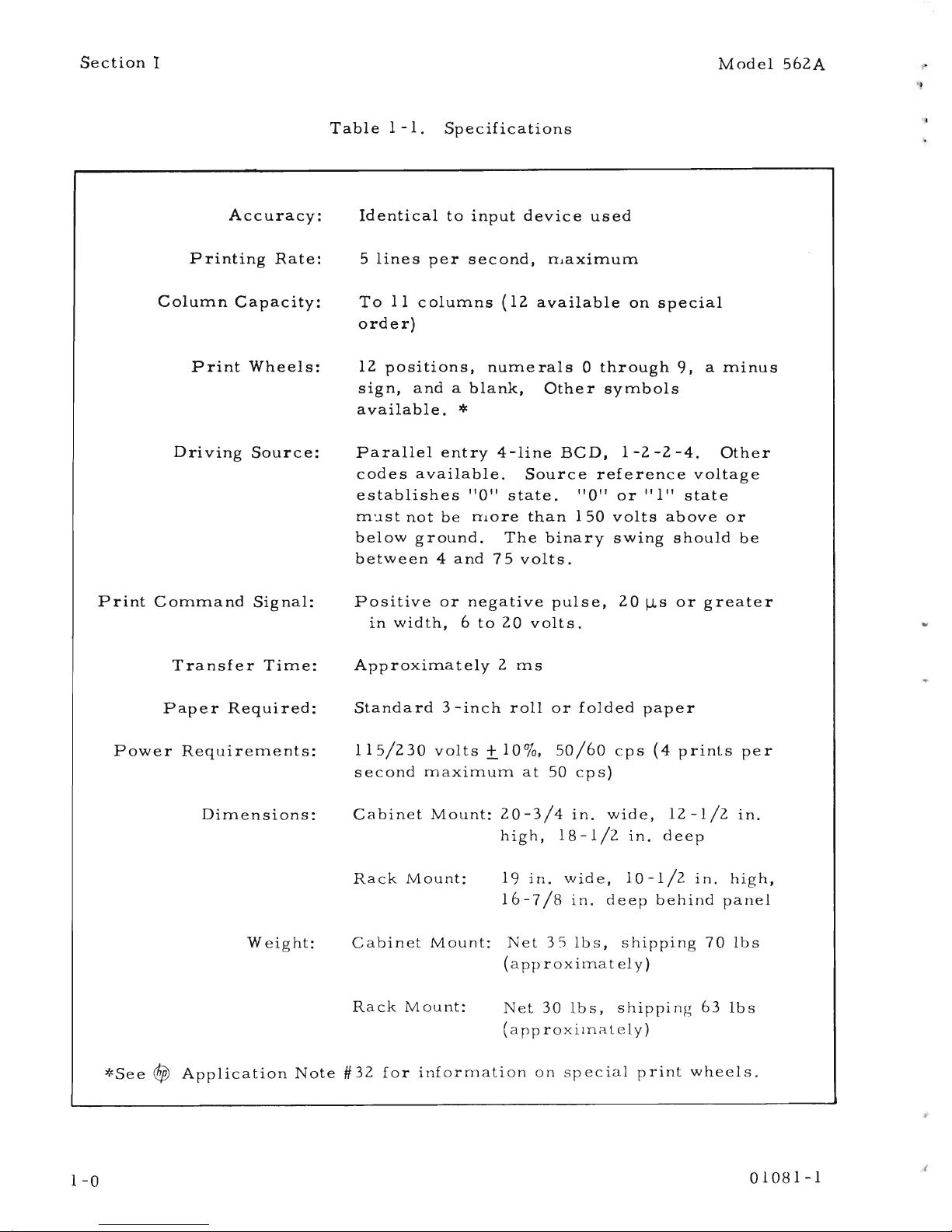
Table1-1.
Specifications
Accuracy:
Printing
Rate:
Column
Capacity:
Print
Wheels:
Dri
ving
Source:
Print
Command
Signal:
Transfer
Time:
Paper
Required:
Power
Requirements:
Dimensions:
Identical
to
input
device
used
5
lines
per
second,
nlaximum
To
11
columns
(12
available
on
special
order)
12
positions,
numerals
0
through
9,
a
minus
sign,
andablank,
Other
symbols
available.
*
Para11e1entry4-Ii
ne
BCD,
1 - 2 - 2 -
4.
at
her
codes
available.
Source
reference
voltage
establishes
"0"
state.
"0"
or
"1"
state
m'..lst
not
be
nlore
than
150
volts
above
or
below
ground.
The
binary
swing
should
be
between
4
and
75
volts.
Positive
or
negative
pulse,
20
\J.s
or
greater
in
width,
6
to
20
volts.
Approximately
2
rns
Standard
3
-inch
roll
or
folded
paper
115/230
volts
±
10%,
50/60
cps
(4
prints
per
second
maximum
at
50
cps)
Cabinet
Mount:
20-3/4
in.
wide,
12-1/2
in.
high,
18-1/2
in.
deep
Rack
Mount:
19
in.
wide,
10-1/2
in.
high,
16-7/8
in.
deep
behind
panel
Weight:
Cabinet
Mount:
Net
35
lbs,
shipping
70
lbs
(app
roximat
el
y)
Rack
Mount:
Net
30
Ibs,
shipping
63
lbs
(app
roxilna
LeI
y)
1-0
*
See
0j)
A ppIicat
ion
Not
e #32forinf
0 r
mat
ion
0 n s
pee
i a I p r i nt wh
eel
s .
01081-1
Page 6
Model
562A
1-1.
DESCRIPTION.
SECTION
I
GENERAL
DESCRIPTION
Section
I
The
Hewlett-Packard
Model
562A
Digital
Recorder
isatransistorized
electro-
IT!echanical
device
providing
a
printed
record
of
digital
inforrnation.
Parallel
data
entry
and
low-inertia
moving
parts
allow
printing
rates
as
high
as5lines
per
second,
each
line
containing
up
to
11
digits;
12
digit
capacity
is
available
on
special
order.
Throughout
this
nlanual
the
Model
562A
will
be
referred
to
as
the
recorder.
1-2.
DATA
ENTRY.
Standard
input
for
the
recorder
is
parallel-entry
4-line
BCD
code,
either
1224
or
1248.
Input
to
the
recorder
is
through
rear-l1'.lounted
connectors.
Internal
connectors
route
the
inforn1ation
to
any
desired
sequence
of
columns.
Each
column
has
binary
storage
for
one
decimal
nunlber.
When
a
print
COITlmand
is
supplied,
each
storage
unit
assumes
the
condition
of
the
decade
counting
unit
(or
other
driving
source)
connected
to
it.
The
data
transfer
takes
place
in
approximately
2
milliseconds,
after
which
tinle
the
d
riving
source
is
free
to
gather
more
infornlation.
1-3.STANDARD
INSTRUMENT.
Each
storage
unit
is
mounted
onaplug-in
board
(column
board)
withade-coding
matrix.
The
nlatrix
converts
the
stored
data
into
positioning
inforIT!ation
for
the
print
wheels.
The
recorder
is
supplied
to
translate
1224
BCD
codes,
but
other
4-line
codes
are
accoIYlmodated
by
substituting
plug-in
boards.
Unless
otherwise
specified,
the
recorder
is
supplied
from
the
factory
with
the
following:
a.
Six
+1224
coluIYln
boards.
b.
Printer
nlechanism,
11
print
wheels
and
associated
components,
five
prints/second
with
60
cps
power
line
frequency.
c.
One
input
connector
at
rear
of
recorder
JI01.
d.
One
input
cable.
e.
One
control
board.
f.
One
power
supply
board.
01081-1
1-1
Page 7
Section
I
1-4.
OPTIONS
AVAILABLE.
The
following
options
are
available:
a.
+
or
-1224
column
boards.
b.
+
or
-1248
column
boards.
c.
Analog
circuitry.
d.
Pinion
gear,
allows
5
prints
per
second
with
50
cps
power.
Model
562A
e.
Input
connector
(J201)
and
associated
connectors
(for
dual
input
operation
or
over9-column
capacity).
f.
Data
input
cable.
1-5.
POWER
REQUIREMENTS.
The
recorder
has
been
designed
to
operate
frorr!
115/230
volt,
50/60
cps
power.
A
switch,
located
at
the
rear
of
the
recorder
selects
operation
for
either
115
or
230
volts.
The
three-conductor
power
cable
supplied
with
the
instrument
is
terminated
in
a
three-prong
polarized
male
connector
recommended
by
the
Electrical
Manu-
facturers'
Association
(NEMA).
The
third
contact
is
an
offset
round
pin,
added
toastandard
two-blade
ac
plug
which
grounds
the
recorder
chassis
when
used
with
the
proper
receptacle.
An
adapter
should
be
used
to
connect
the
NEMA
plug
toastandard
two-contact
receptacle.
When
the
adapter
is
used,
the
ground
connector
becomes
a
short
green
lead.
The
green
lead
should
be
connected
to
a
suitable
ground
for
protection
of
the
operating
personnel.
1-6.
USES.
Because
of
the
extreme
flexibility
of
the
recorder,
it
can
be
used
with
electronic
counters,
digital
voltmeters
etc.
orawide
variety
of
individual
and
system
applications.
The
recorder
will
operate
with+or
-1224,
+
or
-1228
BCD,
and
10
-line
code
information
depending
on
column
boards
installed.
Two
separate
sources,
unsynchronized,
can
be
used
to
provide
data
if
option
e
is
installed.
The
recorder
supplies
the
synchronization.
When
the
analog
circuitry,
option
c,
is
installed,
the
operator
may
select
analog
voltage
of
columns
1
through
9
in
3
-column
groups.
1
-2
01081-1
Page 8
Model
562A
SECTION
II
INSTALLATION
2-1.
GENERAL
INFORMATION.
Section
II
Section
II
contains
information
relating
to
installation
and
input
connections.
2-2.
RACK
MOUNTING.
If
the
recorder
is
to
be
rack
mounted,
be
certain
to
allow
sufficient
open
space
for
cooling
air
to
enter
and
exhaust.
Do
not
rnount
the
recorder
next
to
equip-
ment
which
will
discharge
hot
air
into
the
recorder
air
intake.
2-3.
CONNECTION
TO
THE
$p
TRANSISTORIZED
COUNTERS.
The
recorder
may
be
directly
connected
to
the
~
transistorized
counters
by
means
of
the
input
cable
supplied
with
the
recorder.
The
transistorized
counters
have
the
correct
connector
installed.
Recorder
connector
J101
is
connected
to
the
counter
recorder
connector.
If
a
second
transistorized
counter
is
to
be
connected
to
the
recorder,
connection
is
made
froIn
the
second
counter
to
recorder
connector,
J201.
The
transistorized
counter
output
is
+1224
BCD.
2-4.
CONNECTION
TO
rfiJ
COUNTERS
AND
DIGITAL
VOLTMETER.
If
the
recorder
is
to
be
connected
to
the
above
tube
type
instruments
a
modifi-
cation
kit
can
be
installed.
The
kit
provides
a
+1224
BCD
output.
2-5.
OPERATION
FROM
TWO
DATA
SOURCES.
The
recorder
can
be
operated
fronl
two
data
sources,
synchronized
or
unsyn-
chronized,
by
connecting
the
data
inputs
to
connectors
J101
and
J201.
The
two
data
inputs
can
be
±1224
or
±1248
code.
The
appropriate
coluInn
boards
Inust
be
installed
in
the
proper
connectors
in
the
recorder.
2-6.
CABLE
FABRICATION.
Connection
of
the
recorder
to
data
sources
other
than
the
above
Inay
require
construction
ofacable
terminated
withaconnector
that
will
mate
with
the
recorder
connectors.
Use
small
gage
telephone-type
wire.
Number
26
gage
wire
meeting
MIL-B
-76A,
with
7
strands
#34
gage
wire,
tinned
after
stranding,
with
10
SoC
plastic
insulation
has
been
found
satisfactory.
Select
a
sy
stematic
color
code
for
wires
to
avoid
errors.
Use
care
in
soldering.
Repairing
faulty
connections
after
all
wires
are
soldered
is
very
difficult.
A
length
of#14
gage
wire
makes
an
excellent
soldering
tip
for
use
on
closely-spaced
connector
terrninals.
01081-1
2
-1/2-2
Page 9
Model
562A
SECTION
III
OPERATION
3-1.
OPERATING
CONTROLS.
The
operating
controls
consist
of
the
following:
POWER
ON,
supplies
power
to
the
recorder
when
in
the
ON
position.
Section
III
RECORD
ON,
allows
the
printer
mechanism
to
operate
when
in
the
ON
position.
When
the
switch
is
in
the
spring-loaded
position(down),
the
recorder
prints
at
maximum
rate.
The
middleposition
isastandby
position(allows
analog
to
be
taken).
SPACE
SELECTOR,
selects
the
number
of
spaces
between
readout
prints.
PAPER
ADVANCE,
manually
advances
paper.
ANALOG
CONTROLS,
(optional)
refer
to
text.
3-2.
PAPER
TAPE.
Special
~folded
tape
is
recommended
for
use
with
the
recorder.
High-quality
standard
3
-inch
rolled
adding
machine
type
may
also
be
used.
Folded
tape
permits
convenient
take
-up
in
the
paper
drawer
and
allows
easy
inspection
of
any
portion
of
the
type.
It
is
perforated
at
each
fold
to
allow
neat
separation
of
portions
of
recorded
data.
Folded
tape
may
be
reversed
and
re-
run
to
use
both
sides.
With
single
spacing,
about
15,
000
prints
can
be
made
on
one
side
ofafolded
pad.
One
pad
will
last
about
40
minutes
at
maximum
print
rate.
To
install
the
paper
tape
proceed
as
follows:
a.
Open
front
panel.
b.
Load
paper
in
compartment.
c.
Fold
paper
back
one
inch
and
crease.
Insert
paper
between
roller
and
guide
plate.
01081-1
3-1
Page 10

Section
III
Model
562A
d.
Manually
advance
paper.
Paper
will
feed
easier
and
can
be
reversed
with
SPACE
SELECTOR
set
to
"0".
e.
Feed
paper
under
inked
ribbon.
f.
Feed
paper
through
slot.
Close
front
panel.
g.
Collect
printed
paper
in
drawer.
Follow
these
additional
instructions
if
roll
tape
is
used:
a.
Insert
spindle
through
roll.
Spindle
is
taped
to
bottom
of
paper
compart-
ment
when
instrument
is
shipped
from
the
factory.
b.
Hang
roll
by
ends
of
spindle
from
ledges
on
both
sides
of
paper
compartment.
c.
Paper
must
feed
out
from
the
bottom
of
the
roll.
d.
Continue
with
loading.
To
feed
paper
rapidly
use
the
PAPER
ADVANCE
thumb
wheel.
To
manually
feed
paper
backward,
set
the
SPACE
SELECTOR
to
"0"
and
roll
the
PAPER
ADVANCE
wheel
in
the
reverse
(up)
direction.
Paper
feed
may
be
reversed
on!l.
with
the
SPACE
SELECTOR
set
to
"0".
Be
sure
paper
is
inserted
squarely
in
the
paper
feed
mechanism
to
prevent
jamming.
If
paper
doesnot
feed
smoothly,
place
the
RE
CORD
switch
in
the
centerposition,
and
re
move
all
paper
from
the
feed
mechanism.
Use
tweezers
to
pick
out
torn
bits
of
paper.
3-3.
INKED
RIBBON.
The
printer
mechanism
uses
a
special
heavily-inked
silk
ribbon
available
from
the
Hewlett-Packard
Company.
Standard
typewriter
ribbon
on
an
Underwood
spool,
with
reversing
rivets
near
the
ribbon
ends,
may
also
be
used;
however,
impressions
will
be
lighter
than
with
the
Hewlett-Packard
ribbon.
To
install
new
ribbon,
proceed
as
follows:
a.
Open
the
hinged
front
panel
to
gain
access
to
the
printer
mechanism.
b.
Loosen
the
two
printer
mechanism
retaining
screws
located
on
the
lower
front
corners
of
the
mechanism
by
turning
1/4
turn
counterclockwise.
c..Slide
mechanism
out
of
cabinet
until
ribbon
spools
are
readily
accessible.
d.
Wind
all
the
ribbon
onto
one
spool.
3-2
01081-1
Page 11

Model
562A
Section
III
01081-1
e.
Shift
the
two
ribbon
spool
retaining
springs
away
from
the
spools,
and
remove
spools.
f.
Take
the
ribbon
out
of
the
mechanism.
Save
the
empty
spool.
g.
Hook
end
of
new
ribbon
on
empty
spool.
Wind
about
10
inches
of
ribbon
on
the
spool
so
that
the
rever
sing
rivet
is
on
the
spool.
h.
Install
new
ribbon
by
feeding
it
over
the
ribbon
rollers
and
between
the
print
wheels
and
paper
tape.
i.
Feed
ribbon
through
the
slots
in
the
reversing
arms
and
around
the
lower
guides.
Ribbon
must
be
twisted
900between
the
ribbon
roller
and
the
slot
in
the
rever
sing
arm.
j.
Place
ribbon
spools
on
their
shafts.
Fasten
spools
in
place
with
the
spool
retaining
springs.
Ribbon
must
feed
out
from
the
bottom
of
each
spool.
k.
Replace
printer
mechanism
in
cabinet
and
tighten
retaining
screws.
3-4.
TAPE
DUPLICATES.
Transparent
paper,
~stock
no.
9251-0052
is
recommended
for
use
in
the
recorder.
This
paper
produces
much
less
paper
dust
and
copies
can
be
easily
made
with
duplication
machines.
If
duplicate
tape
records
are
required
from
standard
paper,
contact
print
duplicating
methods,
such
as
the
ozalid
process,
can
be
used
by
printing
directly
from
the
original
tape
records.
3-5.
PROGRAMMING
THE
RECORDER.
The
recorder
can
be
programmed
to
accept
different
codes
if
the
proper
column
boards
are
installed.
The
column
boards
may
be
inter-mixed
if
desired.
The
standard
recorder
is
supplied
with
six
+1224
BCD
column
boards,
with
connectors
installed
to
accept
a
total
of
nine
column
boards.
If
more
than
nine
column
operation
is
desired,
J201
must
be
installed
with
the
connectors
that
attach
to
the
rear
of
the
column
boards
(PIIO-PIl5).
Normally
JIOl
supplies
data
to
column
boards
Al-A9,
but
connectors
PIOl-
PI09
can
be
connected
to
supply
data
to
any
of
the
column
boards
the
operator
desires.
J201
can
supply
data
to
any
of
the
remaining
column
boards.
Con-
nectors
PIIO-Pll5
can
be
connected
to
supply
data
to
six
column
boards.
3-6.
PROGRAMMING
THE
CONTROL
BOARD
(AI3).
Connectors
P20l
and
P202
supply
control
signals
to
the
data
sources,
and
return
data
source
signals
to
the
control
board.
Connector
P20l
is
con-
3-3
Page 12
Section
III
Model
562A
nected
to
one
data
source
through
JI01.
and
P202
toasecond
data
source
through
J201.
The
control
board
senses
when
commands
from
both
sources
have
been
received,
then
starts
the
printing
cycle.
If
only
'one
data
source
is
used,
the
control
board
connector
that
is
not
being
used
must
be
disconnected,
otherwise
the
recorder
will
not
operate
but
will
wait
until
the
control
boarq
receives
a
second
print
command
signal.
When
the
control
board
connector
that
is
not
being
used
is
disconnected,
the
associated
print
command
binary
remains
in
the
proper
state
of
unbalance.
Thus
a
print
command
is
required
from
only
one
data
source
to
start
the
printing
cycle.
3-7.
DATA
SOURCE
CONNECTIONS.
Data
can
be
supplied
continuously
from
two
data
sources.
If
six
column
read-
out
is
desired
for
one
data
source
and
five
column
readout
is
desired
for
the
second
data
source,
then
one
data
source
is
connected
to
JI01
and
the
other
data
source
to
J201.
The
column
board
connectors
can
be
connected
as
the
operator
desires.
Other
combinations
the
operator
may
want
can
be
had
by
changing
the
connectors
at
the
rear
of
the
column
boards.
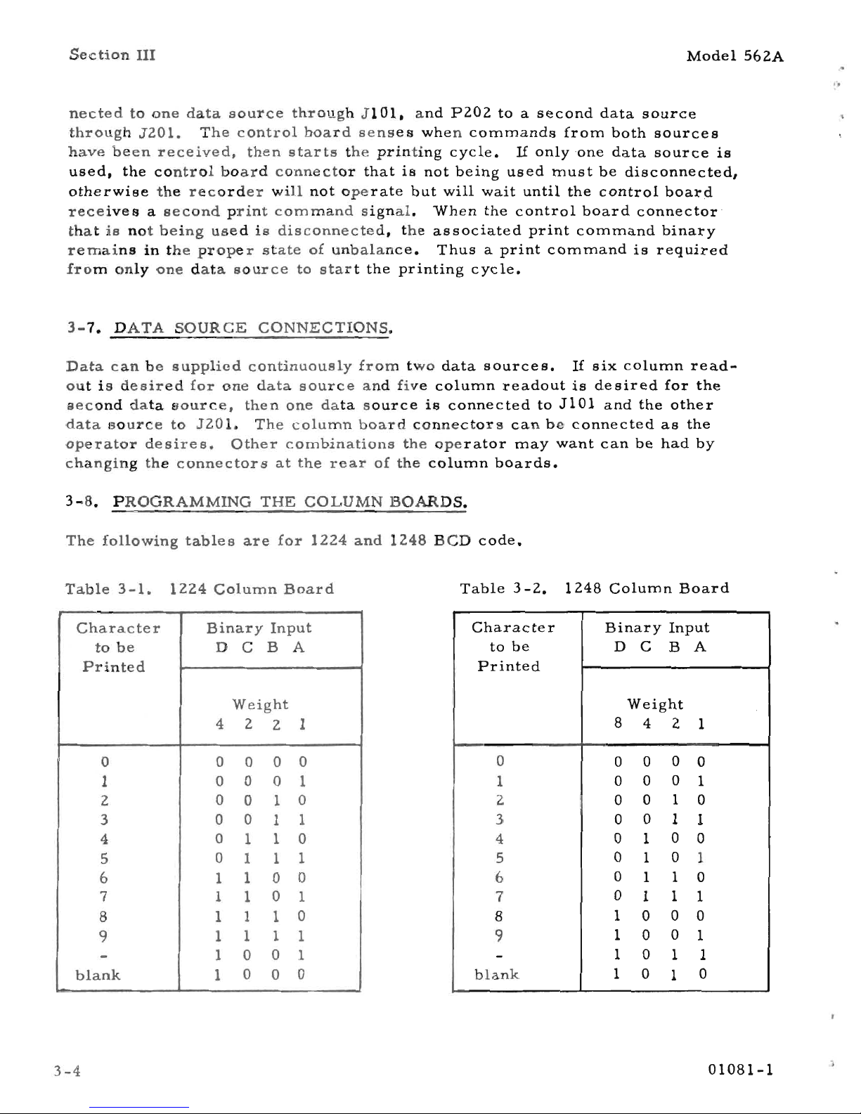
3-8.
PROGRAMMING
THE
COLUMN
BOARDS.
The
following
tables
are
for
1224
and
1248
BCD
code.
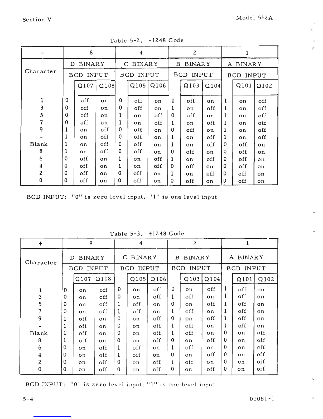
Table3-1.
1224
Column
Board
Character
Binary
Input
to
be
D C
B
A
Printed
Weight
4 2
2
1
0 0 0
0
0
1
0
0
0
1
2
0
0
1
0
3
0 0
1
1
4
0
1
1
0
5
0
1 1 1
6 1 1
0 0
7
1
1
0 1
8 1 1 1
0
9
1
1
1 1
-
1
0 0
1
blank
1
0 0
0
3-4
Table3-2.
1248
Column
Board
Character
Binary
Input
to
be
D
C B
A
Printed
Weight
8
4
2
1
0
0 0
0
0
1
0 0 0
1
2 0 0 1
0
3
0
0
1
1
4
0
1
0 0
5
0
1
0
1
6
0
1
1
0
7
0
1
1
1
8 1
0 0
0
9
1
0 0
1
-
1
0
1
1
blank
1
0
1
0
01081-1
Page 13
Model
562A
The
following
notes
refer
to
tables3-1
and3-2:
1
and0definitions
1)
1
indicates
"1"
level
binary
input.
2)
0
indicates
"0"
level
binary
input.
Section
III
"1"
and
"0"
levels
(BCD
input)
1)
Ina+1224
code,
the"
1"
level
is
positive
with
respect
to
the
"0"
level.
2)
Ina-1224
code,
the"
1"
level
is
negative
with
respect
to
the
"0"
level.
The
+
or
-
prefix
is
deterrnined
by
the
polarity
of
the"
1"
level
with
respect
to
the
"0"
level.
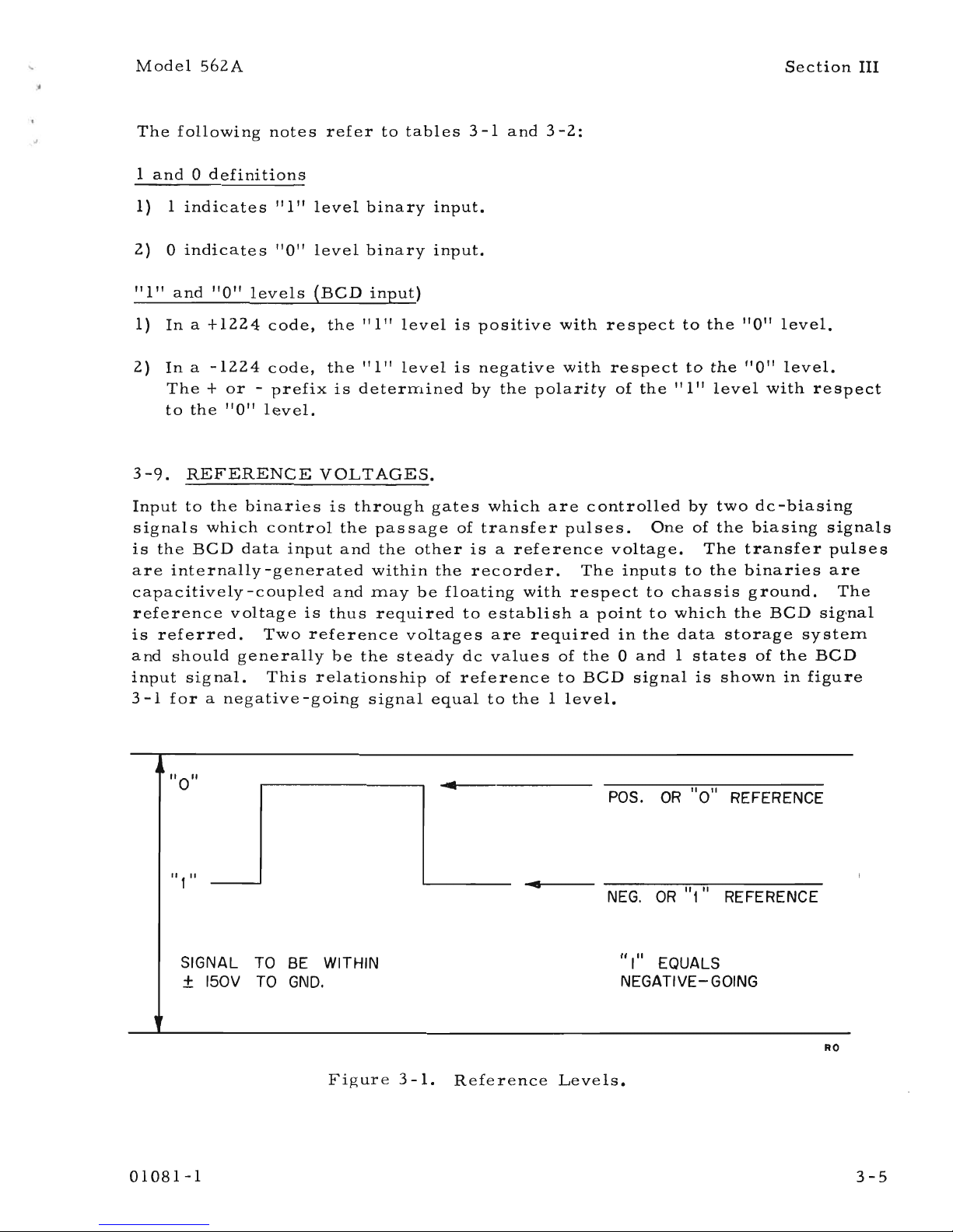
3-9.
REFERENCE
VOLTAGES.
Input
to
the
binaries
is
through
gates
which
are
controlled
by
two
dc
-biasing
signals
which
control
the
passage
of
transfer
pulses.
One
of
the
biasing
signals
is
the
BCD
data
input
and
the
other
is
a
reference
voltage.
The
transfer
pulses
are
internally-generated
within
the
recorder.
The
inputs
to
the
binaries
are
capacitively-coupled
and
may
be
floating
with
respect
to
chassis
ground.
The
reference
voltage
is
thus
required
to
establish
a
point
to
which
the
BCD
sig'nal
is
referred.
Two
reference
voltages
are
required
in
the
data
storage
system
and
should
generally
be
the
steady
dc
values
of
the0and1states
of
the
BCD
input
signal.
This
relationship
of
reference
to
BCD
signal
is
shown
in
figure
3-1
for
a
negative-going
signal
equal
to
the1level.
"0"
"1"
SIGNAL
TO
BE
WITHIN
±
150V
TO
GND.
POS.
OR
"0"
REFERENCE
NEG.
OR"
1" REFERENCE
It
I"
EQUALS
NEGATIVE-GOING
RO
Figure
3
-1.
Reference
Levels.
01081-1
3-5
Page 14
Section
III
3-10.
REFERENCE
VOLTAGE
ADJUSTMENT.
Model
562A
The
input
voltage
applied
for
any
column
board
must
not
exceed
150
volts.
That
is
the
refe
renee
voltage
plus
theBCD
It1It
level
should
not
be
greater
than
150
volts.
For
instance,
if
the
BCD
swing
is
from
100
volts
(tiD"
level)
to
160
volts
(til"
level)
then
attenuation
must
be
introduced
to
reduce
the
"0"
level
to
94
volts
and
the
"1"
level
to
150
volts.
The
minus
reference
voltage
can
then
be
adjusted
for
94
volts.
The
plus
reference
level
must
then
be
adjusted
to
150
volts.
Before
a
reference
voltage
can
be
chosen,
the
"0"
and"
I"
levels
of
the
equip-
ment
supplying
the
BCD
signals
must
be
known.
For
instance
if
the
recorder
is
connected
toabinary
counter
with
a
-1248
code,
each
column
board
will
be
driven
byadecade
in
the
counter.
Sometimes
binaries
in
the
decades
have
different"
1"
and"
0"
levels,
thus
a
proper
reference
voltage
must
be
chosen.
If
the
column
board
is
a
-1248
code,
then
the
-reference
voltage
must
be
chosen
that
includes
the
"1"
levels
applied
to
the
A,
B,
C,
and
D
binaries.
A
+reference
voltage
must
be
chosen
that
will
include
the
"0"
levels
for
the
A,
B,
C,
and
D
binaries.
If
high
impedance
reference
levels
are
used
(above
5000
ohms),
suitable
by-
passing,
providing
a
time
constant
of
150
~s,
should
be
used.
If
the
BCD
drive
is
derived
from
an
unregulated
supply,
then
it
is
desirable
to
obtain
the
reference
voltage
from
the
same
unregulated
supply.
3-11.
POWER
SUPPLY
AND
INTERNAL
REFERENCE
VOLTAGES.
The
power
supply
board,
A16,
supplies
the
de
voltages
required
by
the
recorder.
The
power
supply
also
has
provisions
for
providing
reference
voltages
of
-9
to
+17
volts.
The
operator
can
select
a
value
of
resistors
or
breakdown
diodes
needed
to
provide
the
proper
reference
voltages.
Connectors
P301
and
P302
(optional)
supply
the
reference
voltages
to
the
column
boards.
When
using
an
external
reference
voltage,
connectors
P30l
and
P302
must
be
disconnected
from
the
power
supply
board
if
resistors
are
installed.
Unless
specified
by
the
customer,
resistors
are
not
installed.
The
proper
mounting
holes
are
in
the
power
supply
board
and
the
operator
can
install
the
resistors
or
break-
down
diodes
required
to
give
the
desired
voltage.
3
-12.
PRINTING
A
MINUS(-).
The
recorder
will
normally
print
a
blank
with
no
BCD
input.
If
the
operator
wishes
to
print
a
-(minus)
for
a
1224
code,
in
place
ofablank,
proceed
as
follows:
In
table
3-1
under
the
column
headed
"character
to
be
printed",
find
-(minus).
Under
the
"Binary
Input"
column,
the-charac
ter
must
have
a
"l"
input
for
the
A
and
D
binaries.
If
the
column
board
isa+1224
code,
then
the
external
voltage
applied
to
the
A
binary
input
must
be
at
least
4
volts
more
positive
than
the
negative
reference
voltage.
Since
the
D
binary
has
a
11
I"
supplied
3-6
01081-1
Page 15
Model
562A
Section
III
01081-1
by
the
transfer
pulse
when
the
nOll
level
is
not
present,
no
external
voltage
is
required
for
the
D
binary.
A
-1224
code
req
uiresthe
same
voltagesbut
of
different
polarity.
If
the
column
board
isa+1248
code,
in
table
3-2
find
-(minus).
Under
the
"Binary
Input"
column,
the-character
must
have
a
"l"
input
for
the
A,
B,
and
D
binaries.
An
external
voltage
applied
to
the
A
binary
must
be
at
least
4
volts
more
positive
than
the
negative
reference
voltage.
The
Band
D
binaries
do
not
require
an
external
voltage
as
the
transfer
pulse
supplies
the"
1"
level
when
"0"
level
is
not
present.
A
-1248
code
requires
the
same
external
voltages,
but
of
different
polarity.
3-13.
SETTING
THE
ANALOG
CONTROLS
(ortional).
The
POTENTIOMETER
RECORDER
binding
posts
on
the
562A
are
designed
to
operate
potentiometer
type
(voltage
operated)
recorders
having
lOO-millivolt-
full-scale
sensitivity,
and
greater
than
50K
ohm
input
resistance.
The
562A
can
also
drive
recorders
having
other
values
of
input
sensitivity
and
resistance
by
making
minor
addiqons
or
modification
to
the
POTENTIOMETER
RE-
CORDER
ANALOG
OUTPUT.
To
use
the
562A
onapotentiometer
recorder,
proceed
as
follows:
a.
Set
the
COLUMN
SELECTOR
to
include
the
three
number
columns
to
be
recorded
gr
aphically.
b.
Connect
the
potentiometer
recorder
to
the
POTENTIOMETER
RECORDER
binding
postson
the
56
2A.
c.
Set
the
OPERATE
lever
switch
to
the
G8.LV.
ZERO
position
(the
GALV.
ZERO
control
has
no
effect
on
the
POTENTIOMETER
RECORDER
output)
but
does
supply
zero
output
at
potentiometer
jack.
d.
Zero
set
the
potentiometer
recorder
with
its
own
controls.
e.
Set
the
OPERATE
lever
switch
to
the
CALIBRATE
position.
f.
Adjust
the
CALIBRATE
control
to
obtain
full-scale
deflection
of
the
recorder
pen.
g.
Repeat
steps
c,
d,
e,
and
f.
h.
Set
the
OPERATE
lever
switch
to
OPERATE.
The
graphic
recorder
will
now
plot
the
number
columns
indicated
by
the
COLUMN
SELECTOR.
3-14.
RECORDING
WITH
GALVANOMETER
GRAPHIC
RECORDERS.
The
GALVANOMETER
RECORDER
output
jack
on
the
562A
is
designed
to
operate
galvanometer
type
(current
operated)
recorders
having
I-milliampere-
3-7
Page 16

Section
III
Model
562A
3-8
full-scale
se
nsitivity
and
Ie
s s
than
5000
ohnlS
input
re
sis
tance.
The
562A
can
also
drive
recorders
having
other
values
of
input
sensitivity
and
resistance
by
making
minor
additions
or
modifications
to
the
GALVANOMETER
RECORDER
ANALOG
OUTPUT.
To
use
the
562A
withagalvanometer
recorder,
proceed
as
follows:
a.
Before
connecting
the
recorder
to
the
562A,
deternline
which
three
of
the
number
columns
are
to
be
plotted.
Then
set
the
COLUMN
SELECTOR
to
in-
clude
these
three
number
columns.
b.
Zero
set
the
galvanometer
recorder
with
its
own
controls.
c.
Connect
the
recorder
to
the
GALVANOMETER
RECORDER
jack
using
a
standard,
1/4-inch
diameter
three-circuit
phone
plug.
The
positive
recorder
terminal
is
connected
to
the
ring
contact
on
the
plug,
and
the
negative
terminal
to
the
tip
on
the
plug.
d.
Set
the
OPERATE
lever
switch
to
the
GALV.
ZERO
position.
e.
If
necessary,
zero
set
the
recorder
with
the
GALV.
ZERO
set
control
on
the
562A.
f.
Set
the
OPERATE
lever
switch
to
the
CALIBRATE
position.
g.
Adjust
the
CALIBRA
TE
control
to
obtain
full-scale
deflection
of
the
recorder
pen.
h.
Set
the
OPERATE
lever
switch
to
the
OPERATE
position.
The
recorder
will
now
plot
the
number
columns
indicated
by
the
COLUMN
SELECTOR.
3-15.
USING
GRAPHIC
RECORDERS
HAVING
DIFFERENT
INPUT
SENSITIVITIES.
To
use
a
potentiometer
recorder
having
greater
than
specified
voltage
sensi-
tivity,
shunt
the
recorder
with
a
value
of
resistance
which
results
in
full-scale
deflection
of
the
recorder
pen
while
the
562A
is
set
to
CALIBRATE
and
the
CALIBRATE
control
is
cente
red.
Potentiometer
recorders
having
less
than
50K
ohm
input
resistance
may
be
used,
but
the
POTENTIOMETER
RECORDER
output
will
than
provide
less
than
100
millivolts
for
full-scale
deflection.
The
internal
resistance
at
the
POTENTIOMETER
RECORDER
output
is
approximately
2500
ohms
and
when
loaded
with
this
value,
provides
only
50
millivolts
for
full
scale
deflection.
If
the
potentiometer
recorder
has
sufficient
sensitivity
to
operate
with
the
lower
input
level,
no
modification
is
required
to
use
the
recorder.
However,
as
the
external
resistance
on
the
POTENTIOMETER
RECORDER
binding
posts
is
decreased,
so
is
the
range
of
the
CALIBRATE
control,
until
at
sonle
low
resistance
it
may
be
necessary
to
provide
an
external
calibrating
control
01081-1
Page 17

Model
562A
Section
III
01081-1
consisting
ofapotentiometer
connected
asavariable
shunt
for
the
signal
which
is
fed
to
the
graphic
recorder.
If
a
potentiometer
or
galvanometer
recorder
is
to
be
used
which
requires
slightly
greater
output
voltage
or
current,
it
is
possible
to
increase
the
562A
ANALOG
OUTPUT
by
changing
the
values
of
certain
resistors
in
the
analog
circ
ufts.
3-9/3-10
Page 18
Model
562A
SECTION
IV
THEOR
Y
OF
OPERATION
4-1.
INTRODUCTION.
Section
IV
Operation
of
the
562A
is
dependent
uponaseries
of
timing
and
reference
volt-
ages.
The
timing
voltages
are
supplied
by
the
control
board
(Al3).
Reference
voltages
can
be
supplied
by
the
power
supply
(A14)
or
by
an
external
source.
The
following
paragraphs
will
describe
the
functions
of
various
circuits
in
the
recorder.
4-2.
CONTROL
BOARD
OPERATION.
Operation
of
the
recorder
is
dependent
upon
a
series
of
timing
voltages
developed
by
the
control
board.
Refer
to
the
functional
diagram,
figure
5-2.
Assume
the
data
source
initiates
a
print
command.
Print
Command
Binary
Number
1
changes
state
and
immediately
supplies
the
data
source
withadisable
voltage.
Assume
Print
Command
Binary
Number
2
has
its
input
connector
arranged
so
only
one
print
is
required.
The
Print
Scan
Schmitt
is
in
the
proper
state
because
the
shutter
is
open.
The
Print
Scan
Schmitt
applies
the
proper
signal
to
the
"And"
Gate.
The
"And"
Gate
conducts
and
causes
the
Clutch
Binary
to
change
state.
The
clutch
solenoid
starts
to
energize.
When
the
Clutch
Binary
changes
state,
a
signal
is
applied
to
the
Delay
Multivi-
brator
(2MS).
The
output
of
the2ms
delay
multivibrator
produces
a
reset
pulse
which
is
applied
to
the
storage
binaries.
This
removes
stored
information
and
sets
the
storage
binaries
in
the
proper
state
to
receive
new
information.
The
output
of
the2ms
delay
multivibrator
is
also
applied
toa60
J-Ls
delay
multi-
vibrator.
The
output
of
the
60
J-LS
multivibrator
is
applied
to
the
storage
binary
gate
diodes
by
way
of
the+and-Transfer
Amplifiers,
then
data
transfer
takes
place.
The
output
of
the
60
f.LS
multivibrator
is
also
applied
to
the
Print
Command
Binaries
and
resets
them.
While
this
action
is
occurring,
the
clutch
solenoid
is
completing
its
pull-in
cycle.
When
the
clutch
solenoid
has
engaged
the
clutch,
the
clutch
will
remain
engaged
for
one
complete
revolution
of
the
clutch
assembly
because
of
mechanical
action.
As
the
clutch
assembly
rotates,
the
shutter
closes,
de-energizing
the
photo
conductor.
This
causes
the
schmitt
to
change
state,
initiating
the
scan
signal.
The
scan
signal
then
resets
the
clutch
binary
and
opens
the
Inhibit
Gate
circuits
which
can
allow
the
pawl
magnets
to
energize.
When
the
brush
senses
the
correct
voltage,
the
pawl
magnets
de
-energize
and
lock
the
print
wheels
at
the
proper
position.
Then
the
character
is
printed
as
the
clutch
assembly
finishes
its
one
revolution,
disengages,
and
opens
the
shutter.
The
photo
conductor
is
energized
and
the
system
is
ready
for
the
next
print
command.
01081-1
4-1
Page 19
Section
IV
4-3.
GOLUMN
BOARD
OPERATION.
Model
S62A
4-2
The
following
theory
is
for
operation
ofa-1248
code
column
board.
Assume
a
data
source
has
initiated
a
print
command,
the
AND
GATE
in
the
control
board
conducts,
and
the
clutch
solenoid
starts
to
energize.
A
signal
is
then
applied
to
the
2
MS
DELA
Y
lY1ULTIVIBRA
TOR
by
the
clutch
binary.
After
2
ms,
the
nlultivibrator
applies
a
positive
reset
pulse
to
the
column
boards.
The
binaries
reset
as
follows:
A
BINARY:
Q
101,
on;
0102,
off
B
BINARY:
a 1
03,
off;
0104,
on
G
BINAR
Y:
a
105,
on;
a
106,
off
D
BINARY:
Q
107,
off;
a
108,
on
The
data
source
is
supplying
bcd
information
to
the
four
binarie
s.
Suppose
the
bcd
information
supplied
is
for
the
decimal
number
8.
According
to
table
3-1,
"0"
level
information
will
be
supplied
to
the
G,
B,
and
A
binaries.
The
D
binary
will
have
"l"
level
information
supplied.
The
"0"
or
"l'"
do
not
change
the
state
of
the
binaries.
The
-
and+transfer
pulses
cause
the
binaries
to
change
state
if
the
1t0"
orIIlit
levels
needed
are
present.
At
the
D
binary,
if
the
"1"
level
is
pre
sent
GR104
is
forward
biased
and
-
transfer
pulse
will
go
through
diode
gate
GR104.
Since
a
107
is
off,
the
D
binary
will
change
state,
a107
on
and
a108
off.
The
G
binary
has
"0"
level
information
applied
to
diode
gate
GRI03.
A +
trans-
fer
pulse
is
applied
to
GRI03.
Since
the
"a"
level
information
applied
to
GRI03
is
equal
to
the
+
reference
voltage,
the
diode
will
pass
the+transfer
pulse.
Thus
QIOS
is
off
and
al06
is
on.
The
B
binary
has"
0"
level
information
applied
to
diode
gate
GR102.
Since
the
"Olt
level
information
is
(at
least
4
volts)
more
positive
than
the
-reference
voltage,
diode
GRl02
is
reverse
biased
and
will
not
pass
the-transfer
pulse.
The
binary
will
not
change
state.
Transis
tora103
re
mains
off
anda104
re
nlains
on.
The
A
binary
has
"a"
level
information
applied
to
diode
gate
GRIOI.
The
"0"
level
mllst
be
equal
to
the
positive
reference
voltage.
This
causes
GRlOI
to
be
forward
biased
and
pass
the+transfp.r
pulse.
The
A
binary
changes
state,
QIOI
off
and
QI02
on.
Three
of
the
halves
of
the
binaries
that
are
"on"
will
return,
through
matrix
resistors,
to
pin
11
of
connectors
XAl-l
to
XA12
-1.
This
is
the
line
which
corresponds
to
the
decimal
number
8.
In
this
case,
R161,
R175,
and
Rl99
return
to
the
line
for
the
decimal
number
8.
These
resistors
make
the
line
for
the
number
8
go
to
app
roximatel
y +
15
volts.
Diode
gateGRl
a5
andGRl
Oh
sense
when
the
line
gets
to
approximately
+15
volts
and
cause
amplifiers
al09»
a
110,
and
Q
III
to
de
-energize
the
pawl
magnet.
The
pawl
then
locks
the
01081-1
Page 20

Model
S62A
Section
IV
print
wheel
at
that
position.
The
number
is
then
printed.
When
the
data
source
initiates
another
print
command,
the
scan
signal
occurs
a
short
time
later
and
causes
amplifiers
0109,0110,
and
0111
to
energize
the
pawl
magnet
if
the
data
input
has
changed.
The
print
wheel
rotates.
The
magnet
remains
energized
until
diode
CRI0S
has
+lS
volts
applied
from
the
matrix.
4-4.
ANALOG
CIRCUITRY
OPERATION.
Sincethe
column
boardscontain
stored
binary
information,
an
analog
function
can
be
derived
to
drive
a
strip
chart
recorder.
The
analog
circuitry
provides
the
following:
a.
A
graphic
presentation
whereby
the
trend
of
recorded
data
can
be
seen
at
a
glance.
b.
Three
digits
of
analog
information
where
full
scale
on
the
recorder
may
beafew
parts
per
million
of
the
original
printed
reading.
c.
A
recording
where
an
increasing
numerical
count
is
always
an
upward
direction
on
the
strip
chart
recording.
d.
An
analog
recording
which
is
always
on
scale.
To
derive
the
analog
voltage
a
switching
arrrangement
is
used
which
utilIzes
the
stored
binary
data
from
three
consecutive
columns
of
the
printed
data.
Any
three
of
the
first
nine
columns
may
be
used
as
well
as
the
first
two
right
hand
digits.
The
binary
output
data
is
weighted
according
to
the
code
required
by
the
storage
units.
Four
resistors
are
used
to
develop
a
staircase
function
from
the
four
storage
binaries.
The
four
weighting
resistors
are
in
the
ratio
4221.
Refer
to
the
analog
circuitry
schematic.
Each
of
the
three
storage
decades
then
produces
a
staircase
function
withalevel
proportional
to
the
numerical
value
of
its
stored
binary
data.
The
three
staircase
voltages
are
then
mixed
in
proportion
to
their
decade
value
or
in
the
ratio
of
1,
10,
100,
to
produce
a
single
staircase
function
1000
part
in
amplitude.
Each
discrete
step
then
represents.
10/0
of
full
scale
and
for
practical
purposes
is
an
analog
function.
This
output
voltage
is
then
attenuated
and
applied
directly
toapotentiometer
type
strip
chart
recorder.
The
analog
signal
is
also
applied
to
an
amplifier
whose
output
can
be
used
to
drive
a 1
rna
type
galvanometer
recorder.
Diode
clamps
insure
accurate
voltage
levels
before
mIXIng.
Compensation
elements
maintain
constant
output
over
wide
temperature
extremes.
01081
-1
4-3/4-4
Page 21
Model
562A
5-1.
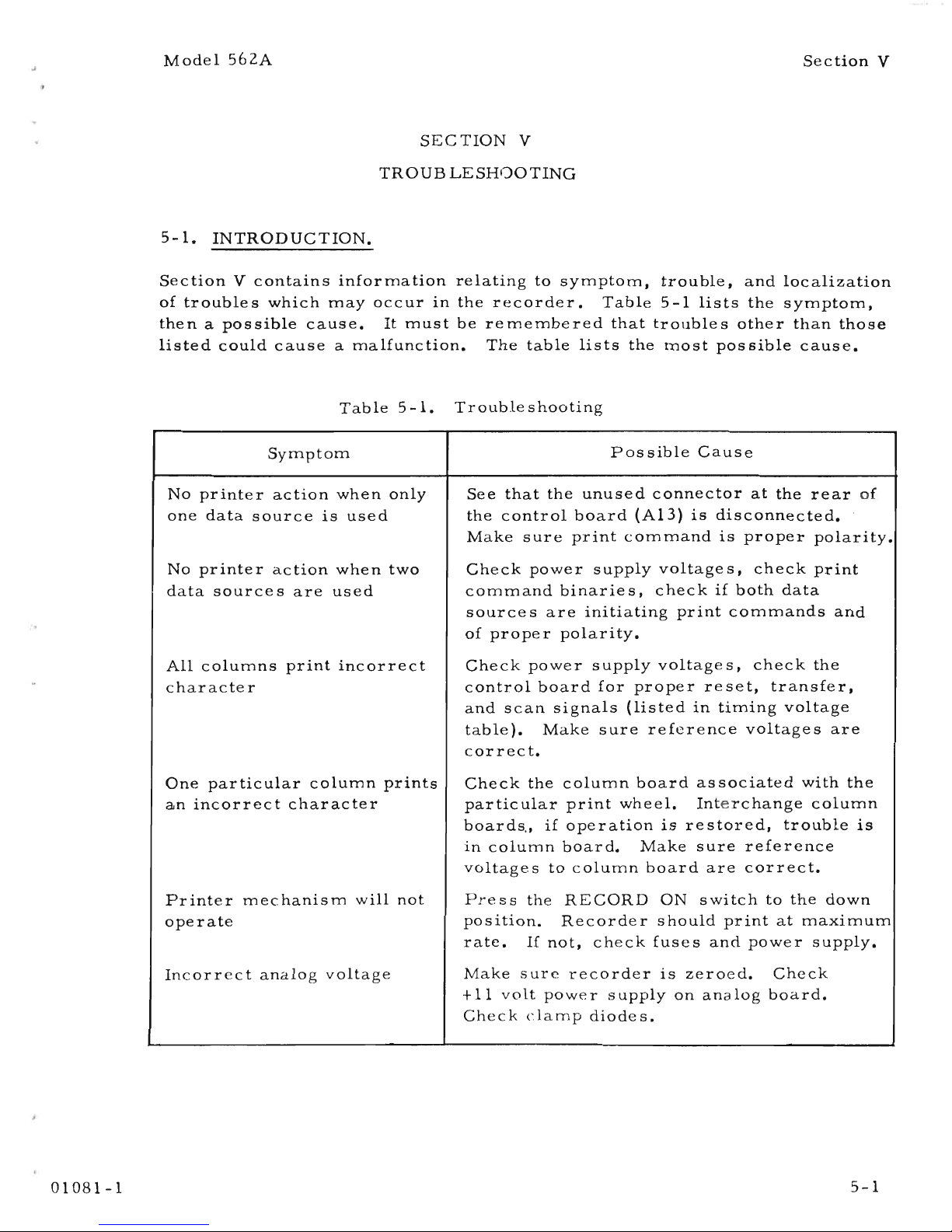
INTRODUCTION.
SECTION
V
TROUBLESHOOTING
Section
V
Section
V
contains
information
relating
to
symptom,
trouble,
and
localization
of
troubles
which
may
occur
in
the
recorder.
Table
5-1
lists
the
symptom,
then
a
possible
cause.
It
must
be
remembered
that
troubles
other
than
those
listed
could
cause
a
malfunction.
The
table
lists
the
most
possible
cause.
01081-1
Table
5-1.
Symptom
No
printer
action
when
only
one
data
source
is
used
No
printer
action
when
two
data
sources
are
used
All
columns
print
incorrect
character
One
particular
column
prints
an
incorrect
character
Printer
mechanism
will
not
operate
Incorrect
analog
voltage
Trouble
shooting
Possible
Cause
See
that
the
unused
connector
at
the
rear
of
the
control
board
(AI3)
is
disconnected.
Make
sure
print
command
is
proper
polarity.
Check
power
supply
voltages,
check
print
command
binarie
s,
check
if
both
data
sources
are
initiating
print
commands
and
of
proper
polarity.
Check
power
supply
voltages,
check
the
control
board
for
proper
reset,
transfer,
and
scan
signals
(listed
in
timing
voltage
table).
Make
sure
reference
voltages
are
correct.
Check
the
column
board
as
sociated
with
the
particular
print
wheel.
Interchange
column
boards"
if
operation
is
restored,
trouble
is
in
column
board.
Make
sure
reference
voltages
to
column
board
are
correct.
Press
the
RECORD
ON
switch
to
the
down
position.
Recorder
should
print
at
maximum
rate.
1£
not,
check
fuses
and
power
supply.
Make
sure
recorder
is
zeroed.
Check
tIl
volt
power
supply
on
analog
board.
Check
clamp
diodes.
5-1
Page 22
Section
V
5-2.
LOCALIZING
THE
TROUBLE.
Model
562A
5-2
Whenatrouble
has
been
traced
toaspecific
board,
make
voltagp.
meas
ure-
ments
on
base,
emitter,
and
collector
of
transistors.
On
the
column
board
binaries,
transistors
that
are
"turned
on"
will
have
approximately
t15
volts
on
the
collector,
transistors
that
are
"turned
off"
will
have
approximately
-5
volts
on
the
collectors.
Binary
tables
5-2
to
5-5
list
the
states
of
the
column
board
binary
transistors
for
various
numbers
and
inputs.
Binaries
in
the
control
board
can
be
checked
for
switching
action
withadc
coupled
oscillo-
scope.
Whenabinary
changes
state,
the
dc
coupled
oscilloscope
will
show
a
definite
change
of
dc
level.
A
vac
uum
tube
voltme
ter
can
be
used
also.
Figure
5-1
shows
the
timing
voltages
and
sequence.
Resistance
measurements
made
between
various
sockets
and
connectors
may
be
helpful.
For
this,
use
the
wiring
and
power
supply
diagram.
5-3.
SEMI-CONDUCTOR
REPLACEMENT.
Table
5-3
lists
the
various
transistors
and
diodes.
When
a
commercial
replacement
type
is
not
listed,
the
semi-conductor
should
be
ordered
from
the
Hewlett
Packard
Company.
When
two
rfiJ
stock
numbers
are
listed,
the
second
number
IS
the
correct
replacement.
01081-1
Page 23
J
Model
562A
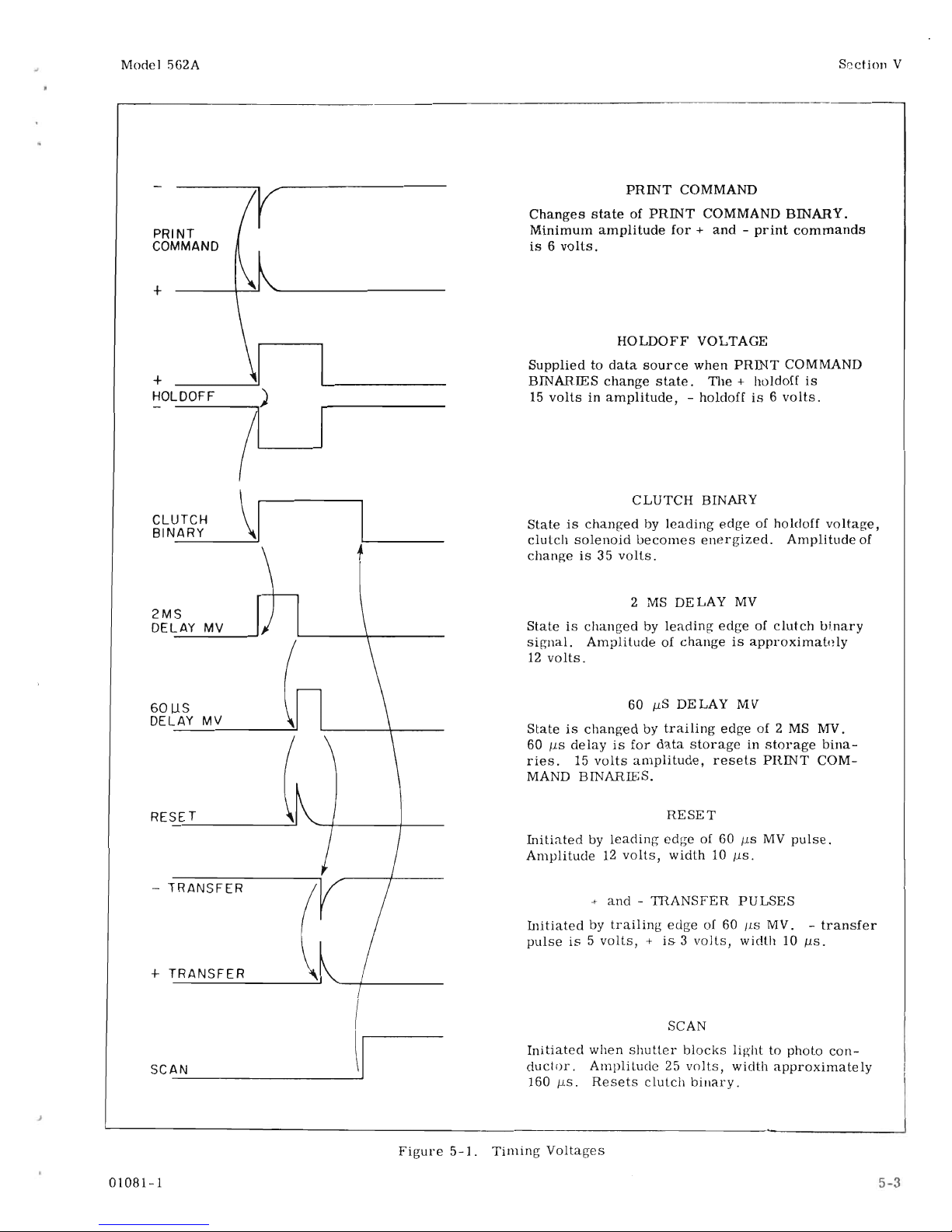
PRINT
COMMAND
+
+
HOLDOFF
CLUTCH
BINARY
2MS
DELAY
MV
GOUS
DELAY
MV
RESET
-
TRANSFER
+
TRANSFER
SCAN
-----------
01081-1
Section
V
PRINT
COMMAND
Changes
stateofPRINT
COMMAND BINARY.
Minimum
amplitude
for+and-print
commands
is6volts.
HOLDOFF
VOLTAGE
Suppliedtodata
source
when
PRINT
COMMAND
BINAR.IES
change
state.
The
+ holdoff
is
15
voltsinamplitude,
- holdoffis6
volts.
CLUTCH
BINARY
Stateischangedbyleading
edge
of holdoff
voltage,
clutch
solenoid
becomes
energized.
Amplitude
of
changeis35
volts.
2
MS
DELAY
MV
Stateischangedbyleading
edgeofclutch
bi.nary
signal.
Amplitudeofchangeisapproximatnly
12
volts.
60
IJ.S
DELAY
MV
Stateischangedbytrailing
edge
of 2
MS
MY.
60
IJ.S
delayisfor
data
storageinstorage
bina-
ries.
15
volts
amplitude,
resets
PRINT
COM-
MAND BINARIES.
RESET
Initiatedbyleading
edge
of 60
IJ.SMVpulse.
Amplitude12volts,
width
10
IJ.S.
+
and-TRANSFER
PULSES
Initiatedbytrailing
edge
of 60 /lS MV. -
transfer
pulseis5
volts,+is3volls,
width
10
IJ.S.
SCAN
Initiated
when
shutter
blocks
lighttophoto
con-
ductor.
Amplitude25volts,
width
approximately
160
IJ.S.
Resets
clutch
binary.
Figure
5-1.
Timing
Voltages
5-3
Page 24
Section
V
Table
5
-2.
-1248
Code
Model
562A
-
8
4
2
1
D
BINARY
C
BINARY
B
BINARY
A
BINARY
Character
BCD
INPUT
BCD
INPt.JT
BCD
INPUT
BCD
INPUT
0107
0108
0105
0106
0103
0104
0101
0102
1
0
off
on
0
off
on
0
off
on
1
on
off
3 0
off
on
0
off
on
1
on
off
1
on
off
5 0
off
on
1
on
off
0
off
on
1
on
off
7 0
off
on
1
on
off
1
on
off
1
on
off
9
1
on
off
0
off
on
0
off
on
1
on
off
-
1
on
off
0
off
on
1
on
off
1
on
off
Blank
1
on
off
0
off
on
1
on
off
0
off
on
8
1
on
off
0
off
on
0
off
on
0
off
on
6 0
off
on
1
on
off
1
on
off
0
off
on
4 0
off
on
1
on
off
0
off
on
0
off
on
2
0
off
on
0
off
on
1
on
off
0
off
on
0
0
off
on
0
off
on
0
off
on
0
off
on
BCD
INPUT:
"0"
is
zero
level
input,
"1"
is
one
level
input
Tab
Ie 5 - 3 . +
1248
Cod
e
-
+
8
4
2
1
D
BINARY
C
BINARY
B
BINARY
A
BINARY
Character
BCD
INPUT
BCD
INPUT
BCD
INPUT
BCD
INPUT
0107
0108
0105
0106
I
0103
0104
0101
0102
1
0
on
off
0
on
off
0
on
off
1
off
on
3
0
on
off
0
on
off
1
off
on
1
off
on
5
0
on
off
1
off
on
0
on
off
1
off
on
7
0
on
off
1
off
on
1
off
on
1
off.
on
9
1
off
on
0
on
off
0
on
off
1
off
on
-
1
off
on
0
on
off
1
off
on
1
off
on
Blank
1
off
on
0
on
off
1
off
on
0
on
off
8 1
off
on
0
on
off
0
on
off
0
on
off
6
0
on
off
1
off
on
1
off
on
0
on
off
4
0
on
off
1
off
on
0
on
off
0
on
off
2
0
on
off
0
on
off
1
off
on
0
on
off
0 0
on
off
0
on
off
0
on
off
0
on
off
BCD
INPUT:
"0"
is
zero
level
input;
"1"
is
one
level
input
5-4
01081-1
Page 25
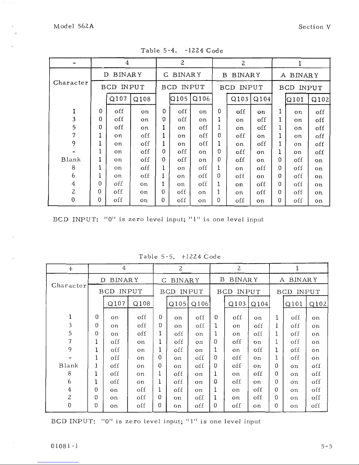
Model
562A
Section
V
Table5-4.
-1224
Code
-
4
2
2
1
D
BINARY
C
BINARY
B
BINARY
A
BINARY
Character
BCD
INPUT
BCD
INPUT
BCD
INPUT
BCD
INPUT
0107
Q108
0105
Q106
Q103
QI04
QI01
QI02
1
0
off
on
0
off
on
0
off
on
1
on
off
3
0
off
on
0
off
on
1
on
off
1
on
off
5 0
off
on
1
on
off
1
on
off
1
on
off
7
1
on
off
1
on
off
0
off
on
1
on
off
9
1
on
off
1
on
off
1
on
off
1
on
off
-
1
on
off
0
off
on
0
off
on
1
on
off
Blank
1
on
off
0
off
on
0
off
on
0
off
on
8
1
on
off
1
on
off
1
on
off
0
off
on
6
1
on
off
1
on
off
0
off
on
0
off
on
4 0
off
on
1
on
off
1
on
off
0
off
on
2
0
off
on
0
off
on
1
on
off
0
off
on
0
0
off
on
0
off
on
0
off
on
0
off
on
BCD
INP
UT:
"0"
is
zero
level
input;
"1"
is
one
level
input
Tab
1e 5 -
5.
+
1224
Cod
e
+
4
2
2
1
D
BINARY
C
BINARY
B
BINARY
A
BINARY
Character
BCD
INPUT
BCD
INPUT
BCD
INPUT
BCD
INPUT
Q107
Q108
Q105
QI06
QI03
QI04
QI01
QI02
1
0
on
off
0
on
off
0
off
on
1
off
on
3 0
on
off
0
on
off
1
on
off
1
off
on
5 0
on
off
1
off
on
1
on
off
1
off
on
7
1
off
on
1
off
on
0
off
on
1
off
on
9
1
off
on
1
off
on
1
on
off
1
off
on
-
1
off
on
0
on
off
0
off
on
1
off
on
Blank
1
off
on
0
on
off
0
off
on
0
on
off
8
1
off
on
1
off
on
1
on
off
0
on
off
6
1
off
on
1
off
on
0
off
on
0
on
off
4 0
on
off
1
off
on
1
on
off
0
on
off
2 0
on
off
0
on
off
1
on
off
0
on
off
0
0
on
off
0
on
off
0
off
on
0
on
off
BCD
INPUT:
"0"
is
zero
level
input;
"1"
is
one
level
input
01081-1
5-5
Page 26
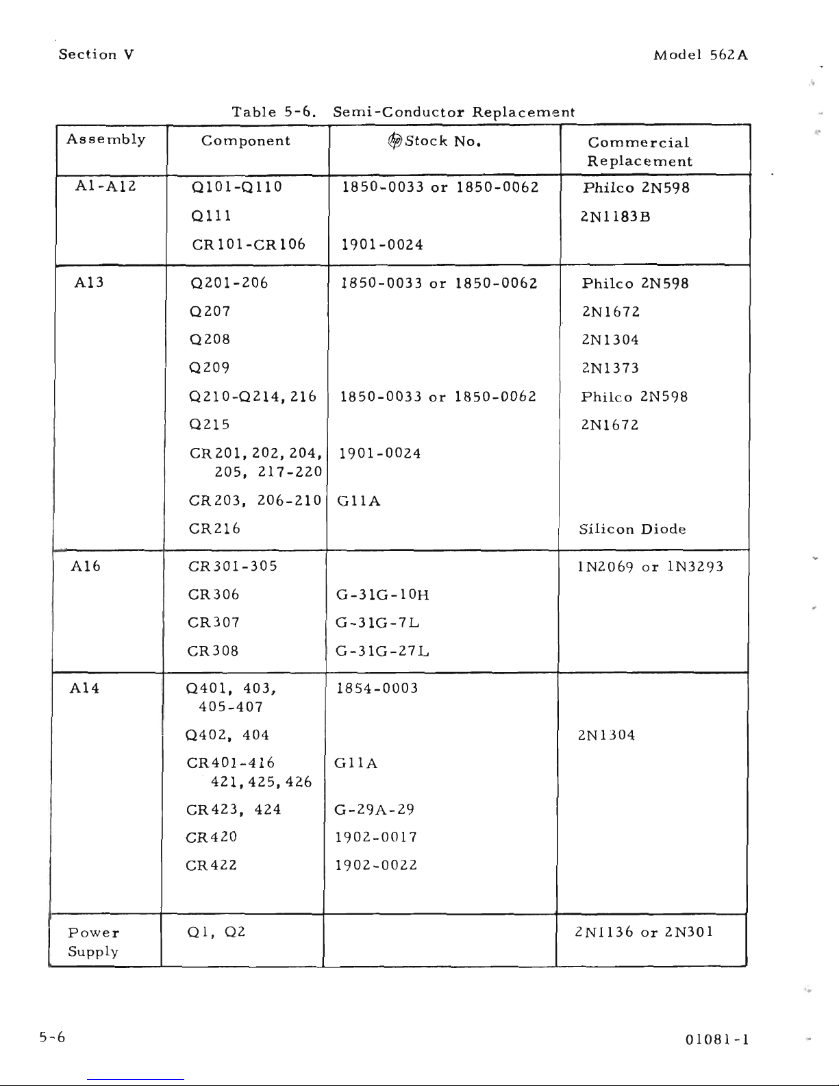
Section
V
Table
5-6.
Semi-Conductor
Replacement
Model
562A
Assembly
Component
~Stock
No.
Commercial
Replacement
AI-A12
0101-0110
1850-0033
or
1850-0062
Philco
2N598
0111
2Nl183B
CR10l-CR
106
1901-0024
AI3
0201-206
1850-0033
or
1850-0062
Philco
2N598
0207
2N1672
0208
2N1304
0209
2Nl373
0210-0214,
216
1850-0033
or
1850-0062
Philco
2N
598
0215
2N1672
CR201,
202,
204,
1901-0024
205,
217-220
CR203,
206-210
GIlA
CR216
Silicon
Diode
A16
CR301-305
lN2069
or
IN3293
CR306
G-31G-10H
CR307
G-31G-7L
CR308
G-31G-27L
A14
0401,
403,
1854-0003
405-407
0402,
404
2N
1304
CR401-416
GIlA
421,425,426
CR423,
424
G-29A-29
CR420
1902-0017
CR422
1902-0022
Power
Ql,
Q2
2N1136
or
2N301
Supply
5-6
01081-1
Page 27

Model
562A
Section
V
Figure
5-2
r-------
+-
-19V
+
...
-----....,
DISABLE
VOLTAGE -
...
-----.,
"A"
INPUT
--.----,
INHIBIT
GATE
~
CRI05,CRI06
AMPLIFIERS
0109,0110
---------,
STORAGE
f-+--
GATE
I--~
BINARY
CRIOI
0101,
0102
f--+-
BRUSH
f---...--
DECODI
NG
1--1:::::)--0------,
STORAGE MATRIX
~
g~ro~
f---+-
BINARY
R161- H
0107,
L..........-
RI96
L-f"\
0108
~
~
~
~
~
f----o
~
AI - A12,1-2 - 2- 4 CODE
---------
,
I
I
- REF.
VOLTAGE
+ REP
VOLTAGE
......
L...-~-J
"D"INPUT
_.--_-J
1
+ TRANSFER
PULSE
-TRANSFER
PULSE
TRANSFER
AMPLIFIER
0216
~
DELAY
TRANSFER
PRINT
SCAN
AMPLIFIER
"AND"
CWTCH
MULTIVIBRATOR
DELAY
SCHMITT
~
0207
GATE
f-+-
BINARY
f-+-
(2MS)
~
MULTIVIBRATOR
0205,0206
0208
0209,0210
(60
US)
~
0211,0212
0213,0214
I
SCAN
~
....-
-19V
L515
V501
~DI5HU~TER
I @05501 .
L__- - - - - -
---
--EJ-----
~~T~~A.'l,~o~NO
I
I
PRINT
COMMAND
BINARY
NO.1
0201,0202
PRINT
COMMAND
~.----I
NO.1
DISABLE
VOLTAGE -
+-
---J
+.--_1
PAWL
MAGNET
AMPLIFIER
0111
80-E-80
PAWL
MAGNET
,-
I
I
I
I
I
I
I
I
____
--.J
TRANSFER
L..-.-
AMPLIFIER
I---+-
0215
GATE
STORAGE
-
REF.
.....
CRI02
I--
r-.
BINARY
VOLTAGE
0103,
0104
I---+-
'B'INPur
I
t
STORAGE RESET
I
f--+-
GATE
STORAGE
......
f--
f-.-
BINARY
-
REF.
CRI03
0105,
VOLTAGe:
0106
---.-
"C"INPUT
I
~
I
SCAN
I
L
_________
PRINT
COMMAND
BINARY
RESET
PRINT
COMMAND
BINARY
NO.2
0203,0204
PRINT
COMMAND
--1_---1
NO
2
01081-1
Figure
5-2.
Functional
Block
Diagram
5-7/5-8
Page 28
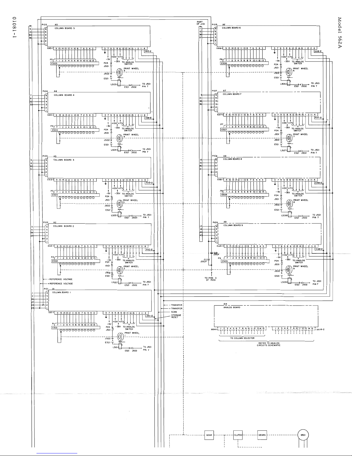
o
~
o
00
~
I
~
PART
A5
OF
JIOI
P05,.------=A~6
_
9
COLUMN
BOARD
5
II
6
COLUMN
BOARD'6
10
12
5
~
~
:
2
,
t t t t
t +IOV +17V t +IOV +17,(. • •
.)
-9V
t
~
t
--y-
P24
-35V
TO
ANALOG
-911
-35V
TO
ANALOG
l-
_
J501
II
SWITCH
P24
4
SWITCH
__
.---------------------j502-
__
~-~~~T-~-H~~L---------
__
---------1--------
---------------------~:~r--
~:RINT
WHEEL
6
~
I 9
~
E521
~
I
E521
~
L505
y----Hr--
TO
J501:
L506
~,,>----
TO
J501
E521
J502
PIN 7 I
E521
J502
PIN
7
~
o
0.
ro
~
U1
0'
N
>
I
I
I
--I
I
I
8 6
12
13
14 15
I Z
II
4
~~~~
••
A_
--------,
I
I
,
'"
.,'~."J
L.'-'-T-'-rT-'-''T,-,,.-r-J
XA14-2
I I I I I I I I I I I I I
I I I I
t I I I I I I I I
--
- l
A7
COLUMN
BoARD 7 - - - I
PIOB
3 7 9 5
+'ltltlllll'~
t
+IOV+17V
~
-9V
t
~
- 35V
TO
ANALOG
P24
SWITCH
3
_____________________
~;;2-f
__
@)
:RINT
WHEEL
E521~
L508~4>--
TO
J501
E521
J502
PIN 7
REFER
TO
ANALOG
CIRCUITS SCHEMATIC
AI4
1,,"0;;0;:;;0
--
I
I
~3-
4-
5~9Ki"
i'2i3i4i5
"T
XAI4-'
..
,_,....
T
-'-rT
,-,-
r""
T'
-'-.-r
...
• I t I I I I I I I I I , I I
I
•••
I I I I I I I I I I I
, J
TO
COLUMN SELECTOR
\ J
STORAGE
RESET
I
I
III
I
I
I
----------~-------
III
--
-----
I
I
: -
g-
gOUF
+I~V
+I~V
:
t~
I CII
-35V
TO
ANALOG
l..-
_
I
.05UF
9
SWITCH
-.-
--
-- --
-
-+
------
--
--
----i-
-
------
--
-----
--.
-
----
--
--------
---::~
r~;
-~'"'
W"
I
TO
PINS
3
:
OF
P201
L509
4>--
TO
J501
:
E521
J50Z
PIN 7
I
-
--------~
I
UE
TRANSFER:
+ TRANSFER
SCAN
I
I
I
--~_
...
-
. -
~-~
-1-
~
-
--
- - - -
--+-
-
-----
-.-.---.-
COLUMN BeARD 4
XA3-1
t
-9V
P24
12
_________________________
;:;~l-
_@)~~I~~_~HEEL
13
E521~
L503~4~
TOJ501
E521
J50'>-- PIN 7
fo---
...
REFERENCE
VOLTAGE
PI04
1
A4
I
t t
_~
+IOVt+17~
P24
-35V
TOS~~:MtG
.......
----
J501 1
5
______________________
J502-
@)_:~~N~
_WHEEL
3
E521
L........A
L504~4~
;~JiO'
H-+REFERENCE
VOLTAGE
PI(
7
IE501
~~
'-
M
:~W
••
'0,",' I
t t
+IOV +17V
t~
-35V
TO
ANALOG
.......
----
PZ4
SWITCH
6
----
...
-~~~I-
_-@)-~~~~_
~~~E_L
_
E521
10
c::;::>...."-
~4>-TOJ501
E521
J502
PIN
7
Page 29
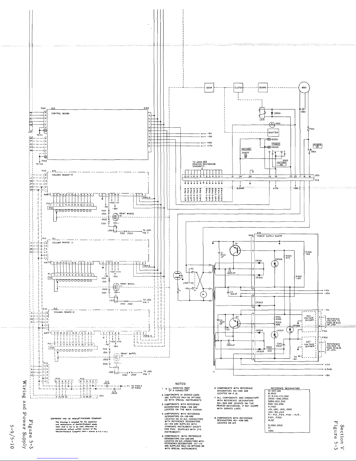
• I
I'
I I
IpOWERI
ON
PS501
EjF501
R306
150
.....-
B501
~~I
~
R305
1.2K
R304
470
S50Z
IRECORDI
ON
c£5306
!.1:\V501
L.....4-
HJ_C_R_50_1
__
--,
L515
"-7
-
-I
SHUTTERI
0:
DS501
IpOWERI
DS50Z
hP
AI6
POWER
SUPPLY
BOARD
CR303
XA~
IRECORDI
DS503
@
-J------.j
41
'"
I
I
III
L
,_
• I !
I!
t=!=j
~
>'0'
~
-35V
r 8 •
, ,
13
1
1>
I
'~
-9V
.-
- - - - -
-:
'I
i-----+
R-
3
-
O
-I
--·--'1
VO~~~GE:
3
r-}
REFERENCE
ZZOO
I DIVIDER I I
~?NLJA2~E6Tf5
R30Z
+:
: I
OF
JIOI
...
~----">Z50
_
C~.-L
- -
-:-7
_
CR307
L'
J
",P301
8
r------i
':P30Z
15
I REF : 3
~}
REFERENCE
II~
C301
I VOLTAGE I :
VOLTAGE
TO
1~60UF
RJ03
40UF
~
DIVIDER I :
~~N~lO'I6
Z5
L-+
-,
Z
CR305
ZZO
::
4 ~
..------,9
TO
.-JL
~
)
6
-9V
......--+--~-,
+17V
tj
R301
·52
I::
CR30Z
TO
J50Z,SEE
PRINTER MECHANISM
SCHEMATIC
t
en
en
en
z
z
z
Ci:
Ci:
Ci:
~
~
~
1111111111111
I I
~
~__:_-:-'7"7-~:--:::'"'7--_::_--:":--::":""----_:":-~---__=__:"::__:~:_::___:::~
J501
'-T-r-,--r-,..,,.,.....,...-,--r--r-,-,.---,---,.---,-------,.--,----....,...--,r-..-
...
-.--'
PZ4
cmu_-Lu
uu
amT-+~,"~_m_--1
"'"
~
-u - - n u _
uu
I
I
L----------
1
,--,
f--
PZOI
AI3
XAI3
~
~;
_ :
CONTROL
BOARD
-:
~
4
III--
I
ZI-~H
Z
II-I-I-H
C~
15
I
JIoI
J.
..
~
10
I
r.,
TOCII
~
~
I _
=~9~
~~~==~:
IZ
: 1
:ZZ:---~4
: I 1
:II~~
:23~---i
I I
:48:----1
Z
:i
tr-~11,-
----'
: I
PZOZ
I :
TO
CIZ
I I
I I
I I PliO AIO
: I
~--_.'61-~0~B~;R~
--
--
--
--
--
--
--
--
--
--l
:Z:----:51
:
:Z6:---~
4
,
,21~---131
:Z4'---r-:
2
J
:Z5:
1
/,:
_
I I I
XAIO-lo......;'-T-T--r--r-T-'1r---r-r-r--r-.,..;r--'
: I
Itt
I:
I I
I I t +IOV
+17
:
I I
-9V
t . '
I I PZ4
-35V
'-7-:
---------------------------------
i
II
- - - - - - - - - - - - - - - - - - - - -
~:~~
1-
@}
~~~
_W_H~~L_
- - - - - - - - - -
-.
-
-.
-
~
I 8 I
I
II
E5ZI~
: I
II
L5ID~4>___TOJ501
IIII
:
I I
E5Z1
J50Z
PIN 7 :
I I '
I I I
Pili
All
:3~.J-t-.(6r
~N
·B~A~
--
--
--
--
--
--
--
--
--
--
--l
'4r-..l-t
45
:Z8:-.J.-t
~
4,
'Z91-...1-t.,
3'
I
t-lZk
tt
J
,
..
XA1H
9
-15
1~10-8-
765
4
-3
I I
+IOV
+17V
I
-9V
-35V
, ' I
PZ4 8 I I
-
;~~~
1-
®
~~~~T_
~~~E_L.
- - - - - - - -
-.:
.!.:
-
.!
--1
E5Z1
~"
"?-
I I
\ I I
'I
I
::
I I
L511
4>___
TO
J501
I "
I,
I I
E5Z1
J50Z
PIN
7 I
I,
I I I
i
5~_:-I:~f
~~WM-N-
BOARD
1;-
--
-.
--
- -
--
- -
--
- -
--
-·l
i :
16~_1_~:51
I I
:3d,--1-1-:
4,
, I I
:31r--J-I~JI
, I I
I:
I
t-:
21
.. J I I
::
ti\!L
~_.
'~~
~-:.
, .
,-n-"
I I I XA12-1' 9
15
14
13 12
II
10
8 7 6 5 4
3'
'3
7 9 5 8 6 I 2 II 4 ' I I I
::
I I L-rYrrr-r-l-rrl-r-iTJ
'-TT1-rTr-------rrr[X~Il:~J
I I I
I I
I:
I I I I I I I I I I I I I v I : I : t I I L J I I
: I I
PZ
J.LLLJ_LLLL.LLLl.
I
1+IOV,17V
I L J I
I I I I
:_(_7_~_~_3_~_~_6
__
8_?_I.9_I~!Z_I~.'.......
-9V
1
-35V
L J
I
I'
E51Z
,
-+-
: I I
~
--
-r
tf'-t:'
-t:;
;:rt..)
r:,-~:,
-~:;
;
..
:'
U t.",
...
:,- -
-"
P24
I
I I 1 1 J501 r "
-;-\
PRINT
WHEEL
: I I I
~-----------------------------+-;.:~:;
rl~.-------------.--.--------
I I
L-J
J50Z';'
..:....:
::
I
P"~,
E5Z1
Y
c~:J
_
Page 30
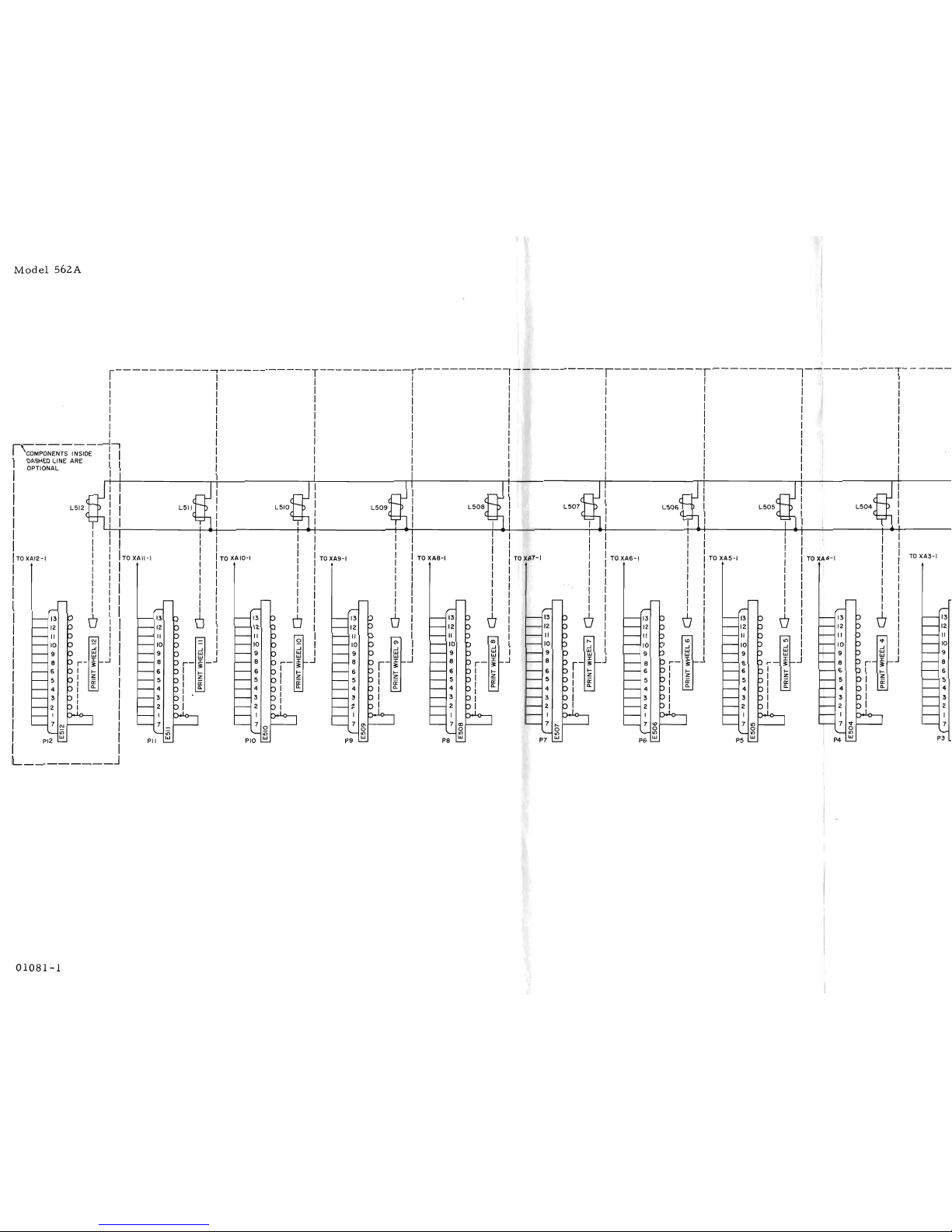
Model
562A
P3
L504
<t'
o
LO
P4 W
L505
LO
o
LO
P5 W
L506
L507
,....
o
LO
P7 W
I
I
I
I
I
I
I
I
I
I
I
I
TO
XA7-1
I
TO
XA6-1
I
TO
XA5-1
I
TO
XA4-1 I
TO
XA3-1
I
I
I
I
I
I
I
I
I
I
I
I
I
I
I
I
I
I
I
I
I
I
I
I
I
I
I
I
I
I
I
I
D
0
Q
a
D
<t'
..J
W
...J
~
~
W
::t:
~
~
z
ii:
CL
L508
TO
XA8-1
13
12
II
10
9
-l
8
6
5
4
3
2
I
7
IX)
o
LO
P8 W
I
I
I
I
I
I
I
I
I
I
(]
L509
P9
TO
XA9-1
...J
I
I
I
I
I
I
I
I
I
I
o
L510
13
12
II
10
9
8
6
5
4
3
2
I
7 0
in
PIO W
TO
XAIO-I
L511
I
I
I
I
I
I
I
TO
XAII-I
I
I
I
I
I
I
I
I
I
I
I
I
I
I
I
I
(]
0
=
-.J
L512
13
12
II
10
9
8
6
5
4
3
2
I
7 N
LO
PI2 w
TOXAI2-1
I-----------~-----------T-----------r----------'----------I----------I---------I----------T~-----
I I
I I
I I
I I
I I
I I
I I
n------~,
I
I 'COMPONENTS INSIDE I I
DASHED
LINE ARE I I
OPTIONAL I
I
I
I
I
L J
01081':"1
Page 31

Section
V
~
Figure
5-4
5501
/
rt'l
>
rt'l
>
U
U
.....
et
~
et
~N
-
etO
a:
>
>
0
x-
+
x_
~
~
~
~z
~z
0-
0-
a::
CL
a::
CL
~
~
05501
).
V501
L515
F501
REFERENCE DESIGNATION
8501
C501
CR501
OS
501-
503
E501-512,
E521
F501
J5Ql
t
J502
L501-512,
L515
PI-
PI2,
P24
V501
L ---------1
SHUTTER
I
~
I
POWER
I
0()
I
05502
<5
0()
I
RECORD
ON
I
-J
~
0
rt'l
0()
.....
(7l
a::
N v
ID
CD
~
(5
0
0
0
0
=
~
0 000
~
IRECORD
ON
I
5502
0()
0()
0()
0()
0()
0()
0()
0()
0() 0() 0() 0()
---------
-J
-J
-J -J
-J
-J
Z
-J
-oJ
-J
-J -J -J
0
05503
~
~
~
~
~
~
~
~~~ ~ ~
~
0
0
0
0
0
0
~
0
0
0
0
0 0
a::
a::
a:: a::
a::
a::0a::
a:: a::
a::
a::
a::
~
~ ~
~
~
~
u
~ ~
~~~
~
L505 L504
L503
L502
L501
I
I
I
I
I
I
I
I
I
I
I
I
TO
XA4-1
I
TO
XA3-1
I
TO
XA2-1
I
TO
XAI-I
I
I
I
I
I
I
I
I
I
I
I
I
I
I
I
I
I
I
I
I
I
I
I
I
I
I
I
I
I
I
I
6
D
6
6 D
v
N
-J
W
.J
w
J:J:
~
~
z
a:
CL
:)
v
0
:>
0
:)
0()
0()
...
w
PI
w
P4
COPYRIGHT
1961
BY
HEWLm
·PACKARD
COMPANY
(7l
(7l
(7l
(7l
(7l
rt'l
U
(7l
(7l (7l (7l
(7l
(7l (7l
~o()
et
Thil
drawingilintended
for
the
operation
Z
z
~
z z
z
z z
z z
z
z
~
and
maintenance of
Hewlett.Packard
equip.
ii:
ii:
n-
ii: ii:
ii:
ll.
ii: ii: ii:
ii:
ii:
x_
ment
and
il not tobeuled
atherwile
or
N
N
N
N
N
N
N
N N
N
N
N
~z
j
I I
I
I
I
I
I
I
I
I
0-
reproduced
without written can
lentofthe
I
I
Q
N
a::ll.
~
rt'l
0()
.....
(7l
N
V
ID
CD
~
Hewlett·Packard
Company.
562A-P.M.-T-12IC
et
et
et
et
et et
et
etetet
et
X
X
X
X X XXX
XXX
X
--------T-----------,-----------T----------T---------~-,--~---~----------------
I l I I
I I I
I I L •
I
I I
I I I :
I I
1------.---------,
I I
CR501
I I
Figure
5-4
Printer
Mechanism
5-11/5-12
Page 32
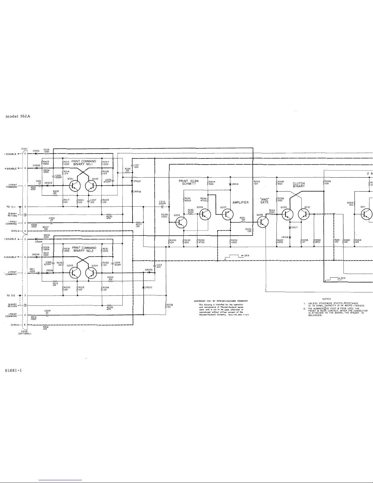
Model
S62A
P202
(OPTIONAL)
P201
R202
r-
CR201
1000
-
5
~
R203
R215
PRINT COMMAND
R227
CR202
390K
1200
BINARY
NO.1
1200
:::~C211
-
4
....
.001
R236
R204
R216
R228
l,qK
2 M
1000
12
K
12K
::~~?g~F
0201
0202
C201
4~6~~:::~
,
CR207
PRINT
SCAN
R244
R253
R255
R259
R2
.01
CR203
-
SCHMITT
560
j~
CR216
15K
560
CLUTCH
10K
,
BINARY
101
-
I
~
CJ
R201
J'I
1000
R205
CR208
15K
.-
R256
~
R241
R245
"AND"
R217
R221
,I..-C207
R229
8200
4700
560
10K
100
';:~IOO
10K
C210
AMPLIFIER GATE
R263
200PF
10K
I
I'
0206
o~
o~
~
0211
3
.,
R242
R254
5600
1000
@
R239
0205
~
0208
~
c9
R230
1000
R251
C202
47K
15K
2
.~I
~
~
-
II
R237
R206
1000
R207
15K
,~CR217
10K
R252
-
15K
6
>-
R208
(
...
1
1000
CR218
A~
+-,
5
R240
..
R243
R246 R250
R257
R258 R260
R261
R262
R264
CR204
47
..
1800
10K
10K
18K
I
10K
820
4700
1000
1000
I
I
R209
PRINT COMMAND
I
390K
R218
BINARY NO.2
R231
I
1200
1200
I
CR204
R210
~25V
I
...
1000
+-1
4
I
....
/
I
I
C2.06
...
L"
R219
~l:2
:::
~~;g~F
I
4.70PF'::"'"
:::~.%~1,2
I
12K
0203 0204
I
I
R211
CR206
CRI~09
I
1000
"
-
__
.J
I
.
....
I
71
I
R233
~5V
I
10K
~.
I
I
R212
I
15K
, CR210
I
R220
R222
R234
I
10K
100
10K
I
I
-,~
3
I I
NOTES
I I
COPYRIGHT
1961
BY
HEWLETT
·PACKARD COMPANY
UNLESS OTHERWISE STATED,RESISTANCE
I I
This
drawingisintended
for
the
operation
I.
..
L~
@
R238
IS IN
OHMS,
CAPACITYISIN
MICRO -
FARADS
R235
15K
and
maintenanceofHewlett·Packard
equip·
2.
PIN
NUMBER
@OF
P2076P208
USES
THE
I
47K
ment
andisnattobe
used
otherwise
or
FRONT 6 REAR CONTACT. WHEN THE CONNECTOR
I
C204
reproduced
without
written
consentofthe
IS
ATTACHEDTOTHE BOARD, THE BINARY IS
I
.£>1
I
Hewlett.Packard
Company.
562A
CTRL.IlRD.-T-12IB
BALANCED.
--.,
2
II
I
R21~
I
100
I
I
~--i
6
I
R214
,--
10K
SCAN
BINARY
RETURN
BINARY
RETURN
TO C
II
+PRINT
COMMAND
TO
CI2
SCAN
- PRINT
COMMAND
+PRINT
COMMAND
-PRINT
COMMAND
+DISABL.E
-
DISABLE
-DISABLE
+.DISABLE
01081-1
Page 33
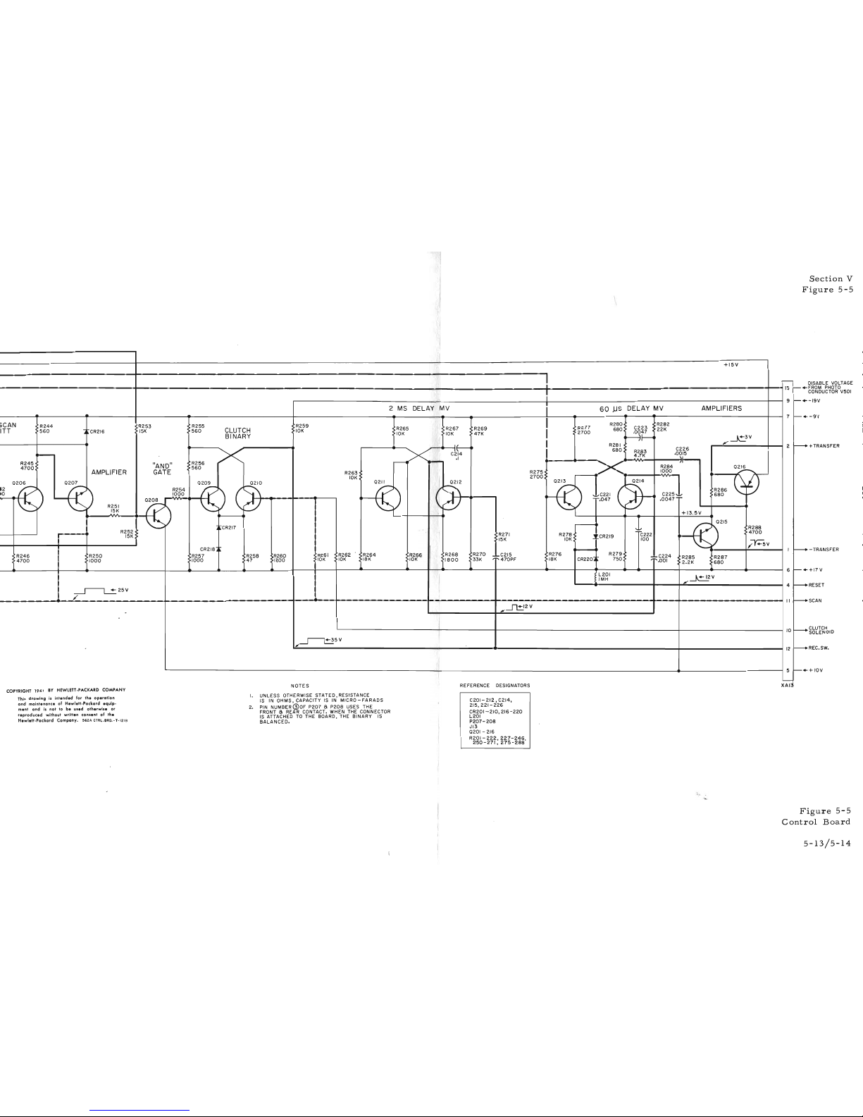
Section
V
Figure
5-5
\
\
I
+15V
.----
DISABLE
VOLTAGE
15
f--+
FROM
PHOTO
CONDUCTOR
V501
9
f--
..
-19V
7
-
..
-9V
2
f----
+TRANSFER
R288
4700
,-y;:sV
I
f---+
-TRANSFER
6
f--
..
+17V
4
-
RESET
II
-
SCAN
0216
R286
680
AMPLIFIERS
+13.5V
C226
.0~)5
R284
1000
c2251
.0047
"""
R282
22K
R285:R287
2.2K•680
:::~
C222
100
60.uS
DELAY
MV
).R277
R280
680.
C223
2700
.0~~7
7r
R281
680
R283
4.:7K
I
mg:
j
Q~~C221
~
-.Q47
'---+---+---4..---1~-~~,:",:::":,,::,,:,,,,--a
>R269
47K
•
R267
~
10K
I
I
I
.--
R271
R278
~
CR219
15K
10K
R266
•
R268
R270
....
C215
R276
R279
10K
1800
33K
'r-
470PF
18K
CR220~
750
L201
IMH
.(
R265
~
10K
2 MS DELAY
MV
0211
R263
10K
;CAN
R244
R253
R255
R259
ITT
560
-;~CR216
15K •
560
CLUTCH
10K
BINARY
.-
R245
"
AND
"
R256
4700
560
AMPLIFIER GATE
0206
O~
0209
~
~2
R254
W
lO
1000
~
~
0208
~
CJ
R251
15K
R252
HCR217
15K
CR218
~
R246
•
R250
R257
R258 R260
4700
1000
1000
47
/800
~25V
/
'"
11'~5V
wo..
-:-
..:..
...
~-
-----------....J
12
_REC.SW.
5
f--++IOV
COPYRIGHT 1961BYHEWLETT
.PACKARD
COMPANY
This
drawingisintended
for
the
operation
and
maintenanceofHewlett·Packard
equip.
ment
andisnot tobeused
otherwise
or
reproduced
without written
consentofthe
Hewlett.Packard
Company.
562A
CTRL.BRD.-T-12IB
NOTES
I.
UNLESS OTHERWISE STATED,RESISTANCE
IS IN OHMS, CAPACITY
ISINMICRO -
FARADS
2.
PIN
NUMBER
@OF
P2076P208
USES
THE
FRONT
6 REAR CONTACT. WHEN
THE
CONNECTOR
IS
ATTACHEDTOTHE BOARD, THE BINARY IS
BALANCED.
REFERENCE DESIGNATORS
C201-
212,
C214,
215,221-
226
CR201-210,216-220
L201
P207-
208
JI3
0201 -
216
R201-
222,227-246
250-271,275-288'
~
XAI".I
Figure
5-5
Control
Board
5-13/5-14
Page 34

Model
562A
Section
V
Figure
5-6
o
I
'0
S6
I
>PINI2
r-IC~A-L1~B--R-AT""E"'1
:
0-
10PERATEI
-o-l.o
IZERol
55A
558
S5C'
S5D
S5A
S5B
S5C
S5D
S5A S5B
SSC
5SD
ol
0-1
oJ
oJ
cr-
XAI-2'
cr-
XAI-2'
0-
XAI-2'
0-
XAI-2"cr-
XA2-2"
cr-
XA2-2"
0-
XA2-2"
0-
XA2-2"
cr-
XAI-2
0-
XAI-2
I
0-
XAI-2
0-
XAI-2
0-
XA2-2
cr-
XA2-2
0-
XA2-2
0-
XA2-2
0-
XA3-2
0-
XA3-2
0-
XA3-2
0-
XA3-2
0-
XA2-2
0-
XA2-2
0-
XA2-2
0-
XA2-2
0-
XA3-2
0-
XA3-2
0-
XA3-20-
XA3-2
0-
XA4-2
0-
XA4-2
cr-
XA4-2
0-
XA4-2
0-
XA3-2
cr-XA3-2
o-XA3-2
o-XA3-2
0-
XA4-2
PINIScr-
XA4-2
>PINI40-XA4-2
>PINI30-XA4-2
PINI20-
XA5-2
PIN
ISO-
XAS-2
>PINI4cr-
XAS-2
>PINI30-
XA5-2
0-
XA4-2
PINISo-
XA4-2
>PINI40-
XA4-2
>PINI30-
XA4-2
>PIN
120-
XAS-2
0-
XAS-2
0-
XAS-2
0-
XAS-2
0-
XA6-2
cr-
XA6-2
0-
XA6-2
0-
XA6-2
0-
XAS-2
0-
XAS-2J
0-
XAS-2
0-
XAS-2
0-
XA6-2
0-
XA6-2
0-
XA6-2
0-
XA6-2
0-
XA7-2
0-
XA7-2
0-
XA7-2
0-
XA7-2
0-
XA6-2
0-
XA6-2
0-
XA6-2
0-
XA6-2
0-
XA7-2
0-
XA7-2
0-
XA7-2
0-
XA7-2
~
XA8-2
0-
XA8-2
0-
XA8-2
~
XA8-2
XAI4_~~_XA=2_
F:-~
_F:7:
-F
~A~-~
-F_XA_~-~
-F
~:-~
-F~A:~F
~A:2_
-F
~:2~
FX:-~
~F
~A:2~
-r
XA9-2
I 9 10
II
12
S 6 7 8 I 2 3 4
IS
13
14
I
I
A
15~
13
~.
CR426j~CR427
7
I
+
-
9V
ANALOG CKTY
1224
CODE
T161A
COPYRIGHT
1961 BY
HEWLETT
- PACkARD COMPANY
R457
IK
R455*
R456
•
56K
-9V+-...------...
*
R453
R454
33K
~+17V
~~
CR425
I
t
+17V
14
)
12
R452
lOOK
3
I
GALVANOMETER I
/ <
RECORDER
/ > PART
OF
t>
<;>c
/
L--...J
J31 J31
/1
~
- - - - - - - - - - - - -
_/
BALANCEDDCAMPLIFIER
15
10
R445
R450
2.7K
2.7K
- 9 V
....
- ......
-----+---------,
--
.....-----4
0405
Q
406
~
~
r;;
~
.....
.....
~
CJ
Q407
CR423 CR424
~
+17V
R451
Il
10K
R444
10K
R49
2.7K
_
R440
2K
R438
3.9K
R441
R442
R443
2.7K
6.2K
1.2K
'*
+17V
II
I
GALV.
ZERO I
RI2
2K
DIFFERENTIAL
AMPLIFIER
R406
R408
R410
R412
22K
22K
22K
22K
R427*
*
*
,
*
*
R407
R40
R411
R413
: R41S
R417
R419
R425
1M
2M
2M
4M
•
3K
6.2K
6.2K
12K
R428
123K
R414 R416
R418
R420
R426
REFERENCE DESIGNATORS
900K
300K
600K
600K
1.2M
C401-406
CR402
A~
CR404]r
CR406~~
CR408~~
CR410~~
CR412~.
CR414
~~
A~CR416
CR401-416,420-427
'~CR401
,~R4IS
J14,
31,34,35
~~CR403
~[CR40S
~~CR407
~~CR409
~'CR411
~~
CR413
.....
~
0401-
407
RIIA,
IIB,I2,
R401-420
..
42S-
428,
430-445
450-457
S5A-50,
S6
R405
20M
R437
560
0403
~
R404
4.7M
+II V
R403
2.4M
J(CR421
r--...
*
R436
~
\
3.3K
CJ
0401
~
1-if--+----+---
......
--'\II\I'Ir----+-----.
0402
::!.J
+17V
SERIESREGULATOR
R434
2K
R431
33.2K
R430
33.2K
R433
33.2K
R432
33.2K
R429
33.2K
2
R402
2.4M
4
R401
1.2M
R435
16M
.,
"
C401
.05
II'
C~02
.05
II'
C403
.05
If
,
C404
.05
If
C~05
'*
.05
I 9
J35>--
I
....
P-O-T-E-N-TI-O-M-E-TE-R
....'
~
RECORDER
~
01081-1
Figure
5-6.
Analog
Circuitry
5-15/5-16
Page 35

Model
562A
,-------------
RI66
JIOI
OR
J20
I
"I"
LEVEL
"0"
LEVEL
ALL MATRIX RESISTORS. INSIDE DASHED
RI72
RI84
T
RI92
T
LINES
ARE
33K,
1/4W!
5"10
RI67
EXCEPT
RI78
T
RI85
T
RI93
T
RI64,
RI65, RI66,
RI67,
R172.
RI77,
RI78,
RI83
RI68
RI84,
RI85,
RI86
,R187,
R192.
RI93,
R194,
RI95
~~7.3
T
I
WHICH
ARE
47K,I/4W!5"10
RI88
RI69
I
I3L7.9
T
':<~t1~
T
RI70
RI74
~
RI71
RI80
T
~
RI60
.
R18}
T
~
RI61
RI75
RI'
RI62
~
RI82
T
RI90
T
RI63
RI76
RI91
T
RI64
RI83
T
RI86
T
RI94
T
RI65
RI77
RI~7
T
RI95
T
L
-----
----
---
----
---
----------
----
-
---
-
------
--
----
---
---
----
---
--
RI04
A
BINARY
RI07
RII3
B BINARY
RII6
RI27
C BINARY
RI30
RI36
D BINARY
RI39
2.4K
2.4K
2.4K
2.4K
2.4K
2.4K
2.4K
2.4K
RI05
0101
0102
• RI08
RI14
0103
0104
• RII7
RI28
0105
0106
:
RI31
RI37
0107
0108
RI40
18K
18K
18K
18K
18K
18K
8K
18K
r-
RIOI
CI02
CI04
CI06
CI08
1
22K
CRIOI
.0,1
7
CRI02
'~17
CR..!.03
.~'7
CR.!.24
.Oj7
6
~
1\
1\
1\
/,
•
•
•
•
;;:,,~gl
RI02
RI03
RJ06
RI09
Rill
RI12
RII8
RI20
RI26
RI32
RI34
RI35
RI38
RI41
270K
10K
10K
10K
270K
10K
10K
270K
10K
10K
270K
10K
10K
10K
2
RII5
5
..
10K
RIIO
~;::CI03
RI29
22K
.001
RI19
10K
4
22K
4
<
'"
~.'6gI5
RI33
8
'22K
3
-REF.
2
+REF.
1
,~~gr
'--
P101-P1I2
I
RI42
1
47
~
COPYRIGHT
1961
BY
HEWLETT
.PACKARD
COMPANY
This
drawingisintended for
the
operation
and
maintenance
of Hewlett.Packard equip·
ment
andisnottobe
used
otherwise or
reproduced without written
consentofthe
Hewlett·Packard
Company.
562A
(-1248
CODE) CLM
BRD-T-121A
01081-1
Page 36
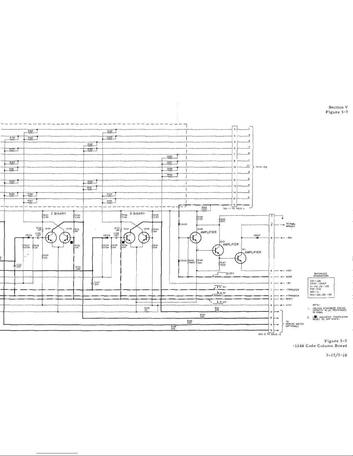
Section
V
Figure
5-7
REFERENCE
DESIGNATORS
C101-108
CRIOI -
CRI07
JI-~J12.J21-J32
P101-P112
0101-111
RI01-120.
126
-152
I.
NOTE:
UNLESS OTHERWISE STATED
CAPACITY
IN
J,JF.
RESISTANCE
IN
OHMS.
2.
(.)
INDICATES TRANSISTOR
RESET
TO
OFF
STATE.
TO
ANALOG
SWITCH
(OPTIONAL)
-
SCAN
_TOPAWL
MAGNET
-
-35V
- +TRANSFER
-
RESET
-
-9V
- +IOV
- -TRANSFER
-
+17V
...---
1--"
3
RI84
T
RI92
T
!
4
3
RI78
T
RI85
T
RI93
T
5
5
RI88
T
6
7
~L7.9
T
~~lt9
T
7
9
RI96
T
.
-
RI80
T
RI97
T
8
10
0
>-
TO
PI-PI2
R18}
T
RI98
T
II
8
RI99
r
12
6
RI82
T
RI90
T
13
4
RI91
T
14
2
RI83
T
RI86
T
RI94
T
15
0
RI~.7
T
RI95
T
9
-
----
-----------
--
----
--
----
----
---
----
_...J
RI44
r
\AI-I-'TOxA,I2-1
--'
220K
RI27
C
BINARY
RI30
RI36
o
BINARY
RI39
-
3
n
2.4K
2.4K
2.4K
2.4K
RI45
2.2K
RI52
-
820
"'CRI05
9
~
RI28
0105
0106
RI31
RI37
0107
0108
RI40
0108
18K
18K
8K
18K
rv
AMPLIFIER
CI06
CI08
CR.!..03
.q'7
C~.!..04
.Oj7
CR'.2
7
8
-
"
J'I
~
...
•
•
0110
RI20
• ,R126
RI32
RI34
RI35
RI38
RI41
tV
AMPLIFIER
270K
10K
10K
270K
10K
10K
10K
-
0111
,/
~
AMPLIFIER
..
RI29
rv
9
10K
K
j~CR106
RI43
RI46
~
390K
22K
RI47
..
,~gp
1000
RI33
'22K
5
~
~25V
~
(
II
I---
~~~gr
7
~
~5V
I
-
~3V
JI'
2
-
4
-
'~2V
I
6
-
RI42
RI51
47
22K
_
......
12
RI50
22K
13
r--
RI49
22K
>
14
r--
RI48
22K
15
r--
-
XAI-2TOXA12-2
Figure
5-7
-1248
Code
Column
Board
5-17/5-18
Page 37

Model
562A
rr=
--R'i65----------------
----------------------
----
-------------------
--
------------
----
------
--
"""
T
T
RI78
RI84
RI64
RI72
T
RI85
T
RI60
RI61
RI79
T
RI88
i
RI62
RI73
T
RI89
T
RI80
T
RI96
T
RI63
RI74
T
RI97
T
RI71
RI75
T
RI98
T
RI70
-
ALL MATRIX RESISTORS, INSIDE
DASHED
RI81
T
RI99
T
LINE
ARE
33 K, 1/4
W.
± 5 %
RI69
-
EXCEPT:
T
T
R164,R165,R166,R167,
RI72,RI77,
RI78, RI83
RI76
RI90
RI84,RI85,
RI86,RI87,
RI92,RI93,
R194,R195
RI68
WHICH
ARE
47K,II4
W,±5%
RI82
T
RI91
T
RI67
RI77
T
RI86
T
RI66
L
RI83 T
RI87
T
-._----------------
---
------
--------------------
-
-----
-------------------
------
--------------------
RI04
RI07
RI13
RII6
RI27
RI30
RI36
RI39
2.4K
A
BINARY
2.4K 2.4K
B BINARY
2.4K
2.4K
C BINARY
2.4K
2.4K
D
BINARY
2.4K
RI05
0101
0102
RI08
RII4
0103
0104
RI17
RI28
RI31
RI37
0107 0108
RI40
18K
0105
0106
18K
18K
18K
18K
18K
18K
18K
,...-
RIOI
"I"
22K
CR.!.OI
"
C'!'02
II
CR'3
3
"
CR~4
II
6
...
'"
~I
CI04
f"""
7f
...
"
CI02
•
CI06
CI08
0.047
Rill
0.047
•
0.047
•
0.047
•
o?Jgl~~
RI02
RI03
RI06
RI09
270K
RII8
RI20
RI32
RI34
270K
10K
10K
10K
RI12
10K
270K
RI26
10K
270K
RI35
RI38
RI41
"2
"
RIIO
10K
10K
10K
10K
10K
22K
5
RI15
"4
1
•
'0
;;
~8~g~,
10K
RII9
RI29
22K
10K
'4
~
"e"
~..,gg61
RI33
22K
3
EL
-REF
"1'gl.gb,
2
VE~
+
REF
1
'--
P101-PII2
HT
1961
BY
HEWLETT
.PACKARD
COMPANY
• drawingi.intended for
the
operation
maintenance of Hewlett·Packard equip.
nt
andi.nottobe
u.ed otherwi.e or
roduced without written con.ent
of
the
RI42
T
wlett·Packard Company.
47
A,
+1248
CODE
ClM
8RO
T121A
"0" LEV
"I"
LE
COPYRIG
Thi
and
me
rep
He
562
TO
JIOI
OR
J201
01081-1
Page 38
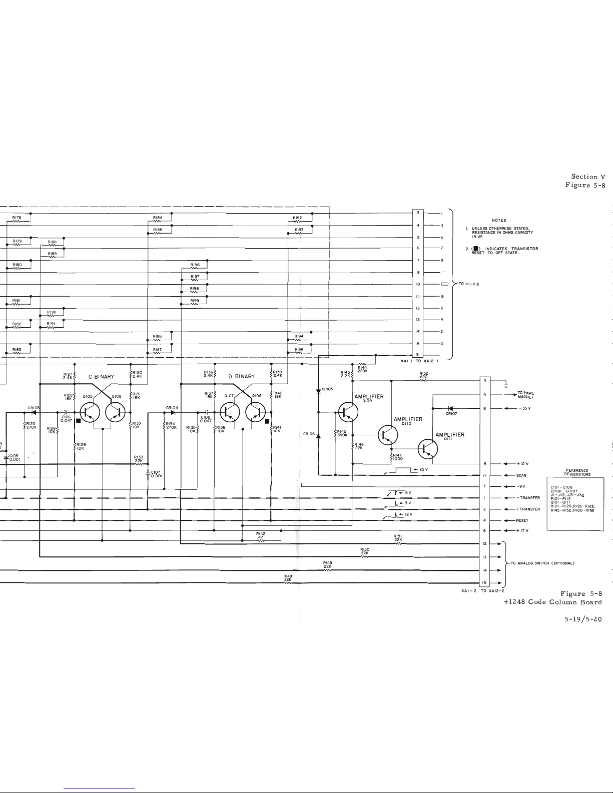
Section
V
Figure
5-8
REFERENCE
DESIGNATORS
C101-C108
CRIOI -
CRI07
JI-JI2,J21-J32
P101-P112
0101-0111
RI01-RI20,RI26-RI43,
R145-R152,
RI60
-R195
TO
ANALOG
SWITCH
(OPTIONAL)
TRANSISTOR
ATE.
E
STATED,
S,CAPACITY
+---
-35
V
+---
- TRANSFER
----+
TO
PAWL
MAGNET
+---+
TRANSFER
+---SCAN
+---
-9V
+---RESET
+---+17V
~+IOV
---~--------------------------I
-
......
T
T
T
:
3
~I
RI78
RI84
RI92
NOTES
1
T
I
4
~3
UNLESS OTHERWIS
RI85
RI93
I.
RESISTANCEINOHM
5
~5
IN
UF.
RI79
T
RI88
T
i
6
1---7
2.
(.l
T
INDICATES
RI89
I
RESETTOOFF
ST
1
T
7
~9
RI80
RI96
8
1----
RI97
T
I I
10
-CJ
TO
PI-PI2
RI98
T
I
:
T
T
I
II
-8
RI81
RI99
12
-6
RI90
T
I
13
-4
RI82
T
RI91
T
I
T
T
14
-2
RI86
RI94
15
-0
RI83
T
RI87
T
RI95
T
I
9
-----
-
-----
---
--
--------------
------
---------------
----
~~
T
-
XAI-ITOXAI2-1
RI44
RI30
RI36
RI39
R145~
220K
RI52
RI27
C BINARY
2.4K
2.4K
D BINARY
2.4K
2.2K
2.4K
820
....-----
-
3
~
RI31
RI37
RI40
I
..
,. CRI05
RI28
0107
0108
-
AMPLIFIER
9
r---
0105
0106
18K
18K 18K
18K
0109
C~~3
CR~~4
I ....
8
to--
"
II
,
......
I
.....
,
II""l
"
~
CRI07
CI06
CI08
AMPLIFIER
0.047
•
0.047
•
RI20
RI32
RI34
0110
270K
RI26
10K
270K
RI35
RI38
RI41
10K
10K 10K
10K
RI43
CRI06~~
390K
~
AMPLIFIER
0111
3
RI29
I
RI46
(
10K
22K
....-l
..
::~gg81
RI33
RI47
22K
1000
5
-
;~gl.gbl
~25V
,
II
-
I
I
7
-
~5V
I
I
-
~3V
,
2
~
~12V
,
4
~
6
-
RI42
I
47
RI51
22K
--.."'"
12
RI50
t
22K
I
13
--..
RI49
>-
22K
14
----..
RI48
22K
--..
I
15
-
./
XAI-2TOXA12-2
Figure
5-8
+1248
Code
Column
Board
5-19/5-20
Page 39
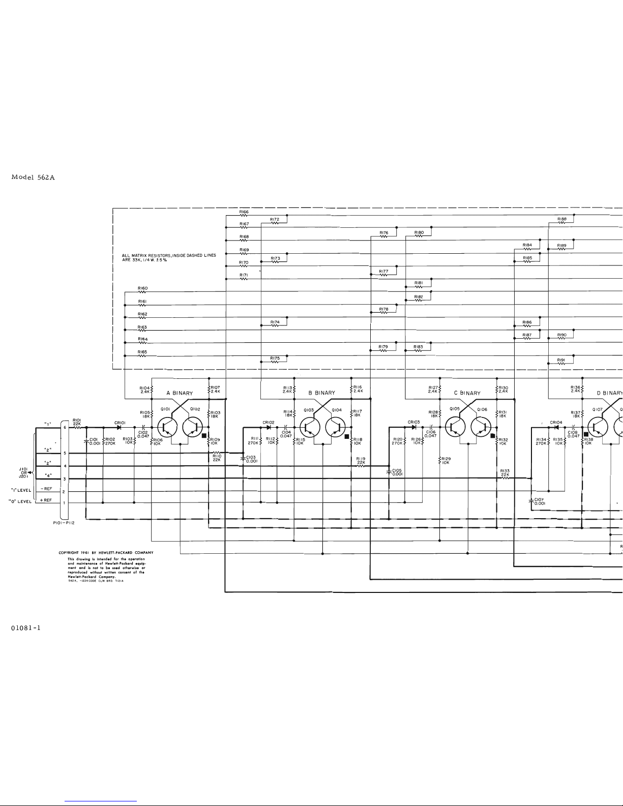
Model
562A
~-------------------------------------------
I
RI66
RI72
I
RI88
I
RI67
RI76
I
RI80
I
RI68
RIB4
I
RIB9
I
RI69
ALL
MATRIX RESISTORS,INSIDE DASHED LINES
RIB
T
RIB5
T
ARE
33K,
1/4W.
±5010
RI70
..
RI77
I
RI71
RI81
T
RI60
RIB2
I
RI61
RI7B
T
RI62
RI74
T
RIB6
T
RI63
RIB7
T
RI90
I
RI64
RI79
T
RI83
T
RI65
RI75
T
RI91
T
L
1----
--
--------
--
----
-------
~--
------
--
---------
------
--
----------
--------,-
------
-------------
. -
RI04
RI07
RI13
RII6
RI27
RI30
RI36
2.4K
ABINARY
2.4K
2.4K
B BINARY
2.4K
2.4K
C BINARY
2.4K
2.4K
DBINARY
0101
0102
RI14
0103
0104
RI17
0105
0106
RI31
0107
0
RI05
RI03
RI28
RI37
18K
18K
18K
18K
IBK
18K
IBK
r-
RIOI
C~IOI
CRI02
CRI03
CRI04
Ill"
22K
"
...
,
.,
...
1
.,
I
.....
I'
6
p
CI102
...
d04
..
1\
~
1\
•
CI06
CIOB
•
0.047
0.047
•
0.047
•
0.047
.,
;;~g~gbl
RI02
RI03
RI06
RI09
Rill
RI12
RI15
RIIB
RI20
RI26
RI32
RI34
RI35
RI3B
-.
270K
10K
10K
10K
270K
10K
10K
10K
270K
10K
10K
270K
10K
10K
"2"
5
RIIO
;;
~g~g51
RI19
RI29
","
22K
22K
10K
4
I+<
;;
,g~851
RI33
t
"4"
22K
3
L
-REF
2
L
+REF
1
*g~gbl
'--
P101-P112
~
R
COPYRIGHT
1961
BY
HEWlm·PACKARD
COMPANY
This
drawingisintended
For
the
operation
and
maintenance
of Hewlett-Packard equip-
ment
andIsnot tobeu.ed otherwi.e or
reproduced without written con.ent of
the
Hewlett-Packard Company.
562A,
-1224CODE
CLlI!.
BRO. T121A
J 10
OR
J20
"I"LEVE
"0"
LEVE
01081-1
Page 40

Section
V
Figure
5-9
REFERENCE
DESIGNATORS
STATED,
S,CAPACITY
TO
ANALOG
SWITCH
(OPTIONAL)
RANSISTOR
ATE
---+
TO
PAWL
MAGNET
~-35V
~+IOV
~SCAN
CIOI-Cloe
JI-JI2,J21-J32
~-9V
PIOI-
PI12
0101-0111
~
- TRANSFER
RIOI-
R120, R126-R143
R145-R152,
RIGO-RI95
~
+TRANSFER
CR101-CR107
~RESET
~+17V
----------------------------I--l
r---
""
\
3
I
RI88
J
I
NOTE
I
4
3
T
I
I
I.
UNLESS
OTHERWISE
RI76
RI80
RESISTANCEINOHM
5
5
IN
UFo
I
I
I
I
2.(.)
INDICATES T
RI84
RI89
6
7
RESET
TO
OFF
ST
RI85
I
:
7
9
RI77
1
RI92
T
i
8
-
RI81
T
RI93
I
!
10
CJ
TO
PI-PI2
RI82
I
RI94
T
:
II
8
RI78
T
RI95
T
i
12
6
RI86
T
I
.
13
4
RI87
T
RI90
I
l
14
2
RI79
T
RI83
T
i
15
0
RI91
T
I
I
9
.-
1-------
-
----------_.-
------
--
--
--
----------
-_.-
1--'---
I-----'
.-
"----
XAI-ITOXAI2-1
r---
RI27
RI30
RI36
RI39
3
~
2.4K
C
BINARY
2.4K
2.4K
D BI NARY
2.4K
RI44
RI51
2.2K
820
-
~'CRI05
9
-
0105
0106
0107
0108
RI40
AMPLIFIER
RI28
RI31
RI37
18K
18K
18K
18K
I
f?
0109
CRI03
I
CRI04
CR~7
...
I'
....
II'
8
-
...
d06
~
"
,
....
CI08
•
AMPLIFIER
0.047
•
0.047
RI20
RI26
RI32
RI34
RI35
RI38
RI41
RI43
0110
270K
10K
10K
270K
10K
10K
10K
390K
CRI06
r-
AMPLIFIER
~~
t?
0111
9
RI29
K
10K
;~g~8gl
RI33
RI45
22K
RI46
22K
1000
5
I---
~5V
~
II
I---
*g~gbl
7
to--
~V
I
I---
~V
~
2
~
4
-
~2V
I
6
-
RI42
RI50
47
22K
~""
12
RI49
22K
~
13
RI48
>
22K
f-----.
14
RI47
22K
15
-----.
""
'--
XAI-2TOXA12-2
Figure
5-9
-1224
Code
Column
Board
5-21/5-22
Page 41
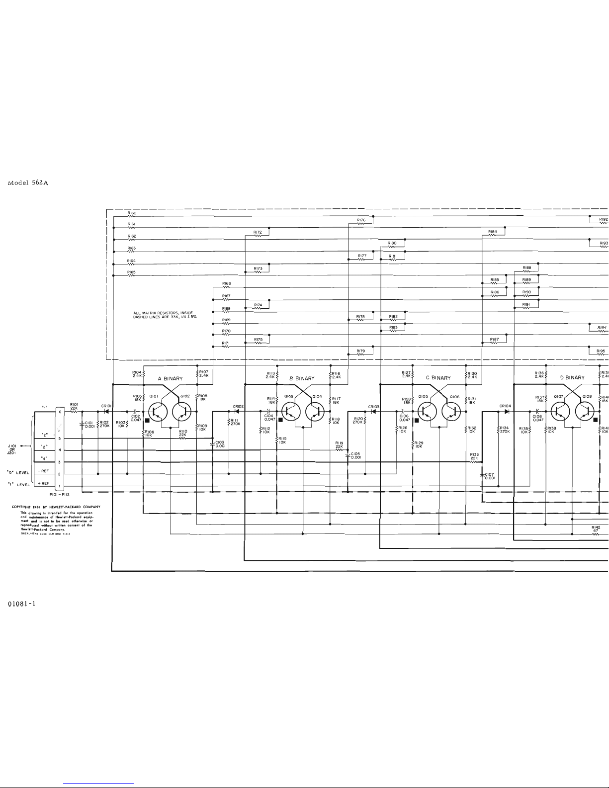
lY10del
562A
r-------------------------------------------------------.
I
RI60
RI76
T
T
RI92
RI61
RI72
T
RI84
T
RI62
RI80
T
T
RI93
,:?163
RI77
T
RI81
I
RI64
RI73
T
RI88
T
RI65
RI85
T
RI89
T
RI66
RI86
T
RI90
T
RI67
RI74
T
RI91
T
RI68
ALL
MATRIX RESISTORS, INSIDE
T
T
DASHED
LINES
ARE
33K,
1/4 ±
5%
RI78
RI82
RI69
-
RI83
T
T
RI94
RI70
RI75
1
RI87
1
RI71
RI79
T
T
RI95
L
~---------------
1-----
1---------------
----
1---------------
----
-------------
RI04
RI07
RI13 RI16
RI27
RI30
RI36
R13!
2.4K
A BINARY
2.4K
2.4K
BBINARY
2.4K
2.4K
C BINARY
2.4K
2.4K
D BINARY
2.41
RI05
0101
0102
RI08
0103
0104
RII7
0105
0106
RI31
RI37
)-
0107 0108
RI41
18K
18K
RII4
RI28
18K
)-
18K
18K
18K
18K
18K
-
RIOI
CRIOI
~R~02
CRI03
CRI04
"I"
22K
I
...
"
"
...
,
..
,
I'
6
-.
....
71
T""It
7r
f"'IIII
/I
"'1
1\
CI02
CI04
RI20
CI06
CIOS
0.047
•
Rill
0.047
•
RII8
0.047
•
0.047
•
~~g~gbl
RI02
RI03
270K
10K
270K
270K
10K
RI09
RI26
RI32 RI34
RI35
RI38
RI41
10K
RII2
...
RI06
RIIO
10K
10K 10K
270K
10K
10K
10K
tl
2
"
10K
22K
5
RII5
.....
~CI03
10K
RI19
RI29
----<
"2"
..;;
0.001
??K
10K
4
I
~~g~g61
RI33
"4"
22K
3
EVEL
- REF
;;~g~g~1
2
EVEL
+REF
I
'---
PIOI-
PII2
RIGHT
1961
IY
HEWLETT
.I'ACKARD
COMPANY
Thil drawingilintended for
the
operation
and
maintenance
of Hewlett·Packard equip.
ment
andilnottobe
uled otherwile
or
reproduced without written
con
lentofthe
RI42
Hewlett·Packard Company.
47
562A,+1224
CODE
ClM
BRD T121A
COI'Y
J
101
OR
J201
01081-1
Page 42

Section
V
Figure
5-10
REFERENCE
DESIGNATORS
CIOI-
cloe
JI-JI2,J21-J32
P101-P1I2
QIOI-OIII
RIOI-
R120,
RI26-RI43.
RI45-RI52,
R160-R195
CR101-CR107
NSISTOR
E.
ATED,
APACITY
TO
ALOG
SWITCH
OPTIONAL)
TO
PAWL
MAGNET
+IOV
-9V
-TRANSFER
SCAN
-35V
RESET
+TRANSFER
+17V
r----
.....
NOTES
T
T
3
~I
RI76
RI92
II
I.
UNLESS OTHERWISE
ST
"
4
fo-3
RESISTANCEINOHMS,C
T
\
T
:
IN
Ufo
RI72
RI84
2.
( )
INDICATES TRA
T T
i
5
-------
5
RESETTOOFF
STAT
RI80
RI93
-7
T T
!
6
RI77
RI81
7
-9
RI73
1
RI88
T
l
8
--
~
T T
RI85
RI89
I
10
-0
>TOPI-PI2
RI86
1
RI90
1
f:
II
-8
RI74
T
RI91
T
'i
T T
"
12
-6
RI78
RI82
13
fo-4
RI83
T
T
RI94
II
14
~2
RI75
r
RI87
1
I
T
T RI95
J
15
~o
RI79
9
~
-------------
----
------------
----
-----------_.-
'---
.."I
RI45
XAI-ITOXAI2-1
RI13
~R116
RI27
RI30
RI36
RI39
2.2K
-
2.4K
B BI NARY
>2.4K
2.4K
C BINARY
2.4K
2.4K
D
BINARY
2.4K
3
-4:-
RI52
820
~~
CRI05
9
RI14
0103
0104
RI17
0105
0106
RI31
RI37
0107 0108
RI40
AMPLIFIER
RI28
18K
18K
18K
18K
18K
18K
tV
0109
CRI03
CRI04
,
...
,
~I
If
,
...
81----
.II
I
....
.II
....
,
1\
~
,
.....
CI04
R120-
CI06
CI08
AMPLIFIER
CRI07
0.047
•
RII8
0.047
•
0.047
•
10K
270K
/
fV'
0110
RII2
RI26
RI32
RI34
RI35
RI38
RI41
RI43
10K
'"
10K
10K
270K
10K
10K
10K
390K
CRI06~~
AMPLIFIER
RII5
W
0111
10K
RII9
RI29
RI46
22K
10K
22K
'~g~g61
RI33
:
RI47
22K
~
1000
5
--
~5V
"
II
--
;;1r-gg61
7--
~V
1--
~V
"
2
--
~2V
,
4
--
6
--
RI42
I
47
RI51
I
22K
....
I
12
r--
RI50
13
r---
RI49
22K
22K
14
f----
~
AN
RI48
(
22K
15
r---
-
XAI-2TOXA12-2
Figure
5-10
+1224
Code
Column
Board
5-23/5-24
Page 43

,..-------------WARRANTY-----------~
All
our products are warranted against defects in materials and workmanship for one year from
the date
of
shipment. Our obligationislimited to repairing or replacing products (except tubes)
which prove to be defective during the warranty period. We are not liable for consequential
damages.
For assistance of any kind, including help with instruments under warranty, contact your authorized
~
Sales Representative for instructions. Give full details of. the difficulty and include the instrument model
and serial numbers. Service data
or
shipping instructions will be promptly sent to you. There will be
no
charge for repair of instruments under warranty, except transportation charges. Estimates of charges for
non-warranty or other service work will always
be
supplied,ifrequested, before work .begins.
CLAIM
FOR
DAMAGE IN SHIPMENT
Your instrument should be inspected and tested as soon as it is received. The instrument is insured for
safe delivery.
If
the instrument is damaged in any wayorfails to operate properly, file a claim with the
carrier or,
if
insured separately, with the insurance company.
SHIPPING
On
receipt of shipping instructions, forward the instrument prepaidtothe destination indicated. You may
use the original shipping carton
or
any strong container. Wrap the instrument in heavy paper or a plastic
bag and surround it with three
or
four inches of shock-absorbing material to cushion it firmly and prevent
movement inside the container.
GENERAL
Your authorized~Sales Representativeisready to assist you in any situation, and you are always
wel-
come to get directly in touch with Hewlett-Packard service departments:
00390-1
CUSTOMER SERVICE
Hewlett-Packard Company
395
Page
Mill
Road
Palo
Alto.
California,
U.S.A.
Telephone: DAvenport
6-1755
Direct
Dial
Area Code
415
TWX
No.
PALAL117-U
Cable: "HEWPACK"
OR (In Western Europe)
Hewlett-Packard
S.A.
RueduVieux
Billard
No.1
Geneva.
Switzerland
Telephone:
(022)
26.
43.
36
Cable:
"HEWPACKSA"
Page 44

r!jJ
MANUAL
CHANGES
MODEL 562A
DIGITAL RECORDER
Serials
Prefixed:
134-
Manual
Printed:
9/61
The following
changes
adapt
this
manualtoinstruments
having the
serial
prefixes
listed
below:
(Ch.
=If
= Change Number; Sere
Pre.
=
Serial
Prefix)
Ch.
=If
Ser.
Pre.
New
Data
.1
,.
1
2
3
4
134-
134-
134-
134-
On
the Column
Board
schematics,
The
scan
signal
should be a negative going25volt
signal.
Resistors
RI06,
109, 115, 118, 129, 132, 138, and 141 have been changed to
4.7K.
Change R142to22
ohms.
On
the
Control
Board,
(Figure
5-5)
R221 should
read
68 oluns.
R222 should
read
68 oluns.
R279 should
read
560 ohms.
Resistor
R287 should
returntothe
reset
line
instead
of the +17
volt
line.
On
the
Wiring
and
Power
Supply
diagram
(Figure
5-3),
Delete
Fuse
Fl.
FuseFlshouldbein the
line
coming
from
the
upper
half
of the AC
power
plug.
P301 and
302
should have the
reference
voltages
appliedtopins
1 and 2
insteadofpins
3 and
4.
R303 shouldbechangedto100
ohms.
On
the Analog
Circuitry
schematic
(Figure
5-6),
C406:
Capacitor,
0.05
uf,
should be added
from
the junction of R433-434 to ground.
Change C406
to
C407.
The 2.
4V
breakdown diode should have the
reference
designator
CR422.
J501: The
wires
from
pins17and18should be
reversed.
Change R40toR409.
Change R49
to
R439.
R349 should
be
changedto1. 8K.
R434 should
be
changedto2. 5K.
R442 should
be
changedto6.8K.
R446:
Resistor,
470 ohms, should be added
from-9V to ground on the analog
board.
Change R415 to R415A and R416toR415B.
Total
resistance
of both
resistorsisfactory
adjusted
to 303K.
Change R417 to R417A and R418 to R417B.
Total
resistance
of both
resistorsisfactory
adjusted
to 606K.
Change R419 to R419A and R420 to R419B.
Total
resistanceofboth
resistorsisfactory
adjusted to 606K.
Change R425 to R425A and R426 to R425B.
Total
resistanceofboth
resistorsisfactory
adjusted
to 1.212 megoluns.
On
all
sectionsofS5,
Change pin
15
to 12,14to
!.t
13 to
!1,
and12to 15.
11/8/61
Page 45
~
Manual Changes Model
562A
Page
2
Ch.
# Sere
Pre.
New
Data
5 134- Addition to text:
At the
rear
of the
recorder,
an
interlock
switch, S2,
has
been installed. When the
back
of
the
recorderisremoved, fan
motorB1stops.
6 147-
This
manual
applies
with the above changes.
•
12/15/61 -
5G2A
11/8/61
562A
Page 46
,
OPERATING
AND
SERVICING
MANUAL
FOR
SPECIFIC
TION
H19-562A/AR
DIGIT L RECORDER
Specific
tion
H19,
>562
I
is
simi!
r to
the
s nd r
odel
562 /
AR
Digit: I
Recor
eroThis
speci1instrument
has
be
n nlodifi s followso
1
0
The
twelfth
column
cover
in
the
Oper
ting
nd
Service
M
nual
for
the
562/AR
has
been ed
to
this
instrument
o
20SpeciIprint
wheelshve
been
ins
led
in
columns
eight
n
nine
o
The
columns
re
numbered
from
ri
ht
to
ef
when f
cing
front
of
the
instrumen
0
The
ch
r
cters
on
th
print
wheel
re
shown in
the
followi
ble
Ion with s nd r
wheel
for
ref
renc
purposes
o
PRI
T
WHEEL
CHAR CTERS
13579
-
86420
3579
+86420
CEGI
KLHFDBJ
13579
-
86420
COLUMN
NUMBER
~STOCK
NUMB
562
-95B
562
-83E
-1713
562 =83E 1707
562
-95B
Encl:
562A
PrintoMech
o
1 c
mn
m 362
HEWLETT-PACKARD
COMPANY 1501
PAGE
M~L
ROAD
PALO
ALTO
CALIF.
U.S.A.
Page 47
SP CI L
AR
S
'OR
12-C
LU
. I T
.t.C
I M -
The
following
chan
es
ve
been
made i
the
t
lYe-col
n
printer
mechanism
in
this
special
in
rument.
These
chan
es
apply
to
the
Re
aceable
Iarts
Tables
and
their
associated
'
illustrations
in
th
Operating
and
Service
Manual
for
the
Printer
echanism.
Fa e
5-10
1
2
3
thru
10
11
12
14
D
Wheel
bank,
complete
t,
pri
t
heel
shaft
No
cha
~e
in
description
or
Stock
No.;
increase
uantity
to
t
elve.
Shaft
print
wheel
as
er,
shouldered
asher,
s
ring
retaini
g
(p
STOCK
NO.
t
Special
561A-57A
561
-37B
561 -8aA
561A-88B
T *
1
1
12
1
1
1
RS*
1
o
o
1
1
Fage
5-12
23
o
cha
ge
in
description
or
Stock
0.;
increase
quantity
to
fourteen.
Fa e
5-14
------
14
Print
bar
56lA-I07A
14
1
2
2
1
1
o
1
o
1
1
1
1
1
12
t
Special
t
pecial
561 -12A
561 -107B
t P
cial
2
3
4
7
5, 6
Fage
5-20
1
wI
agnet
assembly,
com
lete
Ma
net
adjust
plate
Iawl-
older
bar
awl
assembly
(rivited
assembly
includi
g
flat
spring,
12
armatures,
and
12
pa
Is).
o
change
n
description
or
Stock
0.;
increase
quantity
to
twelve.
agne
frame
subassembly
(includes
yokes
and
cores)
· t
Special
items
do
not
have
an
~stock
number.
To
obtai
replacements,
order
by
description
and
instrum
nt
model
number.
•
See
introduction
to
SieTrON
V
in
he
0
eratin
and
Service
anual
for
the
Prin
ec
anism.
l,.
Page 48

 Loading...