

Page 1

Errata
Title & Document Type: HP5501B Laser Head Operating & Service Manual
Manual Part Number: 05501-90035
Serial Prefixes: 2632
Revision Date: September 1986
HP References in this Manual
This manual may contain references to HP or Hewlett-Packard. Please note that HewlettPackard's former test and measurement, semiconductor products and chemical analysis
businesses are now part of Agilent Technologies.
Changes to this Manual
No changes have been made to this manual, with the exception of correcting the odd
spelling and grammatical errors. In some places original photographs may be replaced
or augmented with modern digital photographs. (it’s weird looking at an old BW HP
manual and seeing a color photograph… still gets me)
About this Manual
This manual is reproduced from high-resolution scans of an original document, which
was then converted to Word format using custom designed OCR software for my
personal use.
This means that what you see here is not a scan of a scan/copy.
OCR errors may exist and as such the user of this document should take care and use
common sense when referencing this documentation.
Copyright Notice
This documentation is © Copyright 1980 Hewlett Packard and © Copyright 2006, Jack Hudler,
hpdocs@hudler.org.
Permission to use and redistribute this documentation for non-commercial and internal corporate
purposes is hereby granted, free of charge.
Any redistribution of this documentation or its derivates must include this copyright notice.
You may not sell this documentation or its derivations without written consent.
You may modify this documentation as necessary, but you may not sell derivative works based
on it.
You may include this documentation with the equipment/hardware on which it is used for the
purposes of selling the equipment/hardware. If you advertise that a copy of this documentation is
included in the sale, you must state that is for “Free”.
Meaning if you want to gratuitously toss in a copy of the manual on an eBay sale, it’s ok with me
as long as you state it’s for free. No you can’t sell a digital archive of manuals and say it includes
a free copy of this documentation. You must give it away with equipment.
I think you get the spirit of the copyright; it takes a lot of hours to scan and replicate a manual. I
just want this used in the spirit in which is it given.
Agilent if you have questions or wish to include this in your archive email me.
Page 2
ii
Page 3

OPERATING AND SERVICE MANUAL
HP5501B
LASER HEAD
SERIAL NUMBER PREFIX: 2632A
This manual applies directly to HP5501B Laser Heads
with serial numbers prefixed 2632A. Lower number serial
prefixes are covered in Section 7 while higher number
serial prefixes are documented with "Manual Changes"
Supplements described in Section 7.
© HEWLETT-PACKARD COMPANY 1986
5301 Stevens Creek Blvd., Santa Clara, CA 95051-7299
Portions © by Jack Hudler 2006
hpdocs@hudler.org
MANUAL PART NUMBER 05501-90035
Microfiche Part Number 05501-90036 Printed: SEPTEMBER 1986
Page 4
ELECTRICAL SAFETY CONSIDERATIONS
GENERAL
The product and related documentation must be reviewed for
familiarization with safety markings and instructions before
operation.
This product is a Safety Class I instrument (provided with a
protective earth terminal).
BEFORE APPLYING POWER
Verify that the product is set to match the available line voltage
and the correct fuse is installed. Refer to
Section 2, Installation.
SAFETY EARTH GROUND
An uninterruptible safety earth ground must be provided from
the main power source to the product input wiring terminals,
power cord, or supplied power cord set.
SAFETY SYMBOLS
Instruction manual symbol: the product
will be marked with this symbol when it
is necessary for the user to refer to the
instruction manual.
Indicates hazardous voltages.
Indicates earth (ground) terminal.
The WARNING sign denotes a hazard. It
calls attention to a procedure, practice,
or the like, which, if not correctly
performed or adhered to, could result in
personal injury. Do not proceed beyond
a WARNING sign until the indicated
conditions are fully understood and met.
LASER HEAD SAFETY CONSIDERATIONS
The CAUTION sign denotes a
hazard. It calls attention to an
operating procedure, practice, or the
like, which, if not correctly performed
or adhered to, could result in
damage to or destruction of part or
the entire product. Do not continue
beyond a CAUTION sign until the
indicated conditions are fully
understood and met.
Any interruption of the protective (grounding) conductor (inside
or outside the instrument) or disconnecting the protective earth
terminal will cause a potential shock hazard that could result in
personal Injury. (Grounding one conductor of a two conductor
outlet is not sufficient protection).
Whenever it is likely that the protection has been impaired, the
instrument must be made inoperative and be secured against
any unintended operation.
If this instrument is to be energized via an autotransformer (for
voltage reduction) you must make sure the common terminal is
connected to the neutral (earthed pole) of the power source.
Servicing instructions are for use by service-trained personnel
only. To avoid dangerous electric shock, do not perform any
servicing unless qualified to do so.
Adjustments described in the manual are performed with power
supplied to the instrument while protective covers are removed.
Energy available at many points may, if contacted, result in
personal injury.
Capacitors inside the instrument may still be charged even if the
instrument has been disconnected from its source of supply.
For continued protection against the fire hazard, replace the line
fuse(s) only with 125V fuse(s) of the same current rating and
type (for example, normal blow, time delay, etc.). Do not use
repaired fuses or short circuited fuse holders.
From 1.2 kilovolts to 12 kilovolts dc is present on the anode of
the laser tube in the 5501B. Exercise extreme caution when
working inside the instrument. The high voltage could cause
serious personal injury if contacted. Any adjustments performed
should be by service trained personnel only.
LASER RADIATION IS EMITTED FROM THE APERTURE ON THE 5501B LASER HEAD AS
ILLUSTRATED ON THE FOLLOWING PAGE. DO NOT STARE INTO BEAM. THIS PRODUCT IS A
CLASS II LASER PRODUCT CONFORMING TO U.S. NATIONAL CENTER FOR DEVICES AND
RADIOLOGICAL HEALTH REGULATIONS 21 CFR 1040.10 AND 1040.11. THE MAXIMUM RADIANT
POWER OUTPUT IS 1 MILLIWATT, THE PULSE SPECIFICATION IS CONTINUOUS WAVE, THE
LASER MEDIUM IS HELIUM-NEON, AND THE WAVELENGTH IS 632.991 NANOMETRES.
LASER RADIATION IS ACCESSIBLE WHEN THE 5501B COVERS ARE REMOVED AND THE TESTNORM SWITCH, A1S2, IS IN THE TEST POSITION.
USE OF CONTROLS OR ADJUSTMENTS OR PERFORMANCE OF PROCEDURES OTHER THAN
THOSE SPECIFIED HEREIN MAY RESULT IN HAZARDOUS RADIATION EXPOSURE.
ii
Page 5
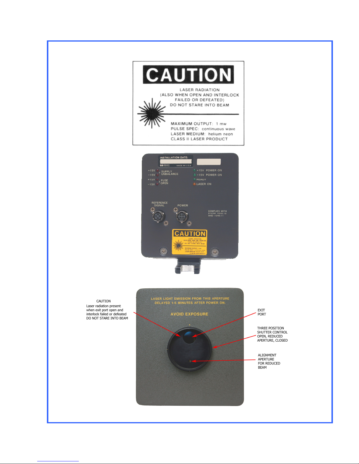
LASER HEAD SAFETY LABELS
iii
Page 6

END PRODUCT LASER SAFETY
CONSIDERATIONS
The 5501B Laser Head complies with U.S. National Center for
Devices and Radiological Health regulations 21 CFR 1040.10 and
1040.11.
These regulations may also apply to the end product into which
the 5501B will be designed. Care must be taken to insure that the
end product complies with all applicable national and local laser
safety regulations.
iv
Page 7

Table of Contents
1 GENERAL INFORMATION ...................................................................................................................1-2
1-1. Introduction..............................................................................................................................1-2
1-4. Equipment Description ............................................................................................................1-2
1-8. Manual Organization................................................................................................................1-3
1-10. Instruments covered by this manual........................................................................................1-3
1-14. Safety Considerations..............................................................................................................1-4
1-16. Equipment Supplied ................................................................................................................1-4
1-18. Available Accessories ..............................................................................................................1-4
1-20. Specifications...........................................................................................................................1-5
1-22. Recommended Test Equipment..............................................................................................1-6
1-24. Warranty...................................................................................................................................1-6
2 INSTALLATION.....................................................................................................................................2-1
2-1. Introduction..............................................................................................................................2-1
2-3. Unpacking, Inspection, and Reshipment.................................................................................2-1
2-5. Unpacking and Inspection.......................................................................................................2-1
2-7. Warranty Claims.......................................................................................................................2-1
2-9. Laser Tube Shipment...............................................................................................................2-1
2-11. Tagging for Service..................................................................................................................2-2
2-13. Packaging for Reshipment.......................................................................................................2-2
2-14. Installation ................................................................................................................................2-2
2-16. System Cabling........................................................................................................................2-2
2-19. Power and Signal Connections................................................................................................2-5
2-21. Cable Fabrication.....................................................................................................................2-5
2-23. Grounding Considerations.......................................................................................................2-7
2-25. Power Supply Requirements ...................................................................................................2-7
2-27. Power Dissipation ....................................................................................................................2-7
2-29. Fusing.......................................................................................................................................2-7
2-31. Dimensions ..............................................................................................................................2-8
2-33. Mounting and Fixturing............................................................................................................2-9
3 OPERATION.......................................................................................................................................3-10
3-1. Introduction............................................................................................................................3-10
3-4. Power Application ..................................................................................................................3-10
3-6. HP5501B Laser Head Front Panel Controls ..........................................................................3-10
3-8. HP5501B LASER HEAD REAR PANEL INDICATORS AND CONNECTORS.........................3-11
3-10. OPERATING MODES.............................................................................................................3-13
3-12. Warmup Time Operating Notes .............................................................................................3-14
3-13. HP 10740A Coupler Based Systems - Manual Monitoring....................................................3-14
3-14. Systems with HP10745A or HP10746A Cards - Automatic Monitoring.................................3-14
3-16. HP10740A Coupler - Error Signal Information.......................................................................3-14
3-17. HP10746A Error Signal Processing.......................................................................................3-15
3-18. HP 10745A Background Information .....................................................................................3-15
3-19. Program Modifications...........................................................................................................3-15
4 PERFORMANCE TESTS ......................................................................................................................4-1
4-1. Introduction..............................................................................................................................4-1
4-3. RECOMMENDED TEST EQUIPMENT .....................................................................................4-1
4-5. TEST RECORD.........................................................................................................................4-1
4-7. HP5501B PERFORMANCE TEST ............................................................................................4-1
4-9. Input Voltage Check.................................................................................................................4-1
4-11. Laser Power Output Test .........................................................................................................4-1
4-13. Procedure.................................................................................................................................4-2
v
Page 8

Table of Contents
5 ADJUSTMENTS....................................................................................................................................5-1
5-1. Introduction ..............................................................................................................................5-1
5-3. Safety Considerations..............................................................................................................5-1
5-5. Recommended test equipment ...............................................................................................5-1
5-7. Factory Selected Components ................................................................................................5-1
5-9. Adjustment Procedures............................................................................................................5-2
5-11. Reference Temperature Adjustments ......................................................................................5-2
5-14. Preliminary Procedure..............................................................................................................5-2
5-17. Laser Tube Current Adjustment...............................................................................................5-4
6 REPLACEABLE PARTS........................................................................................................................6-1
6-1. Introduction ..............................................................................................................................6-1
6-4. Exchange Assemblies..............................................................................................................6-1
6-6. ABBREVIATIONS AND REFERENCE DESIGNATIONS...........................................................6-1
6-8. ORDERING INFORMATION .....................................................................................................6-1
6-11. DIRECT MAIL ORDER SYSTEM...............................................................................................6-2
6-14. Exploded View........................................................................................................................6-11
7 MANUAL CHANGES ............................................................................................................................7-1
7-1. Introduction ..............................................................................................................................7-1
7-3. Newer Instruments ...................................................................................................................7-1
8 SERVICE ..............................................................................................................................................8-1
8-1. Introduction ..............................................................................................................................8-1
8-3. Theory of Operation .................................................................................................................8-1
8-5. Recommended Test Equipment..............................................................................................8-1
8-7. Service Aids..............................................................................................................................8-1
8-9. Schematic Diagram Symbols and Reference Designations....................................................8-1
8-12. Safety Considerations..............................................................................................................8-3
8-14. Safety Symbols ........................................................................................................................8-4
8-16. Before and After Service Product Safety Checks ....................................................................8-5
8-18. LASER HEAD BLOCK DIAGRAM DESCRIPTION ....................................................................8-5
8-26. Laser Tuning ............................................................................................................................8-7
8-29. Warmup Mode Tuning .............................................................................................................8-7
8-34. Optical Mode Tuning................................................................................................................8-9
8-40. Laser Assembly Optics ..........................................................................................................8-12
8-42. Reference Receiver ................................................................................................................8-12
8-44. Shutter Mechanism ................................................................................................................8-12
8-46. ASSEMBLY/SCHEMATIC LOCATIONS OF HP5501B BLOCK DIAGRAM ELEMENTS.........8-12
8-47. REAR PANEL LED INDICATORS ...........................................................................................8-12
8-52. ASSEMBLY REMOVAL INSTRUCTIONS ...............................................................................8-14
8-62. TROUBLE ISOLATION ...........................................................................................................8-19
8-63. Quick Tuning Checkout Procedure .......................................................................................8-19
8-67. Testing the Liquid Crystal Switch...........................................................................................8-21
8-70. HP5501B Trouble Isolation Procedures.................................................................................8-23
8-72. Procedure...............................................................................................................................8-24
8-73. A1 CONNECTOR BOARD CIRCUIT THEORY........................................................................8-26
8-76. High Voltage Power Supply Switch (A1Q3 and A1Q4)..........................................................8-26
8-79. Power Distribution..................................................................................................................8-26
8-83. A1 CONNECTOR BOARD TROUBLESHOOTING..................................................................8-27
8-85. Rear Panel LED Operational Check.......................................................................................8-27
8-87. A2 HIGH VOLTAGE POWER SUPPLY CIRCUIT THEORY.....................................................8-29
8-89. HIGH VOLTAGE POWER SUPPLY TROUBLESHOOTING....................................................8-29
8-91. A3 CONTROLLER/REFERENCE BOARD AND A4 SAMPLER BOARD CIRCUIT THEORY...8-32
8-92. Introduction ............................................................................................................................8-32
8-95. Clock Ⓐ..................................................................................................................................8-32
vi
Page 9

Table of Contents
8-97. Dividers Ⓑ..............................................................................................................................8-32
8-99. State Machine Ⓕ....................................................................................................................8-33
8-105. Liquid Crystal Ⓓ .....................................................................................................................8-34
8-109. Photodiode and Amplifier Ⓔ..................................................................................................8-34
8-111. Warmup Error Amplifier and Comparator Ⓙ .........................................................................8-34
8-114. Subtracting Sample and Hold Ⓗ ...........................................................................................8-34
8-118. A1/A3 Power Amplifier Ⓘ .......................................................................................................8-35
8-121. Reference Receiver Ⓛ ...........................................................................................................8-36
8-125. Line Driver Ⓚ..........................................................................................................................8-36
8-127. Power-On Reset (POR) Ⓖ......................................................................................................8-36
8-129. Laser Head Power Ⓒ .............................................................................................................8-36
8-131. A4 Sampler Board..................................................................................................................8-36
8-133. A3 CONTROLLER/REFERENCE BOARD TROUBLESHOOTING..........................................8-37
8-135. Standard Troubleshooting Procedures .................................................................................8-37
8-137. Digital Troubleshooting..........................................................................................................8-38
8-140. Photodiode and Amplifier Troubleshooting...........................................................................8-41
8-142. Liquid Crystal Troubleshooting..............................................................................................8-42
8-144. Subtracting Sample and Hold Troubleshooting ....................................................................8-42
8-146. Power Amplifier Troubleshooting...........................................................................................8-44
8-148. Warm-Up Error Amplifier Troubleshooting ............................................................................8-46
8-150. Power Supply Troubleshooting .............................................................................................8-46
8-152. Reference Receiver Troubleshooting.....................................................................................8-47
9 SERVICE NOTES .................................................................................................................................9-1
9-1. Service Note 5501-02A July 2001............................................................................................9-1
vii
Page 10

List of Figures
Figure 1-1 HP5501B Laser Head..................................................................................................................1-1
Figure 2-1. HP 107788 Power Cable ............................................................................................................2-3
Figure 2-2. HP 107798 Reference Cable......................................................................................................2-4
Figure 2-3. Typical Transducer System Interconnections............................................................................2-5
Figure 2-4. Interconnecting Plug Details ......................................................................................................2-5
Figure 2-5. HP 5501B Laser Head Interconnect Wire Fabrication ...............................................................2-6
Figure 2-6. Mounting Details and Physical Characteristics..........................................................................2-8
Figure 3-1. HP5501B Front Panel Controls ................................................................................................3-10
Figure 3-2. HP5501B Rear Panel Connectors and Indicators....................................................................3-11
Figure 3-2. HP5501B Rear Panel Connectors and Indicators (Continued)................................................3-12
Figure 4-1. HP5501B Power Connection......................................................................................................4-2
Figure 5-1. A 1 Connector Board, TEST-NORM Switch and Adjustment Locations....................................5-2
Figure 5-2. A3 Controller/Ref Board, Jumpers, Test Points, and Adjustment Locations.............................5-3
Figure 5-3. 55018 High Voltage Areas and Anode Lead..............................................................................5-5
Figure 6-1. HP5501B Laser Head Exploded View......................................................................................6-11
Figure 8-1. Schematic Diagram Notes..........................................................................................................8-2
Figure 8-2.HP5501B Laser Head Block Diagram.........................................................................................8-6
Figure 8-3. Flow Diagram for State Machine................................................................................................8-7
Figure 8-4. Feedback Loop during Warmup Mode......................................................................................8-8
Figure 8-5. Warmup Mode Timing Diagram.................................................................................................8-9
Figure 8-6. Feedback Loop During Optical Mode........................................................................................8-9
Figure 8-7. A6 Sampler Assembly, Exploded View....................................................................................8-10
Figure 8-8. Liquid Crystal Timing Diagram (Optical Mode)........................................................................8-11
Figure 8-9. Logic Clip Monitoring of Test IC U9 .........................................................................................8-14
Figure 8-10. HP5501B Front Panel and Side Cover Removal....................................................................8-16
Figure 8-11. Factory-adjusted Sampler Mount (MP1)................................................................................8-18
Figure 8-12. Laser Tube Tuning Characteristics.........................................................................................8-19
Figure 8-13. Quick Tuning Check Test Setup ............................................................................................8-20
Figure 8-14. Quick Tuning Check Waveform Display.................................................................................8-21
Figure 8-15. Liquid Crystal Removal...........................................................................................................8-21
Figure 8-16. Liquid Crystal Test Setup .......................................................................................................8-22
Figure 8-17. HP5501B TEST-NORM Switch A1S2 .....................................................................................8-23
Figure 8-18. High Voltage Power Supply, Schematic Diagram..................................................................8-31
Figure 8-19. State Machine Timing Diagram..............................................................................................8-33
Figure 8-20. Test Point 11 Waveform (HEATER SENSE)...........................................................................8-44
Figure 8-21. E-REF [U20 (Pin 9)]................................................................................................................8-45
Figure 8-22. REFerence Signal Waveforms................................................................................................8-47
Figure 8-23. A1 Connector Board Component Locator .............................................................................8-50
Figure 8-23. A1 Connector Board Component Schematic Diagram..........................................................8-51
Figure 8-23. A1 ↔ A3 Connector Pin Table................................................................................................8-52
Figure 8-24. A3 Controller/Reference Board (05501-60027) and A4 Sampler Board (05501-60029)
Schematic Diagram (Sheet 1 of 2)..............................................................................................................
Figure 8-24. A3 Controller/Reference Board (05501-60027) and A4 Sampler Board (05501-60029)
Schematic Diagram (Sheet 2 of 2)..............................................................................................................
Figure 8-24 A3 Controller/Reference Board and A4 Sampler Board Photos & Data ....................................57
8-55
8-56
viii
Page 11

List of Tables
Table 1-1. HP5501B Laser Head Specifications and Performance Characteristics.....................................1-5
Table 1-2. Recommended Test Equipment..................................................................................................1-6
Table 2-1. Laser Head System Signal Chart.................................................................................................2-6
Table 2-2. HP 5501B Power Supply Requirements......................................................................................2-7
Table 3-1. Proper 55018 Rear Panel LED Power-up Sequence.................................................................3-13
Table 3-1. Program Modifications for Table 4-12 in the HP5501A System Manual ...................................3-16
Table 3-2. Program Modifications for Table 4-13 in the HP5501A System Manual ...................................3-17
Table 3-3. Modified HP10745A HP-IB Interface Program...........................................................................3-18
Table 3-4 Modified HP10746A Binary Interface Program...........................................................................3-19
Table 4-1. Input Voltage................................................................................................................................4-1
Table 6-1. Exchange Assemblies .................................................................................................................6-1
Table 6-2. Reference Designations and Abbreviations ................................................................................6-3
Table 6-3. HP5501B Board Assemblies Replaceable Parts .........................................................................6-4
Table 6-3. HP5501B Board Assemblies Replaceable Parts (Continued).....................................................6-5
Table 6-3. HP5501B Board Assemblies Replaceable Parts (Continued).....................................................6-6
Table 6-3. HP5501B Board Assemblies Replaceable Parts (Continued).....................................................6-7
Table 6-3. HP5501B Board Assemblies Replaceable Parts (Continued).....................................................6-8
Table 6-3. HP5501B Board Assemblies Replaceable Parts (Continued).....................................................6-9
Table 6-3. HP5501B Miscellaneous Chassis Parts (Continued) ................................................................6-10
Table 6-4. Manufacturer's Code List...........................................................................................................6-12
Table 8-1. A3 U9 Test IC Signal Summary.................................................................................................8-13
Table 8-2. DC Unbalanced Failures............................................................................................................8-26
Table 8-3. IC A3U4 and A3U6 Divider Check.............................................................................................8-39
Table 8-4. Signature Table..........................................................................................................................8-41
Table 8-5. Voltage Testpoints and Limits ...................................................................................................8-46
Table 8-6. A3U17 Reference Receiver Test Voltages.................................................................................8-48
ix
Page 12

Page 13
HP5501B
Installation
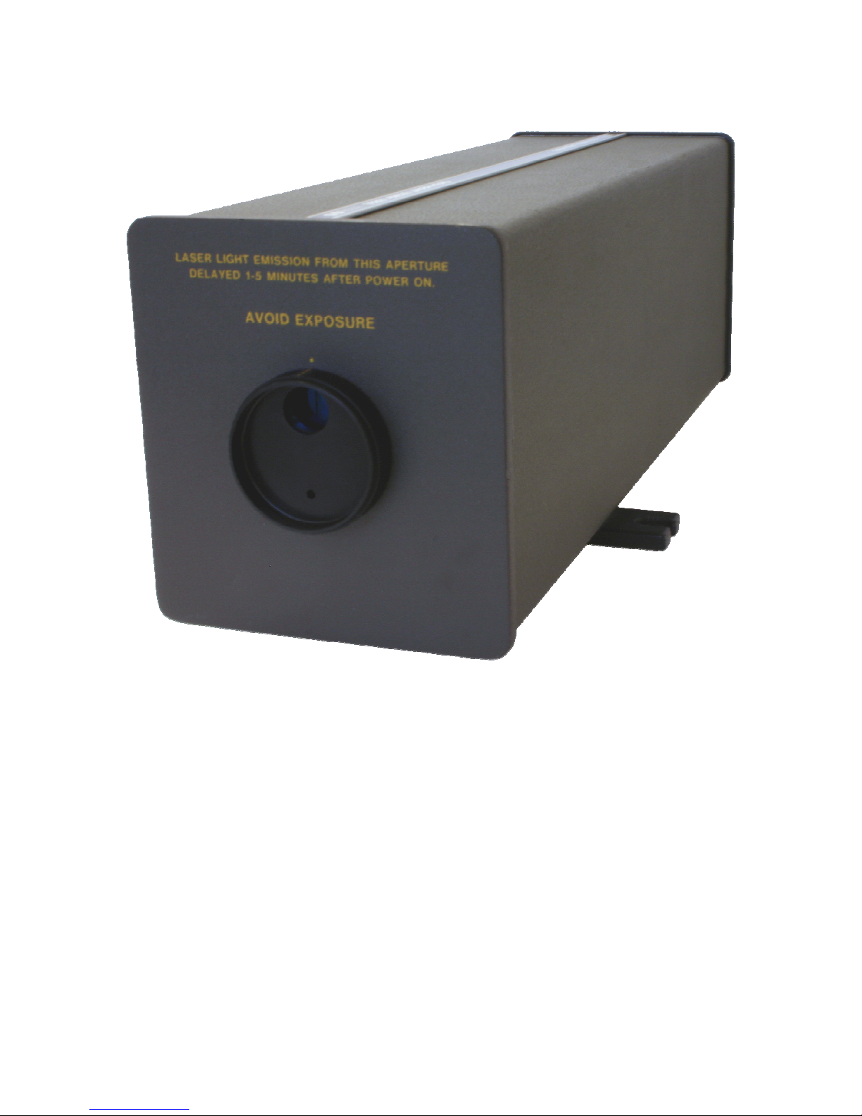
Figure 1-1 HP5501B Laser Head
1-1
Page 14

HP5501B
Installation
1 GENERAL INFORMATION
1-1. Introduction
1-2. This Operating and Service Manual contains information required to install, operate, test, adjust,
and service the Hewlett-Packard Model 5501B Laser Head. The information in this manual is
specific to the HP5501B and supplements other publications available for Hewlett-Packard Laser
Transducer products. Also available is the HP5501A Laser Transducer System Manual (HP Part
Number 05501-90028) that describes how to setup, align, and use the laser system to make
interferometer measurements.
1-3. The HP part number of this manual is listed on the title page. Also listed is a microfiche part
number for ordering 4 X 6" microfilm transparencies of this manual. The microfiche package also
includes the latest "Manual Changes" supplement and any pertinent Service Notes.
1-4. Equipment Description
1-5. The HP5501B Laser Head consists of a thermally-tuned laser tube, control circuits, a reference
receiver, and a high-voltage power supply. The laser head requires ±15 Volt supplies, each with
a minimum capacity of 1 Amp. The HP5501B produces a frequency stabilized laser beam, a
balanced reference output (see paragraph 16), a +15 Volt fused output, and a +5 Volt output.
Diagnostic LED’s, mounted on the 5501B's rear panel, provide status information on power
supply input (±15 Volts), fuses, laser output and tuning, and the reference frequency output.
1-6. The 5501B laser beam consists of two linearly polarized and mutually perpendicular (orthogonal)
components separated in frequency by approximately 1.8 MHz. The two components have light
frequencies of F1 and F2. The higher frequency component (F2) is oriented parallel to the laser
base, while the lower frequency component (F1) is perpendicular to the laser base. An optical
receiver inside the HP5501B detects the 1.8 MHz frequency difference and places it at the rear
panel REFERENCE SIGNAL connector as a balanced output (called the REFerence Frequency).
The reference output is one signal used by the external electronics to measure distance traveled.
1-7. During a typical measurement application, the laser beam travels through external optics where
the horizontal and vertical components of the beam are separated. One component travels along
a fixed path and returns to an external optical receiver. The other component travels along the
path (axis) to be measured and then returns to the external receiver. The external receiver
detects the frequency difference between the two components and outputs a signal called the
MEASure Frequency. The MEASure Frequency from the external receiver and the REFerence
Frequency from the laser head are compared by external, customer selected electronics. If the
distance between the external optics is fixed, the MEASure and REFerence frequencies are
equal. As the relative distance between the external optics changes, the MEASure Frequency
changes due to a Doppler frequency shift. This relative change between the MEASure and
REFerence Frequencies is used by the system electronics to compute distance traveled. The
laser transducer system can be configured for computer control of open- and closed-loop
positioning and measuring applications, having single or multiple axes. For more detailed
information, refer to the HP5501A Laser Transducer System manual (HP Part Number 05501-
90028).
1-2
Page 15

HP5501B
Installation
1-8. Manual Organization
1-9. This Service Manual is organized as follows:
SECTION 1, GENERAL INFORMATION: covers Equipment Description, Manual Organization,
Instruments Covered by this Manual, Safety Considerations, Equipment Supplied, Available
Accessories, Specifications, Recommended Test Equipment, and Warranty Information.
SECTION 2, INSTALLATION: covers Grounding Considerations, Power Requirements, Interconnecting
Cabling, Operating and Storage Environments, Storage and Shipment, and Packaging.
SECTION 3, OPERATION: provides operating information and covers Equipment Front and Rear Panel
Features, Warm-up Time Considerations, and Program Notes.
SECTION 4, PERFORMANCE TESTS: provides Safety Considerations, Performance Tests, and a Test
Record.
SECTION 5, ADJUSTMENTS: covers Safety Considerations, Test Equipment Required, Adjustment
Procedures, and an Adjustment Record.
SECTION 6, REPLACEABLE PARTS: includes Tables of Replaceable Parts including illustrated parts
breakdowns of chassis and mechanical assemblies, Abbreviations, Ordering Information, and
the HP Direct Mail Order System.
SECTION 7, MANUAL CHANGES: describes how to update or backdate the manual for prefixes other
than those listed on the title page.
SECTION 8, SERVICE: contains Safety Considerations, Theory and Block Diagram Descriptions,
Trouble Isolation, Troubleshooting, Schematics, and Component Locations.
1-10. Instruments covered by this manual
1-11. Attached to each instrument is a serial plate. The serial number is in the form: OOOOAOOOOO.
It is in two parts; the first four digits and the letter are the serial number prefix and the last five
digits are the suffix. The prefix is the same for all identical instruments; it changes only when a
change is made to the instrument. The suffix is assigned sequentially and is unique to the
individual instrument. This manual applies to instruments with the serial number prefix listed on
the title page of this manual.
1-12. An instrument manufactured after the printing of this manual may have a serial number prefix
that is not listed on the title page. This unlisted serial number prefix indicates the instrument is
different from those described in this manual. The manual for this newer instrument is
accompanied by a yellow "Manual Changes" supplement. This supplement contains updating
information that explains how to change the manual to be applicable to newer instruments.
1-13. In addition to the new serial number prefix change information, the supplement may contain
information for correcting errors in the manual (errata). To keep this manual as current and as
accurate as possible, Hewlett-Packard recommends that you periodically request the latest
"Manual Changes" supplement. The supplement for this manual is identified with the manual
print date and part number, both of which appear on the manual title page. Complementary
copies of the supplement are available.
1-3
Page 16

HP5501B
Installation
1-14. Safety Considerations
1-15. The HP5501B Laser Head is designed to receive its power from a Safety Class 1 product. It is
designed and tested in accordance with international safety standard IEC* 348. It is also a Class
1/ Laser product certified as conforming to U. S. National Center for Devices and Radiological
Health Regulations 21 CFR ** 1040.10 and 1040.11. The instrument and the manual should be
inspected and reviewed for safety markings and instructions before operation. A safety summary
is included on the page following the title page.
1-16. Equipment Supplied
1-17. The HP5501B Laser Head is supplied with a test polarizer and two 4-pin connectors for use in
fabricating the power and reference cables. The HP Part Numbers for the three items are:
Test Polarizer 1000-0616
Reference Signal Connector (P1) 1251-3450
Power Connector (P2) 1251-3447
1-18. Available Accessories
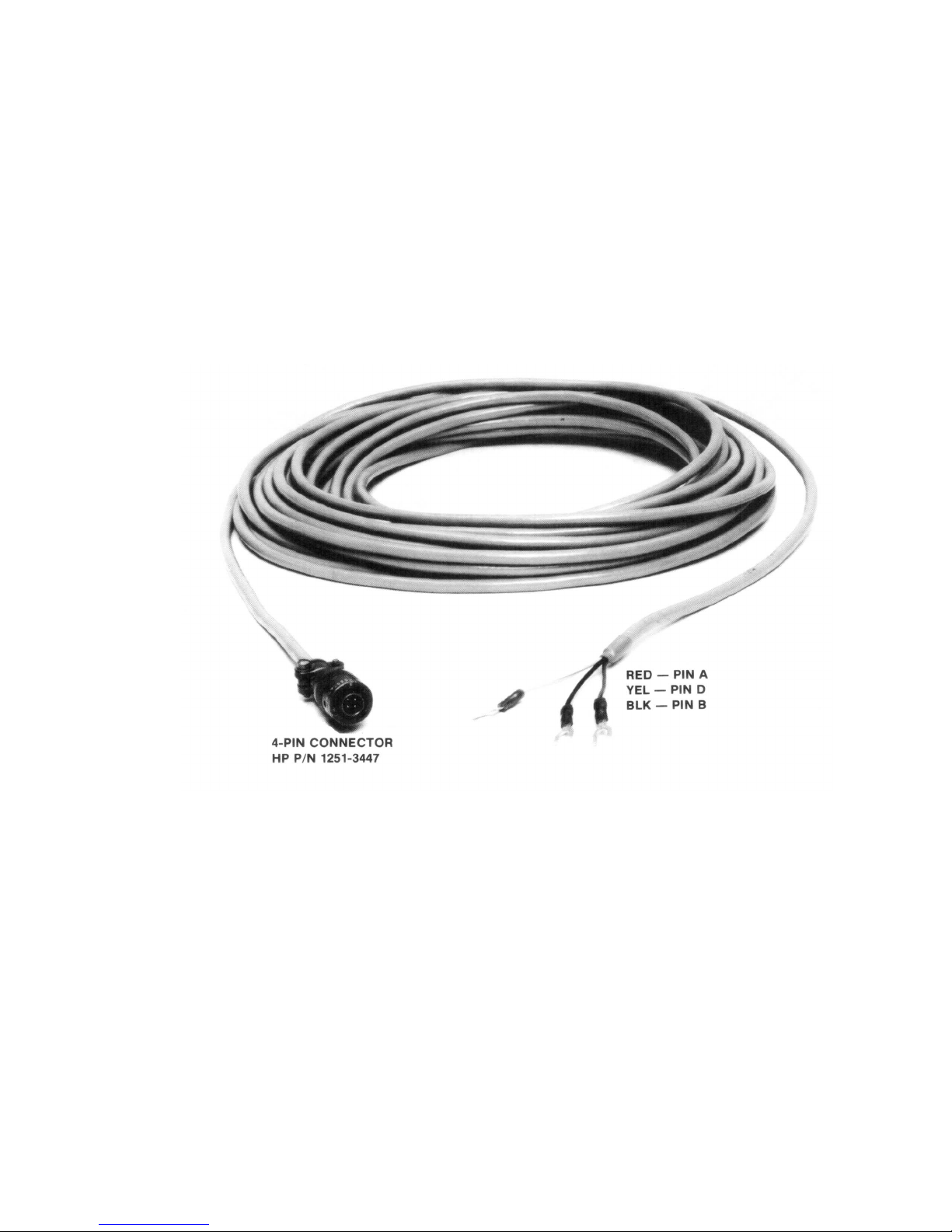
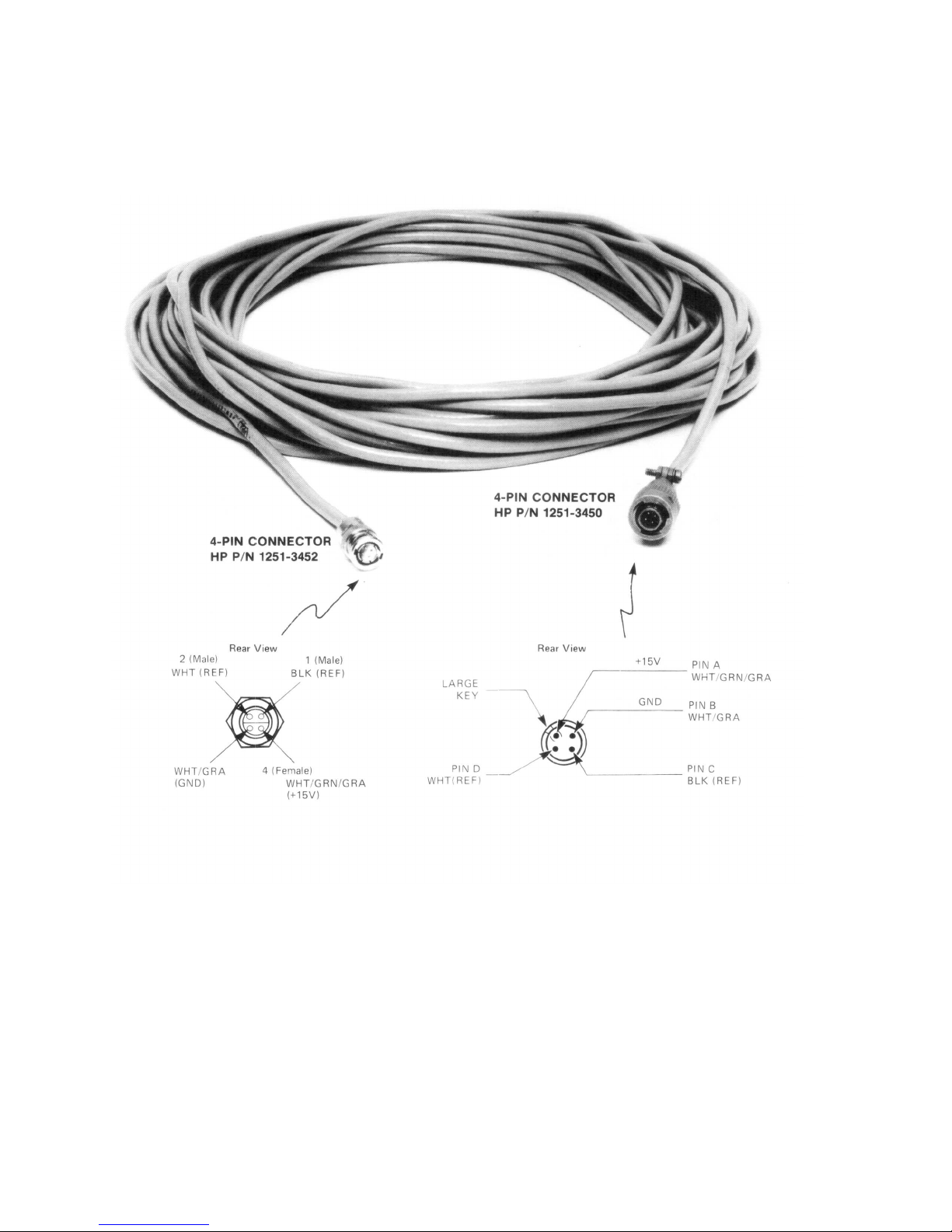
1-19. The HP 10778B and HP 10779B cables may be ordered from Hewlett-Packard. Figures 2-1 and
2-2 show photos of the cables, identify the connector markings, and give the pin numbers and
corresponding wire color codes.
*IEC, International Electrotechnical Commission
**CFR, Code of Federal Regulations (U.S.A.)
1-4
Page 17

HP5501B
Installation
1-20. Specifications
1-21. Table 1-1 lists the specifications and performance characteristics for the HP5501B Laser Head.
Table 1-1. HP5501B Laser Head Specifications and Performance Characteristics
Description: The HP5501B Laser Head contains an automatically tuned
Helium-Neon laser, circuits to control the laser, and a reference
optical receiver. The laser generates a coherent, collimated, two
frequency beam of light. This is a Class II Laser Product
conforming to U.S. National Center for Devices and Radiological
Health Regulations 21 CFR 1040.10 and 1040.11.
Environmental Conditions:
Temperature (Operating): 0 to 40°C (32 to 104°F)
Temperature (Non Operating): Can be stored or shipped in environments within the range of -
40 to +75°C.
NOTE
This unit should also be protected from temperature extremes that could
cause condensation within the instrument.
Relative Humidity (Operating): 0 to 95% Non-condensing
Vacuum Wavelength (Nominal): 632.991372 nanometers
Vacuum Wavelength Accuracy: 1 X 10⁻⁷
Vacuum Wavelength Stability: 2 X 10⁻⁸, typical
Beam Diameter: 6 mm typical
Maximum Beam Power Output: 1 milliwatt
Minimum Beam Power Output: 120 microwatts
Warm-Up Time: less than 10 minutes
Power Requirements: The HP5501B requires the following power inputs:
+15 Volts ±0.3 Volts at 0.8 Amperes maximum
-15 Volts ±0.3 Volts at 0.7 Amperes maximum
NOTE
Internal laser head 1.5 amp fuses permit power distribution to other laser
equipment.
Safety Features: Front shutter to block Laser Beam.
Outputs:
Reference signal: Differential square wave at approximately 1.8 MHz. Levels
Enclosure: NEMA Type 12
Dimensions: 32.5 X 13.2 X 12.7 cm
Weight:: 3.4 Kg (7.5 Ibs)
A safety switch disables high voltage when cover is removed.
compatible with all Laser Transducer System inputs.
1-5
Page 18

HP5501B
Installation
1-22. Recommended Test Equipment
1-23. The equipment required to maintain the HP5501B Laser Head is listed in Table 1-2. Other
equipment may be substituted if it meets or exceeds the critical specifications listed in the table.
Table 1-2. Recommended Test Equipment
RECOMMENDED
EQUIPMENT
INSTRUMENT USE*
CRITICAL SPECIFICATIONS
(Equipment Having
Equivalent Characteristics
May Be Substituted)
Signature
Multimeter
Oscilloscope T 100 MHz Bandwidth HP 1740A (if available)
Laser Power
Meter
Clip-on
Milliammeter
Logic Pulser T TTL level HP 546A
Current Tracer T Sensitivity: 1 ma to 1 amp HP 547A
Logic Clip T TTL Compatible 16-pin IC. mounting HP 548A
Logic Probe T
Digital Voltmeter T
*P = Performance Test; C = Calibration; A = Adjustments; T = Troubleshooting; S = Shortened
1-24. Warranty
T Detect TTL level signals HP 5005A/B
Range: 1 microwatt to 1 milliwatt
T
Accuracy: ±10%
United Detector Technology
Model 351L
T,A 10 ma range accuracy ±0.1 ma HP 428B
TTL/CMOS Capability with Pulse
HP 545A
DC Volts: Floating Inputs
Input Resistance: >10 MΩ
Range: 1, 10, 20 Volts DC
HP 3435A
Accuracy: 0.1%
Performance Test
1-25. The warranty statement for the instrument including the laser tube is located on the inside cover
of this manual.
1-6
Page 19

HP5501B
Installation
2 INSTALLATION
2-1. Introduction
2-2. This section provides installation instructions for the HP5501B Laser Head including unpacking,
inspection and reshipment, installation, operating environment, and storage. Installation includes
information on grounding considerations, power supply requirements, power dissipation, fusing,
dimensions, and mounting and fixturing.
2-3. Unpacking, Inspection, and Reshipment
2-4. The following paragraphs contain information for unpacking and inspection, warranty claims,
laser tube shipment, tagging for service, and packaging for reshipment.
TO AVOID HAZARDOUS ELECTRIC SHOCK, DO NOT PERFORM ELECTRICAL TESTS WHEN THERE ARE SIGNS OF SHIPPING DAMAGE TO ANY
PORTION OF THE OUTER ENCLOSURE (COVERS, PANELS, CONNECTORS,
LEOS, ETC.).
2-5. Unpacking and Inspection
2-6. Inspect the shipping container for damage. If the shipping container or cushioning material is
damaged, it should be kept until the contents of the shipment have been checked for
completeness and the instrument has been checked mechanically and electrically. Procedures
for checking electrical performance are given in
is mechanical damage or defect, or if the instrument or some component fails the performance
tests, notify the nearest Hewlett-Packard office. If the shipping container is damaged, or the
cushioning material shows signs of stress, notify the carrier as well as the Hewlett-Packard office.
Keep the shipping materials for the carrier's inspection. The HP office will arrange for repair or
replacement at HP's option without waiting for a claim settlement.
Section 4. If the contents are incomplete, if there
2-7. Warranty Claims
2-8. Contact the nearest HP Sales and Support Office (see list at the end of this manual) for
information relative to warranty claims.
2-9. Laser Tube Shipment
NOTE
The laser tube assembly MUST be shipped in an approved HP container.
2-10. The laser tube assembly (HP Part Number 05501-60102) should only be shipped in an HP
container designed for that purpose. In addition, the container must indicate that the laser tube
contains magnetic material. If it is necessary to ship a laser tube, contact your nearest HP Sales
and Support Office for an approved container.
2-1
Page 20

HP5501B
Installation
2-11. Tagging for Service
2-12. If the instrument is being returned to Hewlett-Packard for service, please complete one of the
blue repair tags (HP Part Number 9320-3896) located at the end of this manual and attaches it to
the instrument.
2-13. Packaging for Reshipment
1. Original Packaging
a. The same containers and materials used in factory packaging can be obtained through
Hewlett-Packard Sales and Support Offices listed at the rear of this manual.
b. In any correspondence refer to the equipment by model number.
2. Other Packaging Methods
a. If it becomes necessary to reship equipment, good commercial packing should be used.
b. Contract packaging companies can provide dependable custom packaging on short
notice. The following general instructions should be followed when repackaging with
commercially available materials.
c. If shipping to a Hewlett-Packard Support Office or Center, attach a blue tag indicating
the type of service required, return address, and model number.
d. Wrap the equipment in heavy paper or plastic.
e. Use a strong shipping container. A double-wall carton made of 350 pound test material
is adequate.
f. Use enough shock-absorbing material (three to four inch layer) around all sides of the
equipment to provide a firm cushion and prevent movement inside the container.
g. Seal the shipping container securely.
h. Mark the shipping container FRAGILE to assure careful handling.
2-14. Installation
2-15. The following paragraphs provide installation information for the HP5501B Laser Head including
system cabling, grounding considerations, power supply requirements, power dissipation, fusing,
and mounting and fixturing.
2-16. System Cabling
2-17. The HP5501B Laser Head is designed for use with the HP5501A Laser Transducer System and
is a direct replacement for the HP5501A Laser Head. The HP10778B Power and HP10779B
Reference cables (Figures 2-1 and 2-2 respectively), are available for connecting the laser head
to the laser transducer system.
2-18. The HP10778B and HP10779B cables are both 10 Meters (32.8 ft) in length.
2-2
Page 21
HP5501B
Installation
10778B LENGTH 10 METRES (32.8 FT)
Figure 2-1. HP 10778B Power Cable
2-3
Page 22
HP5501B
Installation
Figure 2-2. HP 10779B Reference Cable
2-4
10779B LENGTH 10 METRES (32.8 FT)
Page 23
HP5501B
Installation
2-19. Power and Signal Connections
2-20. The laser head rear panel contains two multi-pin connectors used for connecting HP5501B
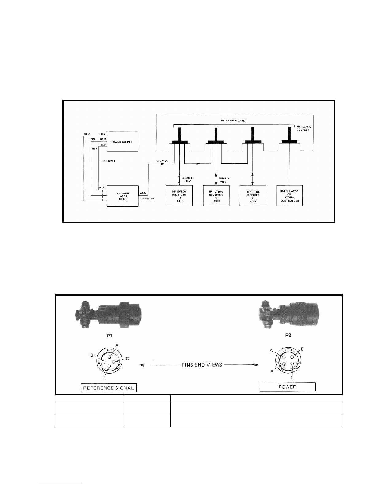
power and signal lines to other laser transducer system components. (Refer to Figure 2-3 for an
interconnection diagram of a typical system.) Table 2-2 lists all power and signal lines that are
available at the rear-panel connectors. The laser transducer system manual gives additional
system wiring information.
Figure 2-3. Typical Transducer System Interconnections
2-21. Cable Fabrication
2-22. Power and signal interconnecting cables of suitable length may be fabricated using the two
plugs included with the laser head. Figures 2-4 and 2-5 illustrate the physical details of the two
plugs supplied and give part numbers for both the plugs and the recommended cables. Refer to
Table 2-1 for rear-panel connector pin numbers of all available power and signal lines.
PLUG CABLE DESCRIPTION
REFERENCE SIGNAL
HP Part No. 1251-3450
POWER
HP Part No. 1251-3447
HP 10779B or
equivalent
HP 10778B or
equivalent
Dual coax; two #22 power wires.
Everything enclosed by a second insulated shield.
Three # 20 wires
Figure 2-4. Interconnecting Plug Details
2-5
Page 24
HP5501B
Installation
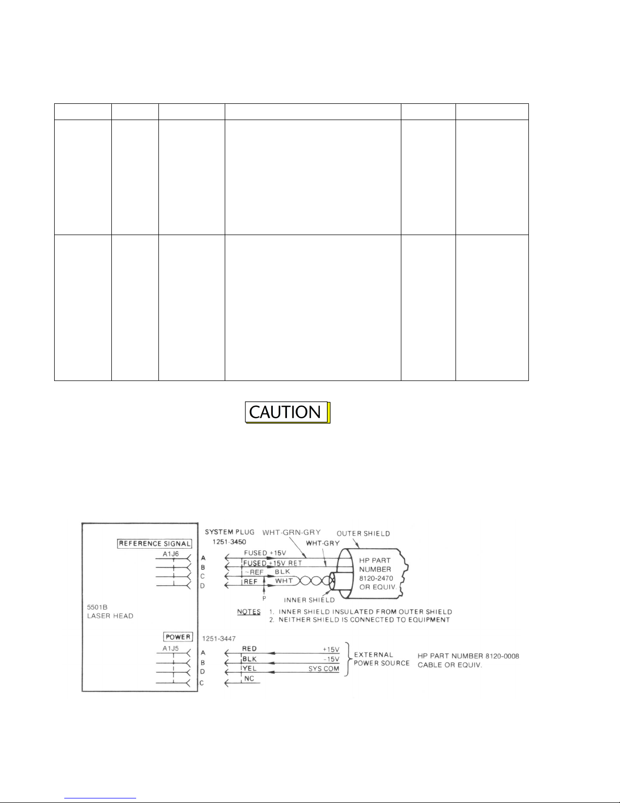
Table 2-1. Laser Head System Signal Chart
Input Output Signal Name Function Source Destination
A1J6-A Fused +15V Accessory +15V Operating Power
A1J6-B
A1J6-C REF
Fused +15V
RET
Accessory +15V Return
System REFerence signal, equal to
the difference in frequency between
A1J6-D -REF
laser beam components F1 and F2.
A1J5-A +15V External +15V Power Input
A1J5-B -15V External -15V Power Input
A1J5-C +5V +5V power test point
A1J5-D GND Power Ground
REF AND -REF OUTPUTS ARE CAPABLE OF DRIVING ONLY ONE UNIT
Ext. Pwr.
Sup.
Ext. Pwr.
Sup..
Ext. Pwr.
Sup
Accessory
Equipment
Accessory
Equipment
Accessory
Equipment
Accessory
Equipment
(test use only)
NOTE
THE RUBBER COLLAR WHICH GOES OVER THE CABLES IS A VERY
TIGHT FIT. USE SILICON GREASE TO FACILITATE INSTAILATION ON
CABLE.
Figure 2-5. HP 5501B Laser Head Interconnect Wire Fabrication
2-6
Page 25

HP5501B
Installation
Observe the current and grounding requirements described below.
2-23. Grounding Considerations
2-24. In order to avoid ground loops, the laser head base should be the only connection to earth
ground. To accomplish this, the outputs of the ±15 Volt power supplies used to power the laser
head should be floating. The +5 Volt power supply output required for either the HP10740A
based electronics or HP10781A Pulse Converters, should also be floating. Alternatively, any
other single point earth ground connection can be used to satisfy grounding requirements.
2-25. Power Supply Requirements
2-26. Table 2-2 lists the supply voltages, currents, and tolerances required by the HP5501B Laser
Head. Note that other components of the system also use ±15 Volts. Add these to the laser
head current requirements to obtain the overall system requirements.
Table 2-2. HP 5501B Power Supply Requirements
Supply Voltage Tolerance Current Requirement
+15 Volts ±0.3 Volts 0.8 Amperes
3.5 Amperes peak surge for
-15 Volts ±0.3 Volts 0.7 Amperes
Other Power Supply Requirements
Line Regulation 0.01%
Load Regulation 0.01%
Ripple + Noise 60 millivolts peak-to-peak
Isolated Output
Over Voltage Protection
(Recommended)
Under Voltage Protection
(current limited)
(Recommended)
approximately 2 milliseconds
at power-up
2-27. Power Dissipation
2-28. The HP5501B dissipates approximately 21 watts during operation.
2-29. Fusing
2-30. The HP5501B has two internal 1.5 Ampere fuses to protect the ±15V lines. Both fuses are
located on the A1 Connector Board and are accessible by removing the left and right covers of
the laser head.
2-7
Page 26
2-31. Dimensions
2-32. Figure 2-6 shows the HP5501B Laser Head dimensions.
DIMENSIONS IN MILLIMETERS
HP5501B
Installation
Figure 2-6. Mounting Details and Physical Characteristics
2-8
Page 27

HP5501B
Installation
2-33. Mounting and Fixturing
2-34. Heat Flow Considerations. The laser tuning technique of the HP5501B requires efficient heat
exchange with the ambient. Heat flow is primarily through the base of the laser head assembly to
the surrounding environment. An external heat sink is not required but free air circulation around
the laser head will ensure good performance.
2-35. In cases where vertical mounting of the HP5501B is desired, care should be taken to minimize
laser beam disturbances due to air turbulence caused by the HP5501B heat exchange. It is most
important to prevent differential effects which can occur due to turbulence in the beam path
between a polarizing beam splitter and a retroreflector or plane mirror. Differential turbulence
causes fluctuations in the optical path length difference that is being measured. Both differential
and common mode turbulence can cause fluctuations in alignment by bending the light beam.
Common mode turbulence is turbulence that is present in the beam path between the HP5501B
and a polarizing beam splitter. In either case some amount of noise can be present in the
interferometer measurement due to turbulence.
2-36. If interferometer components (optics) are mounted very close to the HP5501B such that the
operating temperature of the optics are affected, it is recommended that alignment and
operation of the interferometer be performed after the HP5501B has been running for a sufficient
period of time to allow thermal equilibrium to be established. In well ventilated installations, one
hour of running time should be sufficient. When enclosures are used and the ambient
temperature is changed by several degrees (centigrade) by the HP5501B, thermal equilibrium is
not established as quickly and the laser should be run for a longer period of time.
2-37. Mounting. Mount the laser head by means of the three slotted tabs that extend outward from the
bottom edges of the unit (refer to Figure 2-1 for exact locations and dimensions). The mounting
tabs may be secured to the work surface in any fashion that will not transmit stresses to the main
enclosure and, consequently, to the laser tube or printed-circuit assemblies. If necessary, the
tabs can be removed and the unit mounted on a flat surface with 4 mm machine screws; use the
same tapped holes that are used to secure the tabs, ensuring that the mounting method does
not stress the base casting and that the screws do not penetrate the base casting more than 7
mm.
2-38. Beam Alignment. Rotate the turret at the front of the laser head so that the beam exits through
the large aperture. DO NOT STARE DIRECTLY INTO THE BEAM APERTURE. Presence of the
red laser beam can be verified by placing a piece of paper in the beam path and observing the
beam reflection on the paper. The components of the laser transducer system must now be
aligned so that the laser beam strikes the photodetector of the receiver (HP10780A). Refer to the
HP10780A Receiver documentation and the Laser Transducer System Manual for further
alignment information.
2-39. Pointing Stability. The angle at which the laser beam exits the HP5501B can change from turn-
on through the time when the HP5501B and its surroundings reach thermal equilibrium.
2-40. The HP5501B should not be exposed to ambient temperature changes greater than ±5
Centigrade during operation to keep pointing stability variations to a minimum during
interferometer measurements.
2-9
Page 28
HP5501B
Operation
3 OPERATION
3-1. Introduction
3-2. This section provides operating information for the HP5501B Laser Head. Included are operation
features of the instrument's front and rear panel controls and connectors. Also provided is
supplemental operating information for HP5501A Laser Transducer Systems equipped with
HP5501B Laser Heads.
3-3. Installation instructions for the HP5501B Laser Head are given in
Section 2 of this manual.
3-4. Power Application
3-5. The laser head installed is activated when +15 Vdc and -15 Vdc are applied to the unit. ±15
Volts is applied by connecting the power cable (HP10778B or fabricated equivalent) to the rear
panel POWER connector (A1J5). Ensure that the power source is adjusted to conform to the
following requirements before connecting it to the HP5501B:
Measured Voltage +15V ± 0.3 Vdc -15V ± 0.3 Vdc
NOTE
REPETITIVE POWER-UP CYCLING SHOULD BE AVOIDED. THIS WILL
REDUCE THE EXPECTED LIFE OF THE HIGH VOLTAGE
COMPONENTS.
3-6. HP5501B Laser Head Front Panel Controls
3-7. Figure 3-1 identifies and describes each of the operating controls, connectors, and indicators.
Refer to Table 2-1 for information regarding the specific power and signal/lines at each of the
connectors.
Figure 3-1. HP5501B Front Panel Controls
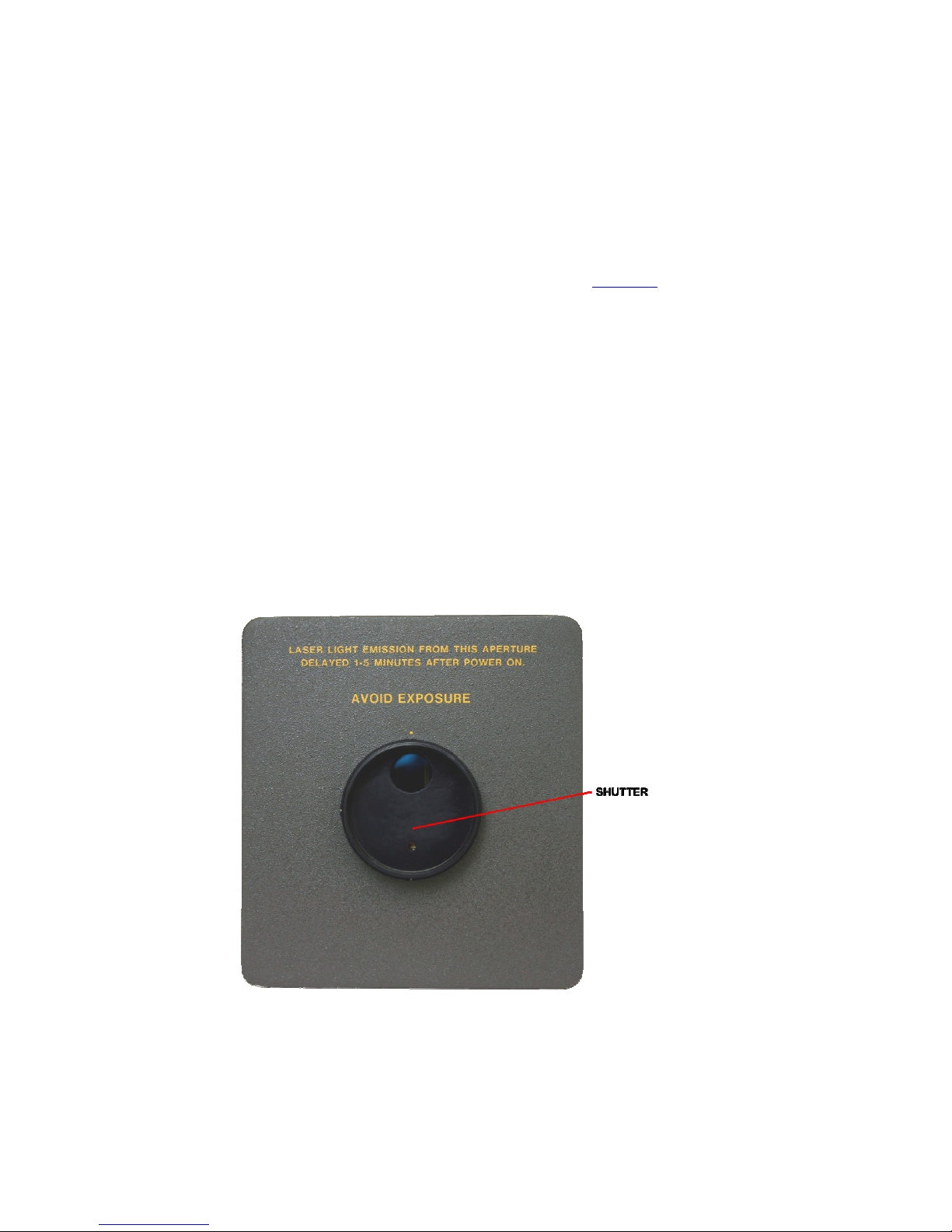
1. Shutter: The shutter, also known as the aperture ring, allows for three aperture
settings: open, reduced, and closed. The open aperture position is used during
normal operation and the reduced aperture is used during alignment of
measurement axes.
3-10
Page 29
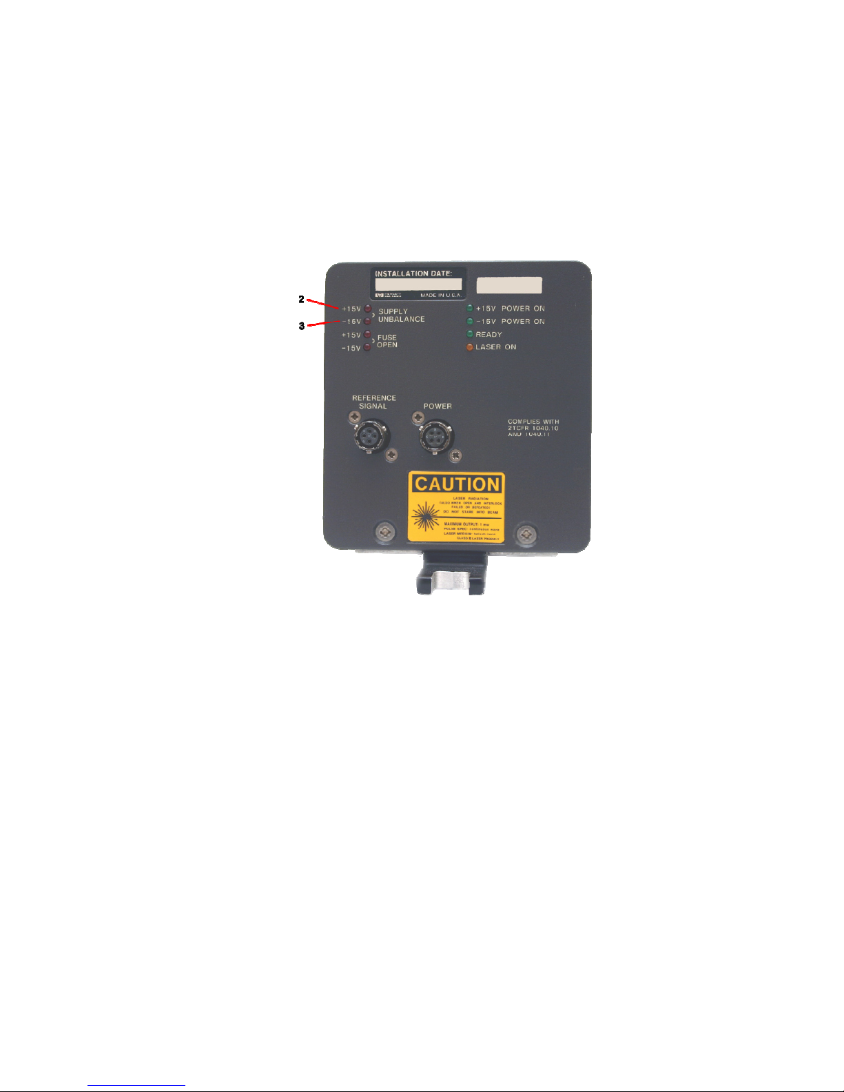
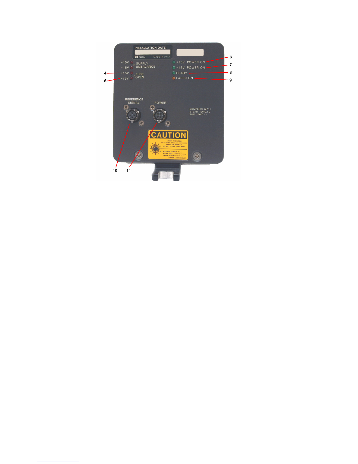
3-8. HP5501B LASER HEAD REAR PANEL INDICATORS AND CONNECTORS
NOTE
A TILDE ("~") PRECEDING A SIGNAL NAME INDICATES NEGATIVETRUE LOGIC LEVELS.
3-9. Following are descriptions of the HP5501B rear panel features shown in Figure 3-2.
HP5501B
Operation
2. +15V SUPPLY
UNBALANCE
3. -15V SUPPLY
UNBALANCE
Figure 3-2. HP5501B Rear Panel Connectors and Indicators
RED
LED
RED
LED
LED lights if the ±15V input voltages are unbalanced
in the positive direction by one Volt or more. For
example:
When the positive supply measures +16 Volts (or
more positive) and the negative supply remains at 15 Volts.
When the positive supply measures +15 Volts and
the negative supply is -14 Volts (or less negative).
LED lights if the ±15V input voltages are unbalanced
in the negative direction by one Volt or more. For
example:
When the negative supply measures -16 Volts (or
more negative) and the positive supply remains at
+15 Volts.
When the negative supply measures -15 Volts and
the positive supply is +14 Volts (or less positive).
Both ±15V SUPPLY UNBALANCE LED’s light if the
TEST-NORM switch (A1S2) is in NORM position with
cover off or in TEST with cover on.
3-11
Page 30
HP5501B
Operation
4. +15V FUSE OPEN RED LED LED lights if +15 Vdc fuse opens.
5. -15V FUSE OPEN RED LED LED lights if -15 Vdc fuse opens.
6. +15V POWER ON GREEN LED LED lights when +15 Vdc power is applied
to the HP5501B.
7. -15V POWER ON GREEN LED LED lights when -15 Vdc power is applied to
the HP5501B.
8. READY GREEN LED LED remains off while heating rod to normal
operating temperature. At this point the
READY LED begins to flash and continues to
do so until the laser head reaches operating
temperature. When the laser head is ready
for use, the READY LED stays on steady
(i.e., Laser has achieved lock and is now
generating a stable reference signal).
9. LASER ON AMBER LED LED lights to indicate that the high voltage
power supply (HVPS) is on and that laser
light is being emitted.
10. POWER CONNECTOR
(A1J5)
Provides connection point for external power
supply input (i.e., 10778B Power Cable
connector).
11. REFERENCE CONNECTOR
(A1J6)
Allows the reference signals (REF and -REF),
and +15 power to be connected to other
system components (i.e., 10779B Reference
Cable connector).
Figure 3-2. HP5501B Rear Panel Connectors and Indicators (Continued)
3-12
Page 31

HP5501B
Operation
3-10. OPERATING MODES
3-11. When power is applied to the HP5501B, an internal state machine resets the laser head to a
warmup mode. This mode is used to establish the initial operating temperature of a glass rod
that controls the laser cavity length. When this temperature is reached, the state machine
switches to an optical tuning mode. Upon successfully switching from warmup to optical mode,
the laser head enables the REFerence signal and lights a READY LED indicator on the rear panel
to indicate that the laser head is ready for use. The following table will give the proper operating
sequence for the HP5501B rear panel Led's from initial power-up (warmup mode) to when the
laser is ready to use (optical mode).
Table 3-1. Proper 55018 Rear Panel LED Power-up Sequence
OPERATING MODES*
WARMUP OPTICAL
LED’s
+15V SUPPLY
UNBALANCE
(Red LED)
-15V SUPPLY
UNBALANCE
(Red LED)
+15V
FUSE OPEN
(Red LED)
-15V
FUSE OPEN
(Red LED)
+15V
POWER ON
(Green LED)
-15V
POWER ON
(Green LED)
READY
(Green LED)
LASER ON
(Amber LED)
↑
15V Applied
to Laser
Head. Heater
Full On
*Time intervals reflect that laser tube was cold at turn-on; shorter times can be expected if tube is warm
at turn-on.
**Refer to paragraph 8-100 for further explanation of laser operating modes.
PREHEAT HEATER
LOCKING LOCKED
QUALIFIED
←3-6 Min**→
← 100 sec → ← 50 sec → Continuous use
OFF OFF OFF OFF
OFF OFF OFF OFF
OFF OFF OFF OFF
OFF OFF OFF OFF
ON ON ON ON
ON ON ON ON
OFF Flashing 2Hz Flashing
ON
2Hz
OFF OFF ON ON
↑
Glass rod
reaches
temperature
(begin 100
second
↑
HVPS Turns
on
Laser Beam
on
↑
Reference
signal
present
Laser now
ready for use
stabilization
period
3-13
Page 32

3-12. Warmup Time Operating Notes
• Allow a full 10 minute warmup period for the HP5501B.
• Warmup completion is indicated by the READY LED on the HP5501B rear panel.
• If warmup is not complete after 10 minutes, a failure may be indicated.
• If the READY indication at the laser head is not convenient to use because of the mounting
scheme, try the alternate monitoring suggestions that follow.
3-13. HP 10740A Coupler Based Systems - Manual Monitoring
• The REFerence and MEASurement signals terminate at either the HP10760A Counter Card
or the HP10764A/B/C Fast Pulse Converter Card.
• Each of these cards includes an LED to monitor the presence of the REFerence and
MEASurement signals.
• The REFERENCE LED will be extinguished until the HP5501B is ready for use.
HOWEVER, FOR SYSTEMS WITH MULTIPLE HP 10760A CARDS
• Every ODD HP10760A that uses the replicated REF and -REF will have their REFERENCE
LED lit during the laser head warmup period. (This is due to inversion in the replication
circuitry.) Note that this does not apply to multiple HP10764A/B/C card installations.
• The MEASUREMENT LED will momentarily light several times during the laser head warmup
period provided that the HP10780A Receiver is aligned properly with the beam. (This occurs
because the laser periodically produces functional optical frequencies during warmup.)
NOTE
The above monitoring scheme assumes no reversal of the REF and -REF lines in the cabling.
3-14. Systems with HP10745A or HP10746A Cards - Automatic Monitoring
HP5501B
Operation
3-15. Systems with these cards can use the system computer and software to monitor the laser head
warmup. Before describing the software, it will be helpful to examine some background
information on the HP10740A Coupler, HP10745A HP-IB Interface, and HP10746A Binary
Interface.
3-16. HP10740A Coupler - Error Signal Information
• Four error signal lines are provided on the HP 10740A Backplane:
- REFERENCE ERROR BIT
- MEASUREMENT ERROR BIT
- V.O.L. ERROR BIT
- OVFL BIT
3-14
Page 33

HP5501B
Operation
3-17. HP10746A Error Signal Processing
• If any of the HP10740A backplane error bits are true, the four most significant bits of the
most significant word in a data transfer from the HP10746A to the host computer will be all
ones. These four bits are normally the decimal point bits.
• Errors are not the only condition that can set these bits to all ones. When the difference
output of an addressed HP10762A is within tolerance, these bits will also be set.
• After detecting all ones, the host computer must check the next four MSB's to differentiate
between an error condition and the within tolerance condition.
• If the tolerance condition is true, these next four bits will also be all ones. Otherwise, each of
these bits corresponds to one of the backplane error bits.
3-18. HP 10745A Background Information
• When a backplane error bit is true, the HP10745A asserts SRQ. The STATUS BYTE of the
HP10745A can be read to determine the source of SRQ. I n the STATUS BYTE, bit 0
corresponds to the REFERENCE ERROR-BIT.
3-19. Program Modifications
3-20. To monitor warmup time, the following program modifications can be added to the example
programs contained in Tables 4-12 and 4-13 of the HP5501A Laser Transducer Operating and
Service Manual, HP Part Number 05501-90028. If desired, some form of time-out algorithm can
be added to check if the HP5501B warms up within 10 minutes.
3-21. Table 3-1 shows the program steps used to modify Table 4-12 in the HP5501A System Manual.
The program uses the HP10760A x-axis card to monitor the laser warmup.
3-22. Table 3-2 shows the program steps used to modify Table 4-13 in the System Manual. The
program is for a two axis system with the HP10746A in 16-bit mode and using positive-true logic.
The program uses the x-axis card to monitor the laser warmup.
3-23. Tables 3-3, 3-4, and 3-5 are complete listings of the modified versions of Tables 4-12 and 4-13
found in the HP5501A System Manual.
3-15
Page 34

HP5501B
Operation
Table 3-1. Program Modifications for Table 4-12 in the HP5501A System Manual
0: gsb "warmup"
38: "warmup":clr 7; rem 7
39: wrt 709,"0O0X"
40: wrt 709,"1X2X3O"
41: if rds(7)<128; ret
42: rds(709)→B
43: if B<64;gto "bus error"
44: B-112→B
45: if B>=8;B-8→B
46: if 8>=4;B-4→B
47: if B>=2;B-2→B
48: if B=1;dsp "LASER NOT READY"
49: if B=1;gto -11
50: gsb "check"
51: ret
52: "bus error":
53: prt "SRQ ASSERTED BUT 10745A
STATUS BYTE,BIT6 CLEAR”
54: stp
Branch to subroutine to monitor laser
status
Send Device Clear: Send Remote Enable
Send 10740A Backplane reset preset xaxis counter and select normal
resolution
Transfer x-axis counter (10760A),
contents including error bits to 10745A
If SRQ false ~REFERENCE ERROR BIT must
be false laser ready
Read 10745A STATUS BYTE to verify that
it is asserting SRQ
If 10745A not asserting SRQ; alert
operator.
Isolate ~REFERENCE ERROR BIT
If true; 5517A not READY
Try again
Otherwise, use subroutine “check” to
identify remaining error
Return to step one if only ~OVF ERROR
true
Alert operator that another device
asserted SRQ
3-16
55: gto 0
56: end
Return to step 0 if CONTINUE pressed
Page 35

HP5501B
Operation
Table 3-2. Program Modifications for Table 4-13 in the HP5501A System Manual
0: gsb "warmup"
66: "warmup":wtb 2,0,0,0
67: wtb 2,1,130, 3
68: rdb(2) →B;if B<0;65536+B→B
69: if B<61440; ret
70: int(B/256)240→B;15-B→B
71: if B>=8;B8→B
72: if B>=4;B4→B
73: if B>=2;dsp "LASER NOT READY"
74: if B>=2;sto -8
75: wtb 2,1,130, 3
76: rdb(2) →B;if B<0;65536+B→B
77: gsb "er"
78: ret
79: end
Branch to warmup subroutine monitor laser status
System reset 10746A in 16 bit mode
1 = simultaneous sample
130 = transfer X Comparator Counter contents to
10746A
3 = prepare for output to host computer
Read first word
If 4 MSB's are clear, 5517A is READY
Otherwise isolate ~REFERENCE ERROR BIT
If ~REFERENCE ERROR BIT true, try again
Abort transfer and setup new transfer in order to
read first word again.
Use subroutine "er" to identify remaining error
Return to program step 1 only if ~OVL ERROR BIT is
true
3-17
Page 36

Table 3-3. Modified HP10745A HP-IB Interface Program
0: gsb "warmup"
1: wrt 709,"0O6X"
2: wrt 709,"2V3O"
3: red 709,C
4: 0→E
5: "loop": E+1→E; if E=10;gto -3
6: wrt709,"1O2X3O"
7: red 709,X
8: if rds(7)<128;gto +2
9: 0→A; gsb "status"
10: (X-16)*6.23023e-6*C→X
11: fmt 1,f12.6
12: dsp X
13: gto "loop"
14: "status":rds(709)→B
15: if B>=64;gsb "check"
16: wrt 709,"0P"
17: ret
18: "check": B-112→B
19: if B>=8;gsb "ovf"
20: if B>=4; prt "VOL OUT OF RANGE";B-4→B;0→D
21: if B>=2; prt "MEAS ERROR";B-2→B;0→D
22: if B=1; prt "REF ERROR";0→D
23: if D=2; ret
24: if A=0; prt "X-AXIS ERROR"
25: if A=1; prt "Y-AXIS ERROR"
26: dsp "GO TO GAGE"; stp
27: gto 0
28: "ovf":B-8→B; 1→D
29: if A=0;X-2^28/10→X
30: if A=1;Y-2^28→Y
31: ret
32: "warmup": clr 7; rem 7
33: wrt 709,"0O0X"
34: wrt 709,"1X2X30"
35: if rds(7)<128;ret
36: rds(709)→B
37: if B<64;gto "bus error"
38: B-112→B
39: if B>=8;B-8→B
40: if B>=4;B-4→B
41: if B>=2;B-2→B
42: if B=1;dsp "LASER NOT READY"
43: if B=1;gto -11
44: gsb "check"
45: ret
46: "bus error":
47: prt "SRQ ASSERTED BUT 10745A STATUS BYTE, BIT6 CLEAR"
48: stp
49: gto 0
50: end
HP5501B
Operation
3-18
Page 37

Table 3-4 Modified HP10746A Binary Interface Program
0: gsb "warmup"
1: wtb 2,0,0,0,98,3
2: gsb "in"
3: B→C
4: ent "X TOLERANCE IN MICRONS?",r1
5: ent "Y TOLERANCE IN MICRONS?",r2
6: "newdest":0→X;ent "X DESTINATION IN MM?",X
7: 0→Y;ent "Y DESTINATION IN MM?",Y
8: "comp":wtb 2,98,3
9: gsb "in"
10: B→C
11: X→A;gsb "cnv"
12: A→X
13: Y→Ajgsb "cnv"
14: A→Y
15: int(r1/1.58248e-1)*2^228+X→A
16: gsb "out"
17: wtb 2,131
18: int(r2/1.528248e-1)*2^228+Y→A
19: gsb "out"
20: wtb 2,147
21: "newsample":wtb 2,1,130,3
22: 0→F
23: gsb "in"
24: B→r3
25: wtb 2→146,3
26: I→F
27: gsb "in"
28: B→r4
29: fmt 1,2fI0.0,fI0.7
30: wrt .1,r3-160,r4-160,C
31: if abs(X-r3) <= r1/1(.158*C) and abs(Y-r4) <= r2/1(.158*C); gto "newdest"
32: gto "newsample"
33: "in":rdb(2)→B if B(0;65536+B→B
34: if B>=61440;gto "er"
35: rdb(2)→G;if G(0;65536+G→G
36: int(B/14096) →D
37: B-4096*D→B
38: (65536*B+G)*tn^(2-D)→B;ret
39: "cnv":A/1(1.58248e-4*C)+160→A;ret
40: "out":wtb 2,4
41: int(A/165536)→B;if B>32767;B-65536→B
42: wtb 2,B
43: A-65536*intCR/165536)→B;if B>32767;B-65536→B
44: wtb 2,B
45: ret
46: "er":int(B/1256)-240→B; 15-B→B
47: if B>=8;prt "vol error";B-8→B;0→D
48: if B>=4;B-4)B;1→D
49: if B>=2;prt "ref error";0→D
50: if B=I;prt "meas error";0→D
51: if D:0;gto "prterr"
52: rdb(2) →B
53: wtb 2,240,3
54: rdb(2)→B; if B<0;65536+B→B
55: rdb(2)→G;if G<0;65536+G→G
56: int(B/4096)→D
57: B-4096*D→B
58: (65536*B+G)*tn^(2-D)→B
59: if F=0 and B-160#0;B-2^28→B
60: if F=1 and B-160#0;B-2^28→B
61: ret
HP5501B
Operation
3-19
Page 38

62: "prterr": if F=0;prt "X-AXIS ERROR"
63: if F=1;prt "Y-AXIS ERROR"
64: dsp "GO TO GAGE";stp
65: gto 0
66: "warmup":wtb 2,0,0,0
67: wtb 2,1,130,3
68: rdb(2)→B;if B<0;65536+E→B
69: if B<61440;ret
70: int(B/256)-240→B;15-B→B
71: if B>=S;B-S→B
72: if B>=4;B-4→B
73: if B>=2;dsp "LASER NOT READY"
74: if B>=2;gto -S
75: wtb 2,1,130,3
76: rdb(2)→B; if B<0;65536+B→B
77: gsb "er"
78: ret
79: end
HP5501B
Operation
3-20
Page 39

HP5501B
Performance Tests
4 PERFORMANCE TESTS
4-1. Introduction
4-2. This section contains a performance test for the HP5501B Laser Head. A test record is
included to record test results for future comparison.
4-3. RECOMMENDED TEST EQUIPMENT
4-4. Test equipment requirements are included in the following procedure. Detailed critical
specifications for the required test equipment are contained in Table 1-2, Recommended
Test Equipment. Any equipment that satisfies the critical specifications given in the table
may be substituted for the recommended model(s).
4-5. TEST RECORD
4-6. Results of the performance test may be tabulated on the test record at the end of these
procedures.
4-7. HP5501B PERFORMANCE TEST
4-8. The HP5501B performance test consists of measuring the HP5501B input voltages and
laser power output.
4-9. Input Voltage Check
4-10. Check the HP5501B voltages in the following manner:
Disconnect the POWER cable.
Measure the voltages at the disconnected cable plug as outlined in Table 4-1.
Table 4-1. Input Voltage
Plug Pin Voltage
A1J5 (A) +15 ±0.3 Vdc
A1J5 (B) -15 ±0.3 Vdc
4-11. Laser Power Output Test
4-12. Test Equipment Required. The following test equipment is required to test the laser
output power.
Laser Power Meter, United Detector Technology (Model No. 351L)
4-1
Page 40

4-13. Procedure
a. Connect the HP5501B to the HP5501A system (or any suitable dual DC voltage
power supply such as the HP6255A) using HP10778B Power Cable as shown in
b. On the HP5501B, set the exit shutter of the turret assembly to its open aperture
position.
c. Turn the ±15 Volt power supply on and wait until the READY indicator is on, not
blinking. This should occur less than 10 minutes after power is applied.
d. Using the Laser Power Meter, align the power meter detector for maximum
reading.
Laser beam must fall totally within the active region of the power meter's detector.
e. If the laser power output is less than 120 microwatts, perform the laser tube
current adjustment procedure in
HP5501B
Performance Tests
Figure 4-1. HP5501B Power Connection
NOTE
Section 5.
4-2
Page 41

HP5501B
Adjustments
5 ADJUSTMENTS
5-1. Introduction
5-2. This section describes adjustments and checks required to return the HP5501B Laser Head to
peak operating capabilities when repairs have been made. Included in this section are the test
equipment required, equipment setups, and procedures to perform the adjustments.
5-3. Safety Considerations
5-4. The following warnings contain information that must be understood for your safety.
FROM 1.2 KILOVOLTS TO 12 KILOVOLTS DC IS PRESENT ON THE
ANODE OF THE LASER TUBE IN THE HP5501B. EXERCISE
EXTREME CAUTION WHEN WORKING INSIDE THE INSTRUMENT.
THE HIGH VOLTAGE COULD CAUSE SERIOUS PERSONAL INJURY
IF CONTACTED. THE FOLLOWING ADJUSTMENTS SHOULD BE
PERFORMED BY SERVICETRAINED PERSONNEL.
NOTE
The High Voltage Power Supply, A2, is disconnected automatically by
A1S1, when the HP5501B covers are removed. For Adjustments and
Servicing purposes, the High Voltage Supply can be re-enabled by
setting the TESTNORM switch, A1S2, to TEST after the HP5501B covers
are removed.
LASER RADIATION IS ACCESSIBLE WHEN THE HP5501B COVERS
ARE REMOVED AND THE TEST-NORM SWITCH, A1S2, IS IN THE
TEST POSITION.
5-5. Recommended test equipment
5-6. Test equipment required for each adjustment is included in the adjustment procedure. Detailed
critical specifications for the required test equipment are contained in Table 1-2. Any equipment
that satisfies the critical specifications given in the table may be substituted for the
recommended model(s).
5-7. Factory Selected Components
5-8. As of the publication date on the title page of this manual there are no factory selected
components.
5-1
Page 42

HP5501B
Adjustments
5-9. Adjustment Procedures
5-10. The following paragraphs contain the adjustment procedures for the HP5501B Laser Head. A
performance test is given in
Section 4.
5-11. Reference Temperature Adjustments
5-12. This adjustment sets the laser preheat temperature to 105°C (221°F). The adjustment must be
performed when the laser tube is at room temperature, 21 to 25°C (69.8 to 77.0°F).
5-13. Test Equipment Required. The reference temperature adjustment requires the following test
equipment: Digital Voltmeter, HP Model 3435A
5-14. Preliminary Procedure
5-15. This adjustment must be made with the laser tube at room temperature. If the laser High Voltage
Power Supply (A2) or heater has been on, allow at least two hours with ±15 Volts off before
performing this procedure. Regardless of whether power is on or off, observe the safety
precautions in paragraph 5-4 and proceed as follows:
Remove the HP5501B Laser Head covers by following the procedure outlined in paragraph 8-55.
a. Check that the TEST-NORM switch (A1S2) located on the A1 Connector Board is set to
NORM. See Figure 5-1.
Figure 5-1. A1 Connector Board, TEST-NORM Switch and Adjustment Locations
5-2
Page 43

b. On A3, change the HEATER jumper from NRM to OFF. See Figure 5-2.
c. Apply power to the Digital Voltmeter and set its controls to the 1 Volt DC range. Connect
the positive lead of the Digital Voltmeter to A3TP11 then connect the negative lead to
A3TP1. See Figure 5-2.
d. If HP5501B power has been disconnected for least 2 hours, reconnect ±15 Volts system
power supplies and continue with the adjustment procedure in Paragraph 5-16.
5-16. Procedure to adjust the reference temperature, proceed as follows:
a. Check that the Voltmeter reads between +0.22V and +0.31V. This voltage is V(A3TP11).
b. Record value of V(A3TP11) measured in step 5-16(a).
c. Calculate the heater adjust set point using the following equation:
d. Vset = 1.285 x V(A3TP11)
e. Connect Digital Voltmeter plus lead to A3TP15. Connect the minus lead to A3TP1. See
Figure 5-2.
f. Check that the voltage at A3TP15 equals Vset ± 1 millivolt as calculated in step b. If not,
adjust A3R16 SET TEMP (see Figure 5-2).
g. Note and record the SET TEMP voltage in the "ADJUSTMENT RECORD" table located at
the end of this section.
h. Disconnect ±15 Volts from HP5501B Laser Head.
i. On A3, change the HEATER jumper back to NRM (left-most position). Remove the test
equipment leads, and reinstall the laser head covers.
HP5501B
Adjustments
Figure 5-2. A3 Controller/Ref Board, Jumpers, Test Points, and Adjustment Locations
5-3
Page 44

HP5501B
Adjustments
5-17. Laser Tube Current Adjustment
NOTE
A TILDE (“~”) PRECEDING A SIGNAL NAME INDICATES NEGATIVETRUE LOGIC LEVELS.
5-18. This procedure adjusts the laser tube current to 3.5 milliamperes ± 0.1 milliampere.
Test Equipment Required. The laser current adjustment requires the following test equipment:
Clip-On DC Milliammeter, HP Model 428B
5-19. Procedure to adjust the laser tube current, observe the safety precautions in Paragraph 5-4 and
proceed as follows:
a. Turn the system power supplies OFF.
b. Remove the laser head covers by following the procedures outlined in paragraph 8-55.
c. On the A1 Connector Board, set TEST-NORM (A1S2) switch to TEST. See Figure 5-1.
d. Set indicated jumpers to the following positions:
1. JMP2 (~REF ON) .........................LO
2. JMP4 (HTR OK) ............................HI
3. JMP7 (HEATER) ...........................OFF
4. JMP8 (CLK FREQ) ........................HI
NOTE
Setting the A3 jumpers causes the laser to come on soon after power is
applied.
e. Set the milliammeter to the 10 milliampere range.
f. Clip the HP428B probe around the red (Anode) High Voltage Power Supply wire located
underneath the laser tube (See Figure 5-3). The arrow on the milliammeter probe should
point away from the supply. Keep the probe as far as possible from and perpendicular to
the magnet assemblies. It may be necessary to prop up the probe to achieve the
perpendicular orientation.
g. On the milliammeter, adjust for zero indication. If zero indication cannot be obtained,
degauss the probe as directed on the back of the milliammeter.
NOTE
After the zero setting has been made on the milliammeter, do not move
the probe, this will affect the zero setting.
5-4
Page 45

HP5501B
Adjustments
h. Apply power to the system power supplies.
NOTE
READY LED will flash rapidly for about 5 seconds. LASER LED
illuminates followed almost immediately by emission of laser light.
i. Adjust A1R12 (Figure 5-1) for 3.5 milliamperes ± 0.1 milliampere. If the current cannot
be adjusted to this value, see Laser High Voltage Troubleshooting in
Section 8. If the
laser power output (as measured in paragraph 4-9) is not greater than 120 microwatts
(at this current level), the laser assembly may require replacement.
j. Record the laser tube current in the "ADJUSTMENT RECORD" located at the end of this
section.
k. Turn off the system power supplies, disconnect the probe, set the TEST-NORM switch to
NORM, and reinstall the laser head covers.
l. Return all A3 jumpers, moved in step 5-20(d), back to NRM position (left-most position).
Figure 5-3. 55018 High Voltage Areas and Anode Lead
5-5
Page 46

Page 47

HP5501B
Replaceable Parts
6 REPLACEABLE PARTS
6-1. Introduction
6-2. This section contains information for ordering replacement parts. Part numbers for replacement
parts are provided in either illustrated parts breakdown or tabulated listings depending on the
type of part. Purchase Order and Direct Mail Order information are provided in Paragraphs 6-9
through 6-13.
6-3. Table 6-1 is a list of exchange assemblies and Table 6-2 gives abbreviations and reference
designators used in the parts lists and throughout the manual. Table 6-3 lists replaceable parts
that are mounted on pc board assemblies. Table 6-4 contains the names and addresses that
correspond to the manufacturer's code numbers given in Table 6-3. Figure 6-1 shows illustrated
parts breakdowns showing the chassis mounted parts and assemblies for the HP5501B.
6-4. Exchange Assemblies
6-5. Table 6-1 lists assemblies within the HP5501B Laser Head that may be replaced on an
exchange basis. Factory repaired and tested exchange assemblies are available on a trade-in
basis; therefore the defective assemblies must be returned for credit. For this reason, assemblies
required for on-site spare parts stock must be ordered by the "New Assembly" part number.
Table 6-1. Exchange Assemblies
Assembly HP Part No.
Laser Assembly 05501-60102 05501-60202 05501-69102
New Assembly
HP Part No.
Exchange Assembly
HP Part No.
6-6. ABBREVIATIONS AND REFERENCE DESIGNATIONS
6-7. Table 6-2 lists abbreviations used in the parts list, the schematics and throughout the manual. In
some cases, two forms of the abbreviations are used, one in all capital letters, and one partial or
no capital letters. This occurs because the abbreviations in the parts list are always all capital
letters. However, in the schematics and the other parts of the manual, other abbreviation forms
are used with both upper and lower case letters.
6-8. ORDERING INFORMATION
6-9. To order a part listed in the replaceable parts tables or figures, then quote the Hewlett-Packard
part number, indicate the quantity required, and address the order to the nearest HewlettPackard office.
6-10. To order a part that is not listed in this section, include the instrument model number, instrument
serial number, the description and function of the part, and the number of parts required.
Address the order to the nearest Hewlett-Packard office.
6-1
Page 48

HP5501B
Replaceable Parts
6-11. DIRECT MAIL ORDER SYSTEM
6-12. Within the USA, Hewlett-Packard can supply parts through a direct mail order system.
Advantages of using the system are as follows:
a. Direct ordering and shipment from the HP Parts Center in Mountain View, California.
b. No maximum or minimum on any mail order (there is a minimum order amount for parts
ordered through a local HP office when the orders require billing and invoicing).
c. Prepaid transportation (there is a small handling charge for each order).
d. No invoices - to provide these advantages, a check or money order must accompany
each order.
6-13. Mail order forms and specific ordering information are available through your local HP office.
Addresses and phone numbers are located at the back of this manual.
6-2
Page 49

Table 6-2. Reference Designations and Abbreviations
HP5501B
Replaceable Parts
A = assembly
AT = attenuator; isolator; termination
B = fan; motor
BT = battery
C = capacitor
CP = coupler
CR = diode: diode thyristor; varactor
DC = directional coupler
DL = delay line
DS = annunciator; signaling device
E = miscellaneous electrical part
A = ampere
ac = alternating current
ACCESS = accessory
ADJ = adjustment
AID = analog-to-digital
AF = audio frequency
AFC = automatic frequency control
AGC = automatic gain control
AL = aluminum
ALC = automatic level control
AM = amplitude modulation
AMPL = amplifier
APC = automatic phase control
ASSY = assembly
AUX = auxiliary
AVG = average
AWG = American wire gauge
BAL = balance
BCD = binary coded decimal
BO = board
BE CU = beryllium copper
BFO = beat frequency oscillator
BH = binder head
BKDN = breakdown
BP = bandpass
BPF = bandpass filter
BRS = brass
BWO = backward-wave oscillator
CAL = calibrate
ccw = counterclockwise
CER = ceramic
CHAN = channel
cm = centimeter
CMO = coaxial
COEF = coefficient
COM = common
COMP = composition
COMPL = complete
CONN = connector
CP = cadmium plate
CRT = cathode-ray tube
CTL = complementary transistor logic
CW = continuous wave
cw = clockwise
O/A = digital-to-analog
dB = decibel
dBm = decibel referred to 1 mW
dc = direct current
deg = degree (temperature interval or
•••° = degree (plane angle)
°C = degree Celsius (centigrade)
°F = degree Fahrenheit
°K = degree Kelvin
OEPC = deposited carbon
OET = detector
diam = diameter
OIA = diameter (used in parts list)
OIFF AMPL = differential amplifier
div = division
DPDT = double-pole, double-throw
DR = drive
DSB = double sideband
DTL = diode transistor logic
DVM = digital voltmeter
ECL = emitter coupled logic
EMF = electro motive force
EOP = electronic data processing
ELECT = electrolytic
EN CAP = encapsulated
EXT = external
F = farad
FET = field-effect tra nsistor
F/F = flip-flop
FH = flat head
FOL H = fillister head
FM = frequency modulation
FP = front panel
FREQ = frequency
FXD = fixed
g = gram
GE = germanium
GHz = gigahertz
GL = glass
GND = ground(ed)
H = henry
(audible or visual); lamp; LED
difference
F = fuse
FL = filter
H = hardware
HY = circulator
J = electrical connector (s tationary
DL = delay line
DS = annunciator; signaling device
K = relay
L = coil; inductor
M = meter
h = hour
HET = heterodyne
HEX = hexagonal
HD = head
HOW = hardware
HF = high frequency
HG = mercury
HI = high
HP = Hewlett-Packard
HPF = high pass filter
HR = hour (used in parts list)
HV = high voltage
Hz = hertz
IC = integrated circuit
ID = inside diameter
IF = intermediate frequency
IMPG = impregnated
in = inch
INCD = incandescent
INCL = include(s)
INP = input
INS = insulation
INT = internal
kg = kilogram
kHz = kilohertz
kΩ = kilohm
kV = kilovolt
Ib = pound
LC = inductance-capacitance
LED = light-emitting diode
LF = low frequency
LG = long
LH = left hand
UM = limit
UN = linear taper (used in parts list)
lin = linear
LK WASH = lockwasher
LO = low; local oscillator
LOG = logarithmic taper (used in parts
log = logarithm(ic)
LPF = low pass filter
LV = low voltage
m = meter (distance)
mA = milliampere
MAX = maximum
MΩ = megohm
MEG = meg (106) (used in parts list)
MET FLM = metal film
MET OX = metal oxide
MF = medium frequency; microfarad
MFR = manufacturer
mg = milligram
MHz = megahertz
mH = millihenry
mho = conductance
MIN = minimum
min = minute (time)
••• ' = minute (plane angle)
MINAT = miniature
mm = millimeter
MOD = modulator
MOM = momentary
MOS = metal-oxide semic onductor
ms = millisecond
MTG = mounting
MTR = meter (indicating device)
mV = millivolt
mVac = millivolt, ac
mVdc = millivolt, dc
mVpk = millivolt, peak
mVp-p = millivolt, peak-to-peak
mVrms = millivolt, rms
mW = milliwatt
MUX = multiplex
MY = mylar
μA = microampere
µF = microfarad
µH = microhenry
µmho = micromho
NE = neon
NEG = negative
nF = nanofarad
NI PL = nickel plate
N/O = normally open
REFERENCE DESIGNATIONS
portion); jack
(audible or visual); lamp; LED
ABBREVIATIONS
list)
(used in parts list)
MP = miscellaneous mechanical part
P = electrical connector (movable
Q = transistor: SCR, triode, thyristor
R = resistor
RT = thermistor
S = switch
T = transformer
TB = terminal board
TC = thermocouple
T = transformer
TB = terminal board
NOM = nominal
NORM = normal
NPN = negative-positive-negative
NPO = negative-positive zero (zero
NRFR = not recommended for field
ns = nanosecond
NSR = not separately replaceable
nW = nanowatt
OBD = order by description
OD = outside diameter
OH = oval head
OP AMPL = operational amplifier
OPT = option
OSC = oscillator
OX = oxide
oz = ounce
Ω = ohm
P = peak (used in parts list)
PAM = pulse-amplitude modulation
PC = printed circuit
PCM = pulse-code modulation; pulse-
PDM = pulse-duration modulation
pF = picofarad
PH BAZ = phosphor bronze
PHL = phillips
PIN = positive-intrinsic-negative
PIV = peak inverse voltage
pk = peak
PL = phase lock
PLO = phase lock oscillator
PM = phase modulation
PNP = positive-negative-positive
P/O = part of
POLY = polystyrene
PORC = porcelain
POS = positive; position(s) (used in
POSN = position
POT = potentiometer
p-p = peak-to-peak
PP = peak-to-peak (used in parts list)
PPM = pulse-position modulation
PREAMPL = preamplifier
PRF = pulse-repetition frequency
PRR = pulse repetition rate
ps = picosecond
PT = point
PTM = pulse-time modulation
PWM = pulse-width modulation
PWV = peak working voltage
RC = resistance capacitance
RECT = rectifier
REF = reference
REG = regulated
REPL = replaceable
RF = radio frequency
RFI = radio frequency interference
RH = round head; right hand
RLC = resistance-inductance-
RMO = rack mount only
rms = root-mean-square
RND = round
ROM = read-only memory
R&P = rack and panel
RWV = reverse working voltage
S = scattering parameter
s = second (time)
•••” = second (plane angle)
S-B = slow-blow fuse (used in parts list)
SCR = silicon controlled rectifier; screw
SE = selenium
SECT = sections
SEMICON = semiconductor
SHF = superhigh frequency
SI = silicon
SIL = silver
SL = slide
SNR = signal to-noise ratio
SPOT = single-pole, double-throw
SPG = spring
SR = split ring
μS = microsecond
portion); plug
temperature coefficient)
replacement
count modulation
parts list)
capacitance
TC = thermocouple
TP = test point
U = integrated circuit; microcircuit
V = electron tube
VR = voltage regulator; breakdown
W = cable; transmission path; wire
X = socket
Y = crystal unit-piezo-electric
Z = tuned cavity; tuned circuit
μV = microvolt
μVac = microvolt, ac
μVdc = microvolt, dc
μVpk = microvolt, peak
μp-p = microvolt, peak-to-peak
μVrms = microvolt, rms
W = microwatt
μ
nA = nanoampere
NC = no connection
N/C = normally closed
SPST = single-pole, single-throw
SSB = single sideband
SST = stainless steel
STL = steel
SQ = square
SWR = standing-wave ratio
SYNC = synchronize
T = timed (slow-blow fuse)
TA = tantalum
TC = temperature compensating
TO = time delay
TERM = terminal
TFT = thin-film transistor
TGL = toggl e
THO = thread
THRU = through
TI = titanium
TOL = tolerance
TRIM = trimmer
TSTR = transistor
TTL = transistor-transistor logic
TV = television
TVl = television interference
TWT = travel ing wave tube
U = micro (10-6 used in parts list)
UF = microfarad (used in parts list)
UHF = ultrahigh frequency
UNREG = unregulated
V = volt
VA = voltampere
Vac = volts ac
VAR = variable
VCO = voltage-controlled oscillator
Vdc = volts dc
VDCW = volts, dc, working (used in parts
V(F) = volts, filtered
VFO = variable-frequency oscillator
VHF = very-high frequency
Vpk = volts peak
Vp-p = volts peak-to-peak
Vrms = volts rms
VSWR = voltage standing wave ratio
VTO = voltage-tuned oscillator
VTVM = vacuum-tube voltmeter
V(X) = volts, switched
W = watt
W/ = with
WIV = working inverse voltage
WW = wirewound
W/O = without
YIG = yttrium-iron-garnet
Zo = characteristic impedance
All abbreviations in the parts list will be in upper
case.
Abbreviation Prefix Multiple
diode
list)
NOTE
MULTIPLIERS
T tera 1012
G giga 108
M mega 106
k kilo 103
da deka 10
d deci 10-1
c centi 10-2
m milli 10-3
μ micro 10-6
n nano 10-9
p pico 10-12
f femto 10-15
a atto 10
-18
6-3
Page 50

Table 6-3. HP5501B Board Assemblies Replaceable Parts
HP5501B
Replaceable Parts
Reference
Designation
A1 05501-60028 0 1 CONNECTOR BOARD ASSEMBLY 28480 05501-60028
SERIES 2632, REVISION A
A1C1 0160-4557 0 2 CAPACITOR-FXD .1UF ±20% 50VDC CER 16299 CAC04X7R104M050A
A1C2 0160-4557 0 CAPACITOR-FXD .1UF ±20% 50VDC CER 16299 CAC04X7R104M050A
A1C3 0180-2867 3 2 CAPACITOR-FXD 390UF+100-10% 40VDC AL 28480 0180-2867
A1C4 0180-2867 3 CAPACITOR-FXD 390UF+100-10% 40VDC AL 28480 0180-2867
A1C5 0160-4535 4 1 CAPACITOR-FXD 1UF ±10% 50VDC CER 28480 0160-4535
A1C6 0180-3196 3 2 CAPACITOR-FXD 120UF+50 -10% 40VDC AL 28480 0180-3196
A1C7 0180-3196 3 CAPACITOR-FXD 120UF +50 -10% 40VDC AL 28480 0180-3196
A1C8 0160-4822 2 1 CAPACITOR-FXD 1000PF ±5% 100VDC CER 28480 0160-4822
A1C9 0160-0576 5 4 CAPACITOR-FXD .1UF ±20% 50VDC CER 28480 0160-0576
A1C10 0160-0576 5 CAPACITOR-FXD .1UF ±20% 50VDC CER 28480 0160-0576
A1C11 0160-0576 5 CAPACITOR-FXD .1UF ±20% 50VDC CER 28480 0160-0576
A1C12 0160-0576 5 CAPACITOR-FXD .1UF ±20% 50VDC CER 28480 0160-0576
A1CR1 1901-0731 7 2 DIODE-PWR RECT 400V 1 A 14433 1N4004G
A1CR2 1901-0731 7 DIODE-PWR RECT 400V 1 A 14433 1N4004G
A1CR3 1902-0945 7 1 DIODE-ZNR 3V 5% DO-35 PD=.4W TC -.043% 28480 1902-0945
A1DS1 1990-0486 6 4 LED-LAMP LUM-INT 2MCD IF=25MA-MAX BVR=5V 28480 HLMP-1301
A1DS2 1990-0486 6 LED-LAMP LUM-INT 2MCD IF=25MA-MAX BVR=5V 28480 HLMP-1301
A1DS3 1990-0485 5 3 LED-LAMP LUM-INT 2MCD IF=30MA-MAX BVR=5V 28480 HLMP-1503
A1DS4 1990-0485 5 LED-LAMP LUM-INT 2MCD IF=30MA-MAX BVR=5V 28480 HLMP-1503
A1DS5 1990-0486 6 LED-LAMP LUM-INT 2MCD IF=25MA-MAX BVR=5V 28480 HLMP-1301
A1DS6 1990-0486 6 LED-LAMP LUM-INT 2MCD IF=25MA-MAX BVR=5V 28480 HLMP-1301
A1DS7 1990-0487 7 1 LED-LAMP LUM-INT 2MCD BVR=5V 28480 HLMP-1401
A1DS8 1990-0485 5 LED-LAMP LUM-INT 2MCD IF=30MA-MAX BVR=5V 28480 HLMP-1503
A1F1 2110-0695 6 2 FUSE-8IPIN 1.5A 125V NTD .348X.25 UL 28480 2110-0695
2110-0691 2 2 FUSEHOLDER-8IPIN SKT 5A 125 V 28480 2110-0691
A1F2 2110-0695 6 FUSE-8IPIN 1.5A 125V NTD .348X.25 UL 28480 2110-0695
2110-0691 2 FUSEHOLDER-8IPIN SKT 5A 125 V 28480 2110-0691
A1J1 1251-8494 6 1 CONN-POST TYPE .100-PIN-SPCG 24-CONT 28480 1251-8494
A1J2 NOT ASSIGNED
A1J3 1251-6010 8 1 CONNECTOR 3-PIN M POST TYPE 28480 1251-6010
A1J4 1251-5170 9 1 CONNECTOR 2-PIN M POST TYPE 28480 1251-5170
A1J5 1251-3448 0 1 CONNECTOR 4-PIN F CIRCULAR 28480 1251-3448
A1J6 1251-3449 1 1 CONNECTOR 4-PIN F CIRCULAR 45 28480 1251-3449
A1L1 9140-0171 3 2 INDUCTOR RF-CH-MLD 40UH 10% 28480 9140-0171
A1L2 9140-0171 3 INDUCTOR RF-CH-MLD 40UH 10% 28480 9140-0171
A1Q1 1854-0215 1 2 TRANSISTOR NPN SI TO-92 PD,350MW 04713 2N3904
A1Q2 1853-0058 8 4 TRANSISTOR PNP SI PD=300MW FT=200MHZ 07263 S32248
A1Q3 1854-0635 9 2 TRANSISTOR NPN SI PD=50W FT=20MHZ 03508 D44H5
A1Q4 1853-0058 8 TRANSISTOR PNP SI PD=300MW FT=200MHZ 07263 S32248
A1Q5 1853-0058 8 TRANSISTOR PNP SI PD=300MW FT=200MHZ 07263 S32248
A1Q6 1853-0363 8 1 TRANSISTOR PNP SI PD=5OW FT=20MHZ 03508 X45H281
A1Q7 1854-0635 9 TRANSISTOR NPN SI PD=50W FT=20MHZ 03508 D44H5
A1Q8 1853-0058 8 TRANSISTOR PNP SI PD=300MW FT=200MHZ 07263 S32248
A1Q9 1854-0215 1 TRANSISTOR NPN SI TO-92 PD=350MW 04713 2N3904
A1R1 0757-0278 9 11 RESISTOR 1.78K 1% 1/8W F TC=0±100 24546 CT4-1/8-T0-1781-F
A1R2 0757-0278 9 RESISTOR 1.78K 1% 1/8W F TC=0±100 24546 CT4-1/8-T0-1781-F
A1R3 0757-0278 9 RESISTOR 1.78K 1% 1/8W F TC=0±100 24546 CT4-1/8-T0-1781-F
A1R4 0757-0278 9 RESISTOR 1.78K 1% 1/8W F TC=0±100 24546 CT4-1/8-T0-1781-F
A1R5 0698-3156 2 6 RESISTOR 14.7K 1% 1/8W F TC=0±100 24546 CT4-1/8-T0-1472-F
A1R6 0698-3156 2 RESISTOR 14.7K 1% 1/8W F TC=0±100 24546 CT4-1/8-T0-1472-F
A1R7 0757-0278 9 RESISTOR 1.78K 1% 1/8W F TC=0±100 24546 CT4-1/8-T0-1781-F
A1R8 0757-0278 9 RESISTOR 1.78K 1% 1/8W F TC=0±100 24546 CT4-1/8-T0-1781-F
A1R9 0757-0278 9 RESISTOR 1.78K 1% 1/8W F TC=0±100 24546 CT4-1/8-T0-1781-F
A1R10 0757-0278 9 RESISTOR 1.78K 1% 1/8W F TC=0±100 24546 CT4-1/8-T0-1781-F
A1R11 0757-0279 0 1 RESISTOR 3.16K 1% 1/8W F TC=O±100 24546 CT4-1/8-T0-3161-F
A1R12 2100-3274 2 1 RESISTOR-TRMR 10K 10% C SIDE-ADJ 1-TRN 28480 2100-3274
A1R13 0757-0397 3 1 RESISTOR 68.11% 1/8W F TC=0±100 24546 CT4-1/8-T0-68R1-F
A1R14 0698-3156 2 RESISTOR 14.7K 1% 1/8W F TC=0±100 24546 CT4-1/8-T0-1472-F
A1R15 0811-0229 6 1 RESISTOR 500 1% 3W PW TC=0±20 284S0 DS8110229
HP Part
Number CD
Qty Description
Mfr
Code
Mfr Part Number
See introduction to this section for ordering information
†Backdating information in Section 7
6-4
Page 51

HP5501B
Replaceable Parts
Table 6-3. HP5501B Board Assemblies Replaceable Parts (Continued)
Reference
Designation
A1R16 0757-0278 9 RESISTOR 1.78K 1% 1/8W F TC=0±100 24546 CT4-1/8-T0-1781-F
A1R17 0757-0278 9 RESISTOR 1.78K 1% 1/8W F TC=0±100 24546 CT4-1/8-T0-1781-F
A1R18 0698-0082 7 3 RESISTOR 464 1% 1/8W F TC=0±100 24546 CT4-1/8-T0-464O-F
A1R19 0698-0082 7 RESISTOR 464 1% 1/8W F TC=0±100 24546 CT4-1/8-T0-464O-F
A1R20 0698-0082 7 RESISTOR 464 1% 1/8W F TC=0±100 24546 CT4-1/8-T0-464O-F
A1R21 0698-3156 2 RESISTOR 14.7K 1% 1/8W F TC=0±100 24546 CT4-1/8-T0-1472-F
A1R22 0698-3156 2 RESISTOR 14.7K 1% 1/8W F TC=0±100 24546 CT4-1/8-T0-1472-F
A1R23 0757-0278 9 RESISTOR 1.78K 1% 1/8W F TC=0±100 24546 CT4-1/8-T0-1781-F
A1R24 0698-3156 2 RESISTOR 14.7K 1% 1/8W F TC=0±100 24546 CT4-1/8-T0-1472-F
A1S1 3101-2878 3 1 SWITCH-PB DPDT MOM .5A 60 VAC/VDC 31918 MP
A1S2 3101-2334 6 1 SWITCH-SL DPDT SUBMIN .5A 125VAC/DC PC 28480 3101-2334
A1TP1 0360-0535 0 3 TERMINAL-TEST POINT .330IN ABOVE 28480 0360-0535
A1TP2 0360-0535 0 3 TERMINAL-TEST POINT .330IN ABOVE 28480 0360-0535
A1TP3 0360-0535 0 3 TERMINAL-TEST POINT .330IN ABOVE 28480 0360-0535
A1 MISCELLANEOUS PARTS AND HARDWARE
0380-1512 7 2 STANDOFF-RIVET-ON 9-MM-LG M3.0 X 0.5-THD 28480 0380-1512
0380-1548 9 4 STANDOFF-RIVET 10 LM 2.5 28480 0380-1548
4040-1617 7 8 STANDOFF-LED .196-IN-WD .196-IN-LG BLK 28480 4040-1617
REFERENCE DESIGNATORS NOT USED: A3J2
A2 05518-60303 3 1 HIGH VOLTAGE POWER SUPPLY ASSEMBLY 28480 05518-60303
HP Part
Number CD
Qty Description
Mfr
Code
Mfr Part Number
See introduction to this section for ordering information
†Backdating information in Section 7
6-5
Page 52

Replaceable Parts
Table 6-3. HP5501B Board Assemblies Replaceable Parts (Continued)
HP5501B
Reference
Designation
A3 05501-60027 9 1 CONTROLLER/REFERENCE BOARD ASSEMBLY 28480 05501-60027
SERIES 2632. REVISION A
A3C1 0180-2929 8 1 CAPACITOR-FXD 68UF±10% 10VDC TA 28480 0180-2929
A3C2 0160-4554 7 15 CAPACITOR-FXD .01UF ±20% 50VDC CER 28480 0160-4554
A3C3 0160-4808 4 5 CAPACITOR-FXD 470PF ±5% 100VDC CER 28480 0160-4808
A3C4 0180-1746 5 1 CAPACITOR-FXD 15UF ±10% 20VDC TA 56289 150D156X9020B2
A3C5 0180-0291 3 1 CAPACITOR-FXD 1UF ±10% 35VDC TA 56289 150D105X9035A2
A3C6 0160-4554 7 CAPACITOR-FXD .01UF ±20% 50VDC CER 28480 0160-4554
A3C7 0180-1735 2 1 CAPACITOR-FXD .22UF ±10% 35VDC TA 56289 150D224X9035A2
A3C8 0160-4824 4 1 CAPACITOR-FXD .022UF ±10% 100VDC CER 28480 0160-4824
A3C9 0160-4554 7 CAPACITOR-FXD .01UF ±20% 50VDC CER 28480 0160-4554
A3C10 0160-4554 7 CAPACITOR-FXD .01UF ±20% 50VDC CER 28480 0160-4554
A3C11 0180-0049 9 2 CAPACITOR-FXD 20UF +75-10% 50VDC AL 56289 30D206G050CC2
A3C12 0180-0049 9 CAPACITOR-FXD 20UF +75-10% 50VDC AL 56289 30D206G050CC2
A3C13 0160-3072 2 2 CAPACITOR-FXD 1UF ±10% 100VDC MET-POLYE 28480 0160-3072
A3C14 0160-3072 2 CAPACITOR-FXD 1UF ±10% 100VDC MET-POLYE 28480 0160-3072
A3C15 0160-4554 7 CAPACITOR-FXD .01UF ±20% 50VDC CER 28480 0160-4554
A3C16 0160-4554 7 CAPACITOR-FXD .01 UF ±20% 50VDC CER 28480 0160-4554
A3C17 0160-4554 7 CAPACITOR-FXD .01UF ±20% 50VDC CER 28480 0160-4554
A3C18 0160-2453 1 1 CAPACITOR-FXD .22UF ±10% 80VDC POLYE 28480 0160-2453
A3C19 0160-4554 7 CAPACITOR-FXD .01UF ±20% 50VDC CER 28480 0160-4554
A3C20 0160-5237 5 1 CAPACITOR-FXD 5UF ±10% 28480 0160-5237
A3C21 0160-4554 7 CAPACITOR-FXD .01UF ±20% 50VDC CER 28480 0160-4554
A3C22 0160-0576 5 3 CAPACITOR-FXD .1UF ±20% 50VDC CER 28480 0160-0576
A3C23 0160-4557 0 7 CAPACITOR-FXD .1UF ±20% 50VDC CER 16299 CAC04X7R104M050A
A3C24 0160-4557 0 CAPACITOR-FXD .1UF ±20% 50VDC CER 16299 CAC04X7R104M050A
A3C25 0160-4554 7 CAPACITOR-FXD .01UF ±20% 50VDC CER 28480 0160-4554
A3C26 0160-0576 5 CAPACITOR-FXD .1UF ±20% 50VDC CER 28480 0160-0576
A3C27 0160-0576 5 CAPACITOR-FXD .1UF ±20% 50VDC CER 28480 0160-0576
A3C28 0180-0309 4 1 CAPACITOR-FXD 4.7UF±20% 10VDC TA 56289 150D475XOO10A2
A3C29 0160-4557 0 CAPACITOR-FXD .1UF ±20% 50VDC CER 16299 CAC04X7R104M050A
A3C30 0160-4554 7 CAPACITOR-FXD .01UF ±20% 50VDC CER 28480 0160-4554
A3C31 0160-4824 4 1 CAPACITOR-FXD 680PF ±5% 100VDC CER 28480 0160-4824
A3C32 0160-4557 0 CAPACITOR-FXD .1UF ±20% 50VDC CER 16299 CAC04X7R104M050A
A3C33 0160-4808 4 CAPACITOR-FXD 470PF ±5% 100VDC CER 28480 0160-4808
A3C34 0160-4557 0 CAPACITOR-FXD .1UF ±20% 50VDC CER 16299 CAC04X7R104M050A
A3C35 0160-4808 4 CAPACITOR-FXD 470PF ±5% 100VDC CER 28480 0160-4808
A3C36 0160-4809 5 1 CAPACITOR-FXD 390PF ±5% 100VDC CER 28480 0160-4809
A3C37 0160-4557 0 CAPACITOR-FXD .1UF ±20% 50VDC CER 16299 CAC04X7R104M050A
A3C38 0160-4554 7 CAPACITOR-FXD .01UF ±20% 50VDC CER 28480 0160-4554
A3C39 0160-4554 7 CAPACITOR-FXD .01UF ±20% 50VDC CER 28480 0160-4554
A3C40 0160-4557 0 CAPACITOR-FXD .1UF ±20% 50VDC CER 16299 CAC04X7R104M050A
A3C41 0160-4554 7 CAPACITOR-FXD .01UF ±20% 50VDC CER 28480 0160-4554
A3C42 1810-0768 7 1 NETWORK-CAPACITOR SIP NETWORK CAPACITOR 56289 470C7COG471K5DG
A3C43 0160-4808 4 CAPACITOR-FXD 470PF ±5% 100VDC CER 28480 0160-4808
A3C44 0160-4554 7 CAPACITOR-FXD .01UF ±20% 50VDC CER 28480 0160-4554
A3C45 0160-4808 4 CAPACITOR-FXD 470PF ±5% 100VDC CER 28480 0160-4808
A3CR1 1901-0050 3 3 DIODE-SWITCHING 80V 200MA 2NS DO-35 9N171 1N4150
A3CR2 1901-0731 7 DIODE-POWER RECT 400V 1A 14433 1N4004G
A3CR5 1990-0770 1 PHOTODIODE ID=30NA-MAX 32694 OP 913 (SELECTED)
A3CR6 1901-0518 8 DIODE-SM SIG SCHOTTKY 28480 1901-0518
A3CR7 1901-0050 3 DIODE-SWITCHING 80V 200MA 2NS DO-35 9N171 1N4150
A3CR8 1901-0050 3 DIODE-SWITCHING 80V 200MA 2NS DO-35 9N171 1N4150
A3DS1 1990-0485 5 LED-LAMP LUM-INT=2MCD IF=30MA-MAX BVR=5V 28480 HLMP-1503
A3DS2 1990-0487 7 LED-LAMP LUM-INT=2MCD BVR=5V 28480 HLMP-1401
A3J1 1251-8603 9 CONN-POST TYPE. 100-PIN-SPCG 24-CONT 28480 1251-8603
A3J2 1251-5801 3 CONNECTOR 4-PIN M POST TYPE 28480 1251-5801
A3JMP1 1251-4047 7 4 CONNECTOR 3-PIN M POST TYPE 28480 1251-4047
A3JMP2 1251-4813 5 3 CONNECTOR 5-PIN M POST TYPE 28480 1251-4813
A3JMP3 1251-6957 2 CONNECTOR 4-PIN M POST TYPE 28480 1251-6957
A3JMP4 1251-4813 5 CONNECTOR 5-PIN M POST TYPE 28480 1251-4813
A3JMP5 1251-4047 7 CONNECTOR 3-PIN M POST TYPE 28480 1251-4047
HP Part
Number CD
Qty Description
Mfr
Code
See introduction to this section for ordering information
†Backdating information in Section 7
Mfr Part Number
6-6
Page 53

Replaceable Parts
Table 6-3. HP5501B Board Assemblies Replaceable Parts (Continued)
HP5501B
Reference
Designation
A3JMP6 1251-4813 5 CONNECTOR 5-PIN M POST TYPE 28480 1251 4813
A3JMP7 1251-4047 7 CONNECTOR 3-PIN M POST TYPE 28480 1251-4047
A3JMP8 1251-4047 7 CONNECTOR 3-PIN M POST TYPE 28480 1251-4047
A3L1 9100-2558 0 2 INDUCTOR RF-CH-MLD 47UH 5% 28480 9100-2558
A3L2 9100-2558 0 INDUCTOR RF-CH-MLD 47UH 5% 28480 9100-2558
A3L3 9140-0531 9 1 INDUCTOR RF-CH-MLD 1UH 5% .105DX.26LG 28480 9140-0531
A3L4 9140-0537 5 2 INDUCTOR RF-CH-MLD 2.2UH 5% .105DX.26LG 28480 9140-0537
A3L5 9140-0537 5 INDUCTOR RF-CH-MLD 2.2UH 5% .105DX,26LG 28480 9140-0537
A3Q1 NOT ASSIGNED
A3Q5 NOT ASSIGNED
A3Q6 1854-0215 I 2 TRANSISTOR NPN SI TO-92 PD-350MW 04713 2N3904
A3Q7 1854-0215 1 TRANSISTOR NPN SI TO-92 PD-350MW 04713 2N3904
A3R1 NOT ASSIGNED
A3R2 0698-0084 9 6 RESISTOR 2.15K 1% 1/8W F TC=0±100 24546 CT4-1/8-T0-2151-F
A3R3 0698-0084 9 RESISTOR 2.15K 1% 1/8W F TC=0±100 24546 CT4-1/8-T0-2151-F
A3R4 1810-0367 2 2 NETWORK-RES 6-SIP 4.7K OHM X 5 11236 750-61-R4.7K
A3R5 1810-0279 5 1 NETWORK-RES 10-SIP 4.7K OHM X 9 91637
A3R6 0699-0069 2 4 RESISTOR 2.15M 1% 1/8W F TC=O±100 28480 0699-0069
A3R7 0757-0458 7 1 RESISTOR 51.1K 1% 1/8W F TC=O±100 24546 CT4-1/8-T0-5112-F
A3R8 0757-0440 7 1 RESISTOR 7.5K 1% 1/8W F TC=0±100 24546 CT4-1/8-T0-7501-F
A3R9 NOT ASSIGNED
A3R10 0698-6360 6 4 RESISTOR 10K .1% 1/8W F TC=0±25 28480 0698-6360
A3R11 0698-6360 6 RESISTOR 10K .1% 1/8W F TC=0±25 28480 0698-6360
A3R12 NOT ASSIGNED
A3R13 NOT ASSIGNED
A3R14 0698-6360 6 RESISTOR 10K .1% 1/8W F TC=0±25 28480 0698-6360
A3R15 0698-6360 6 RESISTOR 10K .1% 1/8W F TC=0±25 28480 0698-6360
A3R16 2100-3161 6 1 RESISTOR-TRMR 20K 10% C SIDE-ADJ 17-TRN 73138 89PR20K
A3R17 0698-3457 6 2 RESISTOR 316K 1% 1/8W F TC=0±100 28480 0698-3457
A3R18 0698-3156 2 1 RESISTOR 14.7K 1% 1/8W F TC=0±100 24546 CT4-1/8-TO-1472-F
A3R19 0757-0416 7 4 RESISTOR 511 1% 1/8W F TC=O±100 24546 CT4-1/8-T0-511R-F
A3R20 0757-0280 3 5 RESISTOR 1K 1% 1/8W F TC=0±100 24546 CT4-1/8-TO-1001-F
A3R21 0757-0280 3 RESISTOR 1K 1% 1/8W F TC=0±100 24546 CT4-1/8-T0-1001-F
A3R22 0757-0438 3 3 RESISTOR 5.11K 1% 1/8W F TC=0±100 24546 CT4-1/8-T0-5111-F
A3R23 0698-3457 6 RESISTOR 316K 1% 1/8W F TC=0±100 28480 0698-3457
A3R24 0757-0438 3 RESISTOR 5.11K 1% 1/8W F TC=0±100 24546 CT4-1/8-T0-5111-F
A3R25 0757-0442 9 5 RESISTOR 10K 1% 1/8W F TC=O±100 24546 CT4-1/8-T0-1002-F
A3R26 0757-0442 9 RESISTOR 10K 1% 1/8W F TC=O±100 24546 CT4-1/8-TO-1002-F
A3R27 0699-0069 2 RESISTOR 2.15M 1% 1/8W F TC=0±100 28480 0699-0069
A3R28 0757-0443 0 2 RESISTOR 11K 1% 1/8W F TC=0±100 24546 CT4-1/8-T0-1102-F
A3R29 0757-0280 3 RESISTOR 1K 1% 1/8W F TC=O±100 24546 CT4-1/8-T0-1001-F
A3R30 0698-3453 2 1 RESISTOR 196K 1% 1/8W F TC=0±100 24546 CT4-1/8-TO-1963-F
A3R31 0698-3454 3 2 RESISTOR 215K .1% 1/8W F TC=0±100 24546 CT4-1/8-T0-2153-F
A3R32 0699-0069 2 RESISTOR 2.15M 1% 1/8W F TC=±100 28480 0699-0069
A3R33 0698-3454 3 RESISTOR 215K 1% 1/8W F TC=0±100 24546 CT4-1/8-T0-2153-F
A3R34 0757-0394 0 2 RESISTOR 51.1 1% 1/8W F TC=0±100 24546 CT4-1/8-T0-51R1-F
A3R35 0757-0394 0 RESISTOR 51.1 1% 1/8W F TC=0±100 24546 CT4-1/8-T0-51R1-F
A3R36 0757-0442 9 RESISTOR 10K 1% 1/8W F TC=0±100 24546 CT4-1/8-T0-1002-F
A3R37 NOT ASSIGNED
A3R38 NOT ASSIGNED
A3R39 0698-3153 9 1 RESISTOR 3.83K 1% 1/8W F TC=0±100 24546 CT4-1/8-T0-3831-F
A3R4O NOT ASSIGNED
A3R42 NOT ASSIGNED
A3R43 0698-0083 8 1 RESISTOR 1.96K 1% 1/8W F TC=O±100 24546 CT4-1/8-T0-1961-F
A3R44 0757-0438 3 RESISTOR 5.11K 1% 1/8W F TC=0±100 24546 CT4-1/8-T0-5111-F
A3R45 0757-0416 7 RESISTOR 511 1% 1/8W F TC=0±100 24546 CT4-1/8-T0-511R-F
A3R46 0698-3155 1 RESISTOR 4.64K 1% 1/8W F TC=0±100 24546 CT4-1/8-T0-4641-F
A3R47 NOT ASSIGNED
A3R48 1810-0374 1 3 NETWORK-RES 8-SIP 1.0K OHM X 4 11236 750-83-R1K
A3R49 0699-0071 6 2 RESISTOR 4.64M 1% 1/8W F TC=0±100 28480 0699-0071
A3R50 0699-0069 2 RESISTOR 2.15M 1% 1/8W F TC=0±100 28480 0699-0069
A3R51 0699-0071 6 RESISTOR 4.64M 1% 1/8W F TC=0±100 28480 0699-0071
A3R52 0757-0276 7 RESISTOR 61.9 1% 1/8W F TC=O±100 24546 CT4-1/8-T0-6192-F
A3R53 NOT ASSIGNED
A3R60
A3R61 0757-0463 4 RESISTOR 82.5K 1% 1/8W F TC=0±100 24546 CT4-1/8-TO-8252-F
A3R67 0698-0084 9 RESISTOR 2.15K 1% 1/8W F TC=0±100 24546 CT4-1/8-T0-2151-F
HP Part
Number CD
Qty Description
Mfr
Code
Mfr Part Number
CSC1OA01-472G/MSP10AO1472G
See introduction to this section for ordering information
†Backdating information in Section 7
6-7
Page 54

Replaceable Parts
Table 6-3. HP5501B Board Assemblies Replaceable Parts (Continued)
HP5501B
Reference
Designation
A3R63 0698-0084 9 RESISTOR 2.15K 1% 1/8W F TC=0±100 24546 CT4-1/8-T0-2151-F
A3R64 1810-0374 1 NETWORK-RES 8-SIP 1. OK OHM X 4 11236 750-83-R1K
A3R65 1810-0374 1 NETWORK-RES 8-SIP 1 .OK OHM X 4 11236 750-83-R1K
A3R66 0757-0416 7 RESISTOR 511 1% 1/8W F TC=0±100 24546 CT4-1/8-T0-511R-F
A3R67 1810-0367 2 NETWORK-RES 6-SIP 4.7K OHM X 5 11236 750-61-R4.7K
A3R68 0698-0084 9 RESISTOR 2.15K 1% 1/8W F TC=0±100 24546 CT4-1/8-T0-2151-F
A3R69 0757-0443 0 RESISTOR 11K 1% 1/8W F TC=0±100 24546 CT4-1/8-T0-1102-F
A3R70 0757-0280 3 RESISTOR 1K 1% 1/8W F TC=0±100 24546 CT4-1/8-T0-1001-F
A3R71 0757-0442 9 RESISTOR 10K 1% 1/8W F TC=0±100 24546 CT4-1/8-T0-1002-F
A3R72 0698-0084 9 RESISTOR 2.15K 1% 1/8W F TC=0±100 24546 CT4-1/8-T0-2151-F
A3R73 0757-0442 9 RESISTOR 10K 1% 1/8W F TC=0±100 24546 CT4-1/8-T0-1002-F
A3R74 0757-0280 3 RESISTOR 1K 1% 1/8W F TC=O±100 24546 CT4-1/8-T0-1001-F
A3R75 0757-0416 7 RESISTOR 511 1% 1/8W F TC=0±100 24546 CT4-1/8-T0-511R-F
A3TP1 1251-5177 6 22 CONNECTOR-SGL CONT PIN .031-IN-BSC-SZ 28460 1251-5177
A3TP2 1251-5177 6 CONNECTOR-SGL CONT PIN .031-IN-BSC-SZ 28460 1251-5177
A3TP3 1251-5177 6 CONNECTOR-SGL CONT PIN .031-IN-BSC-SZ 28460 1251-5177
A3TP4 1251-5177 6 CONNECTOR-SGL CONT PIN .031-IN-BSC-SZ 28460 1251-5177
A3TP5 1251-5177 6 CONNECTOR-SGL CONT PIN .031-IN-BSC-SZ 28460 1251-5177
A3TP6 1251-5177 6 CONNECTOR-SGL CONT PIN .031-IN-BSC-SZ 28460 1251-5177
A3TP7 1251-5177 6 CONNECTOR-SGL CONT PIN .031-IN-BSC-SZ 28460 1251-5177
A3TP8 1251-5177 6 CONNECTOR-SGL CONT PIN .031-IN-BSC-SZ 28460 1251-5177
A3TP9 1251-5177 6 CONNECTOR-SGL CONT PIN .031-IN-BSC-SZ 28460 1251-5177
A3TP10 1251-5177 6 CONNECTOR-SGL CONT PIN .031-IN-BSC-SZ 28460 1251-5177
A3TP11 1251-5177 6 CONNECTOR-SGL CONT PIN .031-IN-BSC-SZ 28460 1251-5177
A3TP12 1251-5177 6 CONNECTOR-SGL CONT PIN .031-IN-BSC-SZ 28460 1251-5177
A3TP13 1251-5177 6 CONNECTOR-SGL CONT PIN .031-IN-BSC-SZ 28460 1251-5177
A3TP14 1251-5177 6 CONNECTOR-SGL CONT PIN .031-IN-BSC-SZ 28460 1251-5177
A3TP15 1251-5177 6 CONNECTOR-SGL CONT PIN .031-IN-BSC-SZ 28460 1251-5177
A3TP16 1251-5177 6 CONNECTOR-SGL CONT PIN .031-IN-BSC-SZ 28460 1251-5177
A3TP17 1251-5177 6 CONNECTOR-SGL CONT PIN .031-IN-BSC-SZ 28460 1251-5177
A3TP18 1251-5177 6 CONNECTOR-SGL CONT PIN .031-IN-BSC-SZ 28460 1251-5177
A3TP19 1251-5177 6 CONNECTOR-SGL CONT PIN. 031-IN-BSC-SZ 28480 1251-5177
A3TP20 1251-5177 6 CONNECTOR-SGL CONT PIN. 031-IN-BSC-SZ 28460 1251-5177
A3TP21 1251-5177 6 CONNECTOR-SGL CONT PIN .031-IN-BSC-SZ 28460 1251-5177
A3TP22 1251-5177 6 CONNECTOR-SGL CONT PIN .031-IN-BSC-SZ 28460 1251-5177
A3U1 1820-1416 5 1 IC SCHMITT-TRIG TTL LS INV HEX 1-INP 01295 SN74LS14N
A3U2 1820-2889 8 1 IC GATE TTL ALS AND TPL 3-INP 01295 SN74ALS11N
A3U3 1820-2468 3 2 IC FF TTL ALS D- TYPE POS-EDGE-TRIG 01295 SN74ALS74AN
A3U4 1820-2078 7 1 IC CNTR TTL LS DECD DUAL 4-BIT 01295 SN74LS490N
A3U5 1820-2635 2 1 IC GATE TTL ALS AND QUAD 2-INP 01295 SN74ALS08N
A3U6 1820-2096 9 1 IC CNTR TTL LS BIN DUAL 4-BIT 01295 SN74LS393N
A3U7 1826-0122 0 1 IC 7805 V RGLTR TO-220 07263 7805UC
A3U8 1820-2468 3 IC FF TTL ALS D-TYPE POS-EDGE-TRIG 01295 SN74ALS74AN
A3U9 1260-0510 0 1 TEST IC PACKAGE 28460 1260-0510
A3U10 1820-2466 7 1 IC TIMER CMOS 32293 ICM7555IPA
A3U11 1826-0753 3 1 IC OP AMP LOW-BIAS-H-IMPD QUAD 14-DIP-C 04713 MC340048L
A3U12 1826-0416 5 1 IC SWITCH ANLG QUAD 16-DIP-C PKG 27014 LF13331D
A3U13 1826-0493 8 1 IC OP AMP LOW-BIAS-H-IMPD 8-DIP-P PKG 04713 MLM308AP1
A3U14 1826-0519 9 1 IC OP AMP LOW-BIAS-H-IMPD 8-DIP-P PKG 01295 TL071CP
A3U15 1826-0065 0 1 IC COMPARATOR PRCN 8-DIP-P PKG 27014 LM311N
A3U16 1820-2668 1 1 IC DRVR TTL LINE DRVR DUAL 3 - INP 01295 SN75114N
A3U17 1826-0775 9 1 IC 16-DIP-P PKG 28460 1DA7Q
A3U18 NOT ASSIGNED
A3U19 1820-3562 6 1 IC BFR TTL ALS INV HEX 01295 SN74ALS1005N
A3U20 1826-0428 9 1 IC 3524 MODULATOR 16-DIP-C 01295 SG3524J
A3U21 1820-1272 1 1 IC BFR TTL LS NOR QUAD 2-INP 01295 SN74LS33N
A3 MISCELLANEOUS PARTS AND HARDWARE
0340-0907 8 1 INSULATOR-XSTR NYLON 28480 0340-0907
1258-0141 8 8
HP Part
Number CD
Qty Description
JUMPER-REMOVABLE FOR 0.025 IN SQUARE PINS
REFERENCE DESIGNATORS NOT USED: A3CR3-4,
Q1-5, R1, R12-13, R37-38, R40-42, R47, and
U18.
Mfr
Code
28480 1258-0141
Mfr Part Number
See introduction to this section for ordering information
†Backdating information in Section 7
6-8
Page 55

Replaceable Parts
Table 6-3. HP5501B Board Assemblies Replaceable Parts (Continued)
HP5501B
Reference
Designation
A4 05501-60029 1 1 SAMPLER BOARD ASSEMBLY 28480 05501-60029
SERIES 2632. REVISION B
A4CR1 1990-0770 1 1 PHOTODIODE ID=30NA-MAX 32694 OP 913 (SELECTED)
A4P1 1251-6778 5 1 CONNECTOR 4-PIN F POST TYPE 28480 1251-6778
A4 MISCELLANEOUS PARTS AND HARDWARE
0340-0907 8 1 INSULATOR-XSTR NYLON 28480 0340-0907
A5 05501-60102 1 1 LASER TUBE ASSEMBLY 28480 05501-60102
NOT FIELD REPAIRABLE
SEE TABLE 6-1 FOR LASER TUBE REPLACEMENT
PART NUMBERS.
A6 05501-60101 0 1 SAMPLER ASSEMBLY 28480 05501-60101
1990-0768 7 1 LIQUID CRYSTAL SWITCH 28480 1990-0768
8160-0530 9 2 ELASTOMERIC CONNECTOR 28480 8160-0530
HP Part
Number CD
Qty Description
Mfr
Code
Mfr Part Number
See introduction to this section for ordering information
†Backdating information in Section 7
6-9
Page 56

Table 6-3. HP5501B Miscellaneous Chassis Parts (Continued)
HP5501B
Replaceable Parts
Reference
Designation
LASER HEAD MISCELLANEOUS CHASSIS
A1 05501-60028 0 1 CONNECTOR BD ASSEMBLY 28480 05501-60028
A2 05518-60303 3 1 HIGH VOLTAGE POWER SUPPLY ASSEMBLY 28480 05518-60303
A3 05501-60027 9 1 CONTROL/REFERENCE BD ASSEMBLY 28480 05501-60027
A4 05501-60029 1 1 SAMPLER BOARD ASSEMBLY 28480 05501-60029
A5 05501-60102 1 1 LASER TUBE ASSEMBLY 28480 05501-60102
A6 05501-60101 0 1 SAMPLER ASSEMBLY 28480 05501-60101
H1 0510-0054 7 1 RETAINER-RING GRPR EXT .25-IN-DIA STL 28480 0510-0054
H2 0510-0252 7 2 ER DIVISION 28480 0510-0252
H3 0515-0490 5 2 SCREW-SKT-HD-CAP M4 X 0.7 12MM-LG 28480 0515-0490
H4 0515-0530 4 6 SCREW-SET M4 X 0.7 5MM-LG PLAIN-CUP-PT 00000 ORDER BY DESCRIPTION
H5 0515-0886 3 7 SCREW-MACH M3 X 0.5 6MM-LG PAN-HD 28480 0515-0886
H6 0515-0890 9 2 SCREW-MACH M3 X 0.5 6MM-LG 90-DEG-FLH-HD 28480 0515-0890
H7 0515-0896 5 2 SCREW-MACH M4 X 0.7 10MM-LG 28480 0515-0896
H8 0515-1129 9 8 SCREW-MACH M4 X 0.7 16MM-LG 28480 0515-1129
H9 0515-1322 4 2 SCREW-MACH M3 X 0.5 30MM-LG 28480 0515-1322
H10 0515-1351 9 4 SCREW-MACH M2.5 X 0.45 8MM-LG 28480 0515-1351
H11 1390-0314 7 1 FASTENER-1/4-TURN ASSY PANEL THKNS 28480 1390-0314
H12 2190-0584 0 2 WASHER-LK HLCL 3.0 MM 3.1-MM-ID 28480 2190-0584
H13 2190-0586 2 2 WASHER-LK HLCL 4.0 MM 4.1-MM-ID 28480 2190-0586
H14 3050-0891 7 7 WASHER-FL MTLC 3.0 MM 3.3-MM-ID 28480 3050-0891
H15 3050-0893 9 2 WASHER-FL MTLC 4.0 MM 4.4-MM-ID 28480 3050-0893
MP1 05501-00008 0 1 SAMPLER MOUNT 28480 05501-00008
MP2 05501-20215 3 1 LASER BASE 28480 05501-20215
MP3 05501-20219 7 1 FRONT PANEL 28480 05501-20219
MP4 05501-20221 1 1 REAR PANEL 28480 05501-20221
MP5 05501-20222 2 3 FOOT 28480 05501-20222
MP6 05501-40003 9 1 SHUTTER MOUNT 28480 05501-40003
MP7 05501-40004 0 1 SHUTTER 28480 05501-40004
MP8 05501-60007 5 1 LEFT COVER (AS VIEWED FROM FRONT PANEL) 28480 05501-60007
MP9 05501-00003 5 1 RIGHT COVER (AS VIEWED FROM FRONT PANEL) 28480 05501-00003
MP10 05501-00007 9 1 SHIELD 28480 05501-00007
P1 1251-3450 4 1 CONNECTOR 4-PIN M CIRCULAR 45 (REFERENCE) 28480 1251-3450
P2 1251-3447 9 1 CONNECTOR 4-PIN M CIRCULAR (POWER) 28480 1251-3447
5030-6770 2 1 WINDOWS-1.0 AIR 28480 5030-6770
1000-0616 7 1 TEST POLARIZER 28480 1000-0616
LABELS AND NAMEPLATES
05501-80011 3 1 NAMEPLATE 28480 05501-80011
5080-0098 1 1 LABEL-SERIAL NO. 28480 5080-0098
7120-2444 3 1 LABEL-5501B LASER 28480 7120-2444
7120-3731 3 2 LABEL-HIGH VOLTAGE WARNING 28480 7120-3731
7120-5180 0 1 LABEL-WARNING 28480 7120-5180
7121-1650 3 1 LABEL-MFG DATE 28480 7121-1650
9320-1744 0 3 LABEL-MAGNETIC 28480 9320-1744
05500-80007 6 2 LABEL-CAUTION 28480 05500-80007
05500-80008 7 1 LABEL-REGULATION 28480 05500-80008
HP Part
Number CD
Qty Description
Mfr
Code
Mfr Part Number
See introduction to this section for ordering information
†Backdating information in Section 7
6-10
Page 57

6-14. Exploded View
HP5501B
Replaceable Parts
Figure 6-1. HP5501B Laser Head Exploded View
6-11
Page 58

Replaceable Parts
Table 6-4. Manufacturer's Code List
Mfr
Code
00000 ANY SATISFACTORY SUPPLIER
01295 TEXAS INSTRUMENTS INC DALLAS TX US 75265
03508 GE CO SEMICONDUCTOR PROD DEPT AUBURN NY US 13201
04713 MOTOROLA INC SEMI-COND PROD PHOENIX AZ US 85008
07263 FAIRCHILD CORP MOUNTAIN VIEW CA US 94042
11236 CTS CORP BERNE DIV BERNE IN US 46711
14433 ITT SEMICONDUCTORS DIV TUSTIN CA US 92680
16299 CORNING ELECTRONICS RALEIGH NC US 27604
24546 CORNING ELECTRONICS SANTA CLARA CA US 95050
27014 NATIONAL SEMICONDUCTOR CORP SANTA CLARA CA US 95052
28480 HEWLETT-PACKARD CO CORPORATE HQ PALO ALTO CA US 94304
31918 ITT SHADOW INC EDEN PRAIRIE MN US 55344
32293 INTERSIL INC CUPERTINO CA US 95014
32694 TRW OPTOELECTRONICS DIV CARROLLTON TX US 75006
32997 BOURNS INC RIVERSIDE CA US 92507
56289 SPRAGUE ELECTRIC CO NORTH ADAMS MA US 01247
73138 BECKMAN INDUSTRIAL CORP FULLERTON CA US 92632
9N171 UNIT RODE CORP LEXINGTON MA US 02173
91637 DALE ELECTRONICS INC EL PASO TX US 79936
Manufacturer Name Address Zip Code
HP5501B
6-12
Page 59

HP5501B
Manual Changes
7 MANUAL CHANGES
7-1. Introduction
7-2. This section normally contains information required to update or backdate this manual to
cover newer or older instruments with serial prefixes different than those shown on the
title page. Since this manual applies directly to new HP5501B units having the serial
number prefix listed on the title page, no change information is given here. Refer to
INSTRUMENTS COVERED BY THIS MANUAL
information about serial number coverage.
7-3. Newer Instruments
7-4. As engineering changes are made, newer instruments may have a higher serial number
prefix than that listed for the particular instrument. The manual shipped with a HP5501B
Laser Head will include a "Manual Changes" sheet that describes all required changes to
update the manual. If any of the instruments shipped with the system have a higher
serial number than those listed on the title page and the" Manual Changes" sheet does
not cover the prefix, contact your local HP Sales and Service Office for information.
in Section 1 for additional important
7-1
Page 60

Page 61

HP5501B
Service
8 SERVICE
8-1. Introduction
8-2. This section contains service information for the HP5501B Laser Head. Also included are safety
considerations, theory of operation, block diagrams, schematic diagrams, component locators,
and troubleshooting and repair procedures. Other useful service information also provided in
other sections of this manual include: performance tests in
and exploded view illustrations and parts lists in
Section 6.
8-3. Theory of Operation
8-4. The theory of operation is presented at two levels:
• Block Diagram Description. These paragraphs describe the laser head's major functional
blocks and modes of operation. The description references the HP5501B Laser Head Block
Diagram, Figure 8-2.
• Board Level Theory of Operation. These paragraphs are arranged by assembly number
order and describe the circuitry at the component level. The descriptions are used with
schematic diagrams for A1, A2, and A3.
8-5. Recommended Test Equipment
8-6. Table 1-2 in Section 1 lists the test equipment required for service. Any equipment that satisfies
the critical specifications given in the table may be substituted for the recommended model (s).
Section 4, adjustments in Section 5,
8-7. Service Aids
8-8. This system uses both Metric and English hardware. Figure 6-1 should be used to determine the
correct hardware descriptions, part numbers and the proper tools to employ for assembly and
disassembly.
8-9. Schematic Diagram Symbols and Reference Designations
8-10. The logic symbology used on the schematic diagrams conforms to American National Standard
(ANSI/IEEE Std. 91-1984). This standard supersedes MIL-STD-806B.
8-11. Figure 8-1 shows some of the symbols used on the schematic diagrams. In the center of this
figure, the scheme for printed circuit board identification is presented. Also shown at the bottom
of Figure 8-1 is the method used to identify reference designators, assemblies, and
subassemblies.
NOTE
A TILDE ("~") PRECEDING A SIGNAL NAME (I.E., ~REF ON) INDICATES
NEGATIVE-TRUE LOGIC.
8-1
Page 62

HP5501B
Service
Figure 8-1. Schematic Diagram Notes
8-2
Page 63

HP5501B
Service
8-12. Safety Considerations
8-13. The following paragraphs contain warnings and cautions that must be followed for your
protection and to avoid damage to the equipment.
MAINTENANCE DESCRIBED HEREIN IS PERFORMED WITH
POWER SUPPLIED TO THE EQUIPMENT AND WITH THE
PROTECTIVE COVERS REMOVED. SUCH MAINTENANCE SHOULD
BE PERFORMED ONLY BY SERVICE-TRAINED PERSONNEL WHO
ARE AWARE OF THE HAZARDS INVOLVED (FOR EXAMPLE, FIRE
AND ELECTRIC SHOCK). WHERE MAINTENANCE CAN BE
PERFORMED WITHOUT POWER APPLIED, THE POWER TO THE
EQUIPMENT SHOULD BE REMOVED.
BEFORE ANY REPAIR IS COMPLETED, ENSURE THAT ALL SAFETY
FEATURES ARE INTACT AND FUNCTIONING, AND THAT ALL
NECESSARY PARTS ARE CONNECTED TO THEIR PROTECTIVE
GROUNDING MEANS.
FROM 1.2 KILOVOLTS TO 12 KILOVOLTS DC IS PRESENT ON THE
ANODE OF THE LASER TUBE IN THE HP5501B. EXERCISE
EXTREME CAUTION WHEN WORKING INSIDE THE INSTRUMENT.
THE HIGH VOLTAGE COULD CAUSE SERIOUS PERSONAL INJURY
IF CONTACTED. THE INSTRUMENT SERVICE SHOULD BE
PERFORMED BY SERVICE-TRAINED PERSONNEL ONLY.
NOTE
When the HP5501B covers are removed, the High Voltage Power Supply
(HVPS), A2, is disconnected automatically by A1S1. For adjustments
and servicing purposes, the High Voltage Power Supply can be reenabled by setting the TEST-NORM switch, A1S2; to TEST after the
HP5501B covers are removed.
LASER RADIATION IS ACCESSIBLE WHEN THE HP5501B COVERS
ARE REMOVED AND THE TEST-NORM SWITCH, A1S2, IS IN THE
TEST POSITION. AVOID EXPOSURE TO THE EYES.
8-3
Page 64

8-14. Safety Symbols
8-15. The following safety symbols are used on the instrument or in this manual.
Instruction manual symbol. The product will be marked with
this symbol when it is necessary for the user to refer to the
instruction manual in order to prevent damage to the
instrument.
Low-noise or noiseless, clean ground (earth) terminal. Used
Protective conductor terminal. For protection against
electrical shock in case of a fault. Used with field wiring
terminals to indicate the terminal that must be connected to
ground before operating the equipment.
Frame and chassis terminal. A connection to the frame
(chassis) of the equipment which normally includes all
exposed metal structures.
Indicates dangerous voltage at input or output terminals
that may exceed 1000 volts.
for signal common as well as providing protection against
electrical shock in case of fault. A terminal marked with this
symbol must be connected to ground as described in
Section 2 Installation in this manual before operating the
equipment.
Alternating current.
HP5501B
Service
Direct current.
The WARNING signal denotes a hazard. It calls attention to
a procedure or practice which could result in personal injury
if not adhered to or correctly performed.
The CAUTION signal denotes a hazard. It calls attention to
an operating procedure or practice which could result in
damage or destruction to part of or the entire product if not
adhered to or correctly performed.
8-4
Page 65

HP5501B
Service
8-16. Before and After Service Product Safety Checks
8-17. Visually inspect the interior of the serviced instrument for any signs of abnormal internally
generated heat, such as discolored printed circuit boards or components, damaged insulation,
or evidence of electrical arcing. Determine and remedy the cause of any such condition.
8-18. LASER HEAD BLOCK DIAGRAM DESCRIPTION
8-19. The major structures of the HP 5501B are shown on the HP 5501B Laser Head Block Diagram in
Figure 82 and include the control electronics, laser assembly, sampler assembly, reference
receiver, and the high voltage power supply. All of the necessary control signals for the
operation of the HP 5501B are generated internally. Power requirements are ±15 Volts DC from
external system power supplies.
8-20. Overall, the purpose of the laser head is to emit a collimated, dual frequency laser beam with a
high degree of stability. A portion of the emitted beam (about 10%) is directed to the sampler
assembly to establish a reference frequency while the main portion of the beam is directed to
external optics and returned to an external measurement receiver to develop a measurement
frequency. The system electronics compare the reference and measurement frequencies to
calculate the relative displacement of the optics.
8-21. The control electronics determine the tuning of the laser assembly to ensure an accurate laser
wavelength for making measurements. Two phases of tuning are used, warmup mode and
optical mode. When the desired characteristics of the laser beam are obtained during the optical
mode, the system is ready to make measurements.
8-22. The laser assembly optics ensures correct laser frequency polarizations and also collimates the
laser beam. Collimating minimizes variations in the diameter of the beam as it travels away from
the laser head. Laser frequency F2 is polarized in a plane parallel to the base of the HP 5501B
chassis. The other laser frequency F1 is polarized perpendicular to F2. The difference between
the two laser frequencies F1 and F2 is small compared to their optical frequencies. The exit
aperture shutter of the turret assembly has three positions. The first blocks the laser beam
entirely; the second allows a small diameter laser beam to exit for optical alignment purposes;
and the third passes the entire laser beam.
8-23. Before the laser light is emitted from the HP 5501B, a portion of it is sampled by the sampler
assembly. Most of this sample feeds into the reference receiver while the remainder is used to
control laser tuning. The reference receiver generates the reference frequency signal by mixing
the two laser frequencies. The reference frequency is a 1.5 to 2.0 MHz, TTL level square wave.
When the laser tuning stabilizes, the reference frequency is sent to the system electronics.
8-24. During a measurement, the laser beam follows a path through external measurement optics and
to the HP 10780A Receiver. If the optics remain stationary, the measurement frequency and the
reference frequency are the same. Relative motion between the measurement optics result in a
change of the measurement frequency. The electronics compare the measurement frequency to
the reference frequency and calculate the displacement of the optics. The measurement
frequency output from the HP 10780A system receiver requires proper alignment of
measurement optics in addition to stable laser tuning.
8-25. The High Voltage Power Supply (HVPS) requires -15 Vdc as input. This supply generates up to
12 kilovolts DC at power-on. After the laser emission starts, the power supply output drops to
approximately 1.2 kilovolts DC.
8-5
Page 66

HP5501B
Service
Figure 8-2.HP5501B Laser Head Block Diagram
8-6
Page 67

HP5501B
Service
8-26. Laser Tuning
8-27. The laser assembly produces stable frequency components only when the laser assembly cavity
length is properly controlled. The cavity length is determined by the separation of two mirrors
that are held against the ends of a glass rod. The HP 55018 uses a thermal tuning technique to
control the cavity length. Cavity length increases when the rod is heated and decreases when it
cools.
8-28. A heater coil wrapped around the glass rod is used to increase the cavity length. Rod cooling by
conduction to surrounding material is used to decrease cavity length. To properly control the rod
temperature, the rate at which it cools should approximate the rate at which it is heated. The HP
55018 raises the cooling rate by maintaining the rod at an elevated temperature.
8-29. Warmup Mode Tuning
8-30. One of two feedback loops used to control the laser assembly establishes the initial operating
temperature of the glass rod. When power is first applied to the HP 55018, the state machine
(see Figure 8-3) resets to its warmup mode. In the warmup mode, the state machine controls the
subtracting sample and hold so that the feedback is as shown in Figure 8-4. The warmup error
amplifier produces an error signal that is proportional to the difference between the rod
temperature and a reference temperature. The warmup mode feedback loop controls the rod
temperature until it equals the reference temperature. The reference temperature is adjustable
and factory set to be higher than the hottest expected ambient temperature.
Figure 8-3. Flow Diagram for State Machine
8-7
Page 68

HP5501B
Service
8-31. The heater coil is used both to heat the rod and to sense its temperature. For 2.56 seconds
(nominal) out of every 25.6 seconds (nominal) of the warmup cycle (see Figure 8-5), the state
machine disables the power amplifier and the heater allowing the heater coil to stabilize to the
rod temperature. The heater coil and a resistor in the power amplifier (A1R15) form a voltage
divider. As the heater resistance increases with rising temperature, the divider voltage increases.
The difference between this voltage and the reference voltage is amplified to provide the warmup
mode error signal.
Figure 8-4. Feedback Loop during Warmup Mode
8-32. At the end of the 2.56 second disable period, the heater coil temperature has settled to the rod
temperature. The error signal is sampled and held and the power amplifier is enabled. During the
remainder of the 25.6 second period, the power amplifier, re-enabled and under control of the
sampled error signal, drives the heater.
8-33. When the error signal gets close to zero, the warmup error amplifier sends a digital signal called
HEATER OK (HTR OK) to the state machine. HTR OK is sampled by the state machine whenever
the error signal is sampled. After HTR OK is sampled true, the state machine waits 100 seconds
before switching to optical mode.
8-8
Page 69

HP5501B
Service
Figure 8-5. Warmup Mode Timing Diagram
8-34. Optical Mode Tuning
8-35. In optical mode, the state machine switches the subtracting sample and hold inputs from
warmup feedback to optical feedback as shown in Figure 8-6. The optical mode feedback
controls the laser cavity length by measuring and comparing the power of the two laser
frequency components. Cavity length is controlled such that the difference in power is zero.
When the difference is maintained at zero, the desired characteristics of the laser beam are
established and a measurement can be performed.
Figure 8-6. Feedback Loop During Optical Mode
8-9
Page 70

HP5501B
Service
8-36. The power in each laser frequency component is measured by sampling some of the laser light
with a pair of non-polarizing beam splitters (see Figure 8-7) and passing one of the laser
frequency components, then the other, through an optical switch and onto a photodiode. The
beam splitters are part of the A6 Sampler Assembly and the photodiode is mounted on the A4
Sampler Board. A liquid crystal and a polarizer comprise the optical switch.
Figure 8-7. A6 Sampler Assembly, Exploded View
8-10
Page 71

HP5501B
Service
8-37. When the state machine excites the liquid crystal into its active state (see Figure 8-8), the laser
beam passes through the liquid crystal unaltered. The polarizer blocks the horizontal component
and passes the vertical component onto the photodiode. The photodiode current is proportional
to the power in the vertical component and is amplified and converted to a voltage by the
photodiode amplifier. The voltage is held on the positive input of the subtracting sample and
hold circuit.
8-38. When the state machine places the liquid crystal in its passive state, the liquid crystal rotates the
polarization of both components by 90 degrees. In this state, the polarizer blocks the vertical
component and passes the horizontal component. The voltage out of the photodiode amplifier is
proportional to the horizontal component and is held by the negative input of the subtracting
sample and hold circuit. The error signal output of the subtracting sample and hold circuit is
proportional to any difference in power between the two components.
NOTE
A TILDE ("~") PRECEDING ALL SIGNALS INDICATES NEGATIVE-TRUE
LOGIC.
8-39. After the optical mode tuning has stabilized; LOCKED TUNED OPTICAL (LTO) signal is held true
enabling the reference frequency output. Proper laser tuning and reference receiver operation is
indicated by ~REF ON true. ~REF ON false will cause the state machine to reset to the warmup
mode.
Figure 8-8. Liquid Crystal Timing Diagram (Optical Mode)
8-11
Page 72

HP5501B
Service
8-40. Laser Assembly Optics
8-41. The laser assembly optics ensures correct laser frequency polarizations and also collimates the
laser beam. When the laser beam leaves the laser assembly, the horizontal component is
polarized parallel to the base of the HP5501B. The vertical component is polarized
perpendicular to the horizontal component. The laser beam is collimated to minimize variations
in beam diameter as it travels away from the laser head.
8-42. Reference Receiver
8-43. The beam splitters of the A6 Sampler Assembly direct some of the laser light through a second
45° polarizer and onto another photodiode. Because of the polarization orientation, the beam
power after this polarizer varies sinusoidally at the difference frequency of the two laser
frequency components. The beam power at the difference frequency is converted to current by
the photodiode and amplified to TTL levels. The frequency of the TTL output is the reference
frequency. The reference receiver electronics also provide a digital signal called REFERENCE
RECEIVER ON (REF ON) that tells the state machine the laser is working properly
8-44. Shutter Mechanism
8-45. The exit aperture shutter of the shutter (turret) assembly has three positions. The first blocks the
laser beam entirely; the second allows a small diameter laser beam to exit for optical alignment
purposes; and the third passes the entire laser beam.
8-46. ASSEMBLY/SCHEMATIC LOCATIONS OF HP5501B BLOCK DIAGRAM ELEMENTS
ELEMENT HP5501B ASSEMBLY
Control Electronics A3 and A4
Power Amplifier A1 and A3
Warmup Error Amplifier A3
Subtracting Sample & Hold A3
Photodiode & Amplifier A4 and A3
Clock and State Machine A3
Laser Assembly A5
Sampler Assembly A6
Reference Receiver A3 and A6
8-47. REAR PANEL LED INDICATORS
8-48. The diagnostic LED’s, mounted on the HP5501B's rear panel, provide status information on
power supply input (±15 Volts), fuses, laser output and tuning, and the reference frequency
output. See Figure 3-2 for a more detailed description of the LED’s.
8-12
Page 73

HP5501B
Service
8-49. BUILT-IN TEST AIDS
8-50. Several jumpers are included to aid in testing. The RESET jumper, JMP1, places the state
machine in a repetitive mode to allow signature measurements. The ~REF ON jumper, JMP2,
sets the ~REF ON signal so that U17 cannot influence the state machine. LIQ CRYS jumper,
JMP3, places the liquid crystal in either the active or passive state. The HTR OK jumper, JMP4,
sets the HTR OK signal so that U15 cannot influence the state machine. JMP5, PHOTO DIODE,
substitutes a known current for the photodiode and is used for testing the photodiode amplifier
and the subtracting sample and hold circuits. JMP6, POWER AMP, supplies ±100 mV to U13
(Pin 3) to test the power amplifier. JMP7, HEATER, disables the power amplifier. The CLK FREQ,
JMP8, allows the clock circuitry to generate either of the following three clock rates: NRM = 100
Hz, HI = 1000 Hz, and with the jumper removed completely =75 kHz. Test IC U9 is dummy 16pin DIP package with no integrated circuit. All of the important digital signals connect to U9 so
that a logic clip can be used for monitoring.
NOTE
There are two "LO" positions for the REF ON jumper, and two "UP"
positions for the POWER AMP jumper. For proper placement, refer to
the schematics for A3 when using these jumpers.
8-51. The following is a summary of the signal functions on U9:
Table 8-1. A3U9 Test IC Signal Summary
PIN PURPOSE
1, 2, 3, 4 Timing of sample and hold during optical mode.
5,6 Timing of sample and hold during warmup mode.
7, 10 Liquid crystal drive
9 Presets digital circuitry
11, 12, 13 Indicates state of the state machine
14, 15 Inputs to the state machine
8-13
Page 74

HP5501B
Service
Figure 8-9. Logic Clip Monitoring of Test IC U9
8-52. ASSEMBLY REMOVAL INSTRUCTIONS
8-53. Figure 6-1, the exploded view diagram in Section 6, shows the HP5501B assembly locations,
provides access and removal information, and gives assembly part number references.
8-54. Access to the assemblies within the laser head is required to troubleshoot or adjust the laser
head circuits. The following paragraphs describe how to remove the laser head covers and how
to remove and reinstall the major assemblies.
HIGH VOLTAGES ARE GENERATED WITHIN THE LASER HEAD
HOUSING. THE COVERS OF THE LASER HEAD CONTROL A
SAFETY INTERLOCK SWITCH (A1S1) TO PREVENT ACCIDENTAL
ACCESS TO THESE VOLTAGES. TO ENSURE SAFETY AND
POSSIBLE EQUIPMENT DAMAGE, HOWEVER, ALWAYS
DISCONNECT THE POWER SOURCE FROM THE LASER HEAD
BEFORE REMOVING THE COVERS.
8-14
Page 75

HP5501B
Service
8-55. To remove the front panel and side covers from the laser head, perform the following procedure:
a. Remove ±15 Volt power from HP5501B Laser Head.
b. Rotate the front-panel turret so that the large opening is at the bottom and the slotted,
1/4-turn fastener is visible through the opening.
c. Using a suitable screwdriver, rotate the fastener 1/4-turn in the counterclockwise
direction (see Figure 8-10).
d. Remove the front panel by gently pulling the panel straight away from the laser head.
e. Remove the two half-covers by gently pulling each cover outward and forward. This
releases the edges of the covers from the retaining grooves along the edges of the rear
panel.
f. To install the front panel and side covers, perform the reverse of the removal procedure.
8-15
Page 76

HP5501B
Service
Figure 8-10. HP5501B Front Panel and Side Cover Removal
8-56. To remove the A1 Connector Board Assembly from the HP5501B chassis, perform the following
procedure.
a. Remove ±15 Volt power from HP5501B Laser Head.
b. Remove front panel and side covers as described in paragraph 8-55.
c. Remove two Pozidriv screws (H7) that secure rear panel (MP4) to laser base (MP2).
d. Remove four Pozidriv screws (H10) that secure A1 Connector board to rear panel
assembly (MP4).
e. Remove A3 Reference/Controller Board Assembly as described in paragraph 8-58.
8-16
Page 77

HP5501B
Service
f. Disconnect A2 High Voltage Power Supply and A5 Laser Assembly cabling from A1
Connector Board. These wires connect to A1J3 and A1J4 respectively.
g. Remove A1 Connector Board Assembly.
h. To install the A1 Connector board Assembly, perform the reverse of the removal
procedure.
8-57. To remove the A2 High Voltage Power Supply from the HP5501B chassis, perform the following
procedure.
a. Remove ±15 Volt power from HP5501B Laser Head.
b. Remove front panel and side covers as described in paragraph 8-55. e. Remove the A5
Laser Assembly as described in paragraph 8-60.
c. Disconnect A2 High Voltage Power Supply cable connector A2P1 from connector A1J3.
d. Remove two Pozidriv screws (H9) that fasten the A2 assembly to the laser base (MP2).
e. Remove A2 High Voltage Power Supply from laser head chassis.
f. To install the laser assembly, perform the reverse of the removal procedure.
8-58. To remove the A3 Reference/Controller Board Assembly from the HP5501B chassis, perform the
following procedure.
a. Remove ±15 Volts from HP5501B Laser Head.
b. Remove front panel and side covers as described in paragraph 8-55.
c. Remove Pozidriv screw (H5) and flat washer (H14) that secures voltage regulator A3U7to
the shield.
d. Remove four Pozidriv screws (H5) with flat washers (H14) that secures A3 assembly to
the shield.
e. Gently extend front-panel end of A3 away from shield in order to disengage A3J2 from
A4P1 and also for A3 to clear the A4 Sampler Board tab. Disengage A3J1 from A1J1 and
remove A3 from HP5501B chassis.
f. To install the laser assembly, perform the reverse of the removal procedure.
8-59. To remove the A4 Sampler Board and/or the A6 Sampler Assembly from the HP5501B chassis,
perform the following procedure.
a. Remove ±15 Volt power from HP5501B Laser Head.
b. Remove front panel and side covers as described in paragraph 8-55.
c. Remove A3 Reference/Controller Board Assembly as described in paragraph 8-58.
d. Remove two Pozidriv screws (H2), lock washers (H12), and flat washers (H14) that
fasten the A4 Sampler board and Sampler Assembly to the sampler mount (MP1).
Gently remove the A4 Sampler board and sampler assembly.
e.
f. To install the A4 Sampler board and/or the sampler assembly, perform the reverse of the
removal procedure.
8-17
Page 78

NOTE
Sampler Mount (MP1) is adjusted at the factory to ensure that the laser
beam is not truncated as it exits the laser head. Two screws (H5) secure
the Sampler Mount to the shield (MP10).
HP5501B
Service
Figure 8-11. Factory-adjusted Sampler Mount (MP1)
8-60. To remove the A5 Laser Assembly (HP Part No. 05501-60102) from the HP5501B chassis,
perform the following procedure.
a. Remove ±15 Volt power from HP5501B Laser Head.
b. Remove front panel and side covers as described in paragraph 8-55.
c. Disconnect laser assembly connector A5P1 from A1J4.
d. Remove two Pozidriv screws (H7) that secures rear panel (MP4) to laser base (MP2).
8-18
Page 79

HP5501B
Service
e. Remove four Pozidriv screws (H10) that secure A1 Connector board to rear panel
assembly (MP4).
f. With rear of laser head facing you, tilt the top edge of the A1 assembly toward you. This
will give ample clearance to remove the laser assembly.
g. Remove two Pozidriv screws (H8) from laser base. Secure the laser assembly to ensure
that it doesn't move. Remove two set screws (H3), associated lock washers (H13), and
flat washers (H15) using a 3.0 mm Allen wrench.
h. Remove laser assembly from laser head chassis.
i. Disconnect the tube's high voltage power supply lead from the A2 High Voltage Power
Supply by rotating the black, knurled fastener in the counterclockwise direction; prevent
the wire's rotation as you unscrew the fastener.
j. To install the laser assembly, perform the reverse of the removal procedure.
ENSURE A2 HIGH VOLTAGE POWER SUPPLY CABLES ARE NOT
PINCHED BETWEEN A5 LASER ASSEMBLY AND LASER BASE
DURING REINSTALLATION OF LASER ASSEMBLY.
8-61. The laser assembly consists of an aluminum housing, laser tube, magnets, telescope and the
quarterwave/half-wave plate assembly. The telescope expands and collimates the beam. The
quarter-wave plate and half-wave plate establish the orientation of the two laser beam
components.
8-62. TROUBLE ISOLATION
8-63. Quick Tuning Checkout Procedure
8-64. The following procedure provides a means to quickly check the entire optical tuning subsystem
of the laser head. Before performing the procedure, read the information in paragraphs 8-26
through 8-39 to gain the necessary background information to aid in interpreting the test results.
Figure 8-12 illustrates the effects of mirror spacing on F1 and F2.
Figure 8-12. Laser Tube Tuning Characteristics
8-19
Page 80

HP5501B
Service
8-65. This procedure consists of monitoring test point TP16 on A3 with an oscilloscope to determine
the relative amplitudes of F1 and F2 with the heater turned off. If the sampler, photodiode, and
amplifier are functioning properly and the heater is turned off, the traces on the oscilloscope will
show switching to different levels as it monitors the sampling of F1 and F2. With continued
observation of the trace switching, these levels which correspond to F1 and F2 will change
amplitudes since the tuning is uncontrolled.
8-66. To perform the quick isolation procedure, proceed as follows:
a. Observe the READY LED on the rear panel of the HP5501B. If after approximately 6
minutes from power-up (cold start), the LED begins flashing, you can assume that the
clock, dividers, state machine, warmup and power amplifier stages are working properly.
b. Remove the HP5501B covers as described in paragraph 8-55.
c. Connect a dc-coupled oscilloscope to A3TP16 on A3 as shown in Figure 8-13. Also see
Figure 8-24 (Component Locator) for test point locations.
8-20
Figure 8-13. Quick Tuning Check Test Setup
d. Enable the laser high voltage section by setting the TEST-NORMAL switch (A1S2) on A1
Connector board to TEST.
e. On A3, change HEATER jumper, JMP 7 from NRM to OFF.
f. Set oscilloscope controls as follows:
g. Timebase to 2 milliseconds/division or faster.
h. Trigger to normal. Adjust the triggering for minimum flickering of the trace.
i. Vertical attenuator to 0.05V /division for X10 probe use or to 0.5V /division when using a
direct probe. Set coupling to DC.
j. To simulate a failure to observe how the waveforms at TP16 behave, move JMP 3 LIQ
CRYS jumper to ACT. Note that the scope trace wanders up and down in a very smooth
continuous manner with varying speed. If this occurs in step h, the liquid crystal switch
or A3U11 is defective. Return JMP 3 LIQ CRYS jumper to original position.
Page 81

k. If the sampler, photodiode, and amplifier are working properly, the oscilloscope display
will show the trace switch between two distinct levels. See Figure 8-14 below. With
continued observation these levels, which correspond to F1 and F2, will change
amplitudes since the tuning is uncontrolled. The difference between the levels varies
with time between a maximum difference and a minimum difference.
Figure 8-14. Quick Tuning Check Waveform Display
l. Disconnect the test equipment and set HEATER jumper JMP7 to NRM. Set TEST-NORM
switch to NORM and replace HP5501B covers.
8-67. Testing the Liquid Crystal Switch
HP5501B
Service
8-68. The following material and test equipment is required for the test:
a. A white piece of cardboard.
b. 50 Hz Square Wave Generator (TTL Level)
c. Test Polarizer (HP Part Number 1000-0616)
8-69. To test the liquid crystal, proceed as follows:
a. Remove the liquid crystal from the sampler assembly as shown in Figure 8-15 below:
Figure 8-15. Liquid Crystal Removal
8-21
Page 82

b. Place the liquid crystal in the test setup shown in Figure 8-16 below:
HP5501B
Service
Figure 8-16. Liquid Crystal Test Setup
Do not apply DC voltages across the liquid crystal switch. Sustained dc current flow through the
liquid crystal may damage the device.
c. Gently place the probes of the 50 Hz signal source on the end shoulders of the liquid
crystal as shown in Figure 8-16 and observe the window area; it should go from light to
dark while probing the device. A faint change of color or no change indicates a faulty
liquid crystal. The replacement HP part number for the liquid crystal is 1990-0768.
8-22
Page 83

HP5501B
Service
8-70. HP5501B Trouble Isolation Procedures
8-71. Before HP5501B trouble isolation is attempted; the Laser Head Block Diagram Description
(paragraphs 8-18 through 8-45) should be read. All electronic tests can be performed using an
HP 5005A/B Signature Multimeter.
WITH THE HP5501B COVERS REMOVED AND A1S2 SET TO THE
TEST POSITION, VOLTAGES OF UP TO 12 KV WILL BE PRESENT
AT THE OUTPUT OF THE HIGH VOLTAGE POWER SUPPLY
ASSEMBLY A2.
NOTE
After servicing the HP5501B, be sure to set A1S2 to the NORM position,
otherwise power will be disconnected.
Figure 8-17. HP5501B TEST-NORM Switch A1S2
8-23
Page 84

8-72. Procedure
a. Apply power to the HP5501B.
b. Wait until rear panel LED’s finish sequencing (see Table 3-1). The LED’s should reflect
the following status.
+15V SUPPLY UNBALANCE............OFF +15V POWER ON......................ON
-15V SUPPLY UNBALANCE..............OFF -15V POWER ON .......................ON
+15V FUSE.......................................OFF READY .......................................ON
-15V FUSE.........................................OFF LASER ON .................................ON
c. If laser light is not emitted from the laser head, check that the exit shutter is open.
Otherwise, see High Voltage Power Supply Troubleshooting in paragraph 8-89. Within
10 minutes of turn-on, the HP5501B's READY LED indicator should turn on continuously,
and the REFerence frequency signal should have been applied to the rear panel
REFERENCE SIGNAL connector. Otherwise proceed with step d of this procedure. If the
failure mode occurs after the 5501B has reached the optical tuning mode (normal
operation), skip steps d through k of this procedure. Steps d through k address failures
that prevent the laser from reaching stable tuning.
d. Disconnect power and remove the covers of the HP5501B. Set A1S2 to TEST and verify
that all boards are seated correctly and all test jumpers on the A3 board are in the leftmost position (NRM).
e. Connect power. Check the following voltages. If any are incorrect, see Power Supply
Troubleshooting in A3 Troubleshooting Procedures (paragraph 8-151 or see A1
Connector Board Troubleshooting Procedures (paragraph 8-84):
HP5501B
Service
WITH A1S2 IN THE TEST POSITION, THE HP5501B HIGH VOLTAGE
POWER SUPPLY IS ENABLED WHEN THE LASER HEAD IS IN
OPTICAL MODE.
A3TP8: +14.7V to +15.3V
A3TP9: +4.75V to +5.25V
A3TP10:
-14.7V to -15.3V
f. Disconnect power for a few seconds, then reconnect. Observe READY LED on the
HP5501B. Find the READY LED description in steps g through j that matches your
observation and follow that step.
g. READY LED (green) takes longer than 6 minutes to start to blink. Either the digital
section is not working or the heater is not being heated properly. Check the following
procedures:
• A3 Digital Section
• A3 Power Amplifier
• A3 Warm-Up Error Amplifier
• A3 Subtracting Sample and Hold
8-24
Page 85

HP5501B
Service
h. READY LED (green) blinks within 6 minutes, blinks for less than approximately 150
seconds, goes off, and then repeats this action. This indicates that the warmup mode
feedback is not properly controlling the heater voltage. Check the following procedures:
• A3 Power Amplifier
• A3 Warm-Up Error Amplifier
• A3 Digital Section
• A3 Subtracting Sample and Hold
i. READY LED (green) blinks within 6 minutes, blinks for less than approximately 150
seconds, come on for one second (twice as long as when it is blinking) then goes off
briefly. This action is then repeated. (An equivalent observation is LTO line [A3U9 (Pin
11)] comes on for 1 second every few minutes). Either the optical mode feedback is not
working or the reference receiver is defective. See Quick Tuning Checkout Procedure,
paragraph 8-64, and Reference Receiver Troubleshooting, paragraph 8-152.
j. READY LED (green) blinks within 5 or 10 seconds, comes on for a few minutes after
approximately 3 minutes, and then starts blinking again. Check A1/ A3 Power Amplifier
section; especially A3U20 and A1Q5-9.
k. Any other READY LED (green) observation indicates a defective digital section. See A3
Digital Section Troubleshooting, paragraph 8-138.
l. If a REFerence frequency signal error is indicated after the laser has successfully
reached normal operation (READY LED on continuously and REFerence frequency
signal output) then make the following observation. Does the READY LED extinguish
when the failure occurs? If so, the optical tuning may be failing or the reference receiver
may be resetting the state machine due to marginal signal strength. Use the Laser Power
Output Test (paragraph 4-11) as a check of the laser assembly and Quick Tuning
Checkout Procedure to get an indication of the function of the optical tuning subsystem
before proceeding with lower level testing. Use the Reference Receiver Troubleshooting
Procedure, paragraph 8-152, to check signal level if the laser assembly and tuning
circuits appear to be functioning properly. If the READY LED does not extinguish,
spurious errors may be occurring on the REFerence frequency signal. Various internal
and external noise or interference may be responsible. Check A3 ground connections
and Vcc coupling capacitors. Check that the HP5501B covers are fastened securely.
Marginal optical signal to the reference receiver may aggravate noise problems. Check
for adequate signal according to Reference Receiver Troubleshooting, paragraph 8-152.
Improper system grounding may also cause noise problems, see
Section 2.
8-25
Page 86

HP5501B
ON
Service
8-73. A1 CONNECTOR BOARD CIRCUIT THEORY
8-74. The A1 Connector Board interconnects the main laser cable, laser tube heater and power amp,
laser power supply, and the A3 Controller/Reference Board. The schematic diagram for A1 is
shown in Figure 8-23. Additional information covering heater power amp control circuitry can be
found in paragraph 8-119.
8-75. Capacitors A1C1 through A1C4 serve to filter out noise on the ±15 Volt power supply lines.
Capacitors A1C6 and A1C7 and inductors A1L1 and A1L2 filter current spikes created by the
high voltage power supply and the switching power amplifier. Diodes A1CR1 and A1CR2 provide
reverse voltage protection. Switch A1S1 is a safety interlock which removes power from the laser
high voltage power supply when the HP5501B covers are removed. Switch A1S2 bypasses the
interlock so that the laser can be serviced. A1S1 and A1S2 are wired in such a way that the
interlock must be enabled before replacing the covers. A1F1 and A1F2 protect the system
against laser power supply failures. A1J4 is the connector for the laser tube heater and cathode.
A1DS3 and A1DS4, +15V POWER ON and -15V POWER ON LED’s respectively, turn on when
the power cable is connected to POWER connector A1J5. A1DS7 (LASER ON LED) lights when
the high voltage supply is powered on, and A1DS8 (READY LED) lights when the HP5501B is
ready for use. A1R12 is used to adjust laser current as per the adjustment procedures in
5.
Section
8-76. High Voltage Power Supply Switch (A1Q3 and A1Q4)
8-77. When optical mode begins, the laser beam should be on. This is accomplished by applying the -
WARMUP logic line through current limiting resistor A1R10 to the base of transistor A1Q4. A1Q4
saturates which, in turn causes A1Q3 to turn on and saturate. The high voltage power supply
senses ground through saturated A1Q3, thus turns on.
8-78. If the HP5501B left and right covers are placed on the unit prior to resetting the TEST-NORM
switch (A1S2) to NORM; both SUPPLY UNBALANCE LED’s will turn on. When power is applied,
A1 transistors Q1 and Q2 sample the heater switching voltage through ac voltage divider A1R23
and A1R24. A1C5 ensures that transistor bases of A1Q2 and A1Q2 remain at "virtual" dc ground
so that the unbalance circuits operate normally.
8-79. Power Distribution
8-80. When +15 Vdc and -15 Vdc are applied to the laser head, the ±15V POWER ON light-emitting
diode indicator (on the A1 Connector Board) are forward biased and illuminate. The dc input
potentials also produce a virtual ground level at the junction of two 14.7K Ohm resistors. This
balanced condition results in an open circuit at transistors A1Q1 and A1Q2. An unbalanced
condition exists when either the positive or negative dc input deviates from 15 Volts by
approximately 1 Volt or more. This offset causes a corresponding forward biasing of A1Q1 or
A1Q2 thus placing the anode of LED DS5 or DS6 (±15V SUPPLY UNBALANCE) at "virtual"
ground potential. Table 8-2 lists the unbalanced DC voltage conditions and the resulting
unbalanced indications.
Table 8-2. DC Unbalanced Failures
UNBALANCED INDICATORS
DC INPUT VOLTAGE UNBALANCED CONDITION
+15 Vdc High (more positive) ON OFF
Low (less positive) OFF ON
-15 Vdc High (more negative) OFF ON
Low (less negative)
+15V SUPPLY
UNBALANCE
-15V SUPPLY
UNBALANCE
OFF
8-26
Page 87

HP5501B
Service
8-81. If either the +15 Vdc or -15 Vdc 1.5 Amp fuse opens, the difference in potential that results
(across DS1 or DS2) will forward bias the associated LED indicator, turning that fuse indicator on.
8-82. System operating power is distributed to the laser head and other transducer units via the
connector board. Safety switch A1S1 opens when the laser head covers are removed. This
disconnects -15 Vdc from the high voltage power supply. As a result, this power supply
becomes inoperative. The +15 Vdc input is applied to regulator A3U7 on the A3
Reference/Control Board. This regulator provides +5 Volts for use within the laser head. The +5
Volts is used to drive laser head's logic circuitry, READY LED (A1DS8), and as a reference for the
high voltage power supply switch.
8-83. A1 CONNECTOR BOARD TROUBLESHOOTING
HIGH VOLTAGE IS PRESENT ON A1J4 IF THE LASER IS ON AND
THE TUBE CONNECTOR IS NOT CONNECTED TO A1J4.
8-84. Use the schematic diagram Figure 8-23, an ohmmeter, and a voltmeter to troubleshoot A1.
Check to see if A1F1 is blown. Check for proper transmission of power supply voltages. Check
for proper diode action across A1CR1 and A1CR2. Check A1C1 through A1C5 for shorts. Check
switches A1S1 and A2S2. Check A1R3 and A1R4.
8-85. Rear Panel LED Operational Check
MAINTENANCE DESCRIBED HEREIN IS PERFORMED WITH
POWER SUPPLIED TO THE EQUIPMENT AND WITH THE
PROTECTIVE COVERS REMOVED. SUCH MAINTENANCE SHOULD
BE PERFORMED ONLY BY SERVICE- TRAINED PERSONNEL WHO
ARE AWARE OF THE HAZARDS INVOLVED (FOR EXAMPLE, FIRE
AND ELECTRIC SHOCK). WHERE MAINTENANCE CAN BE
PERFORMED WITHOUT POWER APPLIED, THE POWER TO THE
EQUIPMENT SHOULD BE REMOVED.
FROM 1.2 KILOVOLTS TO 12 KILOVOLTS DC IS PRESENT ON THE
ANODE OF THE LASER TUBE IN THE HP5501B. EXERCISE
EXTREME CAUTION WHEN WORKING INSIDE THE INSTRUMENT.
THE HIGH VOLTAGE COULD CAUSE SERIOUS PERSONAL INJURY
IF CONTACTED. THE INSTRUMENT SERVICE SHOULD BE
PERFORMED BY SERVICE-TRAINED PERSONNEL ONLY.
8-86. The following procedure can be used as an operational check of the rear panel LED’s. Perform
only if a problem is suspected.
a. Remove HP5501B instrument covers as described in paragraph 8-55.
b. Leave TEST-NORM switch (A1S2) set to NORM.
c. Apply power to laser head as per Figure 4-1. (Use HP 6255A Dual DC Power Supply or
its equivalent.)
8-27
Page 88

d. Within 10 minutes of applying power to the laser head, the rear panel LED’s should
reflect the following status.
+15V SUPPLY UNBALANCE
ON +15V POWER ON ON
-15V SUPPLY UNBALANCE ON -15V POWER ON ON
+15V FUSE OFF
READY OFF or FLASHING
-15V FUSE OFF LASER ON OFF
e. Disconnect power from laser head.
f. Using a pair of insulated long-nose pliers, CAREFULLY remove -15 Volt fuse from A1
board. Pull fuse straight out: DO NOT TWIST.
g. Reapply power to laser head.
h. The rear panel LED’s should reflect the following status.
+15V SUPPLY UNBALANCE
-15V SUPPLY UNBALANCE OFF
ON +15V POWER ON ON
-15V POWER ON OFF
+15V FUSE OFF READY OFF
-15V FUSE ON LASER ON OFF
i. Disconnect power from laser head.
j. Using a pair of insulated long-nose pliers, CAREFULLY return -15V fuse to its A1 board
location. Remove +15V fuse. Pull fuse straight out: DO NOT TWIST.
k. Reapply power to laser head.
l. The rear panel LED’s should reflect the following status.
+15V SUPPLY UNBALANCE
OFF +15V POWER ON OFF
-15V SUPPLY UNBALANCE ON -15V POWER ON OFF
+15V FUSE OFF READY OFF
-15V FUSE ON LASER ON OFF
m. Disconnect power from laser head.
n. Replace both fuses in A1 Connector board sockets.
o. Reapply ±15 Volts to rear panel POWER connector.
p. Set TEST-NORM switch (A1S2) to TEST to re-enable the High Voltage Power Supply.
q. Wait until the rear panel LED does reflect the following status.
+15V SUPPLY UNBALANCE
-15V SUPPLY UNBALANCE OFF
+15V FUSE OFF
-15V FUSE OFF
OFF +15V POWER ON ON
-15V POWER ON ON
READY ON
LASER ON ON
r. Adjust +15 Volt supply to +17 Volts.
HP5501B
Service
8-28
Page 89

HP5501B
Service
s. +15V SUPPLY UNBALANCE LED should turn on at a maximum of +16.6 Volts.
t. Adjust +15 Volt supply to +13 Volts.
u. -15V SUPPLY UNBALANCE should turn on at a maximum of +13.4 Volts.
v. Readjust ±15 Volt supplies to 15V ± 0.3 Volts.
8-87. A2 HIGH VOLTAGE POWER SUPPLY CIRCUIT THEORY
8-88. The High Voltage Power Supply (Figure 8-18) receives -15V from the system power supplies
through A1F2 and A1Q3. A1R11 and A1R12 set the high voltage output current limit. The laser
discharge current passes through the high-voltage connector and ballast resistor to the laser
anode and from the laser cathode to A1J4 (Pin 1). The High Voltage Power Supply switch also
requires the +5 Volt supply (see Figure 8-18).
NEVER REMOVE A1J4 WITH THE HIGH VOLTAGE SUPPLY ON.
DANGEROUS HIGH VOLTAGE EXISTS.
8-89. HIGH VOLTAGE POWER SUPPLY TROUBLESHOOTING
LASER RADIATION IS ACCESSIBLE WHEN THE HP5501B COVERS
ARE REMOVED AND THE TEST-NORM SWITCH A1S2 IN THE TEST
POSITION.
FROM 1.2 KILOVOLTS TO 12 KILOVOLTS DC IS PRESENT ON THE
ANODE OF THE LASER TUBE IN THE HP5501B. EXERCISE
EXTREME CAUTION WHEN WORKING INSIDE THE INSTRUMENT.
THE HIGH VOLTAGE COULD CAUSE SERIOUS PERSONAL INJURY
IF CONTACTED. ANY MAINTENANCE SHOULD BE PERFORMED BY
SERVICE TRAINED PERSONNEL ONLY.
8-90. Various conditions result from a faulty HV power supply.
a. No laser light is emitted.
1. Check that A1S2 is set to NORM when HP5501B covers are on or TEST when the
covers are off.
2. Check high voltage connectors (A1J3 and A1J4).
3. Check voltage at transistor A1Q3's emitter. With High Voltage Power Supply on, this
voltage should approach zero.
4. Check that A1F1 and A1F2 are OK and that the voltages are +15V and -15V
respectively.
If rear panel LASER ON LED is on but the laser beam remains off, there is a high
probability that the HVPS is defective.
8-29
Page 90

5. Turn the power off and disconnect the high voltage connector. Carefully connect a
high voltage probe, (you will need to make a jumper to extend the probe into the
high voltage connector).
6. Turn power back on and perform an open circuit voltage test. Before performing the
open circuit voltage test, wait until the laser is in optical mode. This is indicated
when LED A3DS2 is on. If A3DS2 is off, check A3 logic circuitry. A3DS2 should turn
off approximately 100 seconds after reapplying power. The voltage should be 10kV
to 12kV. If not, replace the high voltage power supply. If the laser still doesn't work
then replace the laser assembly.
AFTER TESTING, THE POWER SUPPLY MAY TAKE UP TO 3
MINUTES FOR THE OPEN-CIRCUIT VOLTAGE TO DECAY.
THEREFORE, SHORT ANODE TO GROUND IMMEDIATELY.
b. Laser light is emitted but flashes or causes a REF Error.
1. Turn power off and disconnect A1J4. Insert a 1K, 1%, 0.5 Watt resistor (Rt)
between the J4 (pin 1) connector. [Leave J4 (Pin 2) disconnected].
2. Connect an oscilloscope across Rt.
HP5501B
Service
3. Turn on power and allow the laser to warm up.
4. Observe DC test voltage. It should be between 3 and 4 Volts. If not, perform the
current adjustment procedure in
Section 5-17 of this manual.
5. Set the oscilloscope to view the AC component and calculate the percent ripple.
There should be less than 3% ripple in the test voltage. If not, replace the HV
power supply. If the ballast resistor is bad, the test voltage might be an aperiodic
intermittent voltage. If this is the case, replace laser tube assembly.
6. Disconnect external ±15 Volt power supplies from laser head.
7. Remove resistor R
and replace connector to A1J4.
t
NOTE
If a power supply problem seems intermittent, gently
tapping the HVPS with a screwdriver will induce the problem
for test purposes.
8-30
Page 91

HP5501B
Service
Figure 8-18. High Voltage Power Supply, Schematic Diagram
8-31
Page 92

HP5501B
Service
8-91. A3 CONTROLLER/REFERENCE BOARD AND A4 SAMPLER BOARD CIRCUIT
THEORY
8-92. Introduction
8-93. Figure 8-18 (two sheets) shows the schematic diagram for the A3 Controller/Reference Board
and the A4 Sampler Board.
8-94. The A1, A3, and A4 boards contain the electronics for the following portions of the Laser Head
Block Diagram:
• Power Amplifier
• Warmup Error Amplifier
• Photodiode and Amplifier
• Liquid Crystal
• Clock and State Machine
• Subtracting Sample and Hold
• Reference Receiver
8-95. Clock Ⓐ
8-96. The frequency of oscillator U10 is determined by timing components R8, C3, C7, and C8. For
normal operation, C7 gives an output frequency of approximately 100 Hz. For testing purposes
capacitors C3, C7, and C8 can be configured so that the oscillator circuit generates a 1000 Hz
output (JMP8 in HI position). To troubleshoot using signature analysis, the oscillator can be
configured to run at 75 kHz (±20%) by removing the CLK FREQ jumper JMP8 completely.
8-97. Dividers Ⓑ
8-98. The dividers, consisting of U4A and U6, convert the 100 Hz oscillator signal into the desired
periods. The first stage of the divider is U6, a dual 4-bit counter, which divides the 100 Hz by 256.
The last output of U6 at Pin 8 has a period of 2.56 seconds (nominal). The output of U4A at Pin
13 has a period of 5.12 seconds while the output at Pin 9 provides a period of 25.6 seconds.
These two outputs are AND’ed by U2C to produce a signal called DISABLE which is high 2.56
seconds out of every 25.6 seconds. DISABLE is used by the subtracting sample and hold circuit
and the power amplifier.
8-32
Page 93

HP5501B
Service
Figure 8-19. State Machine Timing Diagram
8-99. State Machine Ⓕ
8-100. The state machine, consisting of U3, U4B, and U8A, determines the four states of controller
operation. The warmup mode is divided into two states, preheat and heater qualified. The optical
mode is divided into locking and locked states (see Figure 8-3, Flow Diagram for State Machine).
The sequence from preheat to locked is described in the following paragraphs.
8-101. Upon power-up, the power-on reset circuit places the state machine in the preheat state and the
power amplifier turns the heater full on.
8-102. U8A samples the HTR OK signal on the falling edge of DISABLE to allow sufficient time for the
heater coil to cool to the rod temperature. See Figure 8-5, Warmup Mode Timing Diagram. When
the heater temperature rises to the proper value, the HTR OK signal from U15 causes the output
of U8A, HTRQ, to go high. The state machine enters the heater qualified state and the READY
LED blinks approximately twice per second. The rate of blinking is determined by the output of
U6B which is gated through U2A and U19C to the READY LED. Blinking continues until the state
machine enters the locked state.
8-103. When HTRQ goes high; U4B changes states from reset to count. Unless reset by HTR OK
dropping low, U4B counts for 100 seconds and then clocks U3A. This sets OPTICAL high and
locks HTRQ on. The 100 second period is sufficient to stabilize the heater temperature.
8-33
Page 94

HP5501B
Service
8-104. When OPTICAL goes high, the state machine enters the locking state and optical feedback
controls the heater. After this state has been held for 50 seconds, LTO [U1F (Pin 12)] goes high
and the controller enters the locked state. If REF ON (a signal from the Reference Receiver) is
low, the entire circuit will be reset by the Power-On-Reset circuit. Otherwise U1F and U19E turn
on the READY indicator LED indicating that the HP5501B is ready for use.
8-105. Liquid Crystal Ⓓ
8-106. The liquid crystal, which is mounted within the A6 Sampler Assembly, connects to CMOS driver
U8B via elastomeric connector strips.
8-107. When the PASSIVE/~ACTIVE signal at U6B (Pin 8) is high, both outputs of U8B are high, thereby
placing zero potential across the liquid crystal. This is the passive state of the liquid crystal and
causes the laser beam polarization to rotate by 90 degrees.
8-108. When PASSIVE/~ACTIVE is low, U8B produces a 50 Hz, symmetrical square wave output to
configure the liquid crystal in the active state. During this state, the liquid crystal does NOT rotate
the laser beam polarization.
8-109. Photodiode and Amplifier Ⓔ
8-110. The polarizing filter, which lies between the liquid crystal and the photodiode (A1CR1), allows
only one of the two orthogonal components of the laser beam to strike the photodiode. During
the passive state of the liquid crystal, the polarizing filter blocks the vertical component and the
photodiode current is proportional to the horizontal component. During the active state, the
photodiode current is proportional to the vertical component. The output of U11D (at TP16) is the
photodiode current multiplied by an effective resistance of:
(R20 + R22) R17
R20
8-111. Warmup Error Amplifier and Comparator Ⓙ
8-112. The bridge formed by A1R15 and the heater on one side, and A3R16, A3R18, and A3R19 on the
other, generates an error signal on the order of 1 mV/deg C because the resistance of the heater
increases with increasing temperature. The Warmup Error Amplifier, A3U14, amplifies this error.
8-113. The output of the HTR OK comparator, A3U15, goes high when the error voltage nears zero. The
temperature at which HTR OK occurs is set by potentiometer A3R16 as described in the
Reference Temperature Adjustment in
Section 5. NOTE: See Section 9.1 Service Note
8-114. Subtracting Sample and Hold Ⓗ
8-115. During warmup mode, A3U2C output (DISABLE high) disables the heater (via the power amp)
for 2.56 seconds out of every 25.6 seconds. During the 2.56 second disable, the heater
temperature stabilizes and U12B samples the output of U14. When A3U12B opens, the sampled
voltage is held on A3C13 and buffered by A3U11B. Switch A3U12C connects A3C14 and the
input of A3U11C to ground.
8-116. During the optical mode, A3U11 0 alternately drives one of the sample and hold circuits, then the
other. One sample and hold circuit (A3U12D, A3C14, and A3U11C) samples the output of
A3U11D proportional to the horizontal component. The other sample and hold circuit (A3U12A,
A3C13, and A3U11 B) is used for the vertical component.
8-34
Page 95

HP5501B
Service
8-117. The first counter (A3U6) in the divider section controls the liquid crystal and the sample and hold
circuits. A sample and hold is performed once per cycle of n.28 alternating between the vertical
and horizontal components [see Figure 8-8 (Optical Mode Timing Diagram)]. Thus each
component is sampled once every 2.56 seconds. The liquid crystal is allowed to stabilize for 0.64
seconds before the switch to the sample and hold is closed. The hold cycle begins when the
switch opens at the end of a cycle of n.28 and at the end of a half cycle of PASSIVE. The present
half cycle of PASSIVE/- ACTIVE determines which component is sampled. Op-amp A3U11A
computes the difference between the two sample and holds.
8-118. A1/A3 Power Amplifier Ⓘ
8-119. The output of A3U11A (from Subtracting Sample and Hold) drives the Power Amplifier section
which in turn, drives the laser tube heater. The frequency response of the Power Amplifier is
determined by both the input filter (A3R31, A3R27 and A3C18) and the A3U13 op-amp feedback
filter (A3R32, A3R33, A3R39 and A3C20). Feedback is through A3R65B and A3C37, which
integrates only the positive portion of the heater voltage. This integrated signal is proportional to
heater power. A3U13 drives the input of A3U20, a switching regulator, which divides the heater
power between the +15V and the -15V supplies. A3R36, A3CR7, and A3R61 form a current
limiter and prevents applying a negative voltage to A3U20 (Pin 9). A3R63 and A3C38 determine
the switching frequency (approximately 22 kHz or 46 microsecond period) and A3C36 controls
the deadtime (off) to insure that the +15V and -15V outputs are not on at the same time. A1Q8
and A1Q6 form the positive Darlington that drives the heater to +15 Volts. A1Q9 and A1Q7 form
the negative Darlington that drives the heater to -15 Volts. A1Q5 provides downshifting of
negative-drive voltage level. A3U20 is disabled at Pin 10 by A3U2C when the heater error voltage
is sampled during the warmup mode. The resistor networks (A3R54A, A3R54B, A3R54C,
A3R65A, A3R65C, A3R65D, and A3R66) drive the output Darlington’s and limit the A3U21 input
voltage to +5 Volts.
NOTE
Positive and Negative Darlington-configured transistors are located on
the A1 Connector board.
8-120. To maintain the +15V and -15V currents within maximum specified range and, because the High
Voltage Power Supply (HVPS) turns on at the start of optical mode (using only the -15 Volt
current supply), the maximum currents must be limited during each of the following three
conditions:
1. +15 Volt supply current during warmup and optical mode,
2. -15 Volt supply current during warmup mode, and
3. -15 Volt supply current during optical mode (-warmup mode).
The current used by each of the two Darlington’s is proportional to the pulse length. The pulse
begins at the fall of the positive rising sawtooth waveform (0.5V to 3.5V) at A3U20 (Pin 7) and,
during the maximum current condition, is terminated when the sawtooth reaches the voltage at
A3U20 (Pin 9), which is E REF at the base of Q7. A3CR8 provides temperature matching and
separation between A3U13 and A3Q7when current limiting is off. E REF is the output of a
multiple voltage divider network (A3R68, R69, R70, R71, R72, R73, R74) set by the open collector
logic network of A3U21 which monitors the Darlington "ON" states and the warmup signal line.
The voltage divider resistors are set sequentially. A3R73 and R74 are set first and limit the
maximum current of the -15 Volt Darlington’s during the optical mode. Next, A3R68 and R69 set
the maximum current limit for the +15 Volt Darlington’s during either warmup or optical mode.
And last, A3R70 and R71 set the -15 Volt Darlington’s to the maximum current limit during the
warmup mode.
8-35
Page 96

HP5501B
Service
8-121. Reference Receiver Ⓛ
NOTE
A TILDE ("~") PRECEDING ALL SIGNALS INDICATES
NEGATIVE-TRUE LOGIC.
8-122. The reference receiver consists of photodiode A3CR5, an amplifier A3U17, a transistor level
shifter A3Q6, and associated passive components. The receiver amplifies and converts the
sinusoidal output from A3CR5 to a square wave. When ~LTO (LOCKED TUNED OPTICAL) goes
low, and the receiver amplifier has adequate signal level input, the receiver is enabled and
provides a low TTL signal ~REF ON. During the warmup and locking modes, the receiver
supplies no useful information and is therefore disabled (~LTO high).
8-123. A3CR5 is reverse biased to reduce its capacitance. The +15V bias voltage is filtered by A3R46
and A3C27. A polarizer, oriented at 45 degrees to both optical frequency components, passes
optical power at the reference frequency onto A3CR5. The reference frequency is the difference
in frequency between the two optical frequency components of the laser beam.
8-124. A3U17 contains two amplifiers. The gain of the first amplifier is set by A3R44. The gain of the
second amplifier is fixed. A peak detector circuit charges A3C28 to a DC value proportional to
the output of A3U17. With no current from the photodiode, the voltage on A3C28 is
approximately equal to the voltage on A3C24. When photodiode current is present, the change
in voltage on A3C28 is the amplitude of the signal coming out of the second amplifier. When the
amplitude exceeds 100 mV, the voltage at A3U17 Pin 2 (~REF ON) drops to TTL low. A3Q6,
A3CR6 and A3R45 shift the output of A3U17 to TTL levels. A3 capacitors C22, C23, C24, C26
and C29 are used for coupling and bypass. A TTL high on A3U17 Pin 11 (~LTO) gates off the
reference frequency output and raises A3U17 Pin 2 to Vcc.
8-125. Line Driver Ⓚ
8-126. A3U16 provides the necessary power to output the reference frequency signal to the system
electronics. A3L3 limits the current spikes in A3U16. The special grounding and decoupling of
the line drivers and receivers prevent crosstalk and oscillations.
8-127. Power-On Reset (POR) Ⓖ
8-128. When power is turned on, or REF ON drops low during the locked state of the optical mode, the
power-on reset circuit sets the state machine in preheat state.
8-129. Laser Head Power Ⓒ
8-130. +15V and -15V are supplied by the system power supplies via the rear panel POWER connector
A1J5. The +5V is generated by A3U7. A3CR2 protects A3U7. A3C5 stabilizes A3U7 and A3C4
filters A3U7 output. Output +15V is the supply after being filtered by A3L2 and A3C11. A3L1 and
A3C12 filter -15V. A3 capacitors C2, C3, C6, C16, C17, and C21 provide local decoupling of the
supplies.
8-131. A4 Sampler Board
8-132. The Sampler board connects to Controller/Reference board A3. The only active component on
A4 is A4CR1, a photodiode that provides a signal to U11D (Pin 13) on A3. Pads on the underside
of A4 connect to the liquid crystal via elastomeric connectors which project from the A6 Sampler
Assembly. Liquid crystal operation is discussed in the A3 theory section.
8-36
Page 97

HP5501B
Service
8-133. A3 CONTROLLER/REFERENCE BOARD TROUBLESHOOTING
8-134. Service for A3 is divided into the following procedures, consult paragraph 8-64, HP5501B
Trouble Isolation to determine which procedure to use.
a. Digital
b. Photodiode and Amplifier
c. Liquid Crystal
d. Subtracting Sample and Hold
e. Power Amplifier
f. Warmup Error Amplifier
g. Power Supplies
h. Reference Receiver
8-135. Standard Troubleshooting Procedures
8-136. In the following tests, reference is frequently made to "localize the defective element by standard
troubleshooting procedures". This consists of the following:
a. The test procedure places a group of IC's in a definite state and:
1. Provides the correct values of the input and output signals characteristics
OR
2. Implies use of the schematic to determine the signal characteristics
OR
3. Simply states a suspected component
b. When the test procedure specifies a suspected component, replace it and run the test
again.
c. When signal characteristics are known, measure the signals until a component is found
that has correct inputs but erroneous outputs. Most likely this component is defective. If
not, check for:
1. output loading such as a board short
2. shorted input on a downstream circuit
If inputs are incorrect, check for open traces and faulty outputs from previous stages.
d. If an erroneous signal comes from another board, perform the test procedure for the
suspected board.
8-37
Page 98

HP5501B
Service
8-137. Digital Troubleshooting
8-138. This procedure covers the clock, dividers, power-on-reset, and state machine blocks of the A3
board. The procedure assumes that the power supplies are functioning properly. The procedure
requires use of standard troubleshooting procedures which are outlined in paragraph 8-136.
8-139. Troubleshooting Strategy: Signature analysis is used in this section to isolate faulty digital
components. Malfunctions in the clock, dividers, or power-on-reset blocks will not allow the
signature analyzer to operate properly. Proper clock operation is verified first, and then an
attempt at verifying the state machine using signature analysis is made. If the signature analyzer
doesn't work, the dividers and resets must be repaired and then the state machine can be
verified.
WHEN TAKING SIGNATURES, ENSURE THAT THE TEST-NORM
SWITCH (A1S2) IS SET TO NORM AND THAT HEATER TEST
JUMPER IS IN THE OFF POSITION. DAMAGE TO THE HIGH
VOLTAGE POWER SUPPLY OR LASER ASSEMBLY COULD RESULT
IF THESE INSTRUCTIONS ARE NOT ADHERED TO.
IMPORTANT NOTE
Upon successful completion of a check, unless otherwise specified,
return all test jumpers to their original position [i.e., left-most NRM
position)].
a. With power disconnected, remove front panel and side covers as described in
paragraph 8-55.
b. Do not bypass high voltage interlock. Leave TEST-NORM A1S2 set to NORM. Set
HEATER JMP7 to OFF. Turn power on. Position all jumpers to the left. Measure clock
frequency at TP5 (CLK). If it is 100 Hz ± 20% go to step c. If not, check clock section
components.
c. Remove CLK FREQ jumper completely. If clock frequency is now 75 kHz ±20%, go to
step d. If not, check C3 and C7.
d. Set HTR OK to HI and ~REF ON jumper to HI. Set up signature analysis clock, start, and
stop signals for falling edge detection as indicated in the lower center portion of A3.
Take signatures on U9.
Pin 16 (+5 V Test Signature) ...................................... 104C
Pin 2 .............................................................................5653
Pin 3 .............................................................................2333
Pin 5 .............................................................................3357
Pin 7 ........................................................................... U8PU
Pin 10 ...........................................................................F103
Pin 11 ......................................................................... 6PCP
Pin 12 .......................................................................... 0148
Pin 13 .......................................................................... A10H
Check signature at U19 (Pin 10) = A957
8-38
Page 99

HP5501B
Service
If these are OK, go to step n.
If the signature analyzer will not take signatures, then there is a malfunction in the
dividers or power on-reset sections go to step e.
If the signature analyzer works, but one or more signatures are wrong, go to step f.
e. Set HTR OK to HI, REF ON to HI, and RESET to TEST. ConnectTP2, TP3, and pin X of
HTR OK jumper to ground (TP1 or TP18). Verify the dividers by measuring the
frequencies at the IC pins indicated in Table 8-3 and determine if they are equal to the
indicated ratios, i.e. the frequency at U6 (Pin 13) should be equal to the frequency at TP5
divided by 16. Note: The counter function of the signature analyzer may not work so a
dedicated counter might be needed.
Table 8-3. IC A3U4 and A3U6 Divider Check
Measure Frequency
at
IC Pin
U6 13 =
U4 15 =
U4 1 =
U4 7 =
Frequency should
be equal to
ratio of
F (TP5/16)
or ~ 4.8 kHz
F(U6 pin 13/16)
or 300 Hz
F(U4 pin 15/10)
or ~ 30 Hz
f(U4 pin 1/10)
or ~ 3 Hz
If Incorrect,
faulty part is:
U6
U4 or U6
U4
U4
If no problem is found, proceed to step f.
f. Set HTR OK to HI, ~REF ON to HI, RESET to TEST. Connect TP2, TP3, and Pin "X" of
HTR OK jumper to ground. (TP1 or TP18). Set up the signature analysis clock, start, and
stop signals for falling edge detection. Using the signatures listed in step t; localize the
defective element by using standard signature analysis troubleshooting. Begin with U9
and use the schematic to trace back faulty signals. Check U1 (Pin 6), U19 (Pin 10), and
U2 (Pin 6) right away, they are critical points. If no trouble is found, go to step g.
g. Remove ground connection on HTR OK jumper. Is U8 (Pin 6) signature 05C5? If not,
U8A or R48B is faulty. If so, go to step h or see Warm-Up Error Amplifier
Troubleshooting.
h. Remove the ground connection on TP3 and leave off. Is the +5V signature (TP9) CP5P?
If not, go to step i. If so go to step k.
i. Set HTR OK to LO. Is U8 (Pin 5) low? If not, U8 is bad. If yes, go to j.
j. Is TP3 high? If yes, go to k. If no, check U4B, U5D, U19D, and R5D.
k. Remove ground connection on TP2 and leave off. Set HTR OK to HI. Is +5V signature
AF7A? If yes, go to step n. If no, go to step I.
l. Remove RESET jumper. Tie center pin to +5 V. Is TP2 high? If not, replace U1, U19, or
R5. If so, go to m.
8-39
Page 100

HP5501B
Service
m. With settings same as step I, check that U4 pins 1, 2, 9, 12, 13, and 16 are all high. If not,
U4 is bad. At this point, the digital section should be OK.
n. Set REF ON to HI, HTR OK to “X”, and ALL other jumpers to left. U9 (Pin 13) (HTRQ)
should be high. If not, check U8A. If so go to step o.
o. Keep ~REF ON to HI, set HTR OK to LO. U9 (Pin 13) (HTRQ) should be low. If not, U8A
is bad. If so, go to step p.
p. Set ~REF ON to LO. U9 (Pin 9) (POR) should be low. If not, U2B is bad. If so, go to step
q.
q. Turn the power off. Set ~REF ON to HI, HTR OK to HI, HEATER to NRM. Check that U9
(Pin 9) comes on then blinks at a few Hz or so at power on. If OK go to step r. If not,
replace C1 and check CR1, R5A, R51, and R48A.
r. Return HTR OK and ~REF ON jumpers to NRM. The READY LED should start blinking in
a minute or two. If yes, go to step s. If no, check A1R18 and A1DS8.
s. Turn power off. Set ~REF ON to HI. Set POWER AMP jumper to UP. Turn power on and
allow the laser to run for five minutes. Observe the voltage level at U2C Pin 8 with an
oscilloscope. Pin 8 will be at TTL low and will periodically go high (>2.4 Vdc) for a few
seconds (approximately 2seconds). The laser head will go through the following cycle
and can be monitored by observing the rear panel READY and LASER ON (or the
corresponding LED’s mounted on A3) and the oscilloscope display. The cycle begins
with both LED’s off and the voltage at U2C (Pin 8) at TTL low. The READY LED begins
flashing and continues to do so for approximately 150 seconds. About 100 seconds into
the cycle the laser beam and the LASER ON LED turn on. The READY LED continues to
flash. After 150 seconds, the READY LED stops flashing and remains on steady. Both
LED’s remain on only momentarily. At this point, the DISABLE line goes high, and the
laser beam and both LEDS turn off. This cycle is repetitive with the test jumpers set as
they are. If the cycle occurs as described, remove power return all jumpers to their NRM
position. The Digital section is OK. If Pin 8 doesn't go high, check divider and state
machine circuitry. See A3 Power Amp section for additional information.
t. Signature Analysis:
8-40
WHEN TAKING SIGNATURES, ENSURE THAT THE TEST-NORM
SWITCH (A1S2) IS SET TO NORM AND THAT HEATER TEST
JUMPER IS IN THE OFF POSITION. DAMAGE TO THE HIGH
VOLTAGE POWER SUPPLY OR LASER ASSEMBLY COULD RESULT
IF THESE INSTRUCTIONS ARE NOT ADHERED TO.
With the power (±15 Vdc) disconnected, set the HP5501B switches and test jumpers as
follows:
TEST-NORM = NORM, HTR OK = HI, ~REF ON =HI, RESET=TEST, CLK FREQ =
Remove, HEATER = OFF; TP2, TP3, and Pin “X” of HTR OK jumper to ground.
Connect the signature analyzer (HP5005A/B) test pod leads as follows:
START = A3TP7, STOP = A3TP6, CLOCK = A3TP5, GND = A3TP4
Set signature analyzer front panel controls as follows:
CLOCK, START, and STOP Polarity set for falling edge.
 Loading...