

HP
27130A
EIGHT
-CHANNEL
Technical Reference Manual
MUL TIPLEXER
(MUX)
Card
Assembly:
Date
5061-4929
Code:
A-2301
HEWLETT-PACKARD
Roseville Networks Division
8000
Foothills Boulevard
Roseville,
California
COMPANY
95678
Flin-
~I!.I
HEWLETT
PACKARD
Manual
Part
No.2
7132-90006
Printed
in U.S.A.
June
1983
PRINTING HISTORY
The Printing History below identifies
the
Edition of this Manual and any Updates
that
are
included. Periodically, update packages are distributed which contain replacement pages to
be merged into the manual, including
the update may contain
write-in
Each reprinting of this manual will incorporate all past updates; however, no new
tion will be added. Thus,
of
the
same edition
manual
will
contain new information, as
First Edition
the
reprinted copy will be identical
with
its user-inserted update information. New editions of this
................
an
updated copy of this Printing History page. Also,
instructions.
well
June 1983
as
updates.
informa-
in
contenf.to prior printings
The information contained in this document
HEWLETT-PACKARD MAKES NO WARRANTY OF ANY KIND WITH REGARD TO
THIS MATERIAL, INCLUDING, BUT NOT LIMITED
OF MERCHANTABILITY AND FITNESS FOR A PARTICULAR PURPOSE.
Hewlett-Packard
shall not be liable for errors contained herein or for incidental or
sequential damages in connection with the furnishing, performance, or use of this material.
This document contains proprietary information which
rights are reserved.
the prior
written
No
consent of Hewlett-Packard Company.
NOTICE
is
subject to change without notice.
TO,
THE IMPLIED WARRANTIES
is
protected by copyright. All
part
of this document may be photocopied or reproduced without
Copyright
(c)
1983
by HEWLETT -PACKARD COMPANY
ii
con-
CONTENTS
Section
GENERAL
PhY5icai
I
INFORMATION
De5cription
Functional
Equipment
Identification
The
Printed
fw1a.nua15
Specifications
Section
Supplied
Product
Circuit
..••.•.•••••...••••••.••.••••••.••••••••••••••••.•••••••
II
INSTALLATION
Determining
Firmware
Jumpe
Memory
(EPROM>
r 5 • • • • • • • • • • • • • • • • • • • • • • • • • • • • • • • • • • • • • • • • • • • • • • • • • • • • • • • • • • 2 -3
Configuration
Signature
liD
Channel
Peripheral
In5talling
Checkout
Reshipment
........................................................
......................
.•.•..•••.••.••••••.•••••.••.•••••.•••...••..
Description
...................................................
.... ~ ...............................................
...................................................
Current
In5tallation
AnalY5i5 Jumper
Interface
Device
the
MUX
....•
·.;,
•.•..•........•..•..............•...
...............................................
Card
....••...•.•.••••....•..••...•.•.••.•.•••..
Requirements
.•.•.•...••••.••.•••..••••••.•...
....•••.•.•.••••.•.••..•.••..••.•...
Jumper
•.•...•...•...•...........••........
..•.......•••..•.•.........•.•..•.••..
....•...•..•.•.••..•........•........•......
Interface
..•.••.••••..•.•......................
.•....•••..•.•......•...•.•....•...•..•.•..•..
a a
.• a •••
a .• a a
.••••••••••••••••
Page
1-1
1-1
1-3
1-3
1-3
1-3
1-4
1-4
Page
2-1
2-1
2-3
2-3
2-5
2-5
2-12
2-13
a
••••
2-14
Section
III
PRINCIPLES
Functional
Sys
t
em
Memory
110
Address
Z-80B
Z-80
510/2
CTC
(Counter Timer
Interfac·ing
Memory
Regi 5
Regi5ter
Regi5ter
Regi5ter
Regi5ter
Regi
Regi5ter
Regi5ter
Regi5ter
OF
OPERATION
de5cription
C 1
oc
k 5
.•.•••..••••••••••••••••••••••.•••••••.•••.•••••••
Addre55 Space
Space
...............
Microproc·e550r
(Serial
Circuit
to
the
BIC
Interface
ter
0 -
1 2 -
3 4 -
5ter
5 -
6 7 -
8 -
Circuit
MI
C Conf
DMA
B Upper Byte
DMA
Lower
DMA B Configuration
Lower
DMA
B 110
DMA
A Upper Byte
DMA A Lower
DMA A Configuration
......•.•••..••.•...............•......•...
....•.......••.••••••••.••...........•.•...
e
•••••••••••
CPU
...............•.......................
liD
Controller>
.....•••.•
.•.•.••••..•..•.....•.••.•...
~
•.•.••.•.•.•..•...••.••..
e
.••••••••••••••••••
.••..•.....•••.•.•••..••••.•.•..••.•••..
(MIC)
igurat
Byte
.•••.•.•.•.•..•••.•..•..•.••.•..
ion
•...•....•......•..•....•..•..
of
of
Memory
Memory
Addre55
Addre55
.•.•.•.••.••.....•..•....•..
Byte
of
Port
Byte
Tran5fer
Addre55
of
of
Byte Count
•.•.•.........•..•.•..•..
Memory
Memory
Addre55
Addre55
.......•..............•...•.
iii
....••....•..
.......•.••.•..
•.....•.••.••.
.....•..•.•..
.............
Page
3-1
3-
3
3-3
3-6
3-6
3-6
3-19
3-19
3-24
3-24
3-24
3-24
3-25
3-25
3-25
3-25
3-25
3-26
CONTENTS
Register
Register
Register
Priority
Wait
Diagnostic
Section
State
IV
9
A
B
Interrupt
Circuits
Hood
PROGRAMvtING
MUX
Programmable
Transact
Connect
Capabi
Receive
Receive
Signal
Edit
Software
Single
ions
....••.•••.•••
Logical
lit
ies
•...•••••..••••••••••.••••••
Character
Error
Character.
Mode
•...•
Backspace
Line
Deletion
Handshake
ENQ/ACK
Host
Device
Host
X-ON/X-OFF
X-ON/X-OFF
Text
...
Termination
End-On-Count Text
Alert 1 Mode
...........••.
Type Ahead and Echoing
Receiving
Transparent
Read Request Length
Host
Transmit
Initiated
Character
Automatic Output
Transmitting
Buffer
Flushing
Programming
Parity
Break
in
Detection.
Transparent
the
Transmitted
Handshake Timer.
AdditionaIOptions
Error
Quoting
Conditional
Speed Sense
Asynchronous
Solicited
Diagnost
Handling
Character
Output
Mode
Events.
Events.
ics
......•.
of
Lower Byte
DMA
A I/O
Interrupt
Structure
for
for
External
Transfer
Port
vector
Address.
•••••••
•..••••...•••••...
Interrupt
Loop
Back
Acknowledge.
Features.
Channel Request Format ••
Processing
Conditions
..
•.
..
with
Handshake
the
Device ••
•.•...•.••.••...••.•..
Handshake.
Handshake
......•..
•..•..•.
Termination.
.••.
or
Binary
Data
...•.......•..
Text
Termination
Processing
Separators
or
..
...•..
Appendage
Binary
Data.
..•......•.•..•..•..••••.•.
Receiver
and
or
Received
Transmitter.
data
..
...
Mode
Option
Separators
.•....••..•••••••.....
Appendage
..
Byte Count
•..•••.•••
•..
•..
•••••••..
.•.
••.
3-26
3-26
3-26
3-27
3-27
3-28
Page
.
..... 4-4
4-10
4-11
4-11
4-12
4-12
• •
'4-12
4-12
4-12
4-13
4-15
4-15
4-15
4-16
4-16
4-18
4-18
4-18
4-19
4-19
4-20
4-1
4-2
4-2
4-4
4-5
4-5
4-6
4-6
4-6
4-7
4-7
4-8
4-8
4-9
4-9
4-9
iv
CONTENTS
Connect
Logical
Read Device
Write
Read Card
Device
Subfunct
Information,
ions
Subfunction
Subfunction
Subfunct
Write
Subfunct
ion
Card
ion 0 ...............................................
Subfunction
Subfunction
Subfunction
Subfunction
Subfunction
Subfunction
Subfunction
Subfunction
Subfunct
ion
Subfunction
Subfunction
Subfunct
ion
Subfunction
Subfunct
ion
Subfunction
Subfunction
Subfunction
Subfunction
Subfunction
Subfunct
Subfunct
ion
ion
Subfunction
Subfunct
ion
Subfunction
Control
RTS
and
Card, Request
WIC
Block
Event Block
Read
Status
Identity
Default
Subfunct
Request Block
Information
MUX
Configuration
ion
Ass
Read Device Data
Wr
i t e
Dev
ice
Read
Card
Write
Control
Information
Card
Co~figuration
Card
Channel Request
Data,
Data,
Request
'Request
Request
0 through 33
249 - Read Data
250. Get Card
254. Get Card
Configuration,
1.
Configure
2.
End-On-Count Length
3.
Alert
5.
Transmission
6.
Backspace
7.
Line
Delete
8.
Backspace and Other Options
9.
Device Handshake Option
10.
Baud
11.
Character
12.
Number
13. Par i
18.
ty
Character
21. Host I
22. Host
23. Device
24. Host
25. Host
27.
Single
28 . Output
31.
Addi t ional
32.
Single
33.· Card
34.
Set
Port
Code
Definitions
Description
.............•..•.••.••••...•..........
Block
1 Read
Rate
nterrupt
X-ON/X-OFF
ENQ/ACK
ENQ/ACK
Wr i te
Definitions
Definitions
Definitions
Code
Code
= 1
.••••••.••••••.•••••••.•.•.•
• 2
.••••••••••••••••••.•••.•..
Code
= 4
•.•.•••••••••••••••••••••••••.•.••.
Status
RAM
Status
Request
•...•.•••.••••.•••••....•.
•.•••.•••••••••••••••••••.•.•.
.•••••..•.•••••••••••...•••
Code
Read Option
Mode
............................
Mode
.•...••••••••.•.•••••...••.
Character
Character
.••••...•..•••...•••••••••••.•..•.
Of
Length
Stop
........•.••••••••.••.•.•..
Bits
....•.......•..•.•...•••••••••••.....•
Handshake Timer
Mask
Characters
X-ON/X-OFF
Characters
Pacing Counter
Text Terminator
Separator
Opt
.......•.••.....•.•........
ions
Text Terminator
Regi
ster
ID
.........••••..••••..•.......•..
= 6
........................•.......
.....•........•.••.•.•..•...•......
..•..••.•...•.......•...••.
.•..••..••.....•.•.•..••..
...•...•.•..••..••••...••.•.....•...•..
ignment
Summary
....•.•••..••••....•••••...•..••.•
.......•.............•...••...................
De
t
a.
. . . • . . . . . . • . . • • • . • • • . . . • • . • . • • • . . • . . . • . . . . . . 4 -49
.......•...•....•..•••...•..•....•.•...•.
..•...•...••...••.............•.•.....
..................................................
•••.•••••••••••...•..
.••...•••••••••••...•••
= 5
.•.... ~ .............
•••••••••.•••••••••.•.•
•••••••••••••••••.•••.••.
..••••.••••••••••••...••.
•••...•••••••••.•.•••.•
••••••.••••...•••
•••••••••••••••.•.•..
.•..•••.••••.•••.•......
.••.•..•..........
..•••••.••.•.••••••.....
•••.•.•••••......
Characters
•••••••.•...••.
.•..••••....•.....•.
.••....•........
for
Echoing
CR-LF
...•••.•..••..•••.•......
••..••••..•...•...•.•
..•••...•••••....•....•.
•..
4-21
4-22
4-22
4-23
4-23
4-23
4-23
4-24
4-25
4-25
4-28
4-29
4-29
4-30
4-30
4-30
4-31
4-32
4-33
4-33
4-34
4-34
4-35
4-35
4-36
4-37
4-37
4-37
4-37
4-37
4-38
4-39
4-39
4-40
4-40
4-41
4-42
4-44
4-46
4-46
4-48
4-49
4-49
4-49
4-51
v

CONTENTS
Section V
MA I NTENANCE
Section
REPLACEABLE
Replaceable
••••••••••••••••••••••••••••••••••••••••••••••••••••••••
VI
PARTS
Parts
..................................................
Ordering Information
Section
SCHEMATI C DIAGRAMS
Appendix
ASC
VII
A
I I
CHARACTERS
•••••..•••...•••••••••••.••.•.•••••..••.•..•••.••
AND
•.•••..........•...•.•.......................
BI
NARY
CODES
......•...........................
Page
Page
°
••
Page
Page
5-1
6-1
6-1
7-1
A-1
vi
Figure
1-1.
HP
27130A MUX
1-0
GENERAL INFORMA TION
Irl~II.II'
This manual provides general information, installation, theory
tions, replaceable parts information, and servIcIng diagrams for
HP 27130A Eight-Channel Multiplexer
ing the MUX, and includes a description and specifications.
(MUX).
This chapter contains general information
of
operation, maintenance
PHYSICAL DESCRIPTION
The HP 27130A Eight-Channel Multiplexer
circuit card, a cable,
FUNCTIONAL
The HP 27130A
Hewlett-Packard
devices (not including modems).
1-
Figure
(CHANNEL
for
an
one of
2 shows a Hewlett-Packard computer system using CHANNEL
I/O
I/O
system consisting of
the
I/O
an
RS-232-C
connection
DESCRIPTION
Eight-Channel
computer system and up to eight EIA
is
a Hewlett-Packard standard defining the physical and electrical characteristics
cards.)
Multiplexer provides multiplexed connections between a
an
I/O
(MUX)
box,
channel,
is
shown in fIgure
and
an
installation manual.
an
I/O
channel adapter, and
1-1
RS-232-C/RS-423-A/RS-422-A
the
Hewlett-Packard
and consists
I/O
and
I/O
cards. The MUX
instruc-
concern-
of
a printed
the
type
MUX.
is
that
Note
Bus
the
and transmitted to peripheral devices by the
format compatible with
figure
the computer system CPU and memory communicate directly along a Memory/Processor
(MPB).
I/O
I/O
data
to/from
channel adapter, and an
the
1-2)
controls
the
flow of
peripheral devices reaches the CPU/memory through
I/O
card such as the MUX card. The
I/O
card, which converts device-specific
I/O
channel, and thus the computer. The
traffic
between the
1-1
I/O
channel and
I/O
data
I/O
channel adapter
the
memory/processor bus.
the
I/O
channel,
is
received from
data
to a
(see
HP
27130A
I/o
CHANNEL
ADAPTER
I/O
CARD
Figure 1-2.
I/O
CARD
I/O
CARD
MUX
CARD
MUX in a Typical Hewlett
.....
----,
-Packard
I/O
DEVICE
o
UP
TO
o e
o
DEVICES
I/O
DEVICE
Computer System
1-2
The
HP
27130A uses several of the
computer of much
modes
and plotters.
and
formats, thus allowing connections to various CRT terminals, printing terminals, printers,
of
the
overhead. This permits a wide
EQUIPMENT SUPPLIED
Z-80A
HP
family of microprocessor components to relieve
range
of
configurable transmission
27130A
the
host
The standard
Printed circuit card,
Seventy centimeter
RS-232-C
Extension cable kit,
EPROMs,
Installation manual, paI't number
IDENTIFICA
The
Up to five digits and a
The five digits identify
Product
HP
27130A Eight-Channel Multiplexer consists
part
number
(27.5
inch)
connection
part
numbers
box;
part
part
number
27130-80003
TION
letter
(2
the
product; the
of
the
following items
5061-4929
RS-232-C
number
12828-60004
27130-90001
7130A in this case) are used to identify
connection
12828-60001
and
27130-80004
letter
indicates the revision level of
box
cable,
part
(see
number
Hewlett-Packard
the
8120-4076
product.
figure 1-1):
products.
Printed Circuit
The printed circuit card supplied with
marked on the card. In addition to the
four-digit
identifies
the letter) identifies
complete
5061-4929
A-2301
If
the date code stamped on the card does not agree
manual, there are differences between your card and the card described herein. These
ferences
Service Office
manual).
date code
the
version of the etched circuit on the card. The date code (the four digits following
part
number on the MUX card
are
described in manual supplements available
(a
Card
(e.g.,
the
electrical characteristics of
list of Hewlett-Packard Sales and Service Offices
the
HP
27130A product
part
number,
A;...230l). This designation
the
is:
with
1-3
is
identified by a
the
card
is
further
is
placed below
card
with
the date code on the title page
at
the nearest
identified by a
the
part
number. The
components mounted. Thus,
Hewlett-Packard
is
contained
part
number
letter
of
Sales and
at
the back of this
and a
letter
the
this
dif-
HP
27130A
Manuals
The Installation Manual (part number
this manual (HP
name and
Package.) The name, part number, and publication date are printed on the title page
manual.
History" page (page ii) records the reprint dates and manual update record. Reprint dates for
the Installation Manual are printed on the title page.
part
If
the manual
SPECIFICA
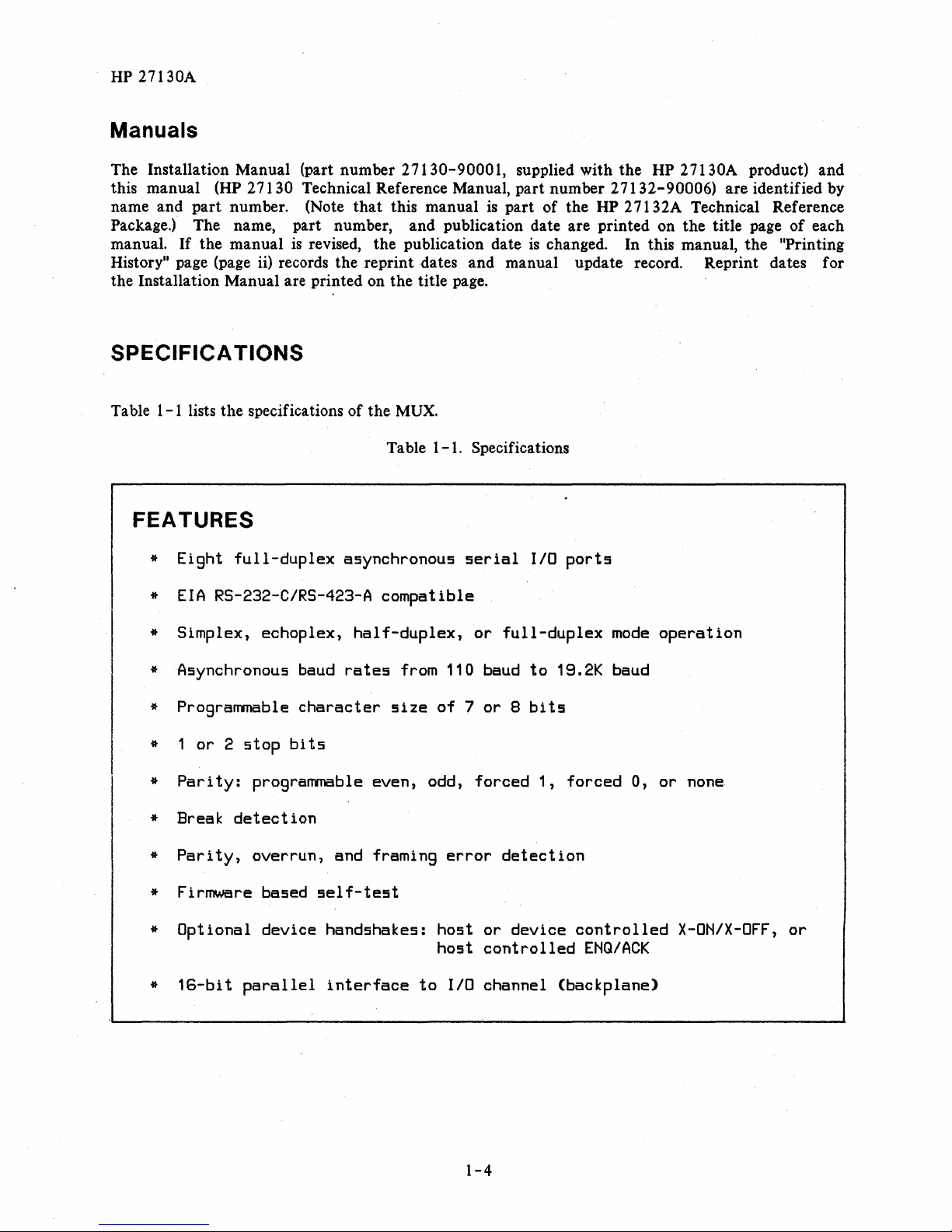
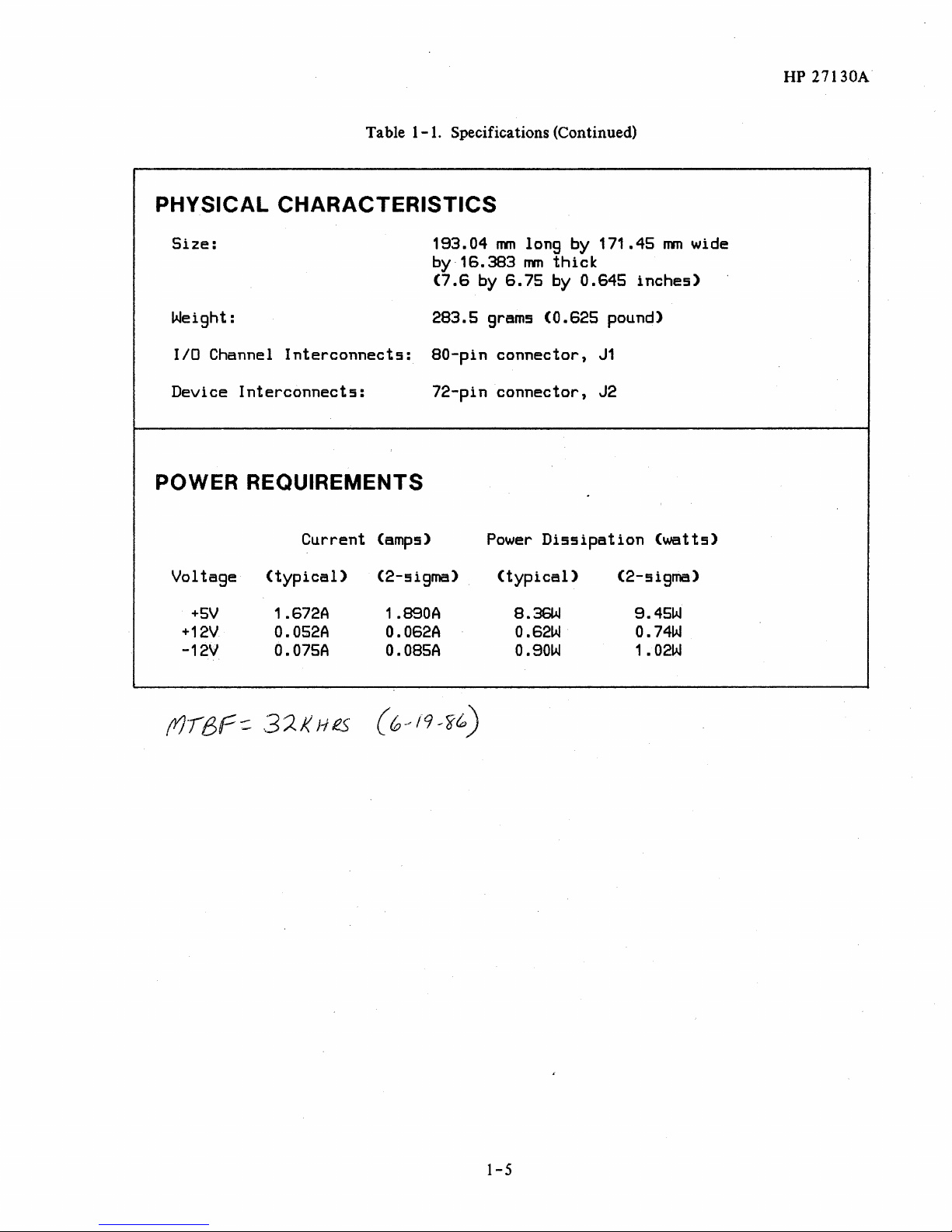
Table 1-1 lists the specifications of the MUX.
27130
number. (Note
Technical Reference Manual,
is
revised, the publication date
TIONS
that
27130-90001,
this manual
Table 1-1. Specifications
supplied with the HP 27130A product) and
part
number
is
part
of the HP 27132A Technical Reference
is
changed. In this manual, the "Printing
27132-90006)
are identified by
of
each
FEATURES
*
*
Eight
EIA
full-duplex
RS-232-C/RS-423-A
asynchronous
compatible
serial
lID
ports
*
Simplex,
echoplex,
* Asynchronous baud
* Programmable
* 1
or 2 stop
*
Parity:
* Break
*
Parity,
detection
* Firmware
*
Optional
*
16-bit
parallel
character
bits
programmable
overrun,
based
device
self-test
handshakes:
half-duplex,
rates
size
even,
and
framing
interface
or
full-duplex
from 110 baud
of 7 or 8 bits
odd,
to
error
host
host
lID
forced
detection
or
device
controlled
channel
to
19.2K baud
1,
forced
controlled
ENQ/ACK
(backplane)
mode
0,
operation
or
none
X-ON/X-OFF,
or
1-4
HP 27130A
PHYSICAL
Table
CHARACTERISTICS
1-1.
Size:
Weight:
lID Channel
Device
Interconnects:
Interconnects:
POWER REQUIREMENTS
(amps)
(2-sigma)
Voltage
Current
(typical)
Specifications (Continued)
193.04
by·
(7.6
283.5
80-pin
72-pin
mm
16.383
by
6.75
grams
connector,
connector,
Power
long by
mm
thick
by
0.645
(0.625
Dissipation
(typical)
171.45
inches)
pound)
J1
J2
(2-sigma)
mm
wide
(watts)
+SV
+12V
-12V
1.672A 1 .890A 8.36W
0.052A
O.075A
O.062A
O.08SA
O.62W
O.90W
9.4SW
0.74W
1.02W
1-5

INSTALLATION 1-
~----------------~[[]
This section provides information on installing and checking
the
operation
of
the
MUX.
DETERMINING CURRENT REQUIREMENTS
The MUX circuit card obtains its operating voltages from the host computer> power supply
the
I/O
channel. Before installing
will overload
requirements
the
appropriate Technical Reference Manuals.
FIRMW
entry
ARE
the
power supply. The
of table
(EPROM) INST ALLA TION
SOME OF THE COMPONENTS USED IN THIS
PRODUCT
STATIC DISCHARGE. REFER TO THE SAFETY
CONSIDERATIONS INFORMATION
FRONT
THE CARD
COMPONENTS.
the
card,
it
is
necessary
current
1-1.
Current
I
ARE SUSCEPTIBLE TO DAMAGE
OF
THIS MANUAL BEFORE HANDLING
OR REMOVING OR REPLACING
requirements
requirements for all
CAUTION
to
determine whether
of
the
I
AT THE
card
other
are
I/O
BY
the
listed
cards
added curre,nt
in
the
can
be found
through
power
in
The EPROMs are installed
that
they are installed properly, and
kets during shipping
..
in
sockets provided on
that
they have
the
MUX card as shown
not
been damaged
2-1
in
figure
or
loosened from
2-1.
Ensure
their
soc-
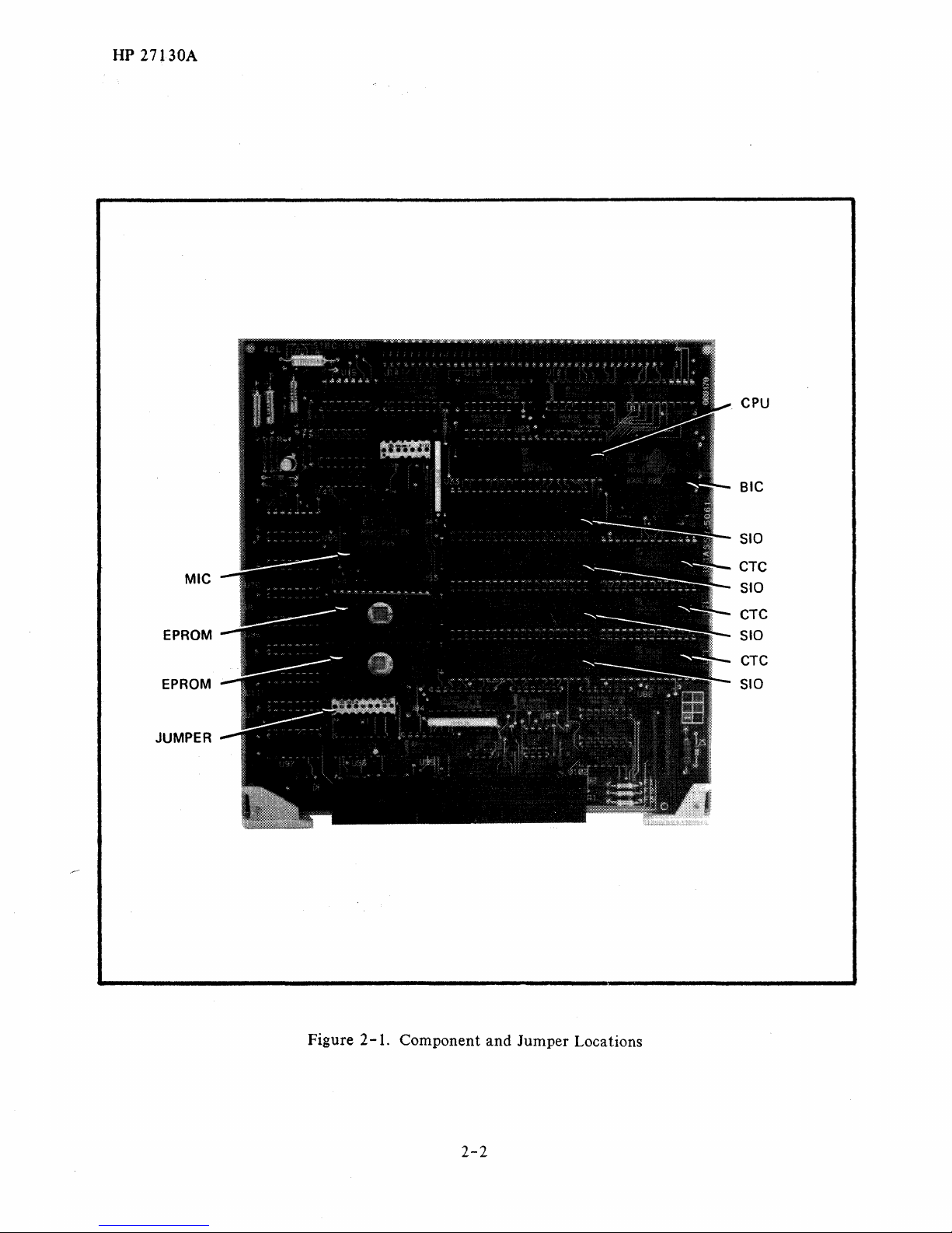
HP 27130A
CPU
SIC
MIC
EPROM
EPROM
JUMPER
SID
CTC
SID
CTC
SID
CTC
SID
Figure
2-1.
Component and Jumper Locations
2-2
HP
27130A
Additionally, when installing or removing EPROMs, guard against bending or breaking
the component. These pins also can become folded between
would result in
straightened
intermittent
with
careful use of needle-nose pliers.
operation of
the
MUX. In most cases, a bent or damaged pin
the
component and its socket, which
the
pins on
can
be
JUMPERS
There are two jumpers on the MUX card: a Memory Configuration jumper, and a Signature Analysis
jumper. The locations of these two jumpers are shown on figure
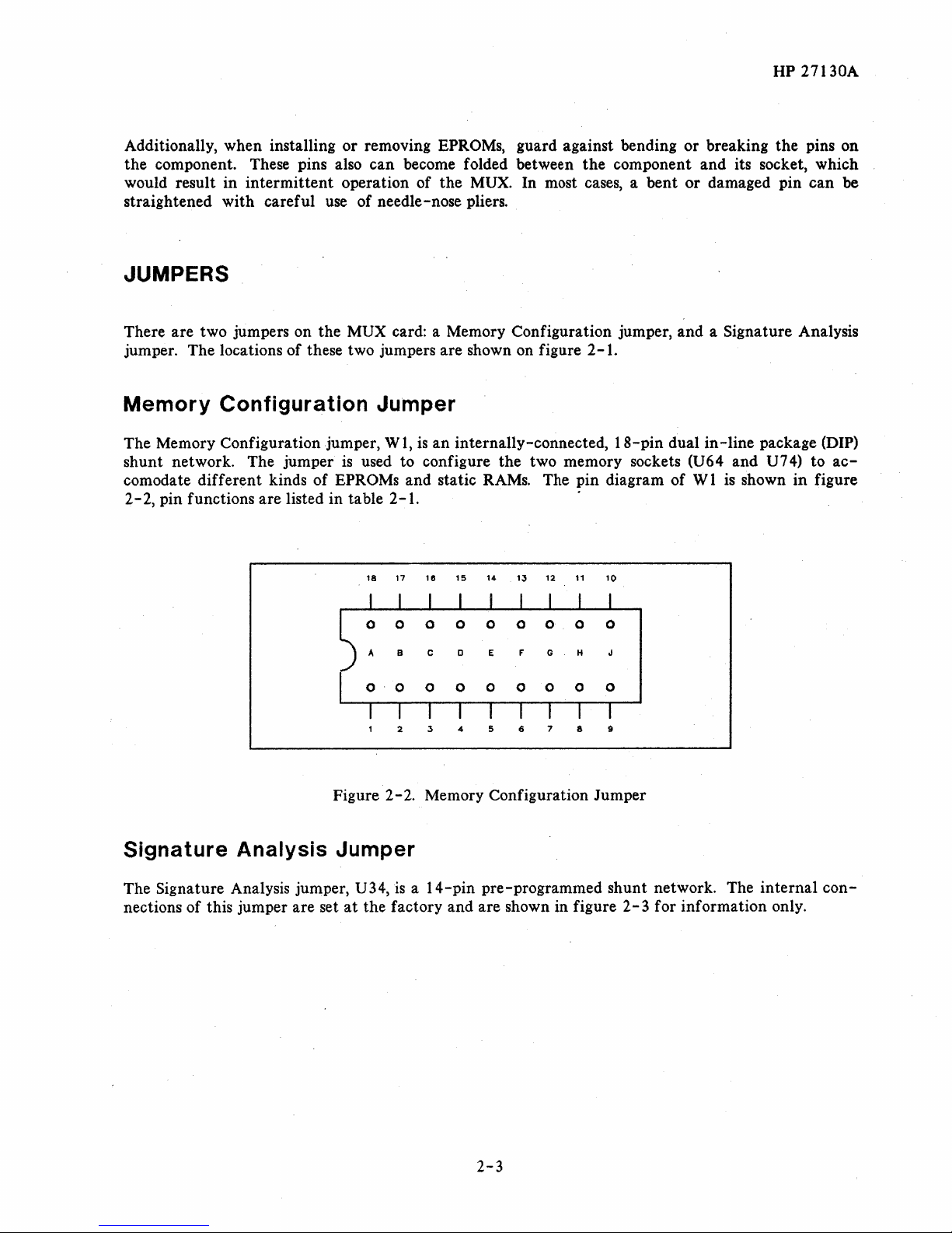
Memory
The Memory Configuration jumper,
shunt network. The
Configuration Jumper
WI,
is
an
jumper
is
used to configure the two memory sockets (U64 and U74) to
internally-connected,
comodate different kinds of EPROMs and static RAMs. The pin diagram of
2-2,
pin functions are listed in table
18
2-1.
17
18
15
14
13
12
11
2-1.
10
IS-pin
dual
in-line
WI
package (DIP)
is
shown in figure
ac-
234
Figure
2-2.
Signature Analysis Jumper
The Signature Analysis jumper, U34,
nections of this jumper are set
at
is a I4-pin
the factory and are shown in figure
567
8 9
Memory Configuration Jumper
pre-programmed shunt network. The
2-3
2-3
internal
for information only.
con-
HP
27130A
Table
2-1.
Functions of the Memory Configuration Jumper
JUMPER
A
B
C
D
E
Installed
Position
to
pin
20
EPROM
in
addressed.
Installed
Position
byte
which
in
EPROM
EPROM
socket
addressed.
Installed
Position
EPROM.
Installed
Position
the
16K
byte
Installed
Position
EPROM.
only
A
connects
(CE-)
socket
only
B
connects
or
pin
is
U64
only
C
connects
only
D
connects
EPROM.
only
E
connects
FUNCTION
when a 16K
OCE2-
of
the
EPROM
U64
whenever
when a 4Kor
OCEO-
20
(CE-)
installed
whenever
when a 4K
byte
+5V
when a 16K
A13
when
an
8K
+5V
byte
of
8K
of
of
in
socket
the
power
byte
of
byte
power
EPROM
the
in
socket
the
byte
the
the
lower
EPROM
EPROM
the
EPROM
Memory
lower
EPROM
MIC
8K
byte
U64.
8K
to
pin
address
to
pin
is
used
Interface
U64.
16K
is
to
pin
This
bytes
is
used
24
is
used
bus
is
used
27
in
This
bytes
used
18 (CE-)
EPROM,
enables
of
in
(VDD)
in
to
pin
in
(VPP-)
socket
Circuit
U64.
(MIC)
enables
of
in
memory
socket
of
are.
U64.
the
depending on
the
EPROM
memory
socket
of
socket
the
4K
are
U64.
byte
U64.
24 (A13)
socket
of
the
8K
U74.
byte
the
4K
of
F
G
H
J
Installed
Position
static
Installed
Position
static
Installed
RAM
is
CPU
address
byte
RAM,
Installed
(access
only
F
RAM,
only
G
RAM,
only
used
depending
to
time
when
connects
thus
enabling
when a 2K
connects
thus
enabling
when a 4K
in
socket
bus
to
pin
enable
greater
an
8K
WR-
WR-
U74.
23 (A11)
on
the
than
byte
of
the
byte
of
the
or
8K
the
CPU
static
the
CPU
static
Z-80~
Z-80B
byte
to
write
RAM
to
write
EPROM
RAM
CPU
CPU
Position H connects
of
the
which
MIC
250
device
wait
nsec)
is
state
are
2-4
is
to
to
is
used
to
to
or
4K
or
installed
signal
used
used
pin
the
pin
the
an
8K
when
in
in
27
RAM.
in
21
RAM.
8K
A11
byte
in
U64
socket
(WE-)
of
socket
(WE-)
byte
of
of
static
the
EPROM
~ocket
slow
or
EPROMs
U74.
U74.
the
U74.
the
Z-80B
or
8K
U74.

1"
13
12
11
2 3 " 5 S 7
10
HP
27130A
a
Figure 2-3.
1/0
CHANNEL INTERFACE
All interface between
nector
(J
1)
located on
are listed in table
2-2.
the
the
MUX
Signature Analysis Jumper Internal Connections
and
the host computer occurs on
MUX mates with a receptacle on
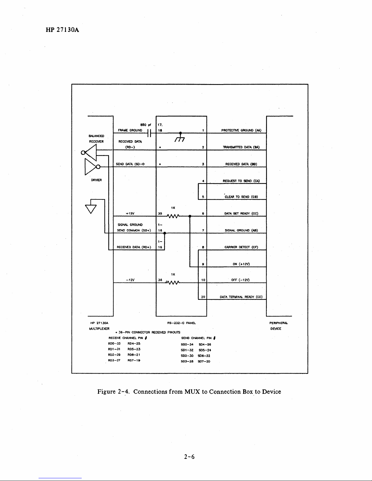
PERIPHERAL DEVICE INTERFACE
Interface between
to a connection panel
eight separate connectors and eight cables, to
connection box
Connector
J2
tion panel are shown
and Signal Ground
is,
one pair
(JO
through J7) to
of
the
MUX card and up to eight peripheral devices
(RS-232-C
is
shown
in
figure 2 -
pin assignments
in
table
(SG)
lines, and eight pairs of Receive
Send
Data
lines
the
eight peripheral devices.
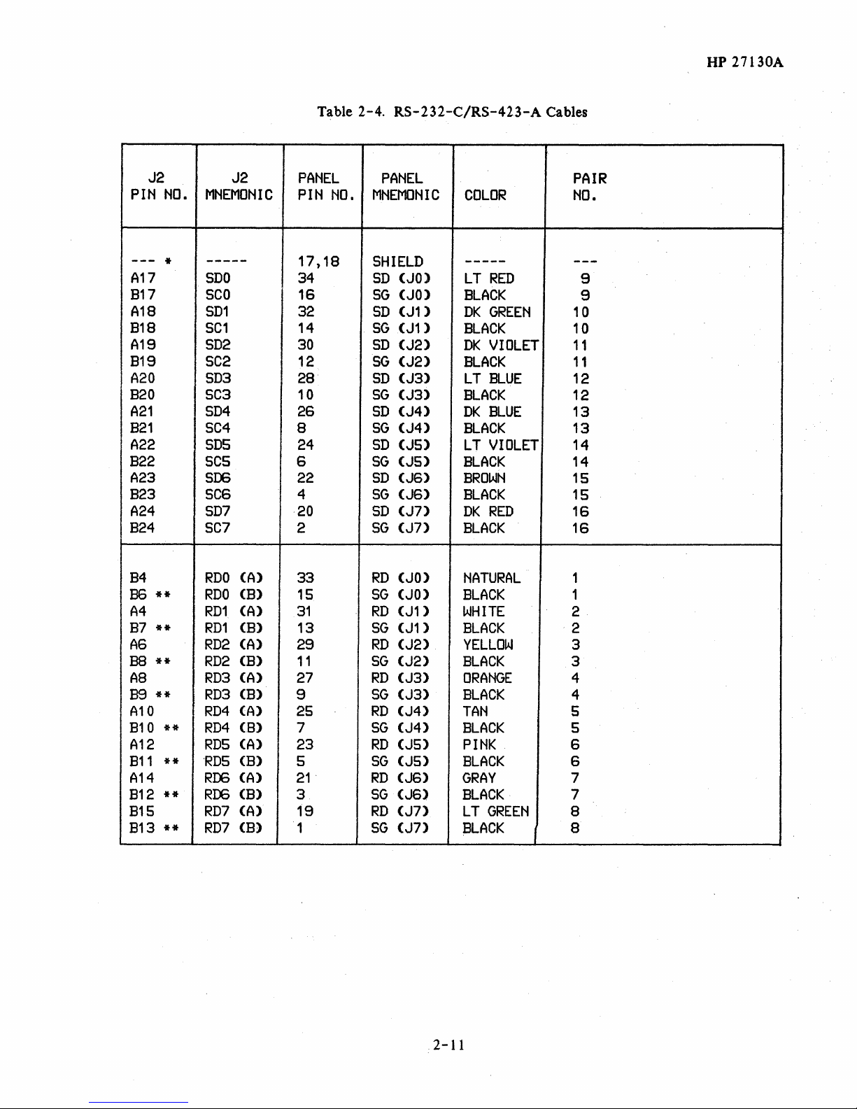
Connection
Box,
the
4.
are
shown in table
2-4.
Note that, in table
and
one pair of Receive Data lines for each
the
I/O
part
the
number
channel. An
I/O
channel. Connections to J 1
is
via a
12828-60001)
72-pin
and from there, via
80-pin
connector (J2)
peripheral devices. A connection diagram for
2-3.
Pin assignments for
2-4,
there
are eight pairs
Data
(RD)
and
Signal
J2
and
of
Ground
of
the
the
connec~
Send
(SG)
Data
lines;
eight connectors
con-
the
(SD)
that
2-5
HP 27130A
BALANCED
RECEIVER
~
~
'-
DRIVER
FRAME
RECEIVED
SEND
GROUND
(RD-)
MTA
MTA
(50-0
850
pf
17.
,.
II
II
1
PROTECTIVE
GROUND
(M)
m
.
.
2
:5
4
~
TRAN5MIlTED
RECEIVED
REQUEST
TO
CLEAR
TO
OATA
DATA
SEND
SEND
(SA)
(89)
(CA)
(ca)
7
HP 271JOA
MVLTlPLEXER
•
RECEIVE
RDO-JJ
R01-J1
RD2-29
ROJ-27
+12'V
SIGNAL
SEND
COMMON
RECEIVED
-12V
36-PIN
CH.',NNEL
R04-2~
RD5-23
RD6-21
R07-1~
GROUND
(SO+)
OATA
(RD+)
CONNECTOR
PIN
1K
35
AAAA.
yyy
1-
111
1-
16 8
lK
36
~AA'"
yyy
R5-232-C
RECEIVED
PINOUTS
I
PANEL
SEND
500-34
501-32
SD2-3O
503-28
CHoINNEl
S04-26
505-24
506-22
SD7-20
o.t.TII
SET
AEADY
6
7
9
10
20
PIN
OATA
*
SIGNAL GROUND
CARRIER
ON
OFF
TERt,lINAL
(CC)
(,t,B)
OETECT(CF)
(+12V)
(-12\0
READy
(CO)
PERIPHE:I'W.
DEVICE
Figure 2-,4. Connections from MUX to Connection
2-6
Box
to Device
HP 27130A
PIN
A1
A2
A3
A4
AS
A6
A7
A8
A9
A10
A11
A12
A13
A14
A15
A16
A17
A18
A19
A20
A21
A22
A23
A24
A25
A26
A27
A28
A29
A30
A31
A32
A33
A34
A35
A36
A37
A38
A39
A40
NO.
SIGNAL
RES
DB14DB12GND
DB10DBBGND
DB6DB4GND
DB2DBOGND
AD2ADOGND
DOUTBPOCENDSYNCGND
CCLK
GND
BRDBYTMYADGND
---
---
---
RES
PFWPPON
GND
ACAC+
-12+12
+5S
+5P
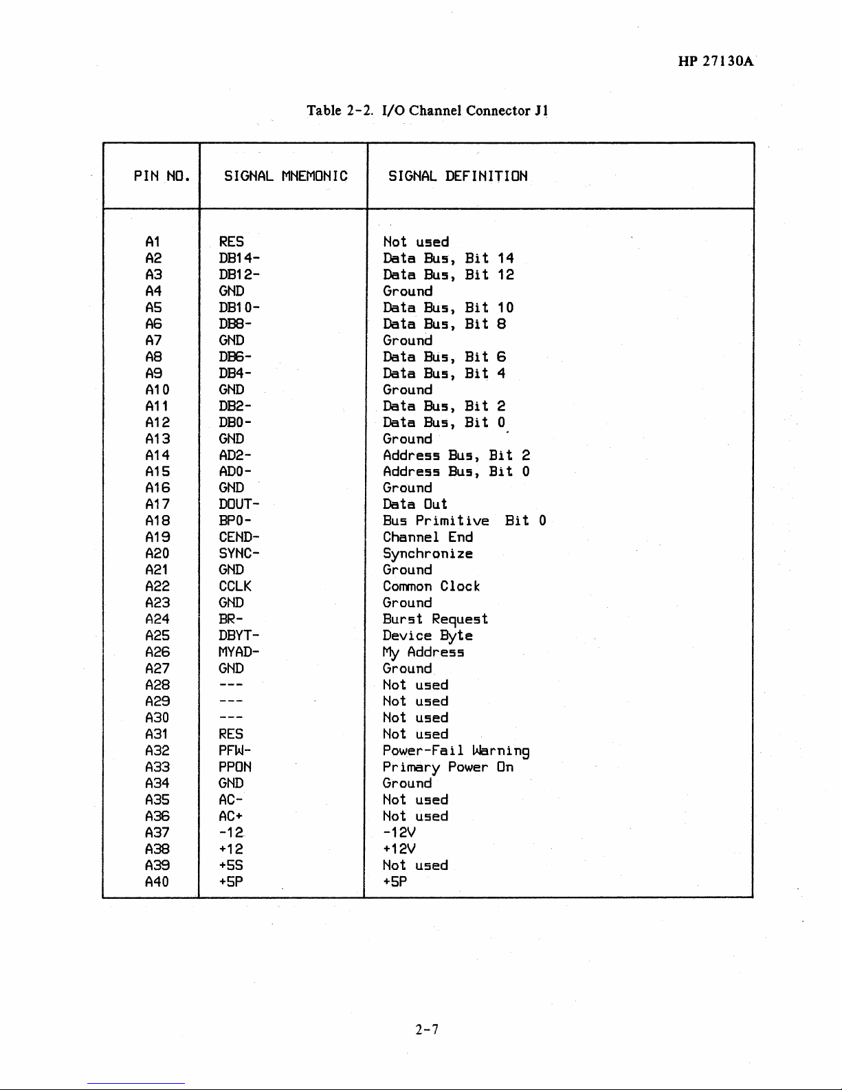
Table 2-2.
MNEMONIC
I/O
Channel Connector
SIGNAL
Not
Data Bus,
Data Bus,
DEFINITION
used
Bi
Bit
Ground
Data Bus,
Data Bus,
Bi t 10
Bit
Ground
Data Bus,
Data Bus,
Bit
Bit
Ground
Data Bus,
Data Bus,
Bit
Bit
Ground
Address Bus,
Address Bus,
Ground
Data
Bus
Channel
Out
Primitive
End
Synchronize
Ground
Corrmon
Clock
Ground
Burst Request
Device Byte
My
Address
Ground
Not
used
Not
used
Not
used
used
Not
Power-Fail
Primary
Warning
Power
Ground
Not
used
Not
used
-12V
+12V
Not
used
+5P
t
Bi
Bit
14
12
8
6
4
2
0
t
Bit
On
Jl
2
0
0
2-7
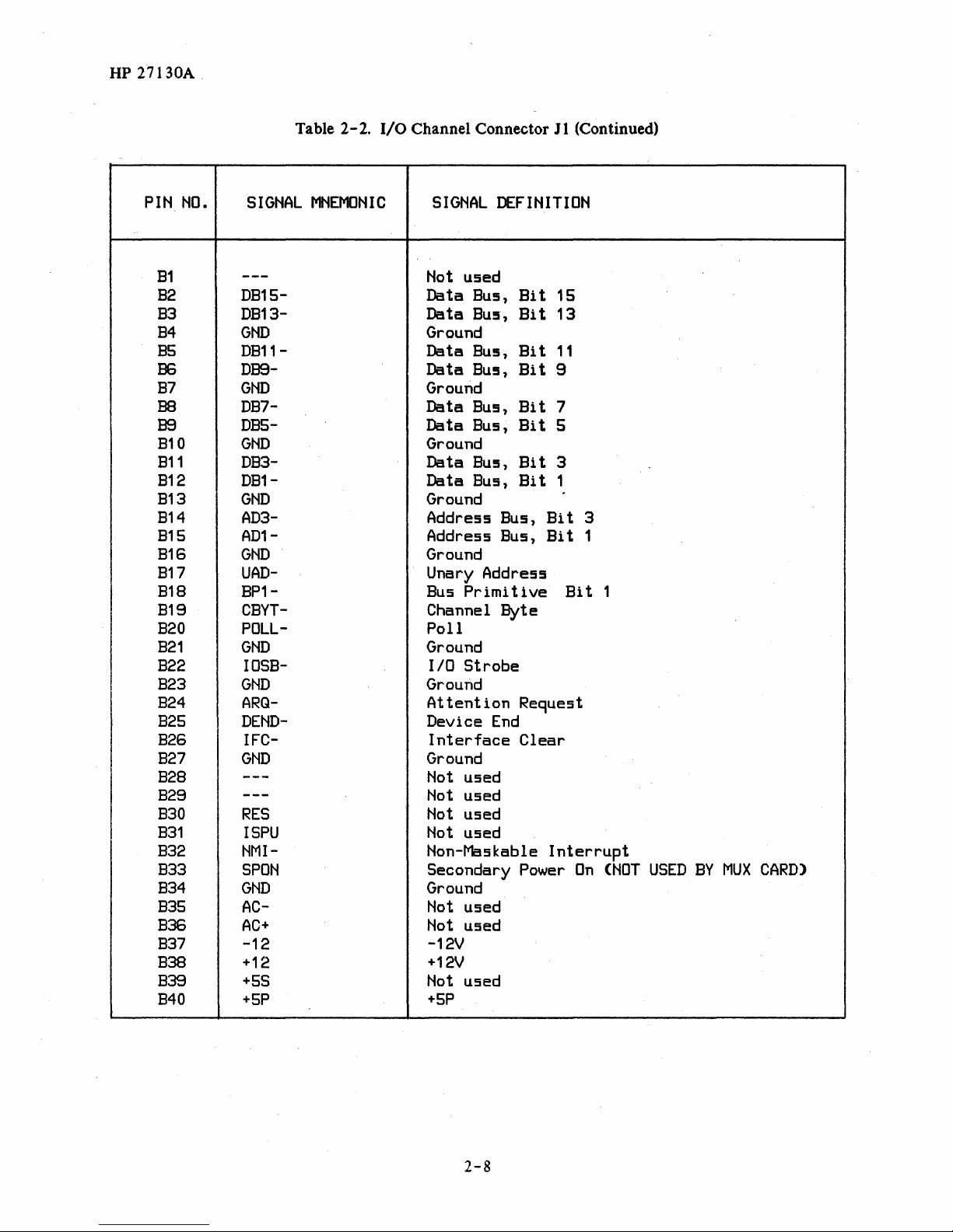
HP 27130A .
PIN
NO.
B1
B2
B3
B4
B5
B6
B7
B8
BS
B10
B11
B12
B13
B14
B15
B16
B17
B18
B19
B20
B21
B22
B23
B24
B25
B26
B27
B28
B29
B30
831
832
B33
834
835
836
B37
838
839
B40
5 I
GNAL
---
DB15DB13GND
DB11DBSGND
DB7DB5-
GND
DB3DB1GND
AD3AD1GND
UADBP1CBYTPoLLGND
10SBGND
ARQDEND-
IFC-
GND
---
---
RES
ISPU
NMISPoN
GND
ACAC+
-12
+12
+55
+5P
Table
2-2.
MNEMON
I/O
Channel Connector
I C
SIGNAL
Not
Data Bus,
Data Bus,
Ground
Data Bus,
Data Bus,
Ground
Data Bus,
Data Bus,
Ground
Data Bus,
Data Bus,
Ground
Address Bus,
Address Bus,
Ground
Unary Address
Bus
Channel Byte
Poll
Ground
lID
Ground
Attention
Device
Interface
Ground
Not
Not
Not
Not
Non-Maskable
Secondary
Ground
Not
Not
-12V
+12V
Not
+5P
DEFINITION
used
Bit
Bit
Bit
Bit
Bit
Bit
Bi
Bi
Primitive
Strobe
Request
End
Clear
used
used
used
used
Power
used
used
used
Jl
(Continued)
15
13
11
9
7
5
t 3
t
1
Bit
3
Bit
1
Bit
Interrupt
On
1
(NOT
USED
BY
MUX
CARD)
2-8
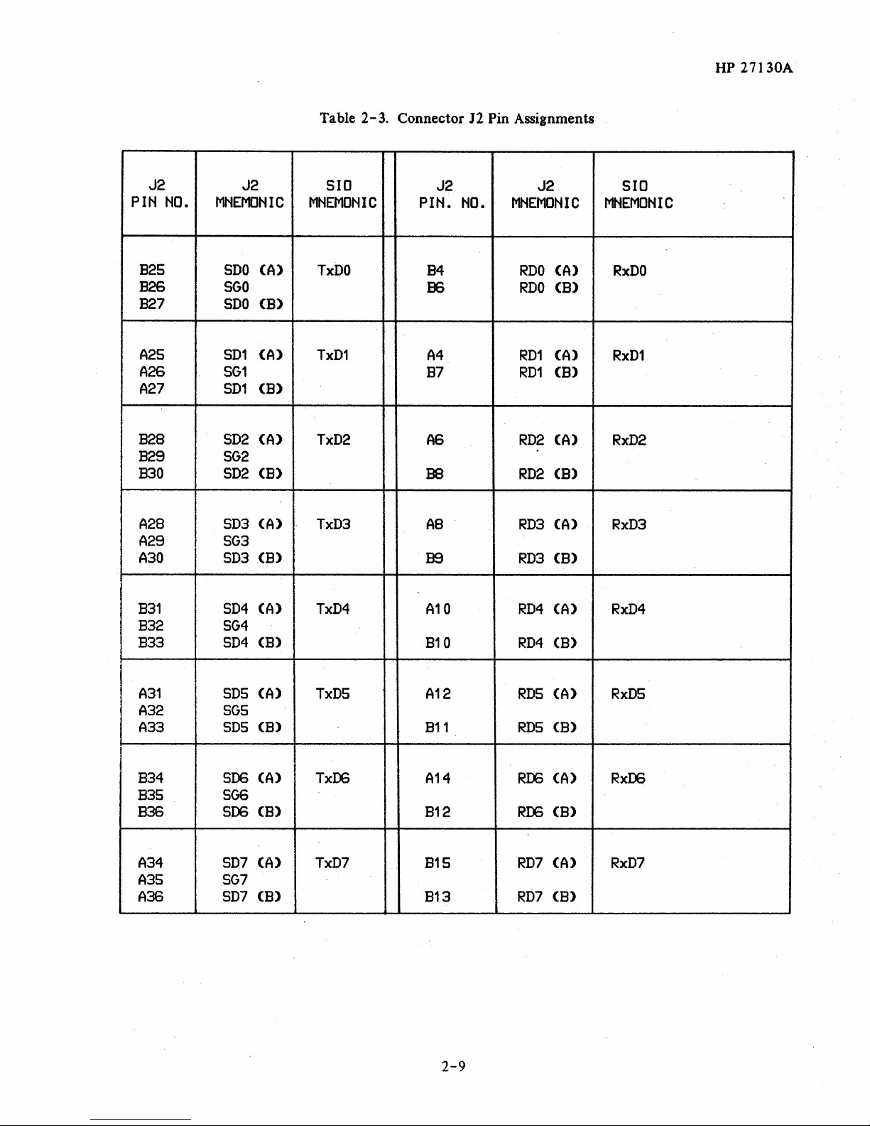
Table
2-3.
Connector J2 Pin Assignments
HP 27130A
J2
PIN
B25
B26
B27
A25
A26
A27
B28
B29
B30
A28
A29
A30
NO.
J2
MNEMONIC
SDO
CA)
SGO
CB)
SDO
CA)
SD1
SG1
CB)
SD1
SD2
CA)
SG2
SD2
CB)
SD3
CA)
SG3
SD3CB)
SIO
MNEMONIC
TxDO
TxD1
TxD2
TxD3
J2
PIN.
B4
136
A4
B7
AS
B8
A8
B9
NO.
J2
MNEMONIC
CA)
RDO
CB)
RDO
CA)
RD1
CB)
RD1
RD2
CA)
RD2
CB)
RD3
CA)
RD3
CB)
SIO
MNEMONIC
RxDO
RxD1
RxD2
RxD3
B31
B32
B33
A31
A32
A33
B34
B35
B36
A34
A35
A36
SD4
SG4
SD4
SD5
SG5
SDS
SDG
SGS
SOO
SD7
SG7
SD7
CA)
CB)
CA)
(8)
CA)
(8)
CA)
CB)
TxD4
TxD5
TxOO
TxD7
A10
810
A12
811
A14
B12
B15
813
RD4
RD4
RD5
RDS
ROO
ROO
RD7
RD7
CA)
(8)
CA)
(8)
CA)
CB)
CA)
(8)
RxD4
RxD5
RxOO
RxD7
2-9
HP 27130A
J2 J2
PIN
NO.
A17
B17
A1B
B1B
A19
B19
A20
B20
MNEMONIC
SDO
SCO
SD1
SC1
5D2
5C2
5D3
5C3
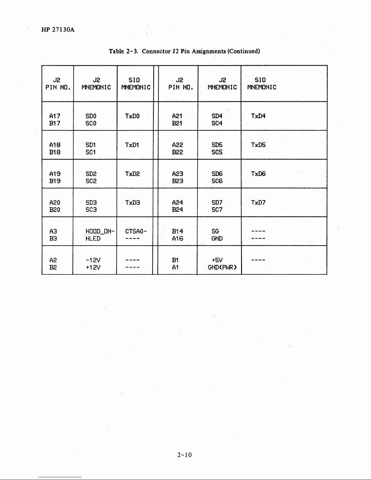
Table 2-3.
SIO
MNEMONIC
TxDO
TxD1
TxD2
TxD3
Connector
J2
Pin Assignments (Continued)
J2 J2
PIN
A21
B21
A22
B22
A23
B23
A24
B24
NO.
MNEMONIC
SD4
SC4
SDS
SCS
500
5C6
5D7
SC7
SIO
MNEMONIC
TxD4
TxDS
TxOO
TxD7
A3
B3
A2
B2
HOOD_ONHLED
-12V
+12V
CT5AO-
----
----
----
B14
A16
B1
A1
SG
GND
+SV
GND(PWR)
----
----
----
2-10
HP 27130A
J2
PIN
--A17
B17
A18
B18
A19
B19
A20
B20
A21
B21
A22
B22
A23
B23
A24
B24
NO.
*
J2
MNEMONIC
-----
SDO
SCO
SD1
SC1
SD2
SC2
SD3
SC3
SD4
SC4
SD5
SC5
SOO
SC6
SD7
SC7
Table 2-4.
PANEL
PIN
NO.
17,18
34
16
32
14
30
12
28
10
26
8
24
6
22
4
20
2
RS-232-C/RS-423-A
PANEL
MNEMONIC
SHIELD
SD
(JO)
SG
(JO)
SD
(J1)
SG(J1)
SD
(J2)
SG
(J2)
SD
(J3)
SG
(J3)
SD
(J4)
SG
(J4)
SD
(J5)
SG
(J5)
SD
(J6)
SG
(J6)
SD
(J7)
SG
(J7)
COLOR
-----
LT
BLACK
DK
BLACK
DK
BLACK
LT
BLACK
DK
BLACK
LT
BLACK
BROWN
BLACK
DK
BLACK
RED
GREEN
VIOLET
BLUE
BLUE
VIOLET
RED
Cables
PAIR
NO.
---
9
9
10
10
11
11
12
12
13
13
14
14
15
15
16
16
B4
B6
A4
B7
A6
B8
A8
B9
A10
B10
A12
B11
A14
B12
B15
B13
**
**
**
**
**
**
**
**
RDO
RDO
RD1
RD1
RD2
RD2
RD3
RD3
RD4
RD4
RD5
'RD5
ROO
ROO
RD7
RD7
(A)
(B)
(A)
(B)
(A)
(B)
(A)
(B)
(A)
(8)
(A)
(8)
(A)
(B)
(A)
(B)
33
15
31
13
29
11
27
9
25
7
23
5
21
3
19
1
RD
SG
RD
SG
RD
SG
RD
SG
RD
SG
RD
SG
RD
SG
RD
SG
(JO)
(JO)
(J1)
(J1)
(J2)
(J2)
(J3)
(J3)
(J4)
(J4)
(J5)
(J5)
(J6)
(J6)
(J7)
(J7)
NATURAL
BLACK
WHITE
BLACK
YELLOW
BLACK
ORANGE
BLACK
TAN
BLACK
PINK
BLACK
GRAY
BLACK
LT
GREEN
BLACK
1
1
2
2
3
3
4
4
5
5
6
6
7
7
8
8
2-11
HP
27130A
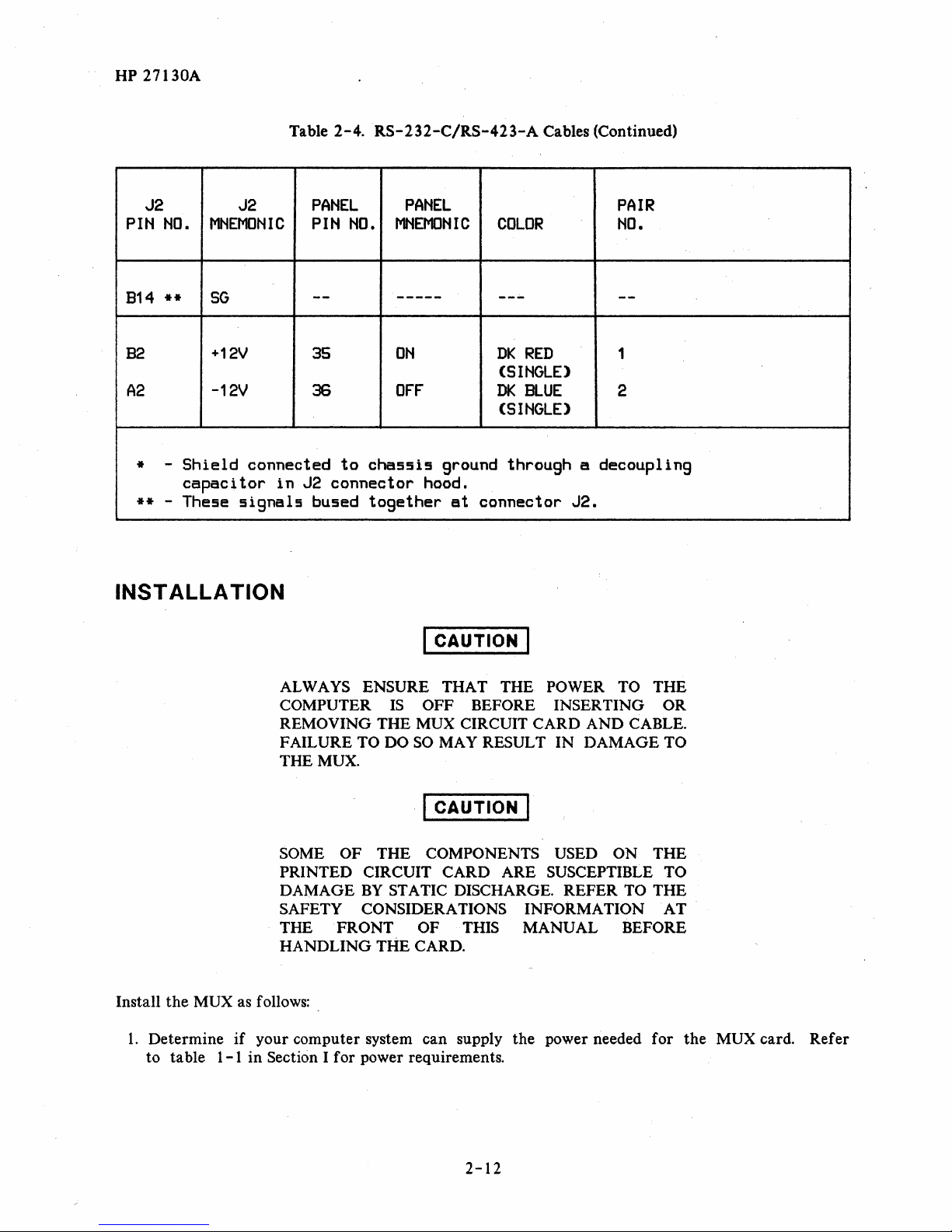
Table
2-4.
RS-232-C/RS-423-A
Cables (Continued)
J2 J2
PIN
NO.
B14
**
B2
A2
-
Shield
*
capacitor
- These
**
INST
ALLA
MNEMONIC
SG
+12V
-12V
connected
in
J2 connector hood.
signals
TION
PANEL
PIN
NO.
--
35
36
to
bused
PANEL
MNEMONIC
-----
ON
OFF
chassis
together
I CAUTION I
PAIR
COLOR
---
DK
RED
NO.
--
1
(SINGLE)
DK
BLUE
2
(SINGLE)
ground through a decoupling
at
connector
J2.
Install
1.
Determine
to table
the
MUX as follows:
if
1-1
ALWAYS ENSURE THAT THE POWER TO THE
COMPUTER
REMOVING THE MUX CIRCUIT CARD AND CABLE.
FAILURE
THE MUX.
IS
TO DO
OFF BEFORE INSER TING OR
SO
MAY RESULT IN DAMAGE TO
I CAUTION I
SOME OF THE COMPONENTS USED ON THE
PRINTED CIRCUIT CARD ARE SUSCEPTIBLE TO
DAMAGE
SAFETY CONSIDERATIONS INFORMATION
THE
HANDLING
your computer system
in
Section I
BY
STATIC DISCHARGE. REFER TO THE
FRONT
for
power requirements.
OF THIS MANUAL BEFORE
THE CARD.
can
supply
the
power needed
AT
for
the
MUX card. Refer
2-12
2.
Verify
installed on the card. To verify
EPROMs/RAMs
correct jumpers are closed.
3.
Install
stallation manual
damage components or traces on the card or on adjacent cards. Press
place.
4.
Connect
have the test hood, which exercises more
(Hewlett-Packard
that
the Memory Configuration jumper
that
are
installed in sockets U64 and U74, then
the
card in
the
the
appropriate slot in
to
determine
cable supplied with the card from
part
number 0950-1659), connect
BE
SURE AND INSTALL THE DIAGNOSTIC TEST
HOOD
WITH THE LED) MATCHES THE COMPONENT SIDE
ON
CARD CAN RESULT IF THE COMPONENT SIDES OF
THE TWO DEVICES DO NOT MATCH.
SO
THE MUX CARD. DAMAGE TO THE MUX
the
THAT
is
configured correctly for
the jumper
correct slot. When installing
I
CAUTION
ITS
COMPONENT SIDE (THE SIDE
is
configured correctly, determine
the
computer. Refer
J2
of
the
it
I
refer
to the
to J2 instead
RS-232-C
card's circuitry, and
to
table
to
the
the
the
of
connecting
UP 27130A
the
EPROMs/RAMs
what
types
2-1
to verify
computer system
card, use
MUX card firmly into
connection
can
the
that
the
in-
c,are
not
box.
If
you
be ordered
cable.
of
to
START-UP
To start up and verify correct operation of the
1.
Turn
on computer system power.
2.
A self
-test
is
contained on the card. The host computer system determines
run
automatically
manual for your system for a description of self
a.
If
the diagnostic test hood
card should light briefly and
does not light
test. For either of these
to Hewlett-Packard; refer to the next paragraph for reshipment information.
perform maintenance on the card, however,
formation, replaceable parts lists, and schematic logic diagrams, respectively.
b.
If
the
diagnostic test hood
should occur, plus the LED located on the test hood should light briefly and
LEOs (the one
or
if
they light and stay on, the causes are the same as in step
3.
Refer to your system documentation for information on using
at
power-on or must be invoked
is
not installed when
go
at
all, the card
latter
moun~ed
on the card and the one on the diagnostic test hood)
two cases,
is
installed
MUX, perform
-test
the
out. This indicates
is
defective.
wh~n
it
refer
If
the LED stays on,
is
recommended
to Sections
the
self-test executes,
by
initiation.
self
that
the
following:
the
user. Refer
-test
executes,
the card passed self-test.
V,
VI,
2.a.
the
LED located on
the
card did not pass
that
you
and VII for maintenance
the
conditions in step
the
MUX in your system.
if
to
the
return
If
do
the
self
-test
appropriate
If
the LED
the
you wish to
go
out.
If
not light
at
is
the
self-
card
in-
2.a.
the
all,
2-13
HP 27130A
RESHIPMENT
If
the MUX
owner and indicating the reason for shipment. Include the
is
to
be
shipped
to
Hewlett-Packard for any reason,
part
number of the
attach
a tag identifying the
MUX.
Pack the card in the original factory packing material,
available, good commercial packing
material-should be used. Reliable commercial packing and ship-
if
available.
ping companies have the facilities and materials to repack the item.
ANTI-STATIC PRECAUTIONS.
If
the original material
BE
SURE TO OBSERVE
is
not
2-14
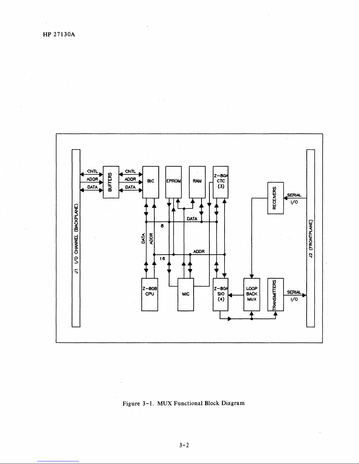
PRINCIPLES OF OPERA TION 1-
~------------------~~
FUNCTIONAL DESCRIPTION
A functional block diagram of the HP 27130 Eight-Channel Multiplexer is shown in figure
3-1. Reference will also be made to the schematic logic diagram contained in Section
Note
that
figure
C23,
7-1;
D37,
bination of letters A through E and numbers
on the individual sheets; and
7-1
consists of five sheets. References to this figure will be as follows:
7-1,
etc., where the first digit (1,
7-1
refers to
2,
3,
4,
or
5)
refers
11
through
the
figure number. For example,
58
(All,
to
the
D37, etc.)
sheet number;
refer
VII, figure
All,
the
to
the
quadrants
7-1.
7-1;
com-
r
A11
L
Circuitry contained on
its support circuits, a
four Z-80 Serial
Interface Circuit (MIC) gate array, 64K bytes of dynamic RAM (48K available)
RS-422-A/RS-423-A
I/O
channel (backplane) and peripheral device panel (frontplane) connectors.
The
heart
in
EPROM controls
The Backplane Interface Circuit
circuit which controls
The
BIC
Memory Access (DMA) for data transfer to memory.
The Counter Timer Circuits (CTC,
provide baud
CPU
as
I/O
quadrant
sheet
of
is
1
the
accessed by
rate
devices.
r
D37
L
the
MUX card includes a Backplane Interface Circuit
Z-SOB microprocessor (CPU), three
I/O
circuits (SI0/2s), up to 16K bytes of EPROM in two
transmitters and receivers (compatible
MUX card
the
clocks and other necessary clocks for the
is
the Z-SOB CPU (U33,
functions of the card.
(BIC,
the
communication and handshaking with
the
Z-SOB CPU as
U51, U61, and U71,
sheet
U41,
quadrant
3
see
A14, 7-1)
an
I/O
device for control information, and through Direct
Z-80
with
see
D24, 7-1), which through a program stored
is
see
MUX.
(BIC)
Counter Timer Circuits
28-pin
RS-232-C
a custom gate
the
I/O
E43,
7-1)
divide
They are accessed by
sockets, a Memory
and CCITT
array
channel (backplane).
the
gate
array
integrated
system clock to
the
(CTCs),
V.2S),
Z-80B
and
and
The Memory Interface Circuit
which handles dynamic refresh and address multiplexing for
MIC also contains
decodes addresses and provides wait states for
rest of the MUX card.
Serial 1/ 0 circuits
The
plexers, receivers, and drivers
frontplane connector J2.
the
(SIOs,
PMA
(MIC,
U 4
(see
U54, see A32,
controller, provides
3,
U 5
3,
U 63 and U 73,
figure 7
-1,
7-1)
is
a custom gate
the
64K bytes of dynamic RAM. The
interrupt
the
slow EPROMs, and provides reset for
see
sheet
5),
provide serial data communication to
3-1
vectors for backplane interrupts,
A 4
2, 7 -1)
and
array
their
integrated circuit
the
for
the
associ a ted m ul
ti
the
-
HP
27130A
·0
Q
~
a.
~
~
-
..J
~
z
~
0
g
....
..,
~
~
a::
0
~
8
16
DATA
AIlOR
~
~
LA.!
0
LA.!
0::
SERIAL
I/O
,....
IAJ
S
/l.
~
~
II..
'-"
C'4
""J
Figure
Z-80B
<:PU
3-1.
MUX Functional Block Diagram
3-2
SERIAL
I/o
HP 27130A
System
Three synchronized system clocks (1.8432 MHz, 3.6864 MHz, and 7.3728 MHz), all derived from
the I 4.7456 MHz clock signal CCLK
1.8432 MHZ
3.6864 MHz
7.3728 MHz
Clocks
(PHI_CTC): Provides
rates
and
system timing intervals.
(PHI):
and
(2_PHI): Drives
Used to provide a system clock to
the
CTCs.
the
+
(see
input
MIC.
A 21, 7
to
the
-1),
perform
CLK/TRGpins
the
following functions:
on
the
CTCs to generate _ baud
the
Z-80B
CPU,
the
SIOs
and MIC,
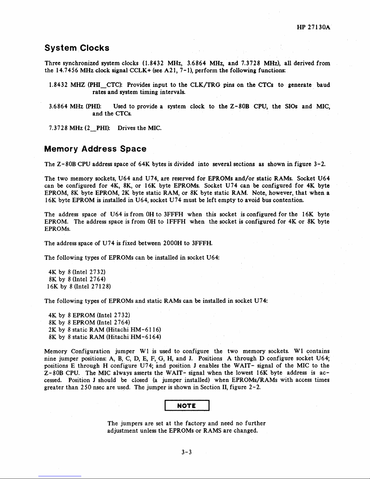
Memory Address Space
The
Z-80B
The two memory sockets, U64 and U74, are reserved for EPROMs
can be configured for 4K,
EPROM,
16K byte
The address space of
EPROM. The address space
EPROMs.
CPU address space of 64K bytes
8K,
or 16K byte EPROMs. Socket U74 can be configured for 4K byte
8K
byte EPROM, 2K byte static RAM, or
EPROM
is
installed in U64, socket U74 must be left empty to avoid bus contention.
U64 is from
is
from
OH
to 3FFFH when this socket
OH
to IFFFH when the socket
is
divided into several sections as shown
and/or
8K
byte static RAM. Note, however,
static RAMs. Socket
is
configured for the 16K byte
is
configured for 4K or 8K byte
in
figure
that
3-2.
U64
when a
The address space
The following types of
4K by 8 (Intel 2732)
8K
by 8 (Intel 2764)
16K by 8 (Intel 27128)
The following types of
4K by 8 EPROM (Intel 2732)
8K
by 8 EPROM (Intel 2764)
2K by 8 static RAM (Hitachi
8K
by 8 static RAM
Memory Configuration jumper WI
nine jumper positions:
positions E through H configure U74; and position J enables
Z-80B
cessed. Position J should be closed
greater
cpu. The MIC always asserts the WAIT- signal when the lowest 16K byte address
than
250
of
U74
is
fixed between 2000H to 3FFFH.
EPROMs can be installed
EPROMs and static RAMs can be installed in socket U74:
HM-6116)
(HitachiHM-6164)
is
used to configure the two memory sockets.
A,
B,
C,
D,
E,
F, G,
(a
nsec are
us~d.
The jumper
in
socket U64:
H,
and
J.
Positions A through D configure socket U64;
jumper installed) when EPROMs/RAMs with access times
is
shown in Section II, figure
NOTE
the
WAIT- signal
2-2.
of
the
WI
contains
MIC to
is
the
ac-
The jumpers are set
adjustment unless
at
the
factory and need no
the
EPROMs or RAMS are changed.
3-3
further
 Loading...