

Page 1

HP
This vintage Hewlett Packard document was
preserved and distributed by
Archive
vvwvv.
Please visit us on the web
Scanned by on-line curator: Tony Gerbic
h parc hive.com
!
**
For
FREE
Distribution Only
***
Page 2
Page 3
OPERATING AND SERVICE MANU'AL
MODEL
SERIALS
PREFIXED:
175A
235
OSCILLOSCOPE
4
-
01526-1
Copyrieh)
1501
PAOt
HtWLtIT-PACKARO COMPANY
MILL
ROAD,
PAL0
ALlO,
0
CALIFORNIA,
1963
U.S.A.
Printed:
FEB
1963
Page 4
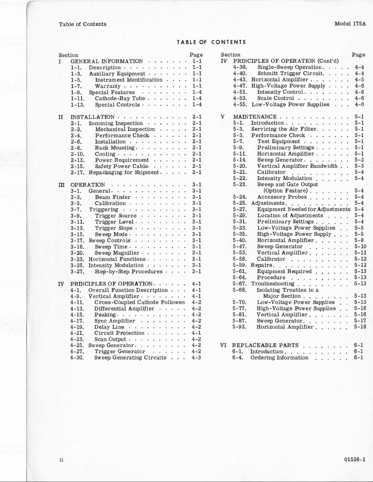
Table of Contents Model 175A
Section
I
GENERALINFORMATION
1.1
.
Description
1.3 . Auxiliary EquipmeQt
1.5
.
Instrument Identification
1.7
.
Warranty
1.9
.
Special Features
1.11
.
Cathode-Ray Tube
1.13
.
Special Controls
I1
INSTALLATION
2.1
.
Incoming Inspection
2.2
.
MechanicalInspection
2.4
.
Performance Check
2.6
.
Installation
2.8
.
Rack Mounting
.
2.10
2.13
2.15
2.17
m
OPERATION
3.1
3.3
3.5
3.7
3.9
3.11
3.13
3.15
3.17
3.18
3.20
3.23
3.25
3.27
IV
PRINCIPLES
4.1
4.9
4.11
4.13
4.15
4.17
4.19
4.21
4.23
4.25 . Sweep Generator
4.27
4.30
cooling
.
Power Requirement
.
Safety Power Cable
.
Repackaging for Shipment
.............
.
General
.
.
.
Triggering
.
.
.
.
.
Sweep Controls
.
.
.
Horizontal Functions
.
Intensity Modulation
.
.
Overall FunctionDescription
.
Vertical Amplifier
.
.
.
.
.
.
.
.
.
.............
Beam Finder
Calibration
Trigger
Trigger Level
Trigger Slope
Sweep Mode
Sweep Time
Sweep Magnifier
Step-by-StepProcedures
OF
Cross-Coupled Cathode Follower. 4-2
Differential Amplifier
Peaking
Sync Amplifier
Delay Line
Circuit Protection
Scan Output
Trigger Generator
SweepGeneratingcircuits
TABLE
*
...
...
Page
1-1
1-1
1-1
1-1
1-1
1-4
1-4
1-4
2-1
2-1
2-1
2-1
2-1
2-1
2-1
2-1
2-1
2-1
3-1
3-1
3-1
3-1
3-1
3-1
3-1
3-1
3-1
3-1
3-1
3-1
3-1
3-1
3-1
4-1
4-1
4-1
4-2
4-2
4-2
4-2
4-1
4-2
4-2
4-2
4-3
*
*
* . * *
...........
.......
....
...........
........
.......
........
............
.......
.....
......
..........
.........
............
......
.......
.....
.........
..........
...........
Source
........
.........
.........
..........
.........
..........
........
.......
.......
....
OPERATION
.
* . *
........
.....
............
........
..........
.......
..........
.........
......
OF
CONTENTS
Section
IV PRINCIPLES OF OPERATION (Cont'd)
4.38
.
Single-Sweep Operation
4.40
.
4.43
4.47
4.51
4.53
4.55
V MAINTENANCE
5.1
5.3
5.5
5.7
5.9
5.11
5.14
5.20
5.21
5.22
5.23
5.24
5.25
5.27
5.29
5.31
5.33
5.35
5.40
5.47
5.53
5.58
5.59
5.61
5.64
5.67
5.68
5.70
5.77
5.81
5.87
5.93
VI
REPLACEABLE PARTS
6
.
1
6.4
Schmitt Trigger Circuit
.
Horizontal Amplifier
.
High-Voltage Power Supply
.
Intensity Control
.
Scale Control
.
Low-Voltage Power Supplies
.
Introduction
.
Servicing the
.
Performance Check
.
Test Equipment
.
Preliminary Settings
.
Horizontal Amplifier
.
Sweep Generator
.
Vertical Amplifier Bandwidth
.
Calibrator
.
Intensity Modulation
.
Sweep and Gate Output
(Option Feature)
.
Accessory Probes
.
Adjustments
.
Equipment Neededfor Adjustments 5-4
.
Locationof Adjustments
.
Preliminary Settings
.
Low-Voltage Power Supplies
.
High-Voltage Power Supply
.
Horizontal Amplifier
.
Sweep Generator
.
Vertical Amplifier
.
Calibrator
.
Repairs
.
Equipment Required
.
Procedure
.
Troubleshooting
.
Isolating Troubles to
Major Section
.
Low-Voltage Power Supplies
.
High-Voltage
.
Vertical Amplifier
.
Sweep Generator
.
Horizontal Amplifier
.
Introduction
.
Ordering Information
.........
............
...........
Air
Filter
.........
...........
..........
.............
..........
.........
........
Power
........
........
...........
.....
.....
.......
....
........
......
.......
........
......
......
........
......
.......
.......
....
......
......
.......
.......
......
a
Supplies
.......
......
......
Page
...
. .
.
.
...
. .
.
.
4-4
4-4
4-5
4-6
4-6
4-6
4-6
5-1
5-1
5-1
5-1
5-1
5-1
5-1
5-2
5-3
5-4
5-4
5-4
5-4
5-4
5-4
5-4
5-5
5-5
5-8
5-10
5-11
5-12
5-12
5-13
5-13
5-13
5-13
5-13
5-16
5-16
5-17
5-18
6-1
6
.
1
6-1
ii
01526-1
Page 5
Model 175A
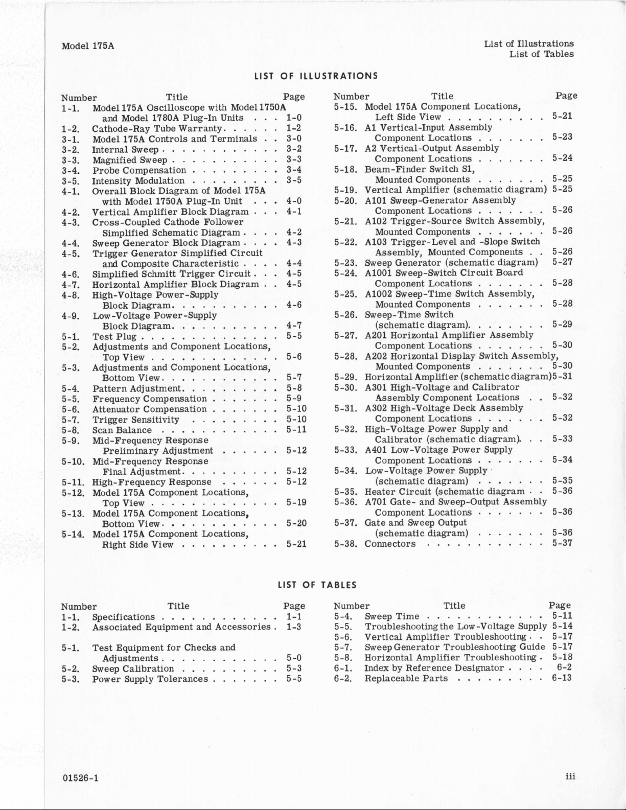
LIST
OF
ILLUSTRATIONS
List of Illustrations
List of Tables
Number Title
1-1.
1-2.
3-1.
3-2.
3-3.
3-4.
3-5.
4-1.
4-2.
4-3.
4-4.
4-5.
4-6.
4-7.
4-8.
4-9.
5-1.
5-2.
5-3.
5-4.
5-5.
5-6.
5-7.
5-8.
5-9.
5-10.
5-11.
5-12.
5-13. ModLl 175A Component Locations,
5-14. Model 175A Component Locations,
Model 175A Oscilloscope with MOI !11750A
and Model 1780A Plug-In
Cathode-Ray TubeWarranty.
Model 175A Controls and Terminals
Internal Sweep
Magnified Sweep
Probe Compensation
Intensity Modulation
Overall Block Diagram of Model 175A
with Model 1750A Plug-In
Vertical Amplifier Block Diagram
Cross-Coupled Cathode Follower
Simplified Schematic Diagram
Sweep Generator Block Diagram.
Trigger Generator Simplified Circuit
and Composite Characteristic
Simplified Schmitt Trigger Circuit.
Horizontal Amplifier Block Diagram
High-Voltage Power -Supply
Block Diagram.
Low-Voltage Power-Supply
Block Diagram.
Test Plug
Adjustments and Component Locations,
Top View
Adjustments and Component Locations,
Bottom View.
Pattern Adjustment.
Frequency Compensation
Attenuator Compensation
Trigger Sensitivity
Scan Balance
Mid
-
Frequency Response
Preliminary Adjustment
Mid-Frequency Response
Final Adjustment.
High-FrequencyResponse
Model 175A Component Locations,
T~D View
Bottom View.
Right Side View
. . .
.
. . . .
.
. .
.
. .
. . . . . . . .
.
. . . . . . . . . .
.
. .
. .
.
.
. . . .
.
Units
. . . .
.
. . . .
.
. .
. .
. . . . .
Unit
. . . . . . . .
.
.
.
. . . . . .
. . . . . . .
. . . . . . . . .
. . . . . . .
. . .
. . . . . .
. . .
. . . . . . . . .
. . .
. . .
.
. . .
.
.
. . . . .
. . . .
. .
.
. . . . . .
. . . . . . .
.
.
.
. .
. .
. . .
.
.
.
.
. .
. .
.
. .
.
.
. . .
. .
.
. . .
.
. .
. .
.
.
.
.
.
. .
.
.
.
. . .
. . . .
.
.
.
.
.
.
.
.
.
.
.
.
.
1-0
1-2
3-0
3-2
3-3
3-4
3 -5
4-0
4-1
4-2
4-3
4-4
4-5
4-5
4-6
4-7
5-5
5-6
5-7
5-8
5 -9
5-10
5-10
5-11
5-12
5-12
5-12
5-19
5-20
5-21
Number Title Page
5-15. Model 175A Component Locations,
Left Side View
5-16.
A1
Vertical-Input Assembly
Component Locations
5-17. A2 Vertical-Output Assembly
5-18. Beam-Finder Switch S1,
5-19. Vertical Amplifier (schematic diagram) 5-25
5-20. A101 Sweep-Generator Assembly
5-21. A102 Trigger-Source Switch Assembly,
5-22. A103 Trigger-Level and -Slope Switch
5-23. Sweep Generator (schematic diagram) 5-27
5-24.
5-25. A1002 Sweep-Time Switch Assembly,
5-26. Sweep-Time Switch
5-27. A201 Horizontal Amplifier Assembly
5-28. A202 Horizontal Display Switch Assembly,
5-29. Horizontal Amplifier (schematic diagram)5 -31
5-30. A301 High-Voltage and Calibrator
5-31. A302 High-Voltage Deck Assembly
5-32. High-Voltage Power Supply and
5-33. A401 Low-Voltage Power Supply
5-34. Low-Voltage Power Supply.
5-35. Heater Circuit (schematic diagram
5-36. A701 Gate- and Sweep-Output Assembly
5-37.
5-38. Connectors
Component Locations
Mounted Components
Component Locations
Mounted Components
Assembly, Mounted Components
AlOOl
Sweep-Switch Circuit Board
Component Locations
Mounted Components
(schematic diagram).
Component Locations
Mounted Components
Assembly Component Locations
Component Locations
Calibrator (schematic diagram).
Component Locations
(schematic diagram)
Component Locations
Gate
and Sweep Output
(schematicdiagram)
.
.
. . . . .
. . . . . .
. .
. . . . .
. . . . . . .
.
.
.
. .
. . . . .
. , . . . . .
.
. . .
. . .
. . . . . .
. .
. . . .
. . . . .
. . .
.
. .
. . .
.
. . . .
.
. . .
. . .
. .
. . . . . .
.
. . . .
. . . .
.
. .
.
. .
.
.
. .
.
.
.
.
.
.
.
. .
. .
.
.
.
.
.
.
.
.
5-21
5-23
5-24
5
-2
5-26
5 -26
5-26
5-28
5-28
5-29
5-30
5-30
5-32
5-32
5-33
5-34
5-35
5-36
5-36
5-36
5-37
5
LIST
Number Title Page
1-1.
Specifications
1-2. Associated Equipment and Accessories. 1-3
Test Equipment for Checks and
5-1.
5-2. Sweep Calibration
5-3. Power Supply Tolerances
01526-1
Adjustments
.
. .
. . . . . . . . .
.
. . . . . . . .
.
.
.
. .
.
. .
.
. .
. . . . .
. . .
.
1-1
5-0
5-3
5-5
OF
TABLES
Number Title Page
5-4. Sweep Time
5-5. Troubleshooting the Low -Voltage Supply 5-14
5-6. Vertical Amplifier Troubleshooting.
5-7. SweepGenerator Troubleshooting Guide 5-17
5-8. Horizontal Amplifier Troubleshooting
6-1. Index by ReferenceDesignator
6-2. Replaceable Parts
. . . . . .
.
.
. . .
.
. . . . .
. . . .
. . . .
.
.
5-11
5-17
5-18
6-2
6-13
iii
Page 6
Section
Figure
I
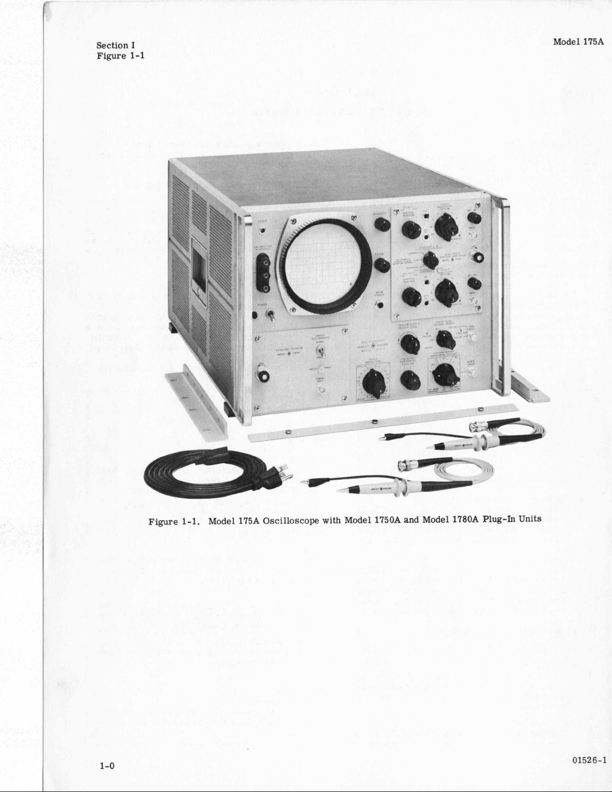
1-1
Model
175A
1-0
Figure
1-1.
Model
175A
Oscilloscope with Model
1750A
and Model
1780A
Plug-In
Units
01526-1
Page 7
Model 175A
Paragraphs
Section
1-1
to 1-8
I
SECTION
GENERAL INFORMATION
1-1.
DES
C
R
I
PTI
0
N.
1-2.
The @ Model 175A Oscilloscope
general-purpose
width
of 50 megacycles and a 6 x 10 cm display. Optional plug-in units and accessories are available to
increase the versatility of this instrument. Specifications are listed in table
1-3.
AUXILIARY EQUIPMENT.
Available associated equipment and accessories
1-4.
are
listed
in table
a. Plug-Ins.
clude dual-trace and single-trace vertical amplifiers
which collectively cover 5 mv/cm to 20 v/cm sensitivities and dc to 50-mc bandwidth. Horizontal units
include single sweep, sweep delay, a time-mark
generator, and a display scanner.
test
instrument with a vertical band-
1-1.
1-2.
Plug-in units for the Model 175A in-
is
a calibrated
Table
1-1.
I
b.
Accessories. Each oscilloscope
two Model 10003A (AC-21M) high-impedance probes
and a detachable power cable.
1-5. INSTRUMENT IDENTIFICATION.
1-6. Hewlett-Packard uses
serial number
of the serial number on your instrument
with those
sheets supplied with the manual will define differences
between your instrument andthe Model 175A described
in this manual.
1-7. WARRANTY.
1-8. Both the cathode-ray tube
carry Hewlett-Packard warranties. The
is
illustrated in figure 1-2, and a copy
the back of this manual for your use in
tube failure within the warranty period. The Model
175A warranty
Specifications
(000-00000).
on the
title
is
also at the back of this manual.
a
two-section eight-digit
If
page of this manual, change
is
supplied with
the
first
do
(crt)
and Model 175A
crt
is
three digits
the
not agree
warranty
included at
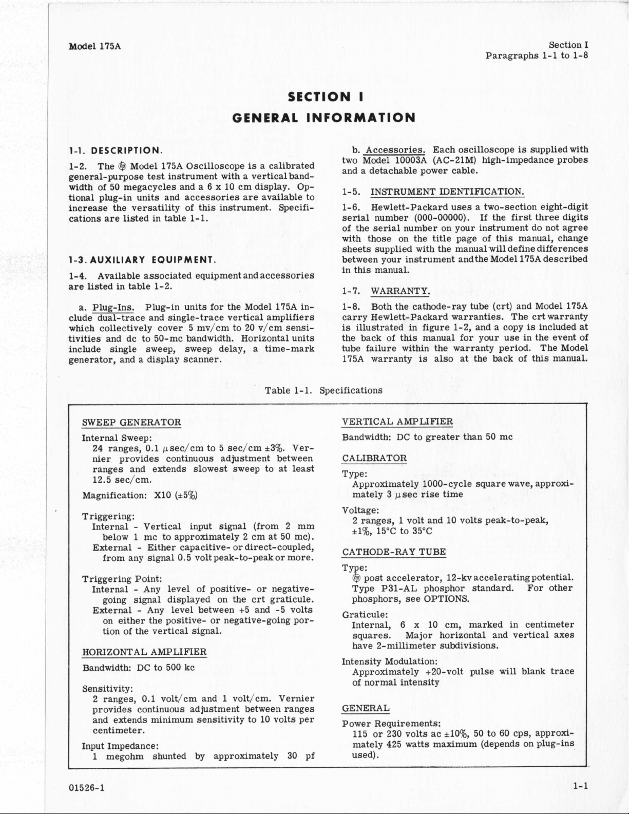
event of
SWEEP GENERATOR
Internal Sweep:
24 ranges, 0.1 psec/cm to 5 sec/cm
nier
provides continuous adjustment between
ranges and extends slowest sweep to at least
12.5 sec/cm.
Magnification: X10 (*5%)
Triggering:
Internal
below
External
from any signal 0.5 volt peak-to-peakor more.
Triggering Point:
Internal
going signal displayed on the crt graticule.
External
on either the positive- or negative-going portion of the vertical signal.
HORIZONTAL
Bandwidth DC to 500 kc
Sensitivity:
2
ranges, 0.1 volt/cm and 1 volt/cm. Vernier
provides continuous adjustment between ranges
and extends minimum sensitivity to 10 volts per
centimeter.
Input Impedance:
1
-
Vertical input signal (from 2 mm
1
mc to approximately 2 cm
-
Either capacitive-
-
Any level of positive- or negative-
-
Any level between +5 and -5 volts
AMP
LIFTER
megohm shunted by approximately 30 pf
or
*3%.
at
50 mc).
direct-coupled,
Ver-
VERTICAL AMPLIFTER
Bandwidth: DC to greater than 50 mc
CALIBRATOR
Type:
Approximately 1000-cycle square wave, approximately 3 psec rise time
Voltage:
2
ranges, 1 volt and 10 volts peak-to-peak,
*l%,
15°C to 35°C
CATHODE-RAY TUBE
Type:
@
post accelerator, 12-kv accelerating potential.
Type P31-AL phosphor standard. For other
phosphors,
Graticule:
Internal, 6 x 10 cm, marked in centimeter
squares. Major horizontal and vertical axes
have 2-millimeter subdivisions.
Intensity Modulation:
Approximately +20-volt pulse
of normal intensity
GENERAL
Power Requirements:
115 or 230 volts ac
mately 425 watts maximum (depends on plug-ins
used).
see
OPTIONS.
will
*lo%,
50 to 60 cps, approxi-
blank trace
01526-1
1-1
Page 8
Section
Figure
I
1-2
Model 175A
Table
1-1.
GENERAL (cont'd)
Dimensions:
16-3/4 inches wide, 12-1/4 inches high, 24-3/8
inches deep overall; hardware furnished for quick
conversion to 12-1/4-inch
x
19-inch rack mount,
22 inches deep behind panel.
Weight:
Net
approximately
70
lb
maximum (depends on
plug-ins used)
Plug-In Vertical Amplifiers:
($3
Model 1750A Dual Trace Vertical Amplifier,
40
dc to
@
Model 1751A Single Channel Vertical Ampli-
arx
fier,dc to 50 mc
@
Model 1752A High Gain Vertical Amplifier,
dc to 18 mc
@
Model 1753A Single Channel Vertical Amplifier, dc to 40 mc
Specifications (Cont'd)
Plug-In Horizontal Time Base Units:
($3
Model 1780A Auxiliary Unit
@
Model 1781A Sweep Delay Unit
@
Model 1782A Display Scanner
@
Model 1783A Time-Mark Generator
Accessories Furnished;
Two probes, 10003A (AC-21M),
division, one power cable
Accessories Available:
($3
1075A, 1075B (AC-83A) Viewing Hood
($3
Model 1115A Testmobile
($4
Model
ultraviolet light source for illuminating the
graticule and pre-sensitizing film
OPTIONS
02. Supplied with
07.
Supplied with
11.
Supplied with
08. Sawtooth Output (approximately -2.5 volts to
+2.5 volts) and Gate Output (+5-volt pulse
nominal, riding on a
1O:l
voltage
196B Oscilloscope Camera, includes
P2
phosphor
P7
phosphor
P11
phosphor
-
2.5 volt level).
HEWLETT-PACKARD CO. PAGE MILL
1-2
ROAD.
PAL0 ALTO. CALIF.
U.S.A.
Figure 1-2. Cathode-Ray Tube Warranty
01526-1
Page 9
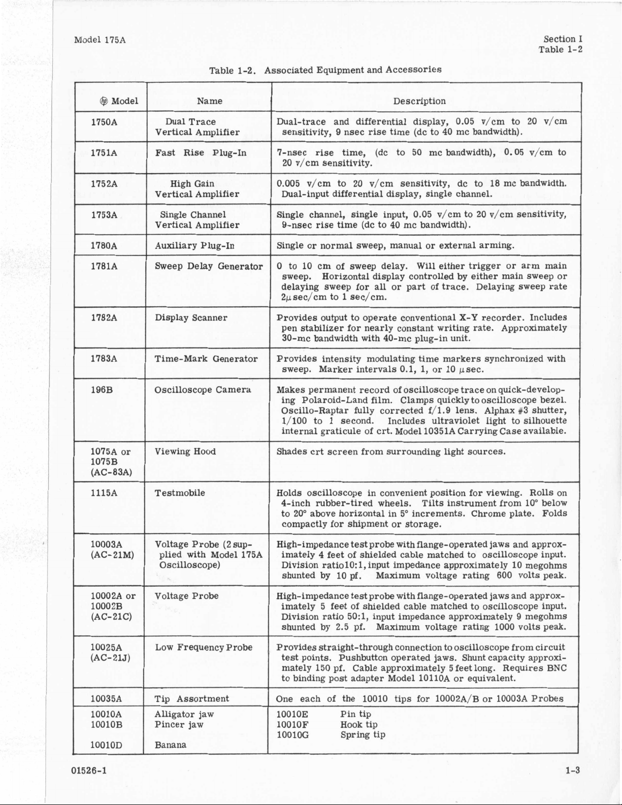
Model 175A Section I
Table
1-2
Table 1-2. Associated Equipment and Accessories
@
Model Name
Description
1750A
Dual Trace
Vertical Amplifier
1751A
1752A
Fast
High Gain
Rise Plug-In
Vertical Amplifier
1753A
Single Channel
Vertical Amplifier
1780A
1781A
Auxiliary Plug-In
Sweep Delay Generator
1782A Display Scanner
1783A
Time-Mark Generator Provides intensity modulating time markers synchronized with
Oscilloscope Camera Makes permanent record of oscilloscope trace on quick-develop-
~~ ~
1075A or
Viewing Hood
1075B
(AC-83A)
Dual-trace and differential display, 0.05 v/cm to 20 V/Cm
sensitivity, 9 nsec rise time (dc to
40
mc bandwidth).
7-nsec rise time, (dc to 50 mc bandwidth), 0.05 v/cm to
20 v/cm sensitivity.
0.005 v/cm to 20 v/cm sensitivity, dc to 18 mc bandwidth.
Dual-input differential display, single channel.
Single channel, single input, 0.05 v/cm to 20 v/cm sensitivity,
rise
9-nsec
time (dc to 40 mc bandwidth).
Single or normal sweep, manual or external arming.
to 10 cm of sweep delay.
0
Will
either trigger or arm main
sweep. Horizontal display controlled by either main sweep or
delaying sweep for all or part of trace. Delaying sweep rate
2psec/cm to
Provides output to operate conventional
1
sec/cm.
X-Y
recorder. Includes
pen stabilizer for nearly constant writing rate. Approximately
30-mc bandwidth with 40-mc plug-in unit.
1,
sweep. Marker intervals 0.1,
or 10 psec.
ing Polaroid-Land film. Clamps quickly to oscilloscope bezel.
Oscillo-Raptar fully corrected f/1.9 lens. Alphax #3 shutter,
1/100 to
internal graticule of
1
second. Includes ultraviolet light to silhouette
crt.
Model 10351A Carrying Case available.
Shades crt screen from surrounding light sources.
1115A
Testmobile Holds oscilloscope in convenient position for viewing. Rolls on
4-inch rubber-tired wheels. Tilts instrument from 10" below
to 20" above horizontal in 5" increments. Chrome plate. Folds
compactly for shipment or storage.
10003A
(AC- 21M)
10002B
(AC- 21C)
Voltage Probe (2 sup-
plied with Model 175A
Oscilloscope)
Voltage Probe 10002A or
High-impedance
imately
4
Division ratiolO:l, input impedance approximately 10 megohms
shunted
High-impedance
imately 5
Division ratio 50:
test
probe with flange-operated jaws and approx-
feet of shielded cable matched to oscilloscope input.
by
10
pf.
Maximum voltage rating 600 volts peak.
test
probe with flange-operated jaws and approx-
feet
of shielded cable matched to oscilloscope input.
1,
input impedance approximately 9 megohms
~~ ~
shunted by 2.5 pf. Maximum voltage rating 1000 volts peak.
10025A
(AC-21J)
10035A
lOOlOA
lOOlOB
lOOlOD
Low Frequency Probe
~~~~
Tip Assortment
Alligator jaw
Pincer jaw
Banana
Provides straight-through connection to oscilloscope from circuit
test
points. Pushbutton operated jaws. Shunt capacity approxi-
mately 150 pf. Cable approximately
to binding post adapter Model
5
lOllOA
feet long. Requires BNC
or equivalent.
One each of the 10010 tips for 10002A/B or 10003A Probes
lOOlOE Pin tip
lOOlOF
lOOlOG
Hook tip
Spring tip
01526-1 1-3
Page 10
Section I
Paragraphs 1-9 to 1-14
Model 175A
1-9.
SPECIAL FEATURES.
1-10. Special features of the Model 175A include the
Hewlett-Packard internal-graticule crt, PRESET
triggering, BEAM FINDER, and a cabinet which
serves both bench- and rack-mount requirements.
Optional plug-in units are provided for both the vertical and the time axis. The main vertical amplifier
rise
time
is
less
than 7 nanoseconds which provides
maximum versatility for present and future plug-ins.
1-11.
CATHODE-RAY TUBE.
1-12. The
12-kv post-accelerator type with the
cule which eliminates parallax, and an aluminized
crt
used in the Model 175A
is
a multi-grid
@
internal grati-
phosphor. The gun structure provides a large
10 cm distortionless viewing area as well as extremely high deflection-plate sensitivity. No frontpanel astigmatism control
1-13. SPECIAL CONTROLS.
1-14. Special panel controls make the Model 175A easy
to operate. With SWEEP MODE in PRESET, the
sweep will synchronize internally on nearly all signals.
BEAM FINDER enables the operator to locate the
beam when
increases the maximum sweep rate to 10 nsec/cm,
calibrated in
it
is
off screen. SWEEP MAGNIFIER
all
positions.
is
required.
6
x
1-4
01526-1
Page 11
Model
175A
Paragraphs
Section
2-1
to 2-18
11
SECTION
INSTALLATION
2-1.
INCOMING
2-2. MECHANICAL INSPECTION.
2-3. Upon receipt of your Model 175A, check the
contents of the shipment against the packing
inspect the instrument for any obvious damage received in transit. See warranty sheet at the back of
this
manual. Keep the packing material until per-
formance check
2-4. PERFORMANCE CHECK.
2-5. Check the performance of the Model 175A by
making the
manual. Use this check to verify
cations and also
inspection. Instructions for the plug-in units will be
found in the individual manuals for these instruments.
2-6. INSTALLATION.
2-7. The Model 175A
lett-Packard cabinet, suitable for bench or rack
mount. Top and bottom covers may
easy accessibility to internal parts and adjustments.
2-8. RACK MOUNTING.
2-9. Parts necessary for rack mounting are pack-
aged with
a. Remove
b. Remove
c.
Remove adhesive-backed trim strip from sides.
d. Attach filler strip along bottom edge of front
panel.
e.
Attach mounting flanges to sides with larger
notch toward bottom of instrument.
f.
Mount in standard 19-inch rack (mounting screws
not supplied).
Rear support must be supplied to the rack-.<
mounted instrument
to mechanical vibrations.
2-10.
2-11. The air filter in this instrument must receive
an oil coat before the instrument
use
to prevent excessive dirt from entering instrument
case. Recommended
No.
3
“Handi-Koter” sprayer cans at most heating-supply
stores or through your Hewlett-Packard field sales
engineer.
the
COOLING.
Filter Coat. This adhesive
INSPECTION.
has
been successfully completed.
tests
outlined in paragraph 5-5 of this
all
listed specifi-
as
part of an incoming quality-control
is
packaged in the new Hew-
be
removed for
instrument. Proceed as follows:
tilt
stand.
feet
(press foot-release button).
Note
if
it
is
to be subjected
is
placed in normal
is
Research Products Company
is
available in
list
and
II
2-12. The cooling fan and air filter are located at
the rear of the Model 175A. Leaveat least two inches
of clearance behind the instrument for the free move-
ment of air. In rack installations be sure that the
recirculation of warm
not result in high ambient temperature. Inspect the
air
filter periodically and clean
pears to be reducing the flow of cooling
section V for cleaning instructions.
2-13. POWER REQUIREMENT.
2-14. The Model 175A operates on 115 or 230 volts
*lo%,
the plug-ins used, but will not exceed approximately
425 watts. Before connecting the instrument to the
power source, be sure
rear
proper fuse
2-15. SAFETY POWER CABLE.
2-16. To protect operating personnel the National
Electrical Manufacturers’ Association (NEMA) recommends that the instrument panel and cabinet be
grounded. This instrument
conductor power cable which grounds the instrument
when plugged into an appropriate outlet. The offset
round pin on the power-cable three-prong connector
is
when operating the instrument from a two-contact
outlet, use a three-prong to two-prong adapter and
connect the green pigtail on the adapter to ground.
2-17.
2-18. To repack the Model 175A for shipment, always
use the best packaging methods available. If the
original container with
is
sales office for packing materials or instructions.
The following steps are a general guide:
the instrument.
ment”.
50
to
60
panel
Connecting to a 230-volt source with the
switch in the 115-volt position can result in
damage to the instrument.
the ground pin. To preserve the protection feature
not on hand, consult your nearest Hewlett-Packard
a. Wrap the instrument in heavy paper.
b.
Protect the panel with cardboard strips.
c.
Use a strong cardboard or wooden
d. Use ample packing material around all sides of
e.
Seal with heavy tape or metal bands.
f.
Mark the container “Fragile - Delicate Instru-
is
in the correct position, and that the
is
installed (see section VI).
REPACKAGING FOR SHIPMENT.
air
within the rack cabinet does
it
as soon as
cps. Power required dependsupon
that
the 115-230 switch on the
CAUTION
is
equipped with a three-
its
packing pads and fillers
air.
it
apSee
box.
01526-1
2-
1
Page 12
Section
Figure
111
3-1
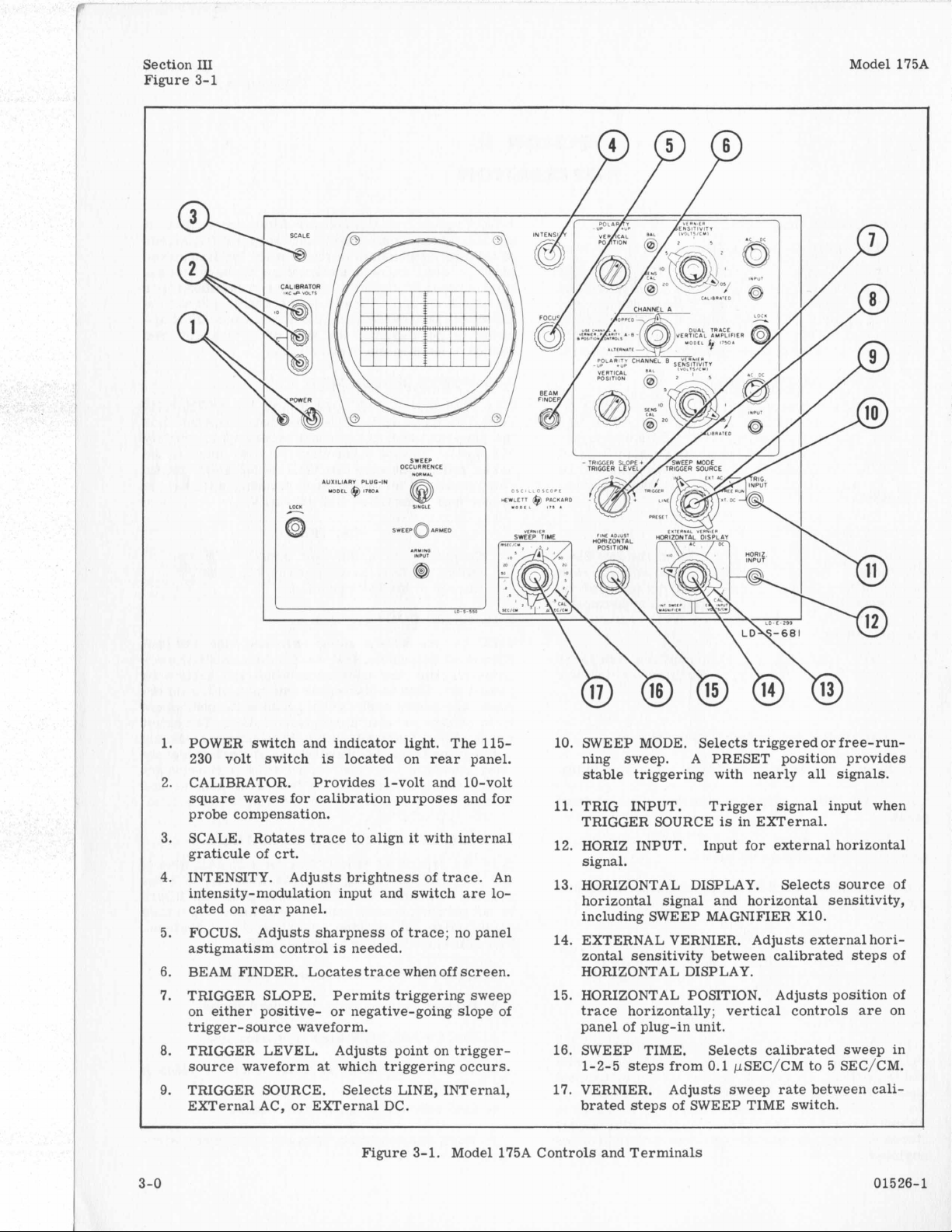
SWEEP
OCCURRENCE
Model 175A
POWER switch and indicator light. The 115-
1.
230 volt switch
CALIBRATOR. Provides 1-volt and 10-volt
2.
is
located on
rear
square waves for calibration purposes and for
probe compensation.
SCALE. Rotates
3.
graticule of
4.
INTENSITY. Adjusts brightness of
crt.
trace
to align
it
with internal
trace.
intensity-modulation input and switch
cated on
5.
FOCUS. Adjusts sharpness of trace; no panel
astigmatism control
BEAM FINDER. Locates
6.
TRIGGER SLOPE. Permits triggering sweep
7.
rear
panel.
is
needed.
trace
when off screen.
on either positive- or negative-going slope of
trigger-source waveform.
TRIGGER LEVEL. Adjusts point on trigger-
8.
source waveform
TRIGGER SOURCE. Selects LINE, INTernal,
9.
at
which triggering occurs.
EXTernal AC, or EXTernal DC.
Figure
3-1.
panel.
An
are
lo-
Model 175A Controls and Terminals
10. SWEEP MODE. Selects triggered or free-running sweep.
stable
11.
TRIG INPUT. Trigger signal input when
triggering with nearly
TRIGGER SOURCE
A
PRESET position provides
all
signals.
is
in EXTernal.
12. HORIZ INPUT. Input for external horizontal
signal.
13.
HORIZONTAL DISPLAY. Selects source of
horizontal signal and horizontal sensitivity,
including SWEEP MAGNIFIER X10.
14. EXTERNAL VERNIER. Adjusts external hori-
zontal sensitivity between calibrated steps of
HORIZONTAL DISPLAY.
15. HORIZONTAL POSITION. Adjusts position of
trace
horizontally; vertical controls
are
on
panel of plug-in unit.
16. SWEEP TIME. Selects calibrated sweep in
1-2-5 steps from 0.1 pSEC/CM to 5 SEC/CM.
17. VERNIER. Adjusts sweep
rate
between
cali-
brated steps of SWEEP TIME switch.
3-0 01526-1
Page 13
Section
Paragraphs 3-1 to 3-28
111
Model 175A
SECTION
OPERATION
3-1. GENERAL.
3-2. The front panel labeling of the Model 175A
closely describes the function of each control. The
instrument
and compatible test probes are provided. Vertical
controls are on the panel of the vertical plug-in unit.
Their operation
instrument.
3-3. BEAM FINDER.
3-4. BEAM FINDER locates the trace when
otherwise be off the screen. Depressing this button
brings the trace on the screen, defocused and intensified. The POSITION controls can then be adjusted to
bring the trace to the center of the screen.
3-5. CALIBRATION.
3-6. The CALIBRATOR amplitude
1%
from 15°C to 35°C (50°F to 95°F). Square-wave
outputs are provided at an amplitude of
and a frequency of approximately
3-7. TRIGGERING.
3-8. Four front-panel controls affect the start of the
normal sweep. They are the TRIGGER SOURCE
switch, TRIGGER LEVEL control, TRIGGER SLOPE
switch, and SWEEP MODE control.
3-9. TRIGGER SOURCE.
3-10. The TRIGGER SOURCE switch selects the
source of the sweep trigger: the power line (LINE),
the signal applied to the vertical amplifier (INT), or
an external signal applied to TRIG INPUT (EXT AC
or EXT DC). With INT
lected, the trigger signal
generator. With EX” DC selected, the trigger signal
is
3-
11.
3-12. The TRIGGER LEVEL control selects the voltage level on the trigger signal at which the sweep
starts. The control provides continuous adjustment
of the trigger level from about -5 volts to about +5
volts on external trigger signals and over a range
equivalent to
internal trigger signals.
3-13. TRIGGER SLOPE.
3-14. TRIGGER SLOPE determines whether the sweep
starts
of the trigger signal.
3-15. SWEEP MODE.
3-16. The SWEEP MODE control determines whether
the sweep requires a trigger or free runs. The control
is
has
a rise time of less than 7 nanoseconds,
is
described in the manual for that
it
might
is
accurate to
1
and 10 volts
1
kc.
or EXT AC triggering se-
is
ac-coupled to the sweep
dc-coupled to the sweep generator.
TRIGGER LEVEL.
6
centimeters of vertical deflection on
on the positive-slope or negative-slope portion
continuously adjustable with a switched position
111
(PRESET) at
PRESET triggering condition
triggered functions.
it
may be desirable to move the control out of PRE-
SET.
3-17. SWEEP CONTROLS,
3-18. SWEEP TIME.
3-19. There are 24 positions of the SWEEP TIME
control, from
to *3%. Intermediate (uncalibrated) sweep times
may be obtained by adjusting sweep time VERNIER.
3-20. SWEEP MAGNIFIER.
3-21. In the INT SWEEP
TAL DISPLAY the basic sweep time
by the setting of the SWEEP TIME switch. In the X10
magnified position the displayed sweep
faster, accurate to
scale
by
magnified signal
across; however, HORIZONTAL POSITION has enough
range to permit any portion of the presentation to be
positioned on screen.
3-22. On the fastest sweep time, 0.1 pSEC/CM X10
(10 nsec/cm) do not use the
time-scale measurements since small non-linearities
may exist. Due to the delayinthe vertical amplifier,
this portion of the trace precedes the actual triggering
point of the waveform.
trace
is
position of SWEEP TIME, the
be used.
3-23. HORIZONTAL FUNCTIONS.
3-24. HORIZONTAL DISPLAY performs three external horizontal input functions: it selects external
input, sets the sensitivity to 0.1 v/cm or
arranges the input circuit for ac or dc coupling.
3-25. INTENSITY MODULATION.
3-26. INTENSITY MODULATION controls are on the
rear panel of the Model 175A (see figure 3-5).
itive 20-volt pulse
intensities.
3-27. STEP-BY-STEP PROCEDURES.
3-28. Figure 3-1 briefly describes the function of
each of the Model 175A controls.
cedures for a few basic operations are given in figures 3-2 through 3-5. Included are instructions for
compensating the probes. The numbers on each control refer
the illustration.
its
counterclockwise extreme. The
is
best for nearly all
At
some discrete frequencies
5
SEC/CM
10 to obtain the actual sweep time. The
is
positioned off screen in the 10 pSEC/CM X10
to
the corresponding step in the text below
to
0.1
~SEC/CM,
X1
position of HORIZON-
is
*5%.
Divide the SWEEP TIME
actually 10 screen diameters
first
5 cm of trace for
As
long as the
full
10-cm display may
will
blank the trace at normal
Step-by-step pro-
accurate
that
indicated
is
10 times
first 5 cm of
1
v/cm, and
A
pos-
01526-1
3-
1
Page 14
Section
Figure 3-2
111
SWEEP
OCCURRENCE
1
1
Model
175A
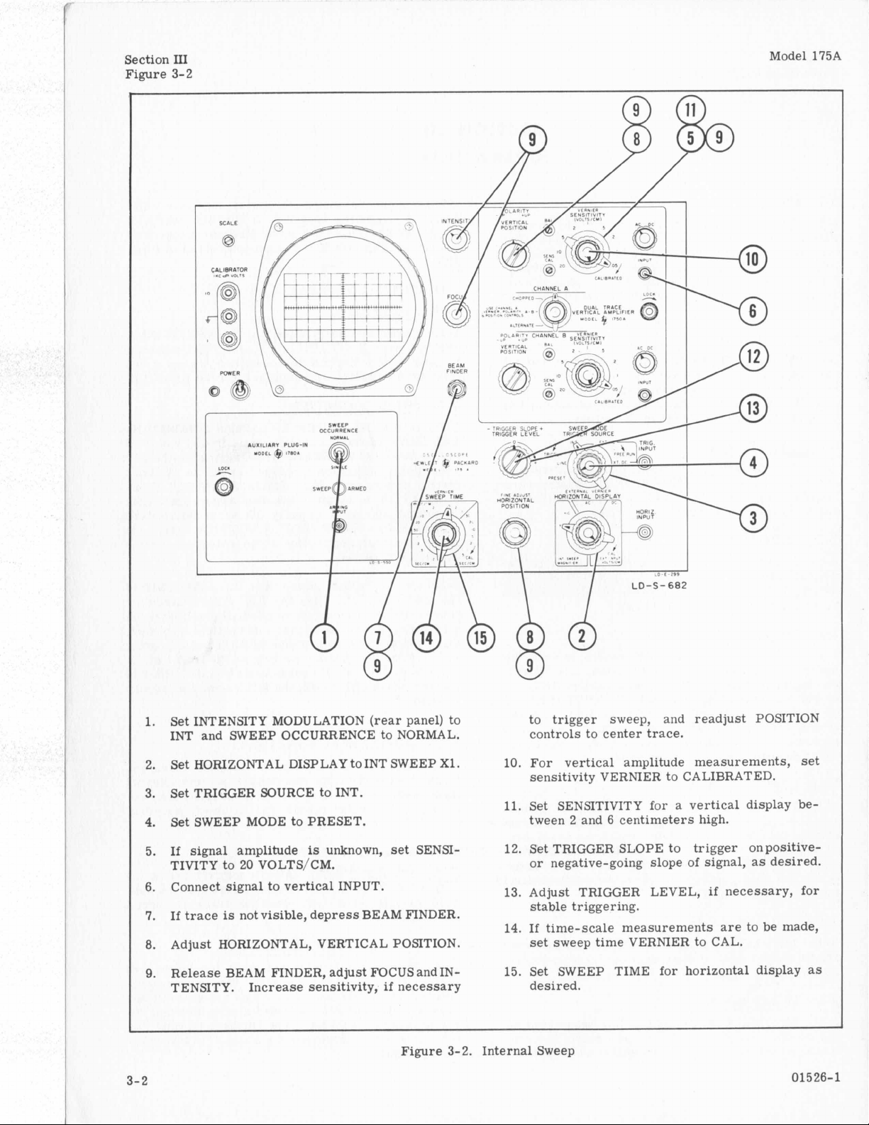
Set INTENSITY MODULATION (rear panel) to
1.
INT and SWEEP OCCURRENCE to NORMAL.
Set HORIZONTAL DISPLAY to INT SWEEP X1.
2.
Set TRIGGER SOURCE to INT.
3.
Set SWEEP MODE to PRESET.
4.
If
5.
6.
7.
8.
9.
3-2 01526-1
signal amplitude
TIVITY to 20 VOLTS/CM.
Connect signal to vertical INPUT.
If trace
Adjust HORIZONTAL, VERTICAL POSITION.
Release BEAM FINDER, adjust FOCUS and IN-
TENSITY. Increase sensitivity,
is
not visible, depress BEAM FINDER.
is
unknown,
set
SENSI-
if
necessary
Figure 3-2. Internal Sweep
to trigger sweep, and readjust POSITION
controls to center trace.
10. For vertical amplitude measurements,
sensitivity VERNIER to CALIBRATED.
11.
Set SENSITIVITY for a vertical display
tween 2 and 6 centimeters high.
12. Set TRIGGER SLOPE to trigger onpositive-
or negative-going slope of signal,
13. Adjust TRIGGER LEVEL,
stable triggering.
14. If time-scale measurements
set
sweep time VERNIER to CAL.
15. Set SWEEP TIME for horizontal display as
desired.
as
if
necessary, for
are
to be made,
set
be-
desired.
Page 15
Model
175A
INTENSITY
@
@
BEAM FlNDfR
-
TRIGGEff
TRIGGER
SLOPE
LEVEL
Section
III
Figure 3-3
__
. . . .
t
SWEEP
WE
TRIGGER
SOURCE
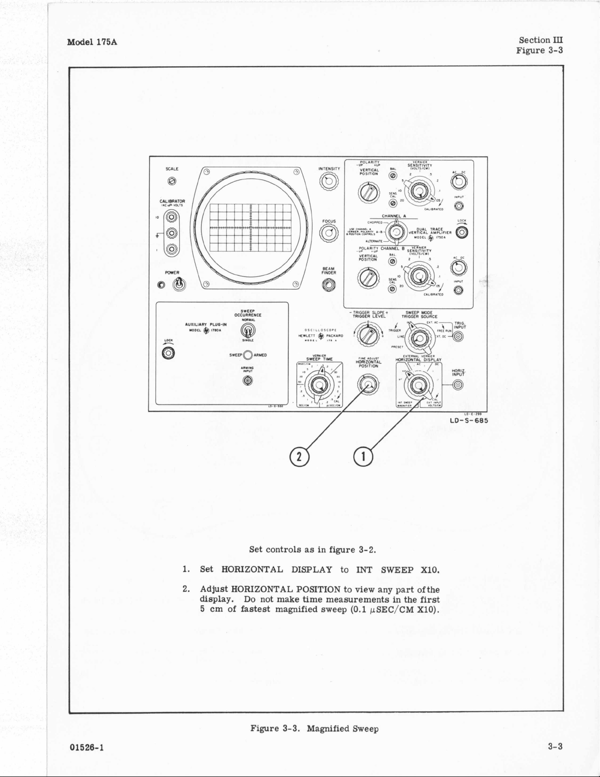
Set controls as in figure 3-2.
1. Set HORIZONTAL DISPLAY to INT
SWEEP
X10.
2. Adjust HORIZONTAL POSITION to view any part of the
display. Do
5
cm of fastest magnified sweep (0.1
not make time measurements in the first
pSEC/CM
X10).
Figure 3-3. Magnified Sweep
01526-1 3- 3
Page 16
Section
Figure
111
3-4
-
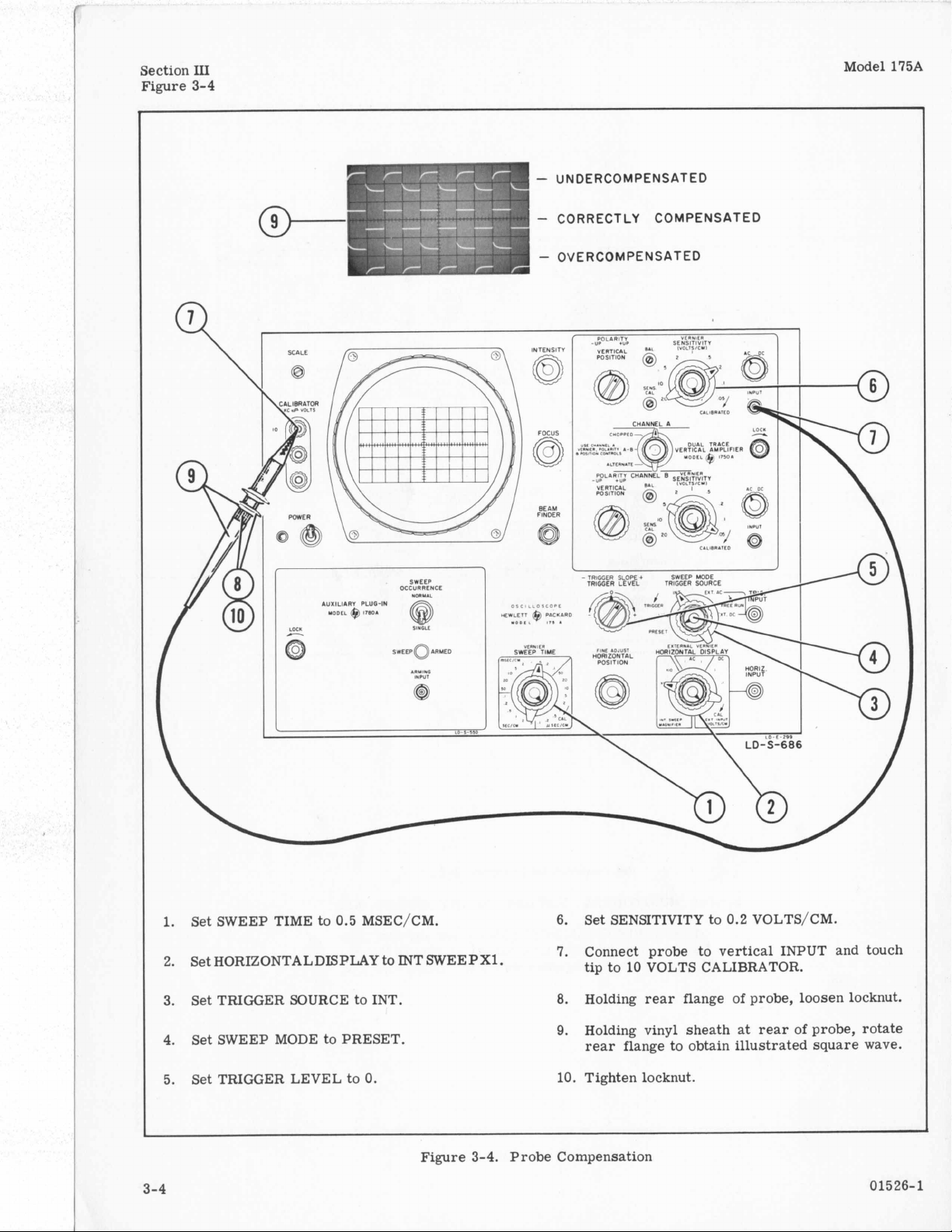
UNDERCOMPENSATED
-
CORRECTLY COMPENSATED
-
OVERCOMPENSATED
Model 175A
SWEEP
PLUG-IN
OCCURRENCE
69
IlMCLL
Connect probe to vertical INPUT and touch
7.
tip to 10 VOLTS CALIBRATOR.
8.
Holding rear flange of probe, loosen locknut.
Holding vinyl sheath
9.
at
rear of probe, rotate
rear flange to obtain illustrated square wave.
AUXILIARY
LO<.
1.
Set SWEEP TIME to 0.5 MSEC/CM. 6. Set SENSITIVITY to 0.2 VOLTS/CM.
2.
Set HORIZONTALDISPLAY to INTSWEEPXl.
3.
Set TRIGGER SOURCE to INT.
Set SWEEP MODE to PRESET.
4.
3-4
5.
Set TRIGGER LEVEL to
0.
Figure
10. Tighten locknut.
3-4.
Probe Compensation
01526-
1
Page 17
Model
175A
Section
III
Figure 3-5
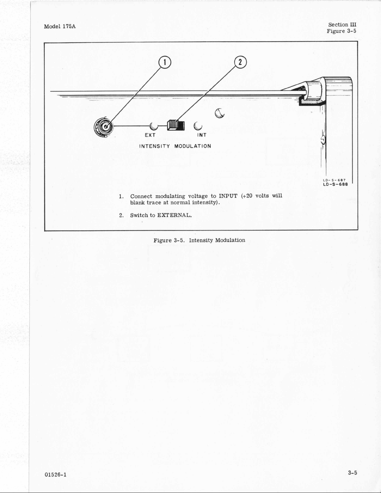
INTENSITY
Connect modulating voltage to INPUT (+20 volts will
1.
blank trace
2.
Switch to EXTERNAL.
MODULATION
at
normal intensity).
Figure 3-5. Intensity Modulation
LD-
5-
687
LD-S-688
01526-1
3-
5
Page 18
Section
Figure
IV
4-1
VERTICAL
PRESENTATION
9
\
CHANNELA
CHANNEL
B
Model
175A
I
Q
[SENSITIVITY1
I
I I
9
1-1
I
I
!Qm]
\
\
‘.C
;;I
I
,I
I
I.,
’
I
TRACE
AMPLIFIER
I
I
9
[VERTICAL
4
POSITION/
VERTICAL
AMPLIFIER
\
7--
I
ro
CRT
vmn
CA
D
Ef
PL A TES
L
L
€C
nON
-1
I
I
I
I
I
I
I
I
4-0
Figure
4-1.
Overall
Model
Block
1750A
Diagram
Plug-In
of
Unit
Model
175A
with
01526-1
Page 19
Model
175A
Section
Paragraphs 4- 1 to
4-
IV
10
SECTION
PRINCIPLES
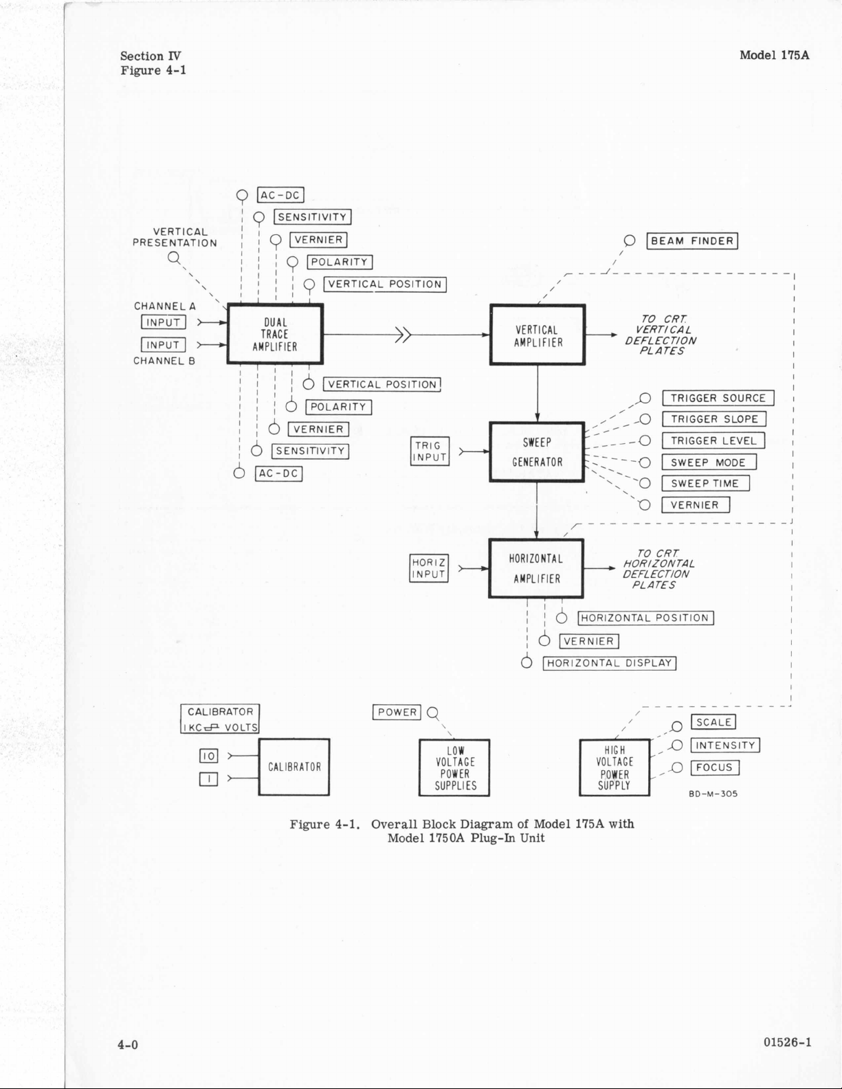
4-1.
OVERALL FUNCTIONAL DESCRIPTION.
4-2. The Model 175A consists of a high- and a lowvoltage supply, a vertical and
a
sweep generator and a calibrator. Bothpower sup-
plies are regulated,
tions include a gate- and sweep-output circuit not
included in the standard instrument. Figure 4-1
shows
the main functional units and controls.
a dual-trace plug-in amplifier has been shown as part
of the diagram. The circuits of the plug-in units are
described in the manuals for those instruments. Circuit diagrams
5-19 to 5-38.
4-3. VERTICAL AMPLIFIER. The vertical amplifier delays the signal received from the dual-trace
amplifier and applies the amplified signal to the vertical deflection plates of the crt. Before the signal
is
signal to the sweep generator for internal triggering
of the sweep.
4-4. SWEEP GENERATOR. The sweep generator
accepts a trigger signal from an internal or external
source and generates a fast-rising trigger which
synchronized with the trigger signal. The trigger
starts
the beam horizontally across the crt screen. The
sweep generator thus provides a linear time base on
which to measure the vertical signal. The sweep
generator also provides an unblanking pulse to turn
on the crt beam during the sweep.
4-5. HORIZONTAL AMPLIFIER. The horizontal
amplifier converts the internal sweep or external
a
block diagram of the instrument illustrating
delayed, the vertical amplifier applies part of the
the linearly rising sweep voltage which drives
of
the
as
Model
a
horizontal amplifier,
is
the dc heater supply. Op-
For clarity,
175A are shown in
figures
is
IV
OF
OPERATION
signal
the signal to the level required
deflection plates of the crt.
4-6. CALIBRATOR. The calibrator multivibrator
generates a square wave of about
and 10-volt outputs.
4-7. HIGH-VOLTAGE POWER SUPPLY. The highvoltage power supply
cuit which generates the three regulated dc voltages
required for operation of the crt.
4-8. LOW-VOLTAGE POWER SUPPLIES. Operating voltages for all the oscilloscope circuits, including the high-voltage supply, are provided
low-voltage power supplies.
regulated.
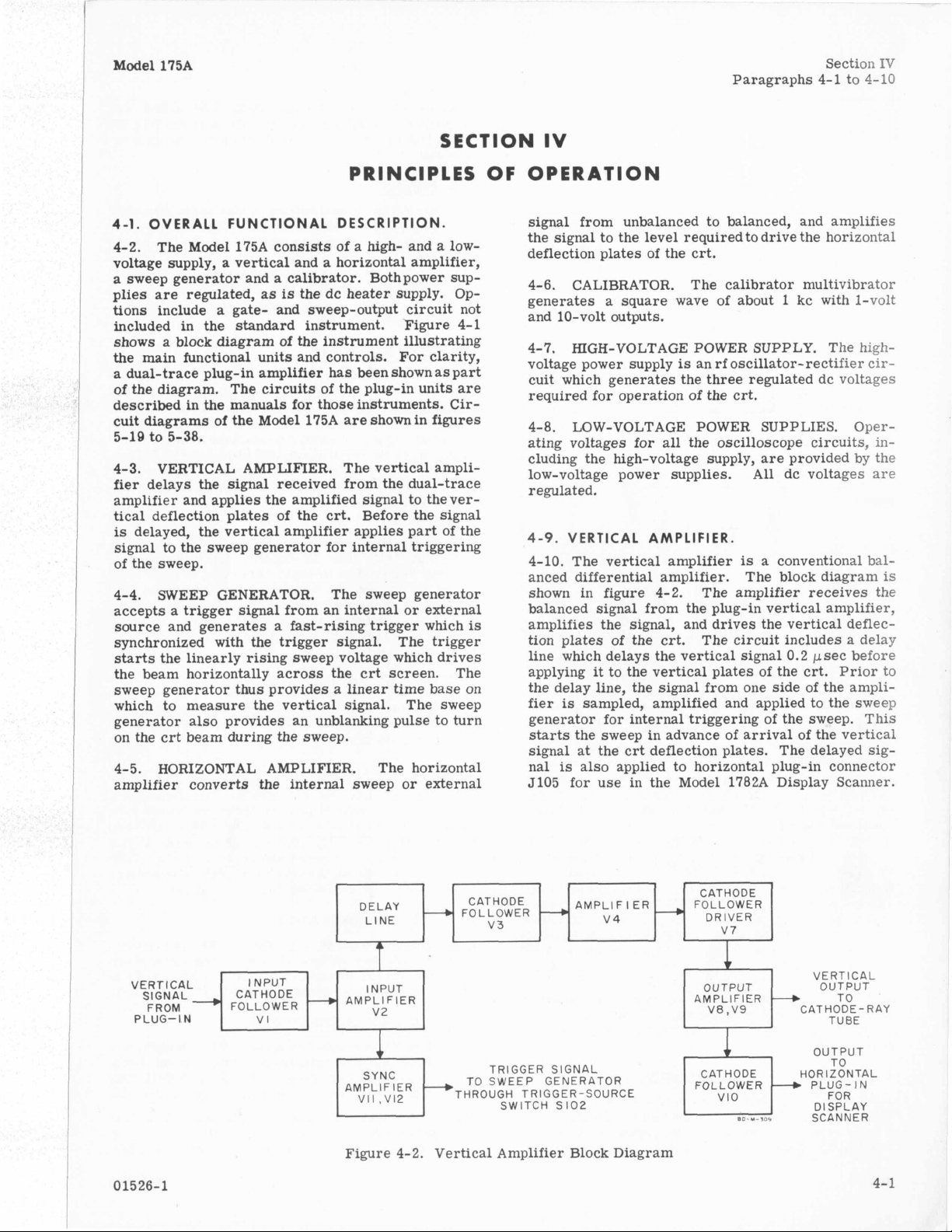
4-9.
4-10. The vertical amplifier
anced differential amplifier. The block diagram
shown in figure 4-2. The amplifier receives the
balanced signal from the plug-in vertical amplifier,
amplifies the signal, and drives the vertical deflection plates of the
line which delays the vertical signal 0.2 psec before
applying
the delay line, the signal from one side of the amplifier
generator for internal triggering of the sweep. This
starts
signal at the crt deflection plates. The delayed signal
5105 for use in the Model 1782A Display Scanner.
from unbalanced to balanced, and amplifies
to
drive the horizontal
1
kc with 1-volt
is
an
rf
oscillator-rectifier cir-
All
dc voltages are
VERTICAL AMPLIFIER.
is
a conventional bal-
crt.
The circuit includes a delay
it
to the vertical plates of the crt. Prior to
is
sampled, amplified and applied to the sweep
the sweep in advance of arrival of the vertical
is
also applied to horizontal plug-in connector
by
the
is
CATHODE
DELAY
LINE
VERTICAL INPUT
SIGNAL
FROM
PLUG-IN
01526-1 4-1
CATHODE
FOLLOWER
INPUT
AMPLIFIER
Figure 4-2. Vertical Amplifier Block Diagram
CATHODE AMPLIF I ER
-
FOLLOWER
v3
TRIGGER SIGNAL
TO SWEEP GENERATOR
THROUGH TRIGGER-SOURCE
+
A
SWITCH
SI02
v4
FOLLOWER
--*
DRIVER
v7
OUTPUT
AMPLIFIER CATHODE-RAY TO
CATHODE
FOLLOWER
-
I
CAL
VERT
OUTPUT
TUBE
DISPLAY
SCAN NE
R
Page 20
Section
IV
Paragraphs 4-11 to 4-29
Model 175A
INPUT+
---
I
V6A
U
INPUT+
t
+V
Figure 4-3. Cross-Coupled Cathode Follower
Simplified Schematic Diagram
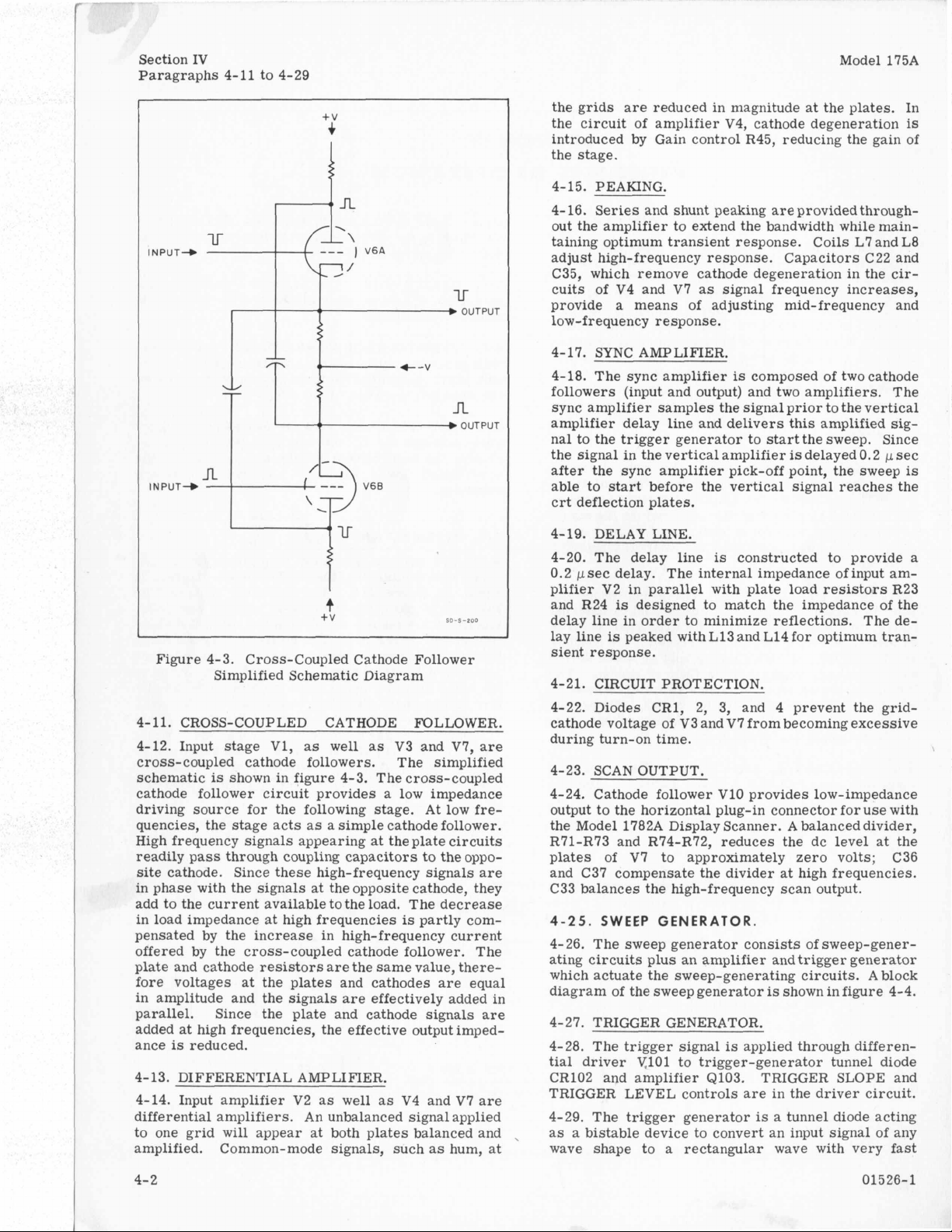
4-11. CROSS-COUPLED CATHODE FOLLOWER.
4-12. Input stage
cross-coupled cathode followers. The simplified
schematic
is
cathode follower circuit provides
driving source for the following stage.
quencies, the stage acts as
High frequency signals appearing
readily pass through coupling capacitors to the opposite cathode. Since these high-frequency signals are
in phase with the signals
add to the current available to the load. The decrease
in load impedance at high frequencies
pensated by the increase in high-frequency current
offered by the cross-coupled cathode follower.
plate and cathode resistors are the same value, there-
fore voltages
in amplitude and the signals are effectively added in
parallel. Since the plate and cathode signals are
added at high frequencies, the effective output imped-
ance
is
reduced.
4- 13. DIFFERENTIAL AMPLIFIER.
4-14. Input amplifier
differential amplifiers. An unbalanced signal applied
to one grid will appear at both plates balanced
amplified. Common-mode signals, such as hum, at
V1,
as
well
as
V3 and V7, are
shown in figure 4-3. The cross-coupled
a
low impedance
At
a
simple cathode follower.
at
the plate circuits
at
the opposite cathode, they
low fre-
is
partly com-
The
at
the plates and cathodes are equal
V2
as well
as
V4 and V7 are
and
the grids
the circuit of amplifier V4, cathode degeneration
are
reduced in magnitude at the plates.
In
is
introduced by Gain control R45, reducing the gain of
the stage.
4-15. PEAKING.
4- 16. Series and shunt peaking are provided through-
out the amplifier to extend the bandwidth while maintaining optimum transient response. Coils L7 and L8
adjust high-frequency response. Capacitors C22 and
C35, which remove cathode degeneration in the circuits of V4 and V7
provide a means of adjusting mid-frequency
as
signal frequency increases,
and
low-frequency response.
4-17. SYNC AMPLIFIER.
4-18. The sync amplifier
is
composed of two cathode
followers (input and output) and two amplifiers. The
sync amplifier samples the signal prior to the vertical
amplifier delay line and delivers this amplified signal to the trigger generator to start the sweep. Since
the signal in the vertical amplifier
is
delayed 0.2 p sec
after the sync amplifier pick-off point, the sweep is
able to
start
before the vertical signal reaches the
crt deflection plates.
4-19. DELAY LINE.
4-20. The delay line
is
constructed to provide
0.2 psec delay. The internal impedance of input amplifier
and R24
V2
in parallel with plate load resistors R23
is
designed to match the impedance of the
delay line in order to minimize reflections. The delay line
is
peaked with L13 and L14 for optimum tran-
sient response.
4-21. CIRCUIT PROTECTION.
4-22. Diodes CR1,
2,
3, and 4 prevent the gridcathode voltage of V3 and V7 from becoming excessive
during turn-on time.
4-23. SCAN OUTPUT.
4-24. Cathode follower V10 provides low-impedance
output to the horizontal plug-in connector for use with
the Model 1782A Display Scanner.
R71-R73 and R74-R72, reduces the dc level
A
balanced divider,
at
the
plates of V7 to approximately zero volts; C36
and C37 compensate the divider
at
high frequencies.
C33 balances the high-frequency scan output.
4-25.
SWEEP
GENERATOR.
4-26. The sweep generator consists of sweep-generating circuits plus an amplifier and trigger generator
which actuate the sweep-generating circuits.
diagram of the sweep generator
is
shown in figure 4-4.
A
block
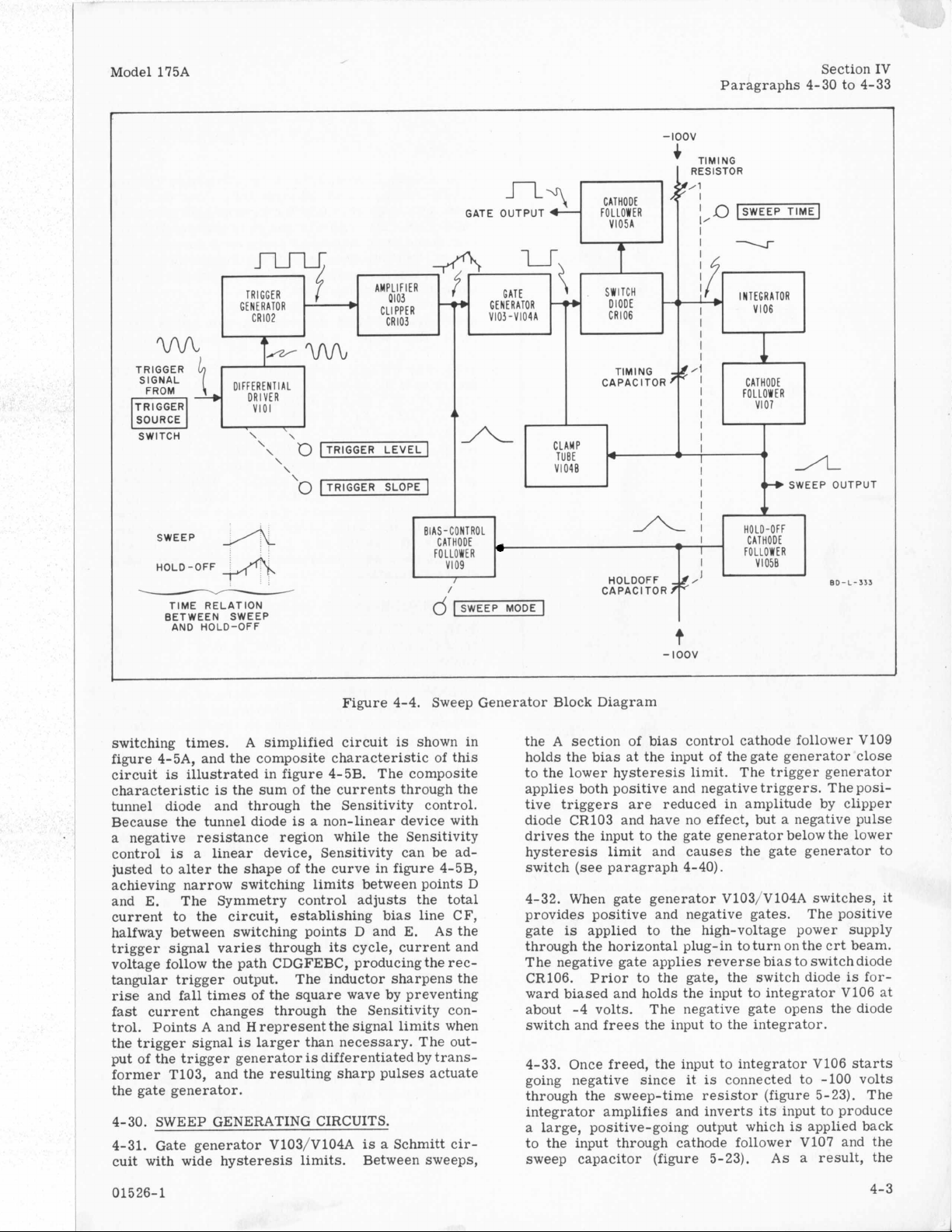
4-27. TRIGGER GENERATOR.
4-28. The trigger signal is applied through differential driver
YlOl
to trigger-generator tunnel diode
CR102 and amplifier Q103. TRIGGER SLOPE and
TRIGGER LEVEL controls are in the driver circuit.
4-29. The trigger generator
as
a
bistable device to convert
wave shape to
a
rectangular wave with very
is
a
tunnel diode acting
an
input signal of any
fast
a
4- 2
01526-1
Page 21
Model 175A
-IOOV
'
Section IV
Paragraphs 4-30 to 4-33
TIMING
SWITCH
SWEEP
HOLD-OFF
TIME RELATION
BETWEEN SWEEP
AND HOLD-OFF
A
4
nx
GATE OUTPUT
BIAS-CONTROL
CATHODE
FOLLOWER
VI09
I
/
I
SWEEP MODE
1
FOLLOW CATHODE ER
V105A
TIMING
CAPACITOR
HOLDOFF
CAPACITOR
-IOOV
I
-i?Nf
f4
I
CATHODE
I
FOLLOWER
I
I
-1
-
I
-&/I
f
VI07
4b-b
CATHODE
FOLLOWER
VI058
A
t
SWEEP OUTPUT
BO-
L-331
Figure 4-4. Sweep Generator Block Diagram
switching times. A simplified circuit
is
shown in
figure 4-5A, and the composite characteristic of this
circuit
characteristic
is
illustrated in figure 4-5B. The composite
is
the sum of the currents through the
tunnel diode and through the Sensitivity control.
Because the tunnel diode
a
negative resistance region while the Sensitivity
control
justed to
is
a linear device, Sensitivity can be ad-
alter
the shape of the curve in figure 4-5B,
is a non-linear device with
achieving narrow switching limits between points D
and E. The Symmetry control adjusts the total
current
halfway between switching points D and E.
trigger signal varies through
voltage follow the path CDGFEBC, producing the
to
the circuit, establishing bias line CF,
its
cycle, current and
As
rec-
the
tangular trigger output. The inductor sharpens the
rise and fall times of the square wave by preventing
fast
current changes through the Sensitivity con-
trol. Points A and
the trigger signal
put
of
the trigger generator
H
represent the signal limits when
is
larger than necessary. The out-
is
differentiated by transformer T103, and the resulting sharp pulses actuate
the gate generator.
4-30. SWEEP GENERATING CIRCUITS.
4-31. Gate generator V103/V104A
is
a
Schmitt
cir-
cuit with wide hysteresis limits. Between sweeps,
the A section of bias control cathode follower VI09
holds the bias at the input of thegate generator close
to the lower hysteresis limit.
The trigger generator
applies both positive and negative triggers. The positive triggers
are
reduced in amplitude by clipper
diode CR103 and have no effect, but a negative pulse
drives the input to the gate generator below the lower
hysteresis limit and causes the gate generator to
switch
4-32. When gate generator V103/V104A switches,
(see
paragraph 4-40).
it
provides positive and negative gates. The positive
gate
is
applied to the high-voltage power supply
through the horizontal plug-in to turn on the crt beam.
The negative gate applies reverse bias to switchdiode
CR106. Prior to the gate, the switch diode
is
forward biased and holds the input to integrator V106 at
about -4 volts. The negative gate opens the diode
switch and frees the input to the integrator.
4-33. Once freed, the input to integrator V106 starts
going negative since it
is
connected to
-100
volts
through the sweep-time resistor (figure 5-23). The
integrator amplifies and inverts its input to produce
a
large, positive-going output which
is
applied back
to the input through cathode follower V107 and the
sweep capacitor (figure 5-23).
As
a result, the
01526-1
4-3
Page 22

Section IV
Paragraphs
A.
CIRCUIT
I
5.5
uc?
4-34
to
0
4-41
+V
4
I
W-LI
OUTPUT
TRIGGER
SYMMETRY
Model
175A
diode
CR106.
integrator
The switch diode returns the input of
V106
to its pre-sweep level, discharging
the sweep capacitor.
4-35.
During a sweep time, hold-off cathode follower
V105B
ends, this capacitor
V103/V104A
charges a hold-off capacitor. After the sweep
lets
the input to gate generator
down slowly enough to prevent that circuit from being triggered again until the remaining
sweep circuits have recovered completely. The
SWEEP TIME switch changes the size of the hold-off
capacitor with sweep time.
4-36.
Clamp
from the same voltage level, about
4-37.
The SWEEP MODE control
determines the no-signal bias
erator
tion of bias control cathode follower
V104B
V103jV104A
ensures that each sweep starts
-50
volts.
R172
at
the input to gate gen-
by setting the
(figure
bias
on the A sec-
V109.
5-23)
With the
control set to PRESET or in the TRIGGER portion of
its adjustable range, the gate generator bias cannot
drop below its lower hysteresis limit unless the trigger generator provides a trigger. With the control
set in the FREE RUN portion of its adjustable range,
the gate bias
teresis limit. Thus
is
allowed to drop below its lower hys-
as
the hold-off capacitor
dis-
charges, it lets the gate generator bias all the way
down to the lower hysteresis limit, and another sweep
starts automatically.
-
V
LD-
Y
-
643
8.
Figure
I
COMPOSITE CURVE
4-5.
Trigger Generator Simplified Circuit
and Composite Characteristic
V106
change in voltage at the input to integrator
ing the sweep time
is
only about one volt. Voltage
dur-
across the sweep resistor, then, changes by about
1%,
and the current through the resistor changes by
the same amount. The current through the sweep
resistor
is
the charging current for the sweep capacitor; therefore, the voltage across the sweep capacitor
changes quite linearly with time, and the sweep signal
is
a nearly linear voltage ramp. The SWEEP
TIME switch changes the value of sweep resistor or
capacitor to change the sweep time. The sweep output
is
applied to the horizontal amplifier through the
horizontal plug-in.
4-34.
An
attenuated sweep signal is applied to the
input of gate generator
cathode follower
cathode follower
V105B
V109.
V103, V104A
through hold-off
and section B of bias control
This signal drives the input
of the gate generator up to the upper hysteresis limit
and causes the gate generator to switch back to its
pre-sweep state. The gate generator then ends the
the gates, blanking the crt and forward biasing switch
4-38.
SINGLE-SWEEP OPERATION,
4-39.
The SWEEP OCCURRENCE switch (on the panel
of the horizontal plug-in unit) selects normal or
single-sweep operation. Normal operation
is
discussed above. For single-sweep operation, the
SWEEP OCCURRENCE switch converts
Schmitt circuit.
cathode follower
As
the sweep signal from hold-off
V105B
rises
to end the gate from
V109
into a
the gate generator, the sweep signal also switches
the Schmitt circuit of
and
V109A
is
cut off. The B section of
holds the input to gate generator
enough
so
that triggers from the trigger generator
V109
so
that
V103/V104A
V109B
conducts
V109
then
high
cannot actuate the gate generator, and the sweep
generating circuits are effectively disabled.
itive signal applied to
circuit of
V109
so
cut off. The A section of
that
V109A
V109A
V109
switches the Schmitt
conducts and
then sets the input to
A
pos-
V109B
is
the gate generator according to the setting of the
SWEEP MODE control, and the sweep generating circuits are effectively armed. The switching signal
for
V109.4
can be an external signal applied to the
ARMING INPUT connector or an internal signal obtained by switching SWEEP MODE control out of its
PRESET position.
4-40.
SCHMITT TRIGGER CIRCUIT.
4-41.
The Schmitt trigger circuit
is
a form of bistable multivibrator used where fast-rising signals
are required. Figure
4-6
shows a simplified Schmitt
trigger circuit and input and output waveforms. If
initially the input voltage is such that
V2
conducts.
itive, it
As
the input voltage becomes more
will
eventually reach a predetermined level
(a) at which the circuit changes state;
V1
V1
is
cut off,
pos-
conducts
4- 4
01526-
1
Page 23
Mxlel
175A
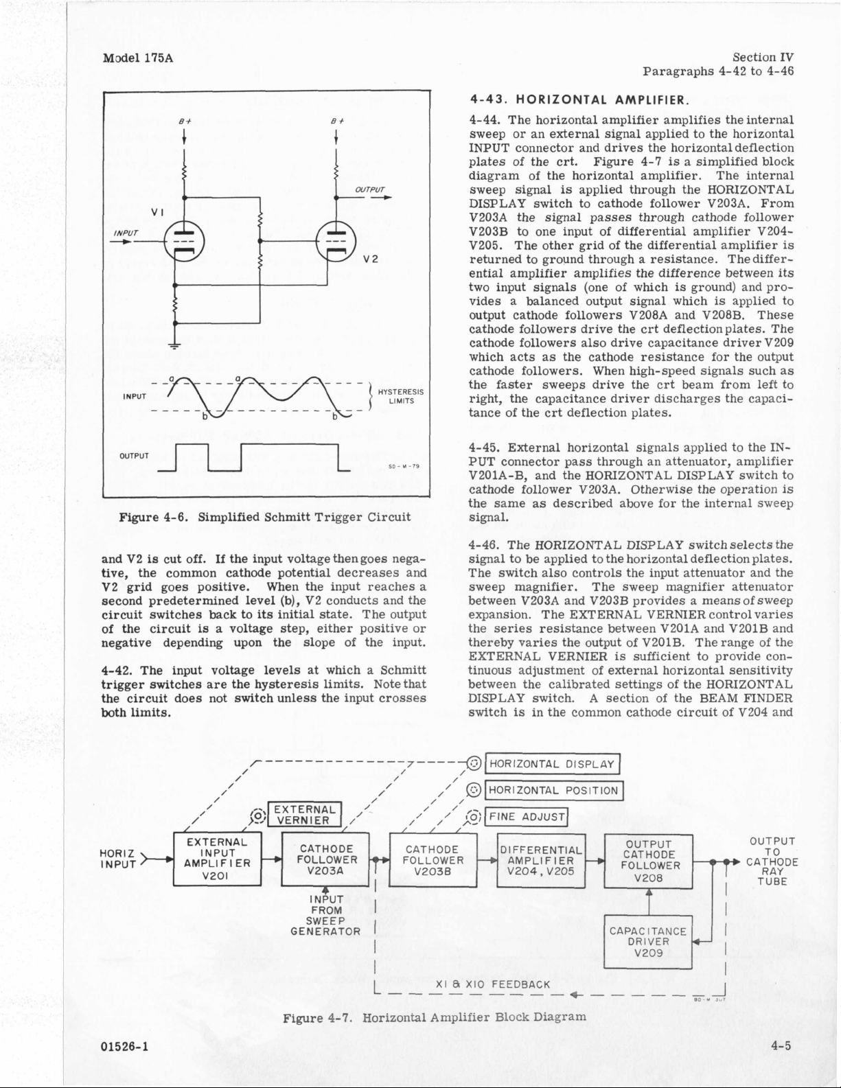
Section
Paragraphs 4-42 to 4-46
IV
E+
c
VI
I
INPUT
-9
P--
OUTPUT
Figure
4-6.
Simplified Schmitt Trigger Circuit
Et
+
SD-u-79
4-43.
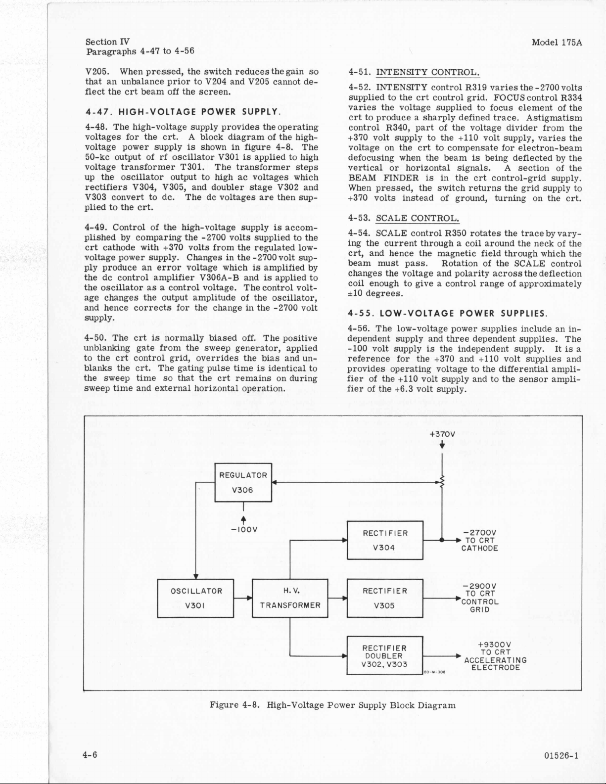
4-44. The horizontal amplifier amplifies the internal
sweep or an external signal applied to the horizontal
INPUT connector and drives the horizontal deflection
plates of the crt. Figure
diagram of the horizontal amplifier. The internal
sweep signal
DISPLAY switch to cathode follower V203A. From
V203A the signal passes through cathode follower
V203B to one input of differential amplifier V204V205. The other grid of the differential amplifier
returned to ground through a resistance. The differential amplifier amplifies the difference between its
two input signals (one of which
vides
output cathode followers V208A and V208B. These
cathode followers drive the crt deflection plates. The
cathode followers also drive capacitance driver V209
which acts
cathode followers. When high-speed signals such
the faster sweeps drive the crt beam from
right, the capacitance driver discharges the capacitance of the crt deflection plates.
4-45.
PUT connector pass through an attenuator, amplifier
V201A-B, and the HORIZONTAL DISPLAY switch to
cathode follower V203A. Otherwise the operation
the same
signal.
HORIZONTAL
is
a
balanced output signal which
as
the cathode resistance for the output
External horizontal signals applied to the
as
described above for the internal sweep
AMPLIFIER.
4-7
is
a
simplified block
applied through the HORIZONTAL
is
ground) and pro-
is
applied to
left
is
as
to
IN-
is
and V2
tive, the common cathode potential decreases and
V2 grid goes positive. When the input reaches
second predetermined level
circuit
of the circuit
negative depending upon the slope of the input.
4-42.
trigger switches are the hysteresis limits. Note that
the circuit does not switch unless the input crosses
both limits.
HORIZ
INPUT
is
cut off.
switches back to
The input voltage levels
*
If
the input voltagethengoes nega-
(b),
its
initial state.
is a voltage step, either positive or
EXTERNAL
INPUT
AMPLl
v201
F I ER
-+
GENERATOR
V2
conducts and the
at
which a Schmitt
C
ATH 0 DE
FOLLOWER
V203A
4
INPUT
FROM
SWEEP
The output
CATHODE DIFFERENTIAL
FOLLOWER
V203B
1
1
I
4-46. The HORIZONTAL DISPLAY switch selects the
signal to be applied to the horizontal deflection plates.
The switch also controls the input attenuator and the
a
sweep magnifier. The sweep magnifier attenuator
between V203A and V203B provides
expansion. The EXTERNAL VERNIER control varies
the series resistance between V201A and V201B and
thereby varies the output of V201B. The range of the
EXTERNAL VERNIER
tinuous adjustment of external horizontal sensitivity
between the calibrated settings of the HORIZONTAL
DISPLAY switch.
switch
-+
AMPLIFIER
V204,
is
in the common cathode circuit of V204 and
V205
is
sufficient to provide con-
A
section of the BEAM FINDER
OUTPUT OUTPUT
CATHODE
-+
FOLLOWER RAY
V208 TUBE
T
CAPACITANCE
DRIVER
V209
a
means of sweep
CATHODE
I
I
t
I
TO
01526-1
Figure 4-7. Horizontal Amplifier Block Diagram
4-5
Page 24
Section
W
Paragraphs 4-47 to 4-56
Model 175A
V205. When pressed, the switch reduces the gain
so
that an unbalance prior to V204 and V205 cannot de-
flect the crt beam off the screen.
4-47.
HIGH-VOLTAGE POWER SUPPLY.
4-48. The high-voltage supply provides the operating
voltages for the crt.
voltage power supply
50-kc output
of
voltage transformer T301.
up the oscillator output to high
A
block diagram of the high-
is
shown in figure 4-8. The
rf
oscillator V301
is
applied to high
The transformer steps
ac
voltages which
rectifiers V304, V305, and doubler stage V302 and
V303 convert to dc.
The dc voltages
are
then sup-
plied to the crt.
4-49. Control of the high-voltage supply
is
accom-
plished by comparing the -2700 volts supplied to the
crt cathode with +370 volts from the regulated lowvoltage power supply.
ply produce an error voltage which
the dc control amplifier V306A-B and
the oscillator
as
Changes in the -2700 volt sup-
is
amplified by
is
applied to
a
control voltage. The control voltage changes the output amplitude of the oscillator,
and hence corrects for the change in the -2700 volt
supply.
4-50. The crt
unblanking
is
normally biased off. The positive
gate from the sweep generator, applied
to the crt control grid, overrides the bias andun-
blanks the crt.
the sweep time
The gating pulse time
so
that the crt remains onduring
is
identical to
sweep time and external horizontal operation.
4-51. INTENSITY CONTROL.
INTENSITY control R319 varies the -2700 volts
4-52.
supplied to the crt control grid.
FOCUS
control R334
varies the voltage supplied to focus element of the
crt to produce
control
a
sharply defined trace. Astigmatism
R340, part of the voltage divider from the
+370 volt supply to the +I10 volt supply, varies the
voltage on the crt to compensate for electron-beam
defocusing when the beam
is
being deflected by the
vertical or horizontal signals. A section of the
BEAM F'INDER
is
in the crt control-grid supply.
When pressed, the switch returns the grid supply to
+370 volts instead of ground, turning on the crt.
4-53. SCALE CONTROL.
4-54. SCALE control R350 rotates the trace by vary-
ing the current through
a
coil around the neck of the
crt, and hence the magnetic field through which the
beam must pass. Rotation of the SCALE control
changes the voltage and polarity across the deflection
coil enough to give
*lo
degrees.
4-55.
LOW-VOLTAGE POWER SUPPLIES.
a
control range of approximately
4-56. The low-voltage power supplies include an independent supply and three dependent supplies. The
-100 volt supply
reference for the +370 and
is
the independent supply.
+llO
volt supplies and
It
is
provides operating voltage to the differential amplifier of the +110 volt supply and to the sensor ampli-
fier of the +6.3 volt supply.
a
4- 6
REGULATOR
-
OSCl LLATOR
I
V30
Figure 4-8. High-Voltage Power Supply Block Diagram
V306
I
t
-IOOV
4
4
H.
V.
T R A NSFO RM ER
RECTI
b
RECTIFIER
V302, V303
FI
ER
V304
DOUBLER
c:
-2700V
-
W
CATHODE
ACCELERATING
TO CRT
+9300V
TO
CRT
ELECTRODE
01526-1
Page 25
Model
175A
Section
Paragraph
IV
4-57
RECTIFIER
F
I
LTER
F
I
RECTI
ER
FILTER
-i
DRIVER
a424
Q42
I
,Q422,Q423
DRIVER
Q443 Q444
REGULATOR
Q46
I
4
4
t
SENSOR
AMPLIFIER
Q425
at
A
SENSOR
AMPLIFIER
it
-
-
I
-
4
+370V
+llOV
-IOOV
RECTI FlER
FILTER
RECTIFIER
FILTER
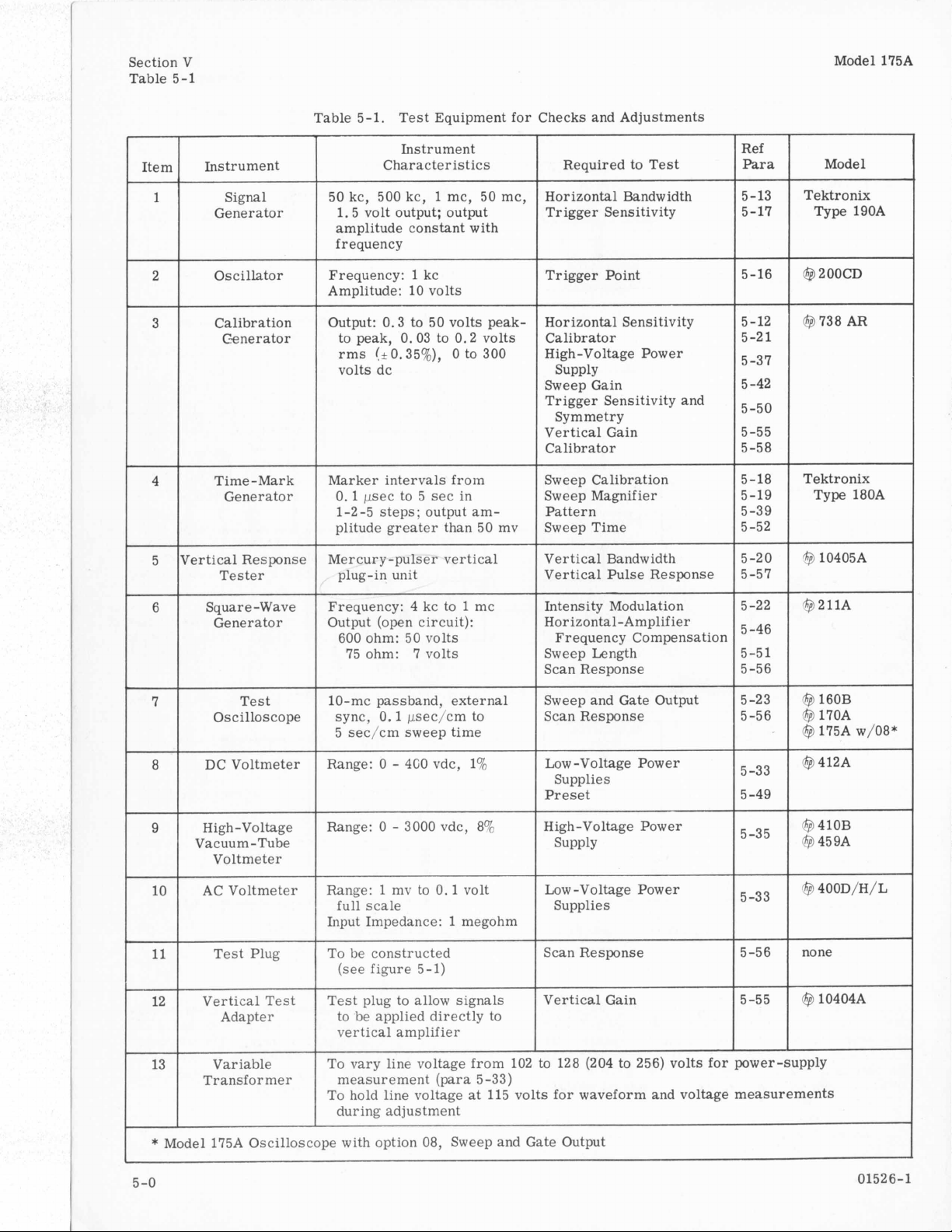
4-57.
A
simplified block diagram of the regulated output).
is
power supplies
regulator acts
each supply output (even
the return leg of the supply,
+370
volt returns, the regulator
shown in figure
as
a
variable resistance in series with output against a reference voltage. The amplifier
if
the series regulator
Figure
as
in the
is
DRIVER
DIFFERENTIAL
AMPL
I
FlER
V461
8
T
DRIVER
0402,4483
4-9.
Low-Voltage Power-Supply Block Diagram
4-9.
Each series
is
in then changes the effective resistance
+110
volt and regulator, and thereby the voltage drop across
in
series with the oppose the change in output voltage.
SENSOR
AMPLIFIER
0484
A
any change in the output voltage by comparing the
4
sensor or differential amplifier senses
w:
v
*’
A
-
BD-L-lll
b
-6.3V
b
+6.3V
of
the series
it,
to
01526-1
4-7
Page 26
Section
V
Table 5-1
Model 175A
~
Item
1
Instrument
~
'ertical Response
Table 5-1. Test Equipment for Checks and Adjustments
Instrument
Required to Test Mode 1
Horizontal Bandwidth
Trigger Sensitivity
Signal
Generator
~~~ ~
Characteristics
50 kc, 500 kc, 1 mc, 50mc,
1.5 volt output; output
amplitude constant with
frequency
Oscillator Trigger Point
Frequency:
1
kc
Amplitude: 10 volts
Calibration
Generator
Output: 0.3 to 50 volts peak-
0.2
0
to 300
volts
to peak, 0.03 to
rms (*0.350/0),
volts dc
Horizontal Sensitivity
Calibrator
High-Voltage Power
Supply
Sweep Gain
Trigger Sensitivity and
Symmetry
Vertical Gain
Calibrator
~~ ~
Time -Mark
Generator
Marker intervals from
0.1 psec to 5 sec in
1-2-5 steps; output am-
plitude greater than 50 mv
Sweep Calibration
Sweep Magnifier
Pattern
Sweep Time
Vertical Bandwidth
Tester
plug-in unit
Vertical Pulse Response
Ref
Para
5-13
5-17
5-16
5-12
5-21
5-37
5
-42
5-50
5-55
5-58
5-18
5-19
5-39
5-52
5-20
5-57
Tektronix
Type 19OA
@
200CD
@738 AR
Tektronix
Type 180A
9
10405A Mercury-pulser vertical
6
Square-Wave
Generator
Test
Oscilloscope
DC Voltmeter
9
High-Voltage
Vacuum -Tube
Voltmeter
10
11
AC Voltmeter
Test Plug
12 Vertical Test
Adapter
Frequency: 4 kc to
1
mc
Output (open circuit):
600 ohm: 50 volts
75 ohm:
7
volts
10-mc passband, external
sync, 0.1 psec/cm to
5 sec/cm sweep time
Range:
Range:
0
-
4CO
0 - 3000
vdc,
1%
vdc, 8%
full scale
Input Impedance:
To
be constructed
1
megohm
(see figure 5-1)
Test plug to allow signals
to be applied directly to
vertical amplifier
Intensity Modulation
Horizontal-Amplifier
Frequency Compensation
Sweep Length
Scan Response
Sweep and Gate Output
Scan Response
Low -Voltage Power
Supplies
Preset
High-Voltage Power
Supply
Low
-Voltage Power
Supplies
scan Response none
Vertical Gain
5-22
5-46
5-51
5-56
5-23
5-56
5-33
5-49
5-35
5-33
5-56
'@211A
$3
160B
$3
170A
@
175A w/08*
@
412A
'@
410B
\@
459A
$3
400D/H/L Range: 1 mv to 0.1 volt
@
10404A
13 Variable
Transformer
To vary line voltage from 102 to
measurement (para 5-33)
To
hold line voltage at 115 volts for waveform and voltage measurements
during adjustment
*
Model 175A Oscilloscope with option 08, Sweep and Gate Output
-0
5
128
(204 to 256) volts for power-supply
01526-1
Page 27
Model 175A
Paragraphs 5-1 to 5-12
Section
V
SECTION
MAINTENANCE
5
-1.
INTR
0
DU
CTION.
5-
2.
This section covers routine maintenance,
troubleshooting, and adjustment of the Model 175A
Oscilloscope.
may be used to verify proper operation of the instrument at incoming inspection or after adjustments
have been made.
5-3.
SERVICING THE AIR FILTER.
5-4. Inspect the
ment and clean
to restrict the flow of cooling
the
filter
in warm water and detergent. Dry thoroughly and
coat with a
from Research Products Company, Inc. This adhesive
your Hewlett-Packard sales representative.
5-5.
5-6. The performance check
mine whether or not the instrument
in
refer
horizontal plug-in units, refer to the individual manuals covering these instruments.
5-7. TEST EQUIPMENT.
5-8. Test equipment recommended for the per-
formance check
7.
istics may
5-9. PRELIMINARY SETTINGS.
5-10. Vertical and horizontal plug-in units must be
in place to make the performance check. Set the 115230 volt switch to the line voltage being used.
channel, select CHANNEL
trols. Make the following settings on the panel of
the vertical plug-in unit:
settings on the panel of the horizontal plug-in unit:
is
PERFORMANCE CHECK.
its
specifications. Should adjustment be required,
to paragraph 5-25.
Similar instruments having the listed character-
a.
If
the vertical plug-in unit
AC-DC..
SENSITIVITY
VERNIER
b.
Depending on model number, make the following
Model 1780A:
Model 1781A/B:
Model 1782A:
Model 1783A:
A
performance check
air
filter at the rear of the instru-
it
before
from the instrument and wash
filter
adhesive such
available from heating supply stores or from
is
listed in table 5-1, items 1 through
be
substituted.
it
becomes clogged enough
To check the vertical and
A
and use channel A con-
..................
..........
.................
SWEEP OCCURRENCE.
SWEEP SELECTOR
FUNCTION
TIME MARKER
.............
..........
is
included which
air.
To clean, remove
it
as
Filter Coat No. 3
is
intended to deter-
is
operating with-
has
more than one
2
VOLTS/CM
...
...
MAINSWEEP
thoroughly
AC
CAL
NORMAL
OFF
OFF
V
c. Make the following settings on the Model 175A:
POWER
INTENSITY MODULATION
SWEEP TIME
Sweep VERNIER
HORIZONTAL DISPLAY
EXTERNAL VERNIER
TRIGGER SOURCE
SWEEP MODE
TRIGGER LEVEL
TRIGGER SLOPE
d. Depress BEAM FINDER to locate trace. With
BEAM FINDER depressed, center display with horizontal and vertical position controls.
e. Release BEAM FINDER and turn INTENSITY
control clockwise,
pear on screen.
f.
The INTENSITY control should vary the intensity
of the display from extinguished to brighter than normal intensity. Adjust INTENSITY for normal viewing
level.
g. The FOCUS control should defocus the display
at each extreme of the control and focus the display
at approximately midrange. Adjust FOCUS for
sharpest display.
h. Adjust SCALE control to align the trace parallel
to the horizontal graticule lines.
5-11. HORIZONTAL AMPLIFIER.
5- 12. SENSITIVITY.
a. Connect the Calibration Generator to HORIZ
INPUT.
b. Set Calibration Generator output for 10 volts
peak- to-peak.
c. Set:
HORIZONTAL DISPLAY
EXTERNAL VERNIER. fully counterclockwise
d. Horizontal deflection should be
e. Set:
EXTERNAL VERNIER
f.
Horizontal deflection should be 10 cm k0.5 cm.
g. Set Calibration Generator output for
peak-to-peak.
h. Set:
HORIZONTAL DISPLAY
..................
....
.........
INTERNAL
1
MSEC/CM
.............
.........
.........
............
..........
FREE RUN
ON
CAL
X1
CAL
INT
.............
.............
if
necessary. A trace should ap-
. .
1
VOLT/CM AC
1
cm or less.
..........
.
0.1 VOLT/CM AC
1
(+)
CAL
volt
0
01526-1
5-1
Page 28
Section
Paragraphs 5-13 to 5-17
DISPLAY in the same manner.
5-13. BANDWIDTH.
amplitude for a horizontal deflection of
5-14. SWEEP GENERATOR.
5-15. PRESET.
vertical INPUT.
V
i.
Horizontal deflection should be 10 cm *0.5 cm.
j.
Check the two dc positions of HORIZONTAL
k. Disconnect Calibration Generator.
a. Connect Signal Generator to HORIZ INPUT.
b. Set:
HORIZONTAL DISPLAY.
c. Set Signal Generator for 50 kc and adjust output
d. Set frequency of Signal Generator to
e. Horizontal deflection should be at least 7 cm.
f.
Disconnect Signal Generator.
a. Set:
HORIZONTAL DISPLAY
SWEEP MODE
b. No sweep should be present.
c.
Connect CALIBRATOR 10 VOLT output to the
d.
A
stable synchronized display should be present.
e.
Disconnect CALIBRATOR.
*
*
.
0.1 VOLT/CM DC
.........
*
- * -
.
10
500
PRESET
cm.
kc.
X1
Model 175A
Set Signal Generator frequency to 1 mc and out-
c.
put amplitude for
Adjust TRIGGER LEVEL,
d.
synchronized display and reduce the Signal Generator
output amplitude until the sweep stops. The sweep
should continue to trigger at signal amplitudes 0.2 cm
or greater.
e. Set:
TRIGGER SOURCE
f.
Repeat steps c and d. The sweep should con-
tinue to trigger at signal amplitudes of approximately
0.5 cm or greater.
g. Set:
TRIGGER SOURCE
h. Repeat steps c and d. The sweep should con-
tinue to trigger at signal amplitudes of approximately
0.5 cm or greater.
i.
Set frequency of Signal Generator to
output amplitude for 3 cm of deflection.
j.
Set:
SWEEP TIME
HORIZONTAL DISPLAY
k. Repeat step d. The sweep should continue to
trigger at signal amplitudes of approximately
or greater.
m. Set:
TRIGGER SOURCE
1
cm of vertical deflection.
if
necessary, for a
.........
.........
.........
.........
0.1
.........
EXT
AC
EXTDC
50
mc and
pSEC/CM
X10
1
cm
EXT AC
5-16. TRIGGER POINT.
a.
Connect Oscillator to vertical INPUT.
b. Adjust Oscillator output for 5 cmdeflection, and
frequency to
c. Rotate TRIGGER LEVEL to bothextremes. The
starting point of the sweep should be adjustable to any
point
on
d. Set:
TRIGGER SLOPE
e. Rotate TRIGGER LEVEL to bothextremes. The
starting point of the sweep should be adjustable to any
point on the negative slope of the signal.
f.
Disconnect Oscillator. ReturnTRIGGER LEVEL
to
0
and TRIGGER SLOPE to
5-17. TRIGGER SENSITIVITY.
a. Connect Signal Generator to the verticalINPUT
and TRIG INPUT.
b. Set:
SWEEP TIME
Vertical SENSITIVITY
1
kc.
the positive slope of the signal.
.............
+.
..........
...
0.5
1
pSEC/CM
VOLT/CM
(-1
n. Repeat step d. The sweep should continue to
trigger at signal amplitudes of approximately
or greater.
p. Set:
TRIGGER SOURCE
q. Set Signal Generator output amplitude for 3 cm
of deflection.
r.
Repeat step d. The sweep should continue to
trigger at signal amplitudes of approximately
or greater.
s.
Disconnect Signal Generator.
t.
Connect a Model 10003A (AC-21M) Probe to
vertical INPUT.
u. Set:
TRIGGER SOURCE
Vertical SENSITIVITY
SWEEP TIME
HORIZONTAL DISPLAY
TRIGGER LEVEL
v. Connect probe tip to power line. Donot connect
probe ground lead.
...........
...........
....
.........
5 VOLTS/CM
5MSEC/CM
.........
.............
1
cm
INT
2
cm
LINE
X1
0
5-
2
01526-1
Page 29
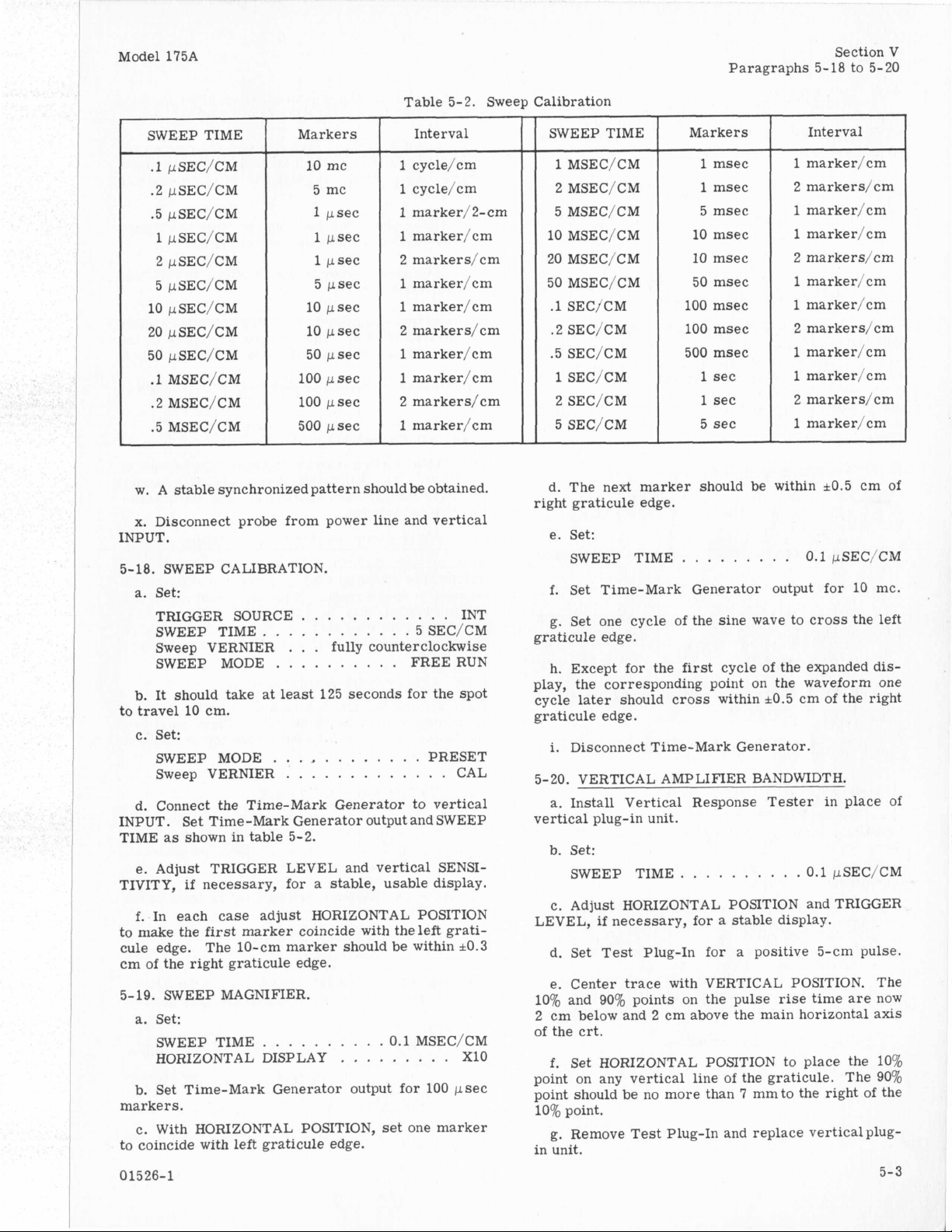
Model
175A
SWEEP TIME
.I
~SEC/CM
.2
FSEC/CM
.5
~SEC/CM
1
~SEC/CM
2
~SEC/CM
5
FSEC/CM
io
~SEC/CM
20
~SEC/CM
50
~SEC/CM
.I
MSEC/CM
.2
MSEC/CM
.5
MSEC/CM
Markers
10
mc
5
mc
1
psec
1
psec
1
psec
5
psec
10
psec
10
psec
50
psec
100
psec
100
psec
500
psec
Table
~~ ~
Interval
1
cycle/cm
1
cycle/cm
1
marker/2- cm
1
marker/cm
2
markers/cm
1
marker/cm
1
marker/cm
2
markers/cm
1
marker/cm
1
marker/cm
2
markers/cm
1
marker/cm
5-2.
Sweep Calibration
SWEEP TIME
1
MSEC/CM
2
MSEC/CM
5
MSEC/CM
io
MSEC/CM
20
MSEC/CM
50
MSEC/CM
.1
SEC/CM
.2
SEC/CM
.5
SEC/CM
1
SEC/CM
2
SEC/CM
5
SEC/CM
Paragraphs
Markers
1
msec
1
msec
5
msec
10
msec
10
msec
50
msec
100
msec
100
msec
500
msec
1
sec
1
sec
5
sec
Section
5-18
to
Interval
1
marker/cm
2
markers/cm
1
marker/cm
1
marker/cm
2
markers/cm
1
marker/cm
1
marker/cm
2
markers/cm
1
marker/cm
1
marker/cm
2
markers/cm
1
marker/cm
V
5-20
A
stable synchronized pattern should be obtained.
w.
x.
Disconnect probe from power line and vertical
INPUT.
5-18.
SWEEP CALIBRATION.
a.
Set:
TRIGGER SOURCE.
SWEEP TIME.
Sweep VERNIER
SWEEP MODE
b.
It should take at least
to travel
c. Set:
d. Connect the Time-Mark Generator to vertical
INPUT. Set Time-Mark Generator output and SWEEP
TIME as shown in table
e.
TIVITY,
f.
to make the
cule edge. The 10-cm marker should be within
cm
5-19.
a. Set:
b. Set Time-Mark Generator output for
markers.
c. With HORIZONTAL POSITION, set one marker
to coincide with
0
1526-
10
cm.
SWEEP MODE
Sweep VERNIER
Adjust TRIGGER LEVEL and vertical SENSI-
if
necessary, for a stable, usable display.
In each case adjust HORIZONTAL POSITION
first
marker coincide with theleft grati-
of
the right graticule edge.
SWEEP MAGNIFIER.
SWEEP TIME
HORIZONTAL DISPLAY
1
..........
left
graticule edge.
...........
...........
...
fully counterclockwise
..........
125
seconds for the spot
FREE RUN
............
.............
5-2.
0.1
MSEC/CM
.........
5
SEC/CM
PRESET
100
psec
INT
CAL
i0.3
XI0
d. The next marker should be within i0.5 cm of
right graticule edge.
e. Set:
SWEEP TIME
f.
Set Time-Mark Generator output for
g. Set one cycle of the sine wave to cross the left
graticule edge.
h. Except for the
play, the corresponding point on the waveform one
cycle later should cross within
graticule edge.
i.
Disconnect Time-Mark Generator.
5-20.
VERTICAL AMPLIFIER BANDWIDTH.
a. Install Vertical Response Tester in place of
vertical plug-in unit.
b. Set:
SWEEP TIME.
c. Adjust HORIZONTAL POSITION and TRIGGER
LEVEL,
d. Set Test Plug-In for a positive 5-cm pulse.
e. Center trace with VERTICAL POSITION. The
10%
2
cm below and 2 cm above the main horizontal axis
of the crt.
f.
point on any vertical line of the graticule. The
point should be no more than 7 mm to the right of the
10%
g. Remove Test Plug-In and replace verticalplug-
in unit.
if
necessary, for a stable display.
and
90%
points on the pulse rise time are now
Set HORIZONTAL POSITION to place the
point,
.........
first
cycle of the expanded dis-
.........
i0.5
0.1
cm
0.1
pSEC/CM
10
of
the right
pSEC/CM
mc.
10%
90%
5-3
Page 30
Section V
Paragraphs 5-21 to 5-32
Model 175A
5-21. CALIBRATOR.
a. Connect the Calibration Generator to vertical
INPUT and set output for 10 volts peak-to-peak.
b.
Set:
SWEEP TIME
HORIZONTAL DISPLAY
Vertical SENSITIVITY
Vertical Sensitivity
VERNIER
c. Rotate vertical sensitivity VERNIER clockwise
for exactly 5 cm of vertical deflection.
d. Disconnect Calibration Generator and connect
CALIBRATOR 10 VOLT output to vertical INPUT.
Vertical deflection should be
bient temperature
and 95°F). Vertical deflection should be 5 cm
cm
if
ambient temperature
or 35°C and 55°C (32°F and 50°F or 95°F and
130°F).
5-22. INTENSITY MODULATION.
a.
Connect the 600-ohm output of the Square Wave
Generator to vertical INPUT and INTENSITY MODULATION INPUT.
b. Set 600-ohm output to maximum and frequency
to 10 kc.
c. Set:
SWEEP TIME
Vertical SENSITIVITY
INTENSITY MODULATION.
Vertical POLARITY
d.
The top of the square wave should beintensified
with respect to the bottom.
e. Disconnect Square Wave Generator. Return
INTENSITY MODULATION to INT.
..........
2
.........
.....
..........
5
is
between 15°C and 35°C (50°F
is
between 0°C and 15°C
..........
....
1
counterclockwise
cm *0.05 cm
20 pSEC/CM
10 VOLTS/CM
.......
...........
MSEC/CM
X1
VOLT/CM
if
am-
*0.15
EXT
+UP
b. Connect the Model 10003A (AC-21M) Probe from
vertical INPUT to CALIBRATOR 10 VOLT output.
c. Loosen locknut
plastic flange with respect to cable. The waveform
should change from one with overshoot to one with
undershoot.
d. Adjust probe for best square wave and tighten
locknut.
e. Disconnect probe from vertical INPUT and
CALIBRATOR.
f.
to vertical INPUT. The vertical amplitude of the
display should be equal to that noted in step d.
g. Disconnect CALIBRATOR from vertical INPUT.
5-25. ADJUSTMENTS.
5-26. This section covers internal adjustments of
the Model 175A.
any adjustment, refer to paragraph 5-67 for troubleshooting procedures.
5-27. EQUIPMENT NEEDED FOR ADJUSTMENTS.
5-28. In table 5-1, items 3 through 13 are the test
instruments recommended to make the adjustments
outlined in this section. Equipment with equivalent
characteristics may be substituted. The special
horizontal Test Plug shown in figure 5-1
to test the main vertical amplifier scanner outputs.
5-29. LOCATION OF ADJUSTMENTS.
5-30.
and adjustments in the Model 175P.. These diagrams
are screened on the inside of the top and bottom
covers of the instrument.
Note vertical amplitude of display.
Connect CALIBRATOR 1 VOLT output directly
Figures 5-2 and 5-3 show the location of tubes
at
rear of probe and rotate rear
If
difficulty
is
encountered in making
is
required
5-23. SWEEP AND GATE OUTPUT
(OPTIONAL FEATURE).
a.
Set SWEEP MODE to FREE RUN.
b. Trigger Test Oscilloscope with gate output
signal from Model 175A.
c. Observe SWEEP OUTPUT signal on Test
cilloscope.
imately -2.5 to +2.5 volts on
settings.
d. Observe GATE OUTPUT signal on Test Oscilloscope. Signal should be approximately
the duration of sweep on all SWEEP TIME settings.
e. Disconnect Test Oscilloscope.
5-24. ACCESSORY PROBES.
a.
Set:
SWEEP TIME
Vertical SENSITIVITY
5-4
Signal should be a linear ramp of approx-
.........
all
...
0.2 VOLTS/CM
SWEEP TIME
4
0.5 MSEC/CM
Os-
volts for
5-31. PRELIMINARY SETTINGS.
5-32. Install vertical and horizontal plug-in units
in their compartments in the Model 175A. If the
vertical plug-in unit has more than one channel,
select CHANNEL
a. Make the following settings on the panel of the
vertical plug-in unit.
AC-DC..
VERNIER
b.
Depending on model number, make the follow-
ing settings on the panel of horizontal plug-in unit:
Model 1780A:
SWEEP OCCURRENCE.
Model 1781AjB:
SWEEP SELECTOR
Model 1782A:
FUNCTION
Model 1783A:
TIME MARKER.
A
and use channel A controls.
.................
.................
..
.NORMAL
...
MAIN SWEEP
...........
........
AC
CAL
OFF
OFF
01526-1
Page 31

Model 175A
J105(13)<<
T
RI
IOOK
Paragraphs 5-33 to 5-39
d.
Check regulation of each supply
age
is
varied between 102 and 128 volts.
voltages should remain within
in step b or c.
e.
Measure
Voltmeter.
given in table 5- 3.
ac
ripple on each supply using the AC
The ripple should be within the values
Section
as
the line volt-
All
regulated
1%
of the values noted
V
J
1050
5)<<
RI.
1/2W, -hp-STOCK N0.0727-0304
1
R2: RESISTORS, IOOK f lolo,
\
CONNECTOR: MALE, 32-PIN,
AMPHENOL PART NO. 26-4100-32P
-hp- STOCK NO. 1251-0136
Figure 5-1. Test Plug
R2
IOOK
I
CI. C2: CAPACITORS, IOPF
f
0.5PF, 500V,-hp- STOCK
NO.
0150-0009
LD-S-bm
Wire
Supply Tolerance Ripple
(volts) (volts) (rms) Code
-
100 *3 3 mv
+110 *3 3mv pink
+370
+6.3
-6.3
5-35. HIGH-VOLTAGE POWER SUPPLY.
5-36. Refer to
5-37. DC OUTPUT.
a.
b.
meter by setting ,the Calibration Generator to 300
volts, connecting the voltmeter 100:
divider probe to the generator output, and setting the
Voltmeter to read 3 volts.
*lo
*.2
*.2 2
Set line voltage to 115 volts.
Calibrate the High-Voltage Vacuum-Tube Volt-
4 mv red
2 mv brown
mv grav
figure
5-2 for location of adjustments.
Color
violet
Adjust-
ment
R472
R45
R433
R486
R486
1
high-voltage
1
c.
Connect Model 175A to power source through
Variable Transformer and
volts. Make the following settings on thepanel of the
Model 175A:
POWER
HORIZONTAL DISPLAY
EXTERNAL VERNIER
TRIGGER SOURCE
TRIGGER SLOPE
TRIGGER LEVEL
SWEEP MODE
SWEEP TIME
Sweep VERNIER
5-33. LOW-VOLTAGE POWER SUPPLIES.
5-34. Refer to figure 5-3 for location of adjustments.
a. Set line voltage to 115 volts (230voltsif the 115-
230 volt switch
b.
Measure output of each supply connecting the
DC Voltmeter to the terminals on the printed circuit
board mounted adjacent and at right angles to the
supply fuses (see figure 5-3).
c.
The voltages
given
in
the adjustments in the order given in table 5-3.
01526-1
..................
is
in 230-volt position).
table 5-3. If adjustment
will
set
line voltage to 115 (230)
. .
1
VOLT/CM AC
.........
...........
............
.............
...........
.........
.............
normally be within the limits
is
PRESET
lMSEC/CM
required, make
ON
CAL
INT
(+)
CAL
0
c.
Set Voltmeter range to 30 volts and measure the
voltage
T401 (see figure 5-3).
*loo
ing of -2700 volts.
-2700 volt supply output should remain within *25
volts of the reading obtained in step d or
5-38. ASTIGMATISM.
tain the smallest round and sharply focused spot.
5-39. PATTERN.
INPUT.
at
pin 1 of the low-voltage power transformer
d. The measured voltage should be -2790 volts
volts.
e.
Adjust
f.
Vary line voltage from 102 to 128 volts. The
a.
Center a low intensity spot on the crt.
b. Adjust FOCUS and Astigmatism Adj R340 to ob-
a. Connect the Time-Mark Generator to vertical
b.
Set:
HORIZONTAL DISPLAY
HV
Adj R328,
if
necessary, for a read-
e.
.........
X1
5-5
Page 32

Section
Figure
V
5-2
Model 175A
@
6CW5
DELAY LINE
a
TRANSFORMER
I
,=
I
?
I
HORIZ. BLU.
GRN. VERT.
122 MID FREQ. RESPONSI
-
cC36 SCAN, RESPONSE
LOW
:35
FREQ. RESPONSE
VERTICAL AMPLIFIER
-
V11 6DJ8
-
5
-6
+
R375 CAL. VOLT ADJ.
Q301
Q302
1
Figure 5-2. Adjustment and Component bcations,
Top
View
01526-1
Page 33

Model
175A
LOW VOLTAGE POWER SUPPLY
0
OQ433
OQ444
Q462
Q421
Section
Figure
7
-2700V
PIN #1
POWER TRANSFORMER
V
5-3
3AM COVER
UTPUT LEAD
MP. CONNEl
ED SWEEP
TO HORIZ
CTS
HERE
R433 t370V ADJ.
OQ424 OW64
0
0
~425
~463
I_.
(2x3
-
-
’
f
t
R472 -1OOV ADJ.
0
~484
@z8tv
ADJ.
::‘
EC
RED t370V--o
PINK
BROWN
VIOLET
+
llOVd*
t6.3V-•
-100V-•
GRAY,,
-6.3V
I
I
IO
lo
I
0
421
SAMP
441
LAMP
481
,AMP
I-EL0
461
LAMP
-
v
0
I
i
I
‘z
In
I\
c
01526-1
Figure
5-3.
Adjustment and Component Locations, Bottom View
5-7
Page 34

Section
Paragraphs 5-40 to 5-42
V
Model 175A
c.
Set Time-Mark Generator output to 5 mc and
adjust vertical SENSITIVITY and VERTICAL POSITION for a 6-cm display coinciding with top and bottom lines of graticule.
d. Set HORIZONTAL POSITION to align left side
of display with left graticule edge.
e.
Adjust Pattern Adj R345 for minimum barreling or pin-cushioning around top, bottom, and
sides of display
f.
Adjust HORIZONTAL POSITION to align right
side of display with right graticule edge.
g. Trim Pattern Adj R345,
e
for squarest overall pattern.
and
h. Disconnect Time-Mark Generator.
5-40. HORIZONTAL AMPLIFIER.
5-41. Refer to figure 5-3 for location of adjustments.
(see
figure 5-4).
if
necessary, for min-
Repeat steps d imum barreling or pin-cushioning.
left
5-42. SWEEP GAIN.
a.
Locate foam-covered wire which connects sweep
generator output to horizontal amplifier input (see
figure 5-3).
b.
Disconnect wire from sweep generator printed
circuit board.
c.
Set:
HORIZONTAL DISPLAY
d. Connect the Calibration Generator to the foam-
covered wire and
e. Center display and adjust X1 Gain Adj R225 for
5.5 cm of horizontal deflection.
f.
Set:
HORIZONTAL DISPLAY
g. Set Calibration Generator output to 5 volts peak-
to-peak.
set
output to 50 voltspeak-to-peak.
.
. . . . . .
.
.
. . . . .
.
.
XI0
X1
--
i-r
1
,;it
i-
BARRELING
*-
t
t
.
_-
PIN-CUSHIONING
WF-S-388
5-8
Figure 5-4. Pattern Adjustment
01526-1
Page 35

Model 175A
Paragraphs 5-43 to 5-46
Section V
h. Center display and adjust X10 Gain Adj R227 for
5.5 cm of horizontal deflection.
i.
Disconnect Calibration Generator from foam-
covered wire.
5-43. INTERNAL BALANCE.
a.
Set:
HORIZONTAL DISPLAY
SWEEP MODE
b.
Center the spot on
SITION control.
c.
Set:
HORIZONTAL DISPLAY
d. Adjust Magnifier Centering R230 to center spot.
e.
Repeat steps a through d until spot does not
move when switching HORIZONTAL DISPLAY from
x1
to x10.
5-44. EXTERNAL BALANCE.
a.
Set:
HORIZONTAL DISPLAY 0.1 VOLT/CM DC
EXTERNAL VERNIER fully counterclockwise
....
.........
just out of PRESET
crt
with HORIZONTAL PO-
.........
XI0
X1
d. Set:
Vertical SENSITIVITY
Vertical Sensitivity VERNIER
Vertical AC-DC.
HORIZONTAL DISPLAY
TRIGGER SOURCE
SWEEP MODE.
SWEEP TIME
e.
Set 600-ohm and 75-ohm Square-Wave Gener-
ator outputs to maximum and frequency to 4 kc.
f.
Center display and adjust TRIGGER LEVEL,
necessary, for a stable
...........
.........
....
.............
lOVOLTS/CM
.....
CAL
AC
.........
.........
display (see figure 5-5).
0.1
MSEC/CM
EXT AC
PRESET
X1
if
b.
Center the spot on
SITION control.
c.
Set:
EXTERNAL VERNIER
d. Adjust External Balance R212 to center spot.
e.
Repeat steps a through d until spot does not
move when EXTERNAL VERNIER
5-45. EXTERNAL GAIN.
a.
Connect Calibration Generator to HORIZ INPUT.
b.
Set:
HORIZONTAL DISPLAY
c.
Set Calibration Generator output to 1 volt peak-
to-peak.
d. Adjust Gain Adj R213 for 10 cm of horizontal
deflection.
e.
Disconnect Calibration Generator.
5-46. FREQUENCY COMPENSATION.
a.
Connect Square Wave Generator 600-ohm output
to foam-covered wire disconnected in paragraph 5-42.
b.
Connect 75-ohm output to TRIG INPUT.
c.
Connect, with a jumper, the vertical
the point (sweep output) on sweep-generator printed-
circuit board from which the foam-covered
disconnected
.
crt
with HORIZONTAL PO-
..........
is
rotated.
0.1 VOLT/CM DC
.
INPUT
wire
CAL
to
was
Figure 5-5. Frequency Compensation
g. Adjust Input Attenuator Compensation C211 for
best
square wave.
h. Set:
HORIZONTAL DISPLAY.
i.
Adjust 600-ohm Square Wave Generator output
for
8
cm of deflection. Trim C211,
for
best
square wave with HORIZONTAL DISPLAY in
X1 and X10 positions.
j.
Set:
HORIZONTAL DISPLAY.
SWEEP TIME
k. Set 600-ohm Square Wave Generator output to
maximum and frequency to 40 kc.
m. Adjust X1 Gain Compensation C213 for
square wave.
n. Set:
HORIZONTAL DISPLAY
p. Set 600-ohm Square Wave Generator output for
8
cm of deflection.
q. Adjust X10 Gain Compensation C212 for best
square wave.
r.
Set:
HORIZONTAL DISPLAY.
.........
........
if
necessary,
.........
10 gSEC/CM
.........
1
VOLT/CM DC
..
XI0
X1
best
XI0
01526-1
5-9
Page 36

Section
Paragraphs 5-47
V
to
5-50
Model 175A
5-50. TRIGGER SENSITIVITY AND SYMMETRY.
a.
Set:
SWEEP MODE
TRIGGER SLOPE
TRIGGER SOURCE
HORIZONTAL DISPLAY
SWEEP TIME.
Vertical SENSITIVITY.
Vertical AC-DC
b.
Connect Model 10003A (AC-21M) Probe from
vertical INPUT to case of tunnel diode CR102 on
sweep-generator circuit board (see figure 5-3).
CAUTION:
+110
...........
.............
.........
.........
.........
..
0.05 VOLT/CM
.............
VOLTS present at this point.
PRESET
(-)
EXT AC
X1
lMSEC/CM
AC
Figure 5-6. Attenuator Compensation
(Top: undercompensated, Middle: compensated,
Bottom: overcompensated)
s.
Disconnect 600-ohm Square- Wave Generator
output from foam-covered wire and connect Generator
to HORIZ INPUT. Adjust output amplitude for 8 cm
deflection and frequency to
t.
Adjust Attenuator Compensation C203 for round
dots with no tails (see figure 5-6).
u. Disconnect Square- Wave Generator and jumper
from vertical INPUT and sweep-generator printedcircuit board. Connect foam-covered wire to sweepgenerator printed-circuit board.
5-47. SWEEP GENERATOR.
5-48. Refer to figure 5-3 for location of adjustments.
5-49. PRESET.
a.
Set:
HORIZONTAL DISPLAY
SWEEP TIME
b.
Connect DC Voltmeter to pin 3 of V109. This
voltage will be approximately -40 volts.
c.
Rotate SWEEP MODE slowly clockwise while
watching Voltmeter.
sweep generator free runs.
d. Note voltage at which sweep generator free runs
(maximum negative reading obtained on Voltmeter).
e.
Set:
SWEEP MODE.
f.
Adjust Preset Adj R170 for meter reading of
2.5 volts less negative than voltage noted in step d.
g. Disconnect Voltmeter.
4
kc.
.........
.........
Meter pointer
will
...........
X1
10 pSEC/CM
jump when
PRESET
c. Connect Calibration Generator to TRIG INPUT
and adjust output for 0.05 volt rms.
d. Mechanically center Trigger Symmetry R116,
and turn Trigger Sensitivity R120 fully clockwise.
e. Rotate TRIGGER LEVEL to obtain a free running display approximately 0.5 volt in amplitude (see
figure 5-7).
Figure 5-7. Trigger Sensitivity
(Top: Synchronized, Bottom: Free Running)
f.
Using TRIGGER LEVEL to maintain a presen-
tation adjust Trigger Sensitivity R120 counterclock-
wise until a stable, synchronized, symmetrical
square wave approximately 0.35 volt in amplitude
obtained (see figure 5-7).
g. Set Calibration Generator output to 0.03 volt rms.
h. The trigger circuit should not trigger solidly.
Counterclockwise adjustment of Trigger Sensitivity
R1-20 may be necessary to prevent solid triggering.
Rotate TRIGGER LEVEL when checking for solid
triggering.
i.
Set Calibration Generator output to 0.05 volt rms.
j.
The trigger circuit should again trigger solidly.
Adjust TRIGGER LEVEL
f,
g, h, and i until circuit triggers solidly with a
0.05-volt rms input and does not trigger solidly with
a 0.03-volt rms input.
if
necessary. Repeat steps
<L
is
5-10
01526-1
Page 37

Model 175A
Section V
Paragraphs 5-51 to 5-56
.k. Set:
TRIGGER SLOPE
m. Ground green/orange wire which
to TRIGGER SLOPE switch.
n. Adjust Trigger Symmetry R116 for
rical square wave display.
p. Unground greedorange
from CR102 and vertical INPUT. Disconnect Cali-
bration Generator.
5-51. SWEEP LENGTH.
a.
Connect Square-Wave Generator 75-ohm output
to vertical INPUT, and set frequency to
b. Set:
HORIZONTAL DISPLAY.
TRIGGER SOURCE..
TRIGGER LEVEL
SWEEP MODE
SWEEP
c.
Set Square Wave Generator output and vertical
SENSITIVITY for approximately 3 cm of deflection.
d. Adjust Sweep Length R161 for
TIME.
...........
.........
wire.
........
..........
.............
is
connected
a
symmet-
Disconnect probe
1
mc.
X1
INT
PRESET
1
MSEC/CM
11
cm of sweep.
0
5-53.
5-54. Refer to figure 5-2 for locationof adjustments.
5-55. GAIN.
a. Install Vertical Test Adapter in vertical plug-in
connector
b.
Generator to Test Adapter and adjust position con-
trol on adapter for on-scale trace.
c. Adjust Gain R45 for 5 cm deflection.
d.
in unit.
5-56. SCAN RESPONSE.
a. Connect Square-Wave Generator 75-ohm output
to vertical INPUT and set frequency to 50 kc.
b.
vertical SENSITIVITY for 6 cm of deflection.
c. Trigger Test Oscilloscope with 600-ohm output
of Square- Wave Generator.
d.
and install Test Plug described in paragraph 5-28.
51
in place of vertical plug-in unit.
Connect 1.0 volt peak-to-peak from Calibration
Remove Test Adapter and install vertical plug-
Set Square-Wave Generator 75-ohm output and
Remove horizontal plug-inunit from Model 175A
e.
Disconnect Square-Wave Generator.
5-52. SWEEP TIME.
a. Connect Time-Mark Generator to vertical
INPUT.
b.
Set:
HORIZONTAL DISPLAY
SWEEP MODE
TRIGGER SOURCE
c. Set vertical SENSITIVITY andTRIGGER LEVEL
for
a
suitable display, and set SWEEP TIME and
marker interval as shown in table 5-4.
corresponding adjustment for the indicated markers
per centimeter
d. Disconnect Time-Mark Generator.
Table 5-4. Sweep Time
SWEEP TIME
.I
~SEC/CM
.2
FSEC/CM
.5
USEC/CM
1
~SEC/CM
io
~SEC/CM
.I
MSEC/CM
1
MSEC/CM
io
MSEC/CM
.I
SEC/CM
...........
if
necessary.
Markers
10 mc
5 mc
1
psec
1
psec
10 psec
100 psec
1
msec
10 msec
100 msec
..........
PRESET
...........
Make
1
Adjust
C125
C1016
C1014
C1012
ClOlO
R1005
R1004
R1003
R1002
Set for
1
cycle/cm
1
cycle/cm
1
marker/2 cm
1
marker/cm
1
marker/cm
1
marker/cm
1
marker/cm
1
marker/cm
1
marker/cm
X1
INT
the
e.
Observe signal on pin 15 of horizontal plug-in
Use
connector 5105.
minimize loading.
f.
Adjust Scan Response C36 for best square wave
as
viewed on Test Oscilloscope.
g. Observe signal on pin 13 of horizontal plug-in
connector 5105.
h. Adjust Scan Response C37 for best square wave
as viewed on Test Oscilloscope.
i.
Set frequency of Square-Wave Generator to 1 mc.
j.
Observe signal on pin 10 of Test Plug.
k. Adjust Scan Balance C33 for best balance as
viewed on Test Oscilloscope (see figure 5-8).
Figure 5-8. Scan Balance (Top: Unbalanced
Middle: Balanced, Bottom: Unbalanced)
probe on Test Oscilloscope to
01526-1
5-11
Page 38

Section
Paragraphs 5-57 to 5-60
Generator.
in
5-57. PULSE RESPONSE.
Plug-In Unit.
5 cm
just
of pulse about 0.2 cm (see figure 5-9).
v
m.
Disconnect Test Oscilloscope and Square-Wave
n. Remove Test Plug and install horizontal plug-
unit.
a.
Remove vertical plug-in unit and install Test
b.
Set Test Plug-In
in
amplitude.
c.
Set:
SWEEP TIME.
TRIGGER SOURCE
TRIGGER SLOPE
SWEEP MODE
HORIZONTAL DISPLAY
d. Set TRIGGER LEVEL for stable displayandad-
Mid Freq. Response C22 to drop leading corner
Unit
for a positive pulse output
........
-
-
-
*
0.5 pSEC/CM
* * *
............
* * - * * * * *
*
*
-
*
*
*
*
*
*
PRESET
*
- -
*
INT
(+)
X1
Model 175A
b. Set:
HORIZONTAL DISPLAY.
SWEEP TIME
TRIGGER SOURCE
TRIGGER LEVEL
SWEEP MODE.
Vertical SENSITIVITY
c.
Set vertical sensitivity VERNIER for exactly
6 cm of deflection.
d. Disconnect Calibration Generator and connect
vertical INPUT to CALIBRATOR 10 VOLT output.
e. Adjust Cal Volt Adj R375 for exactly 6 cm of
deflection.
f.
Disconnect CALIBRATOR from vertical INPUT.
.........
...........
.........
0.5 MSEC/CM
...........
X1
INT
.............
PRESET
.....
1
VOLT/CM
0
Figure 5-9. Mid-Frequency Response
Preliminary Adjustment
e.
Adjust Low Freq Response C35 for
flat
top.
f.
Readjust Mid Freq Response C22 for bestpulse
response
g.
h. Adjust
high frequency corner (see figure 5-11).
i.
5-58. CALIBRATOR.
a.
and
(see
figure 5-10).
Set:
SWEEP TIME
Hi
Remove Test Plug-In and install vertical plug-in.
Connect Calibration Generator to verticalINPUT
set
output to 10 volts peak-to-peak.
.........
Freq Response L7 and L8 for best
0.1
best
pulse
pSEC/CM
Figure 5-10. Mid-Frequency Response
Final Adjustment
Figure 5-11. High-Frequency Response
5-59.
5-60. The Model 175A uses edge-on connectors for
most connections to the boards. The assembly may
be removed in a few moments for access to otherwise
hidden components. When removing or replacing
edge-on connectors be careful to align the connector
properly with
connector improperly aligned may spring the contacts
and result in a poor connection.
REPAIRS.
its
guide slot. Applying force with the
5-12
01526-1
Page 39

Model 175A
Section V
Paragraphs 5-61 to 5-73
5-61. EQUIPMENT REQUIRED.
5-62. In general, miniaturized equipment
miniature tools. The following
important:
a.
Low-heat soldering iron (25 to 50 watts). Idling
temperature must
b.
Small soldering iron tip (1/16 to 3/32 inch).
c.
Small-diameter rosin-core solder.
d. Wooden toothpick.
5-63. The low-heat iron
tect
solid-state devices from too high a temperature,
and to avoid causing conductors to
circuit boards. The small tip
to the component, yet will be adequate to melt the
solder. Small-diameter solder melts more quickly,
reducing the length of time
The toothpick
holes after removing a component.
repairs on the Model 175Aunless the above equipment
is
on hand.
5-64. PROCEDURE.
5-65. The Model 175A
boards. Each component mounting hole
through in order to provide electrical conduction from
one side of the board to the other and to provide
better solder bond between the circuit and the component. The plating
the hole with
leads into the hole. The use
for cleaning out solder, and ordinary care in replacing
the component, will result in a satisfactory job.
5-66. REPLACINGTRANSISTORS. Solid-state diodes
and
transistors require special handling, in
are
sensitive to both heat and electrical overload.
Use
long-nose pliers between the iron and the device
as
a
heat sink. Hold the pliers for a moment
the iron
there
leakage can damage transistors.
5-67.
5-68. ISOLATING TROUBLES TO A MAJOR
5-69. The following check may be performed whenever instrument malfunction
plug-in
is
removed
is
no electrical leakage from iron to work. Such
TROUBLESHOOTING.
SECTION.
a.
Set:
HORIZONTAL DISPLAY
EXTERNAL VERNIER
Vertical SENSITIVITY
Vertical
b.
Depending on the model number of the horizontal
unit,
be
no more than
is
required in order to pro-
that
is
essential for cleaning out mounting
has
is
easily damaged by reaming
a
metal tool, or by forcing component
to
allow the joint to cool. Be sure
is
Sensitivity VERNIER.
set
controls
as
follows:
are
800°F.
lift
from the printed
will
transfer less heat
heat mustbe applied.
plated-through circuit
of
the wooden toothpick
suspected.
,
.
1
..........
...
calls
for
particularly
Do
not attempt
is
plated
that
they
after
VOLT/CM AC
2 VOLTS/CM
.....
CAL
CAL
Model 1780A:
SWEEP OCCURRENCE
Model 1781A/B:
SWEEP SELECTOR.
Model 1782A:
FUNCTION.
Model 1783A:
MARKER
c.
Depress BEAM FINDER.
d.
A
defocused spot should appear on the crt.
e.
If
proper display
the power supplies are operating properly. If no spot
appears, troubleshoot
5-70 and 5-77) and the amplifiers (paragraphs 5-81
and 5-93).
f.
Connect CALIBRATOR
tical INPUT and HORIZ INPUT,
A
tilted straight line pattern with a 10-cm hori-
g.
zontal deflection and 5-cm vertical deflection should
be obtained.
h.
If
the horizontal amplifier, vertical amplifier, and calibrator are operating properly.
a
should be obtained.
the sweep generator
5-70. LOW-VOLTAGE POWER SUPPLIES.
5-71. The transistors used in the power supply are
located on the power-supply printed-circuit board and
fan-shroud assembly. The series-regulator tran-
sistors are power transistors mounted on heat sinks
on the fan-shroud assembly. The amplifier and other
transistors are mounted on the printed circuit board
(figure 5-33).
5-72.
required,
ment by removing the mounting screws on rear gusset.
However, power supply malfunctions can generally
quickly
circuit board or on the fan-shroud assembly, thus
eliminating unnecessary removal of the fan-shroud
ass e mbly
5-73. Nominal voltages
are given on the Low-Voltage Power-Supply schematic
diagram, figure 5-34.
proper display
i.
Set:
HORIZONTAL DISPLAY.
SWEEP MODE
SWEEP TIME
Sweep VERNIER
TRIGGER LEVEL
TRIGGER SOURCE
j.
A
synchronized square wave pattern 5 cm high
k.
If
proper display
If
maintenance on the fan-shroud assembly
it
may easily be removed from the instru-
be
isolated to components either on the printed
.
...........
............
is
obtained,
the
power supplies (paragraphs
10
is
obtained,
...........
..........
............
.............
...........
is
obtained,
is
operating properly.
at
key points in the supply
...
NORMAL
.
MAIN
SWEEP
OFF
OFF
it
is
likely
that
VOLT output to ver-
it
is
likely that
.........
1
MSEC/CM
it
is
likely
X1
PRESET
CAL
INT
that
-
is
0
01526-
1
5-13
Page 40

Section V
Paragraphs 5-74 to 5-76
Model 175A
5-74. The cause of excesr-re output ripple on any of
the supplies can
Measure the ripple at the output of the rectifiers of
the supply in question. Compare the measurement
with the value given on the schematic diagram, fig- supply outputs and ground
ure 5-34. If the ripple
filter capacitors and bleeder resistors. If the input
ripple
is
normal, the cause
&-amplifier transistors.
supply
-loov
be
isolated in the following manner.
Symptom
High output
Low output
is
excessive, check
is
most likelylow gain in anced output voltage can usually be traced to an open
Table 5-5.
Disconnect base lead of Q461 from
printed circuit board.
yellow lead which connects to rear
edge of board adjacent to fan motor.
Reconnect yellow
circuit board and short collector
of Q464 to emitter.
~ ~~ ~~~ ~~~
Short collector of Q462 to emitter I Output remains low I Q461 open
Remove short from Q462 and meas-
ure voltage across CR465
the
input load. The load
Troubleshooting the Low-Voltage Supply
Procedure
This
wire
to printed
5-75. T
cating causes of loss of regulation in each supply.
5-76. The balance between the +6.3 volt and -6.3volt
tube
or shorted tube heater or a wrong type
is
the
ble 5-5 gives troublesh
is
a series-parallel arrangement of
heaters, diagrammed in figure 5-35. An unbal-
Effect Trouble
Output remains high Q461 shorted
Voltage drops Q461 good
Output remains high Q462 shorted
Voltage drops Q464 open
I
Voltage rises
0
volt
6 volts
oting
aids
for lo-
is
determinedby the supply
I
Q461 good
CR465 shorted
CR465 good
tube.
I
I
+llOV
High output
Low output
Measure voltage across R470
Measure voltage from collector of
Q464 to emitter
Check -100 volt supply output
Disconnect base lead of Q442 from
printed circuit board. This
white lead which connects to rear
edge of board adjacent to fan motor.
Reconnect white lead and measure
voltage from collector of Q443
to emitter
Measure voltage from collector of
Q444 to emitter
Check -100 volt supply output
is
the
Within 10 volts of
output
Less than output
0
volt
approx 10 volts Q464 good
Normal Trouble in +llOV
0
volt Q443 shorted
Greater than
0
volt Q444 shorted
Greater than
Normal Trouble in
2
volts
2
volts
Q463 open or C466
shorted
Q463 and C466
good
Q464 shorted
Q441 and Q442 good
Q443 good
Q444 good
+llOV
Trouble in -1lOV
5-14
__~~~
Short collector of Q443 to emiiter
~
~~ ~
Output remains low
Voltage rises
Q441 or Q442 open
Q441 and Q442 good
01
5
26-
1
Page 41

Model
+
llOV
cont'd
+
370V
175A
~~
Symptom
Low output
High output
Table
5-5.
Troubleshooting the
Procedure Effect
Remove short from
collector of
Remove short from
ure voltage
Check
Check
-100
+
Q444
at
base
volt supply output
~~~~ ~
110
volt supply output
Low
Q443
and short No change
to emitter
Q444
and meas-
of
Q444
-Voltage Supply (Cont'd)
Voltage rises
Positive
Normal
Abnormal
Table
5-5
I
Trouble
Q443
open
Q444
open
C445
shorted or
leaky
~~ ~~ ~
Trouble in
+
370V
Trouble in
supply
Trouble in
+
supply
-lOOV
+
Section
(cont'd)
llOV
370V
V
or
Low output
Disconnect base lead of
printed circuit board. This
orange lead which connects
rear
edge of board adjacent to
fan motor.
Reconnect orange lead and meas-
ure voltage from collector
Q424
to emitter
Measure voltage from collector
of
Q425
to emitter
-100
Check
Check
Short collector of
Remove short from
ure voltage across
volt supply output Normal
+
110
volt supply output
Q424
Q424
CR425
Q423
from
is
to emitter
and
meas-
below
+
370
0
volt
Greater than
0
volt
Greater than
Normal
Abnormal
Output remains low
~~
Output
rises
I
0
volt
6
volts
volts
2
volts
2
volts
Q423
good
Q424
shorted
Q424
good
Q425
shorted
-25
good
Trouble in
Trouble in
supply
Trouble in
supply
Q421, Q422,
9423
open
Q421, Q422,
I
a23
good
CR425
CR425
shorted
good
+
110
+
370V
+
llOV
or
or
or
*6.3V
01526-1
High output
(Voltmeter
from
+
6.3V
to
-6.3V
output)
Short collector of
Check
Disconnect base lead of
-100
printed circuit board. This
blue lead which connects
edge of board adjacent to
the
5651
reference tube.
Q425
to
volt supply output
Q482
emitter
from
is
to
front
V461,
Output remains low
Output rises
Normal
Abnormal Trouble in
the
Output drops
Q424
open
Q425
open
Trouble in
supply
supply
shorted
+6.3V
-1OOV
5-15
Page 42

Section
Paragraphs 5-77 to 5-85
V
Model 175A
supply
*6.3V
cont’d
Symptom
Low output
(Voltmeter
from +6.3V
to -6.3V
output)
ble 5-5.
T
Reconnect blue
voltage from collector of Q483
to emitter
Short collector of Q484 to emitter
Check -100 volt supply output
Short collector of Q483 to emitter
Remove short from Q483 and meas-
ure voltage from collector of
Q483 to emitter
Measure voltage from collector of
Q484 to emitter
Measure voltage across CR483
Troubleshooting the Low-Voltage Supply (Cont’d)
Procedure Effect
wire
and measure
Trouble
0
volt
Greater than
Output drops
Normal
Abnormal Trouble in
Output remains low Q481 or Q482 open
Output
Greater than 10 volts Q483 open
Approx 2.5 volts Q483 good
0
volt Q484 shorted
Greater than
0
volt CR483 shorted
6 volts CR483 good
rises
2
volts
2
volts
Q483 shorted
Q483 good
Q484 open
Trouble in *6.3V
supply
-1OOV
supply
Q481 and Q482 good
Q484 good
5-77. HIGH-VOLTAGE POWER SUPPLIES.
5-78. Waveforms and dc voltages are given
troubleshooting aid on the high-voltage power-supply
schematic diagram, figure 5-32.
5-79. The cause of an output voltage whichis too high
or too low can best be isolated by measuring dc voltages. Start with the resistor divider string composed
of resistors R328 through R337. Then checkvoltages
on regulator tube V306 and
5-80. The cause of loss of regulation can also best
be
isolated by
ode voltage in the positive direction should be sensed
by V306 and appear
grid, pin 9, of V301. Theplatevoltage of V301 should
then increase accordingly. Likewise,
change in crt cathode voltage should cause the plate
voltage of V301 to decrease.
5-81. VERTICAL AMPLIFIER.
5-82.
As
and signal waveforms are given
amplifier schematic diagram, figure 5-19.
5-83. UNBALANCE. Unbalance
differential amplifier Vl-V4 and V7-V9 can be isolated
by
measuring the dc voltages on the various tube
elements.
unbalance in the vertical plug-inunit, short pins
7 of
V1
ential amplifier has equal voltages on each side of the
amplifier, another method may be used to isolate an
unbalanced stage. Proceed
this
method. A changein the crt cath-
as
a troubleshooting aid, nominal dc voltages
In
order to eliminate the effect of any
together. Since a properly operating differ-
rf
oscillator tube V301.
apositive change
on
in
as
outlined in table 5-6.
at
the vertical-
direct-coupled
as
the screen
a
negative
2
and
5-84. IMPROPER GAIN. Insure that the vertical
a
plug-in unit gain
amplifier cannot be
Control R45. If not, mechanically center R45, and
set up the conditions of waveform measurements
given in the vertical-amplifier schematic diagram
notes, figure 5-19. To isolate the cause of abnormal
gain, check the gain of each stage of the amplifier
against the waveforms given
from the input.
5-85. COMPRESSION. The compression of the ver-
tical amplifier can be checked in the following manner:
a.
Connect a 1-kc sine wave signal to vertical
INPUT.
b. Connect
from ground to the vertical crt deflection plates, D3
and D4. CAUTION: +300 VOLTS present on both
terminals.
c. Vertically center the
just the sine wave amplitude andvertical SENSITIVITY
for
a
reading of 1.0 volt on voltmeter.
d. Position the trace to the top of graticule.
e. The voltmeter reading should be 1.0 volt *0.05
volt.
f.
Position the trace to the bottom of graticule.
g. The voltmeter reading should be 1.0 volt
volt.
is
correct and that the gain of the
set
properly by adjusting Gain
in
figure 5-19 starting
a
high-impedance ac voltmeter isolated
trace
on the crt, and ad-
*0.05
5-16
01526-1
Page 43

Model
Short
175A
pin
to
V
5-92
Section
Paragraphs
High-
6
of
V8
and pin 6 of
V9
together
Trace does not center
Trace centers Before
or
power supply, or crt
crt
5-86
low-voltage
Remove short from
3
and 8 of
Remove short from pins
pins
Remove short from
V4
of
Remove short from
of
V3
Remove short from
of
V2
Remove short from
V1
of
5-86.
If
sion,
the cause can be isolated by moving the voltmeter to the grids of the preceding stage and repeating steps c through g. Move the voltmeter from the
deflection plates to pin
2
and 7 of
a
correct compression reading
is
located between
and
the
5-87.
SWEEP GENERATOR.
5-88.
Nominal dc voltages and waveforms are given
as
a
troubleshooting
matic diagram,
If
5-89.
the SWEEP MODE control
TRIGGER
associated with
5-90.
If
erly with the SWEEP MODE control in FREE RUN,
ensure
amplifier by checking the horizontal amplifier for
proper operations.
5-91.
If
most likely associated with
VlO9.
lem can most easily
generator to remain in one of
state
is
this
state
normally present sweep voltage. The other
known
remains at the starting level
sweep Voltage.
V7
2
and
7
together
together
together
together
the amplifier exhibits excessive compres-
V7;
preceding one.
the sweep generator operates properly when
or
PRESET, the problem
the
sweep generator does not operate prop-
that
the problem
the
problem
Since this circuit utilizes feedback, the prob-
known
the output remains at the peak level of the
as
the
reset
V8
and
V9
and short pins
together
3
of
V7
together
V2
then to pins 2 and 7 of
that
aid
figure
V101,
CR102,
is
be
as
the sweep completed state. In
state.
and 8 and short
V7
and short pins 2 and
V4
and short pins 2 and
V3
and short pins 2 and
and short pins 2 and
2
of
V8
and
V9;
then to pins
V4,
is
obtained, the trouble
particular measurement point
on the sweep-generator sche-
5-23.
is
in FREE RUN but not in
is
most likely
Q103,
or
R170.
is
not in the horizontal
in the sweep generator,
V103
through
isolated by forcing the sweep
its
two states. One
In this
of
state,
the normally present
7
7
7
7
etc. When
it
is
V107
or
state
is
the output
Trace does not center
Trace approx centers
Trace does not center
Trace approx centers Before
Trace does not center
Trace approx centers Before
Trace does not center
Trace approx centers Before
Trace does not center
Trace approx centers Before
Trace does not center
Trace approx centers Vertical plug-in unit
5-92.
To troubleshoot the sweep generator, put the
sweep generator in each of these states as explained
in table
values given in table
from the values given can be expected; however,
larger variations indicate
Test Point
V103
V103
V103
V103
V104
V104
V104
V104
V104
V106
V106
V107
V107
V105 Pin
V105
V109
V109
*
**
5-7
and check the dc voltages against the
Table
5-7.
roubleshooting Guidf
Sweep Completed*
Pin
7
Pin
6
Pin
3
Pin
3
Pin
2
Pin
3
Pin
1
Pin
7
Pin
8
Pin
9
Pin
6
Pin
2
Pin
3
7
Pin
8
Pin
8
Pin
3
Sweep Completed: Remove
Reset: Remove
pin 7 of
~~ ~~~~
V103
V8, V9, V10
Before
V8
and
v7
V7
v4
Y4
v3
V3
v2
V2
v1
5-7. A 10%
a
source of trouble.
SweeD Generator
-
100
+110
+52
+52
-16
-17
-6
-52
+80
-6.4
+310
+81
+E1
-6.7
-1.1
-100
-
100
V109
V109
from socket and ground
V9
or
15%
variation
Reset**
0
+6.5
-
24
-
20
-52
-2.1
-3.8
-51
-
50
-4.4
+70
-56
-
50
-
74
-65
0
0
from socket.
01526-1
5-17
Page 44

Section V
Paragraphs 5-93 to 5-98
Model 175A
Table 5-
Procedure Effect
Connect DC Voltmeter to pin 2 of V204.
0
Adjust HORIZONTAL POSITION for
reading of
Measure voltages
pin
1
Measure voltages at pins 3 and
0
of V205
volt.
‘V
J
at
pin 1 of V204 and
j.7
I
8
of V208
Correct reading
Voltages unequal
Voltages approx equal
Voltages unequal
Voltages approx equal
5-93. HORIZONTAL AMPLIFIER.
5-94. Signal waveforms and their associated dc levels
are given
as
a
troubleshooting aid on the horizontal-
amplifier schematic diagram, figure 5-29.
5-95. If the horizontal amplifier appears to operate
properly with the HORIZONTAL DISPLAY in any of
the external input positions, but not in internal sweep
positions, the trouble
is
most likely in the sweep
generator.
5-96. If the horizontal amplifier appears to operate
properly with the HORIZONTAL DISPLAY in the
internal sweep positions, but not in any of the external
input positions, the trouble
is
most likely associated
with the horizontal input amplifier.
volt reading impossible
5-97. UNBALANCE. The cause of unbalance in the
horizontal amplifier will most likely be associated
with V204, V205, V208, or V209 since these are the
only stages connected in the differential configuration.
Measurement of dc voltages on each side of the
amplifier
is
the best method to use to isolate the
cause of unbalance because of the feedbackused in the
amplifier. Proceed as in table 5-8.
5-98. GAIN.
ensure
that
it
Adj R213, X1 Gain Adj R225, or X10 Gain Adj R227.
The waveforms given on the schematic diagram, fig-
ure 5-29, provide information on the gain of each
stage. Start at the input and proceed toward the
deflection plates.
Trouble
R262 or V203
Input circuitry good
V204 or V205
V204 and V205 good
V208 or V209
V208 and V209 good
If
the amplifier has the wrong gain,
cannot be corrected by adjusting Gain
5-18
01526-1
Page 45

Model
175A
Section
Figure
V
5-12
V305
V304,
T301,
V303,
V302.
V301
\
RIO
BELOW BELOW
R9
\
I
A2
V4 0421 V7
DLI
/
v8
/
v9
/
'
L48
'
v2
A30
V30t
L304
INSIDE
V309
R353
R351,
0
/
/
-
\
'VI
\VI
\
\JI
'
I
VI2
C48l
-
MP-S-I203
Figure
01526-1 5-19
5-12.
Model
175A
Component Locations,
Top
View
Page 46

Section
Figure
V
5-13
A1002 R116 R262
\
BEYW
R263
\
Model
175A
\
\-
\
\\
vi01
A201
v103
v109
a101
v105
v104
v107
V
IO6
V461
A401
1481
~
R481
ELC
T4dl CR481 C488 CR482 C401 C402
Figure
5-20 01526-1
5-13.
Model
175A
Component Locations, Bottom View
0423
0461
0442
0441
Page 47

Model
175A
Figures
Section V
5-14
and
5-15
V309 V306 AI
A201
L481
v4
/
R424 R422 R443 R462
A2 V3
I
DLI
\
Figure
V301 V304 V305 A302 T301 V302 V303 A301 V309
5-14.
Model
175A
Component Locations, Right Side
/
R312
/
C313
View
01526-1
Figure
5-15.
\
T40
Model
I
175A
Component Locations,
AI01
v
Left
Side View
MP-S-1206
5
-2 1/5 -22
Page 48

Figure
5-16. A1
Vertical-Input Assembly
Component Locations
(Left: Top, Right: Bottom)
5-23
Page 49

R7a
L
i
I
C25
Figure
5-17.
Page 50

Section V
Figure 5-17
Model
175A
r
R3
R39
L
,A2 Vertical-Output Assembly Component Locations
I
5-24
R48
L24
Q
OQ
R50
rp
-
R64
3
R
69
R71
R
74
1
MP-M-
95
01526-1
Page 51

Model
175A
LI
2
R26
LIO
R25 L9
LII
~
5
3
C/O
c45
In
0
Q)
a
-A-
I
R19
lv2
I
f
L?
VI
L8
R20
R18
-
VI2
R7
C5
~49
R92
C
52
I
R84
R88
I
R90
I
646
I
c5
L3
(c
d
0
R8C
R93
a
R15
-
R96
I
-
a
M
-
a
t
0-C
e
R9TR[
D-
-
MP-
M-96
01526-1
Page 52

Model 175A
SCHEMATIC DIAGRAM NOTES
VERTICAL AMPLIFIER
1.
Resistance in ohms, capacitance in picofarads, inductance in microhenries
unless otherwise indicated.
2.
All
triodes type 6DJ8.
3.
Signal lines weighted.
4.
Conditions
a.
Disconnect all
b.
Set SWEEP MODE to FREE
c.
Center trace with VERTICAL POSITION.
of
dc voltage measurement:
signal
inputs.
RUN.
5. Conditions of waveform measurement:
a.
Connect 10 VOLTS CALIBRATOR to vertical
b.
Set:
VERTICALSENSITMTY
TRIGGER SOURCE.
VERTICAL POSITION
. . . . . . .
. .
.
. . .
. . .
.
2VOLTS/CM
. . . . .
. .
to center trace
INPUT.
INT.
01526-1
R321
R234
I
Figure 5-18. Beam-Finder Switch S1,
Mounted Components
MP-S-12141
Page 53

I
Sectionv
j
Figures 5-20
to
5-22
SWEEP
GENERATOR
WAVEFORMS
Model 175A
SCHEMATIC DIAGRAM NOTES
SWEEP GENERATOR
1.
Resistance
in microhenries unless otherwise
2.
All
triodes
3.
Signal
4.
Conditions of dc voltage measurement:
a.
Disconnect
b.
Set:
SWEEP MODE.
TRIGGERSLOPE.
TRIGGER LEVEL
HORIZONTAL DISPLAY
5.
Conditions of waveform measurement:
a.
Connect a 2-kc 1-volt p-p sine
.
oscillator
b.
Set
SWEEP MODE
TRIGGER SLOPE
TRIGGER SOURCE.
TRIGGER LEVEL..
SWEEP
SWEEP OCCURRENCE.
HORIZONTAL POSITION
in
ohms,
type
lines
weighted. Feedbacklines weighted withdashes.
6DJ8.
all
signal
capacitance
inputs.
..............
...............
..............
............
to
TRIG INPUT.
..............
...............
...........
TIME
...........
............
in
picofarads, inductance
indicated.
wave
from anaudio
.o.i
MSEC~CM
........
......
.NORMAL
to
center trace
PRESET
i
.
X1
PRESET
EXTAC
.,
+
0
+
0
5-26
01526-1
Page 54

I
Page 55

'ERTICAL AMPLIFIER
WAVEFORMS
,
PNK-
I
tllO(A)+ btIIOV(A)
t9ov
TO
OUTPUT
CIRCUIT
BOARD
-IOOV
FROM
DUTPUT
CIRCUIT
BOARD
JI(4)
-IOOV
TO VERT
PLUG-IN
+
"":
,
I
I
pUFp5UF
t9ov
AI VERT
175A-65F
INCUT
ASSY
--
SYNC
VII
AMPLIFIER
a
vi2
+IIOVIAI
+
I I
OV(A)
4
--
I
4-
-
-lOoV-b-+
I7SA
165F
rJGOUTPUT ASSY
AI VERT INPUTASSY
--
--
t21ov
+
-
I
-
AMPLIFIER
FOLLOWER
v3
I
.33
i
I
I
DLI
It-
'RSI
:e20
R33
330
JLCR3
(-
t187V
I
WF-Y-187
t
t
IIOV(A)
R26
I50
LI
2
LIO
I
I
I
1
+210v
Page 56

d
s!
0
-
9-
a
Ti-
C125
C127
In
In
R156
R154
R143
R161
I
b
9
a
>
C128
R163-
VI05
c153
R138
-
d
0
0:
0
Q)
b,
U
L
"
VI09
U
!?
v!2
a
I
c112'
R114
L103
c109
R113
(u
,I
'
--I
I:
I
I
I
L
R162
Figure
5-20.
I
C142
I
A101
Sweep-Generator Assembly Component Locations
I
I
MP-S-1161
Page 57

R173 R171
R108 R107
R106
Figure
Cl05
5-21. A102
Trigger-Source Switch Assembly,
Mounted Components
Rl72
SI03
Ci40
MP-S-
120i
Figure
Rl09
5-22. A103
R105
C107
Trigger-Level
MP
and
Switch Assembly, Mounted Components
-
S
-
-Slope
120E
Page 58

Page 59

c
5
a
4
8
0
V
d
(0
n
W
d
0
2001Y
COOlM
COOlY
0
0
K
EOOlY
-
-
0
a
:.
.....
..
...
~
..,
,
...
'1.
,
.:
. ..
0
0
I
bl
a
I
Page 60

i
z
6
n
Y
a
x
J
m
z
U
?
Page 61

r
-
0
'(u
-a*
C2O7
I
R211
R209
v202
R213
Figure
5-27.
A201
Horizontal
Amplifier Assembly Component
UP-s-1164
Locations
Page 62

Section
Figures
v
5-27
ad
6-28
1.
Rensietance
unless
2.
Signal
3.
C~nditi~~
SCHEMATIC DIAGRAM NOTES
HORIZONTAL AMPLIFIER
in
ohms,
otherwise indicated.
lines
weighted. Feedback
of
sweep-voltage waveform measurements:
capdtance
in
picofarads,
lines
weighted with dashes.
Model 175A
inductance in microhenries
a. Waveforms are ehownforX1 andXl0
b.
Sek
VERTICALSENSITIVITY.
SWEEP
"RIGGERgOURCE
TRIGGERSLOPE..
TIUGGERLEVEL
SWEEP MODE.
HORIZONTAL POSITION
4.
Coldftio~
a.
Connect
b.
Set:
HORIZONTAL DISPLAY.
EXTERNAL VERNIER.
H0RIZONTALPOSI"ION
TIME
...........
...........
...........
.............
...........
of
HORIZ.
10
VOLTS CALIBRATOR
INPUT
..........
.....
waveform meamrements:
...
....
setting
....
2VOLTS/CM
to center trace
to
HORIZ.
1
VOLT/CM AC
tocentertrace
ofHORIZONTAL DISPLAY.
1
MSEC/CM
INT.
+
.O
PRESET
INPUT.
CAL
5-30
Figure
R201
6-28.
C203
A202 Horizontal Display
Mounted
C201
R202
Component.
C204
Switch
UP-S-IPII
Assembly,
01526-1
Page 63

0
Y
2
-
Page 64

Figure
5-30.
A301
High-Voltage
and
Calibrator Assembly Component
Locations
Page 65

Section V
Figures
5-30
and
5-31
1.
Resistance in
unless otherwise indicated.
ohms,
SCHEMATIC DIAGRAM NOTES
HIGH-VOLTAGE POWER SUPPLY
capacitance
in
picofarads, inductance
in
microhenries
Model
175A
DC voltage
2.
weighted with
3.
Conditions of dc voltage
a.
Connect
b. Set:
VERTICAL SENSITIVITY.
SWEEP MODE.
TRIGGER SOURCE
TRIGGER SLOPE
TRIGGER LEVEL.
HORIZONTAL POSITION.
VERTICALPOSITION
and
dashes.
10
VOLTS CALIBRATOR to vertical INPUT.
calibrator output
and
lines
are
weighted. Feedback lines are
waveform measurements:
.....
2
VOLTS/CM
............
............
...............
..............
....
.
.
.
to
to
center
center
PRESET
INT.
+
0
trace
trace
122 C323 L303 L302 L301 R339 R312 C313 C312
c3
b
k
C310 R310 R311 C311
Figure
5-31. A302
I
--.
Y
High-Voltage Deck
Assembly
Component
\
Locations
\\
MP-S-
'\J
1212
I
I
5-32
01526-1
Page 66

DDDDDDD
D
>
-
i
I-
I
N
__I
ii
Page 67

-+
KB
-==
I
R485
I
CR461 CR441 CR421
R486
0483
I
,
*
cb
3
4-L
CR463 CR443
I
I
CR464
CR444
C4"I
CR423
'z
CR424
*-*-
a
C428
V461
-
0464
R473
0463
-5
R464
$
K
-
-
h
R472 R451
-
R4
R431
c444
2444
0443s
0425
a-0
a
*
N
*
t
s
t
-a-
YP-
S
-
-
1163
Figure
5-33.
A401
Low-Voltage
Power
Supply
Component
Locations
Page 68

Section
Figure
V
5-33
Model
175A
'
1.
Resistance
2.
DC
3.
AC
4.
Conditione
a.
b.
in
ohms,
voltage
voltage values
Line voltage 115
Set
lines
are
of
dc
voltage
HORIZONTAL
SCHEMATIC
LOW-VOLTAGE POWER SUPPLY
capacitance
weighted. FeedbecLli;dware weighted
are
rms.
and
volts
ac.
DISPLAY
DIAGRAM
in
picofarode
waveform measurement:
to
1
VOLT/CM AC.
NOTES
unless
otherwise
witb
noted.
dashea
5-34
Page 69

d
L
DDDPD
4.
a
a
m
zz
&a
'E
4
30
-
Page 70

-I
*
bp
..
/---
Figure
5-35.
Heater Circuit
!2
b
a a
0711
c71
I
R717
“2
.-
E
0712
Figure
5-36.
A701
Gate-
Component
-
-
r-
a
YP
-
S
and
Sweep-Output Assembly
Location8
-1167
p!
b
a
Page 71

Slectfon
Figures
V
5-35
to
5-37
Model
175A
A701
GATE
8
SWEEP
OUTPUT ASSY
175A-65J
R713
4.7K
+6.3V
+
-lFN
R717
56
I
EMITTER-
FOLLOWERS
.OIUF
--
R714
4.7K
-1
El
OUTPUT
J71
I
lT
I
COPYRIGHI
173A
OPTON
R715
-
l9b2
BY HEWlEII-PACKARD COMPANY
OLIIAI
2351
Figure
IK
5-37.
--
-6.3V
Gate
t
GY
and
R716
IK
Sweep
--
Output
-
I
I
I
J
5-36
01526-1
r
Page 72

I
\
~
Model
175A
Section
Figure
V
5-38
HORIZONTAL AUXILIARY JACK VIEWED FROM WIRED SIDE
SWEEP VOLTAGE FROM V108-b
SWEEP VOLTAGE TO S202e
+
370
V+
NORMAL-SWEEP HOLDOFF+
FROM
SI001
SWEEP HOLDOFF FROM V105B-b
SWEEP HOLDOFF TO V10984-(22
SINGLE-SWEEP HOLDOFF+
FROM
V109A ELK-ORN
SINGLE-SWEEP STOP TO V109M24
SWEEP-ARMING SIGNAL4
TO V109A
SWEEP-ARMED SIGNAL FROM+
+6.3V+
V109A WHT-RED
-17
FOAM
COVERED
FOAM
COVERED
-20
WHT-GRN
421
YEL-WHT
WHT-GRN
-(23
YEL-ORN
+27
+29
ERN<
18
(
19
26
28
JlOS
l>v
2>+TO HIGH-VOLTAGE SUPPLY,
3-
4>TlNTENSli: Y::;&;IION TO
4-CRT BLANKING FROM 5302
BLU-WHT
4-UN8~~~~I\YoZ~TE
UNBLANKING GATE
S302
-
'>v
I
0
6>-WENABLE VOLTAGE TO VI01
VIO-WHT
7
*>>pNK
+@+INTERNAL
ID+
"'GY
l3* +VERTICAL SIGNAL
+LINE TRIGGER FROM C224
TRIGGER
4-
+TO
++llOV
FROM
4-
FROM
-IOOV
SI01
vi2
-6.3V
VlOA
VERTICAL AUXILIARY JACK VIEWED FROM WIRED SIDE
VERTICAL SIGNAL TO VIB4-(9
+370V (A) FROM VERTICAL+
ALTERNATE SWITCHING GATE+
CHOPPED BLANKING TO S302+
AMPLl
Fl
ER RED-WHT VIO-WHT AMPLlFl ER
FROM C333 ORN GY
IN HIGH-VOLTAGE SUPPLY
+I
+I2
-14
-45
----(I6
l4*>TWlN LEAD
JI
I>-WVERTICAL
I
"6
R
N
4>-
5>~;~4-+llOV(A) FROM VERTICAL
6>
7+
C-IOOV FROM VERTICAL
SIGNAL
AMPLIFIER
4-
4-
TO
+6.3V
-6.3V
VIA
e+
1
01526-1
Figure
5-38.
Connectors
5
-
3
715
-
38
Page 73

Model 175A
Paragraphs
Section
6-1
to
VI
6-7
SECTION
REPLACEABLE PARTS
6-1.
INTRODUCTION.
6-2.
This section contains information for ordering
replacement parts. Table
numerical order of
their
indicates the description and
part, together
lists
parts in alpha-numerical order of their @ stock
with
any applicable notes. Table
numbers and provides
each part:
a.
Description of
the
below).
b. Typical manufacturer of
list
code; see
c.
Manufacturer's stock number.
d.
Total quantity used in the instrument (TQ column).
e.
Recommended spare part quantity for complete
of manufacturers in appendix.
maintenance during one year of isolated service
(RS column).
Miscellaneous parts not indexed in table
6-3.
listed
at
the
end of
table
A
=
assembly
*=
motor
B
=
capacitor
C
=
diode
CR
=
delay line
DL
DS
=
device signaling (lamp)
=
misc electronic part
E
6-1
lists
parts in alpha-
reference designators and
@
stock number of each
the
following information on
part
(see
list
of abbreviations
the
part in a five-digit
6-2.
F
=
fuse
=
filter
FL
J
=
jack
K
=
relay
=
inductor
L
=
meter
M
=
mechanical part
MP
6-2
6-1
are
REFERENCE DESIGNATORS
VI
6-4.
ORDERING INFORMATION.
6-5.
To order a replacement part, address order or
inquiry either to your authorized Hewlett-Packard
sales representative or to
CUSTOMER SERVICE
Hewlett-Packard Company
395
Page
Mill
Road
Palo Alto, California
or, in Western Europe, to
Hewlett-Packard S.A.
54-54bis Route des Acacias
Geneva, Switzerland
6-6.
Specify the following information for each part:
a. Model and complete serial number of instrument.
b.
Hewlett-Packard stock number.
c.
Circuit reference designator.
d.
Description.
6-7.
To order a part not listed in tables
give a complete description of the part and include
function and location.
P
Q
R
RT
S
T
=
plug
=
transistor
=
resistor
=
thermistor
=
switch
=
transformer
V
W
X
Y
Z
6-1
and
=
vacuum tube, neon
bulb, photocell, etc.
=
cable
=
socket
=
crystal
=
network
6-2,
its
A
=
amperes
=
bandpass
BP
BWO = backwardwave
CER
CMO
COEF= coefficient
COM
COMB composition
CONN=
CRT
DEPC= deposited carbon
EIA
(cI
4
m
,-I
8
ELECT
ENCAP
01
oscillator
=
ceramic
=
cabinet mount only
=
common
connection
=
cathode-ray tube
=
Tubes
or
meeting Electronic
Industires' Associa-
tion standards will
normally result in
instrument operating
within specifications;
tubesand transistors
selected for
performance will be
supplied
by @stock numbers.
=
electrolytic
=
encapsulated
5
26-
1
transistors
best
if
ordered
F
=farads
FXD
=
fixed
GE
=
germanium
GL =glass
GRD = ground(ed)
A
=
henries
HG = mercury
HR = hour(s)
IMPG=
impregnated
INCD
=
incandescent
INS
=
insulation(ed)
K
=
kilo
=
1000
LIN
=
lineartaper
=
logarithmictaper
LOG
MEG
=
meg
M = milu
MINAT = minature
METFLM
MFR
MOM= momentary
MTG
MY
IO^
=
metalfilm
=
manufacturer
=
mounting
=mylar
40-3
ABBREVIATIONS
NC
NE
NO
NPO
NSR
OBD
OX
P
PC
PF
PP
PIV
POR
pos
POLY= polystyrene
POT
RECT= rectifier
ROT
RMS
RMO
=
normally closed
=
neon
=
normallyopen
=
negative positive zero
(zero temperature
coefficient)
=
not separately
replaceable
=
order
by
=
oxide
=peak
=
printed circuit board
=
picofarads
10-l'
=
peak-to-peak
=
peak inversevoltage
=
porcelain
=
position@)
=
ptentiometer
=
rotary
=
root-mean-square
=
rack mount only
description
=
farads
S-B
=
Slow-blow
=
selenium
SE
SECT= section(s)
SI
=
silicon
=
silver
SIL
SL
=
slide
SPL = special
TA
=
tantalum
TD
=
timedelay
TI
=
titanium dioxide
=
toggle
TOG
TOL
=
tolerance
TRIM= trimmer
TWT
=
traveling wave tube
u
=
micro
VAC = vacuum
VAR
=
variable
W/
=
with
W
=
watts
WW
=
wirewound
W/O
=
without
*
=
optimum value
selected
average value
shown (part may
be omitted)
=10-6
at
factory,
6-
1
Page 74

Gection
Table
Circri
6-1
i
t
VI
Table
6-1.
Index by Reference Designator
Reference @Stock No. Description * Note
Circuit
Reference
~~ ~~~ ~
@I
Stock
No.
Model
Description * Note
175A
A1
175A-65F
A2 175A-65G
A3 thru A100
A101 175A-65E
A102 175A-19C
A103 175A-19D
A104 thru A200
A201 175A-65A
A202 175A-196
A203 2100-0345
A204 2100-0414
A205 thru A300
A301 175A-656
A302 175A-46
A303 2100-0349
A304 thru A400
A401 175A-65D
A402 2100-0344
A403 thru A700
A701 175A-65J
A702 thru
AlOOl
AlOOO
175A-65H
A1002 175A-19A
A1003 2100-0347
6401 3140-0020
Assembly; Vertical Input
Assembly;
Not
Assembly;
Assembly;
Assembly; Trigger Level
Not
Assembly;
Vertical Output
Assigned
Sweep
Trigger Source switch
Assigned
Horizontal Amplifier
&
Slope switch
Assembly; Horizontal Display switch
R:
var
quad
12K/35K/lOOK/lK
Assembly;
Not
Assembly;
Assembly;
R:
Not
Horizontal Position
Assigned
HV
&
Calib
HV Deck
var
quad 50K/2M/50K/9K
Assigned
Assembly; LV Power Supply
R:
var triple 2.5K/2.5K/12.5K
Assigned
Not
Assembly;
Not
Circuit Board:
Assembly:
R:
Motor:
Gate
Assigned
Sweep
var quad
fan
30W
&
Sweep
Sweep
Time
Time
4x25K ohms
Output
switch
switch
c21 0150-0052
c22 0130-0001
C23 0150-0052
C24 0150-0052
C25 0150-0052
C26 0150-0052
C27 0150-0012
C28 0150-0012
E29 0150-0070
C30 0150-0070
C31 0150-0052
t32 0150-0012
c33 0130-0001
t34 0140-0039
c35 0130-0019
C36 0132-0004
t37 0132-0004
C38 0150-0052
C39 thru C41
C42 0140-0025
c43 0150-0070
c44 0150-0052
c45 0150-0070
C46 0150-0052
c47 0150-0070
C:
fxd
0.05pf 20% 400
C:
var cer 7-45
C:
fxd 0.05 pf 20% 400
C:
fxd
0.05Pf 20% 400
C:
fxd
0.05pf 20% 400
C:
fxd
0.05pf 20%
C:
fxd cer 0.01 pf 20% 1000
C:
fxd
cer
0.01Vf 20%
C:
fxd
cer 0.02pf 20% 500
C:
txd
cer 0.02pt2~7 500
C:
fxd
0.05pf 2070 400
C:
fxd cer
0.Olpf
C:
var cer 7-45
C:
fxd
mica 47
pf
C:
var cer 4-30
C:
var poly 0.7-3
C:
var poly 0.7-3
C:
fxd
0.05pf 2077 400
Not
Assigned
C:
fxd mica 68
C:
fxd cer 0.02pf 20% 500 vdcw
C:
fxd
C:
fxd
C:
fxd 0.05 pf 2077 400 vdcw
C:
fxd
pf
0.05pf 20% 400
cer 0.02pf 2070500
cer 0.02pf 20"/500
pf
pf
5%
pf
pf
pf
10%
N500
400
20%
N500
500
N650
350V
35OV
500
vdcw
vdcw
vdcw
vdcw
vdcw
1000
vdcw
1000
vdcw
vdcw
vdcw
vdcw
vdcw
vdcw
vdcw
vdcw
vdcw
vdcw
vdcw
c3 0150-0052
c4
c5 0150-0052
C6 0150-0070
c7 0150-0012
C8 0150-0012
c9 0150-0052
c10 0150-0088
c11
0150-0052
C12 thru C15
C16 0150-0052
C17 0150-0029
C18 0150-0029
C19 0150-0012
c20 0150-0012
6-2
C:
fxd
0.05
pf
Not
Assigned
C:
fxd
0.05pf 20% 400
C:
fxd
cer 0.02pf 203 500
C:
fxd
cer
0.01
C:
fxd
cer O.01pf 20%
C:
fxd
0.05 pf 20% 400
C:
fxd
cer 3.9
C:
fxd
0.05
Vf
Not
Assigned
C:
fxd
0.05
pf
C:
fxd
ti
lpf
10t
C:
fxd
ti
lpf
10%
C:
fxd
cer
0.01pf 20%
C:
fxd
cer
0.01pf
2070 400
pf
203
pf
/
0.25
20% 400
2070 400
500
500
20%
vdcw
C48 Not Assigned
c49 0150-0070
vdcw
vdcw
1000
1000
vdcw
pf
500
vdcw
vdcw
vdcw
vdcw
C50 0150-0052
C5
1
C5 2
C53 thru C104 Not Assigned
C105 0150-0014
Cl06
C107
b108
vdcw
vdcw
vdcw
1000
1000
vdcw
vdcw
C109 0150-0070
Ell0 0150-0070
Clll
C112 0150-0023
C113 0150-0023
#See introduction to this section
0150-0070
0140-0041
0150-0069
0170-0022
C:
fxd
cer 0.02pf 20% 500
C:
fxd
0.05pf 2070 400
C:
fxd
cer 0.02pf 2070500
C:
fxd
mica
100
C:
fxd
cer 500
Not
Assigned
C:
fxd
cer
.001 p f
Not
Assigned
C:
fxd
cer 0.02pf 20% 500
C:
fxd
cer
0.02
C:
fxd
my
0.M
C:
fxd
cer 2000
C:
fxd
cer
2000
vdcw
pf
5%
500
vdcw
pf
min 500
vdcw
-t10070-20% 500
pf
2070 500
20% 600 vdcw
pf
20%
1000
pf
20%
1000
vdcw
vdcw
vdcw
vdcw
vdcw
vdcw
vdcw
01526-1
Page 75

1
Model
li5A
~~~ ~
Circuit
Refrrrtiw @Siock No. Description
Table
3
6-1.
Index by Reference Designator
Circuit
Note
Reference
@Stock
No.
Description
*
NoLr
Section
Table
VI
6-1
C114 0150-0070
C115 0140-0092
C116
thru
C119
C120
0150-0064
C121 0140-0054
C122 0150-0081
C123 0140-0031
C124 0140-0107
C125 0130-0006
C126 0150-0081
c127 0150-0069
C128 0140-0002
C129 0140-0039
C130
thru
C139
C140 0150-0069
C141 0150-0081
C142 0140-0016
C143 0150-0069
C144 0140-0041
C145
thru
C148
C:
fxd cer
0.02pf
C:
fxd mica
240
Not Assigned
C:
fxd cer
15
pf
C:
fxd mica
100
C:
fxd cer
0.01
C:
fxd mica
220
C:
fxd mica
507
C:
var cer
5-20
C:
fxd cer
0.01pf
C:
fxd cer .001pf
C:
fxd mica
10
C:
fxd mica
47
Not
Assigned
C:
fxd cer
.001
C:
fxd cer
0.01
C:
fxd mica
390
C:
fxd cer
,001
C:
fxd mica
100
Not
Assigned
20% 500
pf
5% 500
5%
npo
500
pf
10%
500
Pf
-20"/&30% 500
pf
10%
500
pf
2"h
500
pf
N300
-20%+80"b500
t100"/-2070 500
pf
10%
vdcw
pf
5% 300
vdcw
pf
t100~0-20"/~ 500
pf
-2Wbt8Wb 500
pf
5%
500
pf
t1005b-209b 500
pf
5%
500
vdcw
vdcw
vdcw
vdcw
vdcw
vdcw
vdcw
vdcw
vdcw
vdcw
vdcw
vdcw
vdcw
vdcw
C216 0140-0201
C217
C218
014U-02Ul
thru
C22U
C221 0150-0070
C222 0150-0070
C223 0150-0070
C224 0150-0086
C225 0150-0070
C226
thru
C309 Not
C310 0150-0085
C311 0150-0014
C312 0150-0036
C313 0160-0108
C314 0160-0151
C315
C316 0160-0151
C317
thru
C319
C320
C321
C322
0170-0065
0160-0151
0170-0022
C:
fxd mira
I2
C:
fxd mica
I2
Not Assigned
C:
fxd cer
0.02
C:
fxd cer
0.02pf
C:
fxd cer 0.02pf
C:
fxd cer
4700
C:
fxd cer
0.02pf
Assigned
C:
fxd cer
2200
C:
fxd cer
5000
C:
fxd cer
470
C:
fxd paper
C:
Not Assigned
C:
fxd cer
Not Assigned
C:
C:
C:
fxd
fxd cer
fxd
my
fxd cer
my
470
4700
4700
0.047pf
4700
O.lpf
pf
5%
500
vdcw
it
S':
5UU
vdcw
pf
20"h 500
20% 500
20% 500
pf
20% 500
20% 500
pf
20% 500
pf min
pf
20%
pf
pf
t80-20~04000
pf
t80-20"b 4000
pf
t80-20"/04000
20%
vdcw
vdcw
vdcw
vdcw
vdcw
vdcw
500
vdcw
6kv
20% 10000
10%
140
vdcw
600
vdcw
vdcw
vdcw
vdcw
vdcw
C149 0150-0070
e150
0150-0081
C151 0150-0081
C152
0150-0081
C153 0150-0081
C154
C155
0150-0081
thru
C200
C201 0170-0022
C202 0140-0004
C203 0130-0008
C204 0140-0055
C205
C206 0150-0086
C207 0150-0070
I
C208
thru
C210
~
i
'
'
V211
C212
C213
C214
k215
0130-0006
0131-0004
0130-0003
0140-0006
0150-0088
C:
fxd cer
C:
fxd cer
C:
fxd cer
C:
fxd cer
C:
fxd cer
C:
fxd cer
Not
Assigned
C:
fxd
my
C:
fxd mica
C:
var cer
C:
fxd mica
Not
Assigned
C:
fxd cer
C:
fxd cer
Not
Assigned
C:
var cer
C:
var mica
C:
var
C
C:
fxd mica
C:fxd cer
0.02pf
0.01
0.01
0.01
0.01
0.01
O.lpf
15
pf
8-50
150
4700
0.02pf
5-20
16-150
1.5-7
82
pf
3.9
pf
20% 500
p
f
-20"/0t80% 500
pf-2W/&O%
p
f
-20%+80% 500
pf
-20%t80% 500
p
f
-2O%t80% 500
20% 600
10%
pf
pf
pf
500
N75b
10%
500
20% 500
vdcw
20% 500
pf
N300
pf
175
pf
500
vdcw
10%
500
vdcw
i
0.25
pf
500
vdcw
500
vdcw
vdcw
vdcw
vdcw
vdcw
vdcw
vdcw
vdcw
vdcw
vdcw
vdcw
C323
C324
C325
C325
C326
C327
C328
0170-0022
0150-0081
0160-0151
0160-0151
0150-0081
0150-0081
0150-0081
C329
c330
C331
C332
c333
C334
thru
C339
0160-0151
0160-0151
0160-0151
0140-0034
C340 0150-0052
C341 0170-0027
C342 0180-0058
C343 0170-0027
C344
thru
C400
C401 0150-0052
C402 0150-0052
C:
fxd
my
O.lPf
C:
fxd cer
0.01p
C:
fxd cer
4700
C:
fxd cer
470
C:
fxd cer
0.01
C:
fxd cer
0.01
C:
fxd cer
0.01
Not
Assigned
C:
fxd cer
4700
C:
fxd cer
4700
C:
fxd cer
4700
C:
fxd mica
22
Not
Assigned
C:
fxd
0.05pf 20"b
C:
fxd
my
0.02pf
C:
fxd elect
50pf
C:
fxd
my
0.02pf
Not Assigned
C:
fxd
0.05pf
C:
fxd
0.05pf
20% 600
f
pf
pf
I-1
f
pf
Pf
pf
pf
pf
pf
5%
-lO~otlO~/o
2070
20% 400
vdcw
-20"/&30% 500
t80-20% 4000
80
20%
4000
vdcw
-2W/0t8V/0 500
-20%t8V/0 500
-2Wbt8Pb 500
t80-20% 4000
t80-20%4000
t80-2V/0
400
5% 200
5% 200
400
500
vdcw
vdcw
vdcw
4000
vdcw
vdcw
vdcw
25
vdcw
vdcw
vdcw
vdcw
vdcw
vdcw
vdcw
vdcw
vdcw
I
1
01526-1
~
#See introduction to this section
6-3
Page 76

Section
Table
~~~
Rt.ferc.ncc
VI
G-1
Circiiil
@Stock
Table
No. Description
*
6-1.
Index
Note
by
Reference Designator
Circuit
Reference
@Stock
No.
Description
*
Model
Note
175A
C403 thru C420 Not Assigned
C421
C422 0180-0024 C: fxd elect
C423
C424
C425 thru C427 Not Assigned
C428
C429 thru C440 Not Assigned
C441
C442
C443
b444
C445
C446 thru C447
C448
C449 thru C460 Not Assigned
b461
C462
C463
C464
0180-0133
0180-0032
0160-0013
0150-0024
0180-0131
0180-0131
0180-0132
0150-0084
0180-0089
0150-0024
0180-0131
0180-0131
0180-0132
0150-0052
C: fxd elect 135pf
40
C: fxd elect
C: fxd
C: fxd cer 0.02~f
C: fxd elect
C:
C: fxd elect 60Pf -lOtlO~/o
C: fxd
C:
Not Assigned
C: fxd cer 0.02Pf
C: fxd elect
C: fxd elect
C: fxd elect 60Pf -lOtlOO'/o
C: fxd 0.05pf 20%
10
my
O.lpf 10%
150
fxd elect
150
000
pf
fxd elect lOPf
150
150
-10t50'/0
pf
450
vdcw
pf
10
vdcw
400
t80'/0-20~0
pf -10t50%
pf -1Ot50%
i
300
pf
200
-lO%-tlOW/o
t80~0-20gb
pf
-lot502
pf -10+50%
400
vdcw
400
vdcw
600
200
200
200
vdcw
150
600
200
200
200
vdcw
vdcw
vdcw
vdcw
vdcw
vdcw
vdcw
vdcw
vdcw
vdcw
C1009
ClOlO
ClOll
C1012
C1013
C1014
C1015
C1016
CR1
CR2
CR3
CR4
CR5 thru CRlOl Not Assigned
CR102
CR103
CR104
CR105
CR106
CR107 thru CR300 Not Assigned
CR301
0140-0018
0130-0001
0140-0006
0130-0001
0140-0082
0130-0001
0140-0034
0130-0001
1910-0016
1910-0016
1910-0016
1910-0016
1912-0006
1901-0034
1901-0034
1902-0034
1901-0044
1902-0009
C: fxd mica
C: var cer
C: fxd mica
C: var cer
C: fxd mica
C: var cer
C: fxd mica
C: var cer
Semicon device diode germanium
Semicon device diode germanium
Semicon device diode germanium
Semicon device diode germanium
Semicon device diode ger tunnel
Diode: silicon 5MA piv
Diode: silicon 5MA piv
Semicon device diode
Semicon device diode silicon
Semicon device diode 1N755 250MW
1000
7-45
82
7-45
68
7-45
22
7-45
pf
5%
pf N500
pf
10%
500
pf N500
pf
5%
500
pf N500
pf
5%
500
pf N500
120
120
npo
vdcw
vdcw
500
vdcw
vdcw
cap-3 pf
cap-3 pf
C465
b466
C467
C468
C469 thru C480 Not Assigned
C481
b482
C483
C484 thru C487 Not Assigned
C488
C489 thru C710 Not Assigned
C711
C712 thru ClOOl Not Assigned
C1002
C1003
C1004
C1005
C1006
C1007
C1008
0150-0084
0180-0059
0150-0024
0180-0134
0180-0059
0180-0059
0150-0052
0150-0081
0160-0015
0160-0005
0160-0010
0140-0085
0170-0018
0170-0019
0170-0017
C: fxd
000
pf
C: fxd elect lOPf -1O%tlOO%
Not Assiqned
C: fxd cer
C: fxd elect
C: fxd elect 10Pf -lO%-tlO~o
C: fxd elect lOpf -1O%t1OoX
C: fxd 0.05~f 20%
C: fxd cer 0.01Pf -2~/0t80%500 vdcw
C: fxd paper
C: fxd
C: fxd
C: fxd mica
C: fxd
C: fxd
C: fxd my O.01pf 5%
0.02
7000
0.4M
my
0.047pf 10%
my
4700
470
my
lpf 5%
my
O.lpf 5%
i
300
pf
200
Pf t80%-20%
f -lOtlOO~o
400
vdcw
10%
200
600
pf
10%
600
pf
5%
500
vdcw
200
vdcw
200
vdcw
400
vdcw
vdcw
25
600
25
25
25
vdcw
vdcw
vdcw
vdcw
vdcw
vdcw
vdcw
vdcw
CR302
CR303 thru CR420 Not Assigned
CR421
CR422
CR422
CR423
CR424
CR425
CR426 thru CR440 Not Assigned
CR441
CR442
kR443
CR444
bR445 thru CR460 Not Assigned
bR461
CR462
CR463
CR464
CR465
kR466 thru CR480 Not Assigned
1901-0033
1901-0051
1901-0051
1901-0051
1901-0051
1901-0051
1902-0034
1901-0051
1901-0051
1901-0051
1901-0051
1901-0051
1901-0051
1901-do51
1901-do51
1902-0034
Semicon device diode 1N485B
Semicon device: diode spllN1566A
Semicon device: diode spllN1566A
Semicon device: diode spllN1566A
Semicon device: diode spllN1566A
Semicon device: diode spllN1566A
Semicon device: diode
Semicon device: diode spllN1566A
Semicon device: diode spllN1566A
Semicon device: diode spllN1566A
Semicon device: diode spllN1566A
Semicon device: diode spllN1566A
Semicon device: diode spllN1566A
Semicon device: diode spllN1566A
Semicon device: diode spllN1566A
Semicon device: diode
6-4
#See introduction
to
this section
01526-1
Page 77

I
Model 175A
Table 6-1. Index by Reference Designator
1
CiI.c:uil
1
Refereiice
CR481 1901-0032 Semicon device: diode lN3209Junction
CR482 1901-0032 Semicon device: diode lN3209Junrtion
CR483 1902-0034 Semicon device: diode
DL1
DS401 1450-0048 Lamp:
F401
F402
thru
F421 2110-0012 Fuse: Cartridge 1/2a 250v
F422 thru
i
F441
F442 thru F460 Not Assigned
F461
F462 thru
F481
J1
@J
Stock No. Description
8120-0092 Cable: Delay
pilot
NE2H power
2110-0023 Fuse: Cartridge 6.25a 250v slow blow
F420
F440
2110-0033 Fuse 0.75a 250v
2110-0033 Fuse 0.75a 250v
F480
2110-0035
1251-0007 Connector: Female 16-pin
Not Assigned
Not Assigned
Not Assigned
Fuse: Cartridge 8a slow blow
$t
on
indicator
Note
Circuit
Reference @Stock No. Descriptioii
L16
117
L18
L19
L21
L21
L22
L23
L24
L25 thru
L31
L32
L33
L34
L35
9140-0080
9140-0024
9140-0024
thru L20 Not Assigned
9140-0024 Coil fxd rf:
9140-0024
9140-0024 Coil fxd rf:
9140-0088
9140-0088
L30
9140-0018
9140-0018
9140-0088
9140-0088
thru L102 Not Assigned
Coil fxd rf:
Coil fxd rf:
Coil fxd rf:
Coil fxd rf:
Coil fxd rf:
Coil fxd rf:
Not Assigned
Coil fxd rf: 1 uhy
Coil fxd rf: 1 uhy
Coil fxd rf:
Coil fxd rf:
0.18
0.68
0.68
0.68
0.68
0.68
0.33
0.33
0.33
0.33
uhy
uhy
uhy
uhy
uhy
uhy
uhy
uhy
uhy
uhy
Section
VI
Table 6-1
f
No~r
J2 thru JlOO Not Assigned
1
JlOl 1250-0118 Connector: BNC
,
J102
thru
J104
i
J105 1251-0137 Receptacle 32 contact
~
J106
thru J200 Not Assigned
J201 1250-0083 Connector: BNC
J202 thru 5300 Not Assigned
J301
J302 G-1OD Binding post red lv calibr-ator
J303
1
J";:s"
1
J401
~
J402
'
J711
L8
I
L10
1250-0083 Connector: BNC
G-1OC Binding post: black
thru J4;:OD
1251-0148 Connector: power
thru
J710
1250-0083 Connector: BNC
1250-0083 Connector: BNC
175A-60F Coil: re,var. HI freq response
175A-60F Coil: re,var.
9140-0018
9140-0018
Not Assigned
Binding post red
Not Assigned
Not Assigned
HI
freq response
Coil fxd rf: 1 uhy
Coil fxd rf: 1 uhy
1Ov
calib-rator
L103
1104
L105
L106
L201
L202
L203
L204
L205
L301
L302 9140-0072 Coil fxd rf:
L303
L304
L305
L481
P401-P402
Q103
(1104
Q301 1850-0062 Transistor germanium
Q302 1850-0062 Transistor germanium
9140-0074
9140-0121 Coil fxd1.8 uhy
9140-0121 Coil fxd
thru L200 Not Assigned
9140-0118
9140-01'18
9140-0047
9140-0047
thru
L300
9140-0075
9140-0072
G-60B Coil: alignment, pattern rotating coil
thru
L480
9110-0050
1850-0091
thru
4300
Coil fxd
rf:
10
uhy
1.8
uhy
Coil fxd
500
uhy
Coil fxd
500
uhy
Coil fxd rf: 20 uhy
Coil fxd rf:
Not Assigned
Coil fxd rf: 270 uhy
Coil fxd rf:
Not Assigned
Inductor A.F.
Not separately replaceable part of W401
Transistor germanium 2N2048 PNP
Not Assigned
20
uhy
5000
5000
uhy
uhy
'
L11
I
L12
'
L13
~
L14
L15 9140-0080 Coil fxd rf:
I
01526-1
9140-0080
9140-0080 Coil fxd rf:
9140-0088 Coil fxd rf:
9140-0094
Coil fxd rf:
Coil fxd rf:
0.18
0.18
0.33
0.68
0.18
uhy
uhy
uhy
uhy
iihy
#See introduction to this section
Q303 thru 4420
Q421 1850-0098 Transistor germanium PNP selected
Q422
Q423 1850-0098
Q424
1850-0098
1851-0017
Not Assigned
Transistor germanium PNP selected
Transistor germanium PNP selected
Transistor german tran 2N1304 NPN
6-5
Page 78

Section
Table
Ci
rcu
VI
6-1
i
I
Reference
@Stock
No.
Table
Description
4t
6-1.
Index by Reference Designator
Circiii
Note
Reference
t
@Stock
No.
Descriptioti
*
Model
Note
175A
Q425 1850-0062
Q426
thru
Q440
Q441 1850-0098
11442 1850-0098
Q443 1851-0017
Q444 1850-0062
9445
thru
Q460
9461 1850-0098
Q462 1850-0062
Q463 1850-0062
9464 1850-0062
4465
thru
4480
0481 1850-0021
Q482 1850-0098
h483 1850-0062
Q484 1850-0062
Q485
thru
Q710
9711 1851-0017
(1712 1851-0017
R5 0690-1001
R6 0689-6215
R7 0687-1001
R8 0687-3331
R9 0815-0022
R10 0815-0011
Transistor germanium
Not Assigned
Transistor germanium PNP selected
Transistor germanium pnp selected
Transistor german tran
Transistor germanium
Not Assigned
Transistor germanium pnp selected
Transistor germanium
Transistor germanium
Transistor germanium
Not Assigned
Transistor germanium
Transistor germanium pnp selected
Transistor germanium
Transistor germanium
Not Assigned
Transistor:
Transistor:
R:
R:
R:
R:
R:
R:
fxd comp
fxd comp
fxd comp
fxd comp
fxd
WW
1600
fxd
WW
630
2N1304
2N1304
10
620
10
33K
ohms
ohms
ohms
ohms
ohms
ohms
2N1304
2N441
10%
1W
5%
1W
10%
1/2W
10%
1/2W
5%
1OW
5%
1OW
npn
pnp
R26 0686-1515
thru
R29
R27
R30
R31
k32
R33
k34
R35
R36
R37
k38
R39
R40
R41
R42
R43
k44
R45
k46
R47
R48
k49
R50
R51
R52
0767-0020
0684-8211
0684-8211
0683-3315
0683-3315
0727-0110
0727-0110
0727-0110
0727-0110
0687-6521
0687-5621
0761-0010
0761-0010
0767-0005
0767-0005
2100-0151
0686-6215
0683-2715
0683-2715
0687-4721
0687-4721
0727-0110
0727-0110
R:
fxd comp
Not Assigned
R:
fxd met flm
R:
fxd comp
R:
fxd comp
820
R:
fxd comp
330
R:
fxd comp
330
R:
fxd depc
1.5K
R:
fxd depc
1.5K
R:
fxd depc
1.5K
R:
fxd depc
1.5K
R:
fxd comp
5600
R:
fxd comp
5600
R:
fxd met flm
R:
fxd met flm
R:
fxd met Ifm
R:
fxd
5600
R:
var
500
ohms
R:
fxd comp
620
R:
fxd comp
270
R:
fxd comp
270
R:
fxd comp
4700
R:
fxd comp
4700
R:
fxd depc
1.5K
R:
fxd depc
1.5K
150
ohms
2200
820
ohms
ohms
ohms
ohms
ohms
ohms
ohms
ohms
ohms
ohms
1800
1800
5600
ohms
5%
20% 2/10W
ohms
ohms
ohms
ohms
ohms
ohms
ohms
5%
ohms
10%
10%
5%
5%
1%
1%
1%
1%
10%
10%
ohms
ohms
ohms
3W
5%
5%
5%
logb
10%
1%
1%
1/2W
5% 3W
1/4W
1/4W
1/4W
1/4W
1/2W
1/2W
1/2W
1/2W
1/2W
1/2W
5%
1W
1W
5%
3W
lin
1/2W
1/4W
1/4W
1/2W
1/2W
1/2W
1/2W
R11
0687-2201
k12 0767-0021
R13 0684-1051
R14 0684-1051
R15 0727-0110
R16 0727-0110
k17 0727-0110
R18 0727-0110
R19 0683-6805’
R20 0683-6805
R21 0767-0006
R22 0767-0006
R23 0683-3915
R24 0683-3915
R25 0686-1515
6-6
R:
fxd comp
R:
fxd met flm
R:
fxd comp
R:
fxd comp
R:
fxd depc
R:
fxd depc
R:
fxd depc
R:
fxd depc
R:
fxd comp
R:
fxd comp
R:
fxd met flrn
R:
fxd met flrn
R:
fxd comp
R:
fxd comp
F:
fxd comp
22
ohms
2700
1M
1M
1.5K
1.5K
1.5K
1.5K
68
ohms
68
ohms
6500
6500
390
390
150
10%
1/2W
ohms
5%
3W
ohms
10%
1/4W
ohms
10% 1/4W
ohms
1%
1/2W
ohms
1%
1/2W
ohms
1%
1/2W
ohms
1%
1/2W
5% 1/4W
5%
1/4W
ohms
5% 3W
ohms
3W
ohms
5%
1/4W
ohms
5%
1/4W
ohms
5% 1/2W
#See introduction to this section
R53
R54
R55
k56
thru
R58
0727-0110
0727-0110
0764-0017
R59 0767-0021
R60 0767-0021
thru
k61
R62
R63 0773-0020
R
64
077?-0020
R65
R66 0683-2205
R67 0683-4305
R68 0684-2221
k69 0683-1515
R70 0683-1515
R:
fxd depc
1.5K
R:
fxd depc
1.5K
R:
fxd met ffm
Not Assigned
R:
fxd met flrn
R:
fxd met flm
Not Assigned
R:
fxd met flm
R:
fxd met flm
Not
Assigned
F:
fxd comp
22
R:
fxd comp
43
R:
fxd comp
2200
R:
fxd comp
150
R:
fxd comp
150
ohms
ohms
1600
2700
2700
2700
2700
ohms
ohms
ohms
cjhms
ohms
1%
1/2W
1%
1/2W
ohms
5% 2W
ohms
5% 3W
ohms
5%
ohms
5%
ohms
5%
5%
1/4W
5% 1/4W
10%
5%
1/4W
5%
1/4W
3W
5W
5W
1/4W
01526-1
Page 79

Model
175A
Table
6-1.
Index
by
Reference Designator
Section VI
6-1
Table
R71 0727-0333
R72 0727-0216
R73 0727-0216
R74 0727-0333
R75
thru
R76
R77 0764-0001
R78 0764-0001
thru
R81
R79
R82 0683-1255
R83 0767-0006
R84 0687-2701
R85 0687-1051
R86
R87 0687-1511
R88 0687-5611
R89 0687-2701
R
90 0687-1051
R91
R92 0687-1511
R93 0686-7515
R:
fxd depc
402K
R:
fxd depc
136.
R:
fxd depc
136.7K
R:
fxd depc
402K
Not Assigned
R:
fxd met flm
R1
fxd met flm
Not Assigned
R:
fxd comp
1.2M
R:
fxd met flm
R:
fxd comp
27
R:
fxd comp
IM
Not Assigned
R:
fxd comp
150
R:
fxd comp
560
R:
fxd comp
27
R:
fxd comp
IM
Not Assigned
R:
fxd comp
150
R:
fxd comp
750
ohms
7K
ohms
6.2K
6.2K
ohms
6500
ohms
ohms
ohms
ohms
ohms
ohms
ohms
ohms
1%
oliins
ohms
1%
ohms
ohms
57 1/4W
ohms
10%
10%
10%
10%
10%
107,
10%
5%
1W
1%
1%
1/2W
1W
5%
2W
5% 2W
5%
3W
1/2W
1/2W
1/2W
1/2W
1/2W
1/2W
1/2W
1/2W
1/2W
R120 2100-0388
R121 0686-4735
R122 0686-6825
R123 0687-5601
R124 0686-5115
thru
R125
R129
R130
R131
R132
R133
k134
R135
R136
R137
R138
R139
R140
R141
R142
R128
0727-0224
0687-5601
0773-0005
0773-0006
0727-0208
0764-0019
0764-0020
0767-0004
0687-5601
0687-5601
0687-8231
0693-1231
0727-0307
0727-0243
R:
var
ww
20
ohms
R:
fxd comp
47K
R:
fxd comp
6800
R:
fxd comp
56
R:
fxd comp
510
Not Assigned
R:
fxd depc
249K
R:
fxd comp
56
R:
fxd met flm
R:
fxd met flm
R:
fxd depc
lOOK
R:
fxd met flm
R:
fxd met flm
R:
rxd met flm
R:
fxd comp
56
R:
fxd comp
56
R:
fxd comp
82K
R:
fxd comp
12K
R:
fxd dep c cer
R:
fxd depc
499K
ohms
ohms
ohms
ohms
ohms
ohms
12K
15K
ohms
3900
5600
5000
ohms
ohms
ohms
ohms
1.65K
ohms
203
lin
5%
5%
10%
5%
1%
10%
ohms
ohms
5q',
1%
ohms
ohms
ohms
10%
10%
10%
10% 2 W
ohms
1%
2W
1/2W
1/2W
1/2W
1/2W
1/2W
1/2W
5%
5W
5W
1/2W
5%
5%
5%
1/2W
1/2W
1/2W
1/2W
2W
2W
3W
1%
1/2W
R
94 0687-2701
R95 0684-1051
R96 0767-0006
R97 0684-4711
thru
R98
R105
RlO6
R107
R104
0687-4741
0687-1051
0686-1245
R108
R109
RllO
Rlll
R112
k113
k114
R115
,
k116
~
R117
1
k118
'
R119
0686-8225
0687-2211
0687-2211
0693-1231
0687-5601
0687-5601
0764-0021
2100-0234
0686-2205
0687-5601
R:
fxd comp
27
ohms
10%
1/2W
F:
fxd comp
1M
ohms
1Pb
1/4W
R:
fxd met flm
R:
fxd comp
Not Assigned
R:
fxd comp
R:
fxd comp
R:
fxd comp
Not separately replaceable part of
R:
fxd comp
R:
fxd
R:
fxd comp
R:
fxd comp
R:
fxd comp
R:
fxd comp
R:
fxd met flm
R:
var comp
Not Assigned
R:
fxd comp
R:
fxd
220
comp
6500
470
470K
1M
120K
8200
ohms
220
12K
56
ohms
56
ohms
9100
10K
22
ohms
56
ohms
ohms
ohms
ohms
ohms
ohms
10%
ohms
ohms
ohms
ohms
ohms
5%
10%
1/4W
10%
10%
1/2W
5%
1/2W
5%
1/2W
1/2W
10%
1/2W
10%
2W
10%
1/2W
10%
1/2W
5% 2W
20%
lin
5% 1/2W
10%
1/2W
3W
1/2W
2W
S102
R143
R144
R145
0727-0243
0687-5601
thru
R150
R151 0693-4731
R152 0690-1831
R153 0687-5611
R154 0687-5601
R155 0687-5601
R156 0686-1555
R157 0687-4741
R158 0687-1051
R159 0686-2035
Rl6O 0686-1535
R161 2100-0093
R162 0693-1231
R163 0687-5601
thru
k164
R169
R170 2100-0094
R171 0686-4735
R172 2100-0348
R:
fxd depc
499K
R:
fxd comp
56
Not Assigned
R:
fxd comp
47K
R:
fxd comp
18K
R:
fxd comp
560
R:
fxd comp
56
R:
fxd comp
56
R:
fxd comp
1.5M
R:
fxd comp
470K
R:
fxd comp
1M
R:
fxd comp
20K
R:
fxd comp
15K
R:
var
20K
ohms
R:
fxd comp
R:
fxd comp
Not Assigned
R:
R:
fxd comp
R:
var comp
var comp
12K
56
50K
47K
50K
1%
ohms
ohms
ohms
ohms
ohms
ohms
ohms
ohms
ohms
ohms
ohms
20%
ohms
ohms
ohms
ohms
ohms
1/2W
1o"b
1Pb
10%
10%
10%
10%
Yb
10%
10%
5%
5%
Iin
10%
10%
30%
5%
20%
1/2W
2W
1W
1/2W
1/2W
1/2W
1/2W
1/2W
1/2W
1/2W
1/2W
1/5W
2W
1/2W
lin
1/2W
lin
1/5W
1W
01526-1
#See introduction to this section
6-7
Page 80

hlodcl
175.4
Ci
IIII
i
I
Refereric.r
@Stock
R173 0686-2035
R174 0687-1841
R175 0687-5601
k176 0730-0041
R177 0727-0208
R178 0687-5601
R179 0687-2261
R180 0687-1021
R181 0724-0038
R182 0730-0153
R183
thru
R189
R190 0687-5601
R191 0687-5601
R192 0687-1011
R193 0687-5601
fxd comp
fxd comp
fxd comp
fxd depc
fxd depc
fxd comp
fxd comp
fxd comp
fxd depc
fxd depc
fxd comp
fxd comp
fxd comp
fxd comp
Description
20K
180K
56
25.2K
lOOK
56
22M
1000
71.5K
17.4K
56
56
100
56
No.
R:
R:
R:
R:
R:
R:
R:
R:
R:
R:
Not Assigned
k:
R:
R:
R:
ohms
ohms
ohms
ohms
ohms
ohms
ohms
ohms
ohms
ohms
ohms
ohms
ohms
ohms
Table
10%
10%
1%
1%
10%
10%
10%
1%
1%
10%
10%
10%
10%
6-1.
$#
1/2W
1/2W
1/2W
1W
1/2W
1/2W
1/2W
1/2W
1/4W
1W
1/2W
1/2W
1/2W
1/2W
Index by Reference Designator
Ci
rci
I
i
i
Note
Reference @Stock
R228 0687-5601
R229 0727-0217
R230
R231 0687-1831
R232 0687-5601
R233 0690-2731
R234 0687-3931
R235 0767-0022
R236 0727-0233
thru
R237
R240
R241 0776-0007
R242 0687-5601
R243 0687-5601
R244 0687-5601
R245 0776-0007
No.
R:
R:
Not separately replaceable part of
R:
R:
R:
R:
R:
R:
Not Assigned
R:
R:
R:
R:
R:
Descripticm
fxd comp
fxd depc
fxd depc
56
140K
fxd comp
18K
fxd comp
56
fxd comp
27K
fxd comp
39K
fxd met flm
333K
fxd met flm
fxd comp
56
fxd comp
56
fxd comp
56
fxd met flm
ohms
ohms
ohms
ohms
ohms
ohms
4500
ohms
16K
ohms
ohms
ohms
ohms
16K
ohms
3
10%
1%
10%
10%
10%
10%
ohms
1%
5%
10%
10%
10%
5%
1/2W
1/2W
1/2W
5%
1/2W
1/2W
1/2W
Xoiv
A203
1/2W
1W
1/2W
3W
1/2W
7W
7W
R194 0687-1011
thru
R195
R200
R201 0727-0261
R202 0727-0212
thru
R203
R205
R206 0687-1051
R207 0687-1031
R208 0687-2211
R209 0690-1031
R210 0687-5631
R211 0687-5601
R212
R213 2100-0154
R214 2100-0346
R215 0689-2035
R216 0689-2035
R217 0687-3341
thru
R218
R220
R221 0727-0281
R222 0687-2211
R:
fxd comp
100
ohms
10%
1/2W
Not Assigned
R:
fxd depc
900K
ohms
1%
1/2W
R:
fxd depc
lllK
ohms
1%
1/2W
Not Assigned
R:
fxd comp
1M
ohms
10%
1/2W
R:
fxd comp
10K
ohms
10% 1/2W
R:
fxd
220
ohms
10%
1/2W
R:
fxd comp
10K
ohms
10%
1W
R:
fxd comp
56K
ohms
10%
1/2W
R:
fxd comp
56
ohms
10%
1/2W
Not separately replaceable part of
R
comp
1000
ohms
30%
tin
3/10W
R:
var comp
10K
ohms
203
Iin
R:
fxd comp
20K
ohms
5%
1W
R:
fxd comp
20K
ohms
5%
1W
R:
fxd comp
330K
ohms
10%
1/2W
Not Assigned
R:
fxd depc
1.39M
ohms
1%
1/2W
R:
fxd comp
220
ohms
10%
1/2W
A203
1W
R246 0687-1011
R247 0687-1011
R248 0687-5601
R24.9 0727-0124
R250 0727-0124
R251 0687-5601
R252 0730-0069
R253 0730-0069
R254
thru
R255
R256 0687-5601
R257 0687-5601
R258 0687-5601
R259 0727-0287
R260 0687-1041
k261 0687-2251
R262
R263
R264
thru
R309
R310 0687-1011
R311 0687-1041
R:
fxd comp
100
ohms
10%
1/2W
R:
fxd comp
100
ohms
10%
1/2W
R:
fxd comp
56
ohms
10% 1/2W
R:
fxd carbon
R:
fxd carbon
R:
fxd comp
R:
fxd depc
R:
fxd depc
Not Assigned
R:
fxd comp
R:
fxd comp
R:
fxd comp
R:
fxd depc
R:
fxd comp
R:
fxd comp
Not separately replaceable part of
Not separately replaceable part of
Not Assigned
R:
fxd comp
R:
fxd comp
3000
ohms
3000
ohms
56
ohms
lOOK
ohms
lOOK
ohms
56
ohms
56
ohms
56
ohms
2M
ohms
lOOK
ohms
2.2M
ohms
100
ohms
lOOK
ohms
1%
1%
10%
1/2W
1%
1%
10%
10%
10%
1%
1/2W
10%
10%
10%
10%
1/2W
1/2W
1W
1W
1/2W
1/2W
1/2W
1/2W
1/2W
1/2W
1/2W
A203
A203
R223 0693-1831
R224 0727-0218
R225
R226 0727-0149
R227
6-8
R:
fxd comp
18K
ohms
10%
2W
R:
fxd depc
180K
ohms
1%
1/2W
Not separately replaceable part of
R:
fxd depc
7.96K
ohms
1%
1/2W
Not separately replaceable part of
#See introduction to this section
A203
A203
R312 0687-4741
R313 0836-0005
R314 0687-2731
R315
thru
R316
R317 0687-5631
R:
fxd comp
470K
R:
fxd depc
33M
R:
fxd comp
27K
Not Assigned
R:
fxd comp
56K
ohms
ohms
ohms
ohms
10%
10%
10%
10%
1/2W
1W
1/2w
1/2W
01626-1
Page 81

Model
175A
Section
Table
VI
6-1
CirviiiI
i<rirrt*tll'r
@
St(JCl\
R318 0836-0006
R319 2100-0218
R320 0689-6235
R321 0690-1531
R322
thru
R324
R325
R326
R327
0692-6235
0687-5601
0690-1241
R328
k329
R330
R331
R332
R333
R334
0693-3351
0687-5601
0693-3351
0693-3351
0693-3351
2100-0112
Table
6-1.
NO.
R:
fxd depc
R:
var comp
R:
fxd comp
R:
fxd comp
Not Assigned
R:
fxd comp
R:
fxd comp
R:
fxd comp
Not separately replaceable part of
R:
fxd comp
R:
fxd comp
R:
fxd comp
R:
fxd comp
R:
fxd comp
R:
var comp
Ikscription
20M
ohms
10%
1.2M
ohms
20%
62K
ohms
5%
15K
ohms
10%
62K
ohms
Yb
56
ohms
120K
ohms
10%
3.3M
ohms
10%
56
ohms
10%
3.3M
ohms
10%
3.3M
ohms
10% 2W
3.3M
ohms
10% 2W
5M
ohms
30% 1/2W
$t
1W
lin
1W
1W
2W
1/2W
1W
2W
1/2W
2W
Index by Reference Designator
Circuit
Note
Reference
R370 0686-1525
2W
R371 0686-6235
R372 0686-2735
R373 0686-4335
R374 0686-1035
R375
R376 0727-0394
R377 0727-0393
A303
R378 0689-1335
R379
thru
R400
R401 0687-3331
R402 0693-1201
R403
thru
R420
R421 0693-1041
R422 0816-0015
@Stock
No.
R:
R:
R:
R:
R:
Not separately replaceable part of
R:
R:
R:
Not Assigned
R:
R:
Not Assigned
R:
R:
Descriptioti
fxd comp
fxd comp
fxd comp
fxd conip
fxd comp
fxd dep c
fxd dep c
fxd
13K
ohms
fxd comp
fxd comp
fxd comp
fxd
ww
50
1500
ohms
62K
ohms
27K
ohms
43K
ohms
10K
ohms
499
ohms
4.491K
t5%
33K
ohms
12
ohms
lOOK
ohms
ohms
10%
#+
5%
1/2W
5% 1/2W
5%
1/2W
570
1/2W
5%1/2W
1/2f
ohms
1/22
1W
10%
1/2W
10%
2W
10%
1OW
1/2W
2W
NoIv
A303
1/2W
R335
R336
R337
R338
R339
k340
R341
R342
R343
R344
R345
R346
R347
R348
R349
1350
1351
?352
1353
thru
R359
0687-5611
0693-3351
0693-3351
0687-2731
0687-1021
2100-0349
0687-6831
0687-2241
0686-5135
0686-3335
0686-4335
0689-1135
0693-2231
0687-2251
2100-0060
0693-1031
0693-1031
R:
fxd comp
560
ohms
10%
1/2W
R:
fxd comp
3.3M
ohms
10%
2W
R:
fxd comp
3.3M
ohms
10%
2W
R:
fxd comp
27K
ohms
10%
1/2W
R:
fxd comp
1000
ohms
10%
1/2W
R:
var comp
50K-2M-50K-9K
Not separately replaceable part of
R:
fxd comp
68K
ohms
10%
1/2W
R:
fxd comp
220K
ohms
10%
1/2W
R:
fxd comp
51K
ohms
5% 1/2W
R:
fxd comp
33K
ohms
5%
1/2W
Not separately replaceable part of
R:
fxd comp
43K
ohms
5%
1/2W
R:
fxd comp
11K
ohms
5%
1W
R:fxd comp
R:
R:
R:
R:
Not Assigned
22K
fxd comp
var
20K
fxd comp
fxd comp
ohms
2.2M
ohms
10K
10K
10%
ohms
20% 2W
ohms
10%
ohms
10%
10%
lin
2W
1/2W
2W
2W
ohms
A303
A303
30%
Iin
R423 0813-0011
R424 0813-0011
R425 0813-0011
R426 0727-0004
R427 0693-5631
R428 0687-1011
l/4
R429 0687-3311
R430 0687-8231
R431 0687-3311
R432 0730-0064
k433 2100-0344
R434 0730-0058
R435
thru
R441 0693-3331
R442 0816-0010
R443 0816-0020
R444 0816-0020
R445 0690-1831
k446 0687-1011
R440
R:
fxd
ww
330
ohms
5% 5W
R:
fxd
ww
330
ohms
5%
5W
R:
fxd
ww
330
ohms
5%
5W
R:
fxd met flm
R:
fxd comp
R:
fxd comp
R:
fxd comp
R:
fxd comp
R:
fxd comp
R:
fxd depc
R:
var comp dual
Not separately replaceable part of
R:
fxd depc
Not Assigned
R:
fxd comp
R:
fxd
R:
fxd
R:
fxd
R:
fxd comp
R:
fxd comp
ww
ww
ww
5000
56K
ohms
100
ohms
330
ohms
82K
ohms
330
90.
ohms
2500-12.5K
75K
ohms
33K
12
ohms
110
ohms
110
ohms
18K
ohms
100
ohms
ohms
ohms
1%
ohms
10%
10%
10%
5%
10%
10%
10%
10%
10%
1W
1%
1W
10%
1OW
1OW
1OW
10%
10%
2W
1/2W
1/2W
1/2W
1/2W
2W
1W
1/2W
3W
A402
t360 0687-1551
t361 0687-2231
t362 0687-2831
t363 0687-1041
01526-1
R:
fxd comp
R:
fxd comp
R:
fxd comp
R:
fxd comp
1.5M
ohms
22K
ohms
27K
ohms
lOOK
ohms
10%
1/2W
10% 1/2W
1/2W
10%
1/2W
R447 0687-4711
R448 0687-8231
R449 0687-3311
R450 0767-0024
R451
#See introduction to this section
R:
fxd comp
470
ohms
10%
1/2W
R:
fxd comp
82K
ohms
10%
1/2W
R:
fxd comp
330
ohms
10%
1/2W
R:
fxd met flm
Not separately replaceable part of
13K
ohms
5%
3W
A402
6-9
Page 82

Section
Table
VI
6-1
Model
175A
~~
Ci
r(w
i
I
I1rfrrrnc.r
@Stock
R452 0767-0009
R453
thru
R460
R461 0693-3331
R462 0816-0010
k463 0818-0033
R464 0693-1801
R465 0690-1831
R466 0727-0137
R467 0687-2711
R468 0693-1821
R469 0687-4721
R470 0687-3331
R471 0727-0095
R472
R473 0767-0008
Table
6-1.
No.
R:
Not Assigned
R:
R:
R:
R:
R:
R:
R:
R:
R:
R:
R:
Not separately replaceable part of
R:
Description
fxd met flm
fxd comp
33K
fxd ww
12
fxd ww
250
fxd comp
18
fxd comp
18K
fxd depc
5.18K
fxd comp
fxd comp
fxd comp
fxd depc
fxd met flm
fxd comp
270
1800
4700
33K
900
ohms
ohms
ohms
ohms
ohms
ohms
ohms
ohms
10K
107"
10%
5% 20W
10%
10%
ohms
10%
ohms
ohms
10%
1%
ohms
*
2W
1OW
2W
1W
1%
1/2W
1/2W
10%
2W
10%
1/2W
1/2W
1/2W
5%
3W
Index by Reference Designator
Circuit
Note
Reference
R1009 2100-0107
RlOlO
RlOll
0687-1831
0733-0009
R1012 0730-0138
R1013 0730-0138
R1014 0730-0162
R1015 0727-0391
R1016 0727-0261
R1017 0727-0392
R1018 0727-0218
R1019 0727-0204
R102O 0686-6815
A402
s1
S2
thru
SlOO
3100-0048
SlOl
@Stock
No.
R:
R:
R:
R:
R:
R:
R:
R:
R:
R:
R:
R:
switch:push-button, beam finder
Not Assigned
Not recommended for field replacement part of
Descriptiori
var comp
50K
fxd comp
18K
fxd depc
36M
fxd depc
9M
fxd depc
9M
fxd depc
4.54M
fxd dep c
fxd depc
fxd depc
fxd depc
fxd depc
fxd comp
1.81M
900K
450K
180K
90K
680
ohms
ohms
ohms
ohms
ohms
ohms
ohms
ohms
ohms
ohms
ohms
ohms
f
30% 1/3W
10%
1/2W
1%
2W
1%
1W
1%
1W
1%
1W
1%
1%
1/2W
1%
1/2W
1%
1/2W
1%
1/2W
5%
1/2W
Note
1/2W
A102
R474
thru
R480
R481 0693-3311
R482 0818-0034
R483 0687-1221
R484 0690-2231
R485 0687-1511
R486 2100-0108
R487 0687-1511
thru
R488
R710
R711 0686-6835
R712 0686-6835
R713 0686-4725
R714 0686-4725
R715 0687-1021
R716 0687-1021
R717 0687-5601
R718
thru
RlOOO
RlOOl
0686-3645
R1002
k1003
R1004
kl005
R1006 0686-1245
k1007 0686-9135
kl008 0686-6835
Not Assigned
R:
fxd comp
330
ohms
10%
2W
R:
fxd ww
2.3
ohms
5%
45W
R:
fxd comp
1200
ohms
10%
1/2W
R:
fxd comp
22K
ohms
10%
1W
R:
fxd comp
150
ohms
10% 1/2W
R:
var comp
100
ohms
30%
lin
R:
fxd comp
150
ohms
10%
1/2W
Not Assigned
R:
fxd comp
68K
ohms
YYo
1/2W
R:
vxd comp
R:
fxd comp
R:
fxd comp
R:
fxd comp
R:
fxd comp
R:
fxd comp
Not Assigned
R:
fxd comp
Not separately replaceable part of
Not separately replaceable part of
Not separately replaceable part of
Not separately replaceable part of
R:
fxd comp
R:
fxd comp
R:
fxd
camp
68K
4700
4700
1000
1000
56
ohms
360K
120K
91K
ohms
68K
ohms
ohms
ohms
ohms
ohms
ohms
10%
ohms
ohms
5%
5%
10%
10%
5%
5%
5%
1/2W
1/2W
1/2W
1/2W
1/2W
1/2W
1/2W
1/2W
1/2W
1/2W
1/3W
A1003
A1003
A1003
A1003
S102 3100-0345
5103
5104
thru
S200
s201
s202
s203
$301
S302 3101-0011
thru
S303
S400
S401 3101-0050
S402 3101-0033
S403
thru
SlOOO
SlOOl
s1002
T103 175A-60A
T104
thru
T300
T301 175A-llA
T302
thru
T400
T401
v1
v2 1932-0022
v3 1932-0022
v4 1932-0022
V5
v7 1932-0022
thru
9100-0162
1932-0022
V6
switch: rotary 1 sect 2 pos
Not separately replaceable part
Not Assigned
Not separately replaceable part of
Not recommended for field replacement part
Not Assigned
Not Assigned
Switch: slide
Not Assigned
Switch: toggle-power
Switch: slide
Not Assigned
Not recommended for field replacement part of
Not separately replaceable part of
Transformer: pulse
Not Assigned
Transformer: hv
Not Assigned
T
power
Electron tube: dual triode
Electron tube: dual triode
Electron tube: dual triode
Electron tube: dual triode
Not Assigned
Electron tube: dual triode
0.5 a 125
115-230v
vdc
os
R172
R214
R1009
of
A202
A1002
6-10
-+See introduction to
this
section
01526-1
Page 83

1
Model
175A
Section
Table
VI
6-1
Circiiil
Rrft.rrric*r
V8 1932-0022 Electron tube: dual triode
v9
VI0 1932-0022 Electron tube: dual triode
'
v11
v12 1932-0022 Electron tube: dual triode
V13 2140-0008 Lamp glow NE-2 neon
V14 2140-0008 Lamp glow NE-2 neon
V15 thru VlOO Not Assigned
VlOl 1932-0022 Electron tube: dual triode
V102
V103 1932-0022 Electron tube: dual triode
V104 1932-0022 Electron tube: dual triode
V105 1932-0022 Electron tube: dual triode
V106 1932-0030 Electron tube: 6CL6 nova1 pentode
V107 1932-0022 Electron tube: dual triode
1
V108 2140-0008 Lamp glow NE-2 neon
V109 1932-0022 Electron tube: dual triode
VllO thru V200 Not Assigned
V201 1932-0022 Electron tube: dual triode
@Stock
1932-0022 Electron tube: dual triode
1932-0022 Electron tube: dual triode
2140-0008
No.
Lamp glow NE-2 neon
Description
*
Note
Circuit
Reference
xv1
xv2 1200-0058 Socket: 9-pin miniature tube
xv3
xv4
XV5 thru XV6
xv7
XV8 1200-0058 Socket: 9-in miniature tube
XV9 1200-0058 Socket: 9-pin miniature tube
kvl0
XVll 1200-0058 Socket: 9-pin miniature tube
XV12 1200-0058 Socket: 9-pin miniature tube
XV13 thru XVlOO Not Assigned
XVlOl 1200-0048 Socket: tube 9-pin miniature
xv102 Not Assigned
XV103 1200-0048 Socket: tube 9-pin miniature
XV104 1200-0048 Socket: tube 9-pin miniature
XVl05
XV106 1200-0048 Socket: tube 9-pin miniature
XV107 1200-0048 Socket: tube 9-pin miniature
XV108 Not Assigned
@Stock
1200-0058 Socket: 9-pin miniature tube
1200-0058 Socket: 9-pin miniature tube
1200-0058 Socket: 9-pin miniature tube
1200-0058 Socket: 9-pin miniature tube
1200-0058 Socket: 9-pin miniature tube
1200-0048
No.
Not Assigned
Socket: tube +pin miniature
Description
*
No[?
V208 1932-0022 Electron tube: dual triode
V209 1932-0022 Electron tube: dual triode
V210 thru V300 Not Assigned
'
V301 1932-0044 Electron tube: 6CW5 (EL
~
V302 1920-0004 Electron tube: 1X2B diode
1
V303 1920-0004 Electron tube: 1X2B diode
1
V304 1920-0004 Electron tube: 1X2B diode
V305 1920-0004 Electron tube: 1X2B diode
V306 1932-0029 Electron tube: 12AU7 dual triode
V307 2140-0008 Lamp glow NE-2 neon
1
V3O8 2140-0008 Lamp glow NE-2 neon
i
V309 G-205E-2 Crt: P31 aluminized internal graticule
~
V310 thru V460
V461
iw401
1940-0001
8120-0078 Cable power svt-18-3
Not Assigned
Electron tube:
5651
86)
pentode
voltage reference
7.5
ft.
XV109 1200-0048 Socket: tube 9-pin miniature
XVllO thru XV200 Not Assigned
XV201 1200-0062 Socket: tube 9-pin miniature
xv202 Not Assigned
XV203 1200-0062
XV204 1200-0062 Socket: tube 9-pin miniature
XV205 1200-0062 Socket: Tube
XV206 thru XV207 Not Assigned
XV208 1200-0062 Socket: tube 9-pin miniature
XV209 1200-0062 Socket: tube 9-pin miniature
XV210 thru XV300 Not Assigned
XV301
XV302 thru XV305 Not Assigned
XV306 1200-0048 Socket: tube 9-pin miniature
XV307 thru XV308 Not Assigned
HV309
kV310 thru XV460 Not Assigned
kV461 1200-0053 Socket: 7-pin tube
21
22
1200-0008
1200-0037
175A-60G Coil and resistor network
175A-60G Coil and resistor network
Socket: tube 9-pin miniature
9
pin miniature
Socket: tube 9-pin
Socket: crt tube
~
01526-1
#See introduction to this section
6-1
1
Page 84

Section
Table
VI
6-1
Table
6-1.
Index
by
Reference Designator
Model
175A
23
24
25
27
Z8
Z9
thru
211
212
213
214
thru
26
Z10
175A-60D
175A-60D
175A-60E
175A-60E
175A-60
175A-60 E
175A-60E
175A-60 E
E
Coil and resistor network
Coil: rf
Not
Assigned
Coil: rf
Coil: rf
Not Assigned
Coil:
rf
Coil: rf
Coil:
rf
Coil: rf
6-12
#See introduction to this section
01526-1
Page 85

Model
175A
@I
Stock
No.
175A-4B
175A-11A
175A- 19A
175A-19B
175A-
19
C
175A- 19D
175A-60A
175A-60D
175A-60E
175A-60F
175A-6 OG
175A-65A
175A-65B
175A-65D
175A-65E
Table
6-2.
Description#
Assembly; HV Deck
Transformer: HV
Assembly; Sweep Time switch
Assembly; Horizontal Display switch
Assembly; Trigger Source switch
Assembly; Trigger Level
Transformer: pulse
Coil and resistor network
Coil: rf
Coil: re, var. hi freq response
Coil and resistor network
Assembly; Horizontal Amplifier
Assembly; HV
Assembly; LV Power Supply
Assembly; Sweep
&
Calib
&
Slope switch
Replaceable
Parts
Mfr. Mfr.
28480
28480
28480
28480
8
28480 17560F
28480
Part
175AllA
175A6OA
175A60D
175A60E
175A60G
No.
TQ
1
1
1
1
1
1
1
2
5
3
2
1
1
1
1
Section
Table
6-2
RS
1
1
1
1
1
1
1
1
1
1
1
1
1
1
1
VI
175A-65F
175A-65G
175A-65H
175A-65J
0130-0001
0130-0003
0130-0006
0130-0008
0130-0019
0131-0004
0132-0004
0140-0002
0140-0004
0140-0006
0140-0016
0140-0018
0140-0025
0140-0031
0140-0034
0
140-0
039
Assembly; Vertical Input
Assembly; Vertical Output
Circuit Board; Sweep Time switch
Assembly; Gate
C: var cer
C: var C
C: var cer
C: var cer
C: var cer
C: var mica
C: var poly
C: fxd mica
C: fxd mica
C: fxd mica
C: fxd mica
C: fxd mica
C: fxd mica
C: fxd mica
C: fxd mica
C: fxd mica
7-45
1.5-7
5-20
8-50
4-30
16-150
0.7-3
10
15
82
390
100
68
220
22
47
&
Sweep Output
pf
N500
pf
500
vdcw
pf N300
pf N750,
pf N650
pf
175
pf 350V
pf 10% vdcw
pf 10%
pf 10%
pf 10%
pf 5%
pf 5%
500
500
pf
570 500
pf 5% npo
500
pf 10%
500
500
500
vdcw
vdcw
vdcw
vdcw
500
vdcw
vdcw
vdcw
vdcw
vdcw
72982
72982
72982
28480
72982
28480
72982
00853
00853
00853
00853
28480
7
64
33
00853
76433
14655
503-OOOCOPO-l OR
503-000-B2P028R
0130-0008
Style 503-015-N650
0131
0004
5 35
-0 0
9-4R
Type KR B char.
Type DR DR1415 B10
Type DR DR1482 B10
Type KR KR1339
0140
0018
RC M15 B68OK
Type
K
K1322 B10
RCM15E220J
CM15 E470
E5
J
1
1
1
1
6
1
2
1
1
1
2
1
1
2
1
1
1
1
2
1
1
1
1
1
2
1
1
1
1
1
1
1
1
1
1
1
1
1
1
1
0140-0039
0140-0041
0140-0054
0140-0055
0140-0082
01526-1
C: fxd mica
C: fxd mica
C: fxd mica
C: fxd mica
C: fxd mica
47
100
100
150
68
pf 5%
pf 5%
pf 10%
pf 10%
pf
570
300
vdcw
500
vdcw
500
vdcw
500
vdcw
500
vdcw
#See introduction to this section
76433
00853
00853
76433
00853
Type DR DR1310E5
Type K K1310 B10
RCM20B151K
Type DR DR1468 E5
1
1
2
1
1
1
1
1
1
1
6-13
Page 86

Section
Table
@j3
0140-0085
0140-0092
0140-0092
0140-0107
0140-0201
0150-0012
0150-0014
0150-0023
0150-0024
0150-0029
0150-0036
0150-0052
0150-0064
0150-0069
0150-0070
VI
6-2
StockNo. Description#
C:
fxd mica
C:
fxd mica
C:
fxd mica
C:
fxd mica
C:
fxd mica
C:
fxd cer
C:
fxd cer
C:
fxd cer
C:
fxd cer
C:
fxd
C:
fxd cer
C:
fxd
C:
fxd cer
C:
fxd cer
C:
fxd cer
470
pf
240
pf
240
pf
507
pf
12
pf
O.01pf
500
pf min
200
pf
0.02pf
ti
lpf
10% 500
470
pf
0.05pf 2070
15
pf
5%
.001pf
0.02
pf
5% 500
5% 500
5% 500
2% 500
5% 500
20% 1000
20% 1000
+80%-20”/0 600
20% 6KV
406
NPO
+100%-20% 500
20% 500
Table
vdcw
500
vdcw
vdcw
vdcw
500
6-2.
Replaceable Parts (Cont’d)
vdcw
vdcw
vdcw
vdcw
vdcw
vdcw
vdcw
.?9Ti
vdcw
vdcw
vdcw
Mfr. Mfr.
00853
00853
00853
14655
04062
56289
04222
91418
71590
78488
Type
Type
Type
CM15E5070G
DM15C120J
H
1038
D1
Type
Type
Type
#6KV470 2070
05729
72982
72982
72982
2Ox503MC4
301 011 COG0 150J
#801 010X5G0102Z
821 OllX5U0203M
Part
No.
KR
KR1347 E5
DR
DR1324 E5
DR
DR1324E5
4
JF .002 20%
DD
DD203
GA
1.OPF 10%
TQ
20
17
Model
1
1
1
1
2
7
2
2
3
2
1
1
4
175A
RS
1
1
1
1
1
2
1
1
1
1
1
4
1
1
4
0150-0081
0150-0084
0150-0085
0150-0086
0150-0088
0160-0005
0160-0010
0
160-0
0
13
0160-0015
0
160-0 108
0160-0151
0170-0017
0170-0018
0170-0019
0170-0022
01 70-0027
0170-0065
0180-0024
0180-0032
0180-0058
0180-0059
0180-0089
0180-0131
0180-0132
0180-0133
C:
fxd cer
C:
fxd
C:
fxd cer
C:
fxd cer
C:
fxd cer
C:
fxd my
C:
fxd my
C:
fxd my
C:
fxd paper
C:
fxd paper
C:
fxd cer
C:
fxd my
C:
fxd my
C:
fxd my
C:
fxd my
C:
fxd my
C:
fxd
C:
fxd elect
C:
fxd elect
C:
fxd elect
C:
fxd elect
C:
fxd elect
C:
fxd elect
C:
fxd elect
C:
fxd elect
0.
Olpf
-2O%+8O% 500
000
pf
*300
pf
2200
pf
20% 500
4700
pf
20% 500
3.9
pf+
0.25
0.047pf 10%
4700
pf
10% 600
0.1
pf
10% 400
0.47pf 10% 200
470
pf
20% 10000
4700
pf
+
80 - 2070 4000
0.01
pf
570 400
1pf
5% 200
0.1
pf
596 200
0.1
pf
20% 600
0.02pf 570 200
my
0.047pf 10% 140
40pf
450
lOpf
10
vdcw
50pf
-lO”/+lOO~o
lOpf
-lO%+lOO%
lOFd
-lO%+lOO%
150pf
-10+50% 200
60pf
-lO+lOO”/o
135pf -10+50% 400
200
pf
500
600
vdcw
vdcw
vdcw
vdcw
vdcw
vdcw
vdcw
vdcw
vdcw
vdcw
vdcw
vdcw
vdcw
vdcw
200
vdcw
vdcw
25
25
150
vdcw
vdcw
vdcw
vdcw
vdcw
vdcw
vdcw
vdcw
5628
96296
56289
56289
72982
56289
56289
56289
56289
56289
71590
84411
84411
28480
09134
84411
56289
56289
56289
56289
56289
56289
00853
00853
00853
CK63AW103X
DD310E202SDl
CK2AX222M
C
K
2 AW4 7 2
M
CC20CH3R9C
160P47396
160P47296
160P104 94
109P47492
184P4710100
DA172 097CB
Type
HEW
620S/
4
.Ol
0170 0019
Type
27
Type
600
UE
20352
158P47391R4
D32441
30D147A1
Type
30D186A1
30D182A1
30D218A1
PLI
PLI
PLI
13
2
1
2
2
1
1
1
1
1
7
1
1
1
4
2
1
1
1
1
3
1
4
2
1
3
1
1
1
1
1
1
1
1
1
2
1
1
1
1
1
1
1
1
1
1
1
1
1
1
6-14
#See introduction to this section
01526-1
Page 87

Model 175A
Section
Table
VI
6-2
~ ~~
@
Stock
No.
0
180-0 134
0683-1 255
0683-1515
0683-2205
0683-2715
0683-3315
0683-3915
0683-4305
0683-6805
0684-1051
0684-2221
0684-4711
10684-8211
0686-1035
0686-1245
0686-1515
0686-1525
0686-1535
0686-1555
0686-2035
C:
fxd
elect
700pf
R:
fxd comp
R:
fxd cornp
R:
fxd comp
R:
fxd comp
R:
fxd comp
R:
fxd comp
R:
fxd comp
R:
fxd comp
R:
fxd comp 1M ohms
R:
fxd comp
R:
fxd comp
R:
fxd comp
R:
fxd cornp
R:
fxd cornp
R:
fxd comp
R:
fxd comp
R:
fxd comp
R:
fxd comp
F:
fxd
cornp
1.2M
150
22
270
330
390
43
68
2200
470
820
10K
120K
150
1500
15K
1.5M
20K
Table 6-2. Replaceable
Description#
-10+100~0 25
ohms
5% 1/4W
ohms
5% 1/4W
ohms
5% 1/4W
ohms
5% 1/4W
ohms
5% 1/4W
ohms
5% l/4W
ohms
570 1/4W
ohms
5% 1/4W
1070 1/4W
ohms
10% 1/4W
ohms
10% 1/4W
ohms
10% 1/4W
ohms
5% 1/2W
ohms
5% li2W
ohms
5% 1/2W
ohms
570 1/2W
ohms
5% 1/2W
ohms
570 1/2W
ohms
5% 1/2W
vdcw
Parts
(Cont’d)
Mfr.
Mfr.
56289 36D3070T
01121 CB 1255
01121 CB 1515
01121 CB 2205
01121 CB 2715
01121 CB 3315
CB
01121
3915
01121 CB 4305
01121 CB 6805
01121 CB 1051
01121 CB 2221
01121 CB4711
01121 CB 8211
01121 EB-1035
01121 EB-1245
01121 EB-1515
01121 EB-1525
01121 EB-1535
01121 EB-1555
01121 EB-2035
Part
No.
TQ
RS
11
11
21
11
21
21
21
11
21
31
11
11
21
11
21
21
11
11
11
21
0686-2205
0686-2735
0686-3335
0686-3645
D
68 6-4 335
D
68 6-4 7 25
0
68 6-4 735
0686-5115
0686-5135
0686-6215
0686-6235
b686-6815
b686-6825
b686-6835
b686-7515
0
686-8225
0686-9135
10687-1001
0687-101
0687-1021
1
R:
fxd
R:
fxd comp
R:
fxd comp
R:
fxd cornp
R:
fxd comp
R:
fxd comp
R:
fxd comp
R:
fxd cornp
R:
fxd comp
R:
fxd
R:
fxd cornp
R:
fxd comp
R:
fxd comp
R:
fxd comp
R:
fxd
R:
fxd comp
R:
fxd comp
R:
fxd comp
R:
fxd comp
R:
fxd comp
cornp
cornp
comp
22
ohms
27K
33K
360K
43K
4700
47K
510
51K
620
62K
680
6800
68K
750
8200
91K
10
ohms
100
1000
ohms
ohms
ohms
ohms
ohms
ohms
ohms
ohms
ohms
ohms
ohms
ohms
ohms
ohms
ohms
ohms
ohms
ohms
570 1/2W
5% 1/2W
5% 1/2W
570 1/2W
570 1/2W
5% 1/2W
570 1/2W
5% 1/’2W
5% 1/2W
570 1/2W
5% 1/2W
5% 1/2W
570 1/2W
5% 1/2W
5% 1/2W
570 1/2W
5% 1/2W
10%
1/2W
10% 1/2W
10% 1/2W
01121 EB-2205
01121 EB-2735
01121 EB-3335
01121 EB-3645
01121
EB-4335
01121 EB-4725
01121
E
B-4 7 35
01121 EB-5115
01121
EB-5135
01121 EB-6215
01121 EB-6235
01121 EB-6815
01121 EB-6825
01121 EB-6835
01121 EB-7515
01121 EB-8225
01121 EB-9135
01121 EB-1001
01121 EB-1011
01121 EB-1021
11
11
11
11
21
21
21
11
11
11
11
11
11
31
11
11
11
11
72
41
b1526-1
#See introduction to this section
6-15
Page 88

Section
Table
@?J
StockNo.
6-2
VI
Table
6-2.
Replaceable Parts (Cont’d)
Description# Mfr. Mfr. Part
No.
Model
TQ RS
175A
0687-1031
0687-1041
0687-1051
0687-1221
0687-1511
0687-1551
0687-1831
0687-1841
0687-2201
0687-2211
0687-2231
0687-2241
0687-2251
0687-2261
0687-2701
0687-271
0687-2731
0687-3311
0687-3331
0687-3341
1
R:
R:
R:
R:
R:
R:
R:
R:
R:
R:
R:
R:
R:
R:
R:
R:
R:
R:
R:
R:
fxd
fxd
fxd
fxd
fxd
fxd
fxd
fxd
fxd
fxd
fxd
fxd
fxd
fxd
fxd
fxd
fxd
fxd
fxd
fxd
comp
comp
comp
comp
comp
comp
comp
comp
comp
comp
comp
cornp
comp
comp
comp
comp
comp
comp
cornp
comp
10K
lOOK
1M
ohms
1200
150
1.5M
18K
180K
22
ohms
220
22K
220K
2.2M
22M
27
ohms
270
27K
330
33K
330K
ohms
ohms
10% 1/2W
ohms
ohms
ohms
ohms
ohms
10% 1/2W
ohms
ohms
ohms
ohms
ohms
10% 1/2W
ohms
ohms
ohms
ohms
ohms
10% 1/2W
10% 1/’2
10% 1/2W
10% 1/2W
10% 1/2W
10% 1/2W
10% 1/2W
10% 1/2W
10% 1/2W
10% 1/2W
10% 1/2W
10% 1/2W
10% 1/2W
10% 1/2W
10% 1/2W
10% 1/2W
10% 1/2W
W
01121
01121
01121
01121
01121
01121
01121
01121
01121
01121
01121
01121
01121
01121
01121
01121
01121
01121
01121
01121
EB-1031
EB-1041
EB-1051
EB-1221
EB-1511
EB-1551
EB-1831
EB-1841
EB-2201
EB-2211
EB-2231
EB-2241
EB-2251
EB-2261
EB-2701
EB-2711
EB-2731
EB-3311
EB-3331
EB-3341
3
4
4
3
3
3
1
1
5
1
1
1
1
1
1
2
1
3
1
1
1
1
1
1
1
2
1
1
1
1
1
1
1
1
1
1
1
1
1
1
0687-3931
0
68 7-4 7
0
68 7-4 7 2
0
68 7 -4 74
1
0687-5601
0687-5611
0687-5621
0
68 7-5631
0687-6831
0687-8231
0689-1135
0
689-1 335
0689-2035
0689-6215
0689-6235
0690-1001
0690-1031
0690-1241
0690-1531
0690-1831
1
1
1
R:
fxd
R:
fxd
R:
fxd
R:
fxd
R:
fxd
R:
fxd
R:
fxd comp
R:
fxd
R:
fxd
R:
fxd
R:
fxd
R:
fxd
R:
fxd
R:
fxd
R:
fxd
R:
fxd
R:
fxd
R:
fxd
R:
fxd
R:
fxd
comp
comp
comp
comp
comp
cornp
comp
comp
comp
comp
13K
cornp
comp
comp
comp
comp
cornp
comp
comp
39K
470
4700
470K
56
ohms
560
5600
56K
68K
82K
11K
ohms
20K
620
62K
10
ohms
10K
120K
15K
18K
ohms
ohms
ohms
ohms
10% 1/2W
ohms
ohms
ohms
ohms
ohms
ohms
+
570
ohms
ohms
ohms
10%
ohms
ohms
ohms
ohms
10% 1/2W
10% 1/2W
10% 1/’2
10% 1/2W
10% 1/2W
10% 1/2W
10% 1/2W
10% 1/2W
10% 1/2W
570
1W
1W
5%
1W
570
1W
5%
1W
1W
10%
1W
10%
1W
10%
1W
10%
1W
W
01121
01121
01121
01121
01121
01121
01121
01121
01121
01121
01121
01121
01121
01121
01121
01121
01121
01121
01121
01121
EB-3931
EB-4711
EB-4 72
EB-4741
EB-5 60
EB-5611
EB-5621
EB-5631
EB-6831
EB-8231
GB-1135
GB-1335
GB-2035
GB-6215
GB-6235
GB-1001
GB-1031
GB-1241
GB-1531
GB-1831
1
1
1
1
1
3
1
3
1
30
1
3
1
1
2
1
1
1
1
1
1
3
3
2
2
6
1
1
1
1
1
1
1
1
1
1
1
1
1
1
1
1
6-16
#See introduction to this section
01526-1
Page 89

Motlel
175A
Q$
Stock
No.
0690-2231
0690-2731
0692-6235
0693-1031
0693-1041
0693-1201
0693-1231
0693-1801
13693-1821
0693-1831
0693-2231
0693-331
0693-3331
0
693-335
0693-4731
1
1
R:
fxd comp
R:
fxd comp
R:
fxd comp
R:
fxd comp
R:
fxd comp
R:
fxd comp
R:
fxd comp
R:
fxd comp
R:
fxd comp
R:
fxd comp
R:
fxd comp
R:
fxd comp
R:
fxd comp
R:
fxd comp
R:
fxd comp
Description#
22K
ohms
10%
27K
ohms
10%
62K
ohms
5% 2W
10K
ohms
10% 2W
lOOK
ohms
12
ohms
10% 2W
12K
ohms
10% 2W
18
ohms
10% 2W
1800
ohms
18K
ohms
10% 2W
22K
ohms
10% 2W
330
ohms
10% 2W
33K
ohms
10% 2W
3.3M
ohms
47K
ohms
10% 2W
Table 6-2. Replaceable Parts (Cont’d)
Mfr.
1W
1W
10%
10% 2W
10%
2W
2W
01121
01121
01121
01121
01121
01121
01121
01121
01121
01121
01121
01121
01121
01121
01121
GB-2231
GB-2731
HB-6235
HB-1031
HB-1041
HB-1201
HB-1231
HB-1801
HB-1821
HB-1831
HB-2231
HB-3311
HB-3331
HB-3351
HB-4731
Mfr.
Part
No.
TQ
1
1
1
2
1
1
3
1
1
1
1
1
2
6
1
Section
Table
6-2
RS
1
1
1
1
1
1
1
1
1
1
1
1
1
2
1
VI
0693-5631
0724-0038
0727-0095
0727-0110
0727-0124
0727-0137
0727-0149
0727-0204
0727-0208
0727-021 2
0727-0216
0727-0217
0727-0218
0727-0224
0727-0233
0727-0243
0727-0261
0727-0281
0727-0287
0727-0307
0727-0333
0727-0391
0727-0392
0727-0393
0727-0394
R:
fxd comp
R:
fxd depc
R:
fxd depc
R:
fxd depc
R:
fxd carbon
R:
fxd depc
R:
fxd depc
R:
fxd depc
R:
fxd depc
R:
fxd depc
R:
fxd depc
R:
fxd depc
R:
fxd depc
R:
fxd depc
R:
fxd depc
R:
fxd depc
R:
fxd depc
R:
fxd depc
R:
fxd depc
R:
fxd depc cer
R:
fxd depc
R:
fxd depc
R:
fxd depc
R:
fxd depc
R:
fxd depc
56K
71.5K
900
ohms
1.5K
3000
5.18K
7.96K
90K
ohms
lOOK
lllK
136.7K
140K
180K
249K
333K
499K
900K
1.39M
2M
ohms
1.65K
402K
1.81M
450K
ohms
4.491K
499
ohms
ohms
10% 2W
ohms
1%
ohms
1%
ohms
ohms
ohms
1%
ohms
1%
ohms
1%
ohms
ohms
1%
ohms
1%
ohms
1%
ohms
1%
ohms
1%
ohms
170
ohms
1%
ohms
ohms
1%
ohms
1%
ohms
11.2% 1/’2W
1%
1/4W
1/2W
1/2W
170
1/2W
1%
1/2W
170
l/2W
l/2W
1/2W
1/2W
1%
1/2W
11’2W
1/2W
1/2W
1/2W
1/2W
1/2W
1%
1/2W
1/2W
1%
1/2W
1W
1%
1/2W
1/2W
1/2% 1/2W
01121
1901
19701
19701
19701
19701
19701
19701
19701
19701
19701
19701
19701
19701
19701
19701
19701
19701
19701
19701
19701
19701
19701
19701
19701
HB-5631
CF-lj4
DC-1/2 CR5
DC-1/2 CR5
DC-1/2 CR5
DC-1/2 CR5
DC-1j2 CR5
CF-1/2
DC-1/2 CR5
DC-1/2 CR5
DC-1/2 R5
DC-1/2 BR5
DC-l/2 CR5
CF-1/2
DC-1/2 AR5
CF-1/2
DC-1/2 CR5
DC-1/2 AR5
DC-1/2 CR5
CF-1/2
CF-1/2
CF-1/2
CF-1/2
CF-1/2
CF-l/’2
1
1
1
12
2
1
1
1
2
1
2
1
2
1
1
2
2
1
1
1
2
1
1
1
1
1
1
1
3
1
1
1
1
1
1
1
1
1
1
1
1
1
1
1
1
1
1
1
1
1
01526-1
#See introduction to this section
6-17
Page 90

Section
Table
6-2
VI
Table
6-2.
Replaceable Parts (Cont’cl)
Model
175.4
~~
@
Stock
No.
0730-0041
0730-0058
0730-0064
0730-0069
0730-0138
0730-0153
0730-0162
0733-0009
0761-0010
0
764-0001
0764-0017
0
164-0019
0764 -0020
0764-0021
0767 -0004
0767-0005
0767-0006
076 7-0008
0767-0009
0767-0020
R:
fxd depc
R:
fxd depc
R:
fxd depc
R:
fxd depc
R:
fxd depc
R:
fxd depc
R:
fxd depc
R:
fxd depc
R:
fxd met flrn
R:
fxd met flrn
R:
fxd met flrn
R:
fxd met flrn
R:
fxd met flrn
R:
fxd met flrn
R:
fxd met flrn
R:
fxd met flrn
R:
fxd met flrn
R:
fxd met flrn
R:
fxd met flrn
R:
fxd met flrn
Description#
25.2K
75K
90.
lOOK
9M
17.4K
4.54M
36M
ohms
ohms
ohms
ohms
ohms
1800
6.2K
1600
3900
5600
9100
5000
5600
6500
10K
2200
ohms
1%
1%
1%
ohms
ohms
1%
ohms
ohms
ohms
ohms
ohms
ohms
ohms
ohms
ohms
ohms
ohms
1%
1W
1W
1%
1W
1W
1%
1%
2W
596
570 2W
570 2W
570 2W
570 2W
5% 2W
5% 3W
570 3W
5% 3W
5% 3W
5% 3W
1W
1W
1W
1W
~ ~
Mfr.
19701
19701
19701
19701
19701
19701
19701
19701
07115
07115
07115
07115
07115
07115
07115
07115
07115
07115
07115
07115
Mfr.
DC-1
R5
DC-1
R5
DC-1
R5
DC-1
R5
DC-1
R5
DC-1
R5
DC-1
R5
DC-2 R5
C-32
C-4
2
C-42s
C-4 2
c-4
2
c-4
2
LPI-3
LPI-3
LPI-3
LPI-3
LPI-3
LPI-3
Part
No.
TQ
1
1
1
1
1
2
4
1
1
1
1
1
1
2
2
1
1
2
2
2
~
RZ
1
1
1
1
1
1
1
.1
1
1
1
1
1
1
1
1
1
1
1
1
0767-0021
0767-0022
0767-0024
0773-0005
0773-0006
07
13-0020
0776-0007
0813-0011
0815-001
0815-0022
0816-0010
0816-0015
0816-0020
0818-0033
0818-0034
0836-0005
0836-0006
1200-0008
1200-0037
1200-0048
R:
R:
R:
R:
R:
R:
R:
R:
R:
1
R:
R:
R:
R:
F:
R:
R:
R:
Socket: tube
Socket: crt tube
Socket: tube
fxd met flrn
fxd met flrn
fxd met flrn
fxd met flrn
fxd met flrn
fxd met flrn
fxd met flrn
fxd
ww
330
fxd ww
fxd
fxd
fxd
fxd
fxd
fxd
fxd depc
fxd depc
ww
ww
ww
ww
ww
ww
630
1600
12
50
110
250
2.3
33M
20M
9-pin
9
2700
ohms
4500
ohms
13K
ohms
570 3W
12K
ohms
570 5W
15K
ohms
5% 5W
2700
ohms
16K
ohms
570
ohms
570
5W
ohms
5%
1OW
ohms
5%
1OW
ohms
10%
1OW
ohms
1070
1OW
ohms
10%
1OW
ohms
570 20W
ohms
59645W
ohms
10%
ohms
10%
pin miniature
5%
3W
570 3W
5% 5W
7W
1W
1W
07115
07115
07115
07115
07115
07115
07115
354 34
94310
94310
35434
35434
35434
94311
35434
77764
77764
91662
72825
91662
-3
LPI
LPI-3
LPI-3
LPI-5
LP 1-5
LPI-5
LPI-7
c-5
RW29V631
FRlO
Type
GClO
GClO
50
c10 110
FR20
0
ROE45 2.3T5
BAKW
BAKW
377PHSPTD. 125-3905
97094
390824
12A
2
1
1
1
1
1
1
8
3
1
1
1
2
2
3
1
1
2
1
1
1
1
1
1
1
1
1
1
1
1
1
1
1
1
1
1
1
1
1
2
6-18
#See introduction to this section
01526-1
Page 91

Model
@
Stock
175A
No.
Table
Description#
6-2.
Replaceable Parts (Cont'd)
Mfr.
Mfr.
Part
No.
TQ
Section
Table
6-2
RS
VI
1200-0053
1200-0058
1200-0062
1250-0083
1250-0118
1251-0007
1251-0137
1251-0148
0-0
145
048
1850-0021
1850-0062
1850-0091
1850-0098
1851-0017
1901-0032
1901-0033
1901-0034
i901-0044
1901 -0051
1902-0009
1902-0034
!L910-0016
1912-0006
1920-0004
1921-0018
Socket: 7-pin tube
Socket: 9-pin miniature tube
9
Socket: tube
Connector: bnc
Connector: bnc
Connector: female 16-pin
Receptacle
Connector: power
Lamp: pilot
Transistor germanium
Trans istor germanium
Transistor germanium
Transistor germanium pnp selected
Transistor german tran
Semicon device diode
Semicon device diode
Diode: silicon
Semicon device diode silicon
Semicon device: diode spl
Semicon device diode
Semicon device diode
Semicon device diode germanium
Semicon device diode ger tunnel
Electron tube:
Electron tube: triode
pin miniature
32
contact
NE2H
power on indicator
2N441
2N2048
lN3209junction
1N485B
5MA
piv
IN755 250MW
1X2B
diode
6CM4
pnp
2N1304
120
cap-3pf
in1566A
pnp
npn
71785
91662
71785
91737
91737
02660
02660
08717
16758
28480
87216
28480
01295
04713
07910
28480
28480
28480
01281
28480
93332
28480
86684
73445
1115111069
3901PHSPTO
1215111060
UG-l094/U
8427
264 200-1 6s
26420032s
858R
2N441
1850-0062
2N2048
1850-0098
2N1304
1
N3209
1N485B
1901-0034
1901-0044
1901-0051
1
N755
1902-0034
D2361
191 2-0006
1X2B
6C M4/E C86
11
10
2
62
41
11
11
11
11
11
11
99
11
77
44
22
11
22
11
12
12
11
44
44
11
44
22
;L
923-0030
1923-0044
1932-0022
1932-0029
1940-0001
eioo-0060
!2100-0093
2100-0094
2100-0107
2100-0108
2100-0112
eioo-0151
21 00-0154
P100-0218
21
0
0-0
234
01526-1
Electron tube:
Electron tube:
Electron tube: dual triode
Electron tube:
Electron Tube:
20K
R: var
R:
var
20K
R:
var comp
R: var comp
R:
var comp
R:
var comp
R:
var
500
R: comp
R:
var comp
R:
var comp
ohms
ohms
50K
50K
100
5M
ohms
1000
1.2M
10K
6CL6
nova1 pentode
6CW5
(el
12AU7
5651
voltage reference
20% 2W
2096
ohms
ohms
ohms
ohms
30% 1/2W
2070 2/10W
ohms
3070
ohms
ohms
dual triode
lin
30%
30% 1/3W
3OYO
2070
86684
86)
pentode
73445
73445
12859
86684
lin
1/5W
Iin
1/5W
28480
28480
28480
28480
lin
1/3W
28480
28480
Iin
lin
3/10W
20%
Iin
2W
Iin
2W
#See introduction to this section
28480
28480
28480
28480
6CL6
EL-86/6CW5
6DJ8/ECC 88
12AU 7
5651
2100-0060
2100-0093
00-00
21
94
21 00-01 07
2100-0108
2100-01 12
2100-0151
2100-0154
2100-0218
00-0
21
234
11
11
20 20
11
11
11
11
11
11
11
11
11
11
11
11
6-19
Page 92

Section
T:ihle
($3
VI
6-2
Stock
No.
2100-0344
2100-0345
21 00-0346
21 00-0347
2 10 0-034 8
R:
var triple
R:
var quad
R:
vap comp
R:
var
R:
var comp
Description#
2.5R/2.5R/12.5K
12K/35K/lOOK/lK
10K
ohms
4x25K
ohms
50K
ohms
Table
20%
30%
2056
tin
6-2.
Iin
1W
1/4W
Iin
1W
Replaceable
Parts
(Cont’d)
Mfr.
28480
28480
28480
Mfr.
Part
2100-0346
2100-0347
2100-0348
No.
TQ
1
3
1
RS
1
1
1
2100-0349
2100-0388
2100-0414
211 0-001 2
2110-0023
2110-0033
2110-0035
2140-0008
3100-0048
3100-0345
3101-0011
3101-0033
3101-0050
3140-0020
12
0
-0 0
8
78
8120-0092
9100-01 62
911 0-0050
9140-001 8
914 0-0024
R:
var quad
R:
var
Assembly: Horizontal Position
Fuse: cartridge
Fuse: cartridge
Fuse:
Fuse: cartridge
Lamp glow
Switch: push-button, beam finder
Switch: rotary
Switch: slide
Switch: slide
Switch: toqqle-power
Motor: fan
Cable: Dower
Cable: delay
T
power
Inductor A.
Coil fxd rf 1 uhv
Coil fxd rf
50K-2M-50K-9K
WW-
20
ohms
1/2AMP 250V
6.25
0.75
amps
8
NE-2
1
sect 2 pos
0.5
115-230V
30
watts
SVT-18-3 7.5
F.
0.68
uhv
20%
lin
2W
amp
250V
250
volts
amp slow blow
neon
amp
125
vdc
ft.
,
slow blow
28480
75915
71400
75915
71400
24455
28480
42190
82821
70903
28480
28480
28480
28480
2100-0349
2100-0388
312.500
MDF 6.25
F02GR750A
MDL
8
NE2
3100-0345
4603
1032453
KH4147
9100-0162
9110-0050
91 40-00 18
9140-0024
1
1
1
1
1
1
4
4
2
9
1
1
1
1
1
1
1
1
1
1
1
10
10
20
10
9
1
1
1
1
1
1
1
1
1
1
1
1
9140-0047
9140-0072
9140-0074
9140-0075
9140-0080
9140-0088
9140-0094
9140-0118
9140-0121
6-20
Coil fxd
Coil fxd rf:
Coil fxd rf:
Coil fxd
Coil fxd rf:
Coil fxd rf:
Coil fxd rf:
Coil fxd
Coil fxd
rf
rf:
500
1.8
20
5000
10
270
0.18
0.33
0.68
uhv
uhv
uhv
uhy
uhv
uhv
uhv
uhy
uhv
#See introduction to this section
28480
28480
28480
28480
28480
28480
99800
28480
28480
9140-0047
9140-0072
9140-0074
9140-0075
9140-0080
9140-0088
1537 -08
9140-0118
9140-0121
2
2
1
1
4
5
1
2
2
1
1
1
1
1
1
1
1
1
01526-1
Page 93

Mndrl
9
Stock
175,A
No.
Table 6-2. Replaceable Parts (Cont’d)
Description#
MI
S
CELL
EN
EO
U
Mfr.
S
Mfr.
Part
No.
TQ
Section
Table 6-2
RS
VI
AC-21M
C145B-73C
C14
5H-02A
C145H-03A
C145H-20
C145H-44G
G-1OC
G-1
OD
G-60B
G-74AT
G-74AU
G-74BE
G-74D
G-74DJ
G-
74DK
G-74Q
G-205E-2
120A-20A
175A-1
G
175A-2C
175A-44A
Probe
Cover: side
Assy:
handle, side
Retainer: handle
Assy:
full
module foot
Kit: rack mount
Binding post: black
1
Binding post red
Coil:
aliqnrnent, pattern rotating coil
Knob: triqqer slope
Knob: horiz. position fine
Knob: sweep time vernier
Knob: external vernier
Knob: triqqer level horiz. position
Knob: intensity, focus
Knob: triqqer source
Knob: sweep mode
Knob: sweep-time horizonal display.
Crt:
P31
aluminized internal qraticule
Bezel
Cover: delay line
Panel: rear
Too
cover
volt calibr-ator
adjust
28480
28480
28480
28480
28480
28480
28480
28480
28480
28480
28480
28480
28480
28480
28480
28480
28480
28480
28480
28480
28480
28480
28480
AC21M
C145B73C
C145H02A
C145H93A
C145H20
C145H44G
GlOC
GlOD
G60B
G74AT
G74AU
G74AU
G74AU
G74BE
G74D
G74DJ
G74DK
G74Q
G-205E-2
120A20A
175A1
G
175A2C
175A44A
11
11
11
11
11
11
11
21
11
11
31
11
11
11
11
11
11
11
11
11
11
175A-44B
14
90-0030
3150-0023
6960-0001
6980-0006
01526-1
Bottom cover
Stand:
tilt
Filter: air
Button: pluq
Strip: trim
28480
Wee introduction to this section
175A44B
11
11
11
11
11
6-21
Page 94

Appendix
Model
APPENDIX
LIST
OF
CODE
MANUFACTURERS
The following code numbers are from the Federal Supply Code for Manufacturers Cataloging Handbooks H4-1 (Name to Code)
and H4-2 (Code to Name) and their latest supplements. The date of revision and the date of the supplements used appear at
the bottom of each page. Alphabetical codes have been arbitrarily assigned to suppliers not appearing in the H4 handbooks.
(Sheet
1
of
21
175A
i-0
CODE
MANUFACTURER ADDRESS
NO.
McCoy Electronics Mount Holly Springs, Pa.
00136
Humidial Co. Colton. Calif.
00334
Westrer Corp. New York, N.Y.
00335
Garlock Packing Co
00373
00656
00779
00781
00815
00853
00866
00891
01121
01255
01281
01295
01349
01561
01589
01930
01961
02114
02286
02660
02735
02771
02777
03508
03705
03797
03877
03888
03954
04009
04062
04222
04298
04404
04651
04713
04732
04773
04796
04870
05006
05277
05347
05593
05624
05729
05783
06004
06136
06175
06555
06751
06812
Electronic Product;' Div. Camden. N.J.
Aerovor Cow.
Amp, Inc. Harrisburg. Pa.
Aircraft Radio CorP. Boonton. N.J.
Northern Engineering Laboratories. Inc.
Sangamo Electric Company.
Ordill Division (Capacitors) Marion,
Goe Engineering Co. Los Anqeles. Calif.
Carl E.
Holmes
Allen Bradley Co. Milwaukee, Wis.
Litton Industries, Inc. Beverly
Pacific Semiconductors, Inc.
Teras Instruments Inc.
Transistor Prodbcts Div. Dallas. Texas
The
Alliance Mfg. Co. Alliance. Ohio
Chassi-Trak Corp. Indianapolis,
Pacific
Amerock Corp. Rockford.
Pulse Engineering co. Santa Clara.
Ferroxrube Corp.
Cole Mfg. Co.
Amphenol-Borg Electronics Corp.
Radio Corp.
Semiconductor and Materials Div.
Vocaline Co.
Hopkins Engineering Co.
G.E. Semiconductor Products Dept.
Apex Machine
Eldema Corp. El Monte, Calif.
Transitron Electronic Corp. Wakefield, Mass.
Pyrofilm Resistor Co. Morristown. N.J.
Air Marina Motors, Inc. Lor Angeles, Calif.
Arrow, Hart and Hegeman Elect. Co.
Elmenco Products Co. New York. N.Y.
Hi-Q Division
Elqin National Watch Co..
Electronics Division Burbank. Calif.
Dymec Division
Hewlett-Packard co. Palo Alto, Calif.
Sylvania Electric Prods Inc.
Electronic Tube Div." Mountain View. Calif.
Motorola. Inc.. Semiconductor
Prod. Div. Phoenix,
Filtron Co..
Western Division Culver Citv. Calif.
Automatic Electric Co. Northlake,
Sa
uoia
Zompany Redwood City, Calif.
P.
M.
Twentieth Century
Westinghouse Electric Corp..
Semi-Conductor Dept. Youngwood, Pa.
Ultronix. Inc.
lllumitronic Engineering Co.
Barber Colman
Metropolitan Telecommunications Corp.,
Metro Cap. Div. Brooklyn, N.Y.
Stewart Engineering Co. Santa Cruz. Calif.
The Bassick Co. Bridgeport. Conn.
Ward Leonard Electric Lor Angeles, Calif.
Bausch and Lomb Optical Co.
Beede Electrical Instrument Co., Inc.
U.S. Semcor Div.
Torrington Mfg. Co., West Div.
Corp. Los Angeles. Calif.
Relays,
Inc. Van Nuys. Calif.
of
America
of
America
of
America Inc.
6
Tool Co. Dayton. Ohio
of
Aerovor Myrtle Beach, S.C.
of
In?.
Wire 6 Cable
Motor Co. Chicago
PldStiCS.
a.
of
Nuclear Corp.
New Bedford. Mass
Burlington, Wis.
111.
Hills,
Calif.
Culver City, Calif.
Ind.
Ill.
Galif.
Saugerties. N.Y.
Palo
Alto, Calif.
Chicago,
111.
Somerville, N.J.
Old Saybrook, Conn.
San
Fernando, Calif.
Syracuse. N.Y.
Hartford, Conn.
Arizona
Inc.
Lor Anqeles. Calif.
San
44,
Mateo, Calif.
Sunnyvale. Calif.
Rockford,
Rochester. N.Y.
Penacook. N.H.
of
Am.
Phoenix,
Ariz.
Van NUyS, Calif.
00015-29
Revised: 20 December 1962
CODE CODE
NO.
MANUFACTURER ADDRESS
Corning Glass Works
Ill.
111.
Ill.
07115
07126
07137
07138
07261
07263
07910
07933
07966
07980
08145
08358
00717
08718
08792
08994
09026
091 34
09250
09569
10214
10411
10646
11236
11237
11312
11534
11711
11717
11870
12697
12859
14298
14655
15909
16688
16758
18873
19315
19500
19701
20183
21226
21520
21 335
21964
24446
24455
24655
26462
26992
28480
33173
35434
37942
39543
Electronic Components Dept.
Digitran
Co.
Transistor Electronics Corp.
Westinghouse Electric Corp.
Electronic Tube Div. Elmira, N.Y.
Avnet Corp.
Fairchild Semiconductor Corp.
Continental Device Corp. Hawthorne. Calif.
Rheem Semiconductor Corp.
Shockley Semi-Conductor
Laboratories Palo Alto, Calif.
Boonton Radio Corp. Boonton, N.J.
U.S. Engineering Co.
Burgess Battery Co.
Sloan
Cannon Electric Co.
Phoenix Div. Phoenix,
CBS Electronics Semiconductor
Operations, Div. of C.B.S. Inc.
Mal-Rain Indianapolis. Ind.
Babcock Relays. Inc.
Texas Capacitor Co. Houston, Texas
Electro Assemblies, Inc. Chicago.
Mallory Batter Co
Canada, Ltd. 'Toronto. Ontario. Canada
General Transistor Western Corp.
Ti-Tal, Inc. Berkeley, Calif.
Carborundum Co. Niagara Falls, N.Y.
CTS
Chicago Telephone
Microwave Electronics Corp.
Duncan Electronics. Inc. Santa Ana, Calif.
General Instrument Corporation
Semiconductor Division Newark. N.J.
Imperial Electronics, Inc. Buena Park, Calif.
Melabs. Inc. Palo Alto, Calif.
Clarostat Mfg. Co. Dover, N.H.
Nippon Electric Co.. Ltd. Tokyo. Japan
American Compon*nts. Inc. Conshocken.
Cornell Dubilier Elec. Corp.
The Daven Co. Livingston. N.J.
De Jur-Amsco Corporation
Delco Radio Div.
E.
Eclipse Pioneer, Div.
Bendix Aviation Corp. Teterboro, N.J.
Thomas
Div. of McGraw-Edison Co.
Electra Manufacturing Co.
Electronic Tube Corp. Philadelphia, Pa.
Executive. Inc. New York. N.Y.
Fansteel Metallurgical Corp.
The Fafnir Bearing Co.
Fed. Telephone and Radio Corp.
General Electric Co. Schenectady. N.Y.
G.E., Lamp Division
General Radio Co. West Concord, Mass.
Grobet File Co.
Hamilton Watch Co. Lancaster. Pa.
Hewlett-Packard Co. Palo Alto, Calif.
G.E. Receiving Tube Dept. Owensboro. Ky.
Lectrohm Inc. Chicago,
P.
Mechanical Industries Prod. Co.
Niagara Falls, Ontario. Canada
Company Burbank. Calif.
of
of
Berm, Inc. Beme. Ind.
1.
DuPont and Co.. Inc.
A.
R.
Mallory 6 Co., Inc. Indianapolis. Ind.
of
of
Edison Industries.
Nela Park, Cleveland. Ohio
of
America. Inc.
Bradford, Pa.
Pasadena. Calif.
Minneapolis, Minn.
Los Angeles, Calif.
Mountain View. calif.
Mountain View. Calif.
Los Angeles. Calif.
Ariz.
Lowell,
Mass.
Costa Mesa. Calif.
Los Angeles. Calif.
California, Inc.
So.
Pasadena. Calif.
Palo Alto, Calif.
So.
Plainfield. N.J.
Lona Island Citv 1. N.Y.
6.
M.
of
From:
..
Corp.
Kokomo. Ind.
Wilminqton. Del.
West Orange, N.J.
Kansas City.
No. Chicago.
New Britain. Conn.
Carlstadt, N.J.
Mo.
Clifton, N.J.
Akron, Ohio
F.S.C.
Handbook
H4-1
Dated: December
H4-2
Dated:
111.
Pa.
NO.
MANUFACTURER ADDRESS
4
0 9 2
0
Miniature Precision Beai
0
Muter Co.
4 2 1 9
4
3
9 9 0 C.
44655 Ohmih Mfg. Co.
4 7 9
4 8 6 2
4 9 9 5 6 Raytheon Company
5 4 2 9 4 Shallcross Mfg. Co.
5 5
5
5 9
55938
56137
56289
59446
61775
62119
64959
65092
66295
66346
70276
70309
70485
70563
70903
70998
71002
71041
71218
71286
71313
71400
71450
71468
71471
71482
71528
71590
71700
71744
71753
71785
71984
72136
72354
72619
72656
72758
72765
Ill.
72825
72928
72964
72982
73061
73138
73293
73445
73506
Ill.
73559
73682
April
A.
0
4 Polaroid Corp.
0
Precision Thermometer
Inst. Co.
0
2 6 Simpson Electric Co.
3
3
Sonotone Cow.
Sorenson
Spaulding Fibre Co., lnc. Tonawanda. N.Y.
Sprague Electric Co. North Adams,
Telex.
Union Switch and Signal. Div.
Westinghouse Air Brake Co. Swissvale. Pa.
Universal Electric Co. Owosso. Mich.
Western Electric Co., Inc. New York, N.Y.
Weston Inst. Div. of Daystrom. Inc.
Wittek Manufacturing Co. Chicago 23,
Wollensak Optical Co. Rochester, N.Y.
Allen Mfg. Co. Hartford, Conn.
Allied Control Co., Inc. New York. N.Y.
Atlantic India Rubber Works, Inc.
Amprite Co., Inc. New York, N.Y.
Belden Mfg. Co. Chicago,
Bird Electronic Corp. Cleveland, Ohio
Birnbach Radio Co. New York. N.Y.
Boston Gear Works Div.
Murray Co.
Bud Radio Inc. Cleveland, Ohio
Camloc Fastener Corp. Paramus, N.J.
Allen D. Cardwell Electronic
Prod. Corp. Plainville, Conn.
Bussmann Fuse Div.
Edison Co. St. Louis,
CTS Corp.
Cannon Electric Co.
Cinema Engineering Co. Burbank. Calif.
C.
P.
Standard-Thomson Corp..
Clifford Mfg. Co. Div.
Centralab Div.
The Cornish Wire Co.
Chicago Miniature Lamp Works
A.
0.
Cinch
Dow Corning Corp. Midland, Mich.
Electro Motive Mfg. Co.. Inc.
John E. Fast
Dialight Corp. Brooklyn. N.Y.
General Ceramics Corp.
Girard-Hopkins Oakland, Calif.
Drake Mfq.
Hugh
Gudeman Co. Chicago,
Robert
Erie Resistor Corp. Erie. Pa.
Hansen Mfg. Co., Inc. Princeton. Ind.
Helipot Div.
Instruments. Inc. Fullerton, Calif.
Hughes Products Division of
Hughes Aircraft Co. Newport Beach. Calif.
Amperex Electronic Co.. Div.
North American Phillips Co. Inc
Bradley Semiconductor Corp. Hamden. Conn.
Carling Electric, Inc. Hartford, Conn.
George
Supplements
1962
1962
rings. Inc. Keene. N.H.
Chicago.
Norgren Co.
6
Co., Inc.
Inc.
of
Clare 6 Co. Chicago,
of
Smith Corp., Crowley Div.
Mfg.
Corp. Chicago.
6
Co. Chicago,
Co.
H.
Eby Inc. Philadelphia. Pa.
M.
Hadley Co.
of
K.
Garrett Co., Inc.
Englewood. Colo.
Skokie.
Cambridge.
and
Philadelphia, Pa.
Lexingfon.
Selma. N.C.
Chicago,
Elmsford. N.Y.
So.
Norwalk. Conn.
St.
Paul,
of
Newark, N.J.
Chicago.
of
Texas Quincy,
of
McGraw-
Elkhart. Ind.
Lor
Angeles. Calif.
Globe Union Inc.
Bcckman
Waltham,
Milwaukee. Wis.
New York. N.Y.
Chicago,
West Orange, N.J.
Willimantic. Conn.
Keasbey, N.J.
Chicago.
Lor
Angeles, Calif.
of
hickkille, N.Y.
Philadelphia, Pa.
01526-1
111.
111.
Mass.
Mass.
Ill.
Mass.
Minn.
111.
111.
111.
Mass.
Mo.
Ill.
Mass.
Ill.
111.
Ill.
111.
111.
Page 95

Model
175A
CODE
APPENDIX
LIST
OF MANUFACTURERS
(Sheet 2 of
Appendix
2)
CODE
NO.
MANUFACTURER
Federal Screw Products Co. Chicago,
73734
Fischer Special Mfq. Co. Cincinnati, Ohio
73743
The General Industries Co. Elyria. Ohio
73793
Jennings Radio Mfq. Co.
73905
J.
H.
74455
74861
74868
74970
75042
75173
75378
75382
75818
75915
76005
7621
76433
76487
76493
76530
76545
76854
77068
77221
77252
77342
77630
77638
77764
78 189
7 8 2
7 8 4 7
7 8 4
7 8 5 5
7 8 7 9
7 8 9 4 7
7 9 1 4 2
7 9 2 5 1
7 9 7 2 7
7 9 9 6
8
0
0
8
0
1
8
0 1 3
8
0
1
8
0
2 0 7
8
0
2 4
8
0
2 9 4
8
0
4
8
0
4 8 6
8
0
5
8
0
6 4
8
1
0
8
1 0 7
8
1
3
8
14
8
1 4 5
8
1
4
8
1 8 6
8
2
0
8
2 1 4 2
8
2 1 7
8
2 2 0 9
8
2 2 1 9
8
2 3 7 6
8
2
3
Winns, and Sons Winchester, Mass.
Industrial Condenser Corp. Chicago.
R.F.
Products Division of Amphenol-
eorq Electronics Corp. Danbury. Conn.
E. F. Johnson Co. Waseca.
International Resistance Co. Philadelphia. Pa.
Jones, Howard
of
Cinch Mfg. Corp.
James Knights Co. Sandwich,
Kulka Electric Corporation Mt. Vernon, N.Y.
Lenz Electric Mfg. Co. Chicago.
Littelfuse
Lord Mfg. Co. Erie, Pa.
C. W. Marwedel
0
Micamold Electronic Mfg. Corp.
James
J. W. Miller Co. Lor Angeles. Calif.
Monadnock Mills San Laandro. Calif.
Mueller Electric Co. Cleveland, Ohio
Oak Manufacturing Co. Crystal Lake,
Bendlx Pacific Division of
Bendix Corp. No. Hollywood. Calif.
Phaostron Instrument and
Electronic Co. South Pasadena, Calif.
Philadelphia Steal and Wire Corp.
Potter and Brumfleld. Div. of American
Machine and Foundry Princeton, Ind.
Radio Condenser Co. Camden. N.J.
Radio Receptor Co.. Inc. Brooklyn. N.Y.
Resistance Products Co. Harrisburg. Pa.
Shakeproof DKsion of Illinois
Tool Works
Signal Indicator Corp. New York. N.Y.
8
3
Tilley Mfq. Co. San Francisco. Calif.
1
Stackpole Carbon Co. St. Marys, Pa.
8
8
3
Tinnerman Products. Inc. Cleveland, Ohio
0
Transformer Engineers Pasadena, Calif.
Ucinite Co. Newtonville. Mass.
Veedcr Root, Inc. Hartford, Conn.
Wenco
Continental-Wirt Electronics Cow.
Zierlck Mfg. Corp. New Rochelle. N.Y.
3
3
1
Mepco Division of
Sessions Clock Co. Morristown.
2
0
Schniher Alloy Products Elizabeth, N.J.
Times Facsimile Corp. New York. N.Y.
0
3
1
Electronic Industries Association
Any brand tube meeting EIA
standards Washington, D.C.
Unimax Switch, Div. of
W. L. Maxron Corn Wallingford. Conn.
8
Oxford Electric Corp. Chicago.
Bourns Laboratories, Inc. Riverside. Calif.
1
1
'4cro Dlv. of Robertshaw
Fulton Controls Co. Columbus
All Star Products Inc. Defiance. Ohio
Hammerlund Co.. Inc. New York, N.Y.
8 3
Stevens. Arnold, Co.. Inc. Boston, Mass.
0
3
0
International Instruments. Inc.
3
Grayhill
1
2
Winchester Electronics Co., Inc.
1
5
Wilkor Products, Inc. Cleveland, Ohio
3
Raytheon Mfg. Co.. Industrial
Components Div., Industr.
Tube Operations Newton. Mass.
8
3
International Rectifier Corp.
0
Barry Controls, Inc. Watertown. Mass.
4 2
Carter Parts Co. Skokie.
Jeffers Electronics Division of
Speer Carbon Co.
Allen
0
Maguiry Industries, Inc. Greenwich, Conn.
Sylvania Electric Prod. Inc.,
Electronic Tube
Astron Co. East Newark. N.J.
8
9
Switchcraft, Inc. Chicago,
B..
Division
Inc.
Millen
Mfg. Co., Inc. Malden, Mass.
Clfq.
Co. Chicago,
Co.
B.
DuMont Labs., Inc. Clifton, N.J.
Div.
ADDRESS
San
Jose, Calif.
Chicago.
Des
Plainer,
San
Francisco. Calif.
Brooklyn, N.Y.
Philadelphia. Pa.
Elgin,
Philadelphia, Pa.
16,
New Haven, Conn.
LaGrange.
Norwalk. Conn.
El Segundo. Calif.
Du
Bois,
Emporium, Pa.
111.
Ill.
Minn.
111.
Ill.
111.
111.
111.
111.
111.
N.J.
Ill.
Ohio
Pa.
111.
Ill.
111.
CODE
NO.
MANUFACTURER
8
2 6 4 7
Metals and Controls, Inc.. Div. of
Texas Instruments. Inc..
8
8 2 8
8 2 8
8
8
8
8
8 3 1 4 8
8 3 1
8
83
8
8
8
8 3 8
8
84396
8
8
8
8
8
8
8
8
8
8
8
8 8
8 8
8
8
8
9
9 0 9 7
9 1 2 6
9
9 1 4
9 1 5 0 6
9 1 6 3 7
9
9 1 7 3 7
9
9 1 9 2
9
9
9
9 3 4
9 3 9
9 4 1 4 4
9 4 1 4 5
94148
94154
94197
94310
94682
94928
95236
95238
95263
95264
Spencer Prods. Attleboro, Mass.
2
8
6
6
Research Products Corp. Madison. Wis.
7 7
Rotron
Manufacturing Co.. Inc.
9
3
Vector Electronic Co. Glendale. Calif.
3
0 5 3
Western Washer Mfr. Co. Los Angeles. Calif.
3
0
5
8
Carr Fastener Co. Cambridge, Mass.
3 0 8
6
New Hampshire Ball Bearing. Inc.
3
1
2 5
Pyramid Electric Co. Darlington, S.C.
Electro Cords Co.
8
6
Victory Engineering Corp. Union, N.J.
Bendix Corp.. Red Bank Div. Red Bank, N.J.
3
2 9
8
330
Smith, Herman
Gavitt Wire and Cable Co.,
3
5
0
1
Div. of Amerace Corp. Brookfield. Mass.
Burroughs Corp.,
3
5 9 4
Electronic Tube Div. Plainfield, N.J.
3
7 7 7
Model Eng. and Mfq., Inc.
2
1
Loyd Scruggs Co. Festus.
Arc0 Electronics. Inc. New York. N.Y.
4 1 7
1
A.
3.
4 4 1 1
Good All Electric Mfg. Co.
4
9
7
0
Sarkes Tanian. Inc. Bloomington. Ind.
5
4 5 4
Boonton Molding Company Boonton, N.J.
5 4 7
1
A.
5 4 7 4
5 6 6
5 9
6 1 9 7
6 6 8 4
7 2 1 6
7 4 7
9 4 7
9 6 3 6
9 6 6 5
0
1 3 4 5
1
1
2 1 9 6
3
3 3
B.
R.
M.
0
Koiled Kords. Inc.
Seamless Rubber Co.
1 1
Clifton Precision Products
Radio Corp. of America. RCA
Electron Tube Div. Harrison, N.J.
Philco Corp. (Lansdale Division)
3
Western Fibrous Glass Products Co.
1
4
0
Cutler-Hammer. Inc. Lincoln,
2 2
0
Gould-National Batteries. Inc.
3
General Electric Distributing Corp.
Carter Parts Div. of Economy Baler
United Transformer Co. Chicago.
US. Rubber Co., Mechanlcal
1
7 9
Goods Div. Passaic. N.J.
Bearing Engineering Co. San Francisco, Calif.
0
Connor Spring Mfg. Co. San Francisco. Calif.
0
Miller Dial h Nameplate Co.
1
8
Radio Materials Co. Chicago,
Augat Brothers.'lnc. Attleboro, Mass.
Dale Electronics. Inc. Columbus, Nebr.
6 6 2
Elco Corp. Philadelphia. Pa.
Gremar Mfg. CO.. Inc.
K
F Development Co.
8
2 7
Minneapolis-Honewell Regulator Co..
1
Micro-Switch Division Freeport,
Universal Metal Products, Inc.
3 3
2
Sylvania Electric Prod. Inc.,
Semiconductor Div. Woburn, Mass.
6 9
Robbins and Myers. Inc. New York. N.Y.
1
0
Stevens Mfq. Co.. Inc.
Insuline-Van Norman Ind.. Inc.
8
3
Electronic Division Manchester, N.H.
Raytheon Mfq. Co., Industrial Components
Div.,
Raytheon Mfq. Co.. Semiconductor Div..
California Street Plant Newton. Mass.
Scientific Radio Products, Inc.
Tung-Sol Qctric, Inc. Newark, N.J.
Curtiss-Wrig-p.,
Electronics
Tru Ohm Prod. Div. of Model
Engineering and Mfg. Co. Chicago,
Worcester Pressed Aluminum Corp.
Telefunken Berlin,
Allies Products Corp. Miami, Fla.
Continental Connector Corp. Woodside. N.Y.
Leecraft Mfg. Co., Inc. New York. N.Y.
Lerco Electronics, Inc. Burbank, Calif.
H.,
Inc. Brooklyn, N.Y.
Glesener
Co..
Inc.
Boyd Co. San Francisco. Calif.
Bracamonte h Co.
Receiving Tube Operation
Div.
ADDRESS
Woodstock. N.Y.
Peterborough. N.H.
Los Angeles, Calif.
Huntington. Ind.
5.311 Francisco. Calif.
Ogallala. Neb.
San Francisco, Calif.
New Haven. Conn.
Clifton Heights, Pa.
San Francisco, Calif.
Schenectadv. N.Y.
El Monte. Calif.
Wakefield. Mass.
Redwood City, Calif.
Bassett Puente. Calif.
Mansfield, Ohio
Loveland. Colo.
East Paterson. N.J.
Worcester, Mass.
Chicago,
Lansdale. Pa.
St.
Paul, Minn.
do.
Chicago,
_.
Quincy, Mass.
w.
Germany
Mo.
IU.
Ill.
111.
111.
Ill.
Ill.
111.
CODE
NO.
MANUFACTURER
952 65
National Coil Co. Sherldan. Wyo.
9
5 2 7 5
Vitramon, Inc. Bridgeport. Conn.
9 5 3 5
4
Methodc Mfg. Ce. Chicago.
9 5 9 8 7
Wrckesser Co. Chicago,
9 6 0 6 7
Hugqins Laboratories Sunnyvale. Calif.
9 6 0 9 5
Hi-Q
9 6 2 5 6
9 6 2 9 6
9
6
3
9
6
3
9 6 5 0 1
9 7 4 6 4
9 7 5 3 9
9 7 9 6 6
9 7 9 7 9
9 8 1
9 8 2 2
9 8 2 7
9
8
2
9 8 4 0 5
9
8
7 3 4
9
8
II
98925
98978
99109
99313
9951
99707
99800
99848
99934
99942
99957
THE FOLLOWING H-P VENDORS HAVE NO NUM-
BER
THE
H
AN DEOO
0
0
0 0 F
0
0 0 0
0 0 0
0
0 0
0
0 0 0
o
o o o
0
0
0
0 0
0 0
0
0 0 0
0
0
0
0
0 0
0
0 0 A A British Radio Electronics Ltd.
0 0 0
0
0 0
0
0
0
0
0 0
0 0 0 G G Goshen
0 0 0
0
0
0
000
0
0
0
0 0 0
0 0 0
0 0 0
0 0
0
0 0 0
0 0
0
0 0 0
0
0
0
0
0
0
0
0
0
Division of Aerovor
Thordarson-Meissner Div. of
Maguire Industries. Inc.
Solar Manufacturing Co. Los Angeles. Calif.
3
0
Carlton Screw Co.
4
1
Microwave Associates, Inc. Burlington.
Excel Transformer Co. Oakland, Calif.
Industrial Retaining Ring Co. Irvington. N.J.
Automatic and Precision
Mfg. Co.
CBS Electronics,
Div.
of C.B.S., Inc. Danvers. Mass.
Reon
4
Resistor Corp.
1
Axel Brothers Inc.
0
Francis L.
8
9
1
2
1
5
ASSIGNED IN THE LATEST SUPPLEMENT TO
FEDERAL SUPPLY CODE
I
0
M
0
N Nahm-Bros. Spring Co.
P
T
0
U Tower Mfq. Cow. Providence,
W Webster Electronics Co. Inc.
X
0
Y
0
2
B
B
C C Computer Diode Cow. Lodi. N.J.
E E
F F Carmichael Corrugated Specialties
H H
I
I
K K Amatom New Rochelle. N.Y.
L L Avery Label Monrovia,
M
M
N N A
P
P
Q
Q
R R
S
S
TT
W W California Eastern Lab. Burlingame, Calif.
X
X
Y Y
Mosley
Microdot, Inc.
SedhCtrO Corp.
Carad Corp. Redwood City. Calif.
Palo Alto Engineering
Co.. Inc. Palo Alto. Calif.
North
Hills
Clevite Transistor Prod.
International Electronic
Columbia Technical Corp. New York. N.Y.
Varian Associates Palo Alto, Calif.
Marshall Industries, Electron
Control Switch Division, Controls Co.
Delevan Electronics Corp.
Wilc? Corporation
Rcnbrandt, Inc. Boston. Mats.
Hoffman Semiconductor Div. of
Technology Instrument Corp.
Mako Tool and
Telefunken (c/o American
Western Coil Div. of Automatic
Tv-Car Mfa. Co.. Inc.
as
Soruce Pine Mica Co. Spruce Pine. N.C.
Midland
Willow Leather Products Corp. Newark, N.J.
Precision Instrument Components Co.
A. Williams Manufacturing Co.
Rubbercraft Corp. Torrance. Calif.
Birtcher Corporation. Industrial
Rubber Eng.
Atohm Electronics, Sun Valley. Calif.
Cooltron
Radio Industries
Control of Elgin Watch Co.
Thomas
Methods Electronics, Inc.
S.
Electric Co. Mineola. N.Y.
Div. of Clevite Corp. Waltham. Mats.
Research Corm Burbank. Calif.
Products Division
of Amwica
Hoffman Electronics Corp. Evanston.
Of Cdllf. Newbury Park. Calif.
K.
FOR
Dle
Elite)
Ind., Inc.
Instruments Inc.
Metals and Cohrols Div.
Mtq.
Co. Inc. Kansas City, Kans.
Die
Cutting Service Goshen. Ind.
Division Monterey Park. Calif.
Development Ha'yrard. Calif.
"N"
6
D
Manufacturing Co.
h
Betts
Co.. The Elizabeth
K.
Smith Co. Los Angeles 45,Calif.
ADDRESS
Olean. N.Y.
Mt. Carmel.
Chicago, 111.
Mass.
Yonkers, N.Y.
Yonkers, N.Y.
Jamaica. N.Y.
Pasadena. Calif.
So.
Pasadena, Calif.
Mamaroneck. N.Y.
Pasadena, Calif.
El
Segundo, Calif.
East Aurora. N.Y.
Indianapol~s, Ind.
MANUFACTURERS
Los Angeles. Calif.
New York, N.Y.
Redwood City. Calif.
San Leandro. Calif.
Holliston. Mass.
Versailles, Ky.
R.I.
New York. N.Y.
Washington, D.C.
Van Nuys. Calif,
San Jose. Calif.
Richmond, Calif.
Cdlif.
San Jose
27,
Calif.
Oakland, Calif.
Des
Plaines.
Burbdnk, Calif.
1.
N.J.
31,
Chicago
111.
111.
111.
111.
111.
Ill.
01526-1
0001 5-29
Revised:
20
December
1962
From:
F.S.C.
Handbook Supplements
H4-1
Dated: December
H4-2
Dated:
April
1962
1962
i
-
1/1-2
Page 96

CATHODE
RAY
TUBE
WARRANTY
I
I
I
I
I
I
I
I
I
I
I
I
I
I
I
I
I
I
I
I
I
I
I
I
I
I
I
I
I
I
1
I
The cathode
ray
tubes
date
of sale
not included
Your
local
glad to process your warranty claim for you. Please consult him.
Whenever
out
in
rival, since
ray
tube supplied in your Hewlett-Packard Oscilloscope and replacement cathode
purchased from
by
the Hewlett-Packard Company. Broken tubes
in
this
guarantee.
Hewlett-Packard representative maintains a stock of replacement
a
tube
is
returned for a warranty claim, the reverse side
full and returned with the tube. Follow shipping instructions carefullyto insure
no
credit can
1)
Carefully wrap the
padding material.
2)
Wrap
the
3)
Pack in a rigid container which
the
tube in each dimension.
4)
Surround the tube withat
similar shockabsorbing material.
tight
all
5)
Tubes
returned from outside the continental United
be packed in
6)
Ship prepaid preferably by
We do not recommend parcel post
@
,
are guaranteed
be
allowed on broken
SHIPPING INSTRUCTIONS
tube
in
1/4"
above in heavy kraft
least
around the tube.
a
wooden
box.
AIR
against
tubes.
thick cotton batting
paper.
is
at
four inches ofpackedexcelsior
Be
FREIGHTor
or
electrical failure
or
tubes with burned phosphor are
of
this sheet must be filled
or
other soft
least
4
inches larger
certain that the packing
States
should
RAIL,WAY
air
parcel post shipment.
EXPRESS.
for
one year from the
tubes
and
than
or
is
will
safe
be
ar-
HEW
LETT-PACKARD
CO.
PAGE MILL ROAD, PAL0 ALTO, CALIF. U.S.A.
Page 97

CRT WARRANTY CLAIM
FROM:
NAME
:
COMPANY:
ADDRESS:
Person
NAME
TITLE:
COMPANY:
To process your claim quickly please enter the information indicated below:
1)
2)
3)
4)
5)
6)
7)
8)
to
contact for further information:
:
~~
@INSTRUMENT MODEL
TUBE TYPE SERIAL
ORIGINALTUBE REPLACEMENT TUBE
YOUR PURCHASE ORDER NO.
DATE PURCHASED
PURCHASED FROM
COMPLAINT (Please describe nature of trouble)
OPERATING CONDITIONS: (Please describe conditions prior
SERIAL
to
and at time of failure
DATE:
I
I
I
I
I
I
I
I
I
I
I
I
I
I
I
I
I
I
I
I
I
I
I
I
,-
I
I
SIGNATURE
I
Page 98

S.A
 Loading...