

Page 1
m
r-
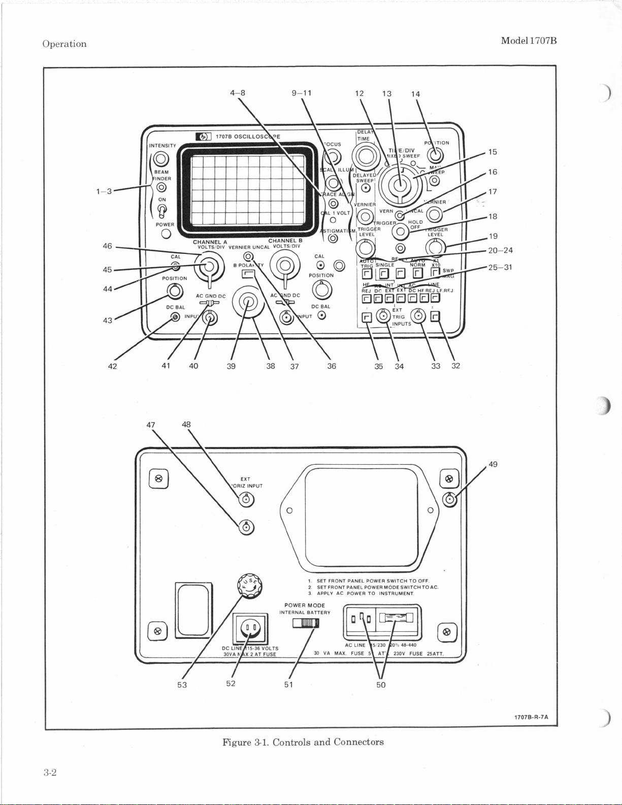
0
b
F
P
OPERATING AND
SERVICE
MANUAL
OSCILLOSCOPE
1707B
HEWLETT
~-
-
_-
-
PACKARD
Page 2

.
OPERATING AND SERVICE MANUAL
MODEL
1707B
OSCILLOSCOPE
4
SERIALS
Refer to Section
standard options:
and
631.
PREFIXED:
VI1
for instruments with the following
002,007,011,012,015,602,607,611
1410A
H
1900
Manual
Microfiche Number 01 707-908 16
Part
Number 01707-90916
EWLETT-PAC KA R D
GARDEN
OF
THE GODS ROAD, COLORADO SPRINGS, COLORADO, U.S.A.
COMPANY/COLO RA DO SPRINGS DIV
IS1
ON
PRINTED: APRIL
1974
Page 3
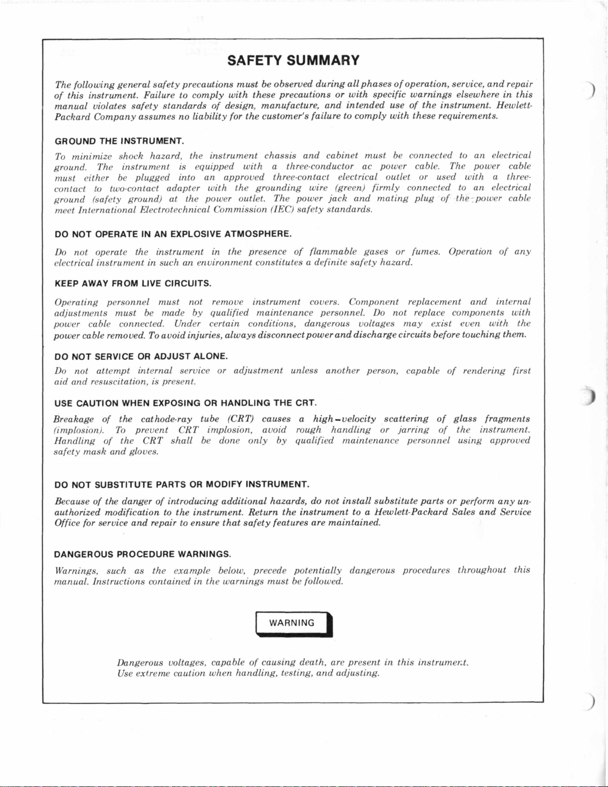
SAFETY
SUMMARY
The following general safety precautions must be observed during all phases of operation, service, and repair
of this instrument. Failure to comply with these precautions
or
with specific warnings elsewhere
in
this
manual violates safety standards of design, manufacture, and intended use of the instrument. HewlettPackard Company assumes no liability for the customer's failure to comply with these requirements.
GROUND THE INSTRUMENT.
To minimize shock hazard, the instrument chassis and cabinet must be connected to an electrical
ground. The instrument is equipped with a three-conductor ac power cable. The power cable
must either be plugged into an approved three-contact electrical outlet
or
used with a three-
contact to two-contact adapter with the grounding wire (green) firmly connected to an elmtrical
ground (safety ground) at the power outlet. The power jack and mating plug of the-power cable
meet International Electrotechnical Commission
DO NOT OPERATE IN AN EXPLOSIVE ATMOSPHERE.
Do
not operate the instrument
in
the presence of flammable gases
(IEC)
safety standards.
or
fumes. Operation of any
electrical instrument in such an environment constitutes a definite safety hazard.
KEEP
AWAY
FROM LIVE CIRCUITS.
Operating personnel must not remove instrument covers. Component replacement and internal
adjustments must be made by qualified maintenance personnel.
Do
not replace components with
power ca ble connected. Under certain conditions, dangerous voltages may exist even with the
power cable removed.
To
avoid injuries, always disconnect power and discharge circuits before touching them.
DO NOT SERVICE
Do
not attempt internal service
OR
ADJUST ALONE.
or
adjustment unless another person, capable of rendering first
aid and resuscitation, is present.
USE CAUTION WHEN EXPOSING
Breakage of
the
cathode-ray tube (CRT) causes a high-velocity scattering of glass fragments
(implosion). To prevent
Handling of the
CRT
shall be done only by qualified maintenance personnel using approved
OR
HANDLING THE CRT.
CRT
implosion, avoid rough handling or jarring of the instrument.
safety mask and gloves.
DO NOT SUBSTITUTE PARTS
Because of
the
danger of introducing additional hazards,
OR
MODIFY INSTRUMENT.
do
not install substitute parts
or
perform any
un-
authorized modification to the instrument. Return the instrument to a Hewlett-Packard Sales and Service
Office for service and repair to ensure that safety features are maintained.
DANGEROUS PROCEDURE WARNINGS.
Warnings, such as the example below, precede potentially dangerous procedures throughout this
manual. Instructions contained in the warnings must be followed.
I
Dangerous voltages, capable of causing death, are present in this instrumezt.
Use
extreme
caution when handling, testing, and adjusting.
Page 4

Model
1707H
TABLE
Section Page
I
GENERAL INFORMATION
1.1
1.4
1.5
1.7
1-1
1.17
1.20 .
1.22 .
1.24 .
1.26 .
1.30 .
I1 INSTALLATION .........................
2.1
2.3 .
2.6 .
2.7
2-1
2.13
2- 15 .
2.17 .
2.19 .
I11 OPERATION
3.1
3.3
3.5
3.7
3.9
3.11
3.13
3.15
3.17
3.24
3.26
3.28
3.30
3.32
3.34
3.36
3.38
3.40
J
I
I
3.42 .
3.44
3.46 .
Introduction
.
.
Description
.
.
1
.
.
.
.
1
.
.
.
.
.
.
.
.
.
.
.
.
. B
.
.
.
.
.
.
.
.
Introduction
Vertical Circuits
Horizontal Circuits
Cathode-ray Tube
Warranty
Accessories Furnished
Accessories Available
Instrument and Manual
Identification
Inquiries
Introduction
Initial Inspection
Preparation for Use
Power Requirements
Three-conductor AC Power
Cable
DC
Battery Installation
Claims
Repacking for Shipment
Introduction
Controls and Connectors
Beam Finder
Scale Illumination
Trace Align
Calibrator
Focus and Astigmatism
Coupling
Display
Trig
Polarity
Sweep Display
Ext
Main Sweep
Mixed Sweep
Delayed Sweep
Time/Div
Vernier
Trigger Level
Trigger Holdoff
Slope
......................
.......................
......................... 1-5
..........................
...................... 2-1
.......................
Plug
......................
............................
.............................
......................
...................... 3-1
........................
.........................
............................
...................... 3-4
Horiz Input
....................... 3-4
.........................
............................ 3.4
..............
..................
..............
............
.................
............ 1-5
.............
................... 1-5
.................
............... 2-1
..........
...........
.......... 2-2
..........
....................
.............. 3-1
.....................
.........
..................
................. 3-4
.................... 3-4
...................
.................. 3-4
...................
.................
1-1
1-1
1 . 1
1-1
1-1
1-1
1-5
1-5
1-5
2-1
2-1
2-1
2-1
2-2
2-2
2-2
3-1
3-1
3-1
3-1
3-1
3-1
3-1
3-4
3-4
3-4
3-4
3-4
3-4
3-4
OF
CONTENTS
Section Page
IV PRINC11’1,ES OF OPERATION
3.48 .
3.51 .
3.54 .
3.56 .
3.58
.
3.59
.
3.61
.
3.63
.
3.65 .
3.67
.
3.69 .
3.71 .
3.73
.
3.75 .
3.77 .
3.80 .
4.1
.
4.3
.
4.6 .
4.8
.
4-
10
.
4-12
4.14
.
4-
16
.
4.21 .
4.24 .
4.27
.
4..31
.
‘1
-;
35
.
4.41
.
4.44
.
4.46
.
4.48
.
4.53 .
4.79
.
4.81
.
4.86
.
4.104 .
4-1 19 .
4.124
4- 130
4.148 .
4.156 .
4.158 .
4.162
4.165 .
4.174 .
Sweep Mode
Trigger Selection
Magnetic Interference
Battery Recharge Operation
Preoperational Adjustments
Initial Turn.on
Focus and Astigmatism Adjust
Operating Procedures
Operators Performance Check
Operating Information
Auto Versus
Auto Versus
AC Versus DC
Mixed Sweep
Delayed Sweep
Line Sync
Introduction ......................
Block Diagram Discussion
Input Attenuator
Vertical I’rcamplifier
1)cllay
Vertical Output Amplifier
Trigger Circuits
M
ai n In t egr a t o r
Holdoff and Comparator
I
)el ay ed Integra tor
‘l’iming Sequence
Horizontal Mode Assembly
I.
ow
Voltage Power
High Voltage Power Supply
Gate Amplifitr
Detailed Circuit Theory
Input Attenuators
Vertical Preamplifier
Delay Line
Vertical Output Amplifier
Trigger Circuits
Main Integrator
Holdoff and Comparator
.
Delayed Integrator
.
Horizontal Mode
Gate Assembly
Calibrator
Horizontal Preamplifier and
Output Assemblies
Indicator Drivers
.
Low Voltage Power
Supply
High Voltage Power
Supply
....................
................
............. 3-5
..................
.............
............
Norm
..............
Trig
...............
.................. 3-7
....................
..................
....................... 3-7
...........
..............
I.ine
....................
...............
...............
............
..............
Supply
................
..........
.............. 4-4
...........
.....................
................
................
............ 4-10
..............
.................
.....................
...........
..............
.......................
.......................
....... 3-5
.......
.. 3-6
..... 3-6
.......
..........
.....
......
....
....
...
...... 4-6
......
3-5
3-5
3-5
3-5
3-6
3-7
3-7
3-7
3-7
3-7
4-1
4-1
4-1
4-1
4-1
4-1
4-1
4-1
4
.
4-2
4-2
4-;3
4-:3
4-;j
4-3
4-4
4-4
4-4
4-6
4-6
4-8
4-10
4-11
4-13
4-14
4-14
4-14
4-14
4-16
1
111
Page 5

Table of Contents
Model 1707B
TABLE
Section Page
V
PERFORMANCE: CHECK AND
A1)JUS’I’ME:NTS
5.1
5.3
5.5
5.8
5.10
5-
5.13
5.18
5.23
5.28
5.33
5.38
5.43
5.48
5.53
5.58
5.63
5.68
5.73
5-78
5.83
5.88
5.93
5.98
5.103
5.108
5-113
5.118
5.123
5.128
5-133
5.138
5.142
5.143
5.148
5.153
5.157
5.162
5.167
5.172
5.177
5.181
5-
Introduction
.
Test Equipment
.
Performance Check
.
Front-panel Adjustments
.
Front-panel Settings
.
Performance Tests
12
.
Deflection Factor
Rise time
Handwidth
A+B Mode
Alt Mode
Chop Mode
Single Sweep
Auto
Z
Axis
Beam Finder
Coupling Switch
Input Resistance
Common Rejection Ratio
(CMRR)
Main
Delayed Sweep Time
Delay Time Accuracy
Delay Time Linearity
Delay Jitter
Main Triggering
Delayed Triggering
Main Trigger Level Range and
Polarity
Delayed Trigger Level Range
and Polarity
Ext Horizontal Bandwidth
Ext Horizontal Deflection
Factor
Calibrator
Adjustments
Adjust Procedures
Low
Adjustment
High
Adjustment
Intensity Limit Adjustment
Y-Axis
Gate Amplifier Response
Adjustment
Trigger Amplifier Balance and
DC
Trigger Sensitivity
Position Centering Adjustment . 5-22
Sweep Length Adjustment
Main Sweep Timing
Adjustment
185
.
.
.
.
.
.
.
.
.
.
.
.
.
.
.
.
.
.
.
.
.
.
.
.
.
.
.
.
.
.
.
.
.
.
.
.
.
.......................
......................
...................
...............
..........
..............
................
.............
.....................
....................
......................
.......................
.....................
...................
Trig
Recovery Time
Sensitivity
...............
....................
................
................
......................
Sweep Time
...............
............
..........
..........
....................
...............
............
......................
.................
......................
.....................
.....................
................
Voltage Power Supply
..................
Voltage Power Supply
..................
Alignment
..............
..................
Adjustment
.............
.............
..................
OF
........
....
....
.....
CONTENTS
5-1
5-1
5-1
5-1
5-
5-1
5-1
5-1
5-2
5-3
5-3
5-4
5-4
55
5-5
56
5-6
5-6
5-7
5-8
5-8
5-9
5-10
511
5-12
5-13
5-14
5-15
5-16
5-16
5-17
5-17
5-19
5-19
5-19
5-19
5-20
520
5-20
5-21
5-21
5-22
523
(Cont’d)
Section Page
5.190
5.195
5.200
5.205
5.210
5-2
1
VI REPI.ACEAH1. E PARTS
VI1
VI11 SCHEMATICS ANI) TROUH1.E:
15
5.220
5.225
5.230
6.1
.
6.3
.
MAZNUAI. CHANGES AN!)
7.1
.
7.3
.
7.5
.
7.9
.
SHOOTING
8.1
.
8.3
.
8.8
.
8-
12
8-
1.5
8-
17
8.22
8.27
8.29
8-:3
1
8..n
8..35 .
8437
8.42
8.44
.
8.46
.
8.48
.
Delayed Sweep Time
.
.
.
.
.
.
.
.
.
.
.
.
.
.
.
.
.
.
.
Adjustment
X10 Gain Adjustment
Mag Centering Adjustment
Calibrator Adjustment
Ext Horiz Input Compensation . 5-25
Ext
Horiz
Low-frequency Pulse Response
Adj
............................
Input Capacitance and Attenuator
Compensation Adjustment
High-frequency Pulse
Response Adj
Introduction
Ordering Information
Introduction
Manual Changes
Special Options
Standard Options
............................
Introduction
Schematics
Reference Designations
Component
Preventive Maintenance
Mechanical Inspection
Switch Maintenance
Repair and Replacement
CRT Removal and Replace-
ment
Vertical Amplifier Module
Removal and Replacement
Delay line Removal and
Replacement
Attenuator Removal
Replacement
Removal and Replacement
Assemblies in Horizontal
Amplifier Module
Power
Removal and Replacement
Power
assembly and Reassembly
Semiconductor Removal and
Replacement
At
t
e
n
u
..................
Gain Adjust
...............
.................
......................
.............
OP‘I’IONS
......................
..................
...................
.................
......................
.......................
...........
I.
ocations
........................
S
u
p p
1
Supply
a
t o r Ser vi c i n
.............
................ 8-3
................
...........
y
Mod
u
1
e
Module
................
g
..........
....
.........
.........
. .
....
.
..........
........
..........
..........
. . 8-3
and
of
IXs-
. .
..........
5-23
524
524
5-25
5-26
5.26
5-26
5-27
6-1
6-1
6-1
7-1
7-1
7-1
7-1
7-1
8-1
8-1
8-1
8-1
8-1
8-1
8-1
8-2
8-2
8-2
8-3
8-5
8-5
8-5
8-6
8-6
iv
Page 6

Model 1707B
Table of Contents
List of Illustrations
TABLE
)
Section Page Section Page
8.50 . Circuit Hoards
8.52
.
8.54
.
8.56
.
8.60
.
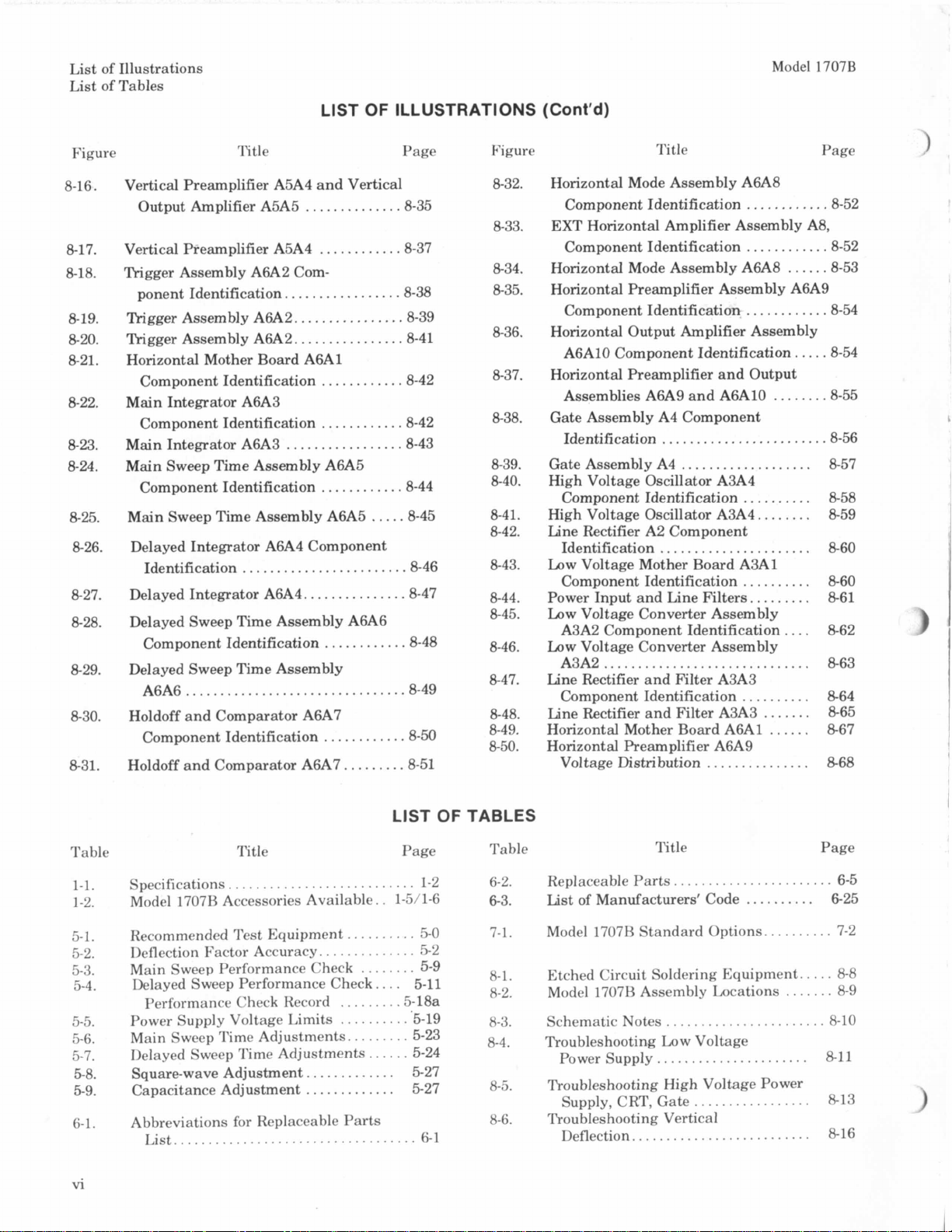
Figure Title Page Figure Title Page
.
1.1 Model 1707R Oscilloscope 1-0 5.12
1.2
.
Instrument Serial Number
1.3
2.1
2.2 Battery Pack Installation 2-2 5-16 . EXT Horizontal Bandwidth
3.1
3.2
1
3.3
3.4
3.5
3.6
3.7
4.1
4.2
4.3
4.4
5.1
5-2
5.3
5-4
55
5-6
5-7
58
59
5-10
5-11
Service Kit for HP 1700-series
.
Oscilloscopes
.
Rear Panel Power Module
.
.
Controls and Connectors 3-2
Sweep Combinations
.
.
DC BAL Adjust
.
CALAdjust
Algebraic Addition and Differential
.
Operation
Delayed Sweep
.
Mixed Sweep
.
Timing Sequence
.
Step-by-step operation of the
.
.
.
.
.
.
.
.
.
.
.
.
Gate Schmitt Trigger
Step-by-step operation of the Set-
reset Multivibrator 4-9
Blanking Sequence
Deflection Factor Test Setup
Rise time Test Setup
Bandwidth Test Setup
A+B
Input Resistance Test Setup
CMRR Test Setup
Main Sweep Time Test Setup
Delayed Sweep Time Test Setup
Delay Time Accuracy Test Setup
.
Delay Time Linearity Test Setup
Delay Jitter Test Setup
.
Hoard Connect ions
Servicing Etched Circuit
Hoards
Integrated Circuit Replace- 8-7 1
ment 8.6 8.73
Service Kit
.............................
............................
...........................
Mode Test Setup
.....................
.............
.......................
.........................
.....................
...............
............
.......................
...............
...............
................
....................
.........................
.........................
........................
...............
..................
...................
............
....................
.................
..................
.............
.......................
............
.................
OF
LIST
OF
........
.......
.......
CONTENTS (Cont'd)
8-6
8-6
8.6
8.7
8.62
.
8.64
.
8.66 . Troubleshooting
8.69
.
.
.
8.75
.
Soldering
Aids
.........................
Heat Sink Removal
DC Voltages
Waveforms
Test Points
Circuit Checking
ILLUSTRATIONS
.
Main Triggering
5.13
.
1-5
1-6
2-1 Polarity Test Setup
3-5
3-8 Test Setup
3-9
3-10
3-11
3-12
4-2
4-7
4-12
5-2
5-3
33
5-4
5-7
5-8
5-8
5.10
5.10
5.11
5.12
5.14
5.15
517
518
5-19
6-1
6-2
8.1
8.2
8.3
8.4
8.5
8.6
8.7
8-8
8-9
8-10
8.11
8.12
8.13
8-14
8-15
Delayed Triggering Test Setup
Main Trigger Level Range and Polarity
.
Test Setup
.
Delayed Trigger Level Range and
Test Setup
EXT
.
Horizontal Deflection Factor
...........................
...........................
...........................
.
Calibrator Test Setup
Adjustment
.
Knob Locator
.
Mechanical
.
Vertical Module Mechanical Parts
.
.
.
.
.
.
.
.
.
Removal
Attenuator Removal
Semiconductor Terminal Identification
Component Identification. Interior Front
and rear Panel
Component and Assembly Locations . 8-23
Vertical Module A5 Component
Identification
Horizontal Module A6 Component
Identification
Main Block Diagram
Power Supply Block Diagram
Attenuator Component Identification . 8-28
.
Attenuator Schematic
.
Vertical Preamplifier Assembly A5A4
.
Component Identification
Vertical Preamplifier Assembly
.
A5A4
Vertical Preamplifier Assembly
.
A5A4
.
Vertical Preamplifier Assembly A5A4
Component Identification
..........................
...........................
Parts
..............................
......................
......................
..............................
................................
Tool.
Solder. and
............
...................
...................
....................
....................
...............
Test
Setup
............
.........
................
..................
Locator
.....................
...............
....................
.................
........
................
..........
............
8-7
8.8
8.8
8.8
8.8
8.8
8.9
5.13
5.14
5.15
5-16
5.17
5.17
5.18
529
6-2
6-3
8-4
8-4
. .
8-7
8-23
8-24
8-24
8-25
8-27
8-29
830
8-31
8.33
8.34
V
Page 7
List of Illustrations
List
of
Tables
LIST
OF
ILLUSTRATIONS
(Cont‘d)
Model
1707B
Figure Title Page
8.16
8.17
8.18
8.19
8.20
8-21
8.22
8.23
8.24
8.25
8.26
8.27
8-28
8.29
8.30
8.31
Vertical Preamplifier A5A4 and Vertical
.
Output Amplifier A5A5
Vertical Preamplifier A5A4
.
Trigger Assembly A6A2 Com-
.
ponent Identification
Trigger Assembly A6A2
.
Trigger Assembly A6A2
.
.
Horizontal Mother Board A6A1
Component Identification
.
Main Integrator A6A3
Component Identification
Main Integrator A6A3
.
.
Main Sweep Time Assembly A6A5
Component Identification
Main Sweep Time Assembly A6A5
.
Delayed Integrator A6A4 Component
.
Identification
Delayed Integrator A6A4
.
Delayed Sweep Time Assembly A6A6
.
Component Identification
Delayed Sweep Time Assembly
.
A6A6
................................
Holdoff and Comparator A6A7
.
Component Identification
.
Holdoff and Comparator A6A7
........................
..............
............
.................
................
................
............
............
.................
............
...............
............
............
.....
.........
8.35
8.37
8.38
8.39
8.41
8-42
8.42
8.43
8.44
8.45
8.46
8.47
8.48
8-49
8.50
8-51
Figure Title Page
8.32
8.33
8-34
8.35
8-36
8.37
8.38
8.39
8.40
8.41
8.42
8.43
8.44
8.45
8.46
8.47
8.48
8.49
8.50
Horizontal Mode Assembly A6A8
.
Component Identification
EXT Horizontal Amplifier Assembly A8.
.
Component Identification
Horizontal Mode Assembly A6A8
.
Horizontal Preamplifier Assembly A6A9
.
Component Identification
Horizontal Output Amplifier Assembly
.
A6A10 Component Identification
Horizontal Preamplifier and Output
.
Assemblies A6A9 and A6A10
Gate Assembly A4 Component
.
Identification
Gate Assembly A4
.
High Voltage Oscillator A3A4
.
Component Identification
High Voltage Oscillator A3A4
.
.
Line Rectifier A2 Component
Identification
Low Voltage Mother Board A3A1
.
Component Identification
.
Power Input and Line Filters
.
Low Voltage Converter Assembly
A3A2 Component Identification
.
Low Voltage Converter Assembly
A3A2
..............................
.
Line Rectifier and Filter A3A3
Component Identification
Line Rectifier and Filter A3A3
.
.
Horizontal Mother Board A6A1
Horizontal Preamplifier A6A9
.
Voltage Distribution
........................
...................
......................
............
............
............
..........
..........
.........
..........
...............
......
.....
........
........
....
.......
......
8.52
8.52
8.53
8.54
8.54
8.55
8.56
a57
8-58
8-59
a60
8-60
8-61
a62
8-63
864
a65
8-67
868
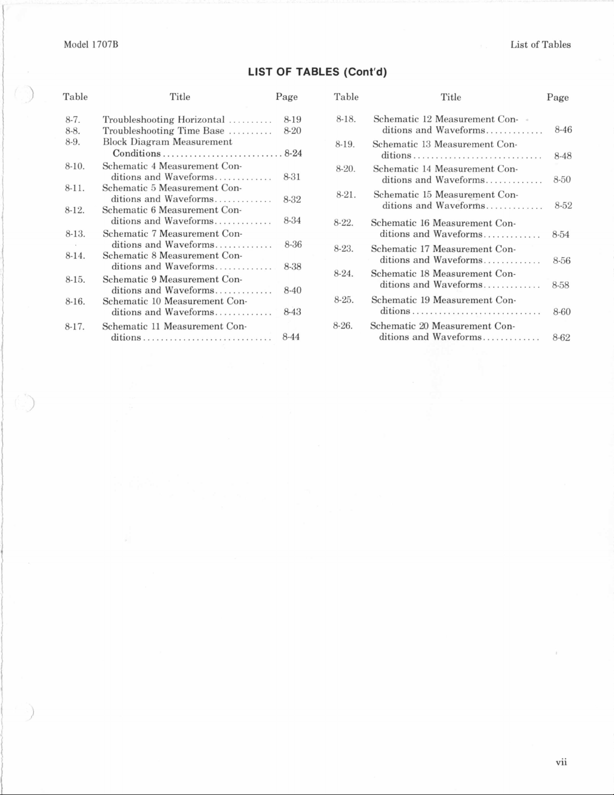
Table
1.1
.
1.2
.
5.1
.
5.2
.
5.3
.
5.4
.
5.5
.
5.6
.
5.7
.
5.8
.
5.9
.
6.1
.
vi
LIST
OF
TABLES
Title Page Table
Specifications
Model 1707H Accessories Available
Recommended Test Equipment
Ileflection Factor Accuracy
Main Sweep Performance Check
Delayed Sweep Performance Check
Performance Check Record
Power Supply Voltage Limits
Main Sweep Time Adjustments 5-23 8.4
Ilelayed Sweep Time Adjustments
Square-wave Adjustment
Capacitance Adjustment
Abbreviations for Replaceable Parts
List
...................................
...........................
. .
1-5/14? 6.3
..........
..............
........
....
.........
..........
.........
......
.............
.............
1-2
5-0
5-2
5-9
5-11
5.18a
‘5-19
5-24
5-27
5-27
6-1
6.2
8.1
8.3
8.5
7.1
8.2
8.6
Title Page
Replaceable Parts
.
List of Manufacturers’ Code
.
Model 1707H Standard Options
.
Etched Circuit Soldering Equipment
.
Model 1707H Assembly Locations
.
Schematic Notes
.
.
Troubleshooting Low Voltage
Power Supply
.
Troubleshooting High Voltage Power
Supply.
Troubleshooting Vertical
.
Deflection
CRT.
.......................
.......................
......................
Gate
.................
..........................
..........
..........
.....
.......
6-5
6-25
7-2
8-8
8-9
8-10
8-11
8-13
8-16
Page 8
Model
1707B
LIST
OF
TABLES
List of Tables
(Cont’d)
Table
8-7.
8-8.
8-9.
8-
10.
8-1 1.
8-
12.
8-13.
8-14.
8-15.
8-16.
8-17.
Title Page Table Title Page
Troubles hooting Horizontal
Troubleshooting Time Base
Block Diagram Measurement
Conditions
Schematic 4 Measurement Con-
ditions and Waveforms..
Schematic 5 Measurement Con-
ditions and Waveforms..
Schematic 6 Measurement Con-
ditions and Waveforms..
Schematic 7 Measurement Con-
ditions and Waveforms.. 8-36
Schematic 8 Measurement Con-
ditions and Waveforms..
Schematic 9 Measurement Con-
ditions and Waveforms..
Schematic 10 Measurement Con- 8-25. Schematic 19 Measurement Con-
ditions and Waveforms..
Schematic
ditions..
..........................
11
Measurement Con- 8-26. Schematic 20 Measurement Con-
...........................
..........
..........
...........
...........
...........
...........
...........
...........
...........
8-
19
8-20
.8-24
8-31
8-32
83-34
8-38
8-40
843 ditions..
8-44 ditions and Waveforms..
8-18.
8-19. Schematic
8-20. Schematic
8-21. Schematic
8-22. Schematic 16 Measurement Con-
8-23. Schematic 17 Measurement Con-
8-24. Schematic
Schematic 12 Measurement Con-
ditions and Waveforms..
13
Measurement Con-
ditions..
ditions and Waveforms..
ditions and Waveforms.
ditions and Waveforms..
ditions and Waveforms.
ditions and Waveforms.
...........................
14
Measurement Con-
15
Measurement Con-
18
Measurement Con-
...........
...........
............
...........
............
............
...........................
...........
8-46
8-48
8-50
8-52
8-54
8-56
8-58
8-60
8-62
vii
i
Page 9
Gcncral Information
Model 1707B
1-0
<.*
-"
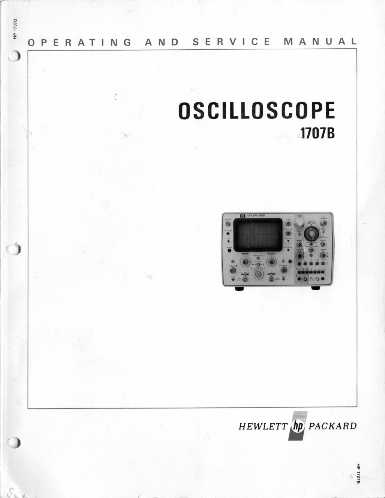
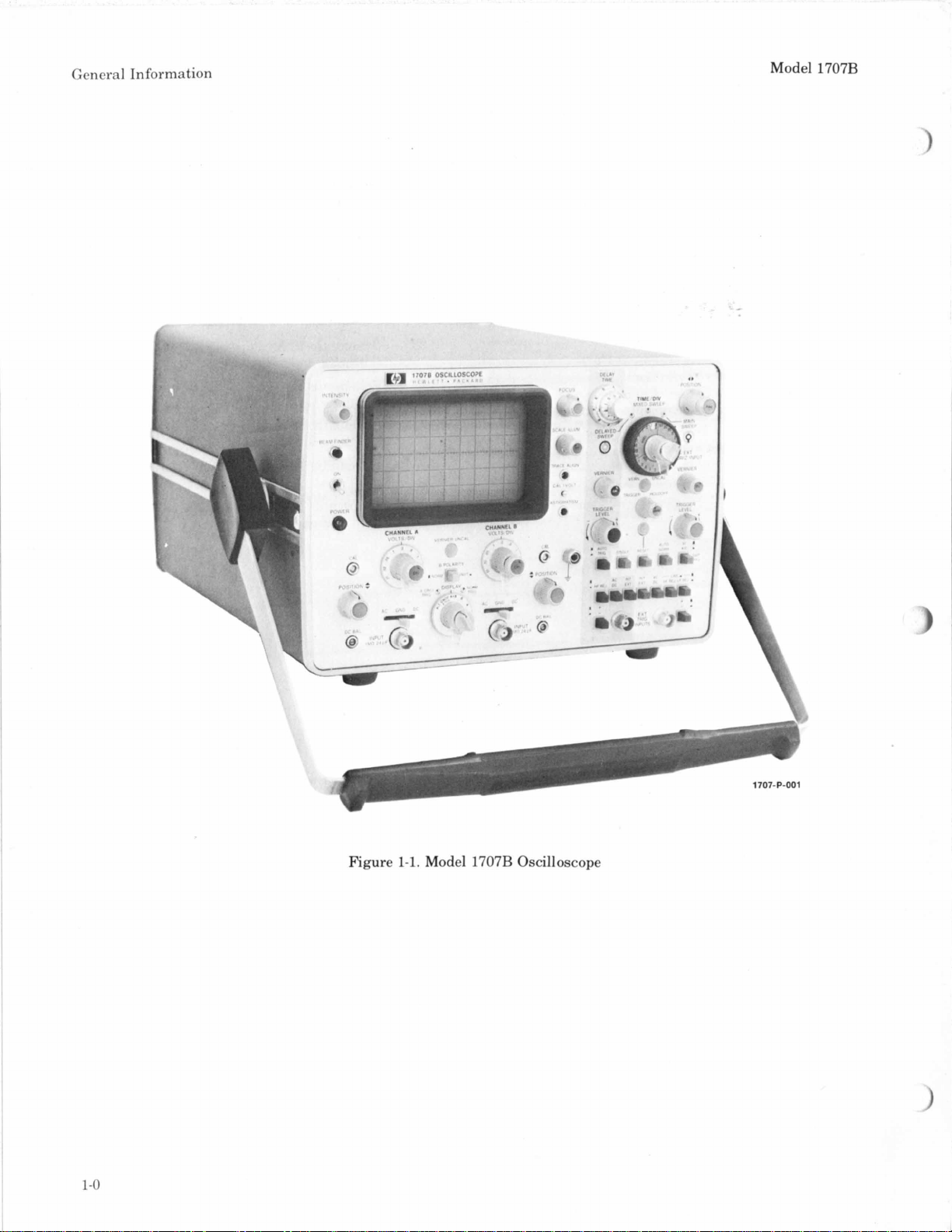
Figure
1-1.
Model 1707B Oscilloscope
1707-PO01
Page 10
Model 1707B
1
I
h
General Information
SECTION
I
GENERAL INFORMATION
1-1.
INTRODUCTION.
1-2.
This
manual provides operating and service
information for the Hewlett-Packard Model 1707B
i
Oscilloscope (figure
1-1).
This manual
is
divided into
eight sections, each covering a specific topic or
aspect of the instrument. All schematics are located
at
the rear of the manual.
the manual are instruction cards located
Also
located
at
the rear of
in
an
envelope attached to the inside back cover. These
cards explain the function of each instrument control.
The card
is
designed to fit the inside lid of the front
panel storage cover.
1-3. This section contains a description of Model
1707B. Instrument specifications are listed in table
1-1.
Table 7-2 lists the options available for Model
1707B.
1-4.
DESCRl PTION.
1-10. With the dual-trace feature, displays can be
obtained on either channel A or B, channels A
and B together, channels A + B, and channels A
-
B. Simultaneous display of two signals
is
possible
in either chop or alternate mode of operation. During
chop operation, channels are switched
at
an approximate rate of 400-kHz during each sweep. In the
alternate mode of operation, the signal applied to
each channel
Triggering
is
displayed on alternate sweeps.
is
selectable from either A ONLY TRIG
or NORM TRIG position. In the NORM TRIG position,
the instrument triggers on the displayed signal.
In the A ONLY TRIG position, the instrument
triggers on the signal applied to channel A.
1-11.
HORIZONTAL CIRCUITS.
1-12. The horizontal circuits provide four types of
sweep displays. The displays are main sweep, mixed
sweep, delayed sweep and external horizontal input.
1-5.
INTRODUCTION.
1-13.
Operation of the delayed sweep while in the
main sweep mode provides trace intensification.
1-6. The Model 1707B
is
a
general-purpose, wideband oscilloscope designed for bench or field service.
The Model 1707B operates from an ac line, dc line
or optional battery pack. The optional ,rechargable
nickel cadmium batteries provide up
to
4% hours of
operation and require a recharge time of approximately
of transportation and
14
hours. A carrying handle provides ease
is
adjustable, allowing the
Model 1707B to be placed at an angle for viewing
the CRT.
i
1-7.
VERTICAL CIRCUITS.
The amount of intensification width depends on the
delayed front panel settings. In the delayed mode,
the intensified portion is displayed across the entire
CRT.
1-14.
Sweep speed settings from 0.1 usec/div to
2 sec/div (main sweep) and 0.1 usec/div to
0.2 sec/div (delayed sweep) are available in
a
1,
2,
sequence. Vernier controls allow continuous adjustment between steps and extend the slowest sweep
to 5 sec/div (main sweep) and
0.5
sec/div (delaved
>I
sweep). Using the magnifier function, the fastest
sweep speed can be expanded to 10 ns/div. The
5
mixed sweep function provides for simultaneous
1-8.
Vertical bandwidth
is
75
MHz with a rise time
less than 4.7 ns. Maximum vertical deflection factor
is
10 mV/div. The Model 1707B contains two identical
vertical amplifiers for single or dual channel
display of an input waveform and an expanded
portion of the waveform.
The delayed circuits are
calibrated, permitting accurate time difference meas-
urements to be made.
operation. Each channel offers a choice of ac or
1-15.
dc coupling. Common mode rejection
dB
at 10 mV/div, and
20
dB
for the rest of the
deflection ranges.
is
at
least .40
The main and delayed trigger circuits have
provisions for either internal or external operation.
Choice of trigger coupling
is
provided; ac/dc,
high
frequency reject, and low frequency reject. The
1-9. Nine calibrated switch settings provide
a
deflection factor range from 10 mV/div to 5 V/div in
a
1, 2, 5 sequence. The vertical verniers permit
continuous adjustment between calibrated steps and
extend the least sensitive deflection factor
div) to
at
least 12.5 V/div.
(5
V/
delayed trigger circuit does not have low frequency
reject trigger coupling.
1-16.
An external horizontal input allows the use of
an external signal to drive the horizontal deflection
plates of the CRT.
1-1
Page 11
General Information Model 1707B
Table
1-1.
Specifications
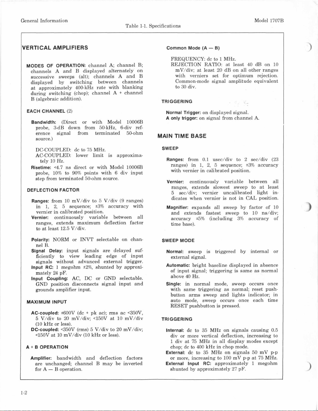
IERTICAL AMPLIFIERS
MODES OF OPERATION:
channels A and B displayed alternately on
successive sweeps (alt); channels
displayed by switching between channels
at approximately 400-kHz rate with blanking
during switching (chop); channel A + channel
B
(algebraic addition).
EACH CHANNEL
Bandwidth:
(2)
(Direct or with Model 10006B
probe, 3-dB down from 50-kHz, 6-div reference signal from terminated 5@ohm
source.)
DC-COUPLED: dc
AC-COUPLED: lower limit
tely
10
Hz.
Risetime:
probe, 10%
<4.7
ns
to
90%
step from terminated 50-ohm source.
DEFLECTION FACTOR
Ranges:
from 10 mV/div to 5 V/div
in 1,
2,
5
sequence;
vernier in calibrated position.
Vernier:
continuously variable between all
ranges, extends maximum deflection factor
to
at
least 12.5 V/div.
channel A; channel B;
A
to
75 MHz.
is
approxima-
direct or
with
Model 10006B
points with 6 div input
*3%
accuracy with
(9
and B
ranges)
Common Mode (A
-
B)
FREQUENCY: dc to 1 MHz.
REJECTION RATIO:
mV/div;
at
least
at
least
40
20
dB on all other ranges
with verniers set for optimum rejection.
Common-mode signal amplitude equivalent
to 30 div.
TR
I
G GE
RI
N
G
Normal Trigger:
A only trigger:
on displayed signal.
on signal from channel A.
MAIN TIME BASE
SWEEP
Ranges:
ranges) in 1,
with vernier
Vernier:
ranges, extends slowest sweep to
5
dicates when vernier
Magnifier:
and extends fastest sweep to 10 ns/div;
accuracy *5% (including
time base).
from 0.1 usec/div to 2 sec/div (23
2,
5
sequence; *3% accuracy
in
calibrated position.
continuously variable between all
sec/div; vernier uncalibrated light
is
not in
CAL
expands all sweep by factor of 10
3%
accuracy of
dB
on 10
at
least
position.
in-
Polarity:
NORM or INVT selectable on chan-
nel B.
Signal Delay:
ficiently
input signals are delayed
to
view leading edge of input
signals without advanced external trigger.
Input
RC
1
megohm
mately
Input Coupling:
24
pF.
*2%,
shunted by approxi-
AC, DC or GND selectable.
GND position disconnects signal input and
grounds amplifier input.
MAXIMUM INPUT
AC-coupled:
5
V/div
*600V (dc + pk ac);
to
20 mV/div; <150V
rms
ac <350V,
at
10 mV/div
(10 kHz or less).
DC-coupled:
<150V
A + B OPERATION
Amplifier:
<350V (rms) 5 V/div to
at
10 mV/div (10 kHz or less).
20
bandwidth and deflection factors
are unchanged; channel B may be inverted
for A - B operation.
suf-
mV/div;
SWEEP MODE
Normal:
sweep
is
triggered by internal or
external signal.
Automatic:
of input signal; triggering
bright baseline displayed in absence
is
same
as
above 40 Hz.
Single:
in
normal mode, sweep occurs once
with same triggering
button
arms sweep and lights indicator; in
as
normal; reset push-
auto mode, sweep occurs once each time
RESET pushbutton
TRIGGER1 NG
Internal:
dc to
is
pressed.
35
MHz on signals causing 0.5
div or more vertical deflection, increasing to
1
div
at
75 MHz in all display modes except
chop; dc
External:
to
400 kHz in chop mode.
dc
to
35
MHz on signals 50 mV p-p
or more, increasing to 100 mV p-p at 75 MHz.
External Input RC:
approximately 1 megohm
shunted by approximately 27 pF.
normal
1-2
Page 12
Model
1707B
Table
1-1.
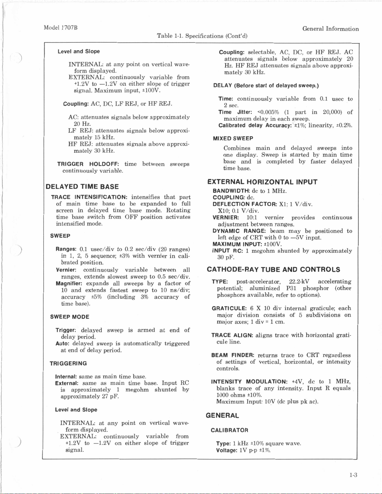
Specifications (Cont’d)
General Information
Level and Slope
INTERNAL
at
any point on vertical wave-
form displayed.
EXTERNAL continuously variable from
+12V
to
-1.2V on either slope of trigger
signal. Maximum input, *lOOV.
Coupling:
AC, DC, LF REJ, or HF REJ.
AC: attenuates signals below approximately
20 Hz.
LF REJ: attenuates signals below approxi-
mately 15 kHz.
HF REJ: attenuates signals above approxi-
mately 30 kHz.
TRIGGER HOLDOFF:
time between sweeps
continuously variable.
DELAYED TIME BASE
TRACE INTENSIFICATION:
of main time base to be expanded to full
screen in delayed time base mode. Rotating
time base switch from OFF position activates
intensified mode.
SWEEP
Ranges:
in 1,
0.1 usec/div to
2,
5
sequence;
brated position.
Vernier:
continuously variable between all
ranges, extends slowest sweep to 0.5 sec/div.
Magnifier:
expands all sweeps by a factor of
10 and extends fastest sweep to 10 ns/div;
accuracy *5% (including
time base).
SWEEP MODE
Trigger:
delayed sweep
delay period.
Auto:
delayed sweep
at end of delay period.
TRIGGERING
same
as
Internal:
External:
is
same
approximately
approximately
Level and Slope
INTERNAL
main time base.
as
main time base. Input RC
27
pF.
at
any point on vertical wave
form displayed.
EXTERNAL continuously variable from
+1.2V
to
-1.2V on either slope of trigger
signal.
intensifies
0.2
sec/div
*3%
with vernier
3%
is
armed
is
automatically triggered
1
megohm shunted by
that
(20
accuracy of
at
part
ranges)
in
cali-
end of
Coupling:
selectable, AC, DC, or HF REJ. AC
attenuates signals below approximately
Hz. HF REJ attenuates signals above approxi-
mately 30 kHz.
DELAY (Before start of delayed sweep.)
Time:
continuously variable from
2
sec.
Time Jitter:
maximum delay
Calibrated delay Accuracy:
MIXED SWEEP
<0.005%
in
each sweep.
(1
part
fl%;
0.1
in
20,000)
linearity,
usec to
Combines main and delayed sweeps into
one display. Sweep
base and
is
is
started by main time
completed by faster delayed
time base.
EXTERNAL HORIZONTAL INPUT
BANDWIDTH:
COUPLl NG:
DEFLECTION FACTOR:
X10;
0.1
VERNIER:
adjustment between ranges.
DYNAMIC RANGE:
left edge of CRT with 0 to -5V input.
MAXIMUM INPUT
INPUT RC:
30
pF.
dc
to
1
MHz.
dc.
X1; 1 V/div.
V/div.
1O:l
vernier provides continuous
beam may be positioned to
*lOOV.
1
megohm shunted by approximately
CATHODE-RAY TUBE AND CONTROLS
TYPE:
potential; aluminized
phosphors available, refer to options).
GRATICULE:
major division consists of 5 subdivisions on
major axes; 1 div
TRACE ALIGN:
cule line.
BEAM FINDER:
of settings of vertical, horizontal, or intensity
controls.
INTENSITY MODULATION:
blanks trace of any intensity. Input R equals
1000 ohms
Maximum Input: lOV (dc plus pk ac).
post-accelerator, 22.2-kV accelerating
P31
phosphor (other
6
X 10 div internal graticule; each
=
1
cm.
aligns
trace with horizontal
returns trace to CRT regardless
+4V, dc to 1 MHz,
*lo%.
GENERAL
CALI B RAT0
Type:
Voltage:
1
kHz
1V
R
*lo%
pp
square wave.
*l%.
20
of
*O.Wo.
grati-
1-3
Page 13

General Information
Table
1-1.
Specifications (Cont'd)
Model 1707B
c
3
1/8
(79.4)
1
7
TOP
1-
14 3/8(365.1)
MAX PROJECTION (1701A)
15 5/16(388.9)
MAX PROJECTION (1701A)
15 9/16(395.31
20 7/8 (530.2)
15
3/4 (400.1)
-1
-
NOTE:
DIMENSIONS IN INCHES
c
c
7 21/64
(1 86.1)
7
53/64
(198.0)
a-
b--11 15/64(286.1)
I
13 3/8(339.7)
AND
(MILLIMETERS)
-4
POWER REQUIREMENTS
AC Line:
DC Line:
Battery (optional)
OPERATING TIME: up
RECHARGE TIME: 14
LOW BATTERY INDICATOR: power light
RECHARGING: batteries are recharging
115V or 230V *20%, 48 to 440 Hz.
11.5V
to
36V.
to
4.5 hours.
hr
minimum charging
time for a fully discharged battery.
flashes
charged and further operation may damage battery.
whenever POWER MODE switch
switch
POWER switch ON, trickle charge
applied.
to
indicate that batteries are dis-
off,
full charge
is
applied; with
is
set to
is
ID
WEIGHT
Without Panel Cover:
ping, 35 lb (15.9 kg).
With Panel Cover and Accessories:
(12.3 kg); shipping,
With Panel Cover, Accessories, and Battery
net, 35 lb (16 kg); shipping, 46 lb
Pack:
(20.9 kg).
DI MENS1 ONS:
ENVIRONMENT (Oscilloscope operates within
specifications over following ranges):
temperature 0°C to +55"C; humidity, to 95%
relative humidity
ft;
vibration, in three planes for 15 min each
with 0.010-inch excursion,
ACCESSORIES FURNISHED:
Model 10115A; front panel storage cover,
Model 10101B; two Model 10006B probes;
and one ac power cord with right angle plug.
refer to outline drawing.
net, 24 lb
38
lb (17.2 kg).
to
40°C; altitude, to 15,000
(11
kg); ship-
net, 27 lb
10
to 55 Hz.
blue contrast filter,
1-4
Page 14
Model 1707B
1-17. CATHODE-RAY TUBE.
1-18. The Model 1707B uses a post-accelerator CRT
with a nonglare, rectangular faceplate. An internal
graticule
to eliminate parallax errors. The CRT
mately 22 -kV accelerating potential, and 6 vertical
by 10 horizontal divisions. Each division
centimeter.
1-19. A type
CRT. Other types of phosphors are available by
special order. Refer to Section VI1 for further information about optional and special-order modifications.
is
located on the same plane
P31
phosphor
is
used in the standard
as
the display
has
approxi-
is
a
square
General Information
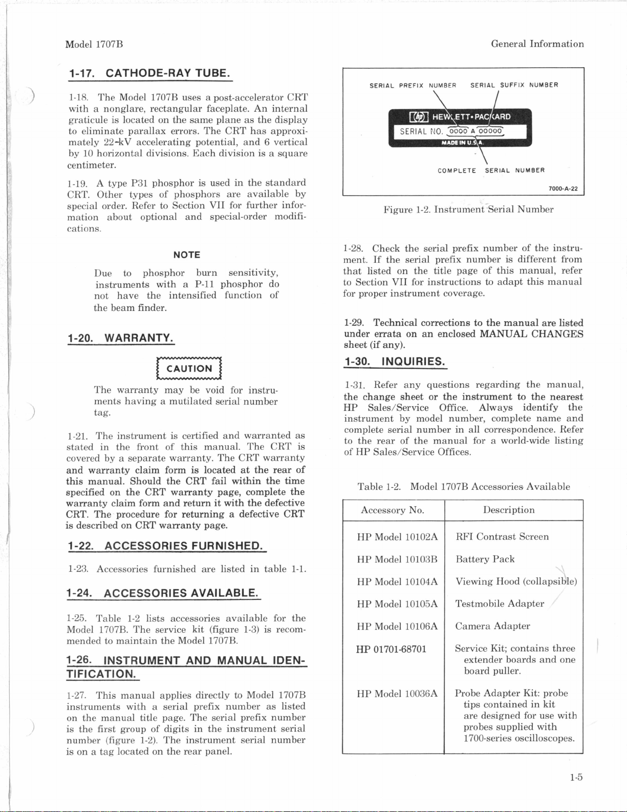
SERIAL PREFIX NUMBER SERIAL SUFFIX NUMBER
rZBirn*h
SERIAL
rJG
0000
A
00000
-\
COMPLETE SERIAL NUMBER
7000-A-22
Figure 1-2. Instrument Serial Number
I
NOTE
Due to phosphor burn sensitivity,
instruments with
not have the intensified function of
the beam finder.
a
P-11
phosphor do
1-20. WARRANTY.
1
CAUTION
The warranty may be void for instruments having a mutilated serial number
tag.
1-21. The instrument is certified and warranted
stated in the front of this manual. The CRT
covered by a separate warranty. The CRT warranty
and warranty claim form
this manual. Should the CRT fail
specified on the CRT warranty page, complete the
warranty claim form and return
CRT. The procedure for returning a defective CRT
is
described on CRT warranty page.
is
3
located
at
the rear of
within
it
with the defective
as
is
the time
1-28. Check the serial prefix number of the instrument. If the serial prefix number
that listed on the title page of this manual, refer
to Section VI1 for instructions
for proper instrument coverage.
1-29. Technical corrections to the manual are listed
under errata on an enclosed MANUAL CHANGES
sheet (if any).
is
different from
to
adapt this manual
1-30. INQUIRIES.
1-31.
Refer any questions regarding the manual,
the change sheet or the instrument to the nearest
HP Sales/Service Office. Always identify the
instrument by model number, complete name and
complete serial number in all correspondence. Refer
to the rear of the manual for a world-wide listing
of HP SaledService Offices.
Table 1-2. Model 1707B Accessories Available
1
Accessory No.
HP Model 10102A
I
Description
RFI Contrast Screen
I
1-22. ACCESSORIES FURNISHED.
I
1-23. Accessories furnished are listed in table
1-1.
HP Model 10103B
HP Model 10104A
Battery Pack
Viewing Hood (collapsible)
1-24. ACCESSORIES AVAILABLE.
Testmobile Adapter
Camera Adapter
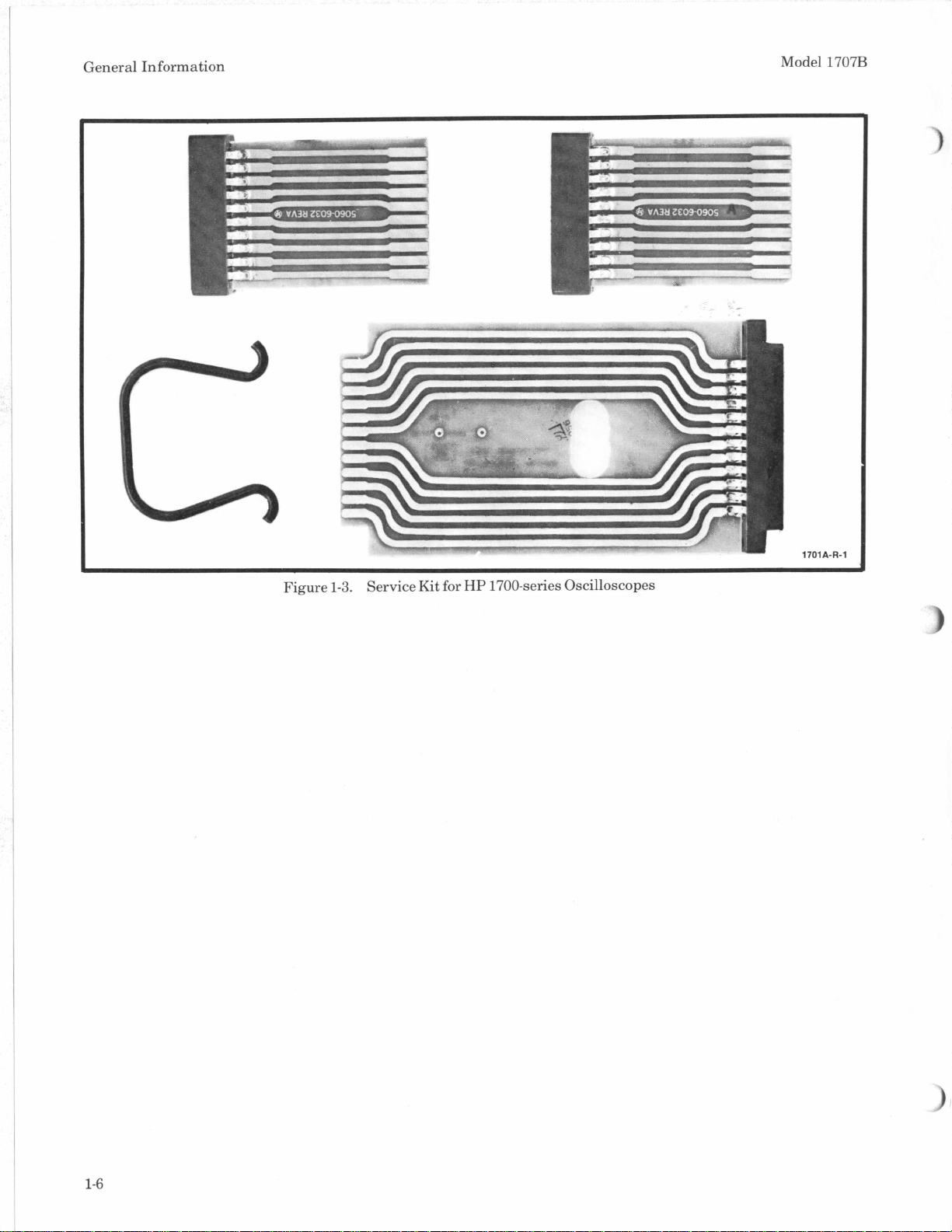
Service Kit; contains three
extender boards and one
board puller.
1-25. Table 1-2 lists accessories available for the
Model 1707B. The service kit (figure
mended to maintain the Model 1707B.
1-3)
is
recom-
1-26. INSTRUMENT AND MANUAL IDEN-
FI
CAT1 ON.
TI
HP Model 10105A
HP Model 10106A
HP
01701-68701
1-27. This manual applies directly to Model 1707B
instruments with a serial prefix number
on the manual title page. The serial prefix number
is
the first group of digits in the instrument serial
number (figure 1-2). The instrument serial number
is
on a tag located on the rear panel.
as
listed
HP Model 10036A
Probe Adapter Kit: probe
tips contained in kit
are designed for use with
probes supplied with
1700-series oscilloscopes.
1-5
Page 15
Gen era1
In
form ation
Model
1707B
Figure
1-3.
Service
Kit
for
HP
1700-series Oscilloscopes
1701A-R-1
I
1-6
Page 16
Model 1707B
Installation
SECTION
I
NSTALLATI 0 N
2-1. INTRODUCTION.
2-2. This section contains instructions for performing an initial inspection of the Model 1707B. Installation procedures and precautions are presented
in step-by-step order. The procedures for making
a
claim for warranty repairs and for repacking the
instrument for shipment are also described
section.
2-3.
INITIAL INSPECTION.
2-4. The instrument was inspected mechanically and
electrically before shipment. Upon receipt, inspect
it
for damage that may have occurred in transit.
Check for broken knobs, bent or broken connectors,
and dents or scratches. If damage
is
to the claims paragraph in this section. Retain the
packing material for possible future use.
in
this
found, refer
II
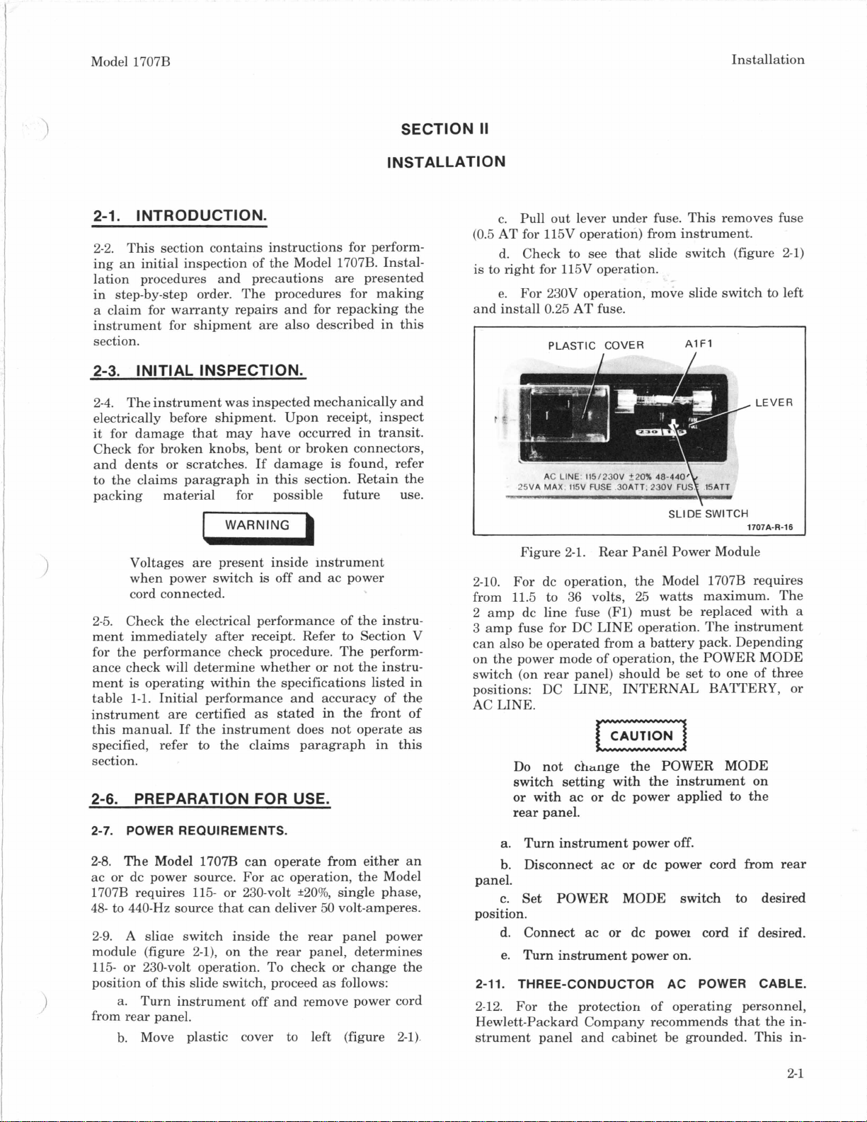
c. Pull out lever under fuse. This removes fuse
(0.5 AT for 115V operation) from instrument.
d. Check to see
is
to right for 115V operation.
e.
For 230V operation, move slide switch to left
and install 0.25 AT fuse.
PLASTIC COVER A1
that
slide switch (figure 2-1)
F1
~
SLIDE
SWITCH
LEVER
1707A-R-16
)
1
Voltages are present inside instrument
when power switch
is
off and ac power
cord connected.
2-5. Check the electrical performance of the instrument immediately after receipt. Refer to Section V
for the performance check procedure. The performance check will determine whether or not the instrument
is
operating within the specifications listed in
table
1-1.
Initial performance and accuracy of the
instrument are certified
this manual. If the instrument does not operate
specified, refer to the claims paragraph
as
stated
in
the front of
in
as
this
section.
2-6.
PREPARATION FOR USE.
2-7.
POWER REQUIREMENTS.
2-8.
The Model
1707B
can operate from either
an
ac or dc power source. For ac operation, the Model
1707B requires
48- to 440-Hz source that can deliver
115-
or 230-volt *20%, single phase,
50
volt-amperes.
2-9. A sliae switch inside the rear panel power
module (figure 2-1), on the rear panel, determines
115- or 230-volt operation. To check or change the
position of this slide switch, proceed
a.
Turn instrument off and remove power cord
as
follows:
from rear panel.
b. Move plastic cover to left (figure 2-1).
Figure 2-1. Rear Pan61 Power Module
2-10. For dc operation, the Model 1707B requires
from
11.5
to 36 volts, 25 watts maximum. The
2 amp dc line fuse
3
amp fuse for DC LINE operation. The instrument
(Fl)
must be replaced with
a
can also be operated from a battery pack. Depending
on the power mode of operation, the POWER MODE
switch (on rear panel) should be set to one of three
positions: DC LINE, INTERNAL BATTERY, or
AC LINE.
Do not change the POWER MODE
switch setting with the instrument on
or
with
ac or dc power applied
to
the
rear panel.
a.
Turn instrument power
b.
Disconnect ac or dc power cord from rear
off.
panel.
c. Set POWER
MODE
switch to desired
position.
d.
Connect ac or dc powei cord if desired.
e. Turn instrument power on.
2-11.
THREE-CONDUCTOR AC POWER CABLE.
2-12. For the protection of operating personnel,
Hewlett-Packard Company recommends that the
strument panel and cabinet be grounded. This
in-
in-
2-1
Page 17
Installation
Model 1707B
strument
is
equipped with a three-conductor ac power
cable that, when connected to an appropriate receptacle, grounds the instrument through the
offset pin. The power jack and mating plug of the
power cord meet International Electro-technical
Commission (IEC) safety standards. To preserve
this
protection feature when operating from a twocontact outlet, use a three-conductor to two-conductor
adapter, and connect the adapter wire to ground
at
the power outlet.
2-13.
2-14. A dc jack
DC
PLUG.
is
provided for operating from a dc
line. The cable used for the dc power cord should
be 2 wire (grounded) and must be able to carry
2.5A of current with a voltage loss of less than
1
volt.
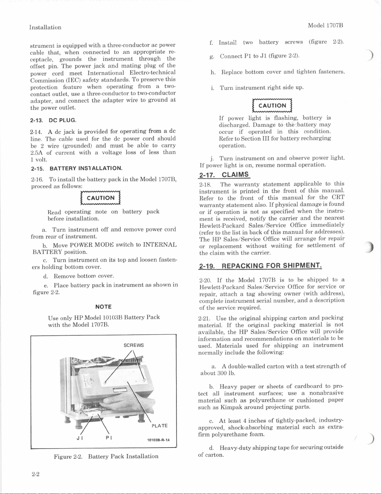
2-15.
BATTERY INSl’ALLATION.
2-16. To install the battery pack in the Model 1707B,
proceed
as
follows:
Read operating note on battery pack
before inst all ation.
a.
Turn instrument off and remove power cord
from rear of instrument.
Move POWER MODE switch
b.
to
INTERNAL
BATTERY position.
Turn instrument on
c.
its
top and loosen fasten-
ers holding bottom cover.
d. Remove bottom cover.
Place battery pack in instrument
e.
as
shown
in
figure 2-2.
NOTE
Use only HP Model 10103B Battery Pack
with the Model 1707B.
SCREWS
f. Instal! two battery screws (figure 2-2).
g.
Connect
P1
to
Jl
(figure 2-2).
h. Replace bottom cover and tighten fasteners.
i.
Turn instrument right side up.
If power light
is
flashing, battery
is
discharged. Damage to the:battery may
occur if operated in this condition.
Refer to Section
I11
for battery recharging
operation.
Turn instrument on and observe power light.
j.
If power light
2-17.
2-18. The warranty statement applicable to
instrument
Refer to the front of
warranty statement also. If physical damage
or if operation
ment
is
is
on, resume normal operation.
CLAIMS
this
is
printed
is
received, notify the carrier and the nearest
not
in
the front
this
as
specified when the instru-
of
this
manual.
manual for the CRT
is
found
Hewlett-Packard Sales/Service Office immediately
(refer to the list in back of this manual for addresses).
The
HP
Sales/Service Office will arrange for repair
or replacement without waiting for settlement of
the claim with the carrier.
2-19.
2-20. If the Model 1707B
REPACKING
FOR
SHIPMENT,
is
to be shipped to
Hewlett-Packard Sales/Service Office for service or
repair, attach a tag showing owner
(with
address),
complete instrument serial number, and a description
of the service required.
2-21. Use the original shipping carton and packing
material. If the original packing material
is
not
available, the HP Sales/Service Office will provide
information and recommendations on materials to be
used. Materials used for shipping
an
instrument
normally include the following:
a
2-2
JI
PI
10103B-R-IA
Figure 2-2. Battery Pack Installation
a.
A double-walled carton with a test strength of
about
300
lb.
Heavy paper or sheets of cardboard to pro-
b.
tect all instrument surfaces; use a nonabrasive
material such
such
as
Kimpak around projecting parts.
as
polyurethane or cushioned paper
c. At least 4 inches of tightly-packed, industry-
approved, shock-absorbing material such
as
extra-
firm polyurethane foam.
d.
Heavy-duty shipping tape for securing outside
of carton.
Page 18
Model 1707B
Operation
SECTION
OPERATION
3-1. I NTR 0 D U CTI ON.
3-2. This section provides general operating instructions and applications information for the Model
1707B. Front-and rear-panel controls and connectors
are identified and briefly described in
figure
Operational adjustments are shown in figures
and 3-4 and general operating instructions are shown
in figures
3-3.
3-5
through 3-7.
CONTROLS AND CONNECTORS.
3-4. The following paragraphs explain some of the
controls and connectors in detail.
3-5. BEAM FINDER.
3-6. Pressing this pushbutton increases intensity
and reduces amplifier gain enough to return beam
to viewing area. This enables the operator to locate
beam and determine the action necessary to center
a
display (examples: reduce input signal amplitude,
change coupling, adjust deflection factor, trigger
level, dc balance, position controls, or intensity).
When centered properly, the beam remains on the
CRT when the pushbutton
is
NOTE
released.
3-1.
3-3
111
3-1 1. CALIBRATOR.
3-12. The 1-volt, l-kHz square wave output of the
calibrator can be used for vertical sensitivity calibration and for divider probe compensation. The amplitude accuracy
*
10'70.
3-13. FOCUS AND ASTIGMATISM.
3-14. Both of these controls are used to obtain
a
sharp display. Normally, the ASTIGMATISM con-
trol need not be readjusted once
3-15. COUPLING.
3-16. This lever switch selects either capacitive
(AC) or direct (DC) coupling of the input signal to
the amplifier, or it grounds (GND) the amplifier
input stage while disconnecting the input signal.
The switch should be positioned to
long duration pulses
should be selected when viewing ac waveforms
having large dc levels. GND position
disconnect the signal source from the input of the
amplifier and at the same time grounds the input
of
the amplifier.
to establish a zero volt reference.
is
*l%
and the frequency accuracy
it
is
set.
DC
when viewing
or
dc levels of waveforms. AC
It
is
useful to use GND position
is
used
is
to
Due to phosphor burn sensitivity, instruments with
a P11
phosphor do not have
the intensified function of the beam
finder.
3-7. SCALE ILLUMINATION.
3-8.
This control adjusts the overall brightness of
the CRT graticule.
It
should be adjusted for good
contrast between the background and graticule. The
SCALE ILLUM control
is
especially useful when
using a hood to view the display or when photographing waveforms. Rotate the control to OFF
when scale illumination
3-9. TRACE ALIGN.
is
not needed.
3-10. The TRACE ALIGN adjustment compensates
for external magnetic fields that may affect the
alignment of the horizontal trace with the graticule.
The alignment should be checked when the instrument is moved to a new location and adjustment
made whenever necessary.
3-17. DISPLAY.
3-18. This switch selects the type of display. Input
signals may be displayed either singly or simultaneously
as
explained below.
Position A displays channel A input signals.
3-19.
3-20. Position B displays channel B input signals.
3-21.
Position A+B displays the algebraic sum of
the channel A and channel B input signals.
3-22. CHOP position presents a separate display
of
each input. Both inputs are displayed during the
same sweep by switching between each channel
rate of
400
kHz, This mode should be used to display
at
a
low frequency signals. A ONLY TRIG should be
used in the CHOP mode for stable triggering.
3-23. ALT position presents each channel on
alternate sweeps. This mode should be used to display high frequency signals. If the channel A and B
signals are time related, A ONLY TRIG will provide
3-
1
Page 19
Operation Model
4-8 9-1 1 12 13 14
15
16
1707B
1-3
46
45
44
43
42 41 40 39 38 37 36 35 34 33 32
\\
El
\\.
'ORIZ INPUT
/
17
18
19
2025-
49
-24
-31
3-2
1.
SET FRONT PANEL POWER SWITCH TO OFF.
2.
SET
3. APPLY AC POWER
POWER
MODE
INTERNALBATTERY
@
c
53 52 51 50
Figure
31.
Controls and Connectors
FRONT
PANEL
POWER
MODE
SWITCH
TO
TO
INSTRUMENT.
c-3
[~y,lnrj
AC LINE
5/230
0'0
AC.
~
48-440
Page 20
e'
a
I
Page 21
Model
1707B
INTENSITY. Controls brightness of display.
1.
BEAM FINDER. Returns display to viewing
2.
area.
POWER-ON. Toggle switch for turning oscillo-
3.
scope on and off. Light illuminates when power
is
on. Light flashes when optional battery
discharged.
FOCUS. Adjusts writing beam for sharpest
4.
trace.
SCALE ILLUM. Controls brightness of scale
5.
illumination.
TRACE ALIGN. Adjust to align trace with hori-
6.
zontal graticule line.
CAL
1
7.
at 1 volt
ASTIGMATISM. Adjusts roundness of writing
8.
VOLT. provides
*I%.
1-kHz
square wave
spot.
DELAY TIME.
9.
start
of main sweep and
Selects time delay between
start
of delayed
sweep.
delayed VERNIER. Provides continuous con-
10.
trol of sweep time between calibrated positions
of delayed TIME/DIV switch.
delayed TRIGGER LEVEL. Selects amplitude
11.
point on trigger signal that
starts
sweep.
delayed TIME/DIV. Controls sweep time
12.
DELAYED mode. Controls intensified portion
of sweep in MAIN mode.
sweep display. Selects MAIN, DELAYED or
13.
MIXED SWEEP, or EXT HORIZ INPUT.
HORIZONTAL POSITION. Controls coarse
14.
and fine horizontal position of display.
is
delayed
in
VERNIER UNCAL. Lights when either main
16.
or delayed VERNIER
main VERNIER. Provides continuous control
17.
is
not in CAL position.
of sweep between calibrated positions of main
TIME/DIV switch.
18.
TRIGGER HOLDOFF. Provides continuous
control of time between sweeps. NORM holdoff
time
is
minimum.
main TRIGGER LEVEL. Selects amplitude
19.
point on trigger signal that
AUTO/TRIG.
20.
a.
AUTO. Delayed sweep
at
end of delay time.
b. TRIG. Delayed sweep arms
time and
is
ready to be triggered either
starts
starts
automatically
at
main sweep.
end of delay
internally or externally.
SINGLE. Selects single or normal sweep
21.
operation.
RESET. Resets sweep
22.
in
SINGLE sweep mode;
reset light indicates when sweep
AUTO/NORM.
23.
AUTO. Automatic sweep in absence of trig-
a.
ger signal or triggered sweep by
plying trigger signal above
b. NORM. Main sweep
is
40
triggered only by
applying trigger signal.
SWP
24.
MAG. In XI0 position, sweep
is
ten times.
HF REJ. Attenuates delayed sweep trigger
25.
signals above 30 kHz.
is
armed.
ap-
Hz rate.
magnified
main TIME/DIV. Controls sweep time in
15.
MAIN SWEEP mode.
26. AC/DC. Selects delayed sweep trigger signal
coupling.
Page 22
INT/EXT. Selects internal or external sweep
27.
triggering for delayed sweeps.
INT/EXT. Selects internal or external sweep
28.
triggering for main sweep.
AC/DC. Selects main sweep trigger signal
29.
coupling.
30.
HF RE
J.
Attenuates main sweep trigger
signals above 30 kHz.
LF REJ. Attenuates main sweep trigger signals
31.
below
15
kHz.
NOTE
Depressing both HF REJ and LF REJ
selects a LINE SYNC mode of triggering.
main slope. Selects slope of main trigger
32.
signal that
EXT TRIG INPUTS. Main sweep external trig
33.
starts
sweep.
ger input.
EXT TRIG INPUTS. Delayed sweep external
34.
trigger input.
delayed slope. Selects slope of delayed sweep
35.
trigger signal.
VERNIER UNCAL. Lights when either ver-
36.
nier control
is
out of full clockwise CAL
detent position.
i
Operation
b. NORM TRIG. Instrument triggers on dis-
played signal except in ALT mode.
ALT mode
is
triggered on composite sync (LF REJ must be used to
maintain pro per triggering)
40.
INPUT. Input signal connects to BNC con-
.
nector.
41.
coupling. Selects capacitive (AC) or direct
(DC) coupling of input signal, or grounds
(GND) amplifier stage.
DC BAL. Adjust to minimize vertical shift of
42.
trace when vernier
43.
POSITION. Varies vertical position of display.
44.
CAL. Adjust to calibrate amplifier with setting
is
rotated.
of VOLTS/DIV switch.
45.
vernier. Provides continuous adjustments
of
volts/div between calibrated positions of
VOLTS/DIV switch.
46.
VOLTS/DIV. Selects vertical deflection
factor necessary for calibrated measurements
47.
ext horiz VERNIER. Permits
zont
a1
amplifier gain.
48.
EXT HORIZ INPUT. Input to external
1O:l
hori-
amplifier.
49.
Z AXIS INPUT. Z-axis input connector.
B
37.
38.
POLARITY. Controls channel B polarity.
DISPLAY. Selects display mode of channel A,
B,
A+B, CHOP or ALT.
trig.
39.
A ONLY TRIG. Internal trigger signal
a.
derived from channel A.
is
50.
AC LINE. Power input from ac line. Power
module contains ac line fuse (0.50 amp slowblow for 125V, 0.25 amp slow-blow for 230V)
and line selector switch.
51.
POWER MODE. Selects dc line, ac line or intern
a1
battery operati on.
52.
DC LINE. Power input for dc line operation.
53.
FUSE. 2 amp slow-blow fuse for all modes of
operation except DC LINE
(3
amp used in DC
LINE).
Controls and Connectors (Cont’d)
Figure
3-1.
3-3
Page 23

Operation
Model
1707B
the most stable triggering. If the two signals are
not time related, then NORM TRIG should be used.
3-24. TRIG.
3-25. This switch selects the signal to be used
as
the internal trigger signal. In A ONLY TRIG position,
the signal on channel A is used
as
the internal
trig-
ger signal. In NORM TRIG position, the instrument
triggers on the signal being displayed, except in ALT
mode. In ALT mode, the instrument triggers on the
composite sync signal and LF REJ trigger coupling
should be used to maintain stable triggering.
3-26. B POLARITY.
3-27. This switch inverts the channel B display
180 degrees. This switch can also be used to present
an A-B display. Set DISPLAY to A+B mode. Put
R
POLARITY switch in INVT position. Display
observed is A-B.
3-28. SWEEP DISPLAY.
3-29. This switch, mounted concentric to the main
and delayed TIME/DIV controls, determines the hori-
zontal sweep display modes. Modes are EXT HORIZ
INPUT, MAIN SWEEP, MIXED SWEEP and DE-
LAYED SWEEP. The function of each mode is
as
fol-
lows:
3-36. DELAYED SWEEP.
3-37. Main sweep is not displayed in this mode.
The sweep speed
is
controlled by delayed TIME/
DIV.
3-38. TIME/DIV.
3-39. Main and delayed TIMEIDIV switches
determine the amount of time to sweep horizontally
one graticule division. Both switches are concentric
and interlocked
so
the delayed sweep
is
always
faster than the main sweep, Mairi sweep speeds are
selectable by main TIME/DIV in 23 ranges from 0.1
usecldiv to 2 sec/div. Twenty ranges of delayed
sweep speeds from 0.1 usec/div to 0.2 sec/div are
provided by delayed TIME/DIV. By using the
SWP
MAG switch, a display can be expanded 10
times, increasing the fastest sweep to 10 ns/div.
3-40. VERNIER.
3-41.
Sweep speeds are calibrated to the TIME/DIV
switch when both the main and delayed VERNIER
controls are set fully clockwise to the CAL detent
position. As the VERNIER controls are turned
counterclockwise, the VERNIER UNCAL indicator
lights and sweep speeds decrease. The main VER-
NIER control extends the slowest sweep to
5
sec/div. The vernier controls are useful for making
at
least
continuous adjustments of sweep speed, however,
TIME/DIV readings are uncalibrated.
3-42. TRIGGER LEVEL.
3-30. EXT
3-31.
HORIZ
INPUT.
In this mode, the CRT horizontal plates are
driven by an external source.
3-32. MAIN SWEEP.
3-33. In this mode, the main sweep sets a time
base reference €or the vertical signal. Main sweep
controls are mounted on the right side of the front
panel, and sweep speed
is
selected by main TIME/
DIV. If delayed TIME/DIV is set to OFF, sweep
intensity is uniform. However, any other setting
of delayed ’I’IME/DIV causes the sweep to intensify
during the time that the delayed sweep is generated.
This
feature makes it possible to select a point of
interest on the main sweep time base before viewing
in the delayed sweep mode.
3-34. MIXED SWEEP.
3-35. In this mode, the first portion of signal
referenced to the main time base and the expanded
portion is referenced to the delayed time base.
Turning the
DELAY
TIME control varies the amount
of display controlled by the delayed time base.
is
3-43. These controls select the point on the sync
signal that starts the sweep. Triggering point is
adjustable
INT position.
at
any level on the displayed signal in
In the EXT position, the triggering
point is adjustable from +1.2V to -1.2V along the
sync signal. Delayed TRIGGER LEVEL has no
function when AUTO/TRIG
3-44. TRIGGER HOLDOFF.
3-45. This adjustment
is
set to AUTO.
is
a
dual purpose control.
When the control is rotated out of detent position,
the first portion of the control acts
frequency stability control.
gering on
is
rotated further out of detent position,
as
a
high
frequency waveforms.
trigger holdoff and allows the instrument
This
prevents double
as
As
the control
it
functions
a
high
trig-
to
synchronize on complex waveforms.
3-46. SLOPE.
3-47. These switches determine whether the sweep
triggers on the positivegoing
(-1
portion of the sync signal. When the AUTO/
(+)
or negative-going
TRIG is set to AUTO, the delayed slope control
has no function.
3
-4
Page 24
Model 1707B Operation
17070-R-11
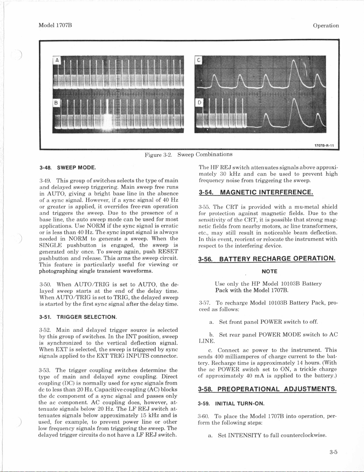
Figure 3-2. Sweep Combinations
3-48.
SWEEP MODE.
The HF REJ switch attenuates signals above approximately 30 kHz and can be used to prevent high
3-49. This group of switches selects the type of main
frequency noise from triggering the sweep.
and delayed sweep triggering. Main sweep free runs
in AUTO, giving a bright base line in the absence
of
a
sync signal. However, if a sync signal of 40 Hz
or greater
and triggers the sweep. Due to the presence of
is
applied, it overrides free-run operation
a
base line, the auto sweep mode can be used for most
applications. Use NORM if the sync signal is erratic
or is less than 40 Hz. The sync input signal is always
i
needed in NORM to generate a sweep. When the
SINGLE pushbutton is engaged, the sweep
is
3-54. MAGNETIC INTERFERENCE.
3-55. The CRT is provided with a mu-metal shield
for protection against magnetic fields. Due to the
sensitivity
netic fields from nearby motors, ac line transformers,
etc., may still result in noticeable beam deflection.
In this event, reorient or relocate the instrument with
respect to the interfering device.
of
the CRT,
it
is possible that strong mag-
generated only once. To sweep again, push RESET
pushbutton and release. This arms the sweep circuit.
3-56. BATTERY RECHARGE OPERATION.
This feature is particularly useful for viewing or
photographing single transient waveforms.
3-50. When AUTOA'RIG is set to AUTO, the delayed sweep
When AUTO/TRIG
starts
at
the end of the delay time.
is
set to TRIG, the delayed sweep
is started by the first sync signal after the delay time.
Use only the HP Model 10103B Battery
Pack with the Model 1707B.
To recharge Model 10103B Battery Pack, pro-
3-57.
NOTE
ceed as follows:
3-51.
TRIGGER SELECTION.
a. Set front panel POWER switch to off.
3-52. Main and delayed trigger source
by this group of switches. In the INT position, sweep
is synchronized to the vertical deflection signal.
When EXT is selected, the sweep
is
signals applied to the EXT TRIG INPUTS connector.
is
selected
triggered by sync
b. Set rear panel POWER MODE switch to AC
LINE.
Connect ac power to the instrument. This
c.
sends 400 milliamperes of charge current to the battery. Recharge time is approximately 14 hours. (With
3-53. The trigger coupling switches determine the
type of main and delayed sync coupling. Direct
coupling (DC)
dc to less than
is
normally used for sync signals from
20
Hz. Capacitive coupling (AC) blocks
the ac POWER switch set to ON, a trickle charge
of
approximately
40
mA is applied to the battery.)
3-58. PREOPERATIONAL ADJUSTMENTS.
the dc component of a sync signal and passes only
the ac component. AC coupling does, however,
tenuate signals below
tenuates signals below approximately
)
used, for example, to prevent power line or other
20
Hz. The LF REJ switch
15
kHz and is
atat-
3-59.
INITIAL TURN-ON.
3-60.
To
place the Model 1707B into operation, per-
form the following steps:
low frequency signals from triggering the sweep. The
delayed trigger circuits do not have
a
LF
REJ switch.
Set INTENSITY to full counterclockwise.
a.
3-5
Page 25
Operation
b. Set vertical POSITION A and B to midrange.
Set DISPLAY to desired mode of operation.
c.
d. Set VOLTS/DIV to 5V
Set channel A and B verniers to CAL detent.
e.
Place B POLARITY to NORM.
f.
Set vertical coupling channel A and B to
g.
GND.
Set HORIZONTAL POSITION to midrange.
h.
Set main TIME/DIV to 1 mSEC.
i.
Set delayed TIME/DIV to OFF.
j.
k.
Set main and delayed VERNIER to CAL
detent.
Set main AUTO/NORM to AUTO.
1.
Set main INT/EXT to INT
m.
Set sweep display to MAIN sweep.
n.
Verify
MODE
0.
Apply operating power and allow 15 minutes
warm i'up time.
Set INTENSITY
p.
Connect signal(s) and proceed with meas-
q.
urements.
3-61.
FOCUS
To adjust FOCUS and ASTIGMATISM pro-
3-62.
ceed as follows:
a. Set all pushbuttons out.
b. Set Model 1707B channel A controls as
follows:
proper position of POWER
switch located on rear panel.
so
that trace
AND ASTIGMATISM ADJUST.
is
just visible.
Model 1707B
0
3-63.
3-64. Figure 3-5 through 3-7 are operating plates
containing step-by-step operating procedures indexed
to photographs.
PE RAT1
N
G
PRO C
E
D
U
RES.
3-65. OPERATORS PERFORMANCE
CHECK.
3-66. The operation of the Model 1707B may be
checked without use of additional test equipment by
using the CAL 1 VOLT output
These operating tests will functionally check each of
the display modes and the front-panel controls. To
check specifications listed in table
V for performance checks. The operation check must
be performed in the sequence given. Do not attempt
to
start a procedure in mid-sequence,
steps depend on control settings and results of previous steps. If any of the results are unobtainable,
refer to Section V, Performance Checks and Adjustment Procedure, or Section VIII, Schematics and
Troubleshooting.
Set Model 1707B controls as follows:
a.
channel A VOLTS/I)IV
channel A coupling
channel A vernier..
DISPLAY.
trig..
B POLARITY..
main VERNIER
delayed VERNIER.
sweep display.
main TIMWDIV.
delayed TIME/DI
DELAY TIME
AUTO/NORM
main INTiEXT
delayed INT/EXT..
delayed slope
........
.....................
...................
...
............
...................
......................
......................
.........................
main TRIGGER LEVEL
TRIGGER HOLDOFF
SWP
MAG
.......................
as
a
signal source.
1-1,
refer to Section
as
succeeding
...............
.......
.......
................
A ONLY TRIG
NORM
..............
.........
........
..............
.5 mSEC
AUTO
..................
......
for stable triggering
............
as
required
NORM
.02
A
CAL
INT
INT
+
t
VOLTS/DIV
DISPLAY..
POSITION
c. Set main TIME/DIV to
d. Turn main vernier full ccw.
e. Set INTENSITY to observe dot.
f. Adjust FOCUS and ASTIGMATISM controls
for best defined dot,
3-6
..........................
............................
..........
as
dot moves slowly across CRT.
center trace on CRT
.2
SEC.
.01
A
b. Set INTENSITY, FOCUS and POSITION con-
trols for desired display in center of screen.
C.
Connect CAL 1 VOLT output to channel A
INPUT using the
d. Adjust main TRIGGER LEVEL for stable
display. Observe approximately 5 positive-going
pulses with an amplitude of 5 div.
e. Set delayed TIME/DIV to
intensified portion of sweep.
XI0
probe.
.2
mSEC. Observe
Page 26
Model 1707B Operation
‘j
Intensified portion should cover 4
to 5 divisions.
Adjust DELAY TIME until intensified portion
f.
is centered on CRT.
g. Set sweep display switch to DELAYED
SWEEP. Observe that intensified portion
to full
10
divisions.
Set sweep display switch to MAIN SWEEP.
h.
Vary DELAY TIME control. Observe that in-
i.
tensified portion moves smoothly along display.
j.
Set delayed AUTO/TRIG control to TRIG.
k.
Adjust delayed TRIGGER LEVEL for stable
intensified portion of the trace.
1.
Vary DELAY TIME control. Observe that
leading edge of intensified portion jumps from one
positive slope leading edge to next.
Set delayed TIME/DIV to OFF.
m.
\
l
n. Rotate main VERNIER counterclockwise to
stop. Observe
and eleventh graticule lines.
Disconnect calibrator signal from vertical am-
0.
plifier.
NOTE
is
15
or more pulses between first
expanded
3-69. AUTO VERSUS NORM.
3-70.
In AUTO operation, there will always be a base
line. A trigger signal of
AUTO operation and produces
40
Hz
or
higher overrides
a
stable presentation. Adjustment of main TRIGGER LEVEL may
be necessary for a stable display. If the trigger
less than 40
tion should be used. A trigger signal
Hz,
or if
it
is
unstable, NORM opera-
is
always
needed in NORM operation to generate a sweep.
3-71. AUTO VERSUS
TRIG.
3-72. Auto delayed sweep operation is achieved
when
AUTO/TRIG pushbutton
the delayed sweep to start
time
as
set by the DELAY TIME control.
3-73. AC VERSUS DC.
3-74.
Ac coupling removes the dc level of trigger
is
out. This causes
at
the end of delayed
signals operations. Use of the LF RE J control prevents
low frequency noise from triggering the sweep.
3-75. MIXED SWEEP.
3-76. In this mode, the first part of the present-
ation is displayed on a time base set by the main
TIME/DIV switch. The last part of the presentation
is displayed on a time base set by the delayed TIME/
DIV switch. The delay between the
main sweep and the start of the delayed sweep
start
of the
is
determined in part by the DELAY TIME control.
3-77. DELAYED SWEEP.
is
Set main TIME/DIV to
p.
Set main TRIGGER LEVEL to full clockwise
q.
position.
Set main AUTO/NORM to NORM.
r.
s.
Select SINGLE operation.
t. Press RESET pushbutton. Reset indicator
should go on. Observe no sweep.
Rotate main TRIGGER LEVEL to full counter-
u.
clockwise position. Observe one sweep and reset
indicator goes off after sweep.
v. Set AUTO/NORM to AUTO.
Press RESET pushbutton. Observe one sweep.
w.
3-67.
)
3-68. The following paragraphs provide additional
OPERATING INFORMATION.
information concerning the use of some specific
functions.
.1
SEC.
3-78. Signals can be displayed
at
100
ns/div with
3% accuracy. Displays can also be expanded up to
10
ns/div
(XI0
magnification) with
5%
accuracy.
This expansion permits viewing critical rise time or
signal shapes with increased resolution. The portion
to be expanded
control in main sweep operation.
is
selectable by the DELAY TIME
It
is
then expanded
to the sweep speed selected by the delayed TIME/
DIV switch after delayed sweep operation
is
selected.
Because the sweeps are independent, the main
VERNIER may be out of CAL position while the
delayed sweep is still calibrated.
3-79. Sweep jitter can be reduced by use of the
delayed operation. By using TRIG mode instead of
AUTO in delayed sweep operation, the delayed sweep
starts on a new trigger. This reduces the jitter
that has accumulated since start of the main sweep.
3-80. LINE SYNC.
3-81. Line sync
is
selected by depressing both
main HF REJ and LF REJ pushbutton. This method
of time base synchronization
is
useful when observing
waveforms that are timerelated to the line frequency.
3-7
Page 27
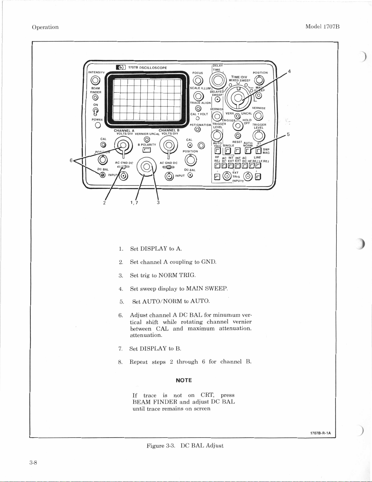
Operation
Model 1707B
2
i,i
1.
Set DISPLAY to A.
Set channel A coupling to GND.
2.
Set trig to NORM TRIG.
3.
4.
Set sweep display to MAIN SWEEP.
5.
Set AUTO/NORM
Adjust channel A DC BAL for minumum ver-
6.
3
to
AUTO.
tical shift while rotating channel vernier
between CAL, and maximum attenuation.
attenuation.
7.
Set DISPLAY to
Repeat steps 2 through 6 for channel
8.
B.
B.
3-8
NOTE
If trace
is
not on CRT, press
BEAM FINDER and adjust DC BAL
until trace remains on screen
Figure
3-3.
DC BAL Adjust
17070-R-1A
Page 28
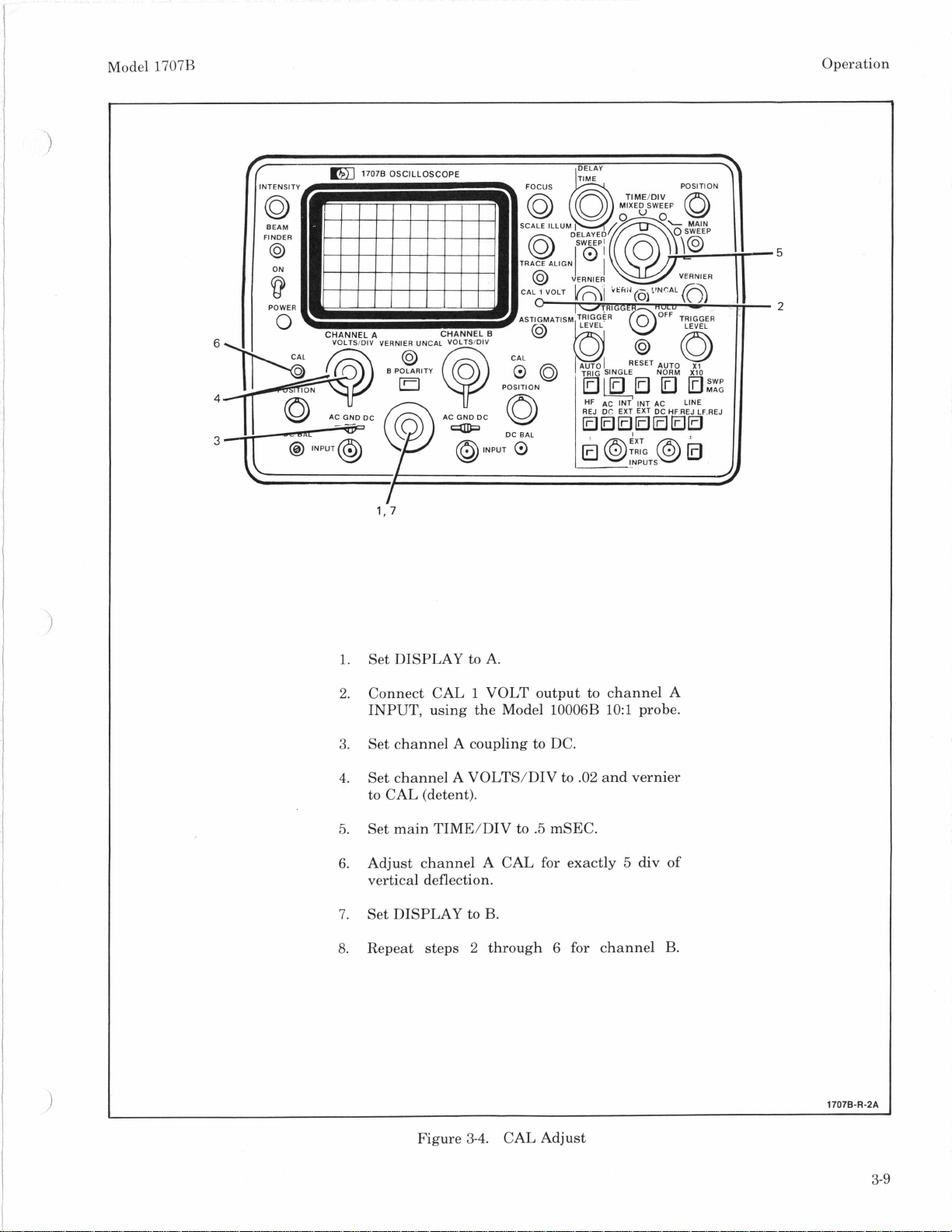
Model 1707B Operation
17078
OSCILLOSCOPE
1
,'7
Set DISPLAY to A.
1.
2.
Connect CAL 1 VOLT output to channel A
INPUT, using the Model 10006B 1O:l probe.
Set channel A coupling to DC.
3.
4.
Set channel A VOLTS/DIV to
!
to CAL (detent).
Set main TIME/DIV to
5.
6.
Adjust channel A CAL for exactly 5 div of
.5
mSEC.
.02
and vernier
vertical deflection.
7.
Set DISPLAY to B.
8.
Repeat steps 2 through 6 for channel
B.
Figure
3-4.
CAL Adjust
3-9
Page 29
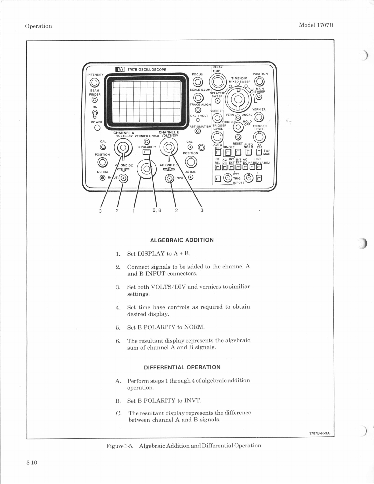
Operation Model 1707B
32
1
1.
Set DISPLAY to A
2.
Connect signals
and B INPUT connectors.
Set both VOLTS/DIV and verniers to similiar
3.
settings.
4.
Set time base controls
desired display.
Set B POLARITY to NORM.
5.
The resultant display represents the algebraic
6.
sum of channel A and B signals.
DIFFERENTIAL OPERATION
Perform steps 1 through 4 of algebraic addition
A.
operation.
5;B
ALGEBRAIC ADDITION
2
+
to
be added to the channel A
3
B.
as
required to obtain
3-10
B.
C.
Figure
Set B POLARITY to INVT.
The resultant display represents the difference
between channel A and B signals.
Algebraic Addition and Differential Operation
3-5.
17078-R-3A
Page 30
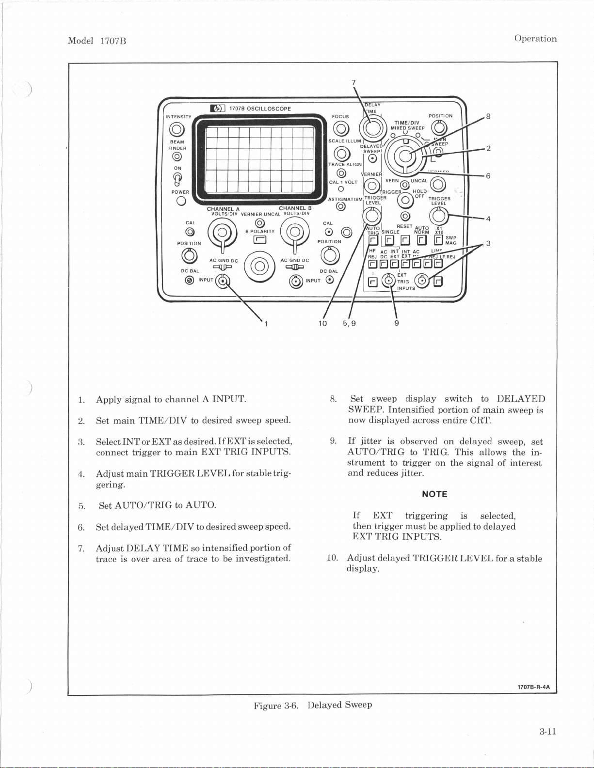
Model
1707B
\-rrr--
1
10
5,9
Operation
7
9
Apply signal to channel A INPUT.
1.
2.
Set main TIME/DIV
Select INT
3.
connect trigger to main EXT TRIG INPUTS.
Adjust main TRIGGER LEVEL for stable trig-
4.
gering.
5.
Set AUTO/TRIG to AUTO.
Set delayed TIME/DIV to desired sweep speed.
6.
7.
Adjust DELAY TIME
trace is over area
or
EXT as desired. If EXT is selected,
to
desired sweep speed.
so
intensified portion
of
trace to be investigated.
of
8.
Set sweep display switch to DELAYED
SWEEP. Intensified portion of main sweep is
now displayed across entire CRT.
9.
If jitter is observed
AUTO/TRIG
strument
and reduces jitter.
If EXT triggering is selected,
then trigger must be applied to delayed
EXT TRIG INPUTS.
10. Adjust delayed TRIGGER LEVEL for a stable
display.
to
to
trigger on the signal of interest
on
delayed sweep, set
TRIG. This allows the in-
NOTE
Figure
3-6.
Delayed Sweep
17076-R-4A
3-11
Page 31

Operation
Model 1707B
1
1.
Connect the signal to channel A INPUT.
Set trig to A ONLY TRIG or NORM TRIG,
2.
2
3
as
desired.
Set main and delayed INT/EXT
3.
as
desired. If
EXTis selected, connect trigger signals to main
and delayed EXT TRIG INPUTS.
Set main and delayed TIME/DIV
4.
to
desired
sweep speeds.
Adjust main and delayed TRIGGER LEVEL for
5.
stable triggering.
6.
'Set sweep display to MIXED SWEEP.
7. Adjust DELAY TIME until desired waveform
combination is displayed.
3-12
17076-R-SA
Figure 3-7. Mixed Sweep
Page 32

Model 1707B
Theory
4-1.
4-2. This section contains functional descriptions
keyed to
and simplified block diagrams of circuit groups. A
detailed explanation of circuit functions, keyed to the
schematics, is provided after the block diagram dis-
cussion. The schematics are located in Section VIII.
4-3.
4-4. An overall explanation of circuit operation
based on block diagrams (schematics 1 and 2)
sented to generate a basic understanding of the
instrument. For simplicity, the block diagrams are
drawn for function and do not show all circuit details.
4-5. This instrument consists of
rectifier, gate assembly, and three modules. The
modules are as follows:
containing attenuators, vertical preamplifier, delay
1
line, and vertical output amplifier;
amplifier module containing trigger assembly, horizontal mother board, main and delayed integrators,
main and delayed sweep time assemblies, holdoff
and comparator assembly, horizontal mode assembly,
horizontal preamplifier, and horizontal output ampli-
fier; and
voltage mother board, low voltage converter, low
voltage rectifier and filter, high voltage oscillator,
and high voltage multiplier.
4-6. INPUT ATTENUATOR. (See schematic 1.)
4-7. The attenuators are compensated voltagedivider types. They provide division ratios of 1, 2,
10, and 100, giving nine separate sensitivities. Each
decade, input sensitivity range has an input capacitance adjustment and an attenuator compensation
adjustment. Coupling (AC, GND, and DC) is also
controlled in the attenuator stages.
4-8. VERTICAL PREAMPLIFIER.
4-9. The vertical preamplifier provides amplification to the input signals for drive to the vertical
output amplifier. Channel A sync and composite sync
signals originate in the vertical preamplifier. The
sync signals are applied to the trigger assembly for in-
)
ternal triggering. Channel switching, chop operation,
and display mode are also accomplished in the vertical preamplifier (schematic
INTRODUCTION.
an
overall block diagram of the instrument,
BLOCK DIAGRAM DISCUSSION.
a
(1)
vertical amplifier module
(2) a horizontal
(3)
power supply module containing low
7).
SECTION
IV
PRINCIPLES OF OPERATION
4-10. DELAY LINE.
4-11.
The delay line provides approximately 160-11s
delay to the vertical signal, allowing the horizontal
circuits sufficient time to react to the trigger signal
so
that the event caused by the trigger can be
observed on the fastest sweep.
4-12. VERTICAL OUTPUT AMPLIFIER.
4-13.
The vertical output amplifier provides drive
to
the CRT vertical deflection plates.
4-14. TRIGGER CIRCUITS.
is
pre-
CRT, line
5,
4-15. The trigger assembly provides the main and
delayed trigger signals to the integrators. Trigger
modes are selectable in this assembly. The main
trigger circuit provides two outputs to the main integrator (schematic
trigger that is generated by the trigger gate driver.
The output of the trigger gate driver is controlled
by the inputs to the gated Schmitt trigger. One input
to the gated Schmitt trigger is the trigger signal and
the other input
grator. When the reset signal is high, the gated
Schmitt trigger is inoperative and no trigger signal
is generated. When the reset signal is low, the gated
Schmitt trigger
will be generated if there is an internal or external
trigger input. The other output is the brightline auto level which is provided only in the auto mode.
The delayed trigger circuit functions identically to the
main trigger circuit and provides a trigger signal
to the delayed integrator (schematic
4-16. MAIN INTEGRATOR.
4-17. The main integrator initiates a horizontal
sweep from the trigger input. When the trigger signal
is applied
activates and produces the horizontal sweep ramp.
The Miller integrator is connected to the main sweep
timing components (schematic
DIV
integrator. The output of the Miller integrator is amplified and applied to the horizontal amplifier circuits.
4-18. The horizontal sweep is also compared to
volt reference by the ramp comparator which drives
the main integrator set-reset multivibrator. The setreset multivibrator, in conjunction with the holdoff
and comparator circuit, controls the amplitude and
timing sequence of the sweep ramp. When the
to
the gate amplifier, the Miller integrator
switch controls the ramp output from the Miller
1).
One output is the main
is
the reset signal
is
operational and a trigger signal
from
the main inte-
12).
11).
The main TIME/
a
12-
4-1
Page 33

Theory
Model
1707K
sweep ramp reaches
turns on and resets the gated Schmitt trigger to
logic high
(1).
+12
volts, the ramp comparator
a
The signal from the holdoff amplifier
determines the holdoff time of the circuits and sets
the gated Schmitt trigger to a logic low
(0)
for
a
new sweep.
4-19.
When the bright-line auto circuit is used, the
set-reset multivibrator provides a ground for the
bright-line auto level and terminates the sweep. This
allows the sweep signal to return to its starting point.
4-20.
At the same time that the main ramp
is
generated, the alt amplifier provides an output to the
vertical preamplifier flip-flop for alt operation.
4-21. HOLDOFF AND COMPARATOR.
4-22.
The holdoff and comparator establishes the
time interval between trigger points. The time interval is adjusted by the TRIGGER HOLDOFF control.
A
signal from the main integrator set-reset multivibrator activates the holdoff circuit. When the holdoff
is activated, a ramp, determined by the holdoff amplifier
RC
circuits and the TRIGGER HOLDOFF control,
is generated. When this ramp reaches a predetermined
level, it activates the main integrator set-reset multivibrator. The set-reset multivibrator then sets the
trigger set-trigger gates low for a new sweep.
4-23.
The main horizontal sweep ramp from the
Miller integrator also drives the comparator in the
holdoff and comparator assembly. The main sweep is
compared to a voltage set by the DELAY TIME dial.
When the main sweep is equal to this voltage, the
Schmitt trigger sends a pulse to the delayed integrator set-reset multivibrator. This sets the delayed
gated Schmitt trigger low and arms the delayed integrator for a new sweep.
4-24. DELAYED INTEGRATOR.
4-25.
The delayed integrator operates the same as the
main integrator, except for the following differences.
This circuit has no bright-line auto input. In the auto
mode, a voltage is applied to the input amplifier which
activates the Miller integrator for a delayed sweep
signal. The Miller integrator is connected to its own
RC components for generating the delayed sweep.
Sweep limits are set by a comparator and set-reset
multivibrator as in the main integrator.
4-26.
The set-reset multivibrator has an input from
the main integrator set-reset multivibrator. If the main
sweep terminates, a voltage from the main integrator
is sent to set-reset multivibrator. The multivibrator terminates the delayed sweep and
arms the
delayed gated Schmitt trigger for a new sweep.
INTERNALSYNC
SET-RESET
MULTIVIBRATOR
GATED SCHMITT
TRIGGER INPUT
GATEDSCHMITT
TRIGGER OUTPUT
OUTPUT
INTEGRATOR E
MAIN
OUTPUT
HOLDOFF
AMPLIFIER F
IN PUT
TO TI T2
I
A
I
I
B
I
I
I
I
I
D
I
II
11
11
I
I
II
II
ii
T3 T4 T5
1
I
I
II
II
I
1
1703A-E-1B
4-2
Figure
4-1.
Timing Sequence
Page 34

Model
1707B
Theory
4-27. TIMING SEQUENCE.
4-28.
Figure 4-1
is
an illustration representing the
time relationship between the trigger and sweep
timing circuits.
Waveform A represents the input
signal to the vertical circuits and the internal sync
signal. Waveform B represents the main integrator set-
reset multivibrator output. Waveform C represents the
input
to
the gated Schmitt trigger and waveform
D
represents the output. Waveform E represents the input to the holdoff and amplifier.
4-29,
At
To,
the multivibrator output
is
high,
holding the gated Schmitt trigger high, preventing
;I
sweep signal. At Ti, the holdoff time
is
completed and the multivibrator output goes low, activating
the gated Schmitt trigger. At T2, the trigger signal
goes
positive and the gated Schmitt trigger output
goes
low, activating the main integrator which pro-
duces a horizontal sweep signal.
+:(O.
At
'I';j,
the sweep
is
terminated and the setreset multivibrator output goes high. When the setreset multivihrator goes high, the holdoff time signal
starts and the gated Schmitt trigger is locked high,
preventing a sweep. At the completion of holdoff
time, the sequence
is
repeated.
4-37. The line rectifier rectifies and filters the power
transformer ac output of approximately 36 volts. This
voltage
is
applied to the voltage regulator and
ripple filter which filters out the 120-hertz ripple.
4-38. The voltage regulator output
is
applied to the
low voltage converter. This stage converts the input
dc power to usable output dc of different voltage
levels. The low voltage converter oscillates between
10 kHz and 45 kHz, depending upon the input voltage
and the output power.
4-39. The voltage coupled from the converter to the
low voltage rectifier
is
filtered and applied to the
low voltage mother board which provides low voltage
distribution to the power supply module. A portion of
the
t15
and -15 volts
is
fed back to the low voltage
regulator which determines the frequency and duty
cycle of the converter for output voltage regulation.
4-40. The filtered voltages from the low voltage
mother board are coupled to the gate board. The gate
board provides filtering, fuse protection and distribution of the low voltage supplies to the rest of the
Model 1707B circuits.
4-41. HIGH VOLTAGE POWER SUPPLY.
a
4-31. HORIZONTAL MODE ASSEMBLY.
4-42. The high voltage power supply consists of the
high voltage oscillator, power transformer, rectifying
4-:12.
i
This assembly controls main sweep, mixed
sweep, delayed sweep, external horizontal input and
the trace intensity in these modes. A switch selects
the type of sweep signal to be displayed.
networks, and high voltage multiplier. When the
instrument
is
turned on, the high voltage oscillator activates, coupling voltages from pins 1 and 2 into the
secondary pins 6 and
7,
5,
8, and
9.
Pins
11
and 10
are connected to filaments of the CRT. The secondary
4-:{3.
The blanking circuit blanks the trace in the
main sweep, delayed sweep and mixed sweep modes.
The blanking signal is applied to the gate assembly
(schematic
2)
which controls the high voltage oscil-
lator assembly.
4-:M.
In the
EXT
HOKIZ INPUT mode, the blanking
signal
is
grounded and the output from the external
horizontal amplifier is connected to the horizontal
voltage
at
pin
7
is
connected through arectifying diode
to the control grid of the CRT. Pin 8 of the secondary
is
connected through a rectifying diode to the cathode.
A correction voltage
is
coupled from this diode back
through a resistive divider network, controlling the
current source. The current source controls the oscillator amplitude and thus the high voltage oscillator
output. The CRT voltages are negative, except for the
post-accelerator voltage.
preamplifier. The blanking circuit also intensifies the
delayed portion of the sweep in the main sweep
and mixed sweep mode. When the delayed TIME/
1)IV switch
is
set to some position other than
OFF,
the main sweep intensity is reduced and the delayed
sweep intensity is held at a normal level, providing
trace intensification.
4-35. LOW VOLTAGE POWER SUPPLY. (See schematic
2.)
4-36.
The low voltage power supply operates from
three different power sources. The sources are ac
line, internal battery or external dc line. The ac line
is applied to the input power module which
,i
able for 115- or 230-volt operation and has an ac
line protection fuse. The ac input
is
is
select-
applied to
a
step-down power transformer.
4-43. The CRT cathode voltage
is
fed back to the current source. If the cathode voltage becomes more
negative, less current
is
supplied to the high voltage (hv) oscillator. With less current supplied, the
amplitude of the hv oscillator output
is
reduced and
the cathode voltage will return to its normal operating
value. If the cathode voltage becomes less negative,
more current
is
supplied to the hv oscillator. The output amplitude now increases and the cathode voltage
again returns to
6.73 kV peak-to-peak voltage
the high voltage transformer. This voltage
to the high voltage multiplier circuit where
multiplied by,3. The
its
normal operating value. A
is
present
at
is
20.2
kVoutput
is
applied
pin 9 of
applied
it
is
to
the
post-accelerator on the CRT.
4-3
Page 35

Page 36

Model 1707B
Theory
1
turn on. This clamps the emitters
A5A4Q23 to approximately t6 volts, turning them off.
When A5A4Q20 is turned off, its emitter approaches
0
volt and the diodes turn off. This permits the
emitters of A5A4Q221A5A4Q23 to fall to approxi-
mately t4.2 volts, turning the transistors on.
4-65. The channel B switch consists of normal output
amplifier A5A4Q25/A5A4Q26, inverted output amplifier A5A4Q24/ASA4Q27, and transistor switch
A5A4Q21. Transistor switch A5A4Q21 functions
exactly as explained in paragraph 4-64 for A5A4Q20.
Depending on the position of B POLARITY switch
A5S1, the normal output amplifier or the inverted
output amplifier will turn on, but not both. When
A5A4Q20 is turned off and A5A4Q21 is turned-on,
only the channel A signal appears at the output of
the channel switches. When A5A4Q20
and A5A4Q21 is turned off, only the channel B signal
appears at the output. When both A5A4Q20 and
A5A4Q21 are turned off, the algebraic sum
channel A and channel B signals appears
output. If the normal output amplifier
of the channel switches
If the inverted output amplifier
the channel switches is the difference between the
two signals.
4-66. Feedback amplifier A5A4Q28IA5A4Q29 am-
plifies the composite signal and drives the delay
line driver. The feedback circuits improve frequency
response by compensating for collector-to-base
capacitance.
4-67. The channel A sync amplifier consists of
A5A4Q18, A5A4Q19, and A5A4Q17. Its inputs are
from the channel A amplifier on schematic 4 and
its output
matic 7.
is
to
the sync selection circuits on sche-
is
the sum of the signals.
of
A5A4Q22/
is
turned on
is
on, the output
is
on, the output
of
at
the
the
of
and three inputs. When
A5A4U2 acts as an asynchronous flip-flop and the
a
output
C
is low, A5A4U2 again acts
flip-flop and the2 output
C
are low, both Q and Q are high. When both S and
C
are high, A5A4U2 acts
tive going transition on T will cause the flip-flop
change states.
4-71. The astable multivibrator
A5A4UlA and A5A4UlB. In all positions of the display switch, except chop, the astable multivibrator
is disabled because pin 2 of A5A4UlA
(held low) by the front section of A5S2A. In the
chop position, the ground is removed and pin 2 goes
high. During sweep time, the alt trigger
Because both inputs are now high, the output of
pin 3 is low. Pin 6 of A5A4UlB is high and the
astable multivibrator is running.
4-72.
The clocked flip-flop is driven by A5A4UlC and
A5A4UlD. In the A, B and A + B positions of the
DISPLAY switch, the T input to the clocked flip-flop
is held high because pin 9 of A5A4UlD is grounded
(held low) by the rear section of A5S2A.
A,
the S input of A5A4U2
section of A5S2C and A5A4Q36 is turned on. In
position
section of A5S2C and A5A4Q37 is turned on. In
position A + B, both S and C are grounded and both
A5A4Q36 and A5A4Q37 are turned on.
4-73.
In
PLAY switch, the S and C inputs of A5A4U2 are
ungrounded and go high. Pin 9 of A5A4UlD
ungrounded and goes high. In these positions, changes
at pin 10 of A5A4UlD control the state of the flip-flop.
is
high. When
B,
the
C
input is grounded by the rear
the CHOP and ALT positions of the DIS-
C
is
high and S is low,
S
is high and
as
an asynchronous
is
high. When both S and
as
a
J-K
flip-flop and a nega-
is
driven by
is
grounded
In
is
grounded by the front
is
high.
position
is
also
to
4-68.
Schematic
cuits (A5A4Q32/A5A4Q33) amplify the composite signal and drive the delay line. Amplifier A5A4Q30/
A5A4Q31 selects and amplifies the composite sync
signal. The composite sync signal drives the sync
selection circuits on schematic 7.
4-69.
Schematic
7 control the channel switches (schematic
chop blanking, and select the trigger signal.
4-70. The steering logic circuits control the channel
gates and generate chop blanking. Astable multivibrator A5A4Q34IA5A4Q35 is activated when the
base of A5A4Q34 is high. It free-runs at approximately
800
kHz. When the base is low, it is prohibited from
running. A5A4Q36 controls the channel A gate
(schematic 5) and A5A4Q37 controls the channel
gate. A5A4U1 is a four-section integrated circuit (IC)
consisting of four NAND gates. Three of the four
I
sections operate conventionally but, because its two
inputs are tied together, A5A4UlB functions simply
as
an inverter. Flip-flop A5A4U2 has two outputs
6.
The vertical preamplifier cir-
7.
The circuits shown on schematic
5),
generate
B
4-74. In the
inultivibrator is permitted to free-run, its output
being routed
when the alt trigger is present, the output of the
astable multivibrator will cause the clocked flip-flop
to change states at each negative transition. The net
result being that the channel switches (schematic
change between channel A and channel B at a 400kHz rate.
4-75. In the ALT position of A5S2, the astable
multivibrator is again disabled and pin 12 of
A5A4U1 C is held high. Each negative-going transition of the alt trigger causes the clocked flip-flop
to change states. The net result being that the channel switches (schematic
between channel A and channel B.
4-76. The chop blanking output of the astable
multivibrator is routed via the circuits on schematic
17 to the CRT blanking circuits
during the channel switching transitions.
CHOP
to
position of A5S2, the astable
pin 12 of A5A4UlC. During the time
5)
alternate,
at
the sweep rate,
to
blank the CRT
5)
4
-5
Page 37

Theory
Modcl 1707K
4-77. The NORMTRIG/A
ONLY
TRIGswitch selects
either channel A trigger from schematic 5 or the composite trigger from schematic
6.
A5A4Q38 and
A5A4Q39 drive the main trigger circuit on schematic
8.
4-78. In the A + B position
the B section connects
A
+
I3
BAL potentiometer (schematic
of
th-e DISPLAY switch,
+15
volts (schematic 4)
5).
This permits
to
the
correction of any dc unbalance caused by turning
both the channel A and channel B switches on
together.
4-79.
DELAY LINE.
4-80. The delay line (schematic 6) provides 160
nanoseconds delay to the vertical signal. This offsets
the delay in the trigger and gating circuitry and
assures that part of the vertical signal is not lost
before these circuits react and
4-81. VERTICAL OUTPUT AMPLIFIER.
start
the sweep.
4-82. The vertical output amplifier (schematic 6)
consists of differential amplifiers A5A5Ql/A5A5Q2
with current source A5A5Q3, feedback amplifier
A5A5Q4/A5A5Q5, and cascade differential amplifier
A5A5Q6 through A5A5Q9. The amplifier receives the
composite signal from the delay line and drives the
vertical deflection plates of the CRT.
4-83.
Optimum high frequency response
is
obtained
from the amplifier by adjusting hf comp adj
A5A5C7, hf peak adj A5A5R30, and hf adj A5A5C12.
4-84. The feedback circuits of A5A5Q4 and A5A5Q5
improve frequency response by compensating for
collector-to-base capacitance.
4-85.
The BEAM FINDER switch limits the current
available
to
the differential amplifier. This reduces
the overall gain and assures that the beam will not be
deflected off screen when the BEAM FINDER
is
pressed.
4-86. TRIGGER CIRCUITS.
4-87.
The trigger assembly (schematics 8 and
9)
consists of the main and delayed trigger circuits.
Inputs are selected from the internal sync circuits
in the vertical amplifier, from the main EXT TRIG
INPUT, or from the delayed EXT TRIG INPUT. Two
outputs, the main trigger signal and the bright line
auto signal, are provided to the main integrator. The
delayed trigger signal
is
provided to the delayed
integrator.
4-89. The main INT/EXT switch selects a signal
from the circuits on schematic 7 or from the main
EXT TRIG INPUT.
4-90. The main AC/DC switch connects A6A2C1
in series for capacitive coupling or bypasses
it
for
direct coupling.
4-91. The main
LF
REJ switch (not used in delayed)
bypasses the frequency limiting circuit A6A2C12/
A6A2Rl or activates
it
to reject trigger frequency
components below 15 kHz.
4-92. The main HF
REJ
switch either bypasses the
frequency limiting network (A6A2R72/stray capacitance) or connects it
to
reject trigger frequency com-
ponents above 30 kHz.
4-93. The main slope switch reverses the inputs
to
A6A2Q1 and A6A2Q2. This permits triggering on
either slope of the trigger waveform.
4-94. The main TRIGGER LEVEL control permits
selection of the point on the trigger slope that initiates
the sweep.
It
accomplishes this by shifting the static
dc level of the main trigger amplifiers.
4-95. The FET source followers, A6A2QWA6A2Q2,
provide the high impedance required to prevent
loading of the trigger sources.
4-96. The emitter followers, AGA2Q3/A6A2Q4, provide the required low impedance drive to the differential amplifiers.
4-97. The differential amplifiers, A6A2Q5 through
A6A2Q8, drive the trigger gate drivers (schematic
9).
4-98.
The trigger gate drivers, gated Schmitt triggers,
and the trigger outputs for main and delayed are
nearly identical
so
only the main circuits will be
discussed. The bright line auto circuit will be explained separately.
4-99. Schematic 9.
The trigger gate drivers,
A6A2Q17 and A6A2Q18 are a differentially driven
differential amplifier whose static dc level
is
closely controlled.
4-100. The gated Schmitt trigger, A6A2UlA and
A6A2UlB, consists of two OR circuits with biasing
and feedback to cause them to function
as
a
Schmitt
trigger. A step-by-step explanation of the gated
Schmitt trigger is given in figure 4-2. The gated
Schmitt trigger has two functions; to generate
a
signal to initiate the sweep upon receipt of a trigger,
and to prohibit further triggering during sweep and
holdoff.
4-88. Schematic
8.
The main trigger circuits and the
delayed trigger circuits are nearly identical, only
the main trigger circuits will be explained.
4-6
4-101. The threshold voltage for the gated Schmitt
trigger is set by the main trigger sensitivity adj
A6
A2
R46.
Page 38

Model 1707B
Theory
TRIG
-
IN
TRIG IN
018
BASE
TRIG
IN
BASE
017
FROM SETRESETMULTIVIBRATOR
TO UlA
U1B PIN 13
+0
I
I
I
1
I
I----'
I
I
I
FROM SET-RESET
MULTIVIBRATOR
1
I
I
I
I
I
I
I
I
TRIGGER
!I
I
I
I
I
I
--
II
!1
1
I
I
-+15V
RULES FOR
If any input
1.
is
2. If all inputs are
SWEEP PERIOD
1.
Main sweep begins (to).
(to
OR
HI, output
LO,
to
tl)
GATES
is
HI.
output is
2. Trigger inputs (waveforms A and B) from
Q17 and QlS are latched below the Schmitt
threshold (waveforms D and
3.
All inputs to UlA and UlB are
4.
Main trigger output
HOLDOFF PERIOD
1.
The sweep ends
(tl
to
(tl)
tp)
is
E).
LO.
HI (waveform
and the sweep com-
parator (schematic 10) resets the set-reset
multivibrator. Holdoff begins.
2. Pins 1 and
3.
Pins 6 and 8 of U1 go HI (rule
13
of U1 follow the reset level HI.
1).
This
causes:
Q19 turns off, main trigger output (wave-
a.
form
G)
goes
LO,
(schematic 10)
Pins 4 and 10 of U1 are unlatched. Their
b.
and the integrator
is
disabled.
levels may now go above and below the
threshold level
changes (waveforms D and
4RMED PERIOD
After holdoff ends, the set-reset multivibrator
1.
sets
LO.
The next
2.
(pin
4)
(tp
LO
(from Q17) on the arming input
causes the output of U1A
to
tg)
as
the trigger input
E).
to
go
(rule 2) and latch.
LO.
G).
LO
PIN4,UlA
U1B OUT
MAIN TRIGGEROUT
U1B now has two
3.
I
from Q18 will cause the output of U1B to go
LO
(rule 2) and latch.
When UlB goes
4.
trigger goes HI (waveform
LO
LO
(waveform
inputs. The next
F),
G)
the main
and the inte-
LO
grator turns on to reinitiate the entire process.
VOTES
1.
I
FI
I
I
G
I
I
I
I
I
I
11
11
Latching occurs whenever the output
OR
gate goes
R1
(or R2)
LO.
The
LO
is
to
the collector of Q17 (or Q18).
coupled through
This assures that the output of the transistor
will never rise to the threshold voltage
varies with the trigger input. Conversely, the
circuit unlatches when the output of the
circuit goes
HI.
This permits the positive
of
as
an
it
OR
excursions of the trigger waveform to rise
above the threshold level.
2.
The threshold level of this circuit is critical
to proper operation. R3 permits adjustment of
the threshold level.
Figure
17078-C-2
4-2.
Step-by-step Operation ofthe Gate Schmitt Trigger
4-7
Page 39

Theory
Model 1707B
4-102. The trigger output, A6AZQ19/A6A2Q20,
functions exactly like the trigger gate driver (paragraph 4-99).
4-103. When pin 8 of A6A2UlB goes low and
A6A2Q19 turns on, pin 9 goes high and A6A2Q20
turns off. A6A2Q21 turns on and saturates. If no
further trigger signals are applied, the collector voltage of A6A2Q21 decays through an RC network
consisting of A6A2R54, A6A2Cl1, and A6A2R55.
When the voltage decays to approximately -16 volts,
A6A2CR12 turns on, A6A2Q23 and A6A2Q24 turn
on and Schmitt trigger A6A2&25/A6A2Q26 activates,
supplying current
to
the main integrator gate (sche-
matic 10) through A6A2R60. In this manner, the
sweep
4-104.
is
initiated
MAIN INTEGRATOR.
in
the absence of trigger pulses.
4-105. The main integrator assembly consists of the
main integrator and associated circuits (schematic
lo),
the set-reset multivibrator (schematic lo), and
the main sweep time assembly (schematic
11).
The
main integrator in conjunction with the main sweep
time assembly generates the main sweep ramp, provides main blanking to the horizontal mode assembly
(schematic
15),
and alternate triggering
to
the verti-
cal preamplifier (schematic 7). The set-reset multi-
vibrator terminates the main sweep, terminates the
delayed sweep if the main sweep terminates, and sets
the gated Schmitt trigger (schematic 9) low
to
arm
for a new trigger.
4-106.
the absence of a main trigger,
tive pulse
or bright line auto, turns
Schematic
on
10.
Gate amplifier A6A3Q1, in
is
turned off. A posi-
either of its two inputs, main trigger
it
on. When A6A3Q1 turns
on, its collector approaches 0 volt and A6A3CR5,
A6A3CR6, and A6A3CR9 turn on. This initiates main
blanking, alternate trigger, and main sweep.
4-107. When A6A3CR5 turns on, it furnishes
a
ground to the horizontal mode blanking circuit
(schematic
the trace to be seen. When A6A3Q1
circuit is on, blanking the
15).
This turns the
CRT.
CRT
on and allows
is
off, the blanking
4-108. When A6A3CR9 turns on, it causes A6A3CR13 and ramp control A6A3Q6 to turn off, activating
the integrator.
4-109. The Miller integrator consists of the components associated with A6A3Q7/A6A3Q8 (schematic
10) and, according to the position of the main TIME/
IIIV
switch, certain of the main sweep time assembly
components (schematic
of the main TIME/DIV switch
integrating capacitor between the collector
11).
Basically, the function
is
to connect a selected
of
A6A3Q8
and the gate of A6A3Q7. The switch also connects
an integrating resistor between the gate of A6A3Q7
and a calibrated charging voltage. During holdoff and
armed time, A6A3Q6
of A6A3Q7
to
is
turned on, clamping the gate
a
fixed voltage. When A6A3Q6 turns
off, a charging current through the integrating resistor
causes the integrating capacitor to start charging
(negatively). This change
at the output of A6A3Q8
is
integrated and appears
as
a
linear positive-going
ramp. Output amplifier A6A3Q9 drives the horizontal
circuits (schematic 16 via schematic
15).
The ramp
also drives the comparator.
4-110. During holdoff and armed time, A6A3CR12
turned on, clamping the emitter of A6A3Q5, holding
the transistor on, and setting the baseline of the ramp.
When A6A3CR12 turns off, the emitter of A6A3Q5
is
permitted
to
follow
its
base. As the ramp (from
A6A3Q8) rises on the base of A6A3Q5, the emitter
follows. When the ramp voltage equals the voltage
on the base of A6A3Q2 (approximately t12 volts),
the comparator changes states. This establishes the
magnitude of the ramp. The resultant current through
A6A3R6 causes common-emitter amplifier A6A3Q3 to
turn on.
4-111. The set-reset multivibrator (A6A3U1)
is
an
R-S flip-flop composed of two negated output AND
(NAND) gates. A step-by-step explanation of the
operation of the set-reset multivibrator
figure
4-3.
This circuit has several functions. First,
is
shown in
it permits the formation of a main trigger any time
a
trigger pulse arrives during armed periods.
this by providing a low (from its pin 6 output)
1
of
the set-trigger Schmitt (schematic
9).
Secondly,
It
to
does
pin
it terminates the delayed ramp any time the main
ramp terminates before the completion of the delayed
ramp. It does this
pin 6 of the set-reset multivibrator (schematic
in
the following manner; when
10)
goes high at the end the main sweep, the high
is inverted by A6A3UlC and applied
(as
a
low) to
pin 4 of the delayed set-reset multivibrator (schematic
la),
setting it and terminating the delayed sweep.
Third, it initiates holdoff. It does this by changing
states at the end of sweep time and presenting
high (from pin
6)
to
turn on A6A7Q1 and A6A7Q4
(schematic 14). Fourth, the set-reset multivibrator
prevents the formation of a new main trigger during
holdoff. It does this by presenting the high on pin
6 to pin 1 of the set-trigger schmitt (schematic 9),
disabling it. Finally, it terminates the main sweep
during operation of bright line auto.
follows: when pin 6 goes high
It
does this
at
the end of sweep
as
time, pin 12 goes low. This turns A6A3CFU on, grounding the bright line auto signal and turning A6A3Ql
off.
4-112. The AUTO/NORM switch grounds the bright
line auto input, preventing this circuit from initiating
a sweep.
4-113. The SINGLE switch disconnects the main
enable line. In this condition, the last sweep cycle
proceeds
main enable line
to
condition 3 (figure 4-3) but, because the
is
disconnected, cannot proceed
is
a
4
-8
Page 40

Model
170713
'I'heory
If any input
1.
If
all
2.
RULES
inputs are HI, output is
HI
HI
HI
INITIAL (SET) CONDITION
is
FOR
NAND GATES
LO,
output is HI.
LO.
HI
-LO
(armed and sweep periods)
A6A7Q7
(schematic
14)
is turned off and
pin 1 is HI.
A6AX):I
(schematic 10) is turned off and
pin 5 is HI.
Pin 4 is not connected and is always HI.
Flip-flop is in
HI and pin 6 is
SET
LO.
condition
so
pin 12 is
Pin 3 is HI because it is connected to pin
12.
Pin 2 is
6.
Gate A complies with rule
Crate
LO
because it is connected
I3
complies with rule
to
pin
1.
2.
HI
LO
HI
HI
CONDITION
When sweep retrace starts
pin 5 goes HI.
Gate
H
still complies with rule
flop does not change states.
Flip-flop
At
pin 1 goes
Gate
12
Gate
goes
Flip-flop is again in
is
armed for change on pin
CONDITION
end of holdoff,
A6A7Q7
LO.
A
now complies with rule
goes
HI and pin 3 follows.
I3
now complies with rule
LO
and pin 2 follows.
SET
3
A6A3Q3
HI
-LO
4
condition.
HI
turns off and
1
so
flip-
1.
turns on and
1
so
pin
'2
so
pin
6
HI
HI
LO
LO
HI
AGA3Q:l
goes
LO.
CONDITION
(end
of
(schematic 10) turns on and pin
2
sweep)
Gate H complies with rule 1
HI
and pin 2 follows.
Gate
A
now complies with rule
12
goes
LO.
Flip-flop is in
KMET
condition.
Holdoff time starts
Figure
4-3.
Step-by-step Operation of the Set- reset Multivibrator
HI
so
pin 6 goes
2
so
pin
4
LO
HI
HI
HI
5
A6A7Q7
turns off, permitting pin 1 to go HI.
CONDITION
Gate A still complies with rule
/I
,LO
5
1
so
flip-flop
does not change states.
Flip-flop is still in initial
and is now armed for change on pin
(SET)
condition
5.
Page 41

Theory
Model 1707B
further. The reset switch connects A6AlCl and, during
the initial surge of
is drawn low and the flip-flop goes to condition 4
(figure 4-3).
4-114. Lamp driver A6AlQ1 turns off whenever the
main reset and holdoff line goes low, causing the
RESET lamp (DS2) to light.
4-115.
bly, A6A5, provides selection of an integrating
resistor, an integrating capacitor, and a calibrated
charging voltage for the main integrator (schematic
10).
4-116. Section A of the main TIME/DIV switch,
A6A5S1, selects the integrating resistors for all sweep
speeds, except the five fastest speeds. The resistors
for the five fastest speeds are selected by section
Schematic
its
charging curve, pin 1 of A6A3U1
'.
11.
The main sweep time assem-
B.
4-117. A separate capacitor
two decades of the main TIME/DlV switch. The
and C sections of the switch select all except the
five fastest positions. The integrating capacitor
(A6A3C8) for the five fastest positions
wired into the main integrator circuitry (schematic
10). On all other positions, A6A3C8
with the selected capacitor.
4-1
18.
Operational amplifier A6A5Q1, A6A5Q2, and
A6A5Q3 provides a fixed charging voltage
lector of A6A5Q2. The charging voltage
calibrated for each two decades of the main TIME/
DIV switch. The D section of the switch selects
the calibrating potentiometers.
4-119. HOLDOFF AND COMPARATOR.
is
provided for each
is
permanently
is
in parallel
at
the col-
is
separately
turns on. As the charge on the selected capacitor
starts
to rise, A6A7Q7 turns off. The capacitor quickly
rises to +16 volts.
4-122. Whenever the voltage on the base of A6A7Q2
is less positive than the voltage on the base of
A6A7Q3, A6A7Q2
off. The voltage on the base of A6A7Q3 (and delay
time)
is
selected by DELAY TIME potentiometer
A6R3. When the main ramp rises to equal the selected
voltage on the base of A6A7Q3, the ramp comparator
changes states; A6A7Q2 turns off and A6A7Q3 turns
on. The resultant current through A6A7R7 causes
A6A7Q6 to turn on. At the end of main sweep time,
the circuit returns to the original state. The net
result
that point on the main ramp selected by the DELAY
TIME potentiometer and the end of the main ramp.
At all other times, the collector of A6A7Q6
4-123.
I3
flip-flop formed by two NAND gates and a third
NAND gate connected to function
When A6A7Q6 turns on, its collector goes low and
the Schmitt trigger changes states. The output transition
A6A7R15. The resultant negative-going pulse enables
the set-reset multivibrator (schematic
result is
(relative to the main sweep) selected by the
DELAY TIME potentiometer.
4-124. DELAYED INTEGRATOR.
4-125. The operation of the delayed
matics 12 and 13)
of the main integrator (paragraph 4-104). Only the
exceptions will be discussed.
is
a
low at the collector of A6A7Q6 between
The Schmitt trigger (Ul) consists of an R-S
is
summed and differentiated by A6A7C9 and
that
is
turned on and A6A7Q3 is turned
the delayed sweep
is
nearly identicaI
is
enabled
integrator
to
as
is
high.
an inverter.
12). The net
at a time
(sche-
the operation
1
4-120.
assembly (schematic 14) have two functions: to
determine the time between the end of one sweep
and the arming of the next (holdoff), and
mine the time between the beginning of the main
sweep and the beginning or arming of the delayed
sweep (delay).
4-121. During sweep time, A6A7Q1
and A6A7Q4
by TIME/DIV switch A6A7S1
+16 volts. When the main set and reset voltage (from
schematic
A6A7Q1 turns on and A6A7Q4 turns off. The selected
capacitor starts discharging exponentially through
A6A7R13 and TRIGGER HOLDOFF potentiometer
A6R7. The rate of discharge (and holdoff time)
determined by the setting of A6R7. When the charge
on the selected capacitor has fallen to approximately
0
applies a low to the set-reset multivibrator (schematic
lo),
voltage goes low, A6A7Q1 turns off and A6A7Q4
4-10
The circuits on the holdoff and comparator
to
deter-
is
turned off
is
turned on. The capacitor selected
is
charged
10)
goes high
volt, A6A7Q7 turns on. A6A7CR6 turns on and
enabling
it.
When the main reset and holdoff
at
the end of sweep time,
to
about
is
4-126.
enabled by the delay enable voltage from schematic
14. Because the delay enable voltage does not occur
until that time selected by the DELAY TIME control,
the delayed sweep cannot
TRIG) until arrival of the
selected time.
4-127. When the AUTO/TRlG switch
the delayed sweep starts immediately after delay enable. The AUTO enabling voltage
A6A4CR3 by a low on pin 12 of A6A4UlA. When
the delay enabling voltage causes the set-reset multivibrator to change states, pin
causes A6A4CR3 to turn off and the AUTO enabling
voltage turns A6A4CR1, A6A4CR2, and A6A4Ql on,
initiating the delayed sweep.
4-128.
4-129.
added to the delayed TIME/DIV switch
the delay function. When the delayed TIMEIDIV
Schematic
The output of A6A4UlC
Schematic
12. The set-reset multivibrator
start
first
13.
An OFF position has been
is
(AUTO/TRIG set
trigger pulse after the
is
set to AUTO,
is
grounded through
12
goes high. This
is
not used.
to
to
disable
Page 42

Model 1707B
Theory
switch
Schmitt trigger (schematic 14) to disable
ground
cation (schematic
4-130. HORIZONTAL
4-131. The horizontal mode assembly (schematic
is
set to
is
OFF,
a
ground
is
applied to the
also used to disable the trace intensifi-
15).
MODE.
it.
The
15)
has two functions: sweep selection and blanking. Both
functions are controlled by sweep display switch
A6A8S1.
?-
1,'12.
Siiwp
Selection.
Section
1F
of A6A8S1
selects either the output of the main integrator
(MAIN
SWEEP), the output of the delayed integrator
(1)ELAYEl) SWEEP), the output of both (MIXED
SWEEP), or EXT
HORIZ
INPUT. The selected output
drives the horizontal amplifier (schematic 16).
4-133. Blanking.
The blanking circuit provides
blanking current to gate assembly A4 (schematic
17). Maximum current
in
the blanking output completely blanks the CRT. No current output causes
maximum brightness of the CRT display.
4-134. Figure
part of the circuitry on schematic
circuitry on schematic 17. Current source
4-4
is a simplified schematic showing
15
and part of the
1
is
controlled by three blanking gates and one switch. The
main blanking gate comes from transistor switch
A6A3Q1 on schematic
10.
The delayed blanking gate
comes from transistor switch A6A4Q1 on schematic
12. The mixed blanking gate comes from transistor
switch A6A8Q2 on schematic
15.
Each gate goes low
at the appropriate time and grounds the diode(s)
to which it
is
connected.
4-135. 'I'he current sink draws current from two
sources: current source 1 and current source 2. The
impedance of current source 2
pedance of current source 1 varies according
is
constant. The im-
to
the
number of resistors (R3, R10, and R11) switched in
at any given time. When the impedance of current
source 1 decreases, more current
current source 1 and less current
is
drawn from
is
drawn from current
source 2. This causes the CRT to be less bright.
When the impedance of current source 1 increases,
less current is drawn from current source 1 and
more from current source 2. This causes the CRT
to
turn on brighter.
4-136. Main Sweep Mode.
In main sweep mode,
section B of sweep display S1B grounds CR7.
CR7, being grounded,
is
off
so
that R10 does not
supply blanking current during any part of main
sweep operation. At time
to,
both main and de-
layed blanking gates are off. CR5 and CR9 are on
and R3 and R11 are supplying current to the blanking
output. This causes the current in current source
2 to decrease and the CRT
is
blanked. At time
tl,
the main blanking gate closes and grounds
CR4. CR4, being grounded, turns on, causing CR5
to turn off. At this time, only R11
is
supplying blanking current; current source 2 supplies more current
and the CRT turns on. At time t2, the delayed
blanking gate closes. CR8, being grounded, turns
on, causing CR9
source
is
1
is
supplying maximum current and the CRT
to
turn off. At this time, current
supplying no current. Current source 2
is
maximum brightness (intensified). At time t3, the
delayed sweep terminates and the delayed blank-
ing gate turns off. CR9 turns back on and Rl1 supplies
blanking current. This causes the brightness of the
CRT to be reduced (not intensified). At time t4,
the main sweep terminates and the main blanking
gate turns off.
CR5
turns on and R3 current augments
the blanking current from R11 and causes the CRT
to turn off (blanked). The next time the main sweep
starts, the entire process will repeat.
4-137. Mixed Sweep Mode.
At the
start
of the
mixed sweep cycle, the mixed blanking gate (figure
4-4) is closed and CR7
is
turned off. Both main and
delayed blanking gates are off, permitting R3 and
R11 to supply current and blank the CRT
as
in main
mode. At time tl, the main blanking gate closes,
CR4 turns on, CR5 turns off, and again, only R11
supplies current, permitting the CRT to turn on.
At time t2, the delayed blanking gate closes. At this
time the mixed blanking gate opens but, because the
delayed blanking gate
is
closed,
R10
is
still unable
to supply current. When the delayed blanking gate
closes, CR8 turns on and CR9 turns off. Current
source 1 supplies no current to the current sink while
current source 2 supplies maximum current. Under
this condition, the CRT
is
at
maximum brightness
(intensified). At time t3, the delayed blanking gate
turns off. CR6 and CR8 turn off, CR7 and CR9
turn on, and both R10 and R11 supply current to
the current sink. The combined currents are enough
to blank the CRT. The events between
t3
and
t4
continue to take place but are not seen because the
CRT
is
blanked. At time
t4,
the main blanking
gate opens and the mixed blanking gate closes. R10
ceases to supply current but R3
starts
supplying
current; the net result being that the CRT continues
to be blanked. At the start of he next main sweep,
the entire process will repeat.
4-138. Delayed Sweep Mode.
In the delayed
sweep mode, the mixed blanking gate (figure 4-4)
is
open during the entire cycle. At the
of
the process, the main and delayed blanking gates
are open and current
R11.
At time tp the main blanking closes. CR4
is
supplied from R3, R10 and
turns on, CR5 turns off, and R3 ceases
start
to
(to)
supply
current. Because the delayed and mixed blanking
at
4-11
Page 43

Theory
3LANKING
;ATE
SCHEMATIC 15
CRI CR3CR5CR6
Model
1707B
+25V CR6 CR8"
I
MAIN SWEEP
DELAYED SWEEP
MIXED SWEEP
MIXED BLANKING
I)
RIO
DELAYED
t
BLANKING
+25V GATE
CURRENT SOURCE 1
+0
I
I
1
TP
-
IA
"
R11
t
-15v
t
t
+25V
+l
I
I
CURRENT
4-
SOURCE 2
MAIN BLANKING
DELAYED BLANKING
4-12
I
TP 1
I
I
I
TP1
NOTE: IN MAIN SWEEP MODE, WHEN DELAYED TIME/DIV
OFF, THE INTENSIFIED PORTION
IS
NOT PRESENT. REFER TO PARAGRAPH 4-143.
I
I
I
I
OF
Figure
4-4.
-
THE MAIN BLANKING WAVEFORM
Blanking Sequence
IS
SET
TO
1707B-C-1
A
Page 44

Model 1707B
Theory
gates are both off
blanked. At time
at
this time, the CRT remains
t2,
the delayed blanking gate
closes. CR6 and CR8 turn on, CR7 and CR9 turn
off, and R10 and Rl1 cease supplying current. Because
current source
1
is
supplying no current, the CRT
turns on to maximum brightness. Although intensification
mum brightness usually
is
not needed
in
delayed sweep mode, maxi-
is
needed because the delayed sweep is at a much faster rate than the main
sweep. At time t3, the delayed blanking gate turns
off. CR6 and CR8 turn off, CR7 and CR9 turn on,
and both RIO and R11 supply current
CRT. The events between t3 and
take place but, because the CRT
to
blank the
t4
continue to
is
turned off, are
not seen. At t4, the main blanking gate opens.
The next main sweep will reinitiate the entire cycle.
4-139.
Mixed Sweep Blanking Circuit.
The mixed
sweep blanking circuit (schematic 15) consists of
emitter follower A6A8Q1, enabling gate A6A8UlA,
R-S flip-flop A6A8UlB/A6A8UlC, and transistor
switch A6A8Q2. The purpose of the circuit
is
to
turn
A6A8Q2 on and off (mixed blanking gate in figure
4-4) at the proper time.
4-140. In main sweep, the mixed sweep blanking
circuit is held in a position that permanently turns
A6A8CR7 off by the closed contacts of the SWEEP
DISPLAY switch.
are selected
in the various &odes. Current from A6A8R3 alone
to
fcause the correct CRT illumination
is
sufficient to blank the CRT.
4-
114.
l?stcrnal
(schematic
Horizontal Amplifier.
15)
consists of three cascaded differential
The amplifier
rtmplifiers, a controlled current source and a singleended emitter follower output stage. The input of the
first stage, FET differential amplifier A8Ql/Q2,
driven single-ended from the output of a compensated voltage divider consisting of A8R1, A8Cl/A8R2
and A8C2. The input circuit provides the required
high impedance and voltage step-down. Voltage
clamp A8CR1 and A8CR2 limits the voltage on the
gate of A8Q1 between
4-145.
Differential amplifiers A8Q3/A8Q4 and
+15
volts and
-15
volts.
A8Q5/A8Q6 are driven differentially from the output
of A8Ql/A8Q2. The differential drive removes com-
mon mode noise from the signal waveforms and increases the amplifier bandpass.
4-146. Controlled current source A8U1 provides
temperature compensation for the amplifier by maintaining equal currents into the two inputs. Normally,
a
change of current in A8Q6
change in current
in
A8Q5 which, in turn, causes
will
cause
an
opposite
a
change in the output voltage. When the current into
A8U1 pin 1 changes, the current into A8U1 pin
changes an equal amount and direction by action of
the controlled current source.
This
change opposes
the change in A8Q5 and thus provides compensation.
is
8
4-141. In the mixed sweep mode, A6A8Q2
turned on. When the main sweep
starts,
is
initially
the emitter
of A6A8Q1 goes low and the enabling gate enables
the
R-S
flip-flop. When the delayed sweep
starts,
delayed blanking goes low and the negative-going,
leading-edge transition
is
differentiated by A6A8C3
and A6A8R9. The resulting pulse causes the flipflop to change states and A6A8Q2 turns off. When the
main sweep terminates, the positive-going transition
of the main blanking signal resets the
R-S
flip-flop
in preparation for the next cycle.
4-142.
volt power supply and supplies additional current
speed
4-143.
(schematic
Resistor A6A8R12
up
switching.
Delayed Sweep Off.
15)
the operator has the option of having
is
connected
to
the
In main sweep mode,
-15-
to
the main sweep intensified during the time the delayed sweep
feature. When the delayed sweep
A6A8CR10
is
in progress, or of disabling this
is
set to OFF,
is
grounded. This permanently turns
A6A8CR9 off while in this mode of operation. Because the closed contacts of the sweep display
switch cause A6A8CR7
sweep mode, A6A8R3
to
be off
at
all times in main
is
the only source of blanking
current in main sweeD with delayed sweep set to
OFF. The values of A6A8R3, A6A8R10, alid A6A8Rll
4-147. A8Q5 drives emitter follower A8Q7 which
provides the required single-ended low impedance
output. Amplifier gain
gain adj A8R15. A 10-to-1 gain ratio
is
adjusted by varying horiz
is
provided by
ext horiz VERNIER R6.
4-148.
GATE
ASSEMBLY.
4-149. The gate assembly (schematic 17) combines
(sums) inputs from five different sources and controls the brightness of the CRT. The basic input
is
the current sink consisting of A4R3, INTENSITY
potentiometer R1, and the -15-volt power supply.
The current sink draws current from one or more
sources. The basic source
is
A4Q1. The amount of
current drawn from A4Q1 depends on the setting of
the INTENSITY potentiometer. The amount of current
drawn &om A4Q1,
of
the CRT.
4-150. When the BEAM FINDER switch
in
turn, controls the brightness
is
pressed,
A4CR8 and A4R1 are connected in parallel with
the current sink, causing
it
to demand more current.
This causes the CRT to turn on with maximum
intensity.
4-151. When the Z AXIS INPUT
is
connected to
voltage source, A4R2 and the voltage are in parallel
a
4-13
Page 45

Theory
Model 1707B
with the current sink, causing it
less current according to the potential
to
demand more or
at
the Z AXIS
INPUT.
4-152. The sweep blanking input (from schematic
functions
as
another current source. Because the
15)
current sink, at a given INTENSITY setting, draws
a
fixed amount of current, varying the current in one
current source will cause the current in another source
to vary. If the sweep blanking input supplies more
current, A4Ql will supply less. Conversely, if the
sweep blanking input supplies less current, A4Ql
will supply more.
4-13. The chop blanking input (from schematic 7)
is
also a current source. The chop blanking input
supplies either enough current to cause CRT blanking
or none.
4-154. Transistor A4Q1 draws current from the bases
of
A4Q3 and A4Q4. A4Q3 drives A4Q7 and A4Q4
drives A4Q8. A4Q7 and A4Q8 are connected in the
complementary configuration in order to provide the
required dynamic range
to
drive the intensity con-
trol grid of the CRT between cutoff and saturation.
4-155. The feedback circuit, consisting of GATE RE-
SPONSE
ADJ A4C7 and A4R18,
is
adjusted
to
opti-
mize the frequency response of the amplifier.
to set the gain increase
A6A9R2 is used to center the XI0
the REAM FINDER switch
is
supplied to the differential amplifier, reducing
its gain and assuring that the beam
to
exactly 10. MAG ADJ
display. When
is
pressed, less current
is
not deflected
off screen.
4-161. The output stage of the horizontal output am-
plifier
is
a
class B differential amplifier. Each side
consists of a pair of transistors connected in the
complementary configuration. Each output transistor
has a separate driver. Feedback circuits on both sides
improve the linearity of the amplifier.
4-162. INDICATOR DRIVERS.
4-163. The low battery indicator driver A4Q9 (schematic 19)
is
normally turned off. When the battery
output drops below a predetermined level (approximately 22.5V), A4Q9 turns on, and A4CRl1 turns off.
A4R24, A4Cl1, and
DS1
become a relaxation oscilla-
tor, causing DS1 to flash.
4-164. Scale lamp driver A4Q10 (schematic 19)
a
linear amplifier that drives the scale illumination
is
lamps, A7DS1 and A7DS2. The brightness of the
lamps
is
dependent on the setting of SCALE ILLUM
potentiometer R3.
4-165. LOW VOLTAGE POWER SUPPLY.
i
4-156. CALIBRATOR.
4-157. The calibrator consists of emitter-coupled
multivibrator A4Q2/A4Q5, output amplifier A4Q6,
and avalanche diode A4VR1. The multivibrator
free-runs
at
approximately 1 kHz, turning A4Q6
on
and off with each cycle. A4VRl causes a 6.2-volt
square wave
at
the collector of A4Q6
as
it turns
on and off. The cal amp adj potentiometer A4R29
is adjusted
wave
4-158. HORIZONTAL PREAMPLIFIER AND OUTPUT
ASSEMBLIES.
4-
159.
to
cause a 1-volt division of the square
at
the CAL 1 VOLT output.
The horizontal preamplifier assembly (schematic 16) amplifies the sweep signal and controls
the horizontal position of the trace.
sweep length adjustment, trace magnification
It
also provides
(XlO),
and trace centering. The horizontal output amplifier
(schematic 16) provides class B drive to the horizontal
plates of the CRT.
4-160. The sweep signal
A6A9Q1. A6A9Q1
is
is
applied to the input of
balanced by temperature compensated amplifier A6A9Q2. Differential amplifier
A6A9Q3/A6A9Q4 provides differential drive
to
the
horizontal output amplifier. When the SWP MAG
switch
amplifier
10. X10 gain potentiometer A6A9R21
is
set to XlO, the gain of the differential
is
increased by a factor of approximately
is
adjusted
4-166. Model 1707B can be operated from
a
115-
volt ac line, a 230-volt ac line, an 11.5-volt to 36-volt
dc line, or from a self-contained battery. Circuits
and controls for converting these inputs
quired dc voltages are shown on schematics 19,
to
the re-
20,
and 21.
1-167.
POWER MODE switch
Schcvnntic
1.9.
Schematic 19 diagrams the
S2
and the circuitry for operating from an ac power line. Power module assembly
A1 contains the ac line input fuse AlFl and the
115/230 input selection switch AlS1. The ac input
is applied
a
4:l
to
the primary of power transformer T1,
stepdown transformer.
Z1
provides full-wave
rectification for the line voltage. A2C1 and A2C2 are
ripple filter capacitors. A2Rl and ASCRl provide
a
40-mA trickle charge to battery BTl in ac line
operation when the POWER switch
and A3AlQ1 function
as
a
coarse series regulator.
At line input voltages above approximately
current through A3AlRl and A3AlVR1 establish
is
ON.
115
A3Q2
volts,
a
fixed voltage for the base of A3AlQl. This limits
the voltage output of A3Q2 to approximately
33
volts. A3AlVR4 provides a high dynamic impedance
to the power supply ripple voltage. A3AlCRl
is
a
protective diode for A3Q2 and A3AlQl. When the
ac line cord
is
plugged in and the POWER switch
is
set to the off position, a 400-mA charging current
is
passed through A3AlR5 and A3AlCR2 to the
battery. When the battery
tion,
it
tends to draw
is
in a discharged condi-
too
much current from the
4-14
Page 46

Model 1707B
Theory
power supply. This could damage both the power
supply and the battery. When this happens, the-voltage drop across A3AlR5 will cause A3AlVR2 to
fire and rob current from the base of A3AlQl. This
reduces the current
to
the base of A3Q2 and lowers
the output voltage and the battery charging current.
The POWER MODE switch S2 selects the output
from the ac power supply, the DC LINE 52, or the
battery BTl. Fuse
F1
remains
in
the circuit in all
three power modes.
operational amplifier A3A2U1. The output of A3A2Ul
drives the inputs
Q3/A3A2Q4 whose current
tertiary winding of A3A2T1. In
of
complementary amplifier A3A2-
path
is
through tkle
this
manner, a change
in the output of the +15-volt supply causes a change
in the current through the tertiary winding. The
change will be in such a direction
original change in the output
4-172.
Schematic
21.
When the flyback voltage
as
to
correct the
of
the power supply.
is
induced into the secondaries of A3A3T1, the voltage
is
i-168.
Schclmatic
20.
This schematic shows the
low
voltage converter protection circuits, the low voltage
converter assembly, and the low voltage regulator.
The protection circuit protects the instrument in case
of regulator failure, inadvertant application of more
than
40
volts on the dc line, inadvertant reversal of
the dc line polarity, or overvoltage (>15V) from the
low voltage converter. The low voltage converter
assembly, regulated by the low voltage regulator,
converts the dc input
to
operate the low voltage transformer (schematic 21).
4-169.
If a dc voltage is inadvertently connected with
to
a
regulated, pulsating dc
the wrong polarity, A3AlCR3 conducts, causing the
line fuse
over
causing A3AlSCR1
40
(F1
on schematic 19) to open. If a dc voltage
volts
is
connected, A3AlVR3 conducts,
to
conduct and the line fuse
opens. If the regulated +15-volt supply (schematic 21)
\
I
goes above approximately
conducts. The RC time constant of A3AlR19 and
20
volts, thyristor A3AlCR5
A3AlC2 causes a delay in the conduction of A3A1-
CR5
to prevent
When A3AlCR5 conducts,
A3AlT1 into the gate of A3AlSCR1 causing
it
from being turned on by transients.
it
induces a pulse through
it
to
conduct and open the line fuse.
4-170. When the instrument is first turned on,
A3A2Ql and A3A2Q2 are both turned off. Current
through A3A2R2 and A3A2VR2 establishes the
operating potentials for A3A2Q1. Capacitor A3A2C7
starts charging through A3A2R6. When the voltage
across A3A2C7 reaches the peak-point emitter voltage
of unijunction transistor A3A2Q1, the transistor turns
on, causing A3A2Q2 to turn on. When A3A2Q2 turns
on, A3A2Q1 turns off and does not turn on again,
unless the instrument
is
turned off, because A3A2CR5
keeps A3A2C7 discharged below the peak-point
emitter voltage of A3A2Q1.
rectified and filtered by the diodes, inductors and
capacitors on low voltage rectifier and filter assembly
A3A3. The outputs are connected to low voltage
mother board A3A1
where further filtering takes
place. The low voltage power supply control voltages
and the high voltage power supply operating voltages
are cohnected
to
circuits on schematics 20 and
18
respectively. The remainder of the outputs are con-
nected
to
components on gate assembly A4 where
fusing, further filtering and distribution are accomplished.
4-173.
HIGH VOLTAGE
POWER
SUPPLY.
4-174. The high voltage power supply (schematic
18) generates the high voltage operating potentials
for the CRT. When the instrument
is
turned on,
A3Q1 starts to conduct through the primary winding
(pins 1 and 2) of high voltage transformer A3A4AlTl.
Positive feedback to the base of A3Q1 occurs from
the tertiary winding (pins 3 and
and the circuit oscillates
4)
of the transformer
at a rate determined by the
distributed inductance and capacitance of the circuit.
The magnitude of the oscillations, and consequently
the output of the power supply,
is
controlled by the
voltage on the collector of A3A4Q3. A sample of the
+15-volt power supply (through A3A4R1 and A3A4R2)
establishes
reference
at
the base of A3A4Q1. A
a
sample of the -2150-volt output of the power supply
is
fed back to the base of A3A4Q1 and compared with
the reference voltage. Any difference
is
amplified
and inverted by Darlington amplifier A3A4QUA3A4Q2. The output of the Darlington pair drives the base
of A3A4Q3, causing its collector voltage to change.
This change is reflected through the tertiary winding
of the transformer
to
the base of A3Q1 and causes
the amplitude of its oscillations to change. The change
is
in such a direction
as
to correct the original change
in the output voltage of the power supply.
4-171. The low voltage converter
is
regulated by
varying the amplitude of a dc current in the tertiary
winding (pins 5 and
permeance of the core and, in
6)
of A3A2T1. This varies the
turn,
varies the duty
cycle of the converter, thus controlling the output
voltage. The -15-volt power supply output (schematic
21) is applied to A3A2Rl and A3A2VR1 (schematic
20)
to establish a reference voltage. A sample of the
output of the +15-volt supply (through A3A2R3 and
A3A2R4) is compared with the reference voltage.
Any difference voltage is amplified and inverted by
4-175. The output of the gate assembly (schematic
17)
is
connected between the positive side of the
-2220-volt output and ground. Any variation in the
gate voltage, varies the total voltage on the intensity
control grid of the CRT and controls the brightness
(or blanking) of the CRT.
4-176. High voltage multiplier A3A4A2 quadruples
the output fiom pin 8 of the high voltage transformer
and supplies a potential of 20 kilovolts for the post-
accelerator of the CRT.
4-15
Page 47

Performance Check
Table
5-1.
Recommended Test Equipment
Model 1707B
Type
Voltmeter
Calibrator
Oscillator
Time-mark
Generator
Square-wave
Generator
Multifunction
Digital Voltmete
Constant-amplitud
Signal Generato:
LC Meter
50-ohm Feed-
through
Termination
RG 213 Cable
trument
Model
HP
Model HOl-
H01-738BR
HP Model 204C
HP Model 226
HP Model 211B
HP Model 34740A
with 34702A
HP Model 4640A
OPT 001
HP Model 4332A
HP Model 10lOOC
RG 213
Required
Characteristics
Voltage: 5 mV to 150V
Accuracy: to 0.1%
Frequency: 100 kHz
Voltage output
Time Marks:
Frequency: 100 kHz;
15
mV
50
ns to 2 sec
<5
ns
Voltage Range: lOOOV
Accuracy: *O.l%
Resistance Range: 10 megohms
Accuracy:
Frequency:
Voltage Output:
Range: 30
Resistance:
+O.l%
50
kHz to
pF
50
ohms
75
MHz
50
mV to 5V p-p
50-ohm Cable
Required for
(See Note)
P,
A
BNC Cable
(two required)
BNC Cable
(two required)
Banana Jack to
BNC Adapter
Adapter
Adapter
BNC Tee
(two required)
Test Leads
1O:l
Divider
RF Millivoltmete
100O:l Divider
Monitor
Oscilloscope
Screwdriver
Service Kit
HP Model 10501A
Cable Assembly
HP Model 10502.4
HP Model lOllOA
HP Model
lOlllA
HP Model 10219A
HP
Part
No.
1250-0781
HP Model 11002A
HP Model 10006E
HP Model 3406A
HP Model
K05-3440A
HP Models HOC,
1808A and 1820C
HP
Part
No.
8710-0900
HP
Part
No.
01701-68701
BNC 44 in.
BNC 9 in.
Banana Jack to BNC
BNC to Binding Post
UHF to BNC Female Adapter
BNC Connectors
Test Leads
Divide Ratio: 10:1 Accuracy:
Range: 100 mV
Divide Ratio:
1OOO:l
Accuracy: *3[%
Bandwidth:
50
MHz
Pozidrive
Extender Boards and
Board Puller
+3[%
5-0
Note:
P
=
Performance Check, A = Adjustment Procedure,
T
=
Troubleshooting
Page 48

Model 1707B
Performance Check
SECTION
PERFORMANCE CHECK AND ADJUSTMENTS
5-1.
5-2.
cedure gives troubleshooting suggestions in case the
table (performance check record)
end of the performance check for recording the measurements obtained in the first running of the procedures. The record may be used to compare measurements taken
procedures for making all internal adjustments are
covered in paragraphs
graph showing the locations of all internal adjustment
controls
5-3.
5-4.
section
lent to that recommended may be substituted, provided it meets the required characteristics listed in the
table. For best results, use recently calibrated test
equipment.
5-5.
INTRODUCTION.
This section contains step-by-step procedures
for checking the instrument specifications
table
1-1
of this manual. The performance check pro-
instrument fails to meet any specification tested.
is
at
later dates with the original. The
5-138
through 5-234. A photo-
is
presented in figure 5-19.
as
given in
provided at the
TEST EQUIPMENT.
Test equipment required for procedures in this
is
listed in table
5-1.
Test equipment equiva-
PERFORMANCE CHECK.
A
V
Begin each test or adjustment with the controls set
to these positions. If a control
position,
completion of each performance check or adjustment
procedure, the controls should- be set back to the
original front panel setting. Set controls
it
will be listed in the procedures. After the
VOLTS/DIV
coupling
verniers
POSITION
DISPLAY..
trig
............................
B POLARITY..
HORIZONTAL POSITION.
AUTO/NORM
AUTO/TRIG
main INT/EXT
delayed INT/EXT..
main slope..
main TRIGGER LEVE
(A
and
(A
and B).
(A
and
B)
(A
and
................................
.......................
....
............
............
..........
is
to be set to another
as
follows:
B)
.................
.....................
.01
AC
.................... CAL
B)
...........
as
required
A
.NORM TRIG
NORM
.......
...........
......................
as
required
..........
AUTO
.... AUTO
OFF
INT
............
j
5-6.
The following subparagraphs describe procedures to determine whether or not the
instrument
table
inspection,
calibration after repairs or adjustments have been
made. Any one of the following checks can be made
separately if desired.
5-7.
enter the results on the performance check record
at the end
the manual and file
to include the instrument serial number on the record
for identification.
5-8.
5-9.
ments outlined in Section I11 before proceeding with
the performance checks or adjustment procedures.
5-1
0.
5-11.
in each performance test and adjustment procedure.
is
operating within the specifications of
1-1.
This can be used
as
a
periodic operational test, or to check
The first time the performance check
of
the procedure. Remove the record from
it
as
part of an incoming
is
made,
for future reference. Be sure
FRONT-PANEL ADJUSTMENTS.
Set the instrument up and perform initial adjust-
FRONT-PAN EL SETTl N
The control settings listed below are to be used
GS.
delayed TRIGGER LEVEL.
DELAY TIME
5-12.
5-13.
5-14.
div to 5 V/div (9 ranges) in
curacy:
continuously variable between all ranges, extends
maximum deflection factor to
VERNIER UNCAL light indicates when vernier
in CAL position.
5-15.
ed by applying
to the input. The displayed signal
against the voltage standard.
PERFORMANCE TESTS.
DEFLECTION FACTOR.
Specification.
*3%1
with vernier in GAL position. Vernier:
Description.
The deflection factor
a
400-Hz,
....................
.......
Ranges: from
I,
2, 5 sequence. Ac-
at
voltage-calibrated signal
disengaged
IO
least 12.5 V/div.
is
compared
is
1.00
mV/
is
not
check-
5-
1
Page 49

Performance Check
5-1
6.
Equipment.
a.
voltmeter calibrator.
i.
Set DISPLAY to B.
j.
Repeat steps b through f for channel B.
banana jack to BNC adapter.
b.
c. BNC cable, 44 in.
5-1
7.
Procedure.
Connect instruments
a.
VOLTMETER
CALI BRATOR
-
U
Figure
b. Set Model 1707B main TIME/DIV to
c. Set voltmeter calibrator controls for 50-mV
p-p output signal. Display should be 5 vertical div
*3?6.
d.
in table 5-2.
e.
VOLTS/DIV for 5 div of vertical deflection.
f.
UNCAL light should be on. Vertical deflection should
be less than 2.4 div.
5-1.
Observe vertical deflection factors specified
Adjust voltmeter calibrator and channel A
Rotate channel A vernier fully ccw. VERNIER
BANANA JACF
TO BNC
ADAPTER
BNC
Deflection Factor Test Setup
as
shown in figure
7
CABLE
MODEL
17070
17078-A-1
.5
mSEC.
5-1.
k. Remove test equipment.
To return to initial settings, set Model 1707B
1.
controls
flection factor
5-18.
5-19.
direct or with Model 10006B Probe. Rise time is measured
terminated 50-ohm source.
5-20.
time of less than 1 ns
of
is
This measurement
with Model 10006B Probe.
521.
5-22.
as
follows:
DISPLAY..
channel A and B VOLTS/DIV
main TIME/DIV..
verniers
m.
Refer to schematics 3 through 7 if any de-
RISE
TIME.
Specification.
from
10% to
Description.
the instrument. The rise time displayed on the CRT
then checked to see that it is less than 4.7 ns.
Equipment.
a.
square-wave generator.
b. 50-ohm feedthrough termination.
c. BNC cable.
Procedure.
a.
Connect instruments
..............................
(A
and B)
is
not within specifications.
90%
A
is
44
.................
......
.:.
............
Rise time
with 6-div input step from
100
is
applied to the vertical input
made direct, but may be made
in.
is
less than 4.7 ns;
kHz
signal with
as
shown in figure 5-2.
..........
5
uSEC
CAL
a
rise
.O1
A
a
Rotate channel A vernier control fully clock-
g.
wise into CAL detent.
Connect voltmeter calibrator output to chan-
h.
nel B INPUT.
Voltmeter Calibrator Settings
(Volts p-p)
0.05
0.1
0.3
0.5
1
3
5
10
30
b.
Set Model 1707B main TIME/DIV to
c. Set square-wave generator controls for 60-
mV,
100-kHz
VOLTS/DIV Settings Vertical Display (div)
.01
.02
.05 6 k0.18 div
.1
.2
.5
1
2
5
output signal.
5
k0.15 div
5
k0.15 div
5
kO.15
5
6 *0.18 div
5
5
6 k0.18 div
div
k0.15 div
k0.15 div
k0.15 div
.1
uSEC.
)
Page 50

Model
1707K
Performance Check
1
SQUARE-WAVE
GENERATOR
I
I I
BNC CABLE
MODEL
I
1
CHAN
17078
I
FEEDTHROUGH
TERM IN AT ION
17078-A-2
Figure 5-2. Rise Time Test Setup
d. Adjust HORIZONTAL POSITION control
rise time portion of signal
Set
SWP
e.
Measure pulse rise time between 10% and
f.
MAG to X10.
is
in center of CRT.
so
90%
points (dotted lines on CRT). Rise time should be less
than 4.7 ns.
g.
Connect square-wave generator output to
channel B INPUT.
h. Set DISPLAY to B.
i.
Repeat steps b through f for channel B.
j.
Remove
To return to initial settings, set Model 1707B
k.
controls
as
DISPLAY..
main TIME/DIV..
SWP
1.
Refer to schematics 3 through
specification
test
follows:
MAG
is
not met.
equipment.
..............................
................ ~
..............................
7
if
5
rise time
A
uSEC
X1
CONSTANT- AMPLITUDE
SIGNAL GENERATOR
n
FEEDTHROUGH
RG
213
CABLE
TERMINATION
17070-A-3
Figure 5-3. Bandwidth Test Setup
5-26. Equipment.
a.
constant-amplitude signal generator.
b.
RG 213 cable.
c. 50-ohm feedthrough termination.
5-27. Procedure.
Connect instruments
a.
Set constant-amplitude signal generator con-
b.
as
shown in figure
5-3.
trols for 60-mV, 50-kHz output signal.
c. Adjust main TRIGGER LEVEL for stable dis-
play.
d. Adjust constant-amplitude signal generator
voltage vernier for 6-div vertical display.
Set constant-amplitude signal generator con-
e.
trols for frequency output of 75 MHz. Vertical display of CRT should be equal to or greater than
4.3 div.
5-23.
5-24. Specification.
BANDWIDTH.
(Direct or with Model 10006B
Probe, 3-dB down from 5O-kHz, 6-div reference signal
from a terminated 50-ohm source). Dc coupled: dc to
75 MHz, ac coupled: 10 Hz to 75 MHz.
5-25. Description.
amplitude signal generator
To check bandwidth, a constant-
is
used to apply a 6-div,
50-kHz signal to the Model 1707B input. The constant-
amplitude signal generator frequency
75
MHz.
The signal amplitude displayed on the CRT
must always be equal to or greater than
meet bandwidth specifications. This measurement
is
increased to
4.3
div to
is
made direct, but may be made with Model 10006B
Probe.
f. Connect constant-amplitude signal generator
to channel B.
g.
Set DISPLAY to B.
h. Repeat steps b through e for channel
i.
Remove test equipment.
To return to initial settings, set DISPLAY to
j.
Refer to schematics 3 through 7 if either chan-
k.
nel does not meet bandwidth specification.
5-28.
A + B
MODE.
5-29.
Specification.
of
VOLTS/DIV switch indication with the addition
channel A and
Vertical deflection within *3%
B.
B.
A.
of
5-3
Page 51

Performance Check
Model 170%
5-30.
Description.
ed signal is checked by applying a signal to both
channel A and B. The displayed signal should be the
algebraic sum of channel A and B. Proper operation
of channel B POLARITY switch is
5-31.
Equipment.
a. Oscillator.
b. BNC cable,
c. BNC TEE connector.
5-32.
Procedure.
a. Connect instruments as shown in figure 5-4.
OSCILLATOR
The deflection factor of the add-
also verified.
44
in. (2 required).
MODEL
I
1707
B
k. Refer to schematics 3 through 7 if instrument
does not meet specification.
5-33.
ALT
MODE.
5-34.
Specification.
nel A and channel B at all sweep rates.
5-35.
Description.
A
and channel B. The display should alternate between channel A and channel B on successive
sweeps.
5-36.
Equipment.
a. Oscillator.
b. BNC cable.
c. BNC tee.
5-37.
Procedure.
a. Connect instruments
b. Set oscillator for
Trace alternates between chan-
Signals are applied to channel
as
shown in figure
.5
volts output
at
5-4.
100 kHz.
RI
44
in.
BNC
CABLE
Figure
b. Set oscillator for
c. Set main TIME/DIV to
d. Set DISPLAY to A + B.
e. Set channel A and B VOLTS/DIV switches to
0.1.
f. CRT display should be 2 divisions.
g. Set B POLARITY to INVT.
h. CRT display should be straight line.
i. Remove test equipment.
5-4.
A + B Mode Test Setup
100
mV output
.5
mSEC.
at
17076-L-001
1
kHz.
c. Set both channel A and B VOLTWDIV
switches to
d. Set DISPLAY switch to ALT
e. Position traces about 2 divisions apart.
f.
range.
g. Display should alternate between traces
positions of TIME/DIV switch. At faster sweep rates,
alternation will appear
h. Remove test equipment.
i. To return to initial settings set Model 1707B
controls as follows:
j.
mode does not meet specifications.
5-38.
.5.
Rotate TIME/DIV switch throughout its
at
all
as
two traces on screen.
DISPLAY..
TIME/DIV
VOLTS/DIV (A and B)
Refer to schematics 3 through 7 if ALT
CHOP
............................
........................
MODE.
5
...............
usec
.01
A
j.
controls
5-4
To return to initial settings, set Model 1707B
as
follows:
DISPLAY..
VOLTS/DIV (A and B)
B POLARITY..
MAIN TIME/DIV
............................
...............
...................
...............
NORM
5
A
.01
uSEC
5-39.
Specifications.
tween channels at approx
switching.
5-40.
Description.
and channel B in CHOP mode. Check for proper
blanking.
Electronically switched be-
400
kHz. Blanking during
Signals applied to channel A
,
1
Page 52

Model 1707B
Performance Check
j
5-41. Equipment.
a. Oscillator.
b. BNC cable.
c. BNC tee.
5-42. Procedure.
a. Connect instruments
as
shown in figure
b. Set DISPLAY switch to CHOP.
c. Set TIME/DIV switch to
20
usec.
d. Set oscillator for approximately 5 kHz out-
put frequency
e. Set both VOLTS/DIV to
at
.5V p-p.
.5.
f. Adjust TRIGGER LEVEL control to produce
a
stable display.
g. At slower sweep speeds, display should con-
sist of two separate sine wave displays.
5-4.
5-47. Procedure.
a. Connect CAL 1 VOLT output to channel A
INPUT.
b. Set main TIME/DIV to 1 mSEC.
c. Set channel A VOLTS/DIV to
.5.
d. Set AUTO/NORM to NORM.
e. Adjust TRIGGER LEVEL to obtain stable
display.
f. Disconnect signal.
g. Set sweep mode to SINGLE.
h. Press RESET button.
i. RESET indicator illuminates and remains
illuminated until signal
j.
Reconnect signal to channel A INPUT.
is
reapplied.
k. A single, stable display should be presented
and RESET indicator should extinguish.
h. At faster sweep speeds, the two separate
displays will appear
)
i. Check to see that switching transients be-
as
dashed lines.
1.
Remove test equipment.
m. Refer to schematic 10 if specification is not
met.
tween segments are completely blanked.
n.
To
j.
Remove test equipment.
k.
To
return to initial settings, set Model 1707B
controls
as
follows:
DISPLAY..
TIME/DIV
............................
........................
VOLTS/DIV (A and B)
1. Refer. to schematic 3 through 7
5
...............
if
CHOP mode
A
usec
.01
controls
5-48.
5-49. Specification.
return to initial settings, set Model 1707B
as
follows:
SINGLE
AUTO/NORM
VOLTS/DIV (A)
main TIME/DIV..
AUTO
......................
....................
......................
...............
TRIG RECOVERY TIME.
disengaged
Stable display above
AUTO
5
uSEC
40
Hz.
.01
specifications are not met.
5-43.
SINGLE
SWEEP.
5-44. Specification.
is pressed.
Sweep locks out until RESET
5-50. Description.
er than
40
Hz is obtained, indicating that the time
base is synchronizing on triggers, then a trigger signal of less than
time base is running at
on signal.
A time marker display of great-
40
Hz is applied, indicating that
40
Hz, and is not triggering
5-51. Equipment.
5-45. Description.
INPUT and instrument is set to single sweep operation. Sweep is armed when RESET pushbutton is
pressed.
Signal is applied to channel A
a. Time-mark generator.
b. BNC cable
44
in.
5-52. Procedure.
1,
5-46. Equipment.
a. Connect time-mark generator to channel A
INPUT. a. None required.
5-5
Page 53

Performance Check
Model 1707B
b. Set time-mark generator for 50-millisecond
markers.
c. Set channel A VOLTS/DIV switch to
d. Set TIME/DIV switch to 50 ms.
e. Adjust TRIGGER LEVEL to obtain stable
display.
f. Set time-mark generator for 500-millisecond
markers.
g. Sweep should free run and stable display
cannot be obtained.
h. Remove test equipment.
i. To return to initial settings, set Model 1707B
controls
as
follows:
VOLTS/DIV (A)
TIME/DIV
j.
Refer to schematic 10 if specification cannot
......................
........................
be met.
5-53.
2
AXIS SENSITIVITY.
2.
.01
5 usec
5-58.
BEAM FINDER.
5-59. Specification.
Intensity is increased and dis-
play returns to display area when BEAM FINDER
pressed.
5-60. Description.
BEAM FINDER pushbutton
Display is positioned off screen.
is
pressed to return dis-
play to viewing area.
5-61. Equipment.
a. None required.
5-62. Procedure.
a. Connect CAL 1 VOLT signal to channel A
INPUT.
b.
Set main TIME/DIV to
.2
mSEC.
c. Adjust TRIGGER LEVEL for stable display.
d. Set channel A VOLTS/DIV to 1.
e. Adjust channel A POSITION completely
ccw.
is
5-54. Specification.
Noticeable intensity modula-
tion with 4-volt signal.
5-55. Description.
A 4-volt signal is applied to
AXIS INPUT to blank trace.
5-56. Equipment.
a. Oscillator.
b. BNC cable.
5-57. Procedure.
a. Set oscillator for a 4-volt p-p output
proximately 1 kHz.
b. Connect oscillator to Z AXIS INPUT.
c. Set TIME/DIV to 1 mSEC.
d. CRT display should show noticeable inten-
sity modulation.
e. Remove test equipment.
f. Refer to schematic 19 if specification cannot
be met.
g. To return to initial settings, set Model 1707B
controls as follows:
at
Z
ap-
f. Press BEAM FINDER and observe that dis-
play
is
intensified, reduced in size and returned to
viewing area.
g. While pressing BEAM FINDER adjust chan-
nel A POSITION to position display
at
center screen.
h. Release BEAM FINDER and observe that
display remains on screen.
i. Disconnect CAL 1 VOLT.
j.
controls
To return to initial settings, set Model 1707B
as
follows:
VOLTS/DIV (A)
......................
.01
k. Refer to schematics 6, 16 and 17 if this speci-
fication cannot be met.
5-63.
COUPLING SWITCH.
5-64. Specification.
Correct signal coupling in
each switch position.
5-65. Description.
Correct coupling switch application is checked by applying a signal to channels A
and B and verify switch position agrees with display.
5-66. Equipment.
5-6
main TIME/DIV..
...............
5
uSEC
a. None required.
Page 54

Model 1707B
Performance Check
5-67. Procedure.
5-70. Description.
ured with an ohmmeter
'\
a. Connect channel A INPUT to CAL 1 VOLT
output.
b. Set main TIME/DIV to .5 mSEC.
c. Set channel A VOLTS/DIV to .5.
d. Set channel A coupling switch to DC.
e. Position bottom of display on center grati-
cule line.
f.
Set channel A coupling switch to AC.
g. CRT display should be centered about center
graticule line.
5-71. Equipment.
a. multifunction digital voltmeter.
b. BNC cable,
banana jack to BNC adapter.
c.
5-72. Procedure.
a. Connect instruments
MULTIFUNCTION
,DIGITAL VOLTMETER,
h. Set channel A coupling switch to GND.
i.
CRT display should be a straight line near
The input resistance is meas-
to
verify resistance.
44
in.
as
shown in figure 5-5.
I
WAN
A
center graticule.
j.
Set display switch to B and select B TRIG.
JACK
BANANA
k. Connect CAL 1 VOLT output to channel B
INPUT.
TO BNC ADAPTER
17078-A-4
1. Set channel B VOLTS/DIV to .5.
i
m. Center display around center graticule line.
to DC.
n. Set channel B coupling switch to DC.
Figure 5-5. Input Resistance Test Setup
b.
Set Model 1707B channel A and B coupling
Set multifunction digital voltmeter controls to
c.
measure 10 megohms.
0.
Bottom of CRT display should be on center
graticule line.
p. Set channel B coupling switch to GND.
Use a range on the digital voltmeter
NOTE
having an output voltage less than 0.6V.
q. CRT display should be a straight line near
center graticule.
r. Disconnect CAL 1 VOLT input.
s.
To
return to initial settings, set Model 1707B
controls
as
follows:
DISPLAY..
COUPLING
............................
(A
and B)
VOLTWDIV (A and B)
triggering..
......................
................
...............
A
A
AC
.01
TRIG
If more than 0.6V is applied, erroneous
input resistance readings may result.
d. Connect BNC cable to channel A INPUT.
Multifunction digital voltmeter should indicate
megohm
*2%.
Check all channel A VOLTS/DIV ranges.
e.
f. Move BNC cable from channel A to channel
B. Multifunction digital voltmeter should indicate
1
megohm
*2%.
1
g. Check all channel B VOLTS/DIV ranges.
t.
Refer to schematic 3 through 7 if specification
is not met.
h. Remove test equipment.
5-68.
INPUT
/
5-69. Specification.
shunted by approximately
RESISTANCE.
The input
24
pF.
is
1
megohm
*2%
i. To return
controls as follows:
channel A and B VOLTS/DIV
channel A and B coupling..
to
initial settings, set Model 1707B
..........
.............
.01
AC
5-7
Page 55

Performance Check Model
1707W
Refer to schematic 3 if input resistance spec-
j.
ification
5-73.
5-74. Specification. Frequency: dc to
CMRR:
20
rejection.
5-75. Description.This measurement
applying identical signals to channel A and channel B
and operating in the A+B (B POLARITY INVT) mode.
The signal display on the CRT will be the common
mode signal.
5-76. Equipment.
ONSTANT- AMPLITUDE
,
SIGNAL GENERATOR,
5-77. Procedure.
is
not met.
COMMON MODE REJECTION RATIO
at
least
40
dB on
dB on all other ranges with verniers set for optimum
a.
constant-amplitude signal generator.
b. BNC cable, 9 in.
c. BNC tee.
d. RG 213 cable.
e. 50-ohm feedthrough termination.
Figure
5-6.
10
mV/div range,
CHAN CHAN
CHAN CHAN
BNC CABLE
BNC CABLE
BNC TEE BNC CABLE
BNC TEE BNC CABLE
RG
213 CABLE 50-OHM
RG
213 CABLE 50-OHM
CMRR
Test
Setup
(CMRR).
1
MHz.
at
least
is
made by
FEEDTHROUGH
FEEDTHROUGH
I
NATION
TERM
17076-A-5
g. Increase constant-amplitude signal generator
frequency to 1 MHz. Display should be less than 0.3
div.
h.
For all other vertical sensitivity ranges
(VOLTS/DIV), 30 div of signal
channel A and B INPUT will result in deflection
factor equal to or less than 3 div.
factor
adjusted for maximum CMRR.
controls
specification
5-78. MAIN
5-79. Specification. Range: from
2
is +3'% with VERNIER in CAL position. VERNIER:
continuously variable between all ranges; extends
slowest sweep
light indicates when VERNIERis not in CAL position.
Magnifier: expands all sweeps by a factor of
extends the fastest sweep speed to
curacy
5-80. Description. The instrument time base
compared against a time-mark generator to verify
specifications.
5-81.
is
with channel A and channel B vernier
i. Remove test equipment.
j.
To return to initial settings, set Model 1707B
as
follows:
DISPLAY.
B POLARITY..
channel A and channel B VOLTS/DIV..
channel A and B verniers
k.
Refer to schematics 3 through 7 if CMRR
sec/div
(23
is
*5%,
Equipment.
a.
time-mark generator.
b.
BNC cable,
...............................
.....................
is
not met.
SWEEP
TIME.
ranges) in
to
at least 5 sec/div. VERNIER UNCAL
includes
44
1,
*3:'
in.
at 1 MHz applied
This
deflection
.............
0.1
usec/div to
2, 5 sequence. Accuracy
10
ns/div. Ac-
accnracjr
of
the
to
A
NORM
.01
CAL
10
and
base.
is
a.
Connect instruments
b. Set Model 1707B channel A VOLTS/DIV to
Set constant-amplitude signal generator con-
c.
trols for 50-kHz, 0.3V p-p signal
1707B CRT.
d. Set DISPLAY switch to A+B.
e. Set channel A and B VOLTS/DIV to
f. Set B POLARITY switch to INVT. Display
should be less than 0.3 div.
5-8
as
shown in figure
as
viewed on Model
5-5.
.05.
.01.
TIME-MARK
GENERATOR MODEL 17078
-
%L!ik--
BNC CABLE
m
I
Figure 5-7. Main Sweep Time Test Setup
17076-A-6
Page 56

Model 1707H
Performance Check
1
5-82.
Procedure.
a. Connect instruments
b. Set Model 1707B controls
channel A VOLTS/DIV..
as
shown
as
follows:
.....
in
figure 5-7.
approx 5 div
of deflection
main TIME/DIV.
Set time-mark generator controls for 0.1-usec
c.
................
.1
uSEC
time-mark output.
Adjust HORIZONTAL POSITION control
d.
so
first marker is aligned with first, left-hand vertical
graticule. Eleven markers should be present on CRT.
table
Check rest
e.
5-3.
Set main TIME/DIV switch to I uSEC.
f.
Set time-mark generator for 5-usec time-mark
g.
of
main TIME/DIV settings using
output.
Adjust HORIZONTAL POSITION control
h.
so
three time marks appear on CRT.
i. Rotate main VERNIERfully counterclockwise.
VERNIER UNCAL light should be on. Time period
between time marks should be less than 2 div.
j.
Return main VERNIER to CAL position.
Set time-mark generator for 1-usec time-mark
k.
output. Eleven time marks should appear on CRT.
1. Set
SWP
MAG to
XlO.
m. Adjust HORIZONTAL POSITION control until
two time marks appear. Time marks should be
apart
*0.5
div.
10
div
n. Remove test equipment.
0.
To return to initial settings, set Model 1707B
controls as follows:
channel A VOLTS/DIV
main TIME/DIV..
SWP
MAG
..............................
...............
....
.:.
..........
5
uSEC
.01
XI
p. Refer to following paragraphs and sche-
matics if any of these tests fail:
(1).
Sweep ranges: paragraph 5-185 and
schematic
11.
(2).
VERNIER check: schematic 11.
(3).
SWP
MAG
(XlO)
check: paragraph
5-195, schematic 16.
5-83.
to
Accuracy:
DELAYED SWEEP TIME.
5-84.
Specification.
0.2
sec/div
(20
*3(%
with VERNIER in CAL position.
Ranges: from 0.1 usec/div
ranges) in
a
1,
2, 5 sequence.
VERNIER continuously variable between all ranges;
extends slowest sweep speed to at, least
0.5
sec/div.
VERNIER UNCAL light indicates when VERNIERis
not in CAL position.
Time-mark Generator
0.1 usec
0.2
usec
0.5
usec
1
usec
2
usec
5
usec
10 usec
20
usec
50
usec
0.1 ms
0.2
ms
0.5
ms
1
ms
2
ms
5
ms
10
ms
20
ms
50
ms
0.1 sec
0.2
sec
0.5
sec
1
sec
2
sec
Table
5-3.
Main Sweep Performance Check
Main TIMWDIV
.1 uSEC
.2
uSEC
.5
uSEC
1
uSEC
2
uSEC
5 uSEC
10 uSEC
20
uSEC
50
uSEC
.1 mSEC
.2
mSEC
.5
mSEC
1
mSEC
2
mSEC
5
mSEC
10 mSEC
20
mSEC
50
mSEC
.I
SEC
.2
SEC
.5
SEC
1
SEC
2
SEC
Time
I1 in
Marks
10
div
'l'o
kO.3
Check
div
5-9
Page 57

Performance Check
Model 17078
NOTE
TIME-MARK
GENERATOR
PI
Figure
5-85. Description.
pared against a time-mark generator to verify specifications.
5-86.
a.
b. BNC cable,
5-87. Procedure.
a.
5-8.
Delayed Sweep Time Test Setup
The delayed time base
Equipment.
time-mark generator.
44
in.
Connect instruments
as
MODEL
TI
A
n
shown
in
17078
17078-A-6
is
figure
com-
5-8.
Sweep length decreases
VERNIER
Return delayed VERNIER to CAL position.
j.
k. Remove all
1.
To return to initial settings, set Model 1707B
controls
if any tests fail.
5-88.
5-89. Specification.
5-90.
checked against a calibrated standard to verify
accuracy.
as
follows:
channel A VOLTS/DIV
delayed TIME/DIV
sweep display..
main TIMEIDIV..
m. Refer to paragraph 5-190 and schematic
DELAY TIME ACCURACY.
Description.
is
turned counterclockwise.
test
equipment.
.............
.................
Accuracy: *l%.
The delay time accuracy
as
delayed
. .:.
............
...................
MAIN SWEEP
5
.01
OFF
uSEC
13
is
b. Set Model 1707B controls
channel A VOLTS/DIV..
delayed TIME/DIV
sweep display..
main TIME/DIV..
Set time-mark generator controls for 0.1-usec
c.
time-mark output.
d. Adjust HORIZONTAL POSITION controls so
first marker is aligned with first, left-hand vertical
graticule. Eleven markers should be present on screen.
e. Check rest of delayed TIME/DIV settings
using table
one step slower than delayed TIME/DIV.
f. Set delayed TIME/DIV switch to 1 mSEC.
g. Set time-mark generator for 5-ms time marks.
h. Adjust DELAY TIME until three time marks
appear on CRT.
i.
wise. VERNIER UNCAL light should be on. Time
period should be equal to or less than 2 div.
5-4.
Main TIME/DIV control should be
Rotate delayed VERNIER fully counterclock-
........
...............
as
follows:
approx 5 div
.....
of deflection
..............
DELAYED SWEEP
.1
.2
uSEC
uSEC
TIME-MARK
GENE RATOR
m
I
Figure 5-9. Delay Time Accuracy Test Setup
5-91. Equipment.
a.
time-mark generator.
b.
BNC
5-92. Procedure.
a.
Connect instruments
b.
Set Model 1707B controls
channel A VOLTS/DIV..
main TIME/DIV..
delayed TIME/DIV
cable,
I
BNC CABLE
44
in.
as
...............
...............
MODEL
m
I
CHAN
shown
as
follows:
.....
17078
I
17ll7R.A.C
in
figure 5-9.
approx 5 div
of deflection
1
mSEC
10 uSEC
5-10
Page 58

Model 1707B
Performance Check
Set time-mark generator for
c.
1
output.
d. Adjust DELAY TIME to intensify second time
mark from left.
e. Set sweep display to DELAYED SWEEP.
f. Adjust DELAY TIME to center visible time
mark on center vertical graticule line. Note DELAY
TIME setting.
DELAY TIME
Set sweep display
g.
Adjust DELAY TIME
h.
mark from left.
i. Set sweep display to DELAYED SWEEP.
j. Adjust DELAY TIME to center visible time mark
on center vertical graticule line. Note DELAY TIME
setting.
DELAY TIME
Subtract setting in step f from step j. Dif-
k.
ference should be 8.00 9.08.
1.
Disconnect
m. To return to initial settings, set Model 1707B
controls
as
follows:
channel A VOLTS/DIV
sweep display..
main TIME/DIV..
delayed TIME/DIV
test
to
MAIN SWEEP.
to
equipment.
.............
.................
...................
1-ms
intensify 10th time
.................
MAIN SWEEP
Table
time-mark
n. Refer to paragraph 5-190 and schematics
and
14
5-93.
DELAY TIME LINEARITY.
5-94.
Specification.
TIME- MARK
GENERATOR
I
I
Figure 5-10. Delay Time Linearity Test Setup
5-95.
Description.
TIME dial is checked against a calibrated standard
to verify linearity.
5-96.
Equipment.
a. time-mark generator.
b. BNC cable,
.O1
5 uSEC
OFF
5-4.
Delayed Sweep Performance Check
5-97.
Procedure.
a. Connect instruments
if specification
Linearity: *0.2%.
The linearity of the DELAY
44
is
BNC
in.
not met.
CABLE
as
13
MODEL
17078
m
1707B-A-fi
shown in figure 5-10.
Time-mark Generator
0.1 usec
0.2 usec
0.5 usec
1
usec
2 usec
5 usec
10 usec
20 usec
50 usec
0.1 ms
0.2 ms
0.5 ms
1
ms
2
ms
5 ms
10 ms
20 ms
50 ms
0.1 sec
0.2 sec
Delayed TIME/DIV
.1 uSEC
.2 uSEC
.5 uSEC
1
uSEC
2 uSEC
5 uSEC
10 uSEC
20 uSEC
50 uSEC
.1 mSEC
.2 mSEC
.5
mSEC
1
mSEC
2
mSEC
5 mSEC
10 mSEC
20 mSEC
50 mSEC
.1 SEC
.2 SEC
Time Marks to Check
11
in 10 div
+0.3
div
5-1
1
Page 59

Performance Check
Model 1707R
Set Model 1707B controls
b.
channel A VOLTWDIV..
sweep display.
main TIME/DIV..
DELAY TIME
DELAY TIME/DIV..
Set time-mark generator for 1-ms time-mark
c.
output.
Rotate DELAY TIME cw until first marker
d.
is centered on center graticule line. Note DELAY
TIME setting.
(A) DELAY TIME
Adjust DELAY TIME cw until fifth marker is
e.
centered on center vertical graticule line. Note
DELAY TIME setting.
(B) DELAY TIME
Adjust DELAY TIME cw until ninth marker
f.
is centered on center vertical graticule line. Note
DELAY TIME setting.
(C) DELAY TIME
Perform mathematics given below. Note result
g.
of
0.00
k0.02.
C-A
A
+(,)
.........
.......................
-B
2
as
follows:
.....
approx 5 div
of deflection
DELAYED SWEEP
..................
...........
=
0.00
k0.02
10
1
ms
0.00
uSEC
5-100. Description.
expanding the sweep by
ing the jitter.
The delay jitter
5-101. Equipment.
a.
time-mark generator.
b. BNC cable,
5-1
02.
Procedure.
a.
Connect instruments
Figure
Set Model 1707B controls
b.
channel A VOLTS/DIV..
main TIME/DIV..
delayed TIMWDIV
44
in.
5-11.
Delay Jitter Test Setup
is
20,000
and visually monitor-
as
shown in figure
as
follows:
.....
...............
..............
checked by
5-11.
17078-A-6
amrox
of
5
be flect ion
1
mSEC
.5
uSEC
div
1
'1
Where:
h. Disconnect
To return to initial settings, set Model 1707B
i.
controls
is not met.
5-98.
5-99.
than
as
channel A VOLTS/DIV..
sweep display..
delayed TIME/DIV
main TIME/DIV..
DELAY TIME
Refer to schematics 12 and
j.
DELAY
Specification.
.005'R.
follows:
JITTER.
A = step d setting
B
=
step e setting
C = step f setting
test
equipment.
Result:
-.02 t.02
...............
.............
MAIN SWEEP
...................
.................
5
.........................
13
if specification
Delay jitter should be less
.01
OFF
uSEC
0.00
c. Set time-mark generator controls for 1-ms
time-mark output.
Adjust DELAY TIME
d.
sweep is at
e.
f. Adjust DELAY TIME
Display jitter should be less than 1 div which is
less than .005%.
g. Remove
h. To return to initial settings, set Model 1707B
controls
i.
are not met.
11th
graticule line.
Set sweep display to DELAYED SWEEP.
test
equipment.
as
follows:
channel A VOLTS/DIV
main TIME/DIV..
delayed TIME/DIV
sweep display..
DELAY TIME
Refer to schematics
so
intensified portion of
so
display
is
centered.
...............
.................
...................
.............
MAIN SWEEP
.........................
12
and
13
if specifications
5
uSEC
.01
OFF
0.00
5-12
Page 60

Model 1707B
Performance Check
5-103.
5-104. Specification.
causing 0.5 div
1
dc to
MAIN TRIGGERING.
Dc to 35 MHz on signals
of
vertical deflection, increasing to
div
at
75 MHz in all display modes except CHOP;
400
kHz in CHOP mode. External: dc to 35
MHz on signals 50 mV p-p or more, increasing to
100 mV p-p at 75 MHz.
5-105. Description.
The main triggering
is
checked
with known input signals to ensure proper triggering.
5-106. Equipment.
a. constant-amplitude signal generator.
b. RF millivoltmeter.
c. BNC tee (2).
BNC cable, 9 in (2).
d.
e. RG 213 cable.
f.
50-ohm feedthrough termination.
g. 10:1 divider probe.
play. If stable display is obtained, instrument
is
trig-
gering properly.
e. Without increasing amplitude set constant
amplitude signal generator for 75-MHz output.
Display should not trigger
f.
at
any setting of
TRIGGER LEVEL control.
g.
Disengage HF REJ.
Set constant-amplitude signal generator con-
h.
trols for 75-MHz, 1-div display output signal.
Adjust main TRIGGER LEVEL for stable dis-
i.
play. If stable display is obtained, instrument
is
trig-
gering properly.
Change trig to A ONLY TRIG and repeat steps
j.
b through i.
k.
Set main INT/EXT
1.
Set constant-amplitude signal generator con-
to
EXT.
trols for 75-MHz, 35-mV rms (100-mV p-p) signal
as read on RF millivoltmeter.
5-107. Procedure.
Connect instruments
a.
as
shown in -gure 5-12.
EXT
TRIG
A INPUT
Figure 5-12. Main Triggering Test Setup
b. Set Model 1707B controls
main TIME/DIV.
SWP
MAG..
channel A VOLTS/DIV
................
...........................
................
INPUT
as
follows:
.1 uSEC
X10
.I
m. Adjust mainTRIGGERLEVELfor stable display. If stable display is obtained, instrument is
triggering properly.
n. Set constant-amplitude signal generator con-
trols for 35-MHz, 7.5-mV rms (50-mV p-p) signal
as read on RF millivoltmeter.
0.
Adjust main TRIGGER LEVEL for stable
dis-
play. If stable display is obtained, instrument is triggering properly.
Set main INT/EXT
p.
q.
Set
SWP
MAG
r.
Set DISPLAY
s.
Set main TIME/DIV control
Set constant-amplitude signal generator con-
t.
to
X1.
to
CHOP.
to
INT;
to
2 uSEC.
trols for 400-kh, 0.5-div display.
u. Adjust main TRIGGER LEVEL for stable
display. Segmented display should be observed. This is
normal display.
Set constant-amplitude signal generator con-
c.
/J
trols for 35-MHz, 0.5-diddisplay.
Adjust main TRIGGER LEVEL for stable dis-
d.
-
v. Remove
w.
Connect 10:1 divider probe from channel
A INPUT to ac line voltage source.
test
equipment.
5-13
Page 61

Performance Check
Model 1707B
Set Model 1707B controls
x.
main LF REJ
main HF REJ..
channel A VOLTS/DIV..
channel A vernier..
main TIME/DIV..
y.
Adjust main TRIGGER LEVEL to obtain
stable display.
ment is triggering properly.
To return
z.
controls as follows:
DISPLAY..
channel A VOLTS/DIV..
main TIME/DIV..
trig
..........................
Refer to paragraph 5-172 and schematics
1.
and 9 if any triggering specifications are not met.
5-108.
5-109.
causing
1.0 div at 75 MHz in all display modes except
CHOP; dc to
to 35 MHz on signals
to 100 mV p-p at 75 MHz.
DELAYED
Specification.
0.5
div
400
....................
..................
If
stable display is obtained, instru-
to
initial settings, set Model 1707B
..............................
TRIGGERING.
Dc
of
vertical deflection, increasing to
kHz in CHOP mode. External: dc
50
mV p-p or more, increasing
as
follows:
...............
..................
...............
.............
.................
.NORM TRIG
to
35
MHz
on signals
engaged
engaged
ccw
2
mSEC
A
.01
5
uSEC
I
CONSTANT-AMPLITUDE
5
I
Figure 5-13. Delayed Triggering Test Setup
Set constant-amplitude signal generator con-
c.
trols for 35-MHz, 0.5-div display output signal.
8
d. Adjust main TRIGGER LEVEL for stable dis-
play.
e. Set sweep display to DELAYED SWEEP.
f. Adjust delayed TRIGGER LEVEL for stable
display. If stable display is obtained, instrument is
triggering properly.
Set sweep display to MAIN SWEEP.
g.
1
17078-A-7
5-110.
checked with known input signals to ensure proper
triggering.
5-111.
5-112.
Description.
Equipment.
a.
constant-amplitude signal generator.
RF millivoltmeter.
b.
BNC tee
C.
BNC cable, 9 in.
d.
BNC cable,
e.
50-ohm feedthrough termination.
f.
Procedure.
Connect instruments as shown in figure
a.
Set Model 1707B controls
b.
channel A VOLTS/DIV
delayed TIME/DIV
main TIME/DIV..
SWP
MAG..
delayed AUTO/TRIG
The delayed triggering is
(2).
44
in.
................
..............
...............
...........................
................
as
5-13.
follows:
.1 uSEC
.2
uSEC
X10
TRIG
.1
Set constant-amplitude signal generator con-
h.
trols for 75-MHz, 1 div display output signal.
Adjust main TRIGGER LEVEL for stable
i.
display.
Set sweep display to DELAYED SWEEP.
j.
k. Adjust delayed TRIGGER LEVEL for stable
display. If stable display is obtained, instrument is
triggering properly.
1. Set delayed INT/EXT to EXT.
m. Set sweep display
n. Set constant-amplitude signal generator controls for 75-MHz, 35-mV rms (100-mV p-p) signal
as read on RF millivoltmeter.
0.
Adjust main TRIGGER LEVEL for stable dis-
play.
Set sweep display to DELAYED sweep.
p.
Adjust delayed TRIGGER LEVEL for stable
q.
display. If stable display is obtained, instrument
triggering properly.
to
RlAIN
SWEEP.
is
5-14
Page 62

1
Model 1707B Performance Check
Set sweep display to MAIN SWEEP.
r.
Set constant-amplitude signal generator con-
s.
trols for 35-MHz, 17.5-mV rms (50-mV
p-p)
signal
VOLT MET
CALIBRATOR
E
R
as read on RF millivoltmeter.
Adjust main TRIGGER LEVEL for stable dis-
t.
play.
3
BNC ADAPTER
Set sweep display to DELAYED SWEEP.
u.
Adjust delayed TRIGGER LEVEL for stable
v.
display. If stable display
triggering properly.
is
obtained, instrument is
1707B-A-8
1
w. Remove test equipment.
To return to initial settings, set Model 1707B
x.
controls
as
follows:
delayed AUTO/TRIG
delayed INT/EXT..
sweep display..
channel A VOLTS/DIV
main TIME/DIV..
delayed TIME/DIV
SWP
MAG
..............................
Refer to schematics 8 and 9 if any triggering
y.
...............
....................
.............
.................
...................
MAIN SWEEP
...............
AUTO
INT
5
uSEC
OFF
.01
X1
specifications are not met.
5-113.
ITY.
5-114.
MAIN TRIGGER LEVEL RANGE AND POLAR-
Specification.
The trigger level should
adjust smoothly at any point on the vertical waveform for both the negative and positive portions
of the signal. In EXT mode, stable triggering should
occur from -1.2V to +1.2V of trigger signal amplitude.
5-115.
Description.
The trigger level range and polarity are checked against calibrated inputs to ensure
that the instrument triggers on both negative and
positive slopes of the input signal.
Figure
5-14.
Main Trigger Level Range and
Polarity Test Setup
put
Set Model 1707B controls
b.
channel A VOLTS/DIV
main TIME/DIV..
main
HF
REJ..
...................
Set voltmeter calibrator controls for 5V out-
c.
signal.
Rotate main TRIGGER LEVEL to both ex-
d.
as
follows:
................
..............
.5
.5
mSEC
.engaged
tremes. Triggering point should adjust smoothly
across positive slope of waveform displayed on CRT.
e. Set main slope to
Rotate main TRIGGER LEVEL
f.
(-).
to
both extremes. Triggering point should adjust smoothly
across negative slope of waveform displayed on CRT.
Set main INT/EXT to EXT.
g.
h. Repeat steps a through f in EXT position.
Triggering in EXT for both positive and negative slope
should operate smoothly from -1.2V to +1.2V.
j
5-116.
a.
b.
C.
d.
e.
5-117.
a.
Equipment.
voltmeter calibrator.
BNC cable,
BNC cable, 9 in.
44
in.
(2).
BNC tee.
banana jack to BNC adapter.
Procedure.
Connect instruments
as
shown in figure 5-14.
i. Remove test equipment.
j. To return
controls
as
to
follows:
initial settings, set Model 1707B
channel A VOLTS/DIV
main TIME/DIV..
main INT/EXT
main slope..
main HF REJ..
k.
Refer
to
paragraph 5-167 and schematic 8 if
.................
........................
..............................
.................
any specifications are not met.
...............
5
uSEC
disengaged
.01
INT
+
5-15
Page 63

Performance Check
Model 1707B
5-118.
POLARITY.
5-119. Specification.
should adjust smoothly
waveform for both the negative and positive portions
of the signal. In EXT mode, stable triggering should
adjust from -1.2V to +1.2V of trigger signal amplitude.
5-120. Description.
larity are checked against a calibrated input to
ensure that the instrument triggers on both the nega-
tive and positive slopes of the input signal.
5-121. Equipment.
5-122. Procedure.
DELAYED TRIGGER LEVEL RANGE AND
The delayed trigger level
at
any point on the vertical
The trigger level range and po-
a. voltmeter calibrator.
b.
BNC cable,
c. BNC tee.
banana jack to BNC adapter.
d.
BNC cable, 9 in.
e.
Connect instruments as shown in figure 5-15.
a.
VOLT MET E
CALIBRATOR
44
in.
(2).
R
MODEL
1707B
-
DE LAY ED
d. Rotate delayed TRIGGER LEVEL to both extremes. Triggering point should adjust smoothly
across positive slope of waveform displayed on
CRT.
e. Set delayed slope to
f.
Rotate delayed TRIGGER LEVEL to both extremes. Triggering point should adjust smoothly
across negative slope of waveform displayed on
CRT.
g.
Set delayed INT/EXT to EXT
h. Repeat steps a through f in EXT position.
Triggering in EXT for both positive and negative
slope should operate smoothly from -1.2V to +1.2V
of trigger signal amplitude.
i. Remove test equipment.
To return to initial settings, set Model 1707B
j.
controls as follows:
channel A VOLTS/DIV
delayed INT/EXT..
delayed slope
delayed TIME/DIV
main TIME/DIV..
sweep display..
delayed HF REJ
Refer to schematic 8 if any specifications
k.
are not met.
(-).
...............
..................
...........................
.................
...............
...........
..............
MAIN SWEEP
5 uSEC
disengaged
.01
INT
OFF
t
I I
BANANA JACK
BNC
TEE
Figure 5-15. Delayed Trigger Level Range and
Polarity Test Setup
Set Model 1707B controls
b.
sweep display.
channel A VOLTS/DIV
main TIME/DIV..
delayed HF REJ
delayed TIME/DIV
c. Set voltmeter calibrator controls for 0.5V
output signal.
.........
...................
as
DELAYED SWEEP
................
..............
.............
IN PUT
~BNC
ABLE LE
follows:
17076-A-10
.1
mSEC
engaged
.I
mSEC
.5
1
5-123.
5-124.
5-125. Description.
ing 50-Hz and 1-MHz signals to the EXT HORIZ INPUT and measuring the difference in trace deflection.
5-126. Equipment.
5-127. Procedure:
EXT HORIZONTAL BANDWIDTH.
Specification.
a. Constant-amplitude Signal Generator.
b. RG
c. 50-ohm Feedthrough Termination.
a.
b.
213
Set up instruments
Set Model
sweep display.
SWP
MAG..
SINGLE
Dc
to 1 MHz.
Bandwidth
Cable.
170%
controls
......
is
checked by apply-
as
shown in figure 5-16.
as
follows:
EXT HORIZ INPUT
.........................
.........................
engaged
X10
5-16
Page 64

Model 1707B
Performance Check
CONSTANT-AMPLITUDE
SIGNAL GENERATOR
MODEL
1707B
Figure 516. Ext Horizontal Bandwidth Test Setup
Set constant-amplitude signal generator con-
c.
trols for lV, 50-kHz output signal.
d. Adjust constant-amplitude signal generator
output to obtain exactly
10
div of horizontal de-
flection.
e. Adjust constant-amplitude signal generator
frequency to obtain 1-MHz output signal. Horizontal
deflection shall be equal to or greater than 7.2 div.
f. Disconnect test equipment.
g.
To return to initial settings, set Model 1707B
controls as follows:
sweep display..
SWP
MAG
SINGLE.
h.
Refer to schematic
...........
MAIN SWEEP
............................
.....................
13
if specification
disengaged
is
X1
not
met.
5-128.
5-129. Specification.
MAG (XlO), 0.1 V/div. Accuracy:
EXT HORIZONTAL DEFLECTION FACTOR.
SWP
MAG
(Xl),
1
V/div;
55%.
SWP
5-130. Description. A voltmeter calibrator signal
(1V or 1OV at 400 Hz) is applied to the EXT HORIZ
INPUT and horizontal deflection is measured
to
vertical deflection factor.
5-131. Equipment.
a. Voltmeter Calibrator
b. BNC Cable,
44
in.
I
MODEL
r
0
EXT
HORIZ
INPUT
0
1707B
Figure 5-17. Ext Horizontal Deflection Factor Test Setup
c. Set voltmeter calibrator controls for 1OV
output signal.
d. In
flection should be 10 div
SWP
MAG
XI
position, horizontal de-
50.5
div.
e. Set voltmeter calibrator output for 1V.
f.
Set
SWP
MAG to X10. Horizontal deflection
should be 10 div
g.
Rotate rear panel ext horiz VERNIER out
t0.5
div.
of
CAL position fully cw. Horizontal deflection should
decrease
to
less than 1 div.
h. Return ext horiz VERNIER to CAL position.
i. Disconnect test equipment.
j. To return to initial settings, set Model 1707B
controls as follows:
sweep display..
SWP
SINGLE
k.
Refer
if
specification
5-133.
5-134.
CALIBRATOR.
Specification.
MAG
......................
to
paragraph 5215 and schematic
is
not met.
...........
MAIN SWEEP
............................
disengaged
Type: 1-kHz *lo% square wave.
XI
13
Voltage: 1V p-p *l%.
5-135. Description.
the Model
1707B.
The frequency
is
checked by
The calibrator amplitude is
checked by comparing the calibrator amplitude
against a known
0.1%,
1V p-p signal.
5-132. Procedure.
a.
Set instruments up
as
shown in figure 5-17.
b. Set Model 1707B controls as follows:
i
sweep display. EXT HORIZ INPUT
SINGLE
......
.........................
engaged
5-136. Equipment.
a. voltmeter calibrator.
b. banana jack to BNC adapter.
c. BNC cable,
44
in.
d. test lead.
5-17
Page 65

Performance Check
VOLTMETER
CALIBRATOR MODEL
BANANA JACK
TO
BNC
ADAPTER
BNC
CABLE
I
-~
Figure 5-18. Calibrator Test Setup
5-137.
Procedure.
a.
Connect instruments
as
b. Set Model 1707B controls
17076
1
VOLT
CAL
17076-A-9
shown in figure
as
follows:
5-18.
1
Model 1707B
c. Set voltmeter calibrator controls for 1V p-p
output signal.
d. Adjust channel A VOLTS/DIV vernier
so
dis-
play is exactly 6 div of vertical amplitude.
e. Disconnect voltmeter calibrator.
f.
Connect CAL 1 VOLT output to channel A
INPUT. Display should be 6 div of vertical amplitude
k.06
div and 1 kHz *l(Mo.
g.
Remove test lead.
h. To return to initial settings, set Model 1707B
controls
as
follows:
chamel A coupling
...................
channel A VOLTS/DIV.
channel A vernier..
main TIME/DIV..
.................
...............
..............
5
AC
.01
CAL
uSEC
channel A VOLTS/DIV
channel A coupling
main TIME/DIV..
...................
..............
................
.2 mSEC
.1
DC
i. Refer to paragraph
test limits are incorrect.
5-155
and schematic 17 if
5-18
Page 66

I
I
I
I
1
Model
I
I
I
I
I
'1
I
I
I
I
I
I
I
I
I
I
I
I
I
I
I
I
I
I
I
I
I
I
I
I
I
I
I
I
I
I
I
I
I
I
I
I
)I
I
I
I
I
I
I
I
I
I
I
I
I
I
I
I
I
I
I
I
I
I
I
I
I
I
I
I
I
I
I
I
I
I
I
I
)I
I
I
I
I
I
I
I
I
1707B
I
DEFLECTION FACTOR
.01
VOLTS/DIV
.02
VOLTS/DIV
.05 VOLTS/DIV
.I
VOLTS/DIV
.2
VOLTS/DIV
.5
VOLTS/DIV
1
VOLTS/DIV
2
VOLTS/DIV
5
VOLTS/DIV
Channel A Vernier
Channel B Vernier
RISE TIME
Channel A Rise time
Channel B Rise time
BANDWIDTH
Channel A Bandwidth
Channel B Bandwidth
A
+
B
MODE
ALT MODE
CHOP MODE
Slow sweep speed
Faster sweep speed
SINGLE SWEEP
No
signal
Signal applied
PERFORMANCE CHECK RECORD
MODEL
Instrument Serial Number Date
Check
1707B
Specification
5 div
5 div k0.15 div
6
div
5
div k0.15 div
5
div +0.15 div
6
div k0.18 div
5
div +0.15 div
5
div +.015 div
6
div
42.4
42.4
<4.7
<4.7
24.3
24.3
Straight line
Display alternates
between traces
Two displays
Dashed lines
RESET indicator
illuminates
RESET indicator
extinguished and
stable display
+0.15
+0.18
+0.18
div
div
ns
ns
div
div
div
div
div
Performance Check
Measured
Chan
A
Chan
B
518a
Page 67

Performance Check
PERFORMANCE CHECK RECORD (Cont'd)
MODEL
1707B
Model1707B
1
I
I
I
I
I
I
I
I
I
5-18b
Check
AUTO TRIG RECOVERY TIME
50-millisecond markers
500-millisecond markers
Z-AXIS SENSITIVITY
BEAM FINDER
COUPLING SWITCH
AC
DC
GND
INPUT RESISTANCE
Channel A Resistance
.01
VOLTS/DIV
.02
VOLTSIDIV
.05
VOLTS/DIV
.1
VOLTS/DIV
.2
VOLTS/DIV
.5
VOLTSIDIV
1
VOLTS/DIV
2
VOLTS/DIV
5
VOLTSIDIV
Channel B Resistance
.01
VOLTS/DIV
.02
VOLTSIDIV
.05
VOLTS/DIV
.1
VOLTS/DIV
.2
VOLTS/DIV
.5
VOLTS/DIV
1
VOLTS/DIV
2
VOLTS/DIV
5
VOLTWDIV
Instrument Serial Number Date
Specification
Stable
display
-
Free run
display
-
Increased
modulation
Observed display
remains on
screen
Display
centered
Bottom of
display on
center line
-
Straight
line display
1
megohm
1
megohm
1
megohm
1
megohm
1
megohm
1
megohm
1
megohm
1
megohm
1
megohm
1
megohm
1
megohm
1
megohm
1
megohm
1
megohm
1
megohm
1
megohm
1
megohm
k.02
k.02
t.02
k.02
k.02
k.02
k0.2
k0.2
k.02
k.02
k.02
t.02
k.02
k.02
k.02
k.02
*.02
megohm
megohm
megohm
megohm
megohm
megohm
megohm
megohm
megohm
megohm
megohm
megohm
megohm
megohm
megohm
megohm
megohm
Measured
I
I
I
I
I
I
I
I
I
I
I
I
I
I
I
I
I
I
I
I
I
I
I
I
I
I
I
I
I
I
I
I
I
I
I
I
I
I
I
I
I
I
I
I
I
I
I
I
I
I
I
I
I
I
I
I
I
I
I
I
I
I
I
I
I
I I?
I
I
I
t
I
I
I
I
I
Page 68

Model 1707B
Performance Check
I
I
1
I
I
I
I
I
I
I
I
I
I
I
I
I
I
I
I
I
I
I
I
I
I
I
I
I
I
I
I
I
I
I
I
I
)I
I
I
I
I
I
I
I
I
I
I
I
I
I
I
I
I
I
I
I
I
I
I
I
I
I
I
I
I
I
I
I
I
I
I
I
Jl
~I
I
I
I
I
I
I
I
I
COMMON MODE REJECTION RATIO (CMRR)
CMRR
CMRR
MAIN SWEEP TIME
.1
.2
.5
1
2
5
uSEC
uSEC
uSEC
uSEC
uSEC
uSEC
(50
(1
MHz/O.Ol voltddiv)
10 uSEC
20
uSEC
50
uSEC
.1
mSEC
.2
mSEC
.5
mSEC
1
mSEC
2
mSEC
5
mSEC
10 mSEC
20
mSEC
50
mSEC
.1 SEC
.2
SEC
.5
SEC
1
SEC
2
SEC
Main Vernier Check
Mag
(XlO)
Check
kHz/O.Ol
Check
PERFORMANCE CHECK RECORD(Cont'd)
Model
Instrument Serial Number Date
voltddiv)
1707B
<0.3
<0.3
11
11
11
11
11
11
11
11
11
11
11
11
11
11
11
11
11
11
11
11
11
11
11
<2
10 div
Specification
div
div
in 10 div
in
in 10 div
in 10 div
in 10 div
in 10 div
in
in 10 div
in 10 div
in 10 div
in 10 div
in 10 div
in 10 div
in 10 div
in 10 div
in 10 div
in 10 div
in 10 div
in 10 div
in 10 div
in 10 div
in 10 div
in 10 div
10
10
div
div
k0.3
k0.3
*0.3
k0.3
k0.3
*0.3
k0.3
k0.3
k0.3
k0.3
k0.3
k0.3
k0.3
*0.3
*0.3
k0.3
*0.3
k0.3
+0.3
k0.3
+0.3
k0.3
*0.3
div
k0.5
div
Measured
div
div
div
div
div
div
div
div
div
div
div
div
div
div
div
div
div
div
div
div
div
div
div
5-18~
Page 69

Performance Check
DELAYED SWEEP TIME
.1 uSEC
.2
uSEC
.5
uSEC
1
uSEC
2
uSEC
5
uSEC
10 uSEC
20
uSEC
50
uSEC
.1 mSEC
.2
mSEC
.5
mSEC
1
mSEC
2
mSEC
5
mSEC
10 mSEC
20
mSEC
50
mSEC
.1
SEC
.2
SEC
Delayed Vernier Check
DELAY TIME ACCURACY
Difference
DELAY TIME LINEARITY
Result
DELAY JITTER
Delay Jitter
Check
PERFORMANCE CHECK RECORD (Cont'd)
Model
Instrument Serial Number Date
1707B
Specification
11
in 10 div
11
in 10 div
11
in 10 div
11
in 10 div
11
in 10 div
11
in 10 div
11
in 10 div
11
in 10 div
11
in 10 div
11
in 10 div
11
in 10 div
11
in
10
11
in 10 div
11
in 10 div
11
in 10 div
11
in 10 div
11
in
10
11
in 10 div
11
in 10 div
11
in 10 div
<2
div
8.00
k0.08
0
9.02
<1
div
div
div
k0.3
k0.3
k0.3
k0.3
k0.3
k0.3
k0.3
k0.3
+0.3
k0.3
k0.3
k0.3
k0.3
k0.3
k0.3
f0.3
k0.3
k0.3
k0.3
f0.3
div
div
div
div
div
div
div
div
div
div
div
div
div
div
div
div
div
div
div
div
Model 1707R
Measured
I
I
I
I
I
I
I
I
I
I)
I
I
I
I
I
I
I
I
I
I
I
I
I
I
I
I
I
I
I
I
I
I
I
I
I
I
I
I
I
I
I
I
I
I
I
I
I
I
I
I
I
I
I
I
I
I
I
I
I
I
I
I
I
I
I
I
I
I
I
I
I
I
I
I
I
I
I
I
I
I
I>
I
I
I
I
I
I
I
I
I
Page 70

')
.I
,I
Model 1707B
1
I
I
I
I
I
I
I
I
I
I
I
I
I
1
I
I
I
I
1
I
I
I
I
I
I
I
I
I
I
1
1
I
I
I
I
I
I
I
I
I
I
I
I
I
I
I
I
I
I
I
I
I
1
I
I
I
I
I
1
I
I
I
I
I
I
I
I
I
I
I
I
I
1
I
I
I
I
I
I
I
I
I
1
I
I
I
PERFORMANCE CHECK RECORD (Cont'd)
Model
Instrument
Check
MAIN TRIGGERING
Internal Triggering
(35
MHz)
Internal Triggering (75 MHz)
External Triggering
External Triggering
Chop Triggering
DELAYED TRIGGERING
Internal Triggering
Internal Triggering
External Triggering
External Triggering
MAIN TRIGGER LEVEL RANGE AND POLARITY
Int Trigger Level
Int Trigger Level
Ext Trigger Level
Ext Trigger Level
DELAYED TRIGGER LEVEL RANGE AND POLARITY
Int Trigger Level
Int Trigger Level
Ext Trigger Level
Ext Trigger Level
~ ~~
EXT HORIZONTAL BANDWIDTH
EXT HORIZONTAL DEFLECTION FACTOR
CALIBRATOR
(400
(35
(75
(+)
(-)
(+)
(-)
(+)
(-)
(+)
(-)
(75
(35
kHz)
(75
(35
MHz)
MHz)
MHz)
MHz)
MHz)
MHz)
Amplitude
Frequency
Serial
Number Date
1707B
Specification
J
J
J
J
J
J
J
4
J
J
J
-1.2v
-1.2v to +1.2v
to
+1.2v
J
J
-1.2v
to +1.2v
-1.2v to +1.2v
~7.2 div
10 div
k0.5
div
6
div
+.06
div
1
kHz *lo(%
Performance Check
Measured
5-18e/(5-18f blank)
Page 71

Model 1707B
Adjustments
>
5-1
38.
ADJUSTMENTS.
5-139. The following paragraphs describe procedures
to calibrate the instrument
as specified in table 1-1. The entire adjustment pro-
cedure can be done in sequence, or any separate
adjustment can be calibrated by following the steps
outlined in the appropriate paragraphs. The locations
of adjustment controls are shown in figure 5-19.
a
photograph included
a foldout page.
5-140. Use a nonmetallic screwdriver and recently
calibrated test equipment with characteristics
specified in table 5-1. After adjustments are complete,
check instrument performance by doing the performance check at the beginning of this section.
5-141.
positions given in paragraph 5-10.
Set Model 1707B front panel controls
so
at
the end of
that
it
will perform
this
section on
to
as
those
5-142. ADJUSTMENT PROCEDURES.
5-143. LOW VOLTAGE POWER SUPPLY ADJUST-
MENT.
5-144.
5-19.
Reference.
Schematics 19, 20, 21, and figure
b. Connect multifunction digital voltmeter to
TP +15V on A4 gate assembly.
c. Turn instrument pcwer
d. Adjust A3A2R3, LOW VOLTAGE ADJUST,
for meter indication of +15V *lOmV.
e. Check rest of low voltage power supply
output voltages as shown in table
f.
Turn instrument power off.
g. If any voltage measurement is inaccurate,
refer to schematics 19, 20, and 21.
5-148. HIGH VOLTAGE POWER SUPPLY ADJUST-
MENT.
5-149. Reference.
5-150. Description.
to -2150V by comparing
brated voltage standard.
5-151. Equipment.
Schematic
The high voltage
it
against
ON.
5-5.
18
and figure 5-19.
is
a
known,
adjusted
cali-
i
5-145. Description.
lated voltage in this instrument. The rest of the volt-
ages in this instrument are referenced to *15V. The
voltage accuracy is set by a multifunction digital
voltmeter to monitor the +15V.
5-146. Equipment.
a. multifunction digital voltmeter.
b. test lead.
5-147. Procedure.
a. Remove top and bottom covers.
Power is present in the Line Rectifier
Assembly (A2) and Low Voltage Mother
Board (A3A1) even when the POWER
switch is off.
The +15V
(
WARNING
is
the only regu-
I
a. multifunction digital voltmeter.
b. voltmeter calibrator.
c. 1OOO:l divider probe.
5-1 52. Procedure.
a. Turn instrument power off.
b. Remove A3 power supply module cover.
c. Turn instrument power
d. Connect multifunction digital voltmeter
through
cation.
1OOO:l
divider probe to voltmeter calibrator.
e. Set voltmeter calibrator to -100-volt output.
f. Note multifunction digital voltmeter indi-
ON.
)
+15V A4 WIRE (92) t14.99
-15V A4 WIRE (97) -14.5 V -15.75 V
+
5v
+50V A4 WIRE (2) +47
-5OV A4 WIRE (7) -47
t8OV A4 WIRE (926)
A4 WIRE (94)
+a0
V
6.1
V +5.9
v
v
v
t15.01 V
v
+52 V
-52 V
+go
v
5-19
Page 72

Adjustments
Model 1707B
Multiply indication in step f by 21.5.
g.
h. Monitor high voltage on red wire (2) from
A3A4 using 1OOO:l divider probe and multifunction
digital voltmeter.
i. Adjust A3A4R1, HIGH VOLTAGE ADJUST,
for value calculated in step g.
j.
Turn instrument power off.
k.
Ilisconnect test equipment and replace A3
power supply module cover.
I.
Check
schematic
5-153. INTENSITY LIMIT ADJUSTMENT.
5-154. Reference.
5-155. Description.
ment is set
complete range. This range
complete brightness.
5-1 56. Procedure.
a.
high voltage power supply circuits on
18
if adjustment cannot be made.
Schematic
The intensity limit adjust-
so
the front-panel INTENSITY control has
Turn POWER switch ON.
18
and figure 519.
is
from extinguished to
NOTE
Make sure the horizontal trace
perly aligned before proceeding with
this adjustment.
5-161. Procedure.
a. Connect oscillator to channel A INPUT.
b. Set oscillator for 10-kHz, 6-div output.
c. Set sweep display to DELAYED SWEEP
(leave delayed TIME/DIV
d. Adjust HORIZONTAL POSITION until verti-
cal line
is
to MAIN SWEEP.
be made.
is
centered on CRT screen.
e. Adjust A4R35, orth adj, until vertical line
aligned on major Y-axis graticule.
f. Disconnect oscillator.
g.
To
return to initial settings, set sweep display
h. Refer to schematic 18 if adjustment cannot
OFF).
is
pro-
‘I
b. Set Model 170% main TIME/DIV to
mSEC.
c. Obtain free-running trace.
d. Set INTENSITY control to 9 o’clock position.
e. Adjust A3A4R15, INTENSITY LIMIT, until
trace
is
just extinguished.
f. Set INTENSITY control to 10 o’clock posi-
tion and verify trace
g. To return to initial settings, set main TIME/
DIV to 5 uSEC.
h. Check high voltage power supply circuit on
schematic 18 if adjustment cannot be made.
5-157. Y-AXIS ALIGNMENT.
5-158. Reference.
5-159. Description.
set to align the trace on the Y-axis.
is
visible.
Schematic 18 and figure 519.
The internal orth adjust
is
1
5-162.
5-163. Reference.
5-169. Description.
ed for optimum response.
5-165. Equipment.
5-1
oscilloscope to wire
bly.
GATE AMPLIFIER RESPONSE ADJUSTMENT.
Schematic 17 and figure 519.
The gate amplifier is adjust-
a.
monitor oscilloscope.
b. 1O:l divider probe.
66.
Procedure.
a. Set main TIME/DIV to 1 uSEC.
b. Connect 1O:l divider probe from monitor
(1)
on A4 gate amplifier assem-
c. Set monitor oscilloscope controls
coupling..
all others
............................
.................
as
follows:
normal display
’I
DC
5-160. Equipment.
a.
oscillator.
b. BNC cable, 44 in.
520
d. Adjust INTENSITY control for 2OV ampli-
tude pulse
e. Adjust A4C7, gate response adj, for fastest
rise time and flatest pulse of positive-going signal.
as
displayed on oscilloscope.
)
Page 73

Model 1707B
Adjustments
1
f. Disconnect test equipment.
g. To return to initial settings, set main TIME/
DIV to 5 uSEC.
h. Refer to schematic 17 if adjustment cannot
be made.
5-167.
ADJUSTMENT.
5-168. Reference.
5-19.
5-169. Description.
channel A sync adj, are set
gers
5-1 70. Equipment.
5-1 71. Procedure.
TRIGGER AMPLIFIER BALANCE AND DC
Schematics 5 and 6, and figure
The composite sync adj, and
so
the instrument trig-
at
the same point on all signals.
a. oscillator.
b. BNC cable, 44 in.
5-172.
5-173. Reference.
5-19.
5-1 74. Description.
with a calibrated input to optimize triggering across
the entire specified frequency range.
5-1 75. Equipment.
5-1 76. Procedure.
INPUT.
TRIGGER SENSITIVITY.
Schematics 8 and
Trigger sensitivity is adjusted
a. oscillator.
b. BNC cable, 44 in.
a.
Set Model 170% controls
trig..
.....................
channel A VOLTWDIV.
main TIME/DIV.
main
HF
REJ..
delayed
AUTO/TRIG
b. Connect oscillator output to channel
HF
.............
..................
RE
J
.................
......................
9,
and figure
as
follows:
A ONLY TRIG
..............
.5
mSEC
engaged
engaged
TRIG
0.2
A
a.
Connect oscillator to channel A INPUT.
)
b. Set channel A VOLTS/DIV to
c. Set oscillator to
d. Adjust channel A POSITION to center dis-
play.
e. Adjust main TRIGGER LEVEL until sweep
triggers
sweep triggers
sweep triggers at same point
controls
at
center graticule.
f. Set main coupling to DC.
g. Adjust A5A4R81, composite sync adj, until
at
h. Set trig to A ONLY TRIG.
i. Adjust A5A4R66, chan A sync zero, until
j. Disconnect test equipment.
k.
To return to initial settings, set Model 1707B
as
follows:
50-kHz,
same point
6-div output.
as
as
.l.
in step e.
in step e.
c. Set oscillator controls for 500-Hz, 4-div dis-
play, output signal
d. Adjust main TRIGGER LEVEL and A6A2
R46, main trigger sens adj, until instrument triggers
on entire range
triggering.
There is a small allowable range of
rotation for A6A2R46 where step
satisfied. If optimum high frequency
trigger sensitivity is desired, rotate
A6A2R46 to the most counterclockwise
position within the allowable range.
If optimum low frequency trigger stability
is
desired, rotate A6A2R46 to the most
clockwise position within the allowable
range. The trigger sensitivity
factory for optimum high frequency trigger sensitivity (farthest counterclockwise
within the allowable range).
e. Recheck performance in accordance with
paragraph 5-103. Readjust A6A2R46
as
viewed on Model 1707B CRT.
of
positive slope without double
NOTE
d
is
set
at
the
if
necessary.
is
trig
.........................
channel A VOLTWDIV.
main coupling
........................
NORM TRIG
..............
.01
AC
f. Set main TIME/DIV to 1 mSEC.
g. Set delayed TIME/DIV to
.5
mSEC.
i
1.
Refer to schematics 5 and 6 if adjustment
cannot be made.
h. Adjust main TRIGGER LEVEL for stable dis-
play.
52
1
Page 74

Adjustments
Model 1707B
i. Set sweep display to DELAYED SWEEP.
NOTE
There
rotation for A6A2R63 where step j
satisfied. If optimum high frequency trigger sensitivity
R63 to the most clockwise position with-
in the allowable range. If optimum low
frequency trigger stability
rotate A6A2R63 to fhe most counterclock-
wise position within the allowable
range. The trigger sensitivity
the factory for optimum high frequency
trigger sensitivity (farthest clockwise
within allowable range).
j. Adjust delayed TRIGGER LEVEL and
A6A2R63, delayed trigger sens adj, until instrument
triggers across entire range of positive slope without
double triggering.
k. Recheck performance in accordance with
paragraph 5-108. Readjust A6A2FG3
1. Disconnect test equipment.
is
a
small allowable range of
is
desired, rotate A6A2
is
desired,
is
as
necessary.
set
is
at
d. Adjust A5A4R92, position center, to center
trace vertically.
e. Adjust A5A4R46, chan B internal DC bal, for
no vertical trace shift
f. Repeat steps b through e, if necessary, until
there
is
no further change.
g. Set DISPLAY to A.
h. Center channel A POSITION control.
i. Adjust front-panel DC BAL to center trace.
j.
Adjust A5A4R43, channel A internal
for no vertical trace shift
rotated.
k. Repeat steps h through j, if necessary, until
there
is
no further change.
1. Set DISPLAY to A+B.
m. Adjust A5A4R70, A+B bal, to center trace.
n. To return to initial settings, set DISPLAY
to A.
as
channel B vernier
as
channel A vernier
is
rotated.
DC
bal,
is
'>
m. To return to initial settings, set Model 1707B
controls as follows:
delayed TIME/DIV
main TIME/DIV..
AUTO/TRIG
sweep display..
channel A VOLTS/DIV.
trig.
........................
main
HF
REJ..
delayed
n. Refer to schematics 8 and 9 if adjustment
cannot be made.
5-1
77.
POSl
5-178. Reference.
figure 5-19.
5-1 79. Description.
to center the display. This adjustment varies the
amplifier dc reference, thus establishing position.
5-180. Procedure.
a. Set DISPLAY to B.
b. Center channel B POSITION control.
c. Adjust front panel DC BAL for no vertical
trace shift as B POLARITY switch
NORM to INVT.
HF
REJ
TI ON CENTER1 NG ADJUSTMENT.
Schematics 4 through 7 and
Internal controls are adjusted
.................
...............
.....................
...........
MAIN SWEEP
............
...............
..............
is
changed from
OFF
5
uSEC
AUTO
.01
NORM TRIG
disengaged
disengaged
0.
Refer to schematics 4,
ment cannot be made.
5-181.
5-182. Reference.
5-183. Description.
gain adjust
positions on the DELAY TIME dial.
5-184. Procedure.
trace.
bright dot
left.
is on 10th vertical graticule line from left.
SWEEP
a.
Set Model 1707B controls
channel A VOLTS/DIV
main TIME/DIV..
delayed TIME/DIV
b. Adjust INTENSITY
c. Set DELAY TIME to 1.00.
d. Adjust HORIZONTAL POSITION until
e. Set DELAY TIME to 9.00.
f. Adjust A6A9R1,
LENGTH ADJUSTMENT.
Schematic 16 and figure 519.
The horizontal preamplifier
is
set to calibrate the 1.00 and 9.00
is
on second vertical graticule line from
X1
5,
6 and 7 if adjust-
as
follows:
.....
approx 5 div
of deflection
...............
..............
so
bright dot
gain adj, until bright dot
is
visible on
1
mSEC
1
uSEC
1
X1
5-22
Page 75

Model 1707B
Adjustments
g.
Repea- steps c through f until bright dots
are exactly eight divisions apart when DELAY
TIME
is
moved from 1.00 to 9.00.
h. To return to initial settings, set Model 1707B
controls
be made.
5-185.
5-186.
figure 5-19.
5-187. Description.
ments are made with a known time reference input
to provide a calibrated sweep.
5-188. Equipment.
as
follows:
channel A VOLTS/DIV
main TIME/DN..
delayed TIMEIDIV
DELAY TIME
i.
Refer to schematic 16 if adjustment cannot
MAIN SWEEP TIMING ADJUSTMENT.
Reference.
a.
time-mark generator.
b. BNC cable, 44 in.
.......................
Schematics 10 and
The main sweep time adjust-
.............
...............
.................
5 uSEC
OFF
0.00
11
and
.01
f. Adjust DELAY TIME to place time mark on
center vertical graticule line. Note DELAY TIME
setting.
DELAY TIME
g. Set sweep display to MAIN SWEEP.
h. Advance DELAY TIME to intensify 10th
marker from left.
i. Set sweep display to DELAYED SWEEP.
j. Set DELAY TIME to
noted in step f.
k. Adjust A6A5R16 to align 10th time mark
with center vertical graticule line.
1.
Repeat steps d through k until no further ad-
justment is required
intensify second time mark and 10th time mark.
m. Make main sweep time adjustments in table
5-6 using procedures in steps b through
n. Disconnect test equipment.
0.
To return to initial settings, set Model 1707B
controls as.follows:
as
8.00
above dial setting
DELAY TIME
is
varied
to
1.
5-189. Procedure.
a. Connect time-mark generator to channel
INPUT.
b. Set Model 1707B controls
channel A VOLTS/DIV
main TIME/DIV..
delayed TIME/DIV
c. Set time-mark generator 1-usec time-mark
output.
d. Adjust DELAY TIME to intensify second time
mark from left.
e. Set sweep display to DELAYED SWEEP.
I
Time-mark Generator
1
usec
.1
msec
5
msec
.1
sec
I
as
follows:
.....
approx 5 div
of deflection
...............
............
Table 5-6. Main Time Adjustments
Main TIME/DIV
1
uSEC
.1
mSEC
5
mSEC
.1
SEC
1
.1
A
uSEC
uSEC
channel A VOLTS/DIV
main TIME/DIV..
delayed TIME/DIV
DELAY TIME
sweep display..
5-190.
5-191. Reference.
5-19.
5-192. Description.
ments are made with a known time reference input
to provide a calibrated sweep.
5- 1 93. Equipment.
DELAYED SWEEP TIME ADJUSTMENT.
a. time-marker generator.
b. BNC cable, 44 in.
I
.......................
...........
Schematics 12 and 13, and figure
The delayed sweep time adjust-
Adjustment
A$Rl4
AdR13
...............
...............
.................
MAIN SWEEP
5
uSEC
.01
OFF
0.00
I
5-23
Page 76

Adjustments
5-1 94. Procedure. 5-199. Procedure.
Model 1707B
Connect time-mark generator output to chan-
a.
nel A INPUT.
b.
Set Model 1707B controls
channel A VOLTS/DIV
main TIME/DIV..
delayed TIME/DIV
sweep display.
c. Set time-mark generator for 0.1-use time-
mark output.
d. Adjust A6A6R16 for
e. Complete rest of sweep time adjustments per
table 5-7. Main TIME/DIV control should be one
step slower than delayed TIME/DIV.
g. To return to initial settings, set Model 1707B
controls
as
follows:
channel A VOLTS/DIV
main TIME/DIV..
delayed TIME/DIV
sweep display..
.......
...........
.....
.............
............
DELAYED SWEEP
11
marks in 10 divisions.
.............
...............
.................
as
follows:
approx 5 div
of deflection
.2 uSEC
.1
uSEC
.01
5 uSEC
OFF
MAIN SWEEP
a. Connect time-mark generator to channel
INPUT.
b. Set Model 1707l3 controls
main TIME/DIV..
channel A VOLTS/DIV
c. Set time-mark generator controls for 0.1-ms
time marks.
d. Set SWP MAG to X10.
e. Adjust A6A9R21, XI0 gain adj, for 1 div be-
tween time marks.
f. Disconnect test equipment.
g. To return to initial settings, set Model 1707B
controls
be made.
as
follows: f. Disconnect test equipment.
SWP
MAG
............................
channel A VOLTS/DIV.
main TIME/DIV..
h. Refer to schematic 16 if adjustment cannot
as
follows:
...............
.....
approx 5 div
of deflection
............
...............
1
mSEC
X1
.01
5 uSEC
A
h.
Refer to schematics 12 and
ment cannot be made.
5-195. Xi0 GAIN ADJUSTMENT.
5-196. Reference.
5-197. Description.
cuit XI0 gain adjust
for XI0 magnification.
5-198. Equipment
a. time-mark generator.
b. BNC cable,
-ark Generator
0.1 usec
1
usec
1
ms
10 ms
I
Schematic 16 and figure 5-19.
The horizontal preamplifier cir-
is
adjusted in the expand mode
44
in.
1
I
13
if this adjust-
Table 5-7. Delayed Sweep Time Adjustments
Delayed TIME/DIV
.1
uSEC
1
uSEC
1
mSEC
10 mSEC
5-200. MAG CENTERING ADJUSTMENT.
5-201. Reference.
5-202. Description.
so
the display is expanded around center screen.
5-203. Equipment.
a. Time-mark generator.
b. BNC cable,
5-204. Procedure.
a. Connect time-mark generator to channel A
INPUT.
I
I
Adjustment
A6A6R16
A6A6R15
A6A6R14
A6A6R13
Schematic 16 and figure 5-19.
The mag centering adj
44
in.
I
I
Timemark
11
in 10 div
is
set
I
I
5-24
Page 77

Model 1707B
b. Set ,.,>del
1
37B
controls
as
follows:
Adjustments
Adjust A4R29, cal amp1 adj, for 6-div display.
h.
\
time-mark output.
time mark
center middle time-mark.
1707B controls
made.
5-205. CALI BRATOR ADJUSTMENT.
5-206. Reference.
main TIME/DIV
channel A VOLTS/DIV
c. Set time-mark generator controls for 1-ms
d. Adjust HORIZONTAL POSITION
is
on center graticule.
e. Set
g. Disconnect test equipment.
h. To return to initial settings, set Model
i. Refer to schematic 16 if adjustment cannot be
SWP
MAG to X10.
f. Adjust A6A9R2, mag centering adj, to re-
as
follows:
channel A VOLTWDIV.
main TIME/DIV..
SWP
MAG
..............
.....
............
...............
............................
Schematic 17 and figure 519.
.2
mSEC
approx 5 div
of deflection
so
middle
.01
5
uSEC
X1
Disconnect CAL 1 VOLT output from channel
i.
A.
j. To return to initial settings, set Model 1707B
controls
be made.
5-210. EXT
5-211. Reference.
5-212. Description.
used to adjust input compensation. A 5V, 1-kHz
signal from the square-wave generator
to EXT HORIZ INPUT and input comp, A8C1, is
adjusted
5-21
as
follows:
channel A VOLTS/DIV.
channel A vernier..
channel A coupling
Refer to schematic 17. if adjustment cannot
k.
HORIZ
for minimum overshoot and undershoot.
3.
Equipment.
a.
square-wave generator.
b.
BNC cable,
INPUT C.OMPENSATION.
Schematic 15 and figure 519.
A square-wave generator
44
in.
............
..........
CAL detent
...................
is
.01
AC
is
applied
5-207. Description.
pared against a voltmeter calibrator standard to
accurately set the calibrator amplitude.
5-208.
5-209. Procedure.
INPUT.
INPUT.
Equipment.
a.
voltmeter calibrator.
b. test leads.
a. Set channel A VOLTS/DIV to
b. Set channel A coupling to DC.
c. Connect voltmeter calibrator to channel A
d. Set voltmeter calibrator to 1V p-p output.
e. Adjust channel A vernier for display of 6 div.
f. Disconnect voltmeter calibrator.
g. Connect CAL 1 VOLT output to channel A
The calibrator output is com-
.l.
5-214. Procedure.
a. Connect square-wave generator output to
EXT HORIZ INPUT.
Set Model 1707B controls as follows:
b.
sweep display..
ext horiz VERNIER..
SINGLE
c. Set squarewave generator controls for 5V,
1-kHz output signal.
d. Adjust A8C1, input comp, for minimum
overshoot or undershoot.
Overshoot
tension of the trace on the right side of
CRT. Undershoot is characterized
intensified portion of the trace on the
right side of CRT. The best adjustment
of A8C1
of the trace and the dim extension of
the trace have disappeared.
e. Remove test equipment.
.........................
is
is
when the intensified portion
.....
EXT HORIZ INPUT
...............
NOTE
characterized by a dim ex-
by
CAL
engaged
an
5-25
Page 78

Adjustments
Model 1707B
f. To return to initial settings, set Model
1707B controls
sweep display..
SINGLE.
Refer to schematic 15
g.
be made.
5-215. EXT
5-216.
5-217.
zontal amplifier
signal from a voltmeter calibrator and adjusting
horiz gain, A8R15, for exactly 10 div of horizontal
deflection.
5-218.
5-21 9.
EXT HORIZ INPUT.
Reference.
Description.
Equipment.
a. voltmeter calibrator.
b. BNC cable, 44 in.
Procedure.
a.
Connect voltmeter calibrator output
b. Set Model 1707B controls
as
follows:
.....................
HORIZ
GAIN ADJUST.
Schematic
The gain of the externa hori-
is
set by applying a lOV, 400-Hz
...........
if
adjustment cannot
15
as
MAIN SWEEP
disengaged
and figure 5-19.
to
follows:
5-223.
5-224.
through 50-ohm termination to channel A INPUT.
6-division, 50-kHz display.
pulse response.
controls as follows:
Equipment.
a. square-wave generator.
b.
50-ohm feedthrough termination.
c. BNC cable,
Procedure.
a, Connect output of square-wave generator
b. Set Model 1707B controls
channel A VOLTS/DIV
main TIME/DIV.
c. Adjust squarewave generator output for
d. Adjust A5A4R96, LF comp adj, for flattest
e. Disconnect test equipment.
f. To return to initial settings, set Model 1707B
main TIME/DIV..
channel A VOLTS/DIV.
44
in.
as
................
.....
to display approxi-
...............
..............
follows:
mately 2 pulses
5 uSEC
.01
.1
i
sweep display..
SINGLE
c. Set voltmeter calibrator controls for 1OV
output signal.
d. Adjust A8R15, horiz gain,
10 div of horizontal deflection.
e. Disconnect test equipment.
f. To return to initial settings, set Model 1707B
controls
be made.
5-220. LOW-FREQUENCY PULSE RESPONSE ADJ.
5-221.
5-222.
resistor in the vertical preamplifier
optimum pulse response.
as
sweep display..
SINGLE.
Refer
g.
Reference.
Description.
.........................
follows:
to
schematic 15 if adjustment cannot
.....
...........
.....................
Schematic 6 and figure 5-19.
The low frequency compensation
EXT HORIZ INPUT
engaged
to
obtain exactly
MAIN SWEEP
disengaged
is
adjusted for
g. Refer to schematic 6 if adjustment cannot be
made.
5-225. INPUT CAPACITANCE AND ATTENUATOR
COMPENSATION ADJUSTMENT.
5-226.
5-227.
justed
ranges. The attenuator compensation adjustment is
made with a square wave input to provide optimum
square wave response.
5-228.
5-229.
generator to both channels A and B INPUT.
Reference.
Description.
to make the capacitance the same on all
Equipment.
a.
LC meter.
b. square-wave generator.
c. BNC cable, 44 in.
Procedure.
a. Connect 600-ohm output from square-wave
Schematic 3 and figure 5-19.
The input capacitance
is
ad-
5-26
Page 79

Model 1707B
Adjustments
b. Set Model 1707B controls
DISPLAY.
VOLTS/DIV (both channels).
main TIME/DIV..
coupling (channel A and B)
c. Set square-wave generator for 10-kHz, 4-
division display.
d. Perform adjustments in table 5-8 for best
square-wave response.
e. Disconnect square-wave generator.
Table 5-8. Square-wave Adjustment
VOLTS/DIV
.02
.05
.I
.2
.5
1
f. Connect LC meter to appropriate channel
listed in table 5-9 and measure input capacitance
on .01 VOLTS/DIV range. Adjust appropriate
capacitor to obtain same input capacitance
as
measured on .01 VOLTS/DIV range.
Table 5-9. Capacitance Adjustment
..........................
ChannelA
A5AlC18
A5AlC19
A5AlC8
A5AlC13
A5AlC14
A5AlC9
as
follows:
.........
..............
...........
1
ChannelB
A5A2C18
A5A2C19
A5A2C8
A5A2C13
A5A2C14
A5A2C9
ALT
.02
20 mSEC
DC
as
5-232. Description.
ation capacitors in the vertical amplifiers are adjusted for optimum pulse response.
5-233. Equipment.
a. square-wave generator.
b. 50-ohm feedthrough termination.
c. RG
5-234. Procedure.
a. Connect output of square-wave generator
through 50-ohm termination to channel B INPUT.
b. Set Model 1707B controls
c. Adjust squarewave generator output for 6-
division, 100-kHz display.
d. Adjust A5A4C26, A5A4C46, A5A5C7,
A5A5C12, and A5A5R30 for best pulse response
with rise time of less than 4.7 ns.
e. Observe pulse response of channel B in
NORM and INVT positions.
f. Readjust A5A4C26, if necessary, to obtain
optimum pulse response for both positions with risetime of less than 4.7 ns.
213
DISPLAY..
main TIME/DIV.
SWP
MAG.
The high frequency compens-
cable.
.............................
................
..........................
as
follows:
.1
uSEC
X10
B
g.
VOLTS/DIV
.01
.I
1
g. Disconnect test equipment.
h. To return to initial settings, set Model
1707B controls
VOLTS/DIV (channel A and B)
DISPLAY..
main TIME/DIV..
coupling (channel A and B)
i.
Refer to schematics 3 and 4 if adjustments
cannot be made.
I
5-230.
5-231. Reference.
5-19.
HIGH-FREQUENCY PULSE RESPONSE
as
ChannelA
REFERENCE
A5AlC4
A5AlC5
follows:
1
Channel B
c
REFEREMCE
A5A2C4
A5A2C5
.......
.01
............................
...............
...........
Schematics 4 and 6, and figure
5
uSEC
AC
ADJ.
A
INPUT.
response with rise time of less than 4.7 ns.
response on both channels.
controls as follows:
to ensure 75-MHz bandwidth is met.
not be made.
Connect square-wave generator to channel A
h. Set DISPLAY to A.
i.
Adjust A5A4C25, chan A HF adj, for best pulse
j. Repeat steps b through f for optimum pulse
k. Disconnect test equipment.
1.
To return to initial settings, set Model 1707B
main TIME/DIV..
B POLARITY..
SWP
MAG
............................
m. Perform paragraph 5-23, bandwidth check,
n.
Refer to schematics 4 and 6 if adjustment can-
...............
...................
5-27/(5-28 blank)
5 uSEC
NORM
X1
Page 80

't
Page 81

I
I
Adjustments
//
/
A 6A2
MAIN TRIGGER
R46
SENS ADJ
I
A6A2R63
~~~~~~
SENS ADJ
\
A5A2C13
INPUT CAP
\
ATTENCoMP
A5A2C18
ATTEN
COMP
17070-R-9A
Figure
5-19
Adjustment Locations
529/(530
blank)
Page 82

Model
1707B
Replaceable Parts
SECTION
VI
REPLACEABLE PARTS
a.
6-1.
INTRODUCTION.
6-2. This section contains information for ordering b.
replacement parts. The abbreviations used in the
parts list are described in table 6-1. Table 6-2 lists c. Quantity of part(s) desired.
the parts in alphanumeric order by reference des-
ignation and includes the manufacturer and manu- d. Reference designator of part(s).
facturer’s part number. Table 6-3 contains the list
of manufacturers’ codes.
6-5.
the following information:
6-3. ORDERING INFORMATION.
6-4. To obtain replacement parts from Hewlett-Packard, address order or inquiry to the nearest HewlettPackard SaledService Office and supply the follow-
ing information: c. Quantity desired.
Table 6-1. Abbreviations for Replaceable
A
ASSY
BD
BH
BP
C
CAR.
ccw
CER
CMO
COAX
COEF
COMP
CONN
CRT
cw
D
DEPC
DP
DT
ELECT
ENCAP
EXT
F
FET
FH
FIL H
FXD
G
GE
GL
GRD
AMPERE
(S)
ASSEMBLY
BOARD(S)
BINDER HEAD
BANDPASS
CENT1
CARBON
COUNTERCLOCKWISE
CERAMIC
CABINET MOUNT ONLY
COAXIAL
COEF F IC1 ENT
COMPOSITION
CONNECTOR(S1
CATHODE-RAY TUBE
CLOCKWISE
DECl
(10-l)
DEPOSITED CARBON
DOUBLE POLE
DOUBLE THROW
ELECTROLYTIC
ENCAPSULATED
EXTERNAL
FARAD61
FIELD-EFFECT
TRANSISTOR
FLAT HEAD
FlLLlSTER HEAD
FIXED
GIGA
GERMANIUM
GLASS
GROUNDED
IS)
(109)
H
HG
HP
HZ
IF
IMPG
INCD
INCL
INS
INT
K
KG
LB
LH
LIN
LOG
LP F
LVR
M
MEG
MET FILM
MET OX
MFR
MlNAT
MOM
MTG
MY
N
NIC
NE
N/O
NOP
HENRY(IES)
MERCURY
HEWLETT-PACKARD
HERTZ
INTERMEDIATE FREQ.
IMPREGNATED
INCANDESCENT
INCLUDE(S)
INSU LATION(ED)
INTERNAL
KILO (103)
KILOGRAM
POUND
(S)
LEFT HAND
LINEAR TAPER
LOGARITHM IC TAPER
LOW-PASS FILTER(S)
LEVER
MILLI
(10-3)
MEGA
(lo6)
METAL FILM
METAL OXIDE
MANUFACTURE
MINIATURE
MOMENTARY
MOUNTING
MYLAR
NANO ( 10-9)
NORMALLY CLOSED
NEON
NORMALLY OPEN
NEGATl VE POSIT1 V E
ZERO (ZERO TEMPER-
ATUR E COE F Fl Cl ENT)
and location in the instrument.
R
Instrument model and serial number.
HP
part number of item(s).
To
order a part not listed in the table, provide
a. Instrument model and serial number.
b.
Description of the part, including function
Parts
List
NEGATIVE-POSITIVE-
NPN
NS
R
OBD
OH
ox
P
PC
PF
PH L
PIV
PN P
PI0
PORC
POS
POT
P-P
PRGM
PS
PWV
RECT
RF
RFI
RH
RMO
RMS
NEGATIVE
NOT SEPARATELY
REPLACEABLE
ORDER BY
DESCRIPTION
OVAL HEAD
OXIDE
PEAK
PRINTED (ETCHED)
CIRCUIT(S)
PICOFARADS
PHI LL IPS
PEAK INVERSE
VOLTAGEW
POSIT IV E-N EGATl VEPOSITIVE
PART OF
PO RCE LA
POSITION(S)
POTENTIOMETER(S)
PEAK-TO-PEAK
PROGRAM
POLYSTYR EN€
PEAK WORKING
VOLTAGE
RECTIFIER(S)
RADIO FREQUENCY
RADIO FREQUENCY
INTERFERENCE
ROUND HEAD
OR
RIGHT HAND
RACK MOUNT ONLY
ROOT MEAN SQUARE
I
N
RWV
SB
SCR
SE
SEC
SECT
SI
L
SI
SL
SP
SP L
ST
STD
TA
TD
TFL
TG L
THY
R
TI
TNLDIO
TO L
TRIM
U
V
VAR
VDCW
W
w/
WIV
WIO
ww
REVERSE WORKING
VOLTAGE
SLOW-BLOW
SILICON CONTROLLED
R
ECTl F I E R
SELENIUM
SECONDIS)
SECTION(S)
SILICON
SILVER
SLIDE
SINGLE POLE
SPECIAL
SINGLE THROW
STANDARD
TANTALUM
TIME DELAY
TEFLON
TOGGLE
THYRISTOR
TITANIUM
TUNNEL DIODE(S)
TOLERANCE
TRIMMER
MICRO
VOLTS
VARl AB LE
DC WORKING VOLT(S)
WATT61
WITH
WORKING INVERSE
VOLTAGE
WITHOUT
WIREWOUND
11/73
6-
1
Page 83

Replaceable Parts
Model
1707B
MP7
MP10
\
MP9
I
MP9 MP10' MP7 MP15
\\
I
MP14
I
MP21 I MP19 MP
/I
7
MP16
/
I
MP29
MP97
,
MP24
MP23
p
MP13
nMP96
'MP26
,
MP25
6-2
I
MP13
MPll
F/
MP27
I\
MP12 MP8
Figure
\
MPll
61.
Knob Locator
\
MP13
17078-R-12A
Page 84

Page 85

Model
1707B
MP75
M P4
Page 86

M
P4
I
J
Page 87

m
Page 88

Page 89

Replaceable
Parts
MPjS
MP77
ROTATED
90°
I
Model 1707BIllustrated Parts Breakdown(Sheet
Figure
1
6-2.
of
6-3
2)
Page 90

,A3Q2
Page 91

Replaceable
Parts
6-4
Page 92

Replaceable Parts
M
l\l
Model 1707B
P68
6-4
I’
Figure 62. Model 1707B Illustrated
Parts
MP80
Breakdown
(Sheet
2
of
2)
Page 93

Model
1707B
Table
6-2.
Replaceable
Parts
Replaceable
Parts
Mfr
Code
28480
28480
28480
50439
28480
28480
50439
28480
72765
28480
28480
71400
71400
27264
28480
95712
95712
95712
95712
28480
28480
28480
28480
28480
28480
28480
28480
28480
28480
28480
28480
28480
28480
28480
12697
28480
28480
28480
28480
28480
50439
28480
28480
28480
28480
28480
28480
28480
28480
28480
28480
78553
28480
28480
28480
28480
28480
28480
28480
28480
28480
28480
28480
28480
28480
28480
28480
28480
5’’
CONC BAR
REAR
Description
50
OHM FEMALE
50
OHM FEMALE
50
OHM FEMALE
50
OHM FEMALE
IN,
JGK, SGI
.5
IN, JGK, SGI DECAL
.5
IN. JGK. SGI DECAL
DIAL 2 SCALES
.5
IN, JGK, SGI DECAL
SSI
.5
IN,
QtY
A1
A2
A3
i
A4
A5
A6
A7
A8
DS1
OS2
DS3
Fl
F2
J1
J2
J3
J4
J5
J6
L1
L2
MP1
MP2
MP3
MP4
MP5
MP6
MP7
MP8
MP9
MPlO
MPll
MP12
MP13
MP14
MP15
MP16
MP17
MP18
MP19
MP20
MP21
MP22
MP23
MP24
MP25
MP26
MP27
MP28
MP29
MP30
MP31
MP32
MP33
MP34
MP35
MP36
MP37
MP38
MP39
MP40
thru
MP51
MP52
MP53
MP54
MP55
MP56
MP57
MP58
MP59
MP60
MP61
5060-1 196
01701-66553
01 707-61 103
01701-66546
01 707-65804
01707-65812
01701-26520
01701-66524
1450-0710
1450-0709
1450-0709
21 10-0002
21 10-0003
1251.2505
01 701 -67602
1250-01 18
1250-01 18
1250-0118
1250-01 18
01 701 -66001
01 701-66001
01707-00224
01701-20504
01701-24702
01 701-07101
4040-0814
01 701 -091 03
0370-1005
0370-2452
0370-0962
0370-0966
0370-0929
0370-2j 67
0370-1099
1 140-0036
0370-0959
0370-0963
0370-1 100
0370-0964
0370-21 73
0270-2397
01701-67404
0370-0958
0370-0957
0370-0958
0370-0610
0370-0671
0370-0604
0370-0606
0370-1 129
1510-0038
0510-0097
01701-23708
01 701 -041
05
01 701 -641 01
5020-8734
5020-8733
1460.0604
5040-051 1
5040-0515
01707-00219
01701-20502
5000-5085
5040-5861
01 701 -041 09
01 701 -041 08
01707-00101
01 703-00603
4
1
1
1
1
1
2
1
1
1
1
1
1
1
1
1
1
1
1
1
1
1
1
1
1
1
1
1
2
1
10
4
1
15
1
1
1
1
1
1
1
1
1
1
1
1
1
POWER L NE INP-TASSY
BOARD ASSY LINE RECT
POWER SUPPLY ASSY
BOARD ASSY: GATE
VERTICAL AMPLIFIER MODULE ASSY
HORIZONTAL AMPLIFIER MODULE ASSY
BOARD: SCALE ILLUMINATION
EXTERNAL HORIZONTAL AMPLIFIER BD ASSY
LIGHT, IND, NEON, AMB TP LENS
LIGHT, INC, NEON AMPTP LENS, RESET
LIGHT, INO, NEON AMP TP LENS, VERN UNCAL
FUSE, 2A 250V
FUSE, 3A 250V
CONNECTOR, 2-CONT, FEM, UTILITY
CONNECTOR ASSY: DC POWER
CONNECTOR-COAX, BNC,
(EXT HORlZTRlG MAIN)
CONNECTOR-COAX, BNC,
(EXT HORlZTRlG DELAY)
CONNECTOR-COAX, ENC,
CONNECTOR-COAX, BNC,
(Z-AXIS)
COIL ASSY: ALIGNMENT
COIL ASSY: ALIGNMENT
PANEL: FRONT
FRAME: FRONT
SUPPORT: CRT-CAMERA
MASK: CRT
BEZEL: OLIVE, BLACK
SPRING: FILTER CONTRAST
KNOB, BASE, PTR, ,375
KNOB. CONC. BAR AND PTR. .5 IN. JGK
KNOB, CONC, RND,
KNOB ASSY
KNOB: LEVER,JADE GREY
KNOB: RND
KNOB. EASE. PTR.
COUNTING-DISPLAY, TURNS
KNOB, BASE, RND, ,375 IN, JGK,SGI
KNOB, CONC, RND,
KNOB, BASE-CONC PTR, .5 IN, JGK
KNOB, CONC, PTR, ,375 IN, JGK, SGI
KNOB, BASE-CONC RND BAR/SKIRT,
KNOB ASSY: DELAYED TIME/DIV
KNOB ASSY
KNOB, EASE, RND, ,375 IN, JGK,
KNOB. EASE. RND.SKT. ,375 IN, JGK.SGI
KNOB, BASE, RND, ,375 IN, JGK,SGI
PUSHBUTTON OLIVE GREEN
PUSHBUTTONLEGBLUE
PUSHBUTTON B POLARITY
BEZEL: PUSHBUTTON. JADE GRAY
.5
KNOB
BINDING-POST, SINGLE, 1/4-32
RETAINER, PUSH ON, .3 DIA, CAD PLT STL
RAIL: SIDE
COVER: RAIL, REAR
COVER ASSY: RAIL FRONT
GEAR: RING HANDLE
GEAR: HUE HANDLE
SPRING COMPRESSION
CAP: TRIM HANDLE
GRIP HANDLE
NOT ASSIGNED
PANEL: REAR llNCLS2)
FRAME:
CLIP. FAN
FOOT: EASE
COVER: TRANSFORMER
COVER: CRT
DECK: BATTERY
SHIELD: GATE
NOT ASSIGNED
NOT ASSIGNED
Mfr Part Number
5060-1196
01701-66553
01707-61 103
01701-66546
01707-65804
01 707-65812
01701-26520
01701 -66524
6140-000-603
1450-0709
1450-0709
AGC-2
AGC-3
1545-R1
01701-67602
30384-1
30384-1
30384-1
30384-1
01701-66001
01701 66001
01707-00224
01701-20504
01 701 -24702
01701-07101
4040-0814
01 701 -09103
0370-1005
0370-2452
0362-0962
0370-0966
0370-0929
0370 2167
0370-1099
461
0362-0959
0370-0963
0370-1 100
0370-0964 0370-2173
0370-2397
01701-67404
0362-0958
0362-0957
0362-0958 0370-0610
0370-0671
0370-0604
0370-0606
0370-1 129
15 10~0038
C185-014-24D
01 701 -23708
05
01 701 -041
01701-64101
5020-8734
5020-8733
1460-0604
5040-051 1
5040-0515
01707-00219
C1701-20502
5000-5085
5040-586
1
0
1 70 1 -04 109
01 701 -041 08
01707-00101
01703-00603
See
introduction to this section
for
ordering information
6-5
Page 94

Replaceable
Parts
Table
6-2.
Replaceable
Parts
(Cont'd)
Model
1707B
Reference
Designation
MP67
MP63
MP64
MP65
MP66
MP67
MP68
MP69
MP70
MP71
MP77
MP73
MP74
MP75
MP76
MP77
MP78
MP79
MPRO
MP81
MP87
MP83
MP84
MP85
MP86
MP87
MPRR
MPR9
MP90
MP91
MP97
MP93
MP94
MP95
MP96
MP97
MP98
PI
P7
R1
R7
R3
R4
85
R6
51
s7
S3
11
v1
Id1
u7
U3
u4
u5
U6
w7
UR
u9
u10
u11
w12
Ul3
W14
XF1
21
-IP Part Numbei
0170
1-61
20
1-00
0
1-02
1-60
0536
0084
607
607
8
176
8
604
603
609
57
1
61
1
30 3
1
3
01701-00605
01
70
01701-23203
0
17
01701-00609
0
170
01701-04101
01707-65501
1400-0798
0380
01
701-0060
oi701-04in2
01701-04103
1500-0364
0510-1036
01701-63705
0170i-2370i
1700-0037
1700-0408
0340-0450
1390- 0 OR
1390-0711
1390-0084
0510-1 147
0403-0
504 0-5R6 2
6960-0068
01701 67420
01701 67419
01700-67407
1751-258
2100-3023
7100-3017
2100-3022
2100-0478
2i00-307i
2100-7588
3101-0940
3101-1391
3101-0977
ni701-6ii05
5083-2752
01701-61610
01703-61
01701-61674
01703-61
01701-61673
01
701-61
01701-61613
01701-61605
8170-1
01701-61505
01701-61675
01
707-61
01701-61609
0170161626
1400
1901 0526
QtY
1
1
1
1
1
1
1
2
I
1
1
1
1
1
1
1
1
1
8
R
8
1
4
4
8
1
1
I
1
1
1
1
1
1
1
1
1
1
1
1
1
1
1
1
1
2
I
1
1
1
1
1
1
1
1
Description
NOT ASSIGNED
NOT ASSIGNED
HRACKtl ASSV:SJITCll
SHIFI
D:SYITCH
SHI FLI): SWITCH
C.Ol
L
AR: ANTI-ROT AT ION
KF€P€R:PL RDAKDS
SHIFIO:r101 0-OFF
I1
SHIFI
COVFR:POUFR
ROX:PllWfH ASSY
C.LAMP:CRT.
STANDOFF. ROUND. FFMA,!€,
Shl
FLO:C.RT
C
OVF
R
:
TOP
C
1IVF
R
:
ROT TOM
nRIvc.
DRIVF.
ShAFT ASSY:SJFFP TIMF
hOT ASSlGhED
hOT
ASS
SHAFT:PIlT FXTN
SDCKFT. FIFC.. TURF 14-CON1
COVrR:f.RT SOCKFT
INSIII ATIIR.
FASTFNFR. PANFL, OJARTFR TIIHN. RFTAINFR
FA5TFNtU. PANFL. OIANIFH TtIKN.
FAFTFNFR. PANFl. WAKTFR TOUN,
RETAIhFR. POSb4 ON. .R75 OlA. CAD PIT
FI1OT:R.IMPFR. KilRHFK 0.938" DIA
NOT ASSIGNED
FOOT: RFAR-CAP
PLUG. HOLE. FTANDARD HO+
NOT ASSIGNED
KNOB:DEI AYFD TRIGGER LEVEL
KN0R:OFL AYFO VERNIFR
KNOB ASSY, EXT HORlZ VERNIER
CONNECTOR. IZ-CONT. MALF. UTILITY
NOT ASSIGNED
RFSISTOR. VIR. CONT. 10K
RFSISTOR.
RESISTDR. VAR. CONT.
RESISTOR. VAR. CDNT. ZOK
RFSISTOR, VAR. CONT. lOOK
RESISTOR. VIR. 5K
SWITCH. TGL. UP01 5A1115VAC ON-NONE-ON
SUITCH
SUITCH,
TRANSFDRMFR ASSY
CRT:P31 ALUM. INT. GRATICIJLF
CARLE ASSY:COAX
CA8LF:COAX PREAMP
CA8LE:COAX GATF
CARLF:COAX VFRT PREAMP
CA8LE:CnAX 7-AXIS INPT YFlLOU CAP
CARLE:COAX
CA8LF:SHIFLDfD
CARLF ASSY:TUIN LEA0
CARlF. UNSHLD 3-COND 18AUG
CARLF ASSY:TUIN LEAD
CABLF:CnAX IINF SYNC RLUF CAP
CARLF ASSY:SYNC
C
ARLE: C OAX
CABLE: MAIN
FUSEHOLDER, EXTR POST, BAY CAP,
DIODE, MULT, FULL WAVE BRIDGE RECTIFIER
OOTFR
I
NNFR
ASSY:hC#217ONlAI
ROX
(I1
IVF
LIR
-751
in
.5
CIR
-75
GhFD
XSTR.
VAR. CONT. 2.5M
no
IO
-5
11)
X5RA. -145
10K
10%
MC
P8 1-STA STACK OPOT
TO
GATE ELIIE CAP
TO CAL
OUT YELLOU CAP
TO
CRT
ASSY
.43R
-281
-75
-161
20%
10%
20%
20%
20%
SPST
GATF
TO
1
u
U
CRT
PKG
ID,
STtlO
DlA STFFI
CC
C
CC
CC
CC
SI4
UHTE
HORlZ
15A
-003
CAP
Mfr
Code
28
480
28480
28480
28480
28480
28480
28480
28480
78480
284RO
28480
78480
28480
28480
00835
81812
50439
28480
28480
78480
91500
28480
28480
94727
791
36
98
159
28480
57771
2R480
28480
28480
27264
28480
78480
28480
28480
28480
28480
09353
28480
28480
78480
50439
28480
50439
50439
50439
53439
28480
28480
28480
70903
50439
50439
28480
28480
28480
95987
28480
Mfr Part Number
01701-6
1201
01701-00605
01701-00607
01701-23203
01701-02303
01701-00609
01701-60602
Ol7Of-04101
01707-65501
1400-0798
0380 0536
01701-00601
01701-04102
01701-04103
7CZ-11608MOO
667-4
01701-63705
01701-23701
1200-0037
1200-0408
148SR52600Fl3
1390-0088
1390-0711
82-47-101-15
5105-87-ST-CD
R-19
5040-5862
04182
01701-67420
01701-67419
01 700 67407
1625-12 P-1
2
100-30
23
17
2100-30
2100-3022
21
00-3428
2100-3021
2100-2588
7201-UAT
3101-1391
3101-0977
01703-61604
01
701-61624
01703-6
1603
01701-61623
01701-61609
01701-61613
0170
1-6
1605
KH 7147
01
701-615 05
01701-61625
01707-61613
0170
1-6
1609
01 701-61626
342014
1901 ~0526
6-6
See
introduction to this section for ordering information
Page 95

Model
1707B
Table
6-2.
Replaceable Parts (Cont’d)
Replaceable Parts
Reference
Designation
A1
AlFl
AlFl
AlJl
AIS1
A2
A2C1
A7C7
A7C3
A2CR1
A7R1
A7R7
A2R3
A2R4
A3
A3MP1
A301
A3Q7
A3W1
A3A
1
A361C1
A3AlC2
A3AlC3
A3AlC4
A3A
1C
5
A3AlCb
A3AlC7
A3AlC8
A3AlC9
A3AlC10
A3AlCR1
A3A
1CR7
A3AlCR3
A3AlCR4
A3AlCP5
A3AlCR6
A3AlJ1
A3A1I
1
A3AlL7
3
A3All
A3A
11
4
A3All
L.
A3611
6
A3AIL7
E
63611
A3AIL5
A3Al0l
A3AlR1
A3A
1R7
A3AlR3
A3AlR4
A3AlR5
A3A1R6
A3AlR7
A3A
1R
E
A3AlR5
A3AlR10
A3AlR11
A3AlR12
A3AlR13
A3AlR14
A3AlR15
A3AlR
16
A3AlR17
A3AlRl8
A3AlR19
A3AlR20
A3AlSCRf
A3A1T1
A3AIVRI
A3AlVR7
A3A lVR3
A3AlVR4
A3AlXAl
A3AlXP7
A3AlXA3
A3A7
iP Part Numbe
5060-1
196
21
10-001
8
2110-0008
01701-66553
0160-3453
0180-2151
O~~O-DOR~
1901-0045
OR
11-1704
0687-1031
0
6
8
4-
104
I52
9690
RO-1819
60
0302
50-0084
50-0084
80-073
50-0084
100-3
00-3
1-00
4-008
51-
1968
139
13
731
39
15
1
1
0
0
9
1
I
1
1
1
7
0684-
01707-61103
1700-0077
5080
1854-0063
01700-61609
01701-66549
01
01
01802148
01
01
0180-0159
01
01
0180-0159
0160-3451
1901-0045
1901-0045
19ni-0418
1901-0040
1884-0094
1901 0045
ni701-67601
9100-3139
9100-3139
9140-021
9140-0210
9100-31
9
9140-0710
9100-3139
91
1854-0090
076
0687-471
0684-101
0687-7201
0811-1673
081 2-0086
OhR4-4701
0684-471
0684-4711
0684-1041
0684-1041
0684-773
0684-2731
0684-1031
0684-2
0684-7731
0684-101
0684-1041
0698 4306
0687 1011
1 8 R
01701-61104
1907-3307
1307-3059
1902-3315
1907-son7
17
1251-1968
01701-66554
QtY
1
1
1
1
77
1
13
9
1
1
16
7
1
I
1
1
1
1
1
1
4
12
23
1
84
1
1
11
3
1
1
1
45
1
I
1
7
3
4
I8
1
1
1
7
1
1
7
1
Description
POWER LINE INPUT ASSV
FUFF. .25A 125V SLO-RLO
IFOR 230V OPFRATlONl
FIICF. .5A 125V SLO-BLO
IFnR 115V OPFRATlONl
N.S.R.PART 3F Al.
N.C.R.PART OF AI.
ROARD ASSV:l INE RECT
CAPAC
ITOR.
FXD.
.O
CAPACITOR-FXD. 7003UF+75-10X 50VOC PL
CAPACITOR.FXD.
PWR
ninoE.
RESISTOR,
RFSISTOR. FXD. 10KlOX
RFCISTOR. FXD,
RFCISTOR. FXO. 1.5K10X
POWFR ZIIPPLV ACSV
INSULATOR: TRANS
TRANSISTOR ASSY:SI NPV
TRANSICTOR. 2N3055 NPU
CAR LE
:ti
I
GH
BOAR0 ASSY:HllTHFR
CAPACITOR-FXO. 100UF+75-10% 5OVDC AI
CAPACITOR-FXD. .018UF +-lo% 2OOWVDC
CAPACITOR-FXD, .47UF +-20% 5OVDC TA
CAP AC
IT
OR.
CAPACITOR.FXO.
CAPACITOR-FXD, 720UF+-20% lOVDC TA
CAPACITOR-FXO. lIIF+-ZJ% 50VDC TA-SOL
CAPACITORIFXD. . lUF+80-20% lOOWVDC
CAPACITOR-FXD. 270UF+-20% IOVOC TA
CAPAClTOR,FXO. .01UF+80-70% lOOYVOC
nIooE.
PUR
ninoE.
PUR
OIODF.
PUR
OIOOE.
SUITCHING.
THYRISTOR.
DIODE, PWR RECT. lOOV MAX VRM 750MA
CONNFCTflR ASSY
cn1c:75
CDIL:~~
cnri..
CfllL. FXD. MOLDFD RF ‘HOKE.
CDIL:~~
CDIL:~
COIL. FXD, MOL)EO RF CHOKE.
CDIL:~~
COIL:75 UH
TRANSISTOR, NPN
RFSISTOR. FXD, 1.5K59:
RFSISTOR. FXO.
RFSISTOR. FXO.
RFSISTDR. FXO.
RFSISTOR. FXOI
RFSIFTOR. FXD.
RFSISTDR. FXD.
RESISTOR. FXO.
RFSISTOR. FXO.
RFSISTDR. FXO.
RFFICTOR.
RESISTOR. FXD. 27K10X
RFSISTOR, FXO. 27K10X
RFSISTOR, FXD, 10K10X
RESISTOR, FXO. 27K10% .25Y
RESISTOR. FXD. 77K10%
RFCICTOR. FXO.
RESISTOR. FXO. lOOKlOX .25U
RESISTOR, FXD, 150K 5% .125W F TUBULAR
RESISTOR, FXD. 100
THYRISTOR.
TOROIO
OIOOF. VREG. 34.8V V7, .4Y MAX
OIOOF. VRFC.. 3.83V VI.
oionE.
ninnE.
NOT
CCINNFCTOR. PC FOGF. 10-CONT. DIP SOLDER
CONNECTOR. PC EOGE. 13-CONT. DIP SOLDER
ROAR0 ASSV:LOU VOLTAGF CONVERTER
IIH
IIH
FXO.
UH
IIH
UH
:FFRRI
VRFG.
VRFG.
ASSIGNFO
5ilF+RO-20% IOOWVDC
.
lIIF+80-70% lOOYVOC
RFrr.
51.
FYD, 700 OHM5X
VOLT AG
FX
01
RECT.
RFCT.
RECT,
DIAL
nnii)~~
FXO. IOOKlOI .25Y
SCR.
TF
39.2~
2.37~
ioov
.5W
lOOKlO%
I
.
.
470
100
77
3.9
5
47
470
470
IOOK10X
100
OHM
.25Y
-25W
STOR. MICA
SI
F
lllF
+80-
2
1UF+80-?0X lOOWVOC
51
JFOEC 2N4441
0%
SI.
ioov
SI.
ioov
SI.
BOOV MAX VRM 1.5A
SI.
30V MAX VRM 50MA
RF
CHOKE.
1W
OHMIOX
OHMlOX
OHMlO%
OHMS%
OHM5K
3W
OHMlOX
OHMlOX
OHMlOX
.25W
.75W
.23W
.25W
.75W
DHMlO%
10% .5W CCTUBULAR
.4W
.4w
v7.
v7.
.4w
MAX
VRM
5W
PY TUBULAR
CC
TUBULAR
CC
CC TUflULAR
1
OOWVDC
MAX
VRM
MAX
VRM
iooun
IOOUH
lOOUH
MO
TllBULAR
.5W
CC
.25W
.5Y
CC
2W
PY
PU
TUBULAR
.25W
CC
.75Y CC
.75W
CC
CC
CC
TUBULAR
CC
TUBULAR
CC
TUflUlAR
CC
TUBIJLAR
CC
TUBULAR
.25W
CC
MAX
MAX
MAX
750~~
TIIBUIAR
ID
750~~
750~~
5%
5%
5%
CC
TllRULAR
TURULAR
CC
TURULAR
TURULAR
CC
TURllLAR
Mfr
Code
28480
75915
759
15
28480
78480
28480
78480
28480
56289
01121
01121
01121
28480
16037
28480
80
131
50439
50439
56289
56289
56289
28480
28480
56289
56289
28480
56789
28480
28480
28480
78480
28480
2E4RO
28480
78480
28480
28480
24726
24276
28480
28480
24226
28480
28480
28480
24546
01121
01121
01121
75042
91637
01121
01121
01121
01121
01121
01121
01
171
01121
01121
01121
01121
01121
16299
01121
04713
28480
28480
2R480
28480
28480
26
7
47
26742
50439
Mfr Part Number
5060-1
196
313.250
313.500
01
70
1-66553
0160-3453
01
80-235
700-6
1609
166549
07G0500H2
00-3
139
70
1-61
104
-3
3 0
2
15
1
103
1
0150-0084
1901-0045
243F7015
E81031
C81041
CUI521
01707-61
Y112
5080-9690
2N3055
01
0170
3001
292P18392
150D474X0050A2
0150-0084
0150-0084
~~ODZ~~XOO~OSZ
1500105X0050A2
0150-0084
1500227X0010S2
0160-345
1901-0045
1901-0045
1901-0418
1901-3040
1884-0094
1901 -0045
01701-67601
9100-3139
91
15/103
15/103
9100-3139
9100-3139
15/103
9100-3139
9100-3139
1854-0090
FP32-1-T0&1501-J
E84711
CRLOll
FR2201
BWH2-3R9-J
CU281-3Y-T2-5RO-J
CR4701
C84711
CR4711
C81041
CR1041
CR2731
C82731
C8103L
C82731
CR2731
CRlOll
C81041
C4-1/8-TO-1503-J
EB 1011
2N4441
01
1902
1902-3059
1902-33
1902-3002
91-6910-1700-30
91-6910-1700-30
01701-66554
See introduction to
this
section for ordering information
6-7
Page 96

Replaceable
Parts
Table
6-2.
Replaceable
Parts
(Cont'd)
Model
1707B
Reference
Desinnatior
A3A2C1
A3A2CZ
A3A7C3
A3A7C4
A3A7C5
A3AZCE
A3A2C7
A3A2C8
A3A2CS
A3A2C10
A3AZCll
A3A2ClZ
A3AZC13
A3AZC14
A3A2CR1
A3A7CR2
A3A2CR3
A3A2CR4
A3AZCR5
A3A2L
1
A3A201
A3A707
A31203
A3A704
A3A7R
1
A3AZRZ
A3A2R3
A3A2R4
A3A2R 5
A3PZRC
A3A2R
7
A3AZRR
5
A3A 7R
A3A2R
10
A3AZRll
A3A2R
12
A3A2R
13
6367814
A3A2R15
A3A7R16
A3A2T
1
A3A7111
A3AZVR1
A3A2VRZ
A3AZVR3
.IP
Part
01
50-0084
0150-0084
0180-009
0180-1802
0180-0098
0180-1780
0160-0168
0160-0380
0150-0084
0160-3451
0150-0084
0160-2141
0160-0168
0160-0168
1901-0040
1901-0040
1901-0049
1901-0049
1901-0045
91
40-012
1855-0010
1854-0476
1854-0019
1853-0027
0684-1771
0684-772
2100-1760
0757-0199
0757-0442
0684-47?l
0684-1011
0684-1011
0684-1
0684-1011
0698-3159
0757-0401
0684-1521
06
84-
104
0684-2711
0813-0050
9100-3157
1870-0058
1907-0033
1907-3256
1907-0197
Numbe
8
8
1
01
1
1
QtY
10
1
1
4
1
3
4
1
1
1
1
1
10
2
2
1
8
9
7
14
10
1
1
1
2
1
1
Description
CAPACITOR.FXD. .IUF+80-20% 100WVOC
CAPACITOR.FXO+
CAPACITOR-FXD. 1OOUF+-ZO% ZOVOC TA
CAPACITOR-FXO. 150UF+75-10X 40VOC AL
CAPACITOR-FXOI lOOUF+-ZO% 70VDC TA
CAPACITOR-FXO. 500UF+75-10% IOVOC AL
CAPACITnRvFXO. -1UF+-lOX ZOOUVOC
CAPACITOR. FXO. .2211F+-
CAPACITOR.FX0. .1UF+80-70% lOOWVDC
CAPACITflR.FX0. .01UF+80-20% 100UVOC
CAPACITOR.FX0.
CAPACITOR.FXOv 68OPF+-20% lOOOUVOC
CAPACITOR.FX0.
CAPACIlOR.FXD.
DIODE. SWITCHING.
DIODE. SWITCHINS.
DIOOF.
PUR RECT.
OIODE. PUR RFCT.
DIDOF. PWR RECT.
COIL. FXD. MOLDED RF CHOKE.
TRANSISTOR. UNIJUNCTIONI P ON N 2N7646
TRANSISTOR. 713879 NPN
TRANSICTflR, 2N3053 NPN
TRANSISTOR. PNP
RFSISTOR. FXO.
RFSISTOR. FXO. 2-7KIOI
RFSICTOR.
RESISTOR. FXD. 21-5KlX
RfSISTOR.
RFSISTOR. FXO. 4.7K10% .25U
RESISTOR.
RESISTOR.
RESISTOR.
RESISTOR. FXO.
RFSISTDR. FXO. Z6-lKlZ -12% F TUBULAR
RFSIFTOR.
RFSISTOR. FXO.
RFSISTnR. FXD.
RFSISTOR. FXO.
RFCISTOR. FXO.
TRPNSFORMFR
INTFGRATFO CIRCUITv LIN. OP AMPL.
oInoE.
VRFG.
ninnE.
VRFG.
VRFG. 87.5V VZt
OIDOE.
.
lUF+80-20% lOOUVDC
10%
ZOOUVOC
-
lUF+RO-ZO% IOOUVOC
.IUF+-lOX
.
IUF+-lO% ZOOUVOC
SI.
SI.
SI.
SI
1.7K10X
VAR. TRMR. 5KOXM 5%
FXD. lOKlX .175U F TUBULAR
FXD.
100
100
FXDI
FXO.
100
100
FXD.
100
1-5KlOX -25U
1OOKlOP
770
100
6.2~
23.7~
LOOUVDC
SI.
30V MAX VRM 50MA
SI.
30V MAX VRM 50MA
50V MAX VRM 750MA
53V MAX VRM 750MA
IOOV MAX VRM 750MA
??MU
SI
SI
-2515
CC
TUBUL4R
.25U
CC
TUBULAR
MU
-125W
F
TURIILAR
CC
TUBULAR
nHniox
.25w
DHMlOX -25U
OHMlOP:
DHMLO'X -25Y
OHWIX -175U
.75U
OHHlO%
OHMS%
WZ.
.75u
VI.
.4u
1U
cc
CC
-25W
CC
CC
F
CC
TURULAR
CC
TIIRUIAR
-75U
CC
3U
PU TUBULAR
MAX
WAX
MAX
5%
Mfr
Code
28480
28480
56289
56289
56289
56789
56289
28480
28480
28480
2~480
28480
56789
56289
78480
28480
78480
28480
28480
99
8
00
03508
07735
04713
28480
01121
01121
28480
24546
24546
01121
01121
01121
01121
01121
16299
24
5
46
01121
01
121
01121
91637
28480
07263
03877
28480
28480
Mfr Part Number
0150-0084
0150-0084
1500107X0020S2
3901
57G040E
15001
39050760 10E
2
92
P
0160-0380
0150-0084
0160-3451
01
50-0084
0160-2141
297P10492
297P 10492
1901-0040
1901-0040
1901-0049
1901-0049
1901-0045
RP-964
2N7646
2N3879
2N3053
1853-0027
CR1221
C82721
21
00-1760
C4-118-10-2152 -F
C4-118-TO-1002-F
C84721
CBlOll
CBlOll
C81011
C8lOll
C4-118-TO-2612-F
C4-1/8-TO-l'Ol-F
CR1521
C81041
C822ll
CUZR
1n823
1902-3756
1902-0197
J4
D7XO020SZ
J4
10492
1-3U-12-10
1-J
A3A3
A3A3C1
A3A3C7
A3A3C3
A3A3C4
A3A3C5
A3A3Ct
A3A3C7
A3A3Ce
A3AlC9
A3A3C10
A3A3CR1
A3A3CR7
A3A3CR3
A363CR4
A36 3C R5
A3A3CR6
A3A3CR7
A3A3CR8
A3A3L
A3A3L7
A3A3MP1
A3A3MP2
A3A3T1
A3A4
A3A4A
A3AU1
6-8
ROAR0 ASSY:RECTIFIFR FILTER
01
701-66537
0180-009
0
0180-0098
0180-0098
0180-0098
0180-0159
0
0180-0098
0180-0098
0180-0098
1901-0646
1901-0646
1901-0646
190
1901-0646
1901-0646
1901-0646
1901-0646
1
1
9100-3139
9100-3139
0403-0175
1400-0475
9100-3235
01701-66556
01701-61107
01
1
80-
1
8
60-01
?
0-7
1-0646
1
344
344
68
1
CAPACITOR-FXD. IOUF+51-1OX IOOVOC AL
7
CAPAC ITOR-FXO. 150UF+75-10% 75VOC AC
4
CAPACITOR-FXD.
C
APAC ITOR-FX
IT
OR-FX
CAP AC
CAPACITOR-FXD. 270UF+-ZOX lOVOC TA
CAPACITOR-FXD. 150UF+75-10% 75VDC AL
CAPACITOR-FXO, 100UF+-20% 20VDC TA
CAPACITflR-FXO. 100UF+-20% ZOVDC TA
CAPACITOR-FXO. 100UF+-70L ZOVOC TA
DIODE. PUR
8
OIOOE. PUR
DIODE.
PUR
0IODE. PUR
DIODEI
PUR
DIODE. PUR RFCT.
OIOOE. PWR RFCT.
OIOOEI
PUR
COIL:75 UH
COIL:75 UH
8UMPER:RU8RFR 0.750" OIA
1
CLAMP. SNAP-IN. -438 DIA
1
TRANSFORMFR:TOROID 8 CFC.
1
ROARD ASSY:HIGH VDLTA;F
1
NIGH VOLTAGE TRANSFORMER ASSY
1
CAPACITOR.FX0.
IOOUF+-ZOP
0.
10
OUF+-2
0.
1
OOJ
F
+-
51.
RECT.
51.
RECT.
SI.
RFCT.
SI.
RFCT.
RFCT.
SI,
SI.
SI.
RfCT.
SI.
.
lUF+-lO% ZOOUVOC
IOVOC
0%
2
0%
2OOV MAX VRM lA
ZOOV MAX VRM
700V MAX VRM lA
2OOV MAX VRM IA
7OOV MAX VRM lA
2OOV MAX VRM IA
ZOOV MAX VRH 1A
700V MAX VRM 1A
OSCI
TA
ZOVOC TA
ZOVDC TA
IA
-5 L VINYL
LLATOR
50439
56289
56289
56289
562
89
56289
56289
562
R9
56
2%9
56289
56289
28480
28480
78480
28480
28480
28480
28480
28480
28480
28480
77969
24618
78480
50439
50439
56789
01701-h6517
30nimr ioonc2
3901 576075F.14
I
50ni 07x0020s~
1500107X0020S2
~~OD~O~XOO~OSZ
1500277X0010S2
3901 576075FJ4
1500107XOO?OS2
15ODlO7X0O2OS2
1500
107
XOOZOSZ
1901-0646
1901-0646
1901-Oh46
1901-0646
1901-0646
1901-
646
19 01
-86
46
1901-0646
9100-3
139
91
00-3139
6657
721-0004
9100-3235
01701-h6556
01701-61107
297P10492
See introduction to this section for ordering information
Page 97

Model
1707B
Table
6-2.
Replaceable
Parts
(Cont'd)
Replaceable
Parts
Reference
Desianation
A3A4C2
A3A4C3
A3A4C4
A3A4C5
A3A4C6
A3A4C7
A3A4CB
A3A4C9
A3A4C10
A3AUll
A3A4C12
A3A4C13
A3A4C14
A3A4C15
A3A4C16
A3A4C
17
A3A4Cl8
A3A4C19
A364C20
A
3PU21
A3A4C22
A3A4CR1
A3A4CR2
A3AUR3
A3A4CR4
A3A4CR5
A3A4CR6
A3AUR7
A3A4Cl8
A3A4CR9
A3d40S1
A3A40S2
A3A4F1
A3AU
1
A3A4MP1
A3A4MP7
A3A4MP3
A3A4MP4
A3A4MP5
A3A4HP6
A3A4MP7
63640
1
A3A402
A3A4Q3
1
A3A4R
A3A4R2
A3A4R3
A314R4
A3A4R 5
A3A4R
6
A314R7
A3A4R
e
A314R9
A3A4R10
A3A4Rll
A3A4R
12
AM41113
14
A3A4R
A3A4R15
A3A4R
16
A3A4R
17
A3A4R
18
13A4R19
A3A4R2O
A3A4R21
A344R22
iP Part Numbe
0
160-2403
0160-3453
0180-0291
0180-1
746
0170-0040
0160-3453
0160-3800
0160-3801
0160-3800
01
6
0-380
54-0215
100-7
84-47
103
514
1
8
5
3
1
1
1
1
1
0160-3801
0160-3801
0160-1800
0160-3800
0160-3801
0160-3801
0160-3800
0180-1746
1901-0040
1901-0040
1901-0040
1901-0040
1901-0049
1901-0049
1901-1072
1901-1072
1901-0033
2140-0018
2140-001
2110-0033
9100-2268
5040-0402
5040-0430
2200-012
7110-0769
2110-0269
2200-0111
1854-0023
18
1853-0036
2
0757-0464
0698-7807
0698-5927
0698-5927
0684-1021
0684-4721
0684-1011
Ob
0684-102
0684-1021
0687-5611
06 84-
0684-1 03
2100-2692
0684-1031
0836-0003
0684-1051
0684-1531
0684-1011
0684-471
0684-1011
QtY
1
3
6
1
5
6
2
1
7
1
I
1
1
1
14
1
1
24
22
1
1
1
2
15
7
1
1
1
2
3
Description
CAPAClTOR.FX0. .0015UF+-20% 5OOOUVOC
CAPACITOR.FX0. .05UF+80-?0% lOOUVOC
CAPACITOR-FXO. lUF+-10% 35VOC TA-SOL
CAPACITOR-FXO. 15UF+-lOX 2OVOC TA-SOLI0
CAPACITOR.FX0. .047UF+-lOX 2OOUVOC
CAPACITOR.FXD. .05UF+80-20X lOOUVOC
CAPACITOR.FX0. .005UF+-20% 3000UVOC
CAPACITOR.FX0. .005UF+-20X 3000YVDC
NOT ASSIGNEO
CAPACITOR.FX0. .005UFt-20% 3000UVOC
NOT ASSIGNED
CAPACITOR.FX0. .00511F+-20% 3000UVOC
CAPACITOR.FXD. .005UF+-20X 3000UVOC
CAPACITOR.FXO+ .005UF+-20% 3OOOUVOC
CAPACITOR.FY0. .005UFt-201
CAPACITOR.FX0. .005UF+-201 3000UVOC
CAPACITORIFYO. .005UFt-20X 3OOOYVDC
CAPACITOR.FXD. .005UF+-20X 3000UVOC
NDT ASSIGNFD
CAPACITOR.FX0. .005UF+-20% 3000UVOC
CAPACITOR-FXO. 15UF+-lO% 2OVOC TA-SOLI0
OIOOE. SUITCHING.
OIOOE. SWITCHING. SI. 30V MAX VRM 50MA
OIflOE. SUITCHIYG.
OIOOF. SYITCHINGI SI. 30V UAX VRM 50MA
OIOOE. PUR RECTI
DIODE. PUR RECT. SI+ 50V MAX VRM 750MA
OIDOF.
HI
OIOOE.
DIODE.
LAMP. GLW.
LAMP. GLOU. 8VLR
FUSF.
COIL. FXD. MOLDED RF CHOKE. 22UH
MOUNT :TRANSFORMFR
M0UNT:TRANSFORMER
SCREU.MACHINE. 4-40 UNC-2A
CL1P:FUSE
CL1P:FUSE 0.250" DIA
NOT ASSIGNED
SCREUlMACHINE.
TRANSICTOR.NPN
TRANSISTOR. NPN SI
TRANSJSTOR. PNP
RFSISTOR. VAR. TRMR.
RFSISTOR.
RFSISTOR. FXO. 8.5M.lX
RESISTOR. FXO. 1.8MlX .5Y MF TUBULAR
RFSISTOR.
RFSISTOR. FXO.
RESISTOR.
RESISTOR. FXO.
RESISTOR. FXO. 47K10X .25Y
RFSISTOR. FXO. 1KlO.Z .25W
RESISTOR. FXO. lKlOX .25U
RESISTOR. FXO. 560
RESISTOR. FXO. 10KlOX -25U
RESISTOR. FXO. lOKlOX .25U
RFSISTOR.
RESISTORI FXO. lOKlOX .25U
RESISTOR. FXO. 29MlOX
RESISTOR. FXO. lMlOX .25U
RFSISTOR.
RFSISTOR. FXO.
RFSISTOR. FXO.
RESISTOR. FXO.
VOLT RECT, 51.
HI
VOLT RECT.
GFN PRP. SJ. l8OV
-758
0.250"
FXO. 90.9KlX
FXOI 1.8M1% .5U MF TWJULAR
FXO. 4.7K10X .25U
VAR. TRNR.
FXO. 15K10X .25U CC TURULAR
8lH8
250V
SI.
SI.
SI.
1-2.
1-2.
OIA
4-40
SI
(SELECTED
SI
lKlOX
100
OHMlO% .25W
OHMIOX
100
OHMlOX
470
OHHlOl ,25U
100
OHY10X
3000UVDC
30V
MAX VRM 50MA
30V MAX VRM 50MA
50V MAX
5KV
SI.
5KV MAX VRM
MAX VRM
58V
58V
1.5
UYC-7A .5 IN PAN
ZOKOHM
-12%
2W
.25Y
lMOHM
1Y
CF TURULAR
212484)
10%
MF TURULAR
CC
CC
CC
CC
CC
.5U
CC
CC
208
CC
CC
.25U
.25U
IO
VRM 750MA
VRM
MAX
200MA
10L
IN PAN
C
F
TUBULAR
TUBULAR
TllUULAR
CC
TUBULAR
TURULAR
TUBlJLAR
CC
TUBULAR
TUBULAR
C
TUBULAR
TUBULAR
CC
CC
CC
Mfr
Code
28480
28480
56289
56289
56289
28480
28480
28480
28480
28
480
28480
28480
28480
28480
2R48O
28480
78480
56289
28480
28480
28480
28480
28480
28480
28480
28480
28480
08806
08806
75915
24776
28480
28480
77250
91
506
91506
77250
28480
04713
28480
19701
21546
03888
30983
30983
01121
01121
01121
01121
01121
01121
01
121
01121
01121
19701
01121
77764
01121
01121
01121
01121
01121
Mfr Part Number
0160-2403
0160-3453
1500
105X9035AZ
1500156X902082
292P47392
0160-3453
0160-3800
0160-3801
0160-38 00
0160-3801
0160-3801
0160-3801
0160-3800
0160-3800
0160-3801
0160-3801
0160-38
00
1500
156
X902082
1901-0040
1901-0040
1901-0040
1901-0040
1901-0049
1901-0049
1901-1022
1901-1022
1901-0033
A9A (NE-ZEl)
A9A (NE-2El)
312.750
101222
5040-0402
5040-0430
6008-37CN
6008-32CN
1854-0023
3611
SPS
1853-0036
FT50X203
C4-118-TO-9092-F
PME80-2-TO-8534-F
MF7C112-TO-1834-F
MF7C112-TO-1834-F
CRlO21
C84721
C8lOll
C84731
CR1021
C81021
E85611
C81031
C81031
ET5OX105
C81031
RBFU-1-2905-K
C81051
C81531
CBlOll
C84711
C8lOll
A4
A4C1
A4C2
A4C3
A4C4
A4C5
A4C6
A4C 7
0170 1-66546
0180-01
04
0160-2432
0160-3453
0160-3453
01
50-0084
0
160-
3452
0121-0168
BOAR0 ASSY:GATF
1
CAPACITOR-FXO. 200UF+75-10X l6VOC AL
1
CAPACITOR.FX0. 1UF+-5X IOOWVOC
2
CAPACITOR.FX0. .05UF+80-20% lOOUVOC
CAPACITOR.FX0. .O%F+80-2OX lOOUVOC
CAPACITOR.FX0. .1UF+80-20L lOOUVOC
CAPAC ITOR.FX0. .OZUFt-ZOX lOOWVOC
3
1
CAPACITOR. VAR.
TRMR.
PSTN. -211.5PF
See introduction to this section for ordering information
50439
56
2
89
84411
28480
28480
28480
28480
28480
01701-66546
300207G0160F2
863110451WZ
0160-3453
0160-3453
0150-0084
0160-3452
0121-0168
6-9
Page 98

Replaceable Parts
Table
6-2.
Replaceable Parts (Cont'd)
Model
1707B
Reference
Designation
A4C8
A4C9
A4ClO
A4Cll
A4Cl2
A4C13
A4C14
A4C15
A4C16
A4C17
A4CR1
A4CRZ
A4CR3
A4CR4
A4CR5
A4CR6
A4CR7
A4CR8
A4CR9
A4CRIC
A4CR11
A4CR12
A4CR13
A4CR14
A4F1
A4FZ
A4F3
A4F4
A4F5
A4F6
A41
1
A4L2
A4L3
A4MP1
A4MP7
A4MP3
A4MP4
A4MP5
A4MP6
A4M P7
A4MP8
A4MP9
A4MP1
G
A4MPll
A4MPI2
A4MP13
A4MP14
A4MQ15
A4Ql
A4Q2
A4Q3
A404
A405
A406
A407
A408
A409
A40
10
A4R
1
A4R2
A4R3
A4R4
A4R5
6
A4R
A4R7
A4R8
A4R9
AM10
A4Rll
A4R12
13
A4R
A4R14
A4R
15
A4R16
A4R17
-IP Part Numbei
0100-3457
0150-0084
0150-0084
0
1
50-0
08
0180-0091
0180-2344
0180-0098
0180-0098
0180-7344
0180-0159
1901-0040
1901-0040
1901-0040
2110-0004
2110-0004
9100-3139
9100-3139
4
1901-0040
1901-0040
1901-0040
1901-0040
1901-0040
1901-0040
1901-0045
1901-0045
1901-0045
1901-0045
1901-0045
21
10-0004
21
10-001
2
2110-0017
21
10-001
7
9100-3
139
2110-0769
2110-0769
71
10-0769
21
10-0269
2110-0269
2110-0769
2110-0769
7110-0769
2110-0769
21
10-0769
2110-0269
2110-0769
1700-0195
1705-0073
1400-0175
1854-0215
1854-0715
1857-0036
1854-02
1
5
1854-0715
1853-0036
1853-0732
1854-041
1853-OORO
1854-0077
0684-7721
0684-1021
0757-0435
0684-7771
0757-0453
0684-101
0684-1
0757-0442
0698-3154
0684-1011
0684-472
06
0757-0438
0757-0454
0684-472
0684-681
0757-0457
84-
9
1
01
1
1
10
1
1
1
1
QtY
3
3
1
1
1
1
1
1
1
10
7
1
1
10
1
1
1
Description
CAPACITOR.FX0. -07UF+-7OX lOOUVDC
CAPACITOR.FX0.
CAPACITOR.FX0.
CAP AC
IT
OR.
CAPACITOR-FXO. 1OIJF+50-10% lOOVOC AL
CAPACITOR-FXO. 15OUF+75-lOX 75VOC AL
CAPAL
IT
OR-FXO.
CAPACITOR-FXO. 100UF+-20% 2OVDC TA
CAPACITOR-FXO. 150UF+75-10% 75VOC AL
CAPACITOR-FXO. 220UF+-70% lOVOC TA
DIOOF. SUITCHIYGI
OIODE.
CUITCHIYG.
oInnE.
SWITCHING.
DIODEI
SUITCHING.
OIOOEI
SUITCHING.
DIODE.
SUITCHIMG.
OIOOF. SWITCHING.
DIODE.
SUITCHING.
DIODE.
DIODE.
OIOOF.
DIODE.
DIODE.
OIOOF. PUR RFCT.
FIJSF. .25A 750V
FUSE. .25A 750V
FUSE. .5A 250V
FUSF. .5A 250V
FUSF. .25A 250V
FUSE. .5A 750V
C~IL:~
COIL175 UH
COIL:75 UH
CL1P:FUSE
CL1P:FUSE
CL1P:FUSE 0.250"
CL1P:FUSE 0.253" OlA
CL1P:FUSE
CL1P:FUSF
CL1P:FUSE
CL1P:FUSE 0.250"
CL1P:FUSF 0.250"
C1IP:FUSE
CL1P:FUSF 0.250'' DIA
CL1P:FUSF 0.250" OIA
SOCKET. ELFC.
HFAT-DISSIPATOR. SGL.
TRANSI5TOR. NPN
TRANSISTOR. NPN
TRANSISTOR+ PNP
TRANSISTOR. NPN
TRANSISTOR. NPN
IRAMSISTOH~ PhP
TRAhSISTOk. PNP
TRANSISTOR. NPU
TRANSISTOR. PNP
TRANSISTOR. 2N3054 NPU
RESISTOR. FXO. 7.2K10X .75U CC TIIR(JIAR
RESISTOR.
RESISTOR.
RFSISTOR. FXO. ?.7K10% .75U
RFSISTOR. FXO. 30.lKlX -125U
RFSISTOR.
RFSIFTOR.
RFSISTOR. FXO. 10Kl% -125U F TUBULAR
RFSISTOR. FXn+ 4.22KlL -125U F TURULAR
RFSISTORI
RESISTORI
RFSISTOR.
RFSISTOR. FXD+
RFSISTOR.
RESISTOR.
RFSISTOR.
RFSISTOR. FXD. 47.5KlX -125U F Tll8ULAR
.
lUF+80-20X lOOWVOC
-
lUF+80-20X lOOUVOC
FXO , -1
UF+RO-
10
DUF+- 2
SUITCHINGr
PUR RFCT.
PUR RECT.
PUR RECT.
PUR RECT.
UH
SI.
SI.
SI.
SI.
SI.
0.750"
DIA
0.250''
DIA
DI
OIA
0.750"
0.253" Old
Old.
0.253"
DIA
OIA
0.250"
OIA
IC
8-CONT DIP SLOR TERM
SI
SI
SI
SI
SI
ZI
51
SI
SI
FXOI 1KlDX
FXD. 3.92KII
FXO.
100
FXOI
100
FXOI
100
4.7KlOX
FXD.
100
FXD.
5.11KlX -125U F TUBULAR
33.2KlX
FXO.
4.7KlOX
FXD.
680
FXD.
1
OOUVOC
7
OX
OX
ZOVOC TA
SI.
30V MAX VRM SOMA
SI.
30V MAX VRM 50MA
SI.
3ov
MAX
30V MAX
SI.
30V MAX
SIr
SIr
51.
SI.
SIt
30V
30V
30V MAX
30V MAX
lOOV MAX
lOOV MAX
lOOV MAX
OOV
OOV
A
in-5
MAX VRM
MAX
MAX
MAX
PKG
SI
.25U
CC
-12%
CC
OH"I0X
-7%
OHY10X
.25U
OHMlOX -2%
.25U
-12%
.25U
CC
.25U
CC
-2%
DHUlOX
OHMlOX
VRY
SOMA
VRM SOMA
VRM 50MA
50HA
VRM 50MA
VRM 50MA
VRM 50MA
VRM 750MA
VRH 750MA
VRM 750MA
VRM 750MA
VRM 750MA
TUBULAR
F TlJRULAR
TUBULAR
F
TUBULAR
CC
CC
CC
TUBULAR
CC
F TUBULAR
TURlJLAR
CC
Mfr
Code
28480
28480
28480
28480
56289
56289
567
89
56289
56289
56289
28480
28480
28480
28480
78480
78480
28480
28480
28480
28480
28480
78480
28480
28480
71400
71400
71400
71400
71400
71
400
28480
28480
78480
91506
91506
91506
91
506
91506
91
506
91506
91506
91506
91506
91506
91506
91506
284RO
04713
04713
28480
04713
04713
28480
28480
28480
28480
02735
01121
01
121
74546
01171
24546
01121
01121
24546
16299
01121
01121
01121
24546
24546
01
121
01121
24546
Mfr Part Number
01
60-345 2
0150-0084
0150-0084
0150-0084
300106F100DC2
390157G075FJ4
150D107X0020S2
1500
107
XOO2OSZ
390157G075FJ4
150D227XOOlOS2
1901-3040
1901-0040
1901-0040
1901-0040
1901-0040
1901-0040
1901-0040
1901-0040
1901-0040
1901-0045
1901-0045
1901-0045
1901-0045
1901-0045
AGC-114
AGC-114
AGC
112
AGC
112
AGC-114
AGC
117
9100-3139
91
00-31 39
9100-3139
6008-32CN
6008-32CN
6008-32CN
6008-32CN
6008-32CN
6008-32CN
6008-3ZCN
6008-32CN
6008-32CN
6008-32CN
6008-32CN
6008-32CN
8058-1645
1205-0073
3611
SPS
SPS
3611
1853-0036
SPS
3611
SPS
3611
1853
-0036
1853-0232
1854-0419
1853-0080
2N3054
C82221
CR1021
C4-118-TO-3921-F
CRZ721
C4-118-TO-3312-F
C8lOll
CRlOll
C4-118-TO-1002-F
C4-1 18-TO-4221-F
C8lOll
CR4721
CRlOll
C4-1 18-TO-5111-F
C4-l1R-TO-3322-F
C84721
C868ll
C4-118-TO-4752-F
,
6-10
See introduction
to
this section
for
ordering information
Page 99

Model 1707B
Replaceable Parts
Table 6-2. Replaceable Parts (Cont’d)
Reference
Designation
A4R18
A4R
19
A4R70
A4R71
A4R
22
A4R73
A4R24
A4R75
A41376
A4R77
A4R28
A41379
A4R30
AM31
A4R37
A4R39
A 4R
34
A4R35
A4VR
1
A4VR7
A4VR3
A5
A5C1
A5C7
A5C3
A5C4
A50.51
A5.11
A5J7
A5MP1
A5MP7
A5MP3
A5MP4
A5MP5
A5MP6
A5MP7
A5MP8
A5MP9
A5MPlC
A5R
1
A5R7
A5R3
A5R4
A5R5
A5R6
A5R7
A5RR
A5R9
A5R10
A5Rll
A5R12
A5R13
A5R
14
A551
A557
A5k1
ASW7
-IP Part Numbe
0757-0449
0757-0773
0757-0421
0757-0416
0757-0407
0684-4701
0684-1051
0684-5631
0684-1001
0757-0440
0684-2721
21
00-1
78R
0757-0760
0684-1071
0684-477
0684-1
zi00-7n30
1902-0039
1907-0052
1902-0744
01
0160-2Y13
0160-7913
0160-7757
0160-2761
1450-0709
125n-nii8
1250-011R
1490-0841
01701-00603
01701-00608
01701-01213
01701-04107
0170
01
01707-01
01707-09102
01707-23701
0757-0476
0757-0476
2100-3007
7100-3007
7100-7497
0757-0397
0698-3432
2100-2497
0757-0397
0698-3432
21
2100 3099
3101-1396
3100-7557
01707-61604
01
001
707-65
1-2170
701-24701
00
3099
707-61
1
R04
20
605
I
1
QtY
3
12
5
5
3
3
10
9
1
1
1
1
1
1
7
7
3
1
6
1
2
2
1
7
1
3
1
1
1
2
7
7
?
3
7
1
1
1
1
Description
RFSISTOR. FXO.
RFSISTOR. FXD.
RESISTOR.
RESISTOR. FXD.
RFSISTOR. FXD.
RFSISTOR. FXO.
RFSISTOR. FXDt
RFSISTOR. FXOI 56KlOL .25Y
RFSISTOR. FXO.
RFSISTOR. FXO. 7.5KlX -125W F TUBULAR
RFSISTDR. FXD. 7.2K10X
RFSISTOR. VAR+
RFSISTOR. FXO. 70K1X
RFSISTOR. FXO. lKlOX .25U CC TUBULAR
RFSISTOR. FXO. 4.7K10X
RFSISTOR. FXO.
NOT AFSIGNED
RESISTOR. VAR.
OIOOF. VRFG. 6.2V VZ. .75Y MAX
DIODE. VREG. 6.81V VZ. .4U MAX
OIOOF. VRFG. 30.1V VI.
VFRTICAL AMPLIFIFR MODULE ASSY
CAPACITOR. FXO.
CAPACITOR.FX0. .OlUF+85-20% 5OOWVDC
CAPACITOR~FXO. lOPF+-5X 5OOYVOC
CAPACITOR.FX0. 15PF+-5X 5OOYVOC
LIGHT, INO. NHlN.
CONNFCTOR-COAX. 8NC.
CONNFCTOR-COAX,
ORIVE. SFT CPLR
SHI
FLO:
VFRTIf.Al fllrTPLll
SH1FLO:VFRTICAl
RKACKFT:OlFPI AV 5.WITC.I
PI ATF:ATTFNIIATOR COVFR
RUSHING: POT
SPACFR: RNC
BRACKET: POT
SPRING: SHAFT GROUND
SHAF1:POT EXTENDER
RESISTOR. FXO. 301KlX
RFSISTOR. FXO. 301KlX
RFSISTOR.
RFCISTOR. VAR. CONT. 5OK 70X CC
RESISTflR. VARI CONT. 5K
RFSISTOR. FXO.
RF5lSTOR. FXO.
RFSISTOR, VAR. CONT. 5K
RFSISTOR. FXOI
RESISTOR. FXO. 26.1
RESISTOR, VAR, CONT, 5K 10% C
RESISTOR, VAR, CONT. 5K 10% C
NOT ASSIGNED
NOT ASSIGNED
SW1TCH:PUSHRUTTON 2 POLF 1 STATION
SWI1CH:ROTARY
CARLF ASSY :VERTICAL
CARLF ASSY:VFRTICAL
70KlX
3.01KlX
FXO.
875
511
200
47
OHMIOX .25U
lMlOX
10
OHMlOX
TRMR.
10
OHMIOX
TRMR.
-0
lUF
YHT
RNC.
-177
MOOcII
VAR. CONT.
68.1
76.1
68.1
2
PMF 1 STATION
-125W
F TUBULAR
-125W
F TUBULAR
OHMlX
.125W
OHMlX
.175W
OHMlP
.125W
.25W
CC
TlJ8ULAR
CC
.25W CC
.25W
CC TU8ULA.R
500
OH4
1OX
.25W F TUBULAR
.25W
CC TU8llLAR
.75W
CC
70KOHH
10%
1U
MAX
+8
5-2OX 500WVOC
TP LENS
53
OHM FFMALF
50
flHM FFMALF
IO
-281
00
F
-125W
F
TUBULAR
.125W
F TUBULAR
50K
70%
CC
20%
20%
CC
-125W
-125W
CC
-125W
-125W
OHMIX
OHMlX
OHMlX
OHMlX
SUR
F
F
F
CC
TURULAR
C
C
-375
F
F
F
F
Mfr
Code
74546
24546
24546
24546
24546
01121
01121
01121
01121
24546
01121
78480
24546
01121
01171
01121
28480
03877
28480
28480
28480
28480
28480
28480
78480
72765
95712
95712
L
28480
28480
28480
28480
28480
28480
28480
28480
28480
28480
24546
24546
ZR480
28480
28480
74546
03888
28480
24546
03888
28480
28480
28480
28480
28480
28480
Mfr Part Number
C4-118-TO-2002-F
C4-118-TO-3011-F
C4-118-TO-825R-F
C4-118-TO-511R-F
C4-ll8-TO-201-F
CR4701
C81051
CB5631
cRioni
C4-118-TO-7501-F
C82221
2
100-1788
C5-114-TO-2
C81021
CR4721
C8lOOl
2100-2030
1N823
1902-0052
1902-0244
01707-65804
0160-2913
01
60-2913
0160-2257
0160-2261
6140-000-603
30384-1
30384-1
1490-0841
01
70
01
701-00608
01
70
01701-04107
01701-21701
01701-24701
01
707-01
01707-09102
01707-23701
C4-118-TO-3013-F
C4-ll8-TO-3013-F
2100-3007
2100-3007
7100-2492
C4-118-TO-68R1-F
PME55-118-TO-ZbRl -F
2100-2492
C4-1 18-TO-68R1-F
PME5
2100 3099
21
00
3101-1396
3
100-25
0
1707-6
01707-61605
1-00603
1-01213
201
5-1
I8-TO-26R 1-F
3099
57
1604
002
-F
A561
A5AICl
A5AlC7
A5AlC3
A5AlC4
A5AlC5
A5AlC6
A54lC7
A5A1 C8
A5AlC9
A5A 1C
10
A5AlCll
A5AlC12
A5AlC13
A5A1 C14
A5AlC15
A5AlC16
01707-6340
0150-0115
0170-0049
0160-7704
0121-0483
0121 0483
0160-7757
0160-7757
0121.0483
0121
0483
01
50-0074
0
160-22
67
0140-0130
01 21 -0483
01 21-0483
0160-7740
0
160-72
54
2
1
See introduction to this section
ATTENUATOR ASSY
CAPACITOR.FX0. 27PF+-10% 5OOWVOC
1
CAPACITOR. FX
1
CAPACITOR. FXO.
4
CAPACITOR, VAR, TRMR, PSTN, .5-3PF.
8
CAPACITOR, VAR. TRMR. PSTN. 5-3PF.
CAPACITflR.FX07 lOPF+-5% 500YVOC
CAP AC
CAPACITOR, VAR, TRMR, PSTN, .5-3PF;
CAPACITOR, VAR.TRMR. PSTN. .5-3PF;
1
CAPACITOR.FXn. 7PF+-.5PF
CAPACITOR. FXD. 16PF+-5%
7
CAPACITOR.FX0. 77OPF+-5% 500UVOC
1
CAPACITOR, VAR, TRMR, PSTN, 5-3PF.CAPACITOR, VAR.TRMR. PSTN. 5-3PF
CAPACITORvFXO. 2PF+-.25PF
1
CAPACITOR.FXD. 7.5PF+-.25PF
1
IT
OR.
FX
0.
-0
1
OOPF
0.
10
22UF+-
1
OX
6OOWVOC
+-
5
%
300
WVOC
PF+-5X 5OOWVDC
X
500WVDC
500W
VOC
%
5OOUVOC
X
for
ordering information
50OUVOC
28480
28480
28480
28480
72982
72987
28480
28480
72982
72982
78480
28480
72982
72 9 82
72982
28480
78480
01707-63401
01
50-01
15
0170-0043
0160-2204
536-
016
536-016
0160-2257
0160-2257
536-
016
536-016
0150-0074
0160-2267
TYPF
654-014
536-016
536-016
0160-2240
0160-2254
(C811R.D
6-11
Page 100

Replaceable
Parts
Table
6-2.
Replaceable Parts (Cont'd)
Model
1707B
Reference
Designation
A5A
IC
17
A5AlC18
A5AlC19
A5AlLl
ASAIL?
ASAIMPI
A5AlMP2
A5AlHP3
A5AlMP4
A5AIR1
A5AlR2
A5AlR3
A5AlR4
A5AlR5
A5AlR6
ASAIR7
A5AlR8
A5AlRS
A5AlRIO
A5AlRll
A5A
1R
12
A5AlR13
A5AlR 14
A5AlR15
A5AlR16
A5AlR17
18
A5AlR
A5AlR19
A56151
A5AlS7
A5A7
A5A3
A5A3HP1
A5A3MP2
A564
iP Part Numbe
0160-7258
01 21 -0483
0121-0483
9100-3196
9100-3195
0170
1-00605
0
1701-00607
0170
I-
61
20
8-3
109
00
0344
I
0
1
I
17506-64A
0757-0997
0757-0346
0698-3430
0698-3431
0684-0771
0698-6400
0698-6634
069
0698-3429
0698-547
0698-3432
0684-1
0684-inoi
0698-3263
0698-6654
0757-0344
0698-401
07
57-
2100-3098
3100-3018
01707-63401
01701-61616
01701-01206
01
701-01207
01707-66504
QtY
1
1
1
7
2
2
1
1
3
1
1
1
1
1
I
3
1
1
2
7
1
1
1
1
1
1
Description
CAP ACI
TOR.
FXO.
I1
PF+-5X
500W
CAPACITOR, VAR. TRMR, PSTN, .5-3PF:
CAPACITOR, VAR, TRMR, PSTN, .5-3PF;
COIL:^^
COIL:50 UH
SH1ELD:SWITCH OUTER
SH1ELD:SUITCH INNER
BRACKFT ASSY :SWITCH
HOL0ER:TRIMMFR
RFSISTOR.
RFSISTOR. FXO.
RESISTOR. FXO. 21.5
RESISTOR.
RFSISTOR. FXD.
RFSISTOR. FXO. 900KlP .25Y F TUBULAR
RESISTOR.
RFSISTOR.
RESISTOR. FXD.
RESISTOR, FXO.
RFSISTnR.
RESISTOR. FXO.
RESISTOR. FXD.
RESISTOR. FXO. 500KlX
RESISTOR. FXO. 800Klll: .25W
RFSISTOR. FXO.
RESISTOR. FXO. 250KlX
RFSISTOR. FXD.
RESISTOR,
N-S-R. PART OF MP3.
SW1TCH:ROTARY
SAME AS A5A1. USE PREFIX A5A2.
ATTENUATOR ASSV
DELAY LINF
8RACKET:OELAVv LOWER
RRACKET:OELAY. UPPER
BOARD ASSV:VFRTICAL PREAMPLIFIER
(SAME
UH
FXO. 39.2 OHHlX
FXO. 23.7
7-7
990KlX
FXD.
10.1KlX .125U
FXO.
FXO. 76.1
lHlX
VAR,
5K
20% MC SPST
3
AS A5A1)
10
OHMlX
OHY1%
OHWlX
OHMlOX
19.6
DHHlX
111KlX
OHHlX
10
OHMIOX
10
OHMlOX
-25U F TUBULAR
lMlX
.25W F TUBULAR
SECTION 9 POSITIflN
VOC
.5W
MF
-125Y F TUBULAR
-125W
F
-125U
F
-25W CC
.25W
F
TUBULAR
F
TUBULAR
-125Y
-125Y
.25W
CC
.?5U
CC
MF TUBULAR
F
TUBULAR
SW
F
F
-125W F TUBULAR
.125W
.125W F TllRUlAR
Mfr
Code
28480
72982
9
82
72
78480
28480
78480
28480
28480
28480
30983
24546
03888
03888
01121
30983
30983
16299
03888
74546
0388R
01121
01121
30983
30983
24546
16299
24546
28480
28480
28480
78480
18480
28480
50439
Mfr Part Number
0160-2258
536-016
536-016
9100-3196
9
100-319
5
01
701-00605
01701-00607
01
70
1-61
Xlf
2-TO-39R2-F
2100-3098
701-01206
201
TO-10
T
0-7
8
12-F
5 03 -F
175OA-64A
MF
C4-1/8-TO-lORO-F
PME55-118-TO-21R5-F
PHE55-118-TO-23R7-F
C827G1
MF52C114-TO-9303-F
MF52C114-T9-9903-F
C4-118-
PME55-1 /E-TO-19R6-F
C4-1/8-TO-1113-F
PMF55-1 I8-10-26Rl -F
c8inoi
CBlOOl
MF5C118-TO-5033-F
MF4C118-TO-8003-F
C5-1f4-TO-1004-F
C4-118C5-114-TO-1004-F
3100-301
01707-63401
01701-61616
01
01701-01207
01707-66504
A5A4C1
A5A4C7
A5A4C3
A5A4C4
A5A4C5
A5A4C6
A5A4C7
A5A4C8
A5A4C9
A5A4C10
A5A4Cll
A5A4C12
A5A4C13
A5A4C14
A5A4Cl5
A5A4C16
A5A4Cl7
A5A4Cl8
A5A4C19
A5A4C20
A5A4C21
A5A4C22
A5A4C23
A5A4C24
A5A4C25
A5A4C26
A5AU77
A5A4C28
A5P4C29
A5A 4C
30
A5A4C31
A5AU32
A5A4C33
A5A4C34
A5P4C35
..
01M)-3443
01
60-3443
0160-7261
0160-3443
0180-1746
01
60-2261
0160-3443
01
60-3443
0160-3443
0160-3443
0180-1
746
01
60-3443
0150-0093
0160-3443
0180-1
746
0150-0093
0160-3443
0180-1746
01
60-3443
0160-3443
0160-3443
0160-3443
0121-0451
0171-0455
0160-3443
0160-7264
0160-7764
0160-2764
0160-7764
0180-0197
0160-7443
0160-2707
0160-2141
79
CAPACITOR.FXD. .lUF+80-7OX 5OWVDC
CAPACITOR.FXD. .lUF+80-70X 5OWVOC
CAPACITOR.FX0. 15PF+-5X 50OUVOC
CAPACITOR.FX0. .lUF+80-2OX 5OWVOC
CAPACITOR-FXO. 15UF+-lOX ZOVDC TA-SOLI0
CAPACITOR.FXO.
CAPACITOR. FXO. .1UF +80-70%
CAPACITDR.FX0. .lUF+80-2OX
CAPACITOR. FX
CAPACITOR.FX0. .lUF+80-20X
CAPACITOR-FXO. 15UF+-lOX 2OVDC TA-SOI.ID
CAPACITflR.FXD.
CAPACITOR.FX0.
4
CAPACITOR.FX0. .lUF+80-20% 5OWVOC
CAPACITOR-FXO. 15UF+-lOX ZOVOC TA-SOLID
CAPACITOR.FX0. .01UF+80-20% 100WVDC
CAPACITOR.FXD. .IUF+80-20% 5OWVOC
NOT ASSIGNFO
CAPACITOR-FXD. ISuF+-lOX 7OVDC TA-SOLID
CAPACITOR.FX0. .1UF+80-70X 5OWVDC
NOT ASSIGNED
CAPACITORIFXD. .lUF+80-20% 50WVOC
CAPACITDRIFXO.
CAPACITOR.FX0. .lUF+80-20% 50WVDC
CAPACITOR. VAR.
1
CAPACITOR, VIR.
7
CAPACITflR.FX0. .IUF+80-70% 50UVOC
CAPACITOR.FX0. 20PF+-5%
6
C.APACITOR.FX0.
c
AP
AC I TOR.
CAPACITOR.FX0. 20PF+-5X 5ODUVDC
CAPACITOR-FXO. Z.ZUF+-lOX 2OVOC rA
8
CAPACITflR.FX0. .lUF+80-?0% 5OYVDC
CAPACITOR. FXO. 75PF+-5% 300UVDC
2
CAPACITOR.FX0. 680PF+-70X 1OOOYVOC
I~PF+-~X
0.
.
lUF
+EO-
.
IUF+80-20% 5OWVOC
.OIUF+80-2OX
.
lUF+80-2OX 50UVDC
TRMR.
TRYR.
ZOPF+-5X 50OUVOC
2
OPF+-~
FXD.
70X
AIR. 1.7111PF
AIR. 1.9115.7PF
x
~OOWVDC
5OWVDC
50WVOC
50UVOC
5OUVOC
100WVOC
500WVDC
SOOW
vnc
See introduction to this section for ordering information
28480
28480
28480
28480
56289
28480
28480
78480
28480
28480
562
89
28480
78480
28480
56289
28480
28480
567
89
28480
28480
28480
28480
749
70
74970
28480
28480
28480
28480
28480
567 89
28480
28480
28480
0160-3443
0160-3443
0160-2261
0160-3443
15
00
156
X902087
0160-2261
0160-3443
0160-3443
0160-3443
0160-3443
1500
156
X902082
0160-3443
0150-0093
0160-3443
I
5
OD
I
56 x902
082
0150-0093
0160-3443
1500156X902082
0160-3443
0160-3443
0160-3443
0160-3443
187-01
06-005
187-0109-005
0160-3443
0160-2764
0160-2764
0160-2264
0160-7264
1500725X9020A2
0160-3443
0160-2202
0160-2141
6-12
 Loading...