

Page 1
4
3-Axis Magnetoresistive Sen
sors
and
4
Small Size for
Highly Integrated Products. Just Add a Micro
-
4
Low Cost
4Designed for High Volume, Cost Sensitive OEM Designs
4
4.0 x
4.0 x 1.3mm
Low He
ight Profile
4
Easy to Assemble & Compatible with High Speed SMT Assembly
4
Low Voltage Operations (
2.5
to 3.3V)
4Compatible for Battery Powered Applications
4
Built-In S
trap Drive Circuit
s
4S
et/Reset
and Offset Stra
p Drivers
for Degaussing,
Self Test, and
4
I2C Digital Interface
4Popular Two
-
Wire Serial Data Interface for Consumer Electronics
4Lead Free Package Construction
4Complies with Current Environmental Standards
4
Wide
Magnetic Field Range (+/
-
6 Oe)
4Sensor
s Can Be Used in Strong Magnetic Field Environments
4
Available in Tape & Reel Packaging
4High Volume OEM Assembly
3-Axis Digital Compass IC
HMC5843
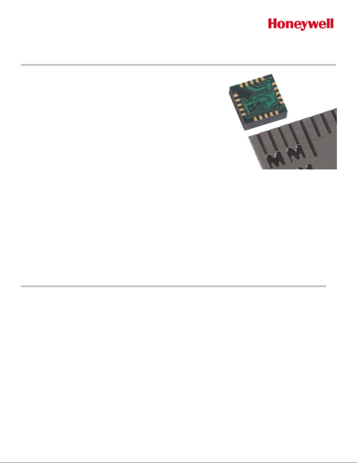
The Honeywell HMC5843 is a surface mount multi-chip module designed
for low field magnetic sensing with a digital interface for applications such
as low cost compassing and magnetometry. The HMC5843 includes our
state of the art 1043 series magneto-resistive sensors plus Honeywell
developed ASIC containing amplifi cation, strap drivers, offset cancellation,
12-bit ADC and an I2C serial bus interface. The HMC5843 is in a 4.0 by 4.0
by 1.3mm surface mount leadless chip carrier (LCC). Applications for the
HMC5843 include Consumer Electronics, Auto Navigation Systems,
Personal Navigation Devices, and Magnetometers.
The HMC5843 utilizes Honeywell’s Anisotropic Magnetoresistive (AMR) technology that provides advantages over other
magnetic sensor technologies. The sensors feature precision in-axis sensitivity and linearity, solid-state construction with
very low cross-axis sensitivity designed to measure both direction and magnitude of Earth’s magnetic fields, from tens of
micro-gauss to 6 gauss. Honeywell’s Magnetic Sensors are among the most sensitive and reliable low-field sensors in the
industry.
Honeywell continues to maintain product excellence and performance by introducing innovative solid-state magnetic
sensor solutions. These are highly reliable, top performance products that are delivered when promised. Honeywell’s
magnetic sensor solutions provide real solutions you can count on.
FEATURES BENEFITS
ASIC in a Single Package
LCC Surface Mount Package
Controller Interface, Plus Two External SMT Capacitors
Offset Compensation
Page 2

HMC5843
www.honeywell.com
SPECIFICATIONS (* Tested at 25°C except stated otherwise. )
Characteristics Conditions* Min Typ Max Units
Power Supply
Supply Voltage AVDD Referenced to AGND
DVDD Referenced to DGND
Current Draw Sleep Mode (dual supplies)
Idle Mode (dual supplies)
Measurement Mode
AVDD = 2.5 volts, DVDD = 1.8 volts
Sleep Mode (single supply)
Idle Mode (single supply)
Measurement Mode
AVDD = 2.5 volts
Performance
Field Range Full scale (FS) – total applied field -4 +4 gauss
Cross-Axis Sensitivity Cross field = 0.5 gauss,
Happlied = ±3 gauss
Disturbing Field Sensitivity starts to degrade.
Use S/R pulse to restore sensitivity.
Max. Exposed Field No perming effect on zero reading 10000 gauss
Measurement Period Output Rate = 50Hz (10Hz typ.) - 10 msec
I2C Address 7-bit address
8-bit read address
8-bit write address
I2C Rate Controlled by I2C Master -10 +10 %
I2C bus pull-up Internal passive resistors 50 kilo-ohms
I2C Hysteresis Hysteresis of Schmitt trigger inputs on SCL
and SDA - Fall (DVDD=1.8V)
Rise (DVDD=1.8V)
Self Test Positive and Negative Bias Mode ±0.55 gauss
Mag Dynamic Range 3-bit gain control ±0.7 ±1.0 ±4.0 gauss
Linearity Full scale input range 0.1 ±% FS
Gain Tolerance All gain/dynamic range settings ±5 %
Bandwidth -3dB point 10 kHz
Resolution AVDD=3.0V, GN 7 milli-gauss
Signal-to Noise Ratio 70 dB
Turn-on Time 200 us
General
ESD Voltage 700 V
Operating Temperature Ambient -30 85 °C
Storage Temperature Ambient, unbiased -40 125 °C
Weight Nominal 50 milli-grams
2.5
1.6
-
-
-
-
-
-
±0.2% %FS/gauss
20 gauss
0x1E
1.8
2.5
240
0.8
110
340
0.9
0x3D
0x3C
0.603
1.108
3.3
2.0
-
-
-
-
-
-
hex
Volts
Volts
Volts
Volts
uA
uA
mA
uA
uA
mA
hex
hex
2
Page 3
HMC5843
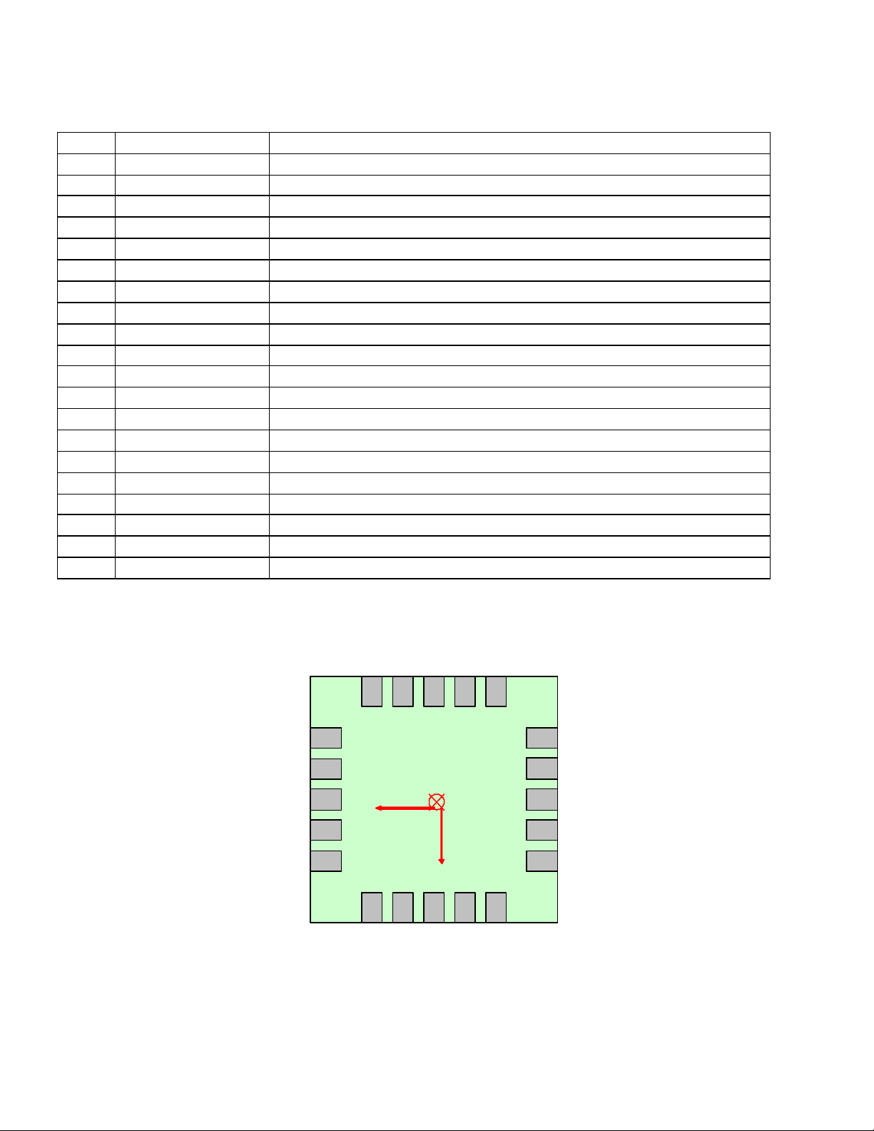
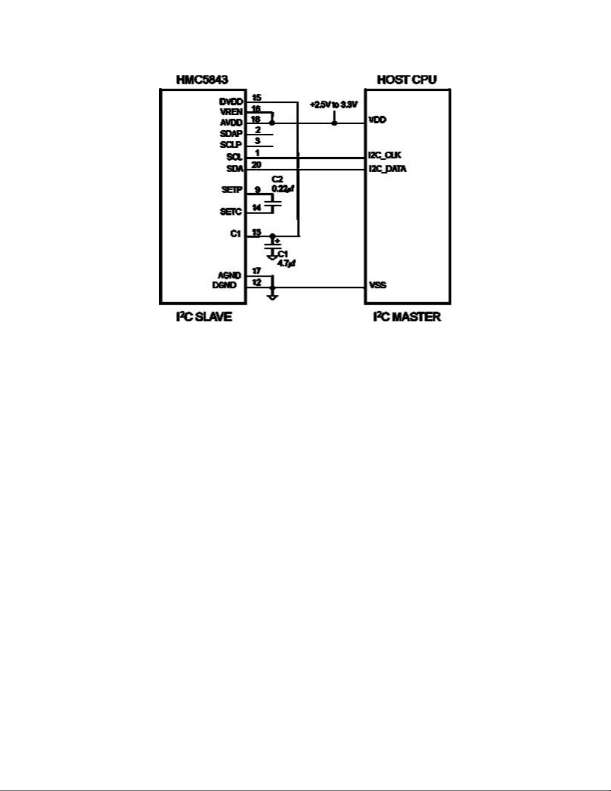
PIN CONFIGURATIONS
(Arrow indicates direction of applied field that generates a positive output voltage after a SET pulse.)
Pin Name Description
1 SCL Serial Clock – I2C Master/Slave Clock
2 SDAP Serial Data Pull-up Resistor – 50k-ohm to VDD
3 SCLP Serial Clock Pull-up Resistor – 50k-ohm to VDD
4 NC No Connection
5 NC No Connection
6 OFFP Offset Strap Positive
7 OFFN Offset Strap Negative
8 NC No Connection
9 SETP Set/Reset Strap Positive – S/R Capacitor (C2) Connection
10 SETN Set/Reset Strap Negative – Test Point
11 SVDD Sensor Supply – Test Point
12 DGND Digital Supply Ground/Return
13 C1 Reservoir Capacitor (C1) Connection
14 SETC S/R Capacitor (C2) Connection – Driver Side
15 DVDD Digital Positive Supply
16 VREN Voltage Regulator Enable, (GND = Dual Supply, AVDD = Single Supply)
17 AGND Analog Supply Ground/Return
18 AVDD Analog Positive Supply
19 DRDY Data Ready – Test Point
20 SDA Serial Data – I2C Master/Slave Data
Table 1: Pin Configurations
20
SDA
20
SDA
DRDY
DRDY
19
19
18
AVDD
18
AVDD
AGND
AGND
17
17
16
VREN
16
VREN
SDAP
SCLP
SDAP
SETC
SETC
SCLP
X
X
C1
C1
TP1
TP1
Z
Z
DGND
DGND
TP0
TP0
1112131415
1112131415
SVDD
SVDD
SCL
SCL
1 2 3 4 5
1 2 3 4 5
Y
Y
DVDD
DVDD
HMC5843 – bottom view
HMC5843 – bottom view
10
10
6
OFFP
6
OFFP
7
OFFN
7
OFFN
8
NC
8
NC
9
SETP
9
SETP
SETN
SETN
www.honeywell.com 3
Page 4
HMC5843
www.honeywell.com
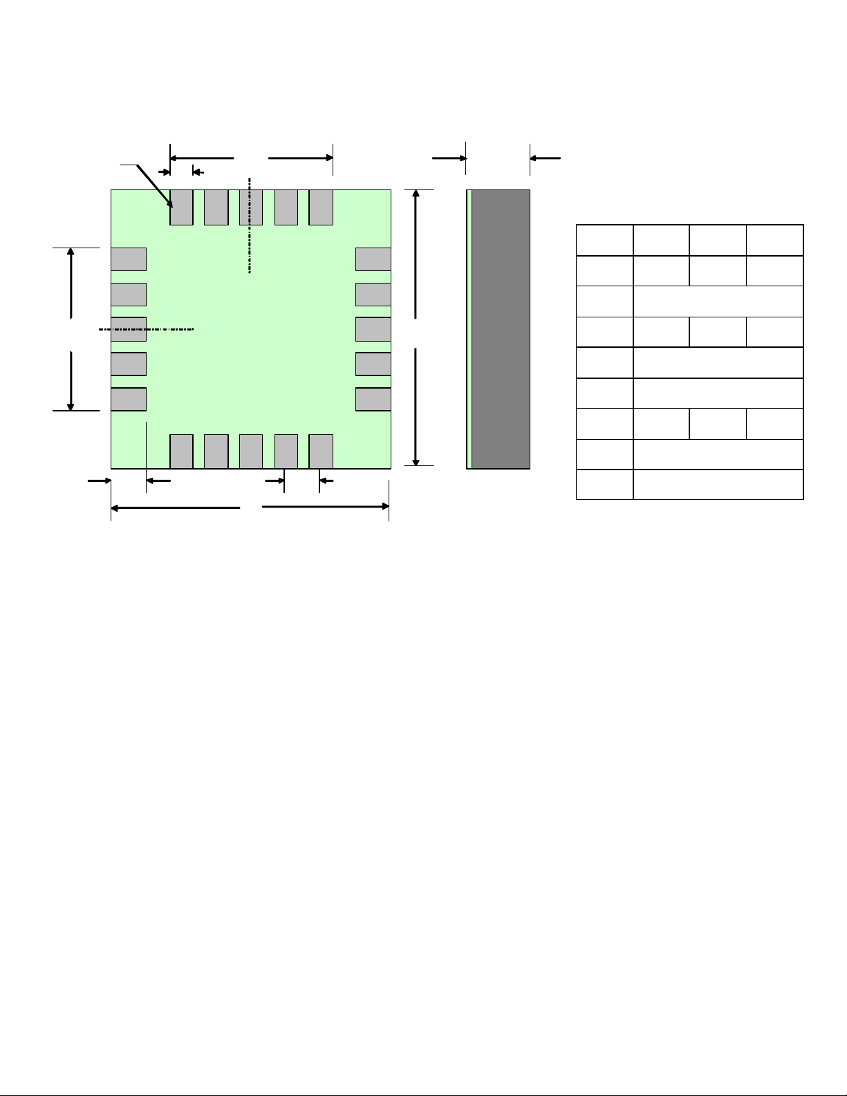
PACKAGE OUTLINES
PACKAGE DRAWING HMC5843 (20-PIN LPCC, dimensions in millimeters)
Pin 1
D2 A
D3
Sym Min Nom Max
A 1.20 - 1.46
D 4.0 BSC
E2
E
L e
D
HMC5843 – bottom view
D2 2.25
D3 0.25 x 20 pins
E 4.0 BSC
E2 2.25
e 0.50 Basic
L 0.40 x 20 pins
MOUNTING CONSIDERATIONS
The following is the recommend printed circuit board (PCB) footprint for the HMC5843.
PCB Pad Definition and Traces
The HMC5843 is a fine pitch LCC package with a 0.50mm pin pitch (spacing), with the pin pads defined as 0. 40mm by
0.25mm in size. PCB pads are recommended to be oversized by 0.025mm from each pad for a short dimension oversize
of 0.05mm. The interior PCB pad is recommended to be 0.05mm oversized per pin with an exterior oversize of 0.20mm
for proper package centering and to permit test probing. Size the traces between the HMC5843 and the external
capacitors (C1 and C2) to handle the 1 ampere peak current pulses with low voltage drop on the traces.
Stencil Design and Solder Paste
A 4 mil stencil and 100% paste coverage is recommended for the electrical contact pads.
Pick and Place
Placement is machine depe ndant and no restrictions are recommended, and have been tested with mechanical centering.
Placement force should be equivalent 1206 SMT resistors and enough force should be used to squeeze the paste out
from the package/contact pad overlap and to keep the package pin contacts vertical.
Reflow and Rework
No special profile is required for the HMC5843 and compatible with lead eutectic and lead-free solder paste reflow
profiles. Honeywell recommends the adherence to solder paste manufacturer’s guidelines. The HMC5843 may be
reworked with soldering irons, but extreme care must be taken not to overheat the copper pads from the part’s fiberglass
substrate. Irons with a tip temperature no greater than 315°C should be used. Excessive rework risks the copper pads
pulling away into the molten solder.
4
Page 5
HMC5843
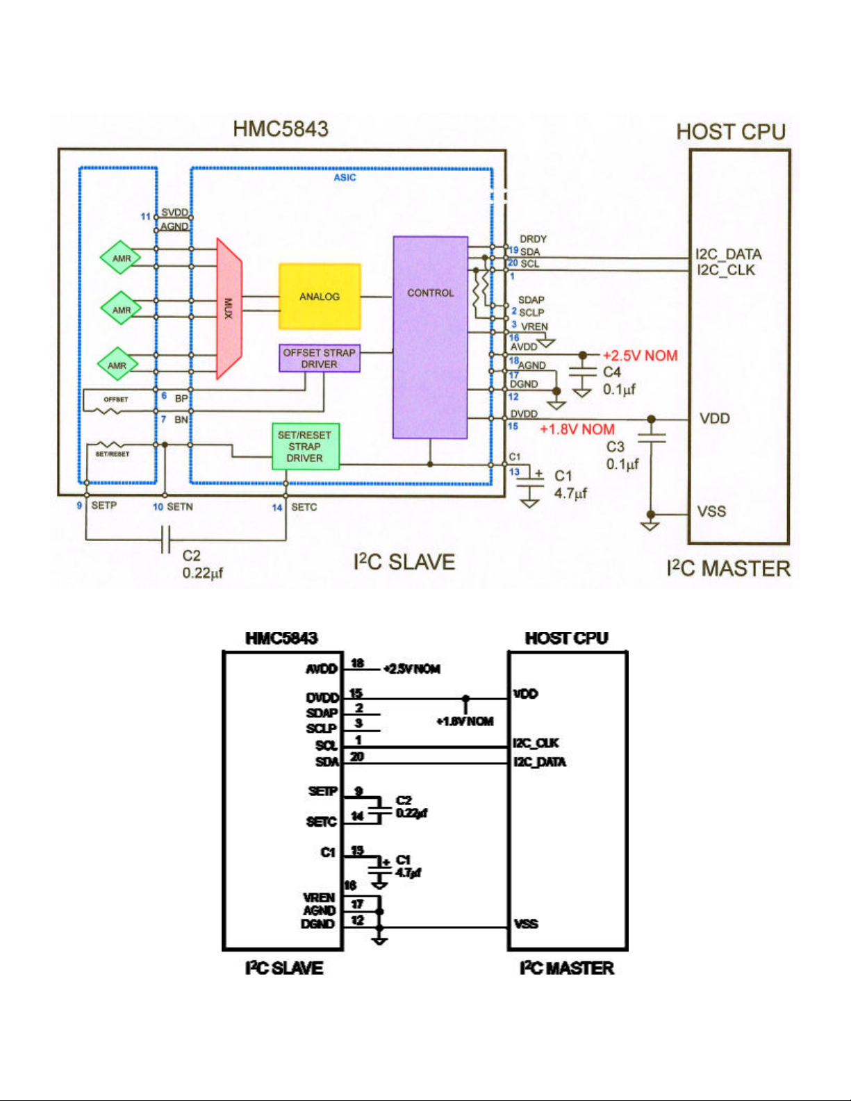
INTERNAL SCHEMATIC DIAGRAM
HMC5843
DUAL SUPPLY REFERENCE DESIGN
www.honeywell.com 5
Page 6
HMC5843
www.honeywell.com
SINGLE SUPPLY REFERENCE DESIGN
BASIC DEVICE OPERATION
Anisotropic Magneto-Resistive Sensors
The Honeywell HMC5843 magnetoresistive sensor circuit is a trio of sensors and application specific support circuits to
measure magnetic fields. With power supply applied, the sensor converts any incident magnetic field in the sensitive axis
directions to a differential voltage output. The magnetoresistive sensors are made of a nickel-iron (Permalloy) thin -film and
patterned as a resistive strip element. In the presence of a magnetic field, a change in the bridge resistive elements
causes a corresponding change in voltage across the bridge outputs.
These resistive elements are aligned together to have a common sensitive axis (indicated by arrows on the pinouts) that
will provide positive voltage change with magnetic fields increasing in the sensitive direction. Because the output only is in
proportion to the one -dimensional axis (the principle of anisotropy) and its magnitude, additional sensor bridges placed at
orthogonal directions permit accurate measurement of arbitrary field direction.
Self Test
An offset strap is designed for self test function. The offset strap measures nominally 13 ohms, and requires 10mA for
each gauss of induced field. The straps will easily handle currents to buck or boost fields through the ±4 gauss linear
measurement range, but designers should note the extreme thermal heating on the sensor die when doing so.
6
Page 7
HMC5843
DVDD
AVDD
Pin
Modes
Description
High High AGND
All, except
Internal voltage regulator: Disabled.
High Low AGND
Idle Internal voltage regulator: Disabled.
Internally
High AVDD
All, except
Internal voltage regulator: Enabled
Low Low -- Off Device in off mode.
Power Management
This device is capable of operating with a single supply (AVDD) or dual supplies (AVDD and DVDD). Pin VREN makes
this selection by enabling the internal digital supply voltage regulator. When VREN is tied to AVDD, the device is in single
supply operation; this device is powered from AVDD; and the internal voltage regulator is enabled. When VREN is tied
to AGND this devices operates with both AVDD and DVDD as supplies. The table below shows the modes available at
the various power supply conditions.
VREN
Supported
Off
regulated
Table 2: Operational Modes and Supply States
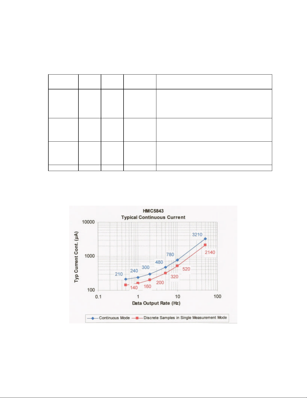
Note the continuous current draw versus data update rate in micro-amperes shown in the graph below. Under 10Hz, the
current stays below 1mA.
Off
Digital I/O pins: Range from DGND to DVDD.
Device fully functional. Digital logic blocks are
powered from DVDD supply, including all onboard clocks.
Digital I/O pins: Range from DGND to DVDD.
Device Measurement functionality not supported.
Device I2C bus and register access supported.
Digital I/O pins: Range from AGND to AVDD
Device fully functional. Digital logic blocks are
powered through on-board regulator.
www.honeywell.com 7
Page 8

HMC5843
www.honeywell.com
Voltage Regulator
This ASIC has an internal voltage regulator which, depending on the application needs, may be used instead of supplying
voltage to pin DVDD. If DVDD pin is used, the internal voltage regulator is not engaged. When both supplies are used,
DVDD is typically high before AVDD, but no latch-up conditions will exist if DVDD is brought high after AVDD.
Power on Reset
Power on reset (POR) circuit shall return the device to the power -on default state. All registers shall be returned to their
default values. Circuitry shall return to it default state, such as, but not limited to: MUX channel, ADC state machine, an d
bias current.
I2C Interface
Control of this device is carried out via the I2C bus. This device will be connected to this bus as a slave device under the
control of a master device, such as the processor.
This device shall be compliant with I2C-Bus Specification, document number: 9398 393 40011. As an I2C compatible
device, this device has a 7-bit serial address and supports I2C protocols. This device shall support standard and fast
modes, 100kHz and 400kHz respectively, but cannot support the high speed mode (Hs). External pull-up resistors are
required to support these standard and fast speed modes. Depending on the application, the internal pull-ups may be
used to support slower data speeds than specified by I2C standards. This device does not contain 50nsec spike
suppression as required by fast mode operation in the I2C-Bus Specification, “Table 4 Characteristics of the SDA and
SCL I/O stages for F/S-mode I2C-bus devices”.
Activities required by the master (register read and write) have priority over internal activities, such as the measurement.
The purpose of this priority is to not keep the master waiting and the I2C bus engaged for longer than necessary .
I2C Pull-up Resistors
Pull-up resistors are placed on the two I2C bus lines. Typically these resistors are off-chip, but, to conserve board space
in specific low clock speed applications, they are internal to this device.
Internal Clock
The device has an internal clock for internal digital logic functions and timing management.
H-Bridge for Set/Reset Strap Drive
The ASIC contains large switching FETs capable of delivering a large but brief pulse to the Set / Reset strap of the
sensor. This strap is largely a resistive load.
8
Page 9

HMC5843
Charge Current Limit
The current that reservoir capacitor (C1) can draw when charging is limited. When using dual supplies this device shall
limit the current drawn from DVDD source to charge this capacitor. When only a single supply is used, Pin DVDD is
externally tied to pin C1. In this configuration, current is still limited. For example, the internal voltage regulator will limit
this current draw.
Bias Current Generator
The bias current generator is used to apply a bias current to the offset strap of the magneto-resistive sensor, which
creates an artificial magnetic field bias on the sensor. This function is enabled and the polarity is set by bits MS[n] in the
configuration register. The bias current generator generates dc current supplied from the AVDD supply.
MODES OF OPERATION
This device has several modes whose primary purpose is power management. This section describes these modes.
Continuous-Measurement Mode
During continuous -measurement mode, the device continuously makes measurements and places measured data in data
output registers. Settings in the configuration register affect the data output rate (bits DO[n]), the measurement
configuration (bits MS[n]), and the gain (bits GN[n]) when in continuous-measurement mode. To conserve current
between measurements, the device is placed in a state similar to idle mode, but the mode is not changed to idle mode.
That is, MD[n] bits are unchanged. Data can be re-read from the data output registers if necessary; however, if the
master does not ensure that the data register is accessed before the completion of the next measurement, the new
measurement may be lost. All registers maintain values while in continuous -measurement mode. The I2C bus is enabled
for use by other devices on the network in while continuous -measurement mode.
Single-Measurement Mode
This is the default single supply power-up mode. In dual supply configuration this is the default mode when AVDD goes
high. During single-measurement mode, the device makes a single measurement and places the measured data in data
output registers. Settings in the configuration register affect the measurement configuration (bits MS[n]), and the gain
(bits GN[n]) when in single-measurement mode. After the measurement is complete and output data registers are
updated, the device is placed sleep mode, and the mode register is changed to sleep mode by setting MD[n] bits. All
registers maintain values while in single -measurement mode. The I2C bus is enabled for use by other devices on the
network while in single -measurement mode.
Idle Mode
During this mode the device is accessible through the I2C bus, but major sources of power consumption are disabled,
such as, but not limited to, the ADC, the amplifier, the SVDD pin, and the sensor bias current. All registers maintain
values while in idle mode. The I2C bus is enabled for use by other devices on the network while in idle mode.
Sleep Mode
This is the default dual supply power-up mode when only DVDD goes high and AVDD remains low. During sleep mode
the device functionality is limited to listening to the I2C bus. The internal clock is not running and register values are not
maintained whil e in sleep mode. The only functionality that exists during this mode is the device is able to recognize and
execute any instructions specific to this device but does not change from sleep mode due to other traffic on the I2C bus.
The I2C bus is enabled for use by other devices on the network while in sleep mode. This mode has two practical
differences from idle mode. First this state will create less noise on system since the clock is disabled, and secondly this
state is a lower current consuming state since the clock is disabled.
Off Mode
During off mode device is off. No device functionality exists. Both AVDD and DVDD are low. The I2C bus is enabled for
use by other devices on the network in off mode. In this mode the I2C pins shall be in a high impedance state.
www.honeywell.com 9
Page 10

HMC5843
www.honeywell.com
01 Configuration Register B
Read/Write
03 D
ata Output X MSB Register
Read
06 Data Output Y LSB Register
Read
08 Data Output Z LSB Register
Read
11 Identification Register B
Read
REGISTERS
This device is controlled and configured via a number of on-chip registers, which are described in this section. In the
following descriptions, set implies a logic 1, and reset or clear implies a logic 0, unless stated otherwise.
Register List
The table below lists the registers and their access. All address locations are 8 bits.
Address Location Name Access
00 Configuration Register A Read/Write
02 Mode Register Read/Write
04 Data Output X LSB Register Read
05 Data Output Y MSB Register Read
07 Data Output Z MSB Register Read
09 Status Register Read
10 Identification Register A Read
12 Identification Register C Read
Table 5: Register List
Register Access
This section describes the process of reading from and writing to this device. The devices uses an address pointer to
indicate which register location is to be read from or written to. These pointer locations are sent from the master to this
slave device and succeed the 7-bit address plus 1 bit read/write identifier.
To minimize the communication between the master and this device, the address pointer updated automatically without
master intervention. This automatic address pointer update has two additional features. First when address 12 or higher
is accessed the pointer updates to address 00 and secondly when address 09 is reached, the pointer rolls back to
address 03. Logically, the address pointer operation functions as shown below.
If (address pointer = 09) then address pointer = 03
Else if (address pointer >= 12) then address pointer = 0
Else (address pointer) = (address pointer) + 1
The address pointer value itself cannot be read via the I2C bus.
Any attempt to read an invalid address location returns 0’s, and any write to an invalid address location or an undefined bit
within a valid address location is ignored by this device.
10
Page 11

HMC5843
0 1 1 5 1 0 0 10 (default)
Configuration Register A
The configuration register is used to configure the device for setting the data output rate and measurement configuration.
CRA0 through CRA7 indicate bit locations, with CRA denoting the bits that are in the configuration register. CRA7 denotes
the first bit of the data stream. The number in parenthesis indicates the default value of that bit.
CRA7 CRA6 CRA5 CRA4 CRA3 CRA2 CRA1 CRA0
(0) (0) (0) DO2 (1) DO1 (0) DO0 (0) MS1 (0) MS0 (0)
Table 6: Configuration Register A
Location Name Description
CRA7 to CRA5 0 These bits must be cleared for correct operation.
CRA4 to CRA2 DO2 to DO0
CRA1 to CRA0 MS1 to MS0
Table 7: Configuration Register A Bit Designations
The Table below shows minimum output data rates given PVT conditions. All three channels shall be measured within a
given data rate.
Data Output Rate Bits. These bits set the rate at which
data is written to all three data output registers.
Measurement Configuration Bits. These bits define the
measurement flow of the device, specifically whether or
not to incorporate an applied bias to the sensor into the
measurement.
DO2 DO1 DO0 Minimum Data Output Rate (Hz)
0 0 0 0.5
0 0 1 1
0 1 0 2
1 0 1 20
1 1 0 50
1 1 1 Not used
Table 8: Data Output Rates
MS1 MS0 Mode
Normal measurement configuration (default). In normal measurement
0 0
0 1
1 0
configuration the device follows normal measurement flow. Pins BP and BN
are left floating and high impedance.
Positive bias configuration. In positive bias configuration, a positive current
is forced across the resistive load on pins BP and BN.
Negative bias configuration. In negative bias configuration, a negative
current is forced across the resistive load on pins BP and BN.
1 1 This configuration is not used.
www.honeywell.com 11
Table 9: Measurement Modes
Page 12

HMC5843
www.honeywell.com
Configuration Register B
The configuration register B for setting the device gain. CRB0 through CRB7 indicate bit locations, with CRB denoting the
bits that are in the configuration register. CRB7 denotes the first bit of the data stream. The number in parenthesis
indicates the default value of that bit.
CRB7 CRB6 CRB5 CRB4 CRB3 CRB2 CRB1 CRB0
GN2 (0) GN1 (0) GN0 (1) (0) (0) (0) (0) (0)
Table 10: Configuration B Register
Location Name Description
Gain Configuration Bits. These bits configure the gain for
CRB7 to CRB5 GN2 to GN0
CRB4 to CRB0 0 This bit must be cleared for correct operation.
Table 11: Configuration Register B Bit Designations
the device. The gain configuration is common for all
channels.
The table below shows nominal gain settings.
GN2 GN1 GN0
0 0 0 ±0.7Ga 1620
0 0 1 ±1.0Ga (default) 1300
0 1 0 ±1.5Ga 970
0 1 1 ±2.0Ga 780
1 0 0 ±3.2Ga 530
1 0 1 ±3.8Ga 460
1 1 0 ±4.5Ga 390
1 1 1
Sensor Input Field
Range:
±6.5Ga
(Not Recommended)
Gain
(counts/
milli-gauss)
280
Output Range
0xF800–0x07FF
(-2048–2047 )
0xF800–0x07FF
(-2048–2047 )
0xF800–0x07FF
(-2048–2047 )
0xF800–0x07FF
(-2048–2047 )
0xF800–0x07FF
(-2048–2047 )
0xF800–0x07FF
(-2048–2047 )
0xF800–0x07FF
(-2048–2047 )
0xF800–0x07FF
(-2048–2047 )
Table 12: Gain Settings
12
Page 13

HMC5843
The resolution of the HMC5843 is based on the gain selection (zero to 7) and the influence of the analog power supply rail
(AVDD). The following graph shows the interaction.
Mode Register
The mode register is an 8-bit register from which data can be read or to which data can be written. This register is used to
select the operating mode of the device. MR0 through MR7 indicate bit locations, with MR denoting the bits that are in the
mode register. MR7 denotes the first bit of the data stream. The number in parenthesis indicates the default value of that
bit.
12
10
8
6
4
Resolution (mGa )
2
HMC5843 Resolution
Gain
0
1
2
3
4
5
6
7
3.23.02.82.62.4
AVDD (V)
MR7 MR6 MR5 MR4 MR3 MR2 MR1 MR0
(0) (0) (0) (0) (0) (0) MD1 (1) MD0 (0)
Table 14: Mode Register
Location Name Description
MR7 to
MR2
MR1 to
MR0
0 These bits must be cleared for correct operation.
MD1 to
MD0
Mode Select Bits. These bits select the operation mode of
this device.
Table 15: Mode Register Bit Designations
www.honeywell.com 13
Page 14

HMC5843
www.honeywell.com
Continuous
-
Conversion Mode. In continuous
-
conversion mode, the
Single
-
Conversion Mode. When
single
-
conversion mode is selected,
MD1 MD0 Mode
device continuously performs conversions an places the result in the
data register. RDY goes high when new data is placed in all three
0 0
0 1
1 0 Idle Mode. Device is placed in idle mode.
1 1 Sleep Mode. Device is placed in sleep mode.
Data Output X Registers A and B
The data output X registers are two 8-bit registers, data output register A and data output register B. These registers
store the measurement result from channel X. Data output X register A contains the MSB from the measurement result,
and data output X register B contains the LSB from the measurement result. The value stored in these two registers is a
16-bit value in 2’s complement form, whose range is 0xF800 to 0x07FF. DXRA0 through DXRA7 and DXRB0 through
DXRB7 indicate bit locations, with DXRA and DXRB denoting the bits that are in the data output X registers. DXRA7 and
DXRB7 denote the first bit of the data stream. The number in parenthesis indicates the default value of that bit.
In the event the ADC reading overflows or underflows for the given channel, or if there is a math overflow during the bias
measurement, this data register will contain the value -4096 in 2’s complement form. This register value will clear when
after the next valid measurement is made.
registers. After a power-on or a write to the mode or configuration
register, the first measurement set is available from all three data
output registers after a period of 2/fDO and subsequent
measurements are available at a frequency of fDO, where fDO is the
frequency of data output.
device performs a single measurement, sets RDY high and returned
to sleep mode. Mode register returns to sleep mode bit values. The
measurement remains in the data output register and RDY remains
high until the data output register is read or another conversion is
performed.
Table 16: Operating Modes
DXRA7 DXRA6 DXRA5 DXRA4 DXRA3 DXRA2 DXRA1 DXRA0
(0) (0) (0) (0) (0) (0) (0) (0)
DXRB7 DXRB6 DXRB5 DXRB4 DXRB3 DXRB2 DXRB1 DXRB0
(0) (0) (0) (0) (0) (0) (0) (0)
Table 17: Data Output X Registers A and B
Data Output Y Registers A and B
The data output Y registers are two 8-bit registers, data output register A and data output register B. These registers
store the measurement result from channel Y. Data output Y register A contains the MSB from the measurement result,
and data output Y register B contains the LSB from the measurement result. The value stored in these two registers is a
16-bit value in 2’s complement form, whose range is 0xF800 to 0x07FF. DYRA0 through DYRA7 and DYRB0 through
DYRB7 indicate bit locations, with DYRA and DYRB denoting the bits that are in the data output Y registers. DYRA7 and
DYRB7 denote the first bit of the data stream. The number in parenthesis indicates the default value of that bit.
In the event the ADC reading overflows or underflows for the given channel, or if there is a math overflow during the bias
measurement, this data register will contain the value -4096 in 2’s complement form. This register value will clear when
after the next valid measurement is made.
14
Page 15

HMC5843
DYRA7 DYRA6 DYRA5 DYRA4 DYRA3 DYRA2 DYRA1 DYRA0
(0) (0) (0) (0) (0) (0) (0) (0)
DYRB7 DYRB6 DYRB5 DYRB4 DYRB3 DYRB2 DYRB1 DYRB0
(0) (0) (0) (0) (0) (0) (0) (0)
Table 18: Data Output Y Registers A and B
Data Output Z Registers A and B
The data output Z registers are two 8-bit registers, data output register A and data output register B. These registers
store the measurement result from channel Z. Data output Z register A contains the MSB from the measurement result,
and data output Z register B contains the LSB from the measurement result. The value stored in these two registers is a
16-bit value in 2’s complement form, whose range is 0xF800 to 0x07FF. DZRA0 through DZRA7 and DZRB0 through
DZRB7 indicate bit locations, with DZRA and DZRB denoting the bits that are in the data output Z registers. DZRA7 and
DZRB7 denote the first bit of the data stream. The number in parenthesis indicates the default value of that bit.
In the event the ADC reading overflows or underflows for the given channel, or if there is a math overflow during the bias
measurement, this data register will contain the value -4096 in 2’s complement form. This register value will clear when
after the next valid measurement is made.
DZRA7 DZRA6 DZRA5 DZRA4 DZRA3 DZRA2 DZRA1 DZRA0
(0) (0) (0) (0) (0) (0) (0) (0)
DZRB7 DZRB6 DZRB5 DZRB4 DZRB3 DZRB2 DZRB1 DZRB0
(0) (0) (0) (0) (0) (0) (0) (0)
Table 19: Data Output Z Registers A and B
Data Output Register Operation
When one or more of the output registers are read, new data cannot be placed in any of the output data registers until all
six data output registers are read. This requirement also impacts DRDY and RDY, which cannot be cleared until new
data is placed in all the output registers.
Status Register
The status register is an 8-bit read-only register. This register is used to indicate device status. SR0 through SR7
indicate bit locations, with SR denoting the bits that are in the status register. SR7 denotes the first bit of the data stream.
SR7 SR6 SR5 SR4 SR3 SR2 SR1 SR0
(0) (0) (0) (0) (0) REN (0) LOCK (0) RDY(0)
Table 20: Status Register
www.honeywell.com 15
Page 16

HMC5843
www.honeywell.com
Ready Bit. Set when data is written to all six data registers.
Location Name Description
SR7 to
SR3
SR2 REN
SR1 LOCK
SR0 RDY
Identification Register A
The identification register A is used to identify the device. IRA0 through IRA7 indicate bit locations, with IRA denoting the
bits that are in the identification register A. IRA7 denotes the first bit of the data stream. The number in parenthesis
indicates the default value of that bit.
The identification value for this device is stored in this register. This is a read-only register.
Register values. ASCII value H
0 These bits must be cleared for correct operation.
Regulator Enabled Bit. This bit is set when the internal
voltage regulator is enabled. This bit is cleared when the
internal regulator is disabled.
Data output register lock. This bit is set when this some but
not all for of the six data output registers have been read.
When this bit is set, the six data output registers are locked
and any new data will not be placed in these register until
on of four conditions are met : one, all six have been read
or the mode changed, two, a POR is issued, three, the
mode is changed, or four, the measurement is changed.
Cleared when device initiates a write to the data output
registers, when in off mode, and after one or more of the
data output registers are written to. When RDY bit is clear
it shall remain cleared for a minimum of 5 µs. DRDY pin
can be used as an alternative to the status register for
monitoring the device for conversion data.
Table 21: Status Register Bit Designations
IRA7 IRA6 IRA5 IRA4 IRA3 IRA2 IRA1 IRA0
0 1 0 0 1 0 0 0
Table 22: Identification Register A Default Values
16
Page 17

HMC5843
Identification Register B
The identification register B is used to identify the device. IRB0 through IRB7 indicate bit locations, with IRB denoting the
bits that are in the identification register A. IRB7 denotes the first bit of the data stream.
Register values. ASCII value 4
Identification Register C
The identification register C is used to identify the device. IRC0 through IRC7 indicate bit locations, with IRC denoting the
bits that are in the identification register A. IRC7 denotes the first bit of the data stream.
Register values. ASCII value 3
IRB7 IRB6 IRB5 IRB4 IRB3 IRB2 IRB1 IRB0
0 0 1 1 0 1 0 0
Table 23: Identification Register B Default Values
IRC7 IRC6 IRC5 IRC4 IRC3 IRC2 IRC1 IRC0
0 0 1 1 0 0 1 1
Table 24: Identification Register C Default Values
www.honeywell.com 17
Page 18

HMC5843
www.honeywell.com
I2C COMMUNICATION PROTOCOL
The HMC5843 communicates via a two -wire I2C bus system as a slave device. The HMC5843 uses a simple protocol
with the interface protocol defined by the I2C bus specification, and by this document . The data rate is at the standard mode 100kbps or 400kbps rates as defined in the I2C Bus Specifications. The bus bit format is an 8-bit Data/Address
send and a 1-bit acknowledge bit. The format of the data bytes (payload) shall be case sensitive ASCII characters or
binary data to the HMC5843 slave, and binary data returned. Negative binary values will be in two’s complement form.
The default (factory) HMC5843 7-bit slave address is 0x3C for write operations, or 0x3D for read operations.
The HMC5843 Serial Clock (SCL) and Serial Data (SDA) lines have optional internal pull-up resistors, but require resistive
pull-ups (Rp) between the master device (usually a host microprocessor) and the HMC5843. Pull-up resistance values of
about 10k ohms are recommended with a nominal 1.8-volt digital supply voltage (DVDD). Other values may be used as
defined in the I2C Bus Specifications or with the internal 50k ohm pull-up resistors (SDAP, SCLP) that can be tied to
DVDD.
The SCL and SDA lines in this bus specification can be connected to a host of devices. The bus can be a single master to
multiple slaves, or it can be a multiple master configuration. All data transfers are initiated by the master device which is
responsible for generating the clock signal, and the data transfers are 8 bit long. All devices are addressed by I2C’s
unique 7 bit address. After each 8-bit transfer, the master device generates a 9 th clock pulse, and releases the SDA line.
The receiving device (addressed slave) will pull the SDA line low to acknowledge (ACK) the successful transfer or leave
the SDA high to negative acknowledge (NACK).
Per the I2C spec, all transitions in the SDA line must occur when SCL is low. This requirement leads to two unique
conditions on the bus associated with the SDA transitions when SCL is high. Master device pulling the SDA line low while
the SCL line is high indicates the Start (S) condition, and the Stop (P) condition is when the SDA line is pulled high while
the SCL line is high. The I2C protocol also allows for the Restart condition in which the master device issues a second
start condition without issuing a stop.
All bus transactions begin with the master device issuing the start sequence followed by the slave address byte. The
address byte contains the slave address; the upper 7 bits (bits7-1), and the Least Significant bit (LSb). The LSb of the
address byte designates if the operation is a read (LSb=1) or a write (LSb=0). At the 9 th clock pulse, the receiving slave
device will issue the ACK (or NACK). Following these bus events, the master will send data bytes for a write operation, or
the slave will clock out data with a read operation. All bus transactions are terminated with the master issuing a stop
sequence.
I2C bus control can be implemented with either hardware logic or in software. Typical hardware designs will release the
SDA and SCL lines as appropriate to allow the slave device to manipulate these lines. In a software implementation, care
must be taken to perform these tasks in code.
OPERATIONAL EXAMPLES
The HMC5843 has a fairly quick stabilization time from no voltage to stable and ready for data retrieval. The nominal 5
milli-seconds with the factory default single measurement mode means that the six Bytes of magnetic data registers
(DXRA, DXRB, DYRA, DYRB, DZRA, and DZRB) are filled with a valid first measurement.
To change the measurement mode to continuous measurement mode, after the 5 milli -second power-up time send the
three bytes:
0x3C 0x02 0x00
This writes the 00 into the second register or mode register to switch from single to continuous measurement mode
setting. With the data rate at the factory default of 10Hz updates (100 milli -seconds interval), a 100 milli-second delay
should be made by the I2C master before querying the HMC5843 data registers for new measurements. To clock out the
new data, send:
0x3D, and clock out DXRA, DXRB, DYRA, DYRB, DZRA, DZRB located in registers 3 through 8. The HMC5843 will
automatically re -point back to register 3 for the next 0x3D query, expected 100 milli-seconds or later.
18
Page 19

HMC5843
Ordering Number
Product
Honeywell
Form #900367
©2009
Honeywell International Inc.
SELF TEST OPERATION
To check the HMC5843 for proper operation, a self test feature in incorporated in which the sensor offset straps are
excited to create a nominal field strength (bias field) to be measured. To implement this self test, the least significant bits
(MS1 and MS0) of configuration register A are changed from 00 to 01 (0x12 or 0b000xxx01). By placing the mode register
into single-conversion mode (0x01), two data acquisition cycles will be made on each magnetic vector. The first
acquisition will be a set pulse followed shortly by measurement data of the external field. The second acquisition will have
the offset strap excited in the positive bias mode (~5.5mA in offset straps) to create about a 0.55 gauss self test field plus
the external field. The first acquisition values will be subtracted from the second acquisition, and the net measurement will
be placed into the data output registers.
If the configuration register B is left at the factory default value of 0x20, values around +715 ADC counts (0.55Ga * 1300
counts/Ga) will be placed in the data output registers. To leave the self test mode, change MS1 and MS0 bit of the
configuration register A back to 0x 00. Also change the mode register if single-conversion mode is not the intended next
mode of operation.
SCALE FACTOR CALIBRATION
Using the method described above in section SELF TEST OPERATION, user can scale sensors’ sensitivity to match each
other. Since placing device in positive bias mode (or alternatively negative bias mode) applies the same artificial field on
all three axis, the resulting ADC measurement in data output registers can be used to scale the sensors.
EXTERNAL CAPACITORS
The two external capacitors should be ceramic type construction with low ESR characteristics. Reservoir capacitor C1 is
nominally 4.7 micro-farads in capacitance, with the set/reset capacitor C2 nominally 0.22 micro-farads in capacitance.
Low ESR characteristics may not be in many smallest size SMT ceramic capacitors (0402), so be prepared to up-size the
capacitors to gain Low ESR characteristics.
ORDERING INFORMATION
HMC5843
HMC5843-TR
HMC5843-demo
HMC5843-eval
3-Axis Digital Compass IC
Tape and Reel 2.5k pieces/reel
Demonstration Kit
Evaluation Board
FIND OUT MORE
For more information on Honeywell’s Magnetic Sensors visit us online at www.honeywell.com/magneticsensors or contact
us at 800-323-8295 (763 -954-2474 internationally).
The application circuits herein constitute typical usage and interface of Honeywell product. Honeywell does not warranty or assume liability of customerdesigned circuits derived from this description or depiction.
Honeywell reserves the right to make changes to improve reliability, function or design. Honeywell does not assume any liability arising out of the
application or use of any product or circuit described herein; neither does it convey any license under its patent rights nor the rights of others.
U.S. Patents 4,441,072, 4,533,872, 4,569,742, 4,681,812, 4,847,584 and 6,529,114 apply to the technology described
12001 Highway 55
Plymouth, MN 55441
Tel: 800-323-8295
www.honeywell.com 19
www.honeywell.com/magneticsensors
February 2009
Page 20

New Products Announcement
New Evaluation & Demonstration Products
Now Available From Honeywell
Effective Tools to Assist Integrating
Honeywell’s Magnetic Sensor Technology
Honeywell has recently added a new line of evaluation and demonstration boards to the magnetic sensor family. These
new products allow engineers to evaluate the products in a pin-out configuration as well as provide necessary
application information such as product schematics. The new products include:
• HMC1042L 2-axis + HMC1041Z 1-axis Demonstration Board
This demonstration board for the 2-axis HMC1042L and 1-axis HMC1041Z provides the sensors
to create 3-axis magnetic sensing prototype with support analog circuitry for earth's magnetic
field detection. Along with the magnetoresistive sensors, three difference amplifier circuits, and
a MOSFET-based set/reset strap driver circuit are included on a 1" by 1" printed circuit board
with two rows of 0.1" spaced pins for solder-less prototyping usage. The difference amplifiers
are set up for high gains with a +/-1 gauss dynamic range. The magnetic XYZ vector outputs are
analog voltages with respect to rail-splitter voltage reference. The set/reset input is 3 volt CMOS
logic levels. Included with this demo are 3 HMC1041Z & 3 HMC1042L samples.
• HMC1043 3-axis Demonstration Board
This demonstration board for the 3-axis HMC1043 provides the sensors to create 3-axis
magnetic sensing prototypes with support analog circuitry for earth's magnetic field detection.
Along with the magnetoresistive sensors, three difference amplifier circuits, and a MOSFETbased set/reset strap driver circuit are included on a 1" by 1" printed circuit board with two
rows of 0.1" spaced pins for solder-less prototyping usage. The difference amplifiers are set up
for high gains with a +/ -1 gauss dynamic range. The magnetic XYZ vector outputs are analog
voltages with respect to rail -splitter voltage reference. The set/reset input is 3 volt CMOS logic
levels. Included with this demo are 3 HMC1043 samples.
• HMC5843 3-axis Compass IC Evaluation Board
The HMC5843 evaluation board for the Compass IC contains the HMC5843 atop a 0.8" by 0.8"
plug-board with wide-DIP spaced (0.6") pins for solder less breadboard compatibility. The
evaluation board also contains the two capacitors and I2C pullup resistors needed for typical
function for the retrieval of the XYZ magnetic field information. Both single and dual supply
configurations of the HMC5843 are supported.
• HMC5843 3-axis Compass IC Demonstration Board
The demonstration board for the 3-axis Compass IC provides the HMC5843 plus serial bus
conversion circuits to convert the I2C data to USB interfacing for personal computers. Includes a
6-foot USB cable, software, user manual & 5 samples of the HMC5843.
Page 21

• HMC6343 3-axis Compass with Algorithms Evaluation Board
The HMC6343 evaluation board for the tilt-compensated digital compass IC contains the
HMC6343 mounted on the 0.8" by 0.8" plug-board with wide-DIP spaced (0.6") pins for
solderless breadboard compatibility. The board also contains the external capacitor and I2C
pullup resistors for typical function of the compass. The board contains the four connections
(VDD, GND, SCL, SDA) plus other breakouts.
• HMC6343 3-axis Compass with Algorithms Demonstration Board
The demonstration board for the 3-axis Compass IC provides the HMC6343 part plus serial bus
conversion circuits to convert the I2C data to USB interfacing to personal computers. This small
printed circuit board comes with a 6-foot USB cable and Windows demonstration software to
provide a user friendly way of viewing compass heading, pitch and roll data n umerically and on
aviation-type displays. Communication can still be enabled with the HMC6343, even without the
provided demonstration software, as long as the developer creates a program to emulate the
I2C data packets. This demonstration board uses the USB power supply from the host computer
(~+5 volts) and a green LED indicates power presence.
HMC1042L and HMC1043 evaluation boards coming soon!
For more information regarding these products and engineering development tools call 1-763-954-2474 or toll free at
1-800-323-8295 or visit the Honeywell web site at www.honeywell.com/magnticsensors. From this Internet location,
visitors can immediately download product specifications and other related product information.
To make purchasing quick and easy, products can be ordered from our on line store at http://shop.ssec.honeywell.com/.
 Loading...