

Page 1

查询hmc1022供应商
SENSOR PRODUCTS
APPLICATIONS
Compassing
Navigation Systems
Attitude Reference
Traffic Detection
Medical Devices
Non-Contact Switch
1- and 2-Axis Magnetic
Sensors
HMC1001 / 1002
HMC1021 / 1022
onfigured as a 4-element
wheatstone bridge, these
C
magnetoresistive sensors
convert magnetic fields to
a differential output volt-
age, capable of sensing
magnetic fields as low as
30 µgauss. These MRs
offer a small, low cost,
high sensitivity and high
reliability solution for low
field magnetic sensing.
Not actual size
FEATURES AND BENEFITS
Wide Field Range Field range up to ±6 gauss, (earth’s field = 0.5 gauss)
Small Package
Solid State These small devices reduce board assembly costs, improve reliability and ruggedness com-
On-Chip Coils Patented on-chip set/reset straps to reduce effects of temperature drift, non-linearity errors and
Cost Effective The sensors were specifically designed to be affordable for high volume OEM applications.
• Designed for 1- and 2-axis to work together to provide 3-axis (x, y, z) sensing
• 1-axis part in an 8-pin SIP or an 8-pin SOIC or a ceramic 8-pin DIP package
• 2-axis part in a 16-pin or 20-pin SOIC package
pared to mechanical fluxgates.
loss of signal output due to the presence of high magnetic fields
Patented on-chip offset straps for elimination of the effects of hard iron distortion
Page 2

LINEAR MAGNETIC FIELD SENSORS
HMC1001/1002 SPECIFICATIONS
Characteristics Conditions* Min Typ Max Unit
Bridge Supply Vbridge referenced to GND 5 12 Volts
Bridge Resistance Bridge current = 10mA 600 850 1200 ohm
Operating Temperature (4) -55 150 °C
Storage T emper ature (4) Unbiased -55 175 °C
Field Range (4) Full scale (FS), total applied field -2 +2 gauss
Linearity Error (4) Best fit straight line ±1 gauss 0.1 0.5 %FS
±2 gauss 1 2
Hysteresis Error (4) 3 sweeps across ±2 gauss 0.05 0.10 %FS
Repeatability Error (4) 3 sweeps across ±2 gauss 0.05 0.10 %FS
S/R Repeatability (1) 10
S/R Repeatability (2) Output variation after alternate S/R pulses 2 100 µV
Bridge Offset Offset = (OUT+) – (OUT-), Field=0 gauss -60 -15 30 mV
after Set pulse, Vbridge=8V
Sensitivity S/R Current = 3A 2.5 3.2 4.0 mV/V/gauss
Noise Density (4) Noise at 1 Hz, Vbridge=5V 29 nV/ Hz
Resolution (4) Bandwidth=10Hz, Vbridge=5V 27 µgauss
Bandwidth (4) Magnetic signal (lower limit = DC) 5 MHz
OFFSET Strap Measured from OFFSET+ to OFFSET- 2.5 3.5 ohm
OFFSET Strap Ω Tempco (4) T
A = -40 to 125° C 0.39 %/° C
OFFSET Field (4) Field applied in sensitive direction 46 51 56 mA/gauss
Set/Reset Strap Measured from S/R+ to S/R- 1.5 1.8 ohm
Set/Reset Current (2) (3) (4) 2 µs current pulse, 1% duty cycle 3.0 3.2 5 Amp
Set/Reset Ω Tempco (4) T
A = -40 to 125° C 0.37 %/° C
Disturbing Field (4) Sensitivity starts to degrade. 3 gauss
Use S/R pulse to restore sensitivity.
Sensitivity Tempco (4) T
A = -40 to 125° C Vbridge=8V -0.32 -0.3 -0.28 %/° C
Ibridge=5mA -0.06
Bridge Offset Tempco (4) T
A = -40 to 125° C no Set/Reset ±0.03 %/° C
Vbridge=5V with Set/Reset ±0.001
Resistance T empco (4) T
A = -40 to 125° C 0.25 %/° C
Cross-Axis Effect (4) Cross field=1gauss no Set/Reset ±3 %FS
(see AN-205) with Set/Reset +0.5
Max. Exposed Field (4) No perming effect on zero reading 10000 gauss
Weight HMC1001 0.14 gram
HMC1002 0.53
(1) VBridge = 4.3V, IS/R = 3.2A, VOUT = VSET – VRESET
(2) If VBridge = 8.0V, IS/R = 2.0A, lower S/R current leads to greater output variation.
(3) Effective current from power supply is less than 1mA.
(4) Not tested in production, guaranteed by characterization.
(*) Tested at 25° C except otherwise stated.
Units: 1 gauss (g) = 1 Oersted (in air), = 79.58 A/m, 1G = 10E-4 Tesla, 1G = 10E5 gamma.
2
Page 3

LINEAR MAGNETIC FIELD SENSORS
HMC1021/1022 SPECIFICATIONS
Characteristic Conditions** Min Typ Max Unit
Bridge Supply Vbridge referenced to GND 5 25 Volts
Bridge Resistance Bridge current = 5mA 800 1100 1300 Ω
Operating Temperature (1) HMC1021S, 1021Z, 1022 -55 150 °C
HMC1021D* - 55 300*
Storage T emper ature (1) Unbiased -55 175 °C
Field Range (1) Full scale (FS), — total applied field -6 +6 gauss
Best fit straight line ±1 gauss 0.05
Linearity Error (1) ±3 gauss 0.4 %FS
±6 gauss 1.6
Hysteresis Error (1) 3 sweeps across ±3 gauss 0.08 %FS
Repeatability Error (1) 3 sweeps across ±3 gauss 0.08 %FS
Bridge Offset Offset = (OUT+) – (OUT-), Field = 0 gauss -10 ±2.5 11.25 mV
After Set pulse, Vbridge=5V
Sensitivity S/R Current = 0.5A 0.8 1.0 1.25 mV/V/gauss
Noise Density (1) Noise at 1Hz, Vbridge=5V 48 nV/√Hz
Resolution (1) Bandwidth=10Hz, Vbridge=5V 85 µgauss
Bandwidth (1) Magnetic signal (lower limit = DC) 5 MHz
OFFSET Strap Measured from OFFSET+ to OFFSET- 38 50 60 Ω
OFFSET Strap Ω Tempco (1) T
A = -40 to 125° C 0.39 %/° C
OFFSET Field (1) Field applied in sensitive direction 4.0 4.6 6.0 mA/gauss
Set/Reset Strap Measured from S/R+ to S/R- 5.5 7.7 9 Ω
Set/Reset Current 2µs current pulse, 1% duty cycle 0.5 0.5 4.0 Amp
Set/Reset Ω Tempco (1) T
A = -40 to 125° C 0.37 %/° C
Disturbing Field (1) Sensitivity starts to degrade. Use S/R 20 gauss
pulse to restore sensitivity.
Sensitivity T empco (1) T
A = -40 to 125° C Vbridge=5V -0.32 -0.3 -0.28 %/° C
Ibridge=5mA -0.06
Bridge Offset Tempco (1) T
A = -40 to 125° C no Set/Reset ±0.05 %/° C
Vbridge=5V with Set/Reset ±0.001
Resistance T empco (1) Vbridge=5V , T
A = –40 to 125° C 0.25 %/° C
Cross-Axis Effect (1) Cross field=1 gauss
(see AN-205) Happlied=±1 gauss +0.3 %FS
Max. Exposed Field (1) No perming effect on zero reading 10000 gauss
Set/Reset (1) S/R current ≥ 0.5 Amps 30 µV
*Please reference data sheet, HTMC1021D for specifications.
(1) Not tested in production, guaranteed by characterization.
Units: 1 gauss (G) = 1 Oersted (in air), 1G = 79.58 A/m,
1G = 10E-4 Tesla, 1G = 10E5 gamma
**Tested at 25° C except otherwise stated.
3
Page 4
LINEAR MAGNETIC FIELD SENSORS
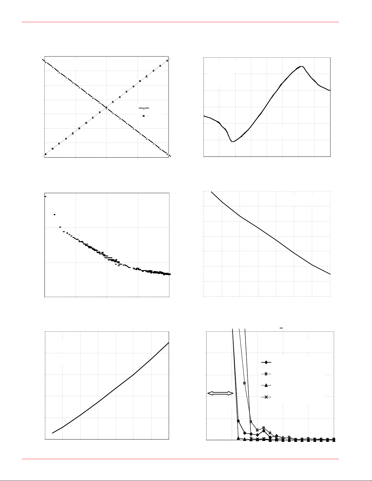
KEY PERFORMANCE DATA
Sensor output vs magnetic field
after being set or reset
1021/1022
Vb=5V
Reset
Set
Voltage Output (mV)
2 sweeps
Output Voltage (mV)
15
10
5
0
-5
-10
-15
Sensor output vs magnetic field
Output is repeatable in field range ±20 Oe
60
1021/1022
40
Vb=5V
20
0
-20
2 sweeps
-40
-20
-2 -1 0 1 2
Field (Oe)
Sensor noise vs frequency
1000
1021/1022
Vb=5V
100
10
Noise Density (nV/rt Hz)
1
0.1 1 10 100 1000
Frequency (Hz)
Bridge resistance vs temperature
1400
All types
1300
Vb=5V
-60
-20 -15 -10 -5 0 5 10 1 5 20
Field (Oe)
Sensitivity vs temperature
1.3
Constant voltage power supply
1021/1022
1.2
1.1
1
0.9
0.8
Sensitivity (mV/V/Oe)
0.7
0.6
-50 -25 0 25 50 75 100 125
Vb=5V
Temperature (C)
Effects of set/reset pulse variation
2µ sec pulse duration, S/R voltage >4V is recommended
1
Vb=5V
1021/1022
0.8
Null Voltage (mV) (Set)
1200
1100
Resistance (ohm)
1000
900
-50 -25 0 25 5 0 75 100 125
Temperature (C)
0.6
0.4
Nonrepeatability
0.2
0
012345
4
no set/reset in
no set/reset in t
region
this region
Null Voltage (mV) (Reset)
Sensitivity (mV/V/Oe) (Set)
Sensitivity (mV/V/Oe) (Reset)
Set/Reset Voltage (V)
Page 5
5
6
7
8
)
)
3
4
5
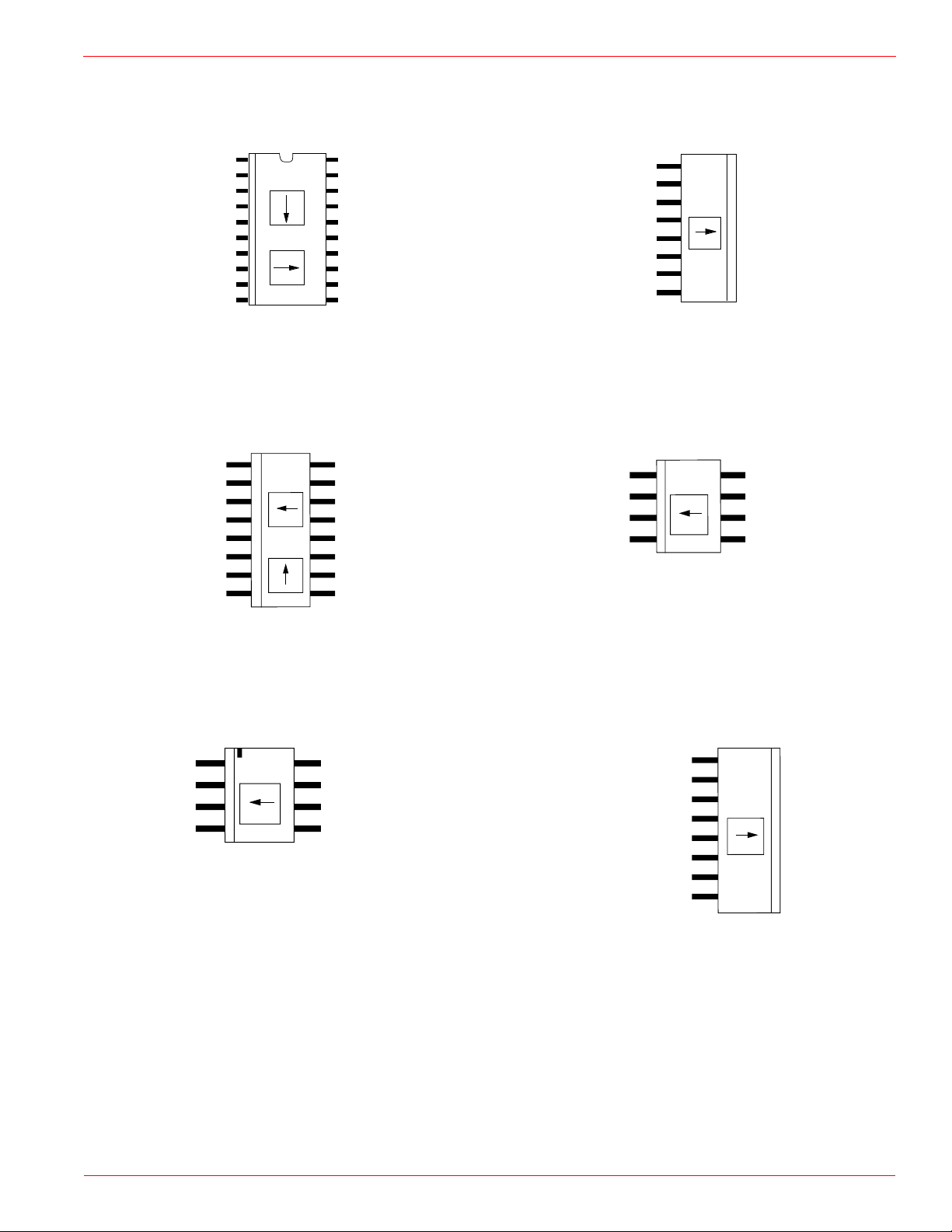
PACKAGE / PINOUT SPECIFICATIONS
LINEAR MAGNETIC FIELD SENSORS
HMC1002—Two-Axis MR Microcircuit
GND1 (A) 1
OUT+ (A) 2
OFFSET- (A) 3
Vbridge (A) 4
OUT- (A)
GND2 (A)
S/R- (B)
GND1 (B)
Out+ (B) 9
OFFSET- (B) 10
Die A
Die B
20 S/R- (A)
19 NC
18 GND PLN
17 OFFSET (+A
16 S/R+ (A)
15 OFFSET+ (B
14 S/R+ (B)
13 GND2 (B)
12 OUT- (B)
11 Vbridge (B)
HMC1022—Two-Axis MR Circuit
OFFSET- (A) 1
OUT+ (A) 2
VBRIDGE (A) 3
OUT- (A) 4
OUT- (B) 5
VBRIDGE (B) 6
GND (A) 7
S/R+ (B) 8
•
Die A
Die B
16 OFFSET+ (A)
15 S/R- (A)
14 S/R+ (A)
13 GND (B)
12 OUT+ (B)
11 OFFSET- (B)
10 OFFSET+ (B)
9 S/R- (B)
HMC1001—One Axis MR Microcircuit
S/R+ 1
OFFSET+ 2
S/RGND
Out+
OFFSET- 6
Vbridge 7
Out- 8
•
Die
HMC1021S—One-Axis MR Circuit
OUT+ 1
VBRIDGE 2
GND 3
OUT- 4
•
Die
HMC1021S
8 OFFSET7 OFFSET+
6 S/R5 S/R+
OUT+ 1
VBRIDGE 2
GND 3
OUT- 4
HMC1021Z—One-Axis MR CircuitHMC1021D—One-Axis MR Circuit
Die
Arrow indicates direction of applied field that generates a
8 OFFSET7 OFFSET+
VBRIDGE 2
6 S/R5 S/R+
OFFSET+ 6
OFFSET- 7
positive output voltage after a SET pulse.
OUT+ 8
OUT- 1
S/R+ 3
GND 4
S/R- 5
•
Die
5
Page 6

LINEAR MAGNETIC FIELD SENSORS
R
BASIC DEVICE OPERATION
Honeywell magnetoresistive sensors are simple resistive
bridge devices (Figure 1) that only require a supply voltage
to measure magnetic fields. When a voltage from 0 to 10
volts is connected to Vbridge, the sensor begins measuring
any ambient, or applied, magnetic field in the sensitive axis.
In addition to the bridge circuit, the sensor has two on-chip
magnetically coupled straps—the OFFSET strap and the
Set/Reset strap. These straps are patented by Honeywell
and eliminate the need for external coils around the devices.
Vbridge
OUT+
(5)
R
=600-1200 Ω
R
(7)
GND
(4)
OFFSET +
R
OUT-
(8)
R
(2)
S/R +
(1)
3.5 Ω max.
Ioffset
2.0 Ω max.
Iset, -Ireset
OFFSET -
(6)
S/R -
(3)
Figure 1—On-Chip components (HMC1001)
Magnetoresistive sensors are made of a nickel-iron
(Permalloy) thin film deposited on a silicon wafer and
patterned as a resistive strip. In the presence of an applied
magnetic field, a change in the bridge resistance causes a
corresponding change in voltage output.
An external magnetic field applied normal to the side of the
film causes the magnetization vector to rotate and change
angle. This in turn will cause the resistance value to vary (∆R/
R) and produce a voltage output change in the Wheatstone
bridge. This change in the Permalloy resistance is termed the
magnetoresistive effect
and is directly related to the angle of
the current flow and the magnetization vector.
During manufacture, the easy axis (preferred direction of
magnetic field) is set to one direction along the length of the
film. This allows the maximum change in resistance for an
applied field within the permalloy film. However, the influence
of a strong magnetic field (more than 10 gauss) along the
easy axis could upset, or flip, the polarity of film
magnetization, thus changing the sensor characteristics.
Following such an upset field, a strong restoring magnetic
field must be applied momentarily to restore, or set, the
sensor characteristics. This effect will be referred to as
applying a set pulse or reset pulse. Polarity of the bridge
output signal depends upon the direction of this internal film
magnetization and is symmetric about the zero field output.
The OFFSET strap allows for several modes of operation
when a dc current is driven through it.
• An unwanted magnetic field can be subtracted out
• The bridge offset can be set to zero
• The bridge output can drive the OFFSET strap to cancel
out the field being measured in a closed loop configuration
• The bridge gain can be auto-calibrated in the system on
command.
The Set/Reset (S/R) strap can be pulsed with a high current to:
• Force the sensor to operate in the high sensitivity mode
• Flip the polarity of the output response curve
• Be cycled during normal operation to improve linearity
and reduce cross-axis effects and temperature effects.
The output response curves shown in Figure 2 illustrate the
effects of the S/R pulse. When a SET current pulse (Iset) is
driven into the SR+ pin, the output response follow the curve
with the positive slope. When a RESET current pulse
(Ireset) is driven into the SR- pin, the output response follow
the curve with the negative slope. These curves are mirror
images about the origin except for two offset effects.
In the vertical direction, the bridge offset shown in Figure 2,
is around -25mV. This is due to the resistor mismatch during
the manufacture process. This offset can be trimmed to zero
by one of several techniques. The most straight forward
technique is to add a shunt (parallel) resistor across one leg
of the bridge to force both outputs to the same voltage. This
must be done in a zero magnetic field environment, usually
in a zero gauss chamber.
The offset of Figure 2 in the horizontal direction is referred to
here as the external offset. This may be due to a nearby ferrous
object or an unwanted magnetic field that is interfering with the
applied field being measured. A dc current in the OFFSET
strap can adjust this offset to zero. Other methods such as
shielding the unwanted field can also be used to zero the
external offset. The output response curves due to the SET
and RESET pulses are reflected about these two offsets.
40
20
0
-20
Vcc=8V
response
after Ireset
(1001/1002)
bridge
offset
response
after Iset
-40
Output Voltage (mV)
-60
-80
-1.50
-1.25
-1.00
external
offset
-0.75
-0.50
Applied Field (Gauss)
-0.25
0.00
0.25
0.50
0.75
1.00
1.25
1.50
Figure 2—Output Voltage vs. Applied Magnetic Field
6
Page 7

NOISE CHARACTERISTICS
LINEAR MAGNETIC FIELD SENSORS
The noise density curve for a typical MR sensor is shown
in Figure 3. The 1/f slope has a corner frequency near 10
Hz and flattens out to 3.8 nV/√Hz. This is approximately
equivalent to the Johnson noise (or white noise) for an
850Ω resistor—the typical bridge resistance. To relate the
noise density voltage in Figure 3 to the magnetic fields, use
the following expressions:
For Vsupply=5V and Sensitivity=3.2mV/V/gauss,
Bridge output response = 16 mV/gauss
or
16 nV/µgauss
The noise density at 1Hz ≈ 30nV/√Hz
and corresponds to 1.8 µgauss/√Hz
For the noise components, use the following expressions:
1/f noise(0.1-10Hz) = 30 * √(ln(10/.1)) nV
64 nV (rms)
4 µgauss (rms)
27 µgauss (p-p)
white noise (BW=1KHz) = 3.8 * √BW nV
120 nV (rms)
50 µgauss (p-p)
1000
Hz)
√
100
(1001/1002)
then it can be compensated for by applying an equal and
opposite field using the OFFSET strap. Another use for the
OFFSET strap would be to drive a current through the strap
that will exactly cancel out the field being measured. This is
called a closed loop configuration where the current feedback
signal is a direct measure of the applied field.
The field offset strap (OFFSET+ and OFFSET-) will generate
a magnetic field in the same direction as the applied field
being measured. This strap provides a 1 Oersted (Oe) field
per 50 mA of current through it in HMC1001/2 and 1 Oe/5mA
in HMC1021/2. (Note: 1 gauss=1 Oersted in air). For
example, if 25 mA were driven from the OFFSET+ pin to the
OFFSET- pin in HMC1001/2, a field of 0.5 gauss would be
added to any ambient field being measured. Also, a current
of -25 mA would subtract 0.5 gauss from the ambient field.
The OFFSET strap looks like as a nominal resistance
between the OFFSET+ and OFFSET- pins.
The OFFSET strap can be used as a feedback element in
a closed loop circuit. Using the OFFSET strap in a current
feedback loop can produce desirable results for measuring
magnetic fields. To do this, connect the output of the bridge
amplifier to a current source that drives the OFFSET strap.
Using high gain and negative feedback in the loop, this will
drive the MR bridge output to zero, (OUT+) = (OUT-). This
method gives extremely good linearity and temperature
characteristics. The idea here is to always operate the MR
bridge in the balanced resistance mode. That is, no matter
what magnetic field is being measured, the current through
the OFFSET strap will cancel it out. The bridge always
“sees” a zero field condition. The resultant current used to
cancel the applied field is a direct measure of that field
strength and can be translated into the field value.
10
Noise Density (nV/
1
0.1 1 10 100 1000
Frequency (Hz)
Figure 3—Typical Noise Density Curve
WHAT IS
OFFSET
STRAP?
Any ambient magnetic field can be canceled by driving a
defined current through the OFFSET strap. This is useful
for eliminating the effects of stray hard iron distortion of the
earth’s magnetic field. For example, reducing the effects of
a car body on the earth’s magnetic field in an automotive
compass application. If the MR sensor has a fixed position
within the automobile, the effect of the car on the earth’s
magnetic field can be approximated as a shift, or offset, in
this field. If this shift in the earth's field can be determined,
The OFFSET strap can also be used to auto-calibrate the
MR bridge while in the application during normal operation.
This is useful for occasionally checking the bridge gain for
that axis or to make adjustments over a large temperature
swing. This can be done during power-up or anytime during
normal operation. The concept is simple; take two point
along a line and determine the slope of that line—the gain.
When the bridge is measuring a steady applied magnetic
field the output will remain constant. Record the reading for
the steady field and call it H1. Now apply a known current
through the OFFSET strap and record that reading as H2.
The current through the OFFSET strap will cause a change
in the field the MR sensor measures—call that delta applied
field (∆Ha). The MR sensor gain is then computed as:
MRgain = (H2-H1) / ∆Ha
There are many other uses for the OFFSET strap than those
described here. The key point is that ambient field and the
OFFSET field simply add to one another and are measured
by the MR sensor as a single field.
7
Page 8

LINEAR MAGNETIC FIELD SENSORS
WHAT IS
SET/RESET
STRAP?
Most low field magnetic sensors will be affected by large
magnetic disturbing fields (>4 - 20 gauss) that may lead to
output signal degradation. In order to reduce this effect, and
maximize the signal output, a magnetic switching technique
can be applied to the MR bridge that eliminates the effect
of past magnetic history. The purpose of the Set/Reset
(S/R) strap is to restore the MR sensor to its high sensitivity
state for measuring magnetic fields. This is done by pulsing
a large current through the S/R strap. The Set/Reset (S/R)
strap looks like a resistance between the SR+ and SR- pins.
This strap differs from the OFFSET strap in that it is
magnetically coupled to the MR sensor in the cross-axis, or
insensitive, direction. Once the sensor is set (or reset), low
noise and high sensitivity field measurement can occur. In
the discussion that follows, the term “set” refers to either a
set or reset current.
When MR sensors exposed to a magnetic disturbing field,
the sensor elements are broken up into ramdonly oriented
magnetic domains (Figure 4A) that leads to sensitivity
degrading. A current pulse (set) with a peak current above
minimum current in spec through the Set/Reset strap will
generate a strong magnetic field that realigns the magnetic
domains in one direction (Figure 4B). This will ensure a high
sensitivity and repeatable reading. A negative pulse (Reset)
will rotate the magnetic domain orientation in the opposite
direction (Figure 4C), and change the polarity of the sensor
outputs. The state of these magnetic domains can retain for
years as long as there is no magnetic disturbing field
present.
Easy Axis
Permalloy (NiFe) Resistor
Magnetization
Random
Domain
Orientations
Fig.4A
After a
Set Pulse
longer, to conserve power. The only requirement is that
each pulse only drive in one direction. That is, if a +3.5 amp
pulse is used to “set” the sensor, the pulse decay should not
drop below zero current. Any undershoot of the current
pulse will tend to “un-set” the sensor and the sensitivity will
not be optimum.
Using the S/R strap, many effects can be eliminated or
reduced that include: temperature drift, non-linearity errors,
cross-axis effects, and loss of signal output due to the
presence of a high magnetic fields. This can be accomplished by the following process:
• A current pulse, Iset, can be driven from the S/R+ to the
S/R- pins to perform a “SET” condition. The bridge output
can then be measured and stored as Vout(set).
• Another pulse of equal and opposite current should be
driven through the S/R pins to perform a "RESET" condition. The bridge output can then be measured and stored
as Vout(reset).
• The bridge output, Vout, can be expressed as: Vout =
[Vout(set) - Vout(reset)]/2. This technique cancels out
offset and temperature effects introduced by the electronics as well as the bridge temperature drift.
There are many ways to design the set/reset pulsing circuit,
though, budgets and ultimate field resolution will determine
which approach will be best for a given application. A simple
set/reset circuit is shown in Figure 5.
6-9V
S/R+
S/R-
0.2µF
3
IRF7105
5,6
7,8
1
25K
4
0.1µF
2
SET RESETRESET
Signal should be in
RESET state when idle
Signal input
5V
Manual Switch
Fig.4B
Magnetization
After a
Reset Pulse
Fig.4C
Figure 4—
The on-chip S/R should be pulsed with a current to realign,
or“flip”, the magnetic domains in the sensor. This pulse can
be as short as two microsecond and on average consumes
less than 1 mA dc when pulsing continuously. The duty
cycle can be selected for a 2 µsec pulse every 50 msec, or
Figure 5—Single-Axis Set/Reset Pulse Circuit (1001)
The magnitude of the set/reset current pulse depends on
the magnetic noise sensitivity of the system. If the minimum
detectable field for a given application is roughly 500
µgauss in HMC1001/2, then a 3 amp pulse (min) is adequate.
If the minimum detectable field is less than 100 µgauss,
then a 4 amp pulse (min) is required. The circuit that
generates the S/R pulse should be located close to the MR
sensor and have good power and ground connections.
The set/reset straps on the Honeywell magnetic sensors
are labeled S/R+ and S/R-. There is no polarity implied
since this is simply a metal strap resistance.
8
Page 9

LINEAR MAGNETIC FIELD SENSORS
V
V
V
S/R
K
F
)25K
HMC
N
(1)T
R
K
F
V
V
V
F*
SHDN
V
GND
C
C
F
Vout
C
C
F*1µF
V
V
MAX
A
*U
V2µF
F
K
K
K
F
S/R
k
F(2)
)
HMC
(1) HEXFET
K
K
F1nF
V74HC
Single Clock Circuitry—
Some form of clock is needed to
trigger the set and reset pulses (Figure 6) to create the
switching signal. The circuit shown in Figure 8 can be used
to create a strong (>4Amp) pulse. The diodes, resistors,
capacitors and inverters basically create the TRS and the
TSR delays. Now a single signal (Clock) can trigger a set or
reset pulse. The minimum timing between the rising and
falling edges of Clock are determined by the 25KΩ and 1nF
time constant. That is, the minimum high and low time for
Clock is ≈25 µs.
Micro Processor—
The circuit in Figure 9 generates a strong
set/reset pulse (>4 Amp) under microprocessor control. The
5
Clock
16
set
TPW ≈ 2 µsec
S/R
reset
-16
Figure 6—Single Clock Set/Reset Timing
SET and RESET signals are generated from a
microprocessor and control the P and N channel HEXFET
drivers (IRF7105). The purpose of creating the TRS and the
TSR delays are to make sure that one HEXFET is off before
the other one turns on. Basically, a break-before-make
switching pattern. The current pulse is drawn from the 4.7
µF capacitor. If the 5V to 20V converter is used as shown in
Figure 7, then the resultant noise and droop on the 16-20V
supply is not an issue. But if the 16-20V supply is used
elsewhere in the system, then a series dropping resistor
(≈500Ω) should be placed between the 4.7µF capacitor and
the supply.
2
0.22µ
5
1
8
7
5
se tantalum capacitors
662
1+
1-
cc
3
2-
2+
1µ
0.22µ
4
6
1N5818
20
1µ
12
Figure 7—5V to 20V Converter
Cloc
SET
RESET
S/R
5
T
RS
T
RS ≥ 5 µsec
T
SR ≥ 5 µsec
T
PW ≈ 2 µsec
+16 to 20V
25
25
0.1µ
3
4
IRF7106 (1)
5,6
7,8
2
1
14
8943
7
1N4001
25
04
1n
25
10
21
2N3904
65
Figure 8—Single Clock Set/Reset Pulse Circuit (1001/1002)
5
T
SR
16
set
10
SET
3904
2
-16
reset
T
PW
RESET
+16 to 20V
25
4
0.1µ
2
4.7µF(3
strap @ 4.5Ω typ.
3A peak (min.)
0.22µ
17
S/R
(2) 0.22µF Tantalum or a
0.68 µF Ceramic CK06
(3) Tantalum, low R
3
5,6
7,8
s with≈0.2ΩRon
4.7µF(1
0.22µ
IRF7106 (2)
S/R
1
antalum,low
(2) HEXFETs with ≈0.2Ω Ron
2003
*
1
strap @ 4.5Ω typ.
3A peak (min.)
2003
1
17
*
•HMC2003 contains one HMC1001 and one HMC1002; together they make the 3-axis sensor.
Three S/R straps are in serial, the total resistance is ~4.5Ω.
Figure 9—Set/Reset Circuit With Microprocessor Control (1001/1002)
9
Page 10

LINEAR MAGNETIC FIELD SENSORS
S/R
K
F
)
HMC
*
(1)T
R
F
F10K
ZTX
ZTX
S/R
K
F
HMC
F
K
ZTX
V
V
Low Field Measurements—
When measuring 100 µgauss
resolution or less, the permalloy film must be completely
set, or reset, to insure low noise and repeatable
measurements. A current pulse of 4 amps, or more, for just
a couple microseconds will ensure this. The circuits in
Figures 8 and 9 are recommended for applications of
HMC1001/2 that require low noise and high sensitivity
magnetic readings.
Low Cost—
For minimum field measurements above 500
µgauss, a less elaborate pulsing circuit can be used. In both
Figures 10 and 11, the pulse signal is switched using lower
cost Darlington transistors and fewer components. This circuit
may have a more limited temperature range depending on the
quality of transistors selected. If accuracy is not an issue and
cost is, then the reset only circuit in Figure 11 will work.
+16 to 20V
0.022µ
0.022µ
Clock
10
4.7µF(1
705
605
0.22µ
strap @ 4.5Ω typ.
3A peak (min.)
17
S/R
antalum,low
2003
1
Figure 10—Single Clock Set/Reset Circuit (1001/1002)
For any magnetic sensor application, if temperature drift is
not an issue, then the reset pulse need only be occasionally
applied. This will save power and enable the use of digital
filtering techniques as shown in Figure 12. Circumstances
for a reset pulse would be 1) power on or, 2) field over/
under range condition. Any other time the sensor should
perform normally.
Clock
+5V
200
0.1µF
0.1µF
0.1µF
0.1µF
10K
10K
1µF (1)
1µF (1)
FMMT717
FMMT617
HMC1022
8
0.1µF
0.1µF
(1) Tantalum, low R
9,1514
Figure 12—5V Circuit for SET/RESET (1021/1022)
The circuit in Figure 13 generates a strong set/reset pulse
under a microprocessor clock driven control. A free running
555 timer can also be used to clock the circuit. The SET
current pulse is drawn from the 1 µF capacitor and a 200
ohm dropping resistor should be placed in series with the
supply to reduce noise.
strap @ 4.5Ω typ.
3A peak (min.)
17
S/R
2003
1
*
Clock
+16 to 20V
100
0.22µ
0.022µ
605
10
5
Clock
S/R
TPW ≈ 2 µsec
reset
-16
*The HMC2003 has 3-axis S/R straps in series.
These are the HMC1001 and HMC1002 sensors.
Figure 11—Single Clock Reset Only Circuit (1001/1002)
10
Page 11

LINEAR MAGNETIC FIELD SENSORS
5V
Clock
+5 to 6V
4 to14V
set
T
PW ~ 2 µsec
S/R
-4 to -14V
reset
Clock
set rst set
Figure 13—Set/Reset Pulse With Clock Control (1021/1022)
Low Power—
For low power application, down to 3.3 volt
supply, the circuit shown in Figure 15 can be used. These
low threshold FETs provide low on-resistance (0.3Ω) at
V
GS=2.7V. The set/reset pulsing does not need to be
continuous. To save power, the SET pulse can be initially
applied followed by a single RESET pulse. The offset (OS)
can be calculated as:
200
4
2
3
5,6
7,8
1
1µF (1)
IRF7105 (2)
DI9952 (2)
(1) Tantalum, low R
(2) Rds ~0.2 ohm
HMC1022
14
0.1µF
SET Pulse
Read Vset
RESET Pulse
Read Vrst
8
9,15
S/R
OS = (Vset + Vrst)/2
This offset term will contain the DC offset of both the sensor
bridge and interface electronics, as well as the temperature
drift of the bridge and interface electronics. Store this value
and subtract it from all future bridge output readings. Once
the bridge is RESET, it will remain in that state for years—
or until a disturbing field (>20 gauss) is applied. A timer can
be set, say every 10 minutes, to periodically update the
offset term. A flow chart is shown in Figure 14 along with a
timing diagram in Figure 15 to illustrate this process.
Reset
Set
Vout
a
T
Vp
TbT
set
a
c
T
d
T
read
Vset
d
T
read
Vrst
OS = (Vset+Vrst)/2
Vout = Vrst - OS
Timer
expired?
n
Read Vrst
y
Figure 14—Low Power Set/Rst Flowchart
+3.3 to
6.5V
Set
200
1,3
2,4
5,6,7,8
5,6,7,8
1µF (1)
+
NDS9933
HMC1022
8
0.1µF
9,1514
S/R
a > 5 µsec
T
b > 1 µsec
T
c > 20 µsec, 50 msec(max)
T
d > 20 µsec Vp > 3 V
T
PW ~ 2 µsec
T
Figure 15—Single Clock Set/Reset Pulse Circuit (1021/1022)
PW
T
reset
-Vp
Reset
2,4
1,3
NDS8926
(1) Tantalum, low R
(2) Rds ~0.2 ohm
S/R
11
Page 12

LINEAR MAGNETIC FIELD SENSORS
*R
Vref
R1*
R2*
K
LM
V
V
Ain+Ai
Ref
Ref
CONV
SCLK
SDATA
NDRDY
XIN
CAL
NCS
V
Gnd
V
V
V
S/R
Vref
K
R3**
K
Gai
F#
R1*
V
V
Calib
LED
*R
Vref
R1*
R2*
K
LM
V
V
Ai
Ai
Ref
Ref
CONV
SCLK
SDATA
NDRDY
XIN
CAL
NCS
V
Gnd
V
V
V
S/R
A
Simple Circuit Application
The circuit in Figure 16 shows a simple application of a
magnetic sensor. This circuit acts as a proximity sensor
and will turn on the LED when a magnet is brought within
0.25 to 0.5 inch of the sensor. The amplifier acts as a
simple comparator and switches low when the HMC1001
bridge output exceeds 30mV. The magnet must be
magnet
movement
Magnetic
Sensor
7
8
5
HMC1001
4
rate:
1. Trim R1 for (+V) - (-V) < 30mV
2. Apply signal < 30mV, LED should be off.
3. Apply signal > 30mV, LED should be on.
+5
100
7
1
+
AMP04
-
8
5
4
* R1 is used to trim switchpoint
# provides 10Hz rolloff
3
V+
2
V-
0.15µ
6
Vout
n=1000,BW=10Hz
+5
400
Figure 16—Magnetic Proximity Switch
+6-15
5 mA
BS250
7
4
Magnetic
Sensor
HMC1001
1.6Ω
13
+
8
5
22.1
100
0.01
10
1
LMC7101
-+
34
strong (200 gauss) and have one of its magnetic poles
point along the sensitive direction of the sensor. This
circuit can be used to detect a door open/closed status or
the presence or absence of an item. Figures 17, 18, 19,
20 and 21 show other circuit examples.
Magnetic
Sensor
7
+5
HMC1001
4
1.6Ω
+
8
5
13
Pulse
650
1.5nF#
1
8
2
-
3
6
+
AMP04
5
+
25
440
2.5V
1 or R2 used to trim offest
# provides 1KHz rolloff
out
CS5509
16 bit A/D
7
n+
8
n-
9
+
10
-
12
6,11,13
+
2
14
15
16
4
3
1
Figure 17—One-Axis Sensor With Digital Interface
650
1.5nF#
1
8
2
-
3
6
+
AMP04
5
+
out
25
440
2.5V
CS5509
16 bit A/D
7
8
n-
9
+
10
-
12
6,11,13
+
2
14
15
16
4
3
1
+5
Serial Bus
Interface
+5
Serial Bus
Interface
1 or R2 used to trim offest
**R3 = 451Ω for 1 axis, 921Ω for 2 axis, or 1411Ω for 3 axis
Pulse
# provides 1KHz rolloff
Figure 18—One-Axis Sensor With Constant Bridge Current and Digital Interface
+5V
10K
4.7uF
tantalum
SW1
1M
OUT-1
V
BRIDGE
S/R+3
GND4
S/R-5
O
FFSET+
FFSET-
O
OUT+8
HMC1021S
+5V
200
2
Sensitive
Direction
6
7
Z
-
MP623
+
+5V
2.5V
LM404-2.5
25K
V+
Vout
Gnd
(1) Momentarily close switch SW1. This creates a SET pulse. (2) Measure bridge output (OUT+) - (OUT-) NOTE: Bridge
output signal will be 5mV/gauss (3) Measure Vout after AD623 amplifier (G~500) NOTE: Vout signal will be 2.5V/gauss
Figure 19—One-Axis Low Cost Sensor
12
Page 13

+5V
+5V
X
1,6
11
Y
8,13
20
14
Magnetic
Magnetic
SensorS
Sensors
4
HMC1002
1.6
1.6
7,18
V+
650
1
R1*
5
2
-
3
2
9
12
16
* R1-R4 used to trim offest
# provides 1KHz rolloff
0.2µF
R2*
V+
R3*
R4*
4.7µF
tantalum
5,6
7,8
2
3
+
5
Vref
650
1
-
+
5
Vref
1K
3
IRF7105
1
8
AMP04
8
AMP04
1.5nF#
6
1.5nF#
6
4
2
LINEAR MAGNETIC FIELD SENSORS
TLC2543
25K
+5V
0.1µF
25K
LM440
2.5V
0.22µF
4.7µF
SR
+
12V
+
12 bit A/D
1
AIN0
2
AIN1
14
Ref+
13
Ref-
10
Gnd
MAX662A
C2-
4
C2+
6
SHDN
Vout
Signal input
5V
Manual Switch
DOUT
NCS
C1+
C1-
Vcc
GND
0.1µF
20
V+
18
CLK
17
DIN
16
15
19
EOC
23
+
0.22µF
1
5
8
7
Signal should be in Rst
state when idle
Set RstRst
+5V
Serial Bus
Interface
+5V
4.7µF
Figure 20—Two-Axis Sensor With Set/Reset Circuit and Digital Interface
+5V
Vb
Vb
Vb
Magnetic
Magnetic
Sensors
Sensor
S/R straps
HMC1001
S/R strap
-
1µF
1 F
LM324a
Vref
NDC7001 or
equiv.
+
Vref
-
+
-
+
0.1µF
0.1 F
0.1µF
0.1 F
-
+
0.1µF
0.1 F
+
LM324b
Vref
+
LM324c
Vref
Vref
+
LM324d
Vref
S/R
100K
100K
0.1uF
Sel1
Sel2
A B
0X
1X
X
2X
3X
4052
200
+5V
Vr ef
+
Output
utp
u
t
O
S/R Control
Figure 21—Three-Axis Low Cost Magnetic Sensor
13
Page 14

LINEAR MAGNETIC FIELD SENSORS
PACKAGE OUTLINES
HMC1002—Package Outline
h
h × 45°
A1
H
A
A
A1
D
20 11
1 10
B
HMC1001—8-Pin SIP and
HMC1021Z—8-Pin SIP
D
HE
1
e B
E
e
8
Symbol
A
A1
B
D
E
e
H
h
Symbol
A
A1
B
D
E
e
H
h
Millimeters Inches
Min
2.489
0.127
0.457
12.675
7.264
1.270 ref
1.270
0.381
Min
1.371
0.101
0.355
9.829
3.810
1.270 ref
5.014
6.850 7.300 0.270 0.287
0.381
Max
2.642
0.279
0.483
12.929
7.417
10.566
ref
Millimeters Inches
Max
1.728
0.249
0.483
11.253
3.988
5.314
0.762
Min
.098
.005
.014
.499
.286
.050 ref
.396
.015
Min
.054
.004
.014
.387
.150
.050 ref
.197
.015
ref
Max
.104
.011
.019
.509
.292
ref
.416
.030
Max
.068
.010
.019
.443
.157
.209
.030
HMC1021D—8-Pin Ceramic DIP
A1
E1
A
Q
D
8 7 6 5
1 2 3 4
L
b
E
e
HMC1021S—8-Pin SOIC
D
E
H
1
A1
A
•
e
HMC1022—16-Pin SOIC
D
H
E
1
•
e
h x 45°
B
916
8
h x 45°
B
A1
Millimeters Inches
—
Min
.054
.004
.014
.189
.150
.229
.015
Min
Max
0.012
0.020
0.405
0.298
0.310
0.060
0.175
Max
.068
.010
.019
.196
.157
.244
.030
Max
.068
.010
.019
.443
.157
.244
.030
Symbol
A
A1
b
D
E
E1
e
Q
L
Symbol
A
A1
B
D
E
e
H
h
Symbol
A
A
A1
B
D
E
e
H
h
Min Max
2.718 ref
7.163
7.366
2.54 ref
3.175
1.270 ref
1.371
0.101
0.355
9.829
3.810
1.270 ref
5.816
0.381
0.305
0.229
0.508
0.406
10.287
—
7.569
7.874
1.524
0.381
4.445
Millimeters Inches
Min
1.371
0.101
0.355
4.800
3.810
5.816
0.381
Min
Max
1.728
0.249
0.483
4.979
3.988
6.198
0.762
Millimeters Inches
Max
1.728
0.249
0.483
11.253
3.988
6.198
0.762
Min
0.107 ref
0.009
0.016
0.282
0.290
0.100 ref
0.015
0.125
.050 ref
.054
.004
.014
.387
.150
.050 ref
.229
.015
14
Page 15

DESIGN / PACKAGE OPTIONS
LINEAR MAGNETIC FIELD SENSORS
Honeywell offers a range of magnetic microcircuit products.
Two different sensor designs and five package
configurations are available:
• HMC1001/1002 series offers a higher sensitivity and
lower field resolution.
• HMC1021/1022 series offers a wider field range, lower
set/reset current and has a lower cost for higher volume
applications.
20/1001CMH22/1201CMHstinU
ytivitisneS1.30.1G/V/Vm
noituloseR7258ssuagµ
egnaR2±6±ssuag
tnerruCtsR/teS0.35.0spmA
tsoCemulovhgihnirewoL
Two-axis parts contain two sensors for the x- and y- field
measurements. Single-axis variations include a SIP package
for mounting through the circuit board to create a 3-axis
solution, a SOIC for direct surface mount, and a ceramic DIP
for high performance military and high temperature
applications.
ORDERING INFORMATION
rebmuNtraPrebmuNsixAytivitisneSelytSegakcaP
1001CMHelgniSG/V/Vm3PISniP-8
2001CMHowTG/V/Vm3CIOSniP-02
D1201CMHelgniSG/V/Vm1PIDcimareCniP-8
Z1201CMHelgniSG/V/Vm1PISniP-8
S1201CMHelgniSG/V/Vm1CIOSniP-8
2201CMHowTG/V/Vm1CIOSniP-61
Solid State Electronics Center • 12001 State Highway 55, Plymouth, MN 55441 • (800) 323-8295 • www.magneticsensors.com
Additional Product Details:
Customer Service Representative
(612) 954-2888 fax: (612) 954-2257
E-Mail: clr@mn14.ssec.honeywell.com
Honeywell reserves the right to make changes to any products or technology herein to improve reliability, function or design. Honeywell does not assume any liability
arising out of the application or use of any product or circuit described herein; neither does it convey any license under its patent rights nor the rights of others.
900248 Rev. B
4-00
15
 Loading...