Honda 08A03-5C4-0500, CX-LH9161B Service Manual
Specification*
ORDER No. 0153
I0
AUTOMOTIVE ELECTRONICS
ACURA
CX-LH9161B
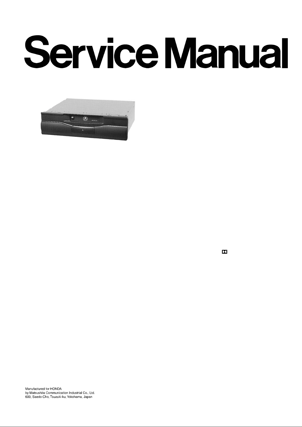
Full-Logic Cassette Tape Player
ACURA PART No. : 08A03-5C4-0500
VEHICLE : ACURA RSX
DESTINATION : Canada
PRODUCED AFTER : Apr., 2001
General
Power Supply DC 12V (11V - 16V),
Test Voltage 13.2V
Negative Ground
Current Consumption Less than 0.8A
Power Output 300mV
Output Impedance 10kΩ
Cassette Player
Reproduction System 4-Track, 2-Program Stereo
Tape Speed 4.76cm/sec.
Wow and Fluter Less than 0.1% (WRMS)
Signal to Noise Ratio 54dB
Dimensions** (W×H×D) 180×50×150mm
Weight** 1.4kg
* Specifications and the design are subject to possible modification
without notice due to improvements.
** Dimensions and Weight shown are approximate.
Doldy noise reduction manufactured under license from Dolby
Laboratories Licensing Corporation.
“Dolby” and the double-D symbol
Laboratories Licensing Corporation.
are trade marks of Dolby
ACURA / CX-LH9161B
CONTENTS
Page Page
1 FEATUERS 2
2 FRONT VIEW
3 REAR VIEW AND CONNECTORS
4 WIRING CONNECTION
5 BLOCK DIAGRAM
6 ALIGNMENT INSTRUCTIONS
7 ALIGNMENT POINTS
8 TERMINALS DESCRIPTION
9 IC BLOCK DIAGRAM 6
2
10 REPLACEM ENT PARTS LIST
11 EXPLODED VIEW (Unit)
2
3
12 TAPE PLAYER PARTS
4
13 EXPLODED VIEW (Tape Deck)
14 WIRING DIAGRAM
5
5
15 SCHEMAT IC DIAGRAM
6
7
9
10
11
12
17
1 FEATUERS
∙
Full Logic control.
∙
Dolby B NR function.
∙
Auto Reverse function.
∙
Repeat Play function.
∙
H-BUS interface.
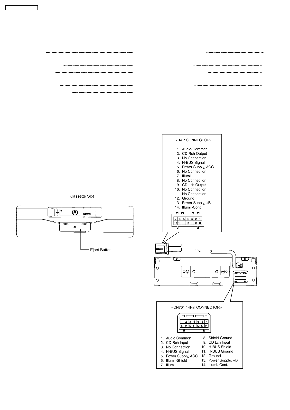
2 FRONT VIEW
3 REAR VIEW AND
CONNECTORS
2
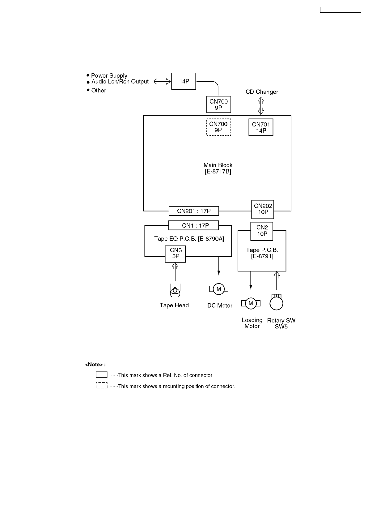
4 WIRING CONNECTION
ACURA / CX-LH9161B
3
ACURA / CX-LH9161B
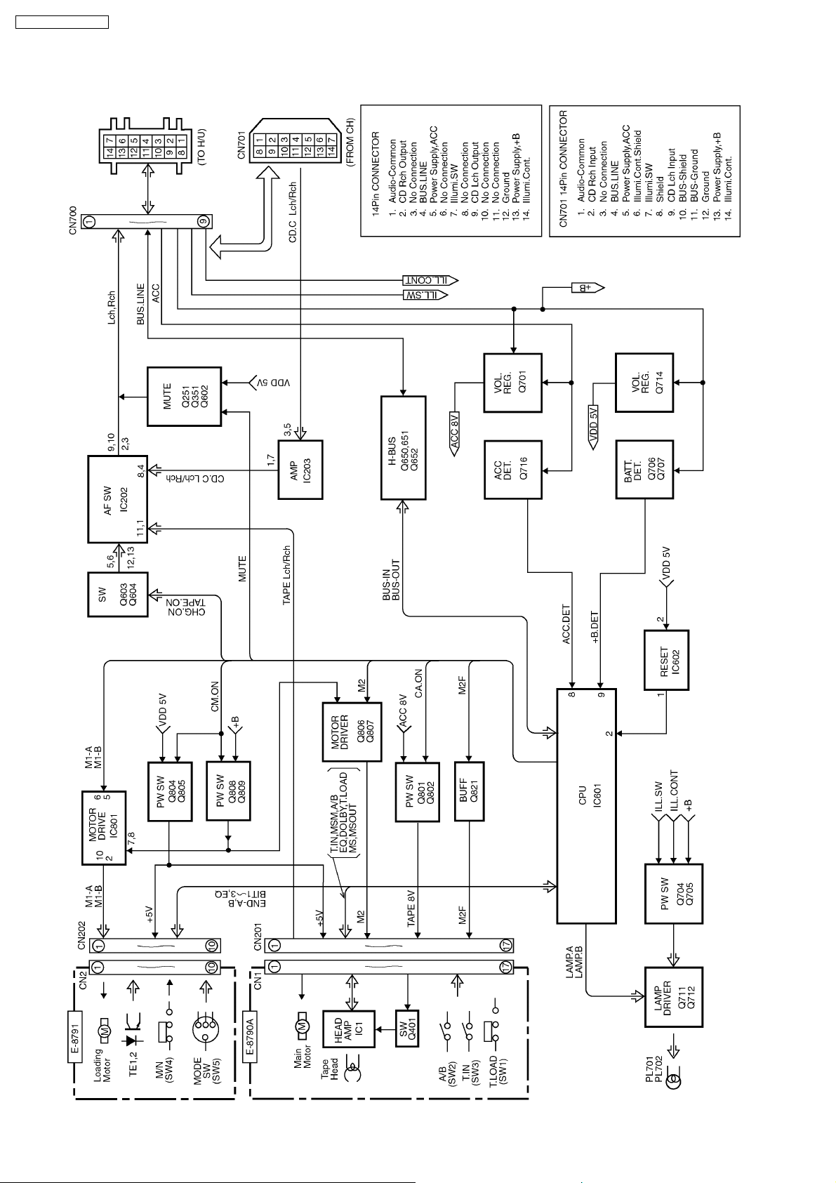
5 BLOCK DIAGRAM
4
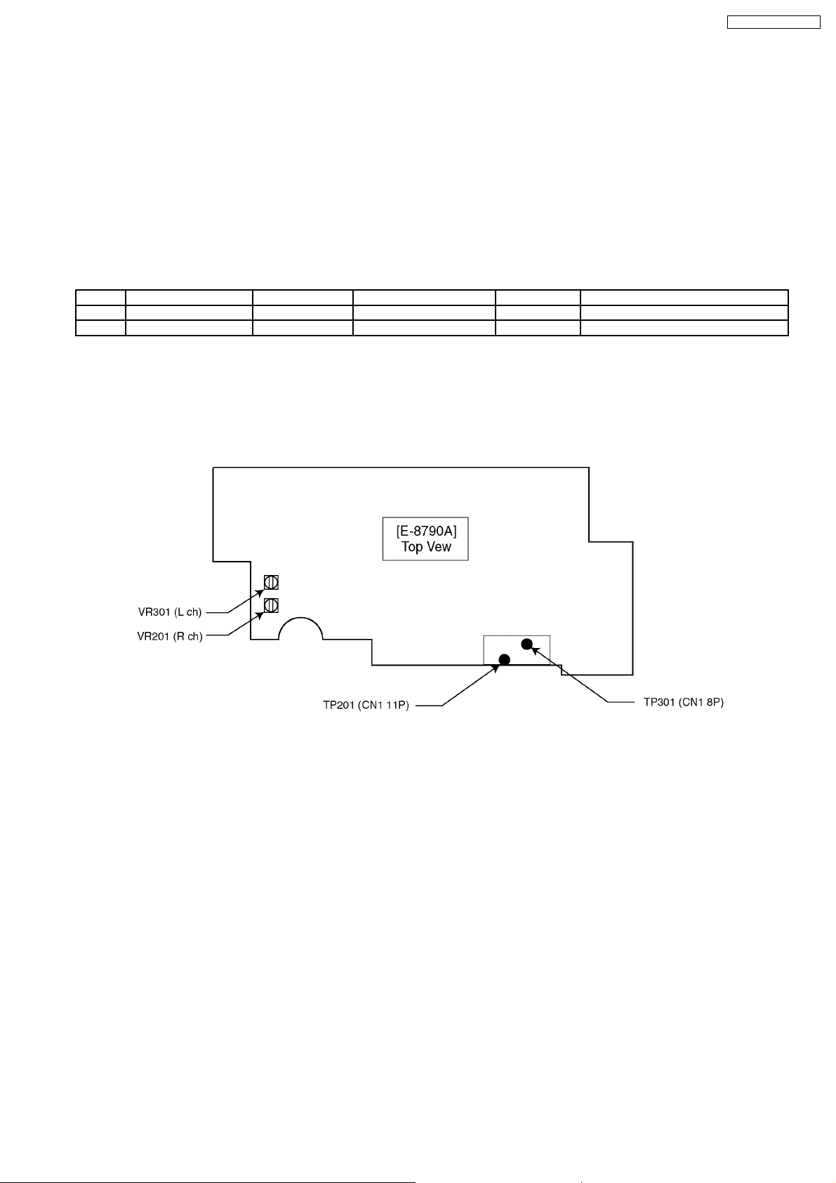
6 ALIGNMENT INSTRUCTIONS
6.1. Alignment Conditions
∙
Power Supply Voltage : DC13.2V
∙
Output Impedance : 10k
Ω
6.2. Dolby NR Alignment
Step Alignment Item Test Tape VTVM Connection Adjust Remarks
(1) DOLBY NR Rch RFKZ0038 TP201 VR201 Adjust for 388mV ±1.0dB
(2) DOLBY NR Lch RFKZ0038 TP301 VR301 Adjust for 388mV ±1.0dB
7 ALIGNMENT POINTS
ACURA / CX-LH9161B
5
ACURA / CX-LH9161B
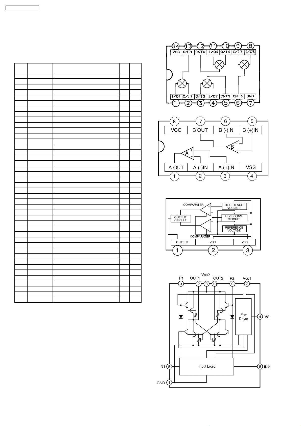
8 TERMINALS
DESCRIPTION
IC601 : C2BBED000014
Pin
No.
1 VDD +5V power supply - 5.6
2 RESET Reset input I 5.6
3 T.LOAD Tape loading detection I 0
4 MS MS mode control O 0
5 DOLBY Dolby control O 0
6 BUS.OUT H-BUS data O 0
7 BUS.IN H-BUS data I 5.4
8 ACC.DET ACC level detection I 0
9 +B.DET Battery level detection I 5.6
10 FLASH.IN Not used I 11 FLASH.OUT Not used - 12 FLASH.CLK Not used - 13 F/R Forward/Reverse control O 0
14 MTL Metal tape selection O 0
15 M2F Tape motor control O 5.6
16 A/B Tape side detection I 0
17 MSM MS gain control O 0
18 T.IN Tape-in switch signal I 0
19 CHG.ON CD changer AF selection O 0
20 TAPE.ON Tape AF selection O 5.6
21 VDD +5V power supply - 5.6
22 VSS Ground - 0
23 MUTE Mute output O 5.6
24 BIT3 Tape mode switch I 0
25 BIT2 Tape mode switch I 5.5
26 END-A Tape end detection I 2.8
27 BIT1 Tape mode switch I 5.5
28 END-B Tape end detection I 1.6
29 EQ Metal tape detection I 0
30 M1-A Tape main motor control O 0
31 M1-B Tape main motor control O 0
32 LAMP.A Pilot lamp on/off O 5.6
33 LAMP.B Pilot lamp on/off O 0
34 EJECT Tape eject switch I 5.6
35 MS.OUT Tape program detection I 0
36 M2 Tape motor control O 5.6
37 CA-ON Tape power control O 5.5
38 CM-ON Tape power control O 5.4
39 IC Not used - 40 X2 Crystal oscillator - 2.8
41 X1 Crystal oscillator - 5.9
42 VSS Ground - 0
Port Description I/O (V)
9 IC BLOCK DIAGRAM
IC202 : YEAMUPD4066C
IC203 : YEAMM5218AP
IC602 : MN1280S
Note :
Voltage measuerments are with respect to ground, with a
voltmeter (Internal resistance : 10M ohms.)
IC801 : YEAMLB1645N
6
 Loading...