


HTG1390
Preliminary
Features
•
Operating voltage: 1.2V ~1.8V
•
7 input lines
•
3 output lines
•
Halt feature reduces power con sumption
•
Up to 16µs instruction cycle with 256kHz
system clock at V
•
All instructions in 1 or 2 machine cycles
•
4K×8 program ROM
•
Data memory RAM size 128×4 bits
General Description
The HTG1390 is the processor from Holtek’s
4-bit stand alone single chip microcontroller
range specifically designed for LCD product applications. The d evice is ide ally s uited for mul -
DD
=1.5V
4-bit Microcontroller
•
27×3 segment LCD driver
•
8-bit table read instruction
•
5 working registers
•
Internal timer overflow interrupt
•
One level subroutine nesting
•
RC oscillator for system clock
•
8-bit timer with internal clo ck source
•
Sound effect circuit
tiple LCD low power applications among which
are calculators, scales, and hand held LCD
products.
1 17th Nov ’98
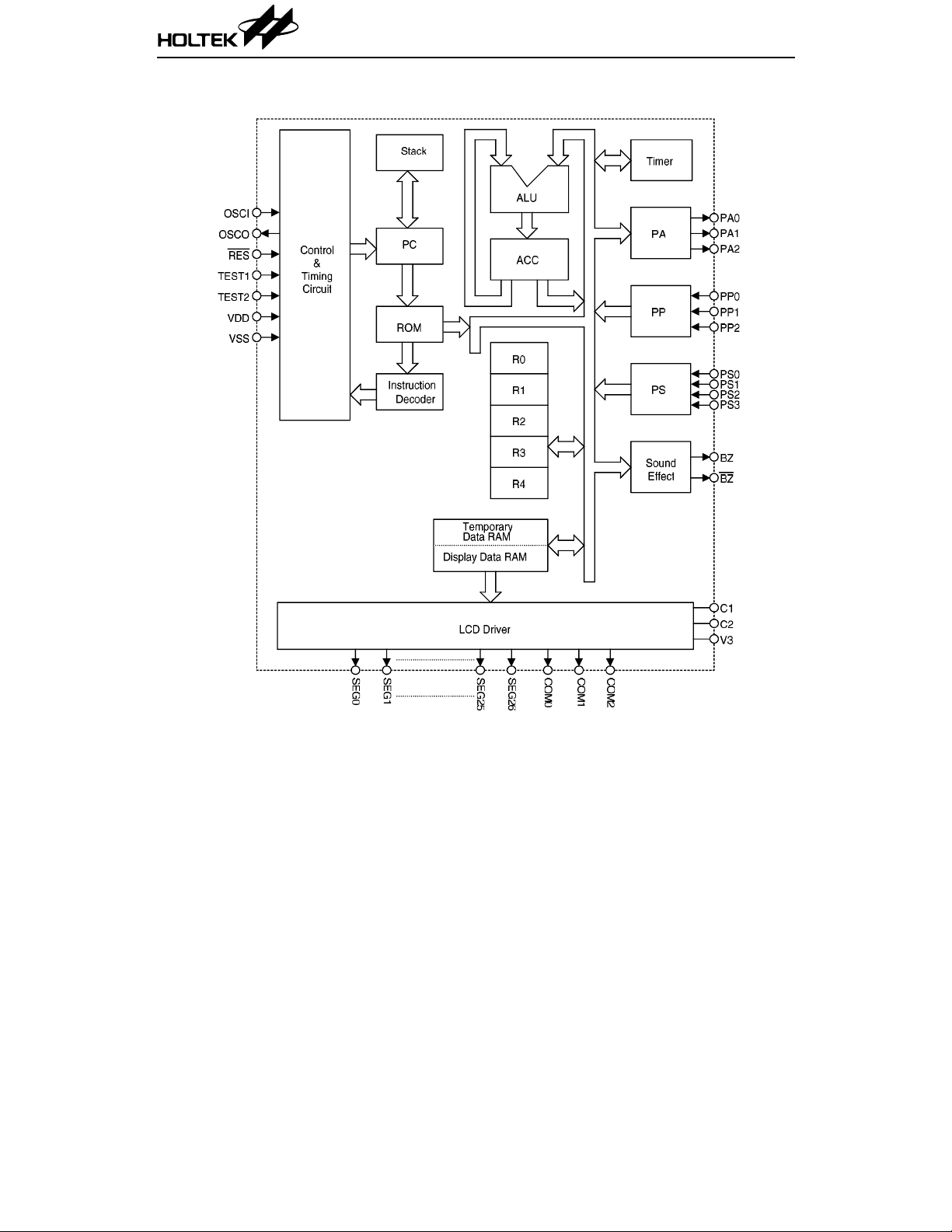
Block Diagram
Preliminary
HTG1390
Notes: ACC: Accumulator
PC: Program counter
R0~R4: Working registers
PA: Output port
PS,PP: Input ports
2 17th Nov ’98
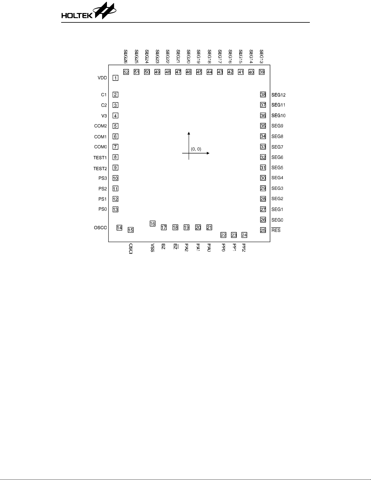
Pad Assignment
Preliminary
HTG1390
Chip size: 1960 × 2300 (µm)
* The IC substrate should be connected to VSS in the PCB layout artwork.
3 17th Nov ’98
2

Preliminary
HTG1390
Pad Coordinates Unit: µm
Pad No. X Y Pad No. X Y
1 –843.74 866.29 27* 853.56 –644.11
2 –843.74 674.39 28* 853.56 –524.11
3* –843.74 554.39 29* 853.56 –404.11
4* –843.74 434.39 30* 853.56 –284.11
5 –843.74 314.39 31* 853.56 –164.11
6 –843.74 194.39 32* 853.56 –44.11
7 –843.74 74.39 33 853.56 75.89
8 –843.74 –45.61 34* 853.56 195.89
9* –843.74 –165.61 35* 853.56 315.89
10* –843.74 –285.61 36* 853.56 435.89
11 –843.74 –405.61 37* 853.56 555.89
12 –843.74 –525.61 38* 853.56 675.89
13 –843.74 –645.61 39* 838.76 935.39
14 –798.04 –856.71 40* 718.76 935.39
15 –668.04 –882.11 41* 598.76 935.39
16 –415.94 –809.01 42* 478.76 935.39
17 –287.94 –853.41 43* 358.76 935.39
18 –154.74 –853.41 44* 238.76 935.39
19* –25.94 –853.41 45* 118.76 935.39
20* 107.26 –853.41 46* –1.24 935.39
21* 236.26 –853.41 47* –121.24 935.39
22* 398.66 –940.91 48* –241.24 935.39
23 518.66 –940.91 49* –361.24 935.39
24 638.66 –940.91 50* –481.24 935.39
25 853.56 –884.11 51* –601.24 935.39
26 853.56 –764.11 52* –721.24 935.39
∗ These pins must be bonded out for functional testing.
4 17th Nov ’98
Preliminary
HTG1390
Pad Description
Pad No. Pad Name I/O Mask Option Function
17, 18 BZ,BZ O Note 1 Sound effect outputs
For test mode only
8
9
5~7 COM2~COM0 O Note 2 Output for LCD panel common plate
10~13 PS3~PS0 I
16 VSS I — Negative power supply, GND
15
14
19~21 PA2~PA0 O
22~24 PP0~PP2 I
25
26~52 SEG0~SEG26 O — LCD driver outputs for LCD panel segment
1 VDD I — Positive power supply
4 V3 I — LCD system power 1/2 bias generated
2, 3 C1, C2 I —
TEST1
TEST2
OSCI
OSCO
RES I —
I
I
Pull-high or
None. Note 3
I
O
NMOS Open
Pull-high or
None. Note 2
—
—
CMOS or
Drain
TEST1 and TEST2 are left open when the
HTG1390 is in normal operation (with an internal
pull high resistor).
4-bit port for input only
OSCI,OSCO are connected to an external resistor
for an internal system clock
3-bit latch port for output only
3-bit port for input only
Input to reset an internal LSI
Reset is active on logical low level
LCD system voltage booster condensor connecting
terminal
Notes: The system clock provides 6 different sources selectable by mask option to drive the sound
effect clock. If the Holtek sound library is used only 128K and 64K are acceptable.
Each bit of ports PS and PP can be a trigger source of the HALT interrupt, selectable by mask
option.
Absolu te Maximu m R a tin g s *
Supply Voltage.................................–0.3V~5.5V Input Voltage.....................VSS–0.3V~VDD+0.3V
Storage Temperature....................–50°C~125°C Operating Temperature......................0°C~70°C
*Note: These are stress ra tings on ly. Stresses exceeding the range specified under “Ab solute Maxi -
mum Ratings” ma y cause substantial damage to the device. Functional operation of this
device at other conditions beyond those listed in the specification is not implied and prolonged
exposure to extreme condition s may affect device reliability.
5 17th Nov ’98
Preliminary
HTG1390
D.C. Characteristics Ta=25°C
Symbol Parameter
V
DD
I
DD
I
STB
V
IL
V
IH
I
OL1
I
OH1
I
OL2
I
OH2
R
PH
Operating Voltage — — 1.2 1.5 1.8 V
Operating Current 1.5V
Standby Current 1.5V
Input Low Voltage 1. 5V — 0 — 0.4 V
Input High Voltage 1.5V — 1.0 — 1.5 V
Port A, BZ & BZ Output Sink
Current
Port A, BZ & BZ Output
Source Current
Segment Output Sink
Current
Segment Output Source
Current
Pull–high Resist an c e 1.5V PS, PP, RES 30 — 300 kΩ
Test Conditions
V
DD
No load,
f
=256kHz
SYS
No load,
HALT mode
VDD=1.5V,
1.5V
V
=0.15V
OL
VDD=1.5V,
1.5V
V
=1.35V
OH
1.5V V
1.5V V
LCD
LCD
Conditions
Min. Typ. Max. Unit
—20—
—— 1 µA
95 100 —
600 700 —
=3V, VOL=0.3V 100 150 — µA
=3V, VOH=2.7V –20 –40 — µA
µA
µA
µA
A.C. Characteristics Ta=25°C
Symbol Parameter
f
SYS
f
LCD
t
COM
t
CY
t
RES
f
SOUND
Notes: * In general, f
System Clock 1.5V R:36kΩ~2MΩ 38 — 400 kHz
LCD Clock 1.5V — — 128* — Hz
LCD Common Period — 1/3 duty — (1/f
Cycle Time — f
Reset Pulse Width — — 5 — — ms
Sound Effect Clock — — —
is selected and optimized by Holtek depending upon f
LCD
Test Conditions
V
DD
Conditions
=256kHz — 16 — µs
SYS
Min. Typ. Max. Unit
)×3— s
LCD
64 or 128
**
SYS
voltage.
** Only these two clocking signal frequencies are supported by the Holtek sound library.
6 17th Nov ’98
— kHz
and the operating
Preliminary
HTG1390
System Architect ure
Program counter – PC
This counter a ddresses the program ROM and
is arranged as an 12-bit binary counter from
PC0 to PC11 whose contents specify a maximum of 4096 addresses. The program counter
counts with an increm ent of 1 or 2 with each
execution of an instruction.
When executing the jump instruction (JMP,
JNZ, JC, JTMR,...), a subroutine call, initial
reset, internal i nterrupt, extern al interrupt or
returning from a subroutine, the program
counter is loaded with the corresponding instruction data as shown in the table.
Notes: P0~P11: Instruction code
@: PC11 keeps current value
S0~S11: Stack register bits
Program memory – ROM
The program memory is the executable memory
and is arranged in a 4096
address is specified by the program counter
(PC). Four special lo cati on s are rese rved as de scribed as follows.
•
Location 0
Activating the pro cessor
first instruction to be fetched from location 0.
•
Location 4
Contains the timer interrupt resulting from a
TIMER overflow . If the interrupts ar e enabled it
causes the program to jump to this s ubroutine.
Mode
Initial reset 0 0 0 0 0 0 0 0 0 0 0 0
Internal interrupt 0 0 0 0 0 0 0 0 0 1 0 0
External interrupt 0 0 0 0 0 0 0 0 1 0 0 0
Jump, call instruction P11 P10 P9 P8 P7 P6 P5 P4 P3 P2 P1 P0
Conditional branch @ P10 P9 P8 P7 P6 P5 P4 P3 P2 P1 P0
Return from subroutine S11 S10 S9 S8 S7 S6 S5 S4 S3 S2 S1 S0
×8 bit format. The
RES pin caus es the
PC1 1 PC10 PC9 PC8 PC7 PC6 PC5 PC4 PC3 PC2 PC1 PC0
•
Location 8
Activating the PS or PP input pins of the
processor with the interrup ts enabled during
Halt mode causes the program to jump to this
location.
•
Locations n00H to nFFH
These are the 256 bytes of each page in pro-
gram memory. This area from n00H to nFFH
and F00H to FFFH can be used as a look–up
table. Instructions such as READ R4A, READ
MR0A, READF R4A, READF MR0A can rea d
the table and transfer the contents of the
table to ACC and R4 or to ACC and a data
memory address specified by the register pair
R1,R0. However as R1,R0 can only store 8
bits, these instructions cannot fully specify
the full 12 bit program m emory address. F or
this reason a jum p instruction should be first
used to place the program counter in the right
page. The above instructions can then be used
to read the look up table data.
Program Counter
Program memory
Program memory
7 17th Nov ’98
Preliminary
HTG1390
Note that the page number n must be greater
than zero as some lo cations in page 0 are reserved for specific usage as mentioned. This
area may functio n as n ormal pro gram m em ory
as required.
The program memory mapping is shown in the
diagram.
In the execution o f an instruction the program
counter is added before the execution phase, so
careful manipulation of READ MR0A and
READ R4A is needed in the page margin.
Stack register
The stack register is a group of registers used to
save the contents of th e program counter (PC)
and is arranged in 13 bits
×1 level. One bit is
used to store the carry flag. An interrupt will
force the contents o f the PC and the carry flag
onto the stack registe r. A subroutine call will
also cause the PC contents to be pushed onto
the stack; however the carry flag will not be
stored. At the end o f a subroutine or a n interrupt (indicated by a retu rn instruction RET or
RETI), the contents of the stack register are
returned to the PC.
Executing “RETI” instruction will restore the
carry flag from st ack r egist er, but “RET” doesn’t.
Working registers – R0,R1,R2,R3,R 4
There are 5 working registers (R0,R1,R2,R3,
R4) usually used to store the frequently accessed intermed iate re su lts . Usin g the instru ctions INC Rn and DEC Rn the working
registers can increment (+1) or decrement (–1).
The JNZ Rn (n=0,1,4) instruction makes efficient use of the working registers as a program
loop counter. Also the register pairs R0,R1 and
R2,R3 are used as a data memory pointer when
the memory transfer instruction is executed.
Data memory – RAM
The static data memory (RAM) is arranged in
256
×4 bit format and is used to store data. All of
the data memory locations are indirectly addressable through the register pair R1,R0 or
R3,R2; for example MOV A,[R3R2] or MOV
[R3R2],A.
There are two areas in the data memory, the
temporary data area and the display data area.
Access to the temporary data area is from 00H
to 7FH. Loca tions E0H to FAH represent the
display data area. The locations between the
temporary and display data areas are undefined and cannot be used .
When data is written into the display data area
it is automatically read by the LCD driver
which then genera tes the corresponding LCD
driving signals.
Data memory
Accumulator – ACC
The accumulator is the most important data
register in the processor. It is one of the sources
of input to the ALU and the destina tion of the
results of the operations performed in the ALU.
Data to and from the I/O ports and memory also
passes through the accumulator.
Arithmetic and logic unit – ALU
This circuit performs the following arithmetic
and logical operations ...
•
Add with or without carry
•
Subtract with or without carry
•
AND, OR, Exclusive-O R
•
Rotate right, left through carry
•
BCD decimal adjust for addition
•
Increment, decrement
•
Data transfers
•
Branch decisions
The ALU not only outputs the results of data
operations, but also sets the status of the carry
flag (CF) in some instructions.
8 17th Nov ’98
Preliminary
HTG1390
Timer
The HTG1390 contains a programmable 8-bit co unt up counter which can be used as a clock to generate
an accurate time base.
The Timer may be set and read with software
instructions and stopped by a hardware reset or
a TIMER OFF instruction. T o restart the timer
load the counter with the value XXH and the n
issue a TIMER ON instruction. Note that XX is
the desired start count imme diate value of the
8 bits. Once the Timer/Counter is started it
increments to a maximum count of FFH and
then overflows to zero (00H). It then continue s
to count until stopped by a TIMER OFF instruction or a reset.
The increment from the maximum count of
FFH to a zero (00H) triggers a timer flag TF and
an internal interrupt request. The interrupt
may be enabled or disabled by executing the EI
and DI instructio n. If the interrupt is ena bled
the timer over flow will cau se a su broutine call
to l ocati on 4 . The state of the timer flag is also
testable with the conditional jump instruction
JTMR. The timer flag is cleared after the interrupt or the JTMR instruction is executed.
If an internal source is used the frequency is
determined by the system clock and the parameter n as defined in the equatio n. The frequency of the internal frequency source can be
selected by mask option.
Frequency of TIMER clock
where n=0,1,2 ...13 selectable by mask option.
Note that n cannot have the value of 6, which is
reserved for internal use .
Interrupt
The HTG1390 provides both internal and external interrupt modes. The DI and EI instructions are used to disable and enable the
interrupts. Durin g Halt mode, if the P P or PS
input pin is triggered on a high to low transition
in the enable interrupt mo de and the program
is not within a CALL subroutin e, the external
interrupt is acti ved. This causes a sub routine
call to location 8 and resets the interrupt latch.
system clock
=
n
2
Likewise when th e timer flag is set in the en able interrupt mode and the program is not
within a CALL subrouti ne the internal interrupt is activated. T his cau ses a su brouti ne cal l
to location 4 and resets the timer flag.
When runni ng un de r a C AL L subrou tin e o r DI
the interrupt acknowle dge is on hold until th e
RET or EI instruction is invoked. The CALL
instruction should no t be used wi thi n an i nte rrupt routine as unpredictable behaviour may
occur. If within a CALL subroutine internal
interrupt occur, the internal interru pt will be
serviced after leaving the CALL subroutine.
The interrupts are disabled by a hardware reset
or a DI instruction. They remain disabled until
the EI instruction is executed.
Each input port pin can be programmed by
mask option to have an external interrupt function in the HALT mode.
Initial reset
The HTG1390 provides an RES pin for system
initialization. Thi s pin is equipp ed with an internal pull high resistor and in combination
with an external 0.1
an internal rese t pulse of sufficient length
guarantee a reset to all intern al circuits. If the
reset pulse is generated externally , the
must be held low for at least 5ms. Normal circuit operation will not commence until the
pin returns high.
The reset performs the following functions:
µ~1µF capacitor, provides
to
RES pin
RES
PC 000H
TIMER Stop
Time flag Reset (Low)
SOUND
Output Port A high (or floating state)
Interrupt Disabled
BZ and
BZ output Low level
Sound off and one sing
mode
9 17th Nov ’98

Preliminary
HTG1390
Halt
This is a special feature of the HTG1390. It will
stop the chip’s normal operation and reduce
power consumption. When the instruction
“HALT” is executed, then
•
The system clock will be stopped
•
The contents of the on-chip RAM and registers remain unchanged
•
LCD segments and commons keep 2VDD voltage (i.e. LCD becomes blank)
The system can escape HALT mode by ways of
initial reset or e xternal interru pt an d wake-up
from the following entry of program counter
value.
•
Initial reset: 000H.
•
Interrupt (enabled): 008H
•
Interrupt (disabled): next address of HALT
instruction.
In HALT mode, each bit of port PS, PP0~PP2,
can be used as externa l interrupt by mask option to wake-up system. This signal is active in
low-going transition.
Sound effects
The HTG1390 includes sound effect circuitry
which offers up to 16 sounds with 3 tone, boom
and noise effects. Holtek supports a sound library which has melodies, alarms, machine
guns etc..
Whenever the instruction “SOUND n” or
“SOUND A” is executed, the specified sound
will begin. Whenever “SOUND OFF” is executed, it terminates the singing sound immediately.
There are two singing modes, SONE mode and
SLOOP mode activated by SOUND ONE and
SOUND LOOP. In SONE mode the specified
sound plays just once. In SLOOP mode the
specified sound keeps re-playing.
Since sounds 0~11 contain 32 notes and sounds
12~15 contain 64 notes the latter possesses better sound than the former.
The frequency of the sound effect circuit can be
selected by mask option.
Frequency of sound effect circuit =
system
2
clock
m
...where m=0,1,2,3,4,5.
Holtek’s sound library supports only sound
clock frequencies of 128K or 64K. To use
Holtek’s sound library the proper system clock
and mask option should be selected.
LCD display memo ry
As mentioned in the data memory se ction the
LCD display memory is embedded in the da ta
memory. It can be read and written to in the
same way as normal data memory.
The figures show the mapping between the display memory and LCD pattern for the
HTG1390.
To turn the display on or o ff a 1/0 is written to
the corresponding bit of the display me mory.
The LCD display module may have any form as
long as the number of commons does not exceed
3 and the numbe r of segme nts do es not exceed
27.
LCD display memory
10 17th Nov ’98

Preliminary
HTG1390
LCD driver output
All LCD segments are random after an initia l
clear. The bias voltage circuits of the LCD display is built-in and no external resistor is
needed.
The output number of the HTG1390 LCD driver
is 27
×3 which can directly drive an LC D with
1/3 duty cycle and 1/2 bias.
The frequency of the LCD driving clock is fixed
at about 128Hz. This is set by Holtek according
to the application and cannot be changed.
LCD driver output
Note: VLCD is produced by double voltage
circuit, therefore its value is double by
VDD.
Oscillator
Only one external resistor is needed for the
HTG1390 oscillator circuit.
The system clock is also used as th e reference
signal of the LCD driving clock, sound effect
clock and internal frequency source of TIMER.
One HTG1390 m achine cycle consists of a sequence of 4 states numbered T1 to T4. Each
state lasts for one oscillator period. The machine cycle is 16
to 256kHz.
µs if the system frequency is up
Interfacing
The HTG1390 microcontroller communicate
with the outside world through 4-bit input port
PS, 3-bit input port PP and one 4-bit output port
PA.
Input ports – PP, PS
All ports can have internal pu ll high resistors
determined by mask option. Every bit of the
input ports PP and P S can b e specifie d to be a
trigger source to wake up the HALT interrupt
by mask option . A high to low transition on one
of these pins will wake up the device from a
HALT status.
Input ports PP and PS
Outpu t port – PA
A mask option is available to select whether the
output is a CMOS or open drain NMOS type.
After an initial clear the output port P A defaults
to be high for CMOS or floating for NMOS.
RC oscillator
Output port PA
11 17th Nov ’98

Preliminary
HTG1390
Mask opt ions
The following either/or options are available by
mask option which the user must select prior to
manufacture.
•
4-bit input ports PP and PS with or without
pull high resistors
•
Each bit of PP and PS can wake up the pro cessor from a HALT state
•
Output Port PA to be CMOS or open drain
NMOS
Application Circuits
•
8-bit programmable timer with external clock
or internal frequency sou rce. Thirteen internal frequency sources are available to provide
an internal clock. Note that a value of n=6
cannot be used for the devices.
•
Six kinds of sound clock frequency:
f
/2m, m=0, 1, 2, 3, 4, 5
SYS
R*: Depends on the required system clock frequency. (R=36kΩ~2MΩ, at VDD=1.5V)
12 17th Nov ’98

Preliminary
Instruction Set Summary
Mnemonic Description Byte Cycle CF
Arithmetic
HTG1390
ADD A,[R1R0]
ADC A,[R1R0]
SUB A,[R1R0]
SBC A,[R1R0]
ADD A,XH
SUB A,XH
DAA
Logic Operation
AND A,[R1R0]
OR A,[R1R0]
XOR A,[R1R0]
AND [R1R0],A
OR [R1R0],A
XOR [R1R0],A
AND A,XH
OR A,XH
XOR A,XH
Increment &
Decrement
INC A
INC Rn
INC [R1R0 ]
INC [R3R2 ]
DEC A
DEC Rn
DEC [R1R0]
DEC [R3R2]
Add data memory to ACC
Add data memory with carry to ACC
Subtract data memory from AC C
Subtract data memory from ACC with borrow
Add immediate data to ACC
Subtract immediate data from ACC
Decimal adjust ACC for addition
AND data memory to ACC
OR data memory to ACC
Exclusive-OR data memory to ACC
AND ACC to data memory
OR ACC to data memory
Exclusive-OR ACC to data memory
AND immediate data to ACC
OR immediate data to ACC
Exclusive-OR immediate data to ACC
Increment ACC
Increment register, n=0~4
Increment data memory
Increment data memory
Decrement ACC
Decrement register, n=0~4
Decrement data memory
Decrement data memory
1
1
1
1
2
2
1
1
1
1
1
1
1
2
2
2
1
1
1
1
1
1
1
1
1
1
1
1
2
2
1
1
1
1
1
1
1
2
2
2
1
1
1
1
1
1
1
1
√
√
√
√
√
√
√
—
—
—
—
—
—
—
—
—
—
—
—
—
—
—
—
—
Data Move
MOV A,Rn
MOV Rn,A
MOV A,[R1R0]
MOV A,[R3R2]
MOV [R1R0],A
MOV [R3R2],A
MOV A,XH
MOV R1R0,XXH
MOV R3R2,XXH
MOV R4,XH
Move register to ACC, n=0~4
Move ACC to register, n=0~4
Move data memory to ACC
Move data memory to ACC
Move ACC to data memory
Move ACC to data memory
Move immediate data to ACC
Move immediate data to R1 and R0
Move immediate data to R3 and R2
Move immediate data to R4
13 17th Nov ’98
1
1
1
1
1
1
1
2
2
2
1
—
1
—
1
—
1
—
1
—
1
—
1
—
2
—
2
—
2
—

Preliminary
HTG1390
Mnemonic Description Byte Cycle CF
Rotate
RL A
RLC A
RR A
RRC A
Input & Output
IN A,Pi
OUT PA,A
Branch
JMP addr
JC addr
JNC addr
JTMR addr
JAn addr
JZ A,addr
JNZ A,addr
JNZ Rn,addr
Subroutine
CALL addr
RET
RETI
Flag
CLC
STC
EI
DI
NOP
Rotate ACC left
Rotate ACC left through the carry
Rotate ACC right
Rotate ACC right through the carry
Input port-i to ACC ,port–i=PS,PP
Output ACC to port-A
Jump unconditionally
Jump on carry=1
Jump on carry=0
Jump on timer overflow
Jump on ACC bit n=1
Jump on ACC is zero
Jump on ACC is not zero
Jump on register Rn not zero, n=0,1,4
Subroutine call
Return from subroutine or interrupt
Return from interrupt service routine
Clear carry flag
Set carry flag
Enable interrupt
Disable interrupt
No operation
1
1
1
1
1
1
2
2
2
2
2
2
2
2
2
1
1
1
1
1
1
1
1
1
1
1
1
1
2
2
2
2
2
2
2
2
2
1
1
1
1
1
1
1
√
√
√
√
—
—
—
—
—
—
—
—
—
—
—
—
√
0
1
—
—
—
Timer
TIMER XXH
TIMER ON
TIMER OFF
MOV A,TMRL
MOV A,TMRH
MOV TMRL,A
MOV TMRH,A
Set 8 bits immediate data to TIMER
Set TIMER start counting
Set TIMER stop counting
Move low nibble of TIMER to ACC
Move high nibble of TIMER to ACC
Move ACC to low nibble of TIMER
Move ACC to hight nibble of TIMER
14 17th Nov ’98
2
1
1
1
1
1
1
2
—
1
—
1
—
1
—
1
—
1
—
1
—

Preliminary
HTG1390
Mnemonic Description Byte Cycle CF
Table Read
READ R4A
READ MR0A
READF R4A
READF MR0A
Sound Control
SOUND n
SOUND A
SOUND ONE
SOUND LOOP
SOUND OFF
Miscellaneous
HALT Enter power down mode 2 2
Read ROM code of current page to R4 & ACC
Read ROM code of current page to M(R1,R0), ACC
Read ROM code of page F to R4 & ACC
Read ROM code of page F to M(R1,R0),ACC
Activate SOUND channel n
Activate SOUND channel with ACC
Turn on SOUND one cycle
Turn on SOUND repeat cycle
Turn off SOUND
1
1
1
1
2
1
1
1
1
2
—
2
—
2
—
2
—
2
—
1
—
1
—
1
—
1
—
—
15 17th Nov ’98

Preliminary
HTG1390
Instruction Definitions
ADC A,[R1R0] Add data memory contents and carry to accumulator
Machine code 0 0 0 0 1 0 0 0
Description The contents of the data me mory addressed by the register p air “R1,R0”
and the carry are added to the accumulator. Carry is affected.
Operation ACC
ADD A,XH Add immediate data to accumulator
Machine code 0 1 0 0 0 0 0 0 0 0 0 0 d d d d
Description The specified data is added to the accumulator. Carry is affected.
Operation ACC
ADD A,[R1R0] Add data memory contents to accumulator
Machine code 0 0 0 0 1 0 0 1
Description The contents of the data me mory addressed by the register p air “R1,R0” is
Operation ACC
AND A,XH Logical AND immediate data to accumulator
Machine code 0 1 0 0 0 0 1 0 0 0 0 0 d d d d
Description Data in the accumulator is logically ANDed with the immediate data speci-
Operation ACC
← ACC+M(R1,R0)+CF
← ACC+XH
added to the accumulator. Carry is affected.
← ACC+M(R1,R0)
fied by the code.
← ACC “AND” XH
AND A,[R1R0] Logical AND accumulator with data memory
Machine code 0 0 0 1 1 0 1 0
Description Data in the accumulator is logically ANDed with the data memory ad-
dressed by the register pair “R1,R0”.
Operation ACC
AND [R1R0],A Logical AND data memory with accumulator
Machine code 0 0 0 1 1 1 0 1
Description Data in the data memory addressed by the register pair “R1,R0” is logi-
Operation M(R1,R0)
← ACC “AND” M(R1,R0)
cally ANDed with the accumulator
← M(R1,R0) “AND” ACC
16 17th Nov ’98

Preliminary
CALL address Subroutine call
Machine code 1 1 1 1 a a a a a a a a a a a a
Description The program counter bits 0~11 are saved in the stack and the specified ad-
dress loaded into the program counter.
Operation Stack
CLC Clear carry flag
Machine code 0 0 1 0 1 0 1 0
Description The carry flag is reset to zero.
Operation CF
DAA Decimal-Adjust accumulator
Machine code 0 0 1 1 0 1 1 0
Description The accumulator value is adjusted to BCD (Binary Code Decimal), if the
Operation If ACC>9 or CF=1 then
← PC+2
PC
← address
← 0
contents of the accumulator is greater than 9 or CF (Carry flag) is one.
ACC
← ACC+6, CF ← 1
else
ACC
← ACC, CF ← CF
HTG1390
DEC A Decrement accumulator
Machine code 0 0 1 1 1 1 1 1
Description Data in the accumulator is decremented by one. Carry flag is not affected.
Operation ACC
DEC Rn Decrement register
Machine code 0 0 0 1 n n n 1
Description Data in the working register “Rn” is decremented by one. Carry flag is not
Operation Rn
DEC [R1R0] Decrement data memory
Machine code 0 0 0 0 1 1 0 1
Description Data in the data memory specified by the register pair “R1,R0” is decre-
Operation M(R1,R0)
← ACC–1
affected.
← Rn–1; Rn=R0,R1,R2,R3,R4, for nnn=0,1,2,3,4
mented by one. Carry flag is not affected.
← M(R1,R0)–1
17 17th Nov ’98

Preliminary
DEC [R3R2] Decrement data memory
Machine code 0 0 0 0 1 1 1 1
Description Data in the data memory specified by the register pair “R3,R2” is decre-
mented by one. Carry flag is not affected.
Operation M(R3,R2)
DI Disable interrupt
Machine code 0 0 1 0 1 1 0 1
Description Internal time-out interrupt and external interrupt are disabled.
EI Enable interrupt
Machine code 0 0 1 0 1 1 0 0
Description Internal time-out interrupt and external interrupt are enabled.
HALT Halt system clock
Machine code 0 0 1 1 0 1 1 1 0 0 1 1 1 1 1 0
Description Turn off system clock, and enter power down mode .
Operation PC
IN A,Pi Input port to accumulator
Machine code PS 0 0 1 1 0 0 1 1
← M(R3,R2)–1
← PC+2
HTG1390
PP 0 0 1 1 0 1 0 0
Description The data on port “Pi” is transferred to the accumulator.
Operation ACC
INC A Increment accumulator
Machine code 0 0 1 1 0 0 0 1
Description Data in the accumulator is incremented by one. Carry flag is not affected.
Operation ACC
INC Rn Increment register
Machine code 0 0 0 1 n n n 0
Description Data in the working register “Rn” is incremented by one. Carry flag is not
Operation Rn
← Pi; Pi=PS or PP
← ACC+1
affected.
← Rn+1; Rn=R0~R4 for nnn=0~4
18 17th Nov ’98

Preliminary
INC [R1R0] Increment data memory
Machine code 0 0 0 0 1 1 0 0
Description Data in the data memory specified by the register pair “R1,R0” is incre-
mented by one. Carry flag is not affected.
Operation M(R1,R0)
INC [R3R2] Increment data memory
Machine code 0 0 0 0 1 1 1 0
Description Data memory specified by the register pair “R3,R2” is incremented by one.
Carry flag is not affacted.
Operation M(R3,R2)
JAn address Jump if accumulator bit n is set
Machine code 1 0 0 n n a a a a a a a a a a a
Description Bits 0~10 of the program counte r are replaced with the directly-specified
address but bit 11 of the program counter is unaffected, if accumulator bit
n is set to one.
Operation PC (bit 0~10)
PC
JC address Jump if carry is set
Machine code 1 1 0 0 0 a a a a a a a a a a a
Description Bits 0~10 of the program counte r are replaced with the directly-specified
address but bit 11 of the program counter is unaffected, if the CF (Carry
flag) is set to one.
Operation PC (bit 0~10)
PC
← M(R1,R0)+1
← M(R3,R2)+1
← address, if ACC bit n=1(n=0~3)
← PC+2, if ACC bit n=0
← address, if CF=1
← PC+2, if CF=0
HTG1390
JMP address Direct jump
Machine code 1 1 1 0 a a a a a a a a a a a a
Description Bits 0~11 of the program counter are replaced with the directly-specified
address.
Operation PC
JNC address Jump if carry is not set
Machine code 1 1 0 0 1 a a a a a a a a a a a
Description Bits 0~10 of the program counte r are replaced with the directly-specified
Operation PC (bit 0~10)
← address
address and bit 11 of the program counter is unaffected, if the CF (Carry
flag) is set to zero.
← address, if CF=0
PC
← PC+2, if CF=1
19 17th Nov ’98

Preliminary
JNZ A,address Jump if accumulator is not zero
Machine code 1 0 1 1 1 a a a a a a a a a a a
Description Bits 0~10 of the program counte r are replaced with the directly-specified
address but bit 11 of the program counter is unaffected, if the accumulator
is not zero.
Operation PC (bit 0~10)
PC
← PC+2, if ACC=0
JNZ Rn,address Jump if register is not zero
Machine code R0 1 0 1 0 0 a a a a a a a a a a a
R1 1 0 1 0 1 a a a a a a a a a a a
R4 1 1 0 1 1 a a a a a a a a a a a
Description Bits 0~10 of the program counte r are replaced with the directly-specified
address but bit 11 of the program counter is unaffected, if the register is
not zero.
Operation PC (bit 0~10)
PC
← PC+2, if Rn=0
JTMR address Jump if time-out
Machine code 1 1 0 1 0 a a a a a a a a a a a
Description Bits 0~10 of the program counte r are replaced with the directly-specified
address but bit 11 of the program counter is unaffected, if the TF (Timer
flag) is set to one.
Operation PC (bit 0~10)
PC
← PC+2, if TF=0
← address, if A CC≠ 0
← address, if Rn≠0; Rn=R0,R1,R4
← address, if TF=1
HTG1390
JZ A,address Jump if accumulator is zero
Machine code 1 0 1 1 0 a a a a a a a a a a a
Description Bits 0~10 of the program counte r are replaced with the directly-specified
address but bit 11 of the program counter is unaffected, if the accumulator
is zero.
Operation PC (bit 0~10)
PC
← PC+2, if ACC≠0
MOV A,Rn Move register to accumulator
Machine code 0 0 1 0 n n n 1
Description Data in the working register “Rn” is moved to the accumulator.
Operation ACC
← Rn; Rn=R0~R4, for nnn=0~4
← address, if ACC=0
20 17th Nov ’98

Preliminary
MOV A,TMRH Move timer high nibble to accumulator
Machine code 0 0 1 1 1 0 1 1
Description The high nibble data of the timer counter is loaded to the accumulator.
Operation ACC
MOV A,TMRL Move timer low nibble to accumulator
Machine code 0 0 1 1 1 0 1 0
Description The low nibble data of the timer counter is loaded to the accumulator.
Operation ACC
MOV A,XH Move immediate data to accumulator
Machine code 0 1 1 1 d d d d
Description The 4-bit data specified by the code is loaded to the accumulator.
Operation ACC
MOV A,[R1R0] Move data memory to accumulator
Machine code 0 0 0 0 0 1 0 0
Description Data in the data memory specified by the register pair “R1,R0” is moved to
Operation ACC
← TIMER (high nibble)
← TIMER (low nibble)
← XH
the accumulator.
← M(R1,R0)
HTG1390
MOV A,[R3R2] Move data memory to accumulator
Machine code 0 0 0 0 0 1 1 0
Description Data in the data memory specified by the register pair “R3,R2” is moved to
the accumulator.
Operation ACC
MOV R1R0,XXH Move immediate data to R1 and R0
Machine code 0 1 0 1 d d d d 0 0 0 0 d d d d
Description The 8-bit data specified by the code is loaded to the working registers R1
Operation R1
MOV R3R2,XXH Move immediate data to R3 and R2
Machine code 0 1 1 0 d d d d 0 0 0 0 d d d d
Description The 8-bit data specified by the code is loaded to the working registers R3
Operation R3
← M(R3,R2)
and R0, the high nibble of the data is loaded to R1, and the low nibble to
R0.
← XH (high nibble)
R0
← XH (low nibble )
and R2, the high nibble of the data is loaded to R3, and the low nibble to
R2.
← XH (high nibble)
R2
← XH (low nibble )
21 17th Nov ’98

Preliminary
MOV R4,XH Move immediate data to R4
Machine code 0 1 0 0 0 1 1 0 0 0 0 0 d d d d
Description The 4-bit data specified by the code is loaded to the working register R4.
Operation R4
MOV Rn,A Move accumulator to register
Machine code 0 0 1 0 n n n 0
Description Data in the accumulator is moved to the working register “Rn”.
Operation Rn
MOV TMRH,A Move accumulator to timer high nibble
Machine code 0 0 1 1 1 1 0 1
Description The contents of the accumulator is loaded to the high nibble of the timer
Operation TIMER(high nibble)
MOV TMRL,A Move accumulator to timer low nibble
Machine code 0 0 1 1 1 1 0 0
Description The contents of the accumulator is loaded to the low nibble of the timer
Operation TIMER(low nibble)
← XH
← ACC; Rn=R0~R4, for nnn=0~ 4
counter.
← ACC
counter.
← ACC
HTG1390
MOV [R1R0],A Move accumulator to data memory
Machine code 0 0 0 0 0 1 0 1
Description Data in the accumulator is moved to the data memory specified by the reg-
ister pair “R1,R0”.
Operation M(R1,R0)
MOV [R3R2],A Move accumulator to data memory
Machine code 0 0 0 0 0 1 1 1
Description Data in the accumulator is moved to the data memory specified by the reg-
ister pair “R3,R2”.
Operation M(R3,R2)
NOP No operation
Machine code 0 0 1 1 1 1 1 0
Description Do nothing, but one instruction cycle is delayed.
← ACC
← ACC
22 17th Nov ’98

Preliminary
OR A,XH Logical OR immediate data to accumulator
Machine code 0 1 0 0 0 1 0 0 0 0 0 0 d d d d
Description Data in the accumulator is logically ORed with the immediate data speci-
fied by the code.
Operation ACC
OR A,[R1R0] Logical OR accumulator with data memory
Machine code 0 0 0 1 1 1 0 0
Description Data in the accumulator is logically ORed with the data memory ad-
Operation ACC
OR [R1R0],A Logically OR data memory with accumulator
Machine code 0 0 0 1 1 1 1 1
Description Data in the data memory addressed by the register pair “R1,R0” is logi-
Operation M(R1,R0)
OUT PA,A Output accumulator data to port A
Machine code 0 0 1 1 0 0 0 0
Description The data in the accumulator is transferred to port P A and latched.
Operation PA
← ACC “OR” XH
dressed by the register pair “R1,R0”.
← ACC “OR” M(R1,R0)
cally ORed with the accumulator.
← M(R1,R0) “ OR” ACC
← ACC
HTG1390
READ MR0A Read ROM code of current page to M(R1,R0) and ACC
Machine code 0 1 0 0 1 1 1 0
Description The 8-bit ROM code (current page) addressed by ACC and R4 is moved to
the data memory M(R1,R0) and the accumulator. The high nibble of the
ROM code is loaded to M(R1,R0) and the low nibble of the ROM code is
loaded to the accumulator. The address of the ROM code is specified as be-
low:
Current page
ACC
→ ROM code address bit 7~4
R4
→ ROM code address bit 3~0
Operation M(R1,R0)
ACC
← ROM code (low nibble)
→ ROM code address bit 11~8
← ROM code (high nibble)
23 17th Nov ’98

Preliminary
READ R4A Read ROM code of current page to R4 and accumulator
Machine code 0 1 0 0 1 1 0 0
Description The 8-bit ROM code (current page) addressed by ACC and M(R1,R0) is
moved to the working register R4 and the accumulator . The high nibble of
the ROM code is loaded to R4 and the low nibble of the ROM code is loaded
to the accumulator. The address of the ROM code is specified as below:
Current page
ACC
→ ROM code address bit 7~4
M(R1,R0)
Operation R4
READF MR0A Read ROM Code of page F to M(R1,R0) and ACC
Machine code 0 1 0 0 1 1 1 1
Description The 8-bit ROM code (page F) addressed by ACC and R4 is moved to the
Operation M(R1,R0)
← ROM code (hig h nibble)
ACC
← ROM code (low nibble)
data memory M(R1,R0) and the accumulator. The high nibble of the ROM
code is loaded to M(R1,R0) and the low nibble of the ROM code is loaded to
the accumulator.
Page F
ACC
→ ROM code address bit 7~4
R4
→ ROM code address bit 3~0
ACC
← low nibble of ROM code (page F)
→ ROM code address bit 11~8
→ ROM code address bit 3~0
→ ROM code address bit 11~8 are “1111”
← high nibble of ROM code (page F)
HTG1390
READF R4A Read ROM code of page F to R4 and accumulator
Machine code 0 1 0 0 1 1 0 1
Description The 8-bit ROM code (page F) addressed by ACC and M(R1,R0) is moved to
the working register R4 and the accumulator. The high nibble of the ROM
code is loaded to R4 and the low nibble of the ROM code is loaded to the ac-
cumulator.
Page F
ACC
M(R1,R0)
Operation R4
ACC
RET Return from subroutine or interrupt
Machine code 0 0 1 0 1 1 1 0
Description The program counter bits 0~11 are restored from the stack.
Operation PC
→ ROM code address bit 11~8 are “1111”
→ ROM code address bit 7~4
→ ROM code address bit 3~0
← high nibble of R OM code (page F)
← low nibble of ROM code (page F)
← Stack
24 17th Nov ’98

Preliminary
RETI Return from interrupt subroutine
Machine code 0 0 1 0 1 1 1 1
Decription The program counter bits 0~11 are restored from the stack. The carry flag
before entering the interrupt service routine is restored.
Operation PC
RL A Rotate accumulator left
Machine code 0 0 0 0 0 0 0 1
Description The contents of the accumulator are rotated left one bit. Bit 3 is rotated to
Operation An+1
RLC A Rotate accumulator left through carry
Machine code 0 0 0 0 0 0 1 1
Description The contents of the accumulator are rotated left one bit. Bit 3 replaces the
Operation An+1
← Stack
CF
← CF (before interrupt service routine)
both bit 0 and the carry flag.
← An, An: accumulator bit n (n=0,1,2)
A0
← A3
CF
← A3
carry bit, which is rotated into the bit 0 position.
← An, An: Accumulator bit n (n=0,1,2)
A0
← CF
CF
← A3
HTG1390
RR A Rotate accumulator right
Machine code 0 0 0 0 0 0 0 0
Description The contents of the accumulator are rotated right one bit. Bit 0 is rotated
to both bit 3 and the carry flag.
Operation An
RRC A Rotate accumulator right through carry
Machine code 0 0 0 0 0 0 1 0
Description The contents of the accumulator are rotated right one bit. Bit 0 replaces
Operation An
← An+1, An: Accumulator bit n (n=0,1,2)
A3
← A0
CF
← A0
the carry bit, which bit is rotated into the bit 3 position.
← An+1, An: Accumulator bit n (n=0,1,2)
A3
← CF
CF
← A0
25 17th Nov ’98

Preliminary
SBC A,[R1R0] Subtract data memory contents and carry from ACC
Machine code 0 0 0 0 1 0 1 0
Description The contents of the data me mory addressed by the register p air “R1,R0”
and the complement of the carry are subtracted from the accumulator.
Carry is set if a borrow does not take place in subtraction; otherwise carry
is cleared.
Operation ACC
SOUND A Activate SOUND channel with accumulator
Machine code 0 1 0 0 1 0 1 1
Description The activated sound begins playing in accord ance with the contents of accu-
SOUND LOOP Turn on sound repeat cycle
Machine code 0 1 0 0 1 0 0 1
Description The activated sound plays repeatedly.
SOUND OFF Turn off sound
Machine code 0 1 0 0 1 0 1 0
Description The activated sound will terminate immediately.
← ACC+M(R1,R0)+CF
mulator when the specified sound channel is matched.
HTG1390
SOUND ONE Turn on sound one cycle
Machine code 0 1 0 0 1 0 0 0
Description The activated sound plays once.
SOUND n Activate SOUND channel n
Machine code 0 1 0 0 0 1 0 1 0 0 0 0 n n n n
Description The specified sound begins playing and overwrites the previous activated
sound. (nnnn=0~15)
STC Set carry flag
Machine code 0 0 1 0 1 0 1 1
Description The carry flag is set to one.
Operation CF
SUB A,XH Subtract immediate data from accumulator
Machine code 0 1 0 0 0 0 0 1 0 0 0 0 d d d d
Description The specified data is subtracted from the accumulator . Carry is set if a bor-
Operation ACC
← 1
row does not take place in subtraction; otherwise carry is cleared.
← ACC+XH+1
26 17th Nov ’98

Preliminary
SUB A,[R1R0] Subtract data memory contents from accumulator
Machine code 0 0 0 0 1 0 1 1
Description The contents of the data me mory addressed by the register p air “R1,R0” is
subtracted from the accumulator. Carry is set if a borrow does not take
place in subtraction; otherwise carry is cleared.
Operation ACC
TIMER OFF Se t timer stop counting
Machine code 0 0 1 1 1 0 0 1
Description The timer stops counting, when the “TIMER OFF” instruction is executed.
TIMER ON Set timer start counting
Machine code 0 0 1 1 1 0 0 0
Description The timer starts counting, when the “TIMER ON” instruction is executed.
TIMER XXH Set immediate data to timer counter
Machine code 0 1 0 0 0 1 1 1 d d d d d d d d
Description The 8-bit data specified by the code is loaded to the timer counter.
Operation TIMER
XOR A,XH Logical XOR immediate data to accumulator
Machine code 0 1 0 0 0 0 1 1 0 0 0 0 d d d d
Description Data in the accumulator is Exclusive-ORed with the immediate data speci-
Operation ACC
← ACC+M(R1,R0)+1
← XXH
fied by the code.
← ACC “XOR” XH
HTG1390
XOR A,[R1R0] Logical XOR accumulator with data memory
Machine code 0 0 0 1 1 0 1 1
Description Data in the accumulator is Exclusive-ORed with the data memory ad-
dressed by the register pair “R1,R0”.
Operation ACC
XOR [R1R0],A Logical XOR data memory with accumulator
Machine code 0 0 0 1 1 1 1 0
Description Data in the data memory addressed by the register pair “R1,R0” is logi-
Operation M(R1,R0)
← ACC “XOR” M(R1,R0)
cally Exclusive-ORed with the accumulator.
← M(R1,R0) “XO R” ACC
27 17th Nov ’98
 Loading...