


Features
•
Operating voltage: 2.4V ~3.5V
•
Seven input line s
•
Six output lines
•
Halt feature reduces power con sumption
•
Up to 4µs instruction cycle with 1MHz
system clock
•
4K × 8 × 4 program ROM
•
Data memory RAM size 256 × 4 bits
•
64 segments × 8 commons, 1/5 bias LCD driver
General Description
The HTG12N0 is the processor from HOL TEK’ s
4-bit stand alone single chip microcontroller
specially designed for LCD display and time
piece product applications.
HTG12N0
4-Bit Microcontroller
•
8-bit table read instruction
•
Five working registers
•
Internal timer overflow
•
One level subroutine nesting
•
RC oscillator and 32768Hz crystal oscillator
•
8-bit timer with internal or external cl ock
source
•
Sound effect circuit
It is ideally suited for multiple LCD time piece
low power applications among which are calculators, scales, calendar and hand held LCD
products.
1 18th Mar ’99
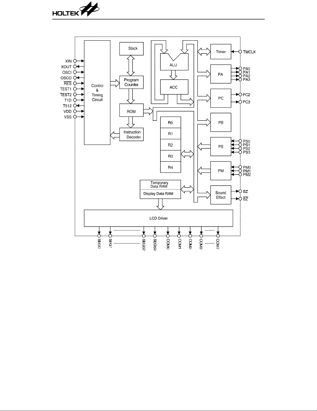
Block Diagram
HTG12N0
Notes: ACC: Accumulator R0~R4: Working registers
PB0, PB1: ROM bank switch PC0: RAM bank switch
PC1: LCD On/Off switch PA, PC2~PC3: Output ports
PS, PM0~PM2: Input ports
2 18th Mar ’99
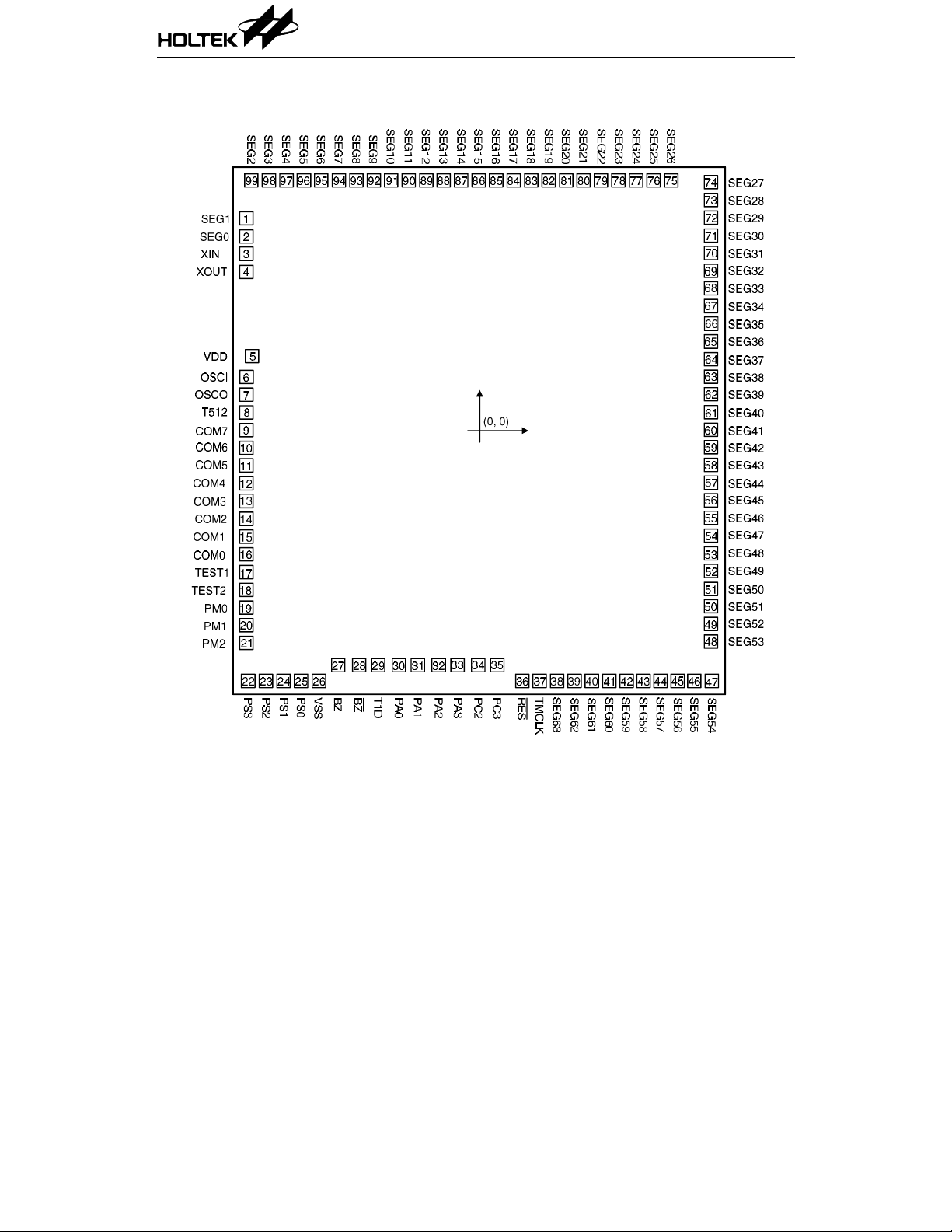
Pad Assignment
HTG12N0
Chip size: 3430 × 3730 (µm)
* The IC substrate should be connected to VSS in the PCB layout artwork.
3 18th Mar ’99
2
HTG12N0
Pad Coordinates Unit: µm
Pad No. X Y Pad No. X Y Pad No. X Y
1 –1592.40 1448.48 34 –10.08 –1598.48 67 1578.80 850.32
2 –1592.40 1324.64 35 119.04 –1598.48 68 1578.80 970.96
3 –1592.40 1207.36 36 290.48 –1706.56 69 1578.80 1091.28
4 –1592.40 1083.52 37 409.20 –1706.56 70 1578.80 1211.92
5 –1553.16 508.96 38 527.92 –1706.56 71 1578.80 1332.24
6 –1592.40 367.52 39 646.64 –1706.56 72 1578.80 1452.88
7 –1592.40 246.48 40 765.36 –1706.56 73 1578.80 1573.20
8 –1592.40 125.44 41 884.48 –1706.56 74 1578.80 1695.12
9 –1592.40 4.40 42 1001.44 –1706.56 75 1306.40 1706.56
10 –1592.40 –116.64 43 1117.60 –1706.56 76 1185.65 1706.56
11 –1592.40 –237.68 44 1233.44 –1706.56 77 1066.56 1706.56
12 –1592.40 –358.72 45 1349.60 –1706.56 78 947.12 1706.56
13 –1592.40 –479.76 46 1465.44 –1706.56 79 828.00 1706.56
14 –1592.40 –600.80 47 1584.16 –1706.56 80 708.56 1706.56
15 –1592.40 –721.84 48 1578.80 –1438.64 81 589.44 1706.56
16 –1592.40 –842.88 49 1578.80 –1318.32 82 470.00 1706.56
17 –1592.40 –963.92 50 1578.80 –1197.68 83 350.88 1706.56
18 –1592.40 –1084.96 51 1578.80 –1077.36 84 2 31.44 1706.56
19 –1592.40 –1206.00 52 1578.80 –956.72 85 112.32 1706.56
20 –1592.40 –1327.04 53 1578.80 –836.40 86 –7.12 1706.56
21 –1592.40 –1448.08 54 1578.80 –715.76 87 –126.24 1706.56
22 –1579.60 –1706.56 55 1578.80 –595.44 88 –245.68 1706.56
23 –1459.36 –1706.56 56 1578.80 –474.80 89 –364.80 1706.56
24 –1338.80 –1706.56 57 1578.80 –354.48 90 –484.24 1706.56
25 –1218.56 –1706.56 58 1578.80 –233.84 91 –603.36 1706.56
26 –1097.52 –1706.56 59 1578.80 –113.52 92 –722.80 1706.56
27 –965.12 –1598.48 60 1578.80 7.12 93 –841.92 1706.56
28 –823.20 –1598.48 61 1578.80 127.44 94 –961.36 1706.56
29 –694.08 –1598.48 62 1578.80 248.08 95 –1080.48 1706.56
30 –552.16 –1598.48 63 1578.80 368.40 96 –1199.92 1706.56
31 –423.04 –1598.48 64 1578.80 489.04 97 –1319.04 1706.56
32 –281.12 –1598.48 65 1578.80 609.36 98 –1438.48 1706.56
33 –152.00 –1598.48 66 1578.80 730.00 99 –1557.60 1706.56
4 18th Mar ’99
Pad Description
HTG12N0
Pad No. Pad Name I/O
38~99
1~2
3
4
5 VDD I — Positive power supply
6
7
8
29
17
18
9~16 COM7~COM0 O — Output for LCD panel common plate
22~25
21~19
26 VSS I — Negative power suppl y, GND
27, 28 BZ,
33~30
35~34
36
37 TMCLK I
SEG63~SEG2
SEG1~SEG0
XIN
XOUT
OSCI
OSCO
T512
T1D
TEST1
TEST2
PS3~PS0
PM2~PM0
BZ O Note 1 Sound effect outputs
PA3~PA0
PC3~PC2
RES I —
O — LCD driver outputs for LCD panel segment
I
O
I
O
O
O
I
I
I
O
Mask
Option
—
—
Pull-high or
None, Note 2
CMOS or
NMOS Open
Drain
Pull-high or
None, Note 3
Description
32768Hz crystal oscillator for time base, LCD
clock
An external resistor between OSCI and OSC0 is
needed for the internal system clock.
For test mode only
TEST1 and TEST2 are left open when the chip is
in normal operation (with an internal pull-high
resistor).
Input pins for input only
Output latch pins for output only
Input to reset an internal LSI
Reset is active on logical low level
Input for TIMER clock
TIMER can be clocked by an external clock or an
internal frequency source.
Notes:
1. The system clock provides six different sources selectable by mask option to drive the sound effect
clock. If the Holtek sound library is used, only 128K and 64K are acceptable.
2. Each bit of ports PM0~PM2, PS can be a trigger source of the HALT interrupt, selectable by mask
option.
3.14 internal clock sources can be selected by mask option to drive TMCLK. Note that TMCLK
should not be connected to a pull high resistor if an internal source is used.
5 18th Mar ’99
HTG12N0
Absolu te Maximu m R a tin g s
Supply Voltage .................................–0.3V~5.5V Storage Temperature....................–50°C~125°C
Input V oltage.....................V
Note: These are stress ratings only. Stresses exceeding the range specified under “Absolute M axi-
mum Ratings” ma y cause substantial damage to the device. Functional operation of this
device at other conditions beyond those listed in the specification is not implied and prolonged
exposure to extreme condition s may affect device reliability.
D.C. Characteristics Ta=25°C
–0.3V~VDD+0.3V Operating Temperature.....................0°C~70 °C
SS
Symbol Parameter
V
DD
I
DD
I
STB1
I
STB2
V
IL
V
IH
I
OL1
I
OH1
I
OL2
I
OH2
R
PH
Operating Voltage — — 2.4 3 3.5 V
Operating Current
(LCD ON)
Standby Current
(LCD OFF)
Standby Current
(LCD ON)
Input Low Voltage 3V — 0 — 0.2V
Input High Voltage 3V — 0.8V
PA, PC, BZ and BZ
Output Sink Current
PA, PC, BZ and BZ
Output Source Current
Segment Output Sink
Current
Segment Output Source
Current
Pull-high Resistor 3V
Test Conditions
V
DD
3V
Conditions
No load,
f
=512kHz
SYS
Min. Typ. Max. Unit
—100200
3V HALT mode — 2 5
3V HALT mode — 10 20
—VDDV
3V V
3V V
3V V
3V V
DD
=0.3V 1.5 3 — mA
OL
=2.7V –0.5 –1 — mA
OH
=0.3V 30 60 — µA
OL
=2.7V –50 –100 — µA
OH
PS, PM,
TMCLK
RES,
15 100 200 k
DD
µA
µA
µA
V
Ω
6 18th Mar ’99
HTG12N0
A.C. Characteristics Ta=25°C
Symbol Parameter
f
SYS
f
LCD
t
COM
t
CY
f
TIMER
t
RES
f
SOUND
System Clock 3V R=620kΩ~36kΩ 128 — 1000 kHz
LCD Clock 3V — — 256 — Hz
LCD Common Period — 1/8 duty — (1/f
Cycle Time 3V f
Timer I/P Frequency
(TMCLK)
Reset Pulse Width — — 5 — — ms
Sound Effect Clock — — — *64 or 128 — kHz
Test Conditions
V
DD
Conditions
=1MHz — 4 — µs
SYS
Min. Typ. Max. Unit
)×8— s
LCD
3V — 0 — 1000 kHz
*: Only these two clocking signal frequencies are supported by Holtek’s sound library.
7 18th Mar ’99
Functional Description
Program counter – PC
This counter a ddresses the program ROM and
is arranged as a 12-bit binary counter from PC0
to PC11 whose contents specify a maximum of 4096
addresses. The program counter counts with an incr ement of 1 or 2 w ith each execution of an instruction.
When executing the jump instruction (JMP,
JNZ, JC, JTMR,...), a subroutine call, initial
reset, internal inte rrupt, RTC interrupt or returning from a subroutine, the program counter
is loaded with the corresponding instruction
data as shown in the table.
Notes: P0~P11: Instruction code
@: PC11 keeps the curre nt value
S0~S11: Stack register bits
PB0 and PB1 are set to 0 at power on
reset.
Program memory – ROM
The program memory is the executable memory
and is arranged in a 4096
four banks for the program memory in HTG12N0 ,
each bank shown in the figure can be switched by
the assignment of PB0 and PB1. The address is
specified by the program counter (PC). Four sp ecial locations are reserved as shown below .
Mode
Initial
reset
Internal
interrupt
External
interrupt
Jump, call
instruction
Conditional
branch
Return from
subroutine
PC13 PC12 PC11 PC10 PC9 PC8 PC7 PC6 PC5 PC4 PC3 PC2 PC1 PC0
PB1PB00 0 0000000000
PB1PB00 0 0000000100
PB1PB00 0 0000001000
PB1 PB0 P11 P10 P9 P8 P7 P6 P5 P4 P3 P2 P1 P0
PB1 PB0 @ P10 P9 P8 P7 P6 P5 P4 P3 P2 P1 P0
PB1PB0S11S10S9S8S7S6S5S4S3S2S1S0
×8 bit format. There a re
Program memory PB0=0, PB1=0
Program memory PB0=1, PB1=0
•
Location 0
Activating the pro cessor
first instruction to be fetched from location 0.
Program Counter
HTG12N0
RES pin caus es the
Program memory
8 18th Mar ’99
•
Location 4
Contains the timer interrupt resulting from a
TIMER overflow. If the interrupts are enabled,
it causes the program to jump to this subroutine.
•
Location 8
Activating the RTC of the processor with the
interrupts enabled causes the program to
jump to this location.
•
Locations n00H to nFFH
Each page in the program memory consists of
256 bytes. This area from n00H to nFFH and
F00H to FFFH can be used as a look-up table.
Instructions such as READ R4A, READ
MR0A, READF R4A, READF MR0A can read
the table and transfer the contents of the
table to ACC and R4 or to ACC and a data
memory address specified by the register pair
R1,R0. However as R1,R0 can only store 8
bits, these instructions cannot fully specify
the full 12-bit program memory ad dress. For
this reason a jump instruction should be used
first to place the program counter in the right
page. The above instructions can then be used
to read the look up table data.
Note that the page number n must be greater
than zero as some lo cations in page 0 are reserved for specific usage as mentioned. This
area may functio n as n ormal pro gram m em ory
as required.
The program memory mapping is shown in the
diagram.
In the execution o f an instruction the program
counter is added before the execution phase, so
careful manipulation of READ MR0A and
READ R4A is required in the page margin.
Stack register
The stack register is a group of registers used to
save the contents of th e program counter (PC)
and is arranged in 13 bits
× 1 level. One bit is
used to store the carry flag. An interrupt will
force the contents o f the PC and the carry flag
onto the stack registe r. A subroutine call will
HTG12N0
Program memory PB0=0, PB1=1
Program memory PB0=1, PB1=1
also cause the PC contents to be pushed onto
the stack; however the carry flag will not be
stored. At the end o f a subroutine or a n interrupt routine wh ich is signaled by a re turn instruction, RET or RETI restore the program
counter to its previous value from the stack
register. Executing “RETI” instruction will restore the carry flag from the stack register, but
“RET” will not.
Working registers – R0, R1, R2, R3, R4
There are five working regi sters (R0, R1, R2, R3, R4)
usually used to store the frequently accessed intermediate results. Usin g the instruct ions INC Rn and
DEC Rn the working registers can increment (+1) or
decrement (–1). The JNZ Rn (n=0,1,4) instruction
makes efficient use of the wo rking registers as a
program loop counter . Also the r egister pairs R0,R1
and R2,R3 are use d as a data memory pointer when
the memory transf er instru ction is executed.
9 18th Mar ’99

HTG12N0
Data memory – RAM
The static data memory (RAM) is arranged in
256
×4 bit format and is used to store data. All of
the data memory locations are indirectly addressable through the register pair R1,R0 or
R3,R2; for example MOV A,[R3R2] or MOV
[R3R2],A.
There are two banks for data memory in
HTG12N0, each ba nk shown in the figure can
be switched by the assignment of PC0. Each
bank maps to different area of the data memory .
There are two areas in the data memory, the
temporary data area and the display data area.
Access to the temporary data area is from 00H
to 7FH of bank 0 and 00H to 7FH of bank 1,
Locations 80H to FFH (don’t care the bank
pointer) represent the display data area.
When data is written into the display data area
it is automatically read by the LCD driver
which then genera tes the corresponding LCD
driving signals.
The relationship between the data pointer RAM
locations are shown in the table.
Data memory
Data memory
Display data area (80H~FF H) don ’t care about
the PC0.
Accumulator – ACC
The accumulator is the most important data
register in the processor. It is one of the sources
of input to the ALU and the destina tion of the
results of the operations performed in the ALU.
Data to and from the I/O ports and memory also
passes through the accumulator.
Arithmetic and logic unit – ALU
This circuit performs the following arithmetic
and logical operations ...
•
Add with or without carry
•
Subtract with or without carry
•
AND, OR, Exclusive-O R
•
Rotate right, left through carry
•
BCD decimal adjust for addition
•
Increment, decrement
•
Data transfers
•
Branch decisions
The ALU not only outputs the results of data
operations, but also sets the status of the carry
flag (CF) in some instructions.
Timer/counter
The HTG12N0 contai ns a programmable 8-bit
count-up counter which can be used to count
external events or as a clock to generate an
accurate time base.
If the 8-bit timer clock is supplied by an external source from pin T MCLK, synchronization
problems may occur when reading the data
from the timer. It is therefore suggested that
the timer is stoppe d b efore retrie vin g the data .
The 8-bit counter will increment o n the rising
edge of the clock whether it is internally or
externally generated.
The timer/counter may be set and read with
software instructions and stopped by a hardware reset or a TIMER OFF instruction. To
restart the timer, load the counter with the
value XXH and then issue a TIMER ON instruction. Note that XX is the desired start
count immediate value o f the 8 bits. Once the
timer/counter is started it increments to a
maximum count o f FFH and then ove rflows to
zero (00H). It then continues to count until
stopped by a TIMER OFF instruction or a reset.
The increment from the maximum count of
FFH to zero (00H) triggers a timer flag TF and
an internal interrupt request. The interrupt
10 18th Mar ’99

HTG12N0
may be enabled or disabled by executing the EI
and DI instructions . I f the i nte rrup t is ena bled
the timer over flow will cau se a su broutine call
to location 4. The state of the timer flag can also
be tested with the conditional jump instruction
JTMR. The timer flag is cleared after the interrupt or the JTMR instruction is executed.
If an internal source is u sed, the frequency is
determined by the system clock and the parameter n as defined in the equatio n. The frequency of the internal frequency source can be
selected by mask option.
Frequency of TIMER clock
system clock
=
n
2
where n=0,1,2 ...13 selectable by mask option.
RTC
There is a real time clock (RTC) function implemented on the HTG12N0. The RTC function is used
to generate an accurate time period. The clock source
of RTC circuit comes from the 32768Hz crystal oscillator. The block diagram is shown as follows.
The RTC output can be selected by mask option.
Frequency of the RTC output =
256
n
2
, n=0~7
The RTC outp ut is used to generate an interrupt signal.
Interrupt
The HTG12N0 provid es both TI MER a nd RTC
interrupt modes. The DI and EI instructions
are used to disable an d enable the interrupts.
When the RTC is activated during enable interrupt mode and the program is not within a
CALL subroutine, this causes a subroutine call
to location 8 and reset the interrupt latch.
Likewise when th e timer flag is set in the en able interrupt mode and the program is not
within a CA LL subroutine, the TIMER inter-
rupt is activated. This cause a subroutine call to
location 4 and resets the timer flag. If both
TIMER and RTC interru pts arrive at the same
time, the RTC one will be serviced first.
When runni ng un de r a C AL L subrou tin e o r DI
the interrupt acknowle dge is on hold until th e
RET or EI instruction a invoked. The CALL
instruction should no t be used wi thi n an i nte rrupt routine as unpredictable behaviors may
occur. If within a CALL subroutine both TIMER
and RTC interrupt occur, no matter what order
they arrive in, the RTC interrupt will be serviced first after leaving the CALL subroutine.
This also applies if the two interrup t arrive at
the same time.
The interrupt are disabled by a hardware reset
or a DI instruction. They remain disabled until
the EI instruction is executed.
Initial reset
The HTG12N0 provi d es an RES pin for system
initialization. Thi s pin is equipp ed with an internal pull high resistor and in combination
with an external 0.1
an internal rese t pulse of sufficient length
µ~1µF capacitor, it provides
to
guarantee a reset to all intern al circuits. If the
reset pulse is generated externally , the
RES pin
must be held low at least 5ms.
RES is active, the inte rnal block will b e
When
initialized as sho wn below:
PC 000H
TIMER Stop
Timer flag,
Carry flag
SOUND
Reset (low)
Sound off and one sing
mode
Output port A High (or floating state)
LCD output Disabled
BZ and
BZ output High level
11 18th Mar ’99

HTG12N0
Halt
This is a special feature of the HTG12N 0 used t o
interrupt the chip’s normal operation and reduce the power consumption. When a HALT is
executed the following happens ...
•
The system clock will be stopped
•
The contents of the on-chip RAM and registers remain unchanged
•
RTC oscillator still keeps running
•
BZ and BZ keep high level output
The system can quit the HALT mode by way of
initial reset or RTC interru pt or wa ke-up from
the following entry of program counter value.
Initial reset: 00H
Wake-up: next address of the HAL T instruction
When the halt status is terminated by the RTC
interrupt, the following procedure takes place:
Case 1: If the sys tem is in an in terrup t-disabl e
state before entering the halt state:
•
The system will awake and returns to the
main program instruction following the
HALT command.
•
The RTC interrupt will be he ld until th e system receives an enable interrupt command by
which the RTC interrupt will be serviced.
Case 2: If the system is in an interru pt enable
state:
•
The RTC interrupt will awake the system and
execute the RTC interrupt subroutine.
In the HALT mode, each bit of ports PM, PS, can
be used as wake-up signal by mask option to
wake-up the system. This signal is active in
low-going transition.
Sound effects
The HTG12N0 inclu des sound effect circuitry
which offers up to 16 sounds with 3 tones, boom
and noise effects. Holtek supports a sound library including melodies, alarms, machine guns etc..
Whenever the instruction “SOUND n” or
“SOUND A” is executed, the specified sound
begins. Each time “SOUND OFF” is executed, it
immediately terminates the singing sound.
There are two singing modes, SONE mode and
SLOOP mode activated by SOUND ONE and
SOUND LOOP. In SONE mode the specified
sound plays only once. In the SLOOP mode the
specified sound keeps re-playing.
Since sounds 0~11 contain 32 notes and sounds
12~15 include 64 notes, the latter possesses
better sound than the former.
The sound effect circuit frequency can be selected by mask option.
Frequency of sound effect circuit =
system
2
clock
m
...where m=0,1,2,3,4,5.
Holtek’s sound library supports only sound
clock frequency of 128K or 64K. T o use Holtek’s
sound library the proper system clock and mask
option should be selected.
LCD display memory
As mentioned in the data memory se ction the
LCD display memory is embedded in the da ta
memory. It can be read and wri tten to in the
same way as normal data memory.
The figure illustrates the mapping between the
display memory and LCD pattern for the
HTG12N0.
There is an ON/OFF switch for display controlled by bit 1 of port PC (PC1). The corresponding
bit of the PC 1 re pres en ts “ON” o r “OF F” of the
LCD display memory.
The LCD display module may have any form as
long as the number of commons does not exceed
8 and the number of segments is not over 64.
12 18th Mar ’99

HTG12N0
LCD driver output
All of the LCD segments are random after an
initial clear. The bias voltage circuits of the
LCD display is built-in and no external resistor
is required.
The output number of the HTG12N0 LCD
driver is 64
with 1/8 duty cycle and 1/5 bias.
The LCD driving clock frequency is fixed at
256Hz. This is set by the RTC OSC (32.768kHz).
LCD driver output can be enabled or disabled
by setting PC1 without the influence of the
related memory condition.
LCD driver output is enabled by setting PC1 as
“1”, and disabled by setting PC1 as “0”.
×8 which can directly drive an LCD
LCD display memory
An example of an LC D driving waveform (1/8
duty and 1/5 bias) is shown below.
Oscillator
Only one external resi stor is required for the
HTG12N0 system clock.
The system clock is also used as th e reference
signal of the sound effect clock or internal frequency source of TIMER.
Another crystal osci llator is needed for use a s
the reference signal of LCD driving clock and
RTC interrupt clock source.
A machine cycle consists of a sequence o f four
states numbered T1 to T4. Each sta te lasts for
one oscillator period. The machine cycle is 4
if the system frequency is up to 1MHz.
RC and RTC oscillator
µs
13 18th Mar ’99

HTG12N0
Interfacing
The HTG12N0 microcontroller communicates
with the outside world through 7-bit input pins
PS and PM0~PM2 and 6- bit out put pins PA and
PC2~PC3.
Input ports – PS, PM0~PM2
All of the ports can have internal pull high
resistors determined by mask option. Every bit
of the input ports PS and PM0~PM2 can be
specified to be a trigger source for waking up
the HALT interrupt by mas k option. A high to
low transition on one of these pins will wake up
the device from a HALT status.
Input ports PS, PM0~PM2
Mask opt ions
HTG12N0 provides seven kinds of mask option
for different applications.
•
Each bit of input ports PS, PM0~PM2 with
pull-high resistor
•
Each bit of input ports PS, PM0~PM2 function as HALT wake-up trigger
•
Each bit of output port PA, PC2~PC3 with
CMOS or open drain NMOS
•
8-bit programmable TIMER with internal or
external frequency sources . There are 14 internal frequency sources which can be selected as a clocking signal.
If using internal frequency sources as clocking
signal TMCLK cannot connect with a pullhigh resistor.
•
Six kinds of sound clock frequencies:
f
/2m, m=0, 1, 2, 3, 4, 5
SYS
•
There are eight kinds of RTC interrupt frequencies. RTC interrupt frequency=256/2
n
Hz,
n=0~7.
•
Three kinds o f LCD bias current, 6µA, 15µA
and 60
µA for suitable size of LCD panel.
Outpu t port – PA, PC2~PC3
A mask option is available to select whether the
output is of a CMOS or open drain NMOS type.
After an initial clear the output port PA and
PC2~PC3 defaults to be high for CMOS or floating for NMOS.
Output port PA and PC2~PC3
14 18th Mar ’99

Application Circuits
HTG12N0
15 18th Mar ’99

Instruction Set Summary
Mnemonic Description Byte Cycle CF
Arithmetic
ADD A,[R1R0]
ADC A,[R1R0]
SUB A,[R1R0]
SBC A,[R1R0]
ADD A,XH
SUB A,XH
DAA
Logic Operation
AND A,[R1R0]
OR A,[R1R0]
XOR A,[R1R0]
AND [R1R0],A
OR [R1R0],A
XOR [R1R0],A
AND A,XH
OR A,XH
XOR A,XH
Increment and
Decrement
INC A
INC Rn
INC [R1R0 ]
INC [R3R2 ]
DEC A
DEC Rn
DEC [R1R0]
DEC [R3R2]
Data Move
MOV A,Rn
MOV Rn,A
MOV A,[R1R0]
MOV A,[R3R2]
MOV [R1R0],A
MOV [R3R2],A
MOV A,XH
MOV R1R0,XXH
MOV R3R2,XXH
MOV R4,XH
Add data memory to ACC
Add data memory with carry to ACC
Subtract data memory from AC C
Subtract data memory from ACC with borrow
Add immediate data to ACC
Subtract immediate data from ACC
Decimal adjust ACC for addition
AND data memory to ACC
OR data memory to ACC
Exclusive-OR data memory to ACC
AND ACC to data memory
OR ACC to data memory
Exclusive-OR ACC to data memory
AND immediate data to ACC
OR immediate data to ACC
Exclusive-OR immediate data to ACC
Increment ACC
Increment register, n=0~4
Increment data memory
Increment data memory
Decrement ACC
Decrement register, n=0~4
Decrement data memory
Decrement data memory
Move register to ACC, n=0~4
Move ACC to register, n=0~4
Move data memory to ACC
Move data memory to ACC
Move ACC to data memory
Move ACC to data memory
Move immediate data to ACC
Move immediate data to R1 and R0
Move immediate data to R3 and R2
Move immediate data to R4
1
1
1
1
2
2
1
1
1
1
1
1
1
2
2
2
1
1
1
1
1
1
1
1
1
1
1
1
1
1
1
2
2
2
HTG12N0
1
1
1
1
2
2
1
1
1
1
1
1
1
2
2
2
1
1
1
1
1
1
1
1
1
1
1
1
1
1
1
2
2
2
√
√
√
√
√
√
√
—
—
—
—
—
—
—
—
—
—
—
—
—
—
—
—
—
—
—
—
—
—
—
—
—
—
—
16 18th Mar ’99

HTG12N0
Mnemonic Description Byte Cycle CF
Rotate
RL A
RLC A
RR A
RRC A
Input & Output
IN A,Pi
OUT Pi,A
Branch
JMP addr
JC addr
JNC addr
JTMR addr
JAn addr
JZ A,addr
JNZ A,addr
JNZ Rn,addr
Subroutine
CALL addr
RET
RETI
Flag
CLC
STC
EI
DI
NOP
Timer
TIMER XXH
TIMER ON
TIMER OFF
MOV A,TMRL
MOV A,TMRH
MOV TMRL,A
MOV TMRH,A
Table Read
READ R4A
READ MR0A
READF R4A
READF MR0A
Rotate ACC left
Rotate ACC left through the carry
Rotate ACC right
Rotate ACC right through the carry
Input port-i to ACC, port-i=PM0~PM2,PS
Output ACC to port-i, port-i=PC2~PC3, PA
Jump unconditionally
Jump on carry=1
Jump on carry=0
Jump on timer overflow
Jump on ACC bit n=1
Jump on ACC is zero
Jump on ACC is not zero
Jump on register Rn not zero, n=0,1,4
Subroutine call
Return from subroutine or interrupt
Return from interrupt service routine
Clear carry flag
Set carry flag
Enable interrupt
Disable interrupt
No operation
Set 8 bits immediate data to TIMER
Set TIMER start counting
Set TIMER stop counting
Move low nibble of TIMER to ACC
Move high nibble of TIMER to ACC
Move ACC to low nibble of TIMER
Move ACC to high ni bble of TIMER
Read ROM code of current page to R4 and ACC
Read ROM code of current page to M(R1,R0), ACC
Read ROM code of pa g e F to R4 and ACC
Read ROM code of page F to M(R1,R0),ACC
1
1
1
1
1
1
2
2
2
2
2
2
2
2
2
1
1
1
1
1
1
1
2
1
1
1
1
1
1
1
1
1
1
1
1
1
1
1
1
2
2
2
2
2
2
2
2
2
1
1
1
1
1
1
1
2
1
1
1
1
1
1
2
2
2
2
√
√
√
√
—
—
—
—
—
—
—
—
—
—
—
—
√
0
1
—
—
—
—
—
—
—
—
—
—
—
—
—
—
17 18th Mar ’99

HTG12N0
Mnemonic Description Byte Cycle CF
Sound Control
SOUND n
SOUND A
SOUND ONE
SOUND LOOP
SOUND OFF
Activate SOUND channel n
Activate SOUND channel with ACC
Turn on SOUND one cycle
Turn on SOUND repeat cycle
Turn off SOUND
Miscellaneous
HALT Enter power down mode 2 2
2
1
1
1
1
2
—
1
—
1
—
1
—
1
—
—
18 18th Mar ’99

HTG12N0
Instruction Definitions
ADC A,[R1R0] Add data memory contents and carry to accumulator
Machine Code 0 0 0 0 1 0 0 0
Description The contents of the data memory addressed by the register pair “R1,R0”
and the carry are added to the accumulator. Carry is affected.
Operation ACC
ADD A,XH Add immediate data to accumulator
Machine Code 0 1 0 0 0 0 0 0 0 0 0 0 d d d d
Description The specified data is added to the accumulator. Carry is affected.
Operation ACC
ADD A,[R1R0] Add data memory contents to accumulator
Machine Code 0 0 0 0 1 0 0 1
Description The contents of the data memory addressed by the register pair “R1,R0” is
Operation ACC
AND A,XH Logical AND immediate data to accumulator
Machine Code 0 1 0 0 0 0 1 0 0 0 0 0 d d d d
Description Data in the accumulator is logical AND with the immediate data specified
Operation ACC
← ACC+M(R1,R0)+C
← ACC+XH
added to the accumulator. Carry is affected.
← ACC+M(R1,R0)
by a code.
← ACC “AND” XH
AND A,[R1R0] Logical AND accumulator with data memory
Machine Code 0 0 0 1 1 0 1 0
Description Data in the accumulator is logical AND with the data memory addressed
by the register pair “R1,R0”.
Operation ACC
AND [R1R0],A Logical AND data memory with accumulator
Machine Code 0 0 0 1 1 1 0 1
Description Data in the data memory addressed by the register pair “R1,R0” is logical
Operation M(R1,R0)
← ACC “AND” M(R1,R0)
AND with the accumulator
← M(R1,R0) “AND” ACC
19 18th Mar ’99

HTG12N0
CALL address Subroutine call
Machine Code 1 1 1 1 a a a a a a a a a a a a
Description The program counter bits 0~11 are saved in the stack. The program
counter is then loaded from the directly-specified address.
Operation Stack
CLC Clear carry flag
Machine Code 0 0 1 0 1 0 1 0
Description The carry flag is reset to zero.
Operation C
DAA Decimal–Adjust accumulator
Machine Code 0 0 1 1 0 1 1 0
Description The accumulator value is adjusted to the BCD (Binary Code Decimal) code,
Operation If ACC>9 or CF=1 then
DEC A Decrement accumulator
Machine Code 0 0 1 1 1 1 1 1
Description Data in the accumulator is decremented by one. Carry flag is not affected.
Operation ACC
← PC+2
PC
← address
← 0
if the contents of the accumulator is greater than 9 or C (Carry flag) is one.
ACC
← ACC+6, C ← 1
else
ACC
← ACC, C ← C
← ACC–1
DEC Rn Decrement register
Machine Code 0 0 0 1 n n n 1
Description Data in the working register “Rn” is decremented by one. Carry flag is not
affected.
Operation Rn
DEC [R1R0] Decrement data memory
← Rn–1; Rn=R0,R1,R2,R3,R4, for nnn=0,1,2,3,4
Machine Code 0 0 0 0 1 1 0 1
Description Data in the data memory specified by the register pair “R1,R0” is decre-
mented by one. Carry flag is not affected.
Operation M(R1,R0)
← M(R1,R0)–1
20 18th Mar ’99

HTG12N0
DEC [R3R2] Decrement data memory
Machine Code 0 0 0 0 1 1 1 1
Description Data in the data memory specified by register pair “R3,R2” is decremented
by one. Carry flag is not affected.
Operation M(R3,R2)
DI Disable interrupt
Machine Code 0 0 1 0 1 1 0 1
Description Internal time–out interrupt and external interrupt are disabled.
EI Enable interrupt
Machine Code 0 0 1 0 1 1 0 0
Description Internal time-out interrupt and external interrupt are enabled.
HALT Halt system clock
Machine Code 0 0 1 1 0 1 1 1 0 0 1 1 1 1 1 0
Description Turn off system clock, and enter power down mode.
Operation PC
IN A,Pi Input port to accumulator
Machine Code 0 0 1 1 0 0 1 0 PM 0 0 1 1 0 0 1 1 PS
Description The data on port “Pi” is transferred to the accumulator.
Operation ACC
← M(R3,R2)–1
← (PC)+1
← Pi; Pi=PM or PS
INC A Increment accumulator
Machine Code 0 0 1 1 0 0 0 1
Description Data in the accumulator is incremented by one. Carry flag is not affected.
Operation ACC
INC Rn Increment register
← ACC+1
Machine Code 0 0 0 1 n n n 0
Description Data in the working register “Rn” is incremented by one. Carry flag is not
affected.
Operation Rn
INC [R1R0] Increment data memory
← Rn+1; Rn=R0,R1,R2,R3,R4 for nnn=0,1,2,3,4
Machine Code 0 0 0 0 1 1 0 0
Description Data in the data memory specified by the register pair “R1,R0” is incre-
mented by one. Carry flag is not affected.
Operation M(R1,R0)
← M(R1,R0)+1
21 18th Mar ’99

HTG12N0
INC [R3R2] Increment data memory
Machine Code 0 0 0 0 1 1 1 0
Description Data memory specified by the register pair “R3,R2” is incremented by one.
Carry flag is not affected.
Operation M(R3,R2)
JAn address Jump if accumulator Bit n is set
Machine Code 1 0 0 n n a a a a a a a a a a a
Description Bits 0~10 of the program counter are replaced with the directly–specified
address, bit 11 of the program counter and PA3 of the memory bank remain, if the accumulator bit n is set to one.
Operation PC (bit 0–10)
PC
JC address Jump if carry is set
Machine Code 1 1 0 0 0 a a a a a a a a a a a
Description Bits 0~10 of the program counter are replaced with the directly–specified
address, bit 11 of the program counter and PA3 of the memory bank remain, if the C (Carry flag) is set to one.
Operation PC (bit 0~10)
PC
← M(R3,R2)+1
← address, if ACC bit n=1(n=0,1,2,3,)
← PC+2, if ACC bit n=0
← address, if C=1
← PC+2, if C=0
JMP address Direct Jump
Machine Code 1 1 1 0 a a a a a a a a a a a a
Description Bits 0~11 of the program counter are replaced with the directly–specified
address.
Operation PC
JNC address Jump if carry is not set
← address
Machine Code 1 1 0 0 1 a a a a a a a a a a a
Description Bits 0~10 of the program counter are replaced with the directly–specified
address, bit 11 of the program counter and PA3 of the memory bank remain, if the C (Carry flag) is set to zero.
Operation PC (bit 0~10)
PC
← PC+2, if C=1
JNZ A,address Jump if accumulator is not zero
← address, if C=0
Machine Code 1 0 1 1 1 a a a a a a a a a a a
Description Bits 0~10 of the program counter are replaced with the directly–specified
address, bit 11 of the program counter and PA3 of the memory bank remain, if the accumulator is not zero.
Operation PC (bit 0~10)
PC
← PC+2, if ACC=0
← address, if A CC≠ 0
22 18th Mar ’99

HTG12N0
JNZ Rn,address Jump if register is not zero
Machine Code 1 0 1 0 0 a a a a a a a a a a a R0
1 0 1 0 1 a a a a a a a a a a a R1
1 1 0 1 1 a a a a a a a a a a a R4
Description Bits 0~10 of the program counter are replaced with the directly–specified
address, bit 11 of the program counter and PA3 of the memory bank remain, if the register is not zero.
Operation PC (bit 0~10)
PC
← PC+2, if Rn=0
JTMR address Jump if time–out
Machine Code 1 1 0 1 0 a a a a a a a a a a a
Description Bits 0~10 of the program counter are replaced with the directly–specified
address, bit 11 of the program counter and PA3 of the memory bank remain, if the TF (Timer flag) is set to one.
Operation PC (bit 0~10)
PC
← PC+2, if TF=0
JZ A,address Jump if accumulator is zero
Machine Code 1 0 1 1 0 a a a a a a a a a a a
Description Bits 0~10 of the program counter are replaced with the directly–specified
address, bit 11 of the program counter and PA3 of the memory bank remain, if the accumulator is zero.
Operation PC (bit 0~10)
PC
← PC+2, if ACC≠0
← address, if Rn≠0; Rn=R0,R1,R4
← address, if TF=1
← address, if ACC=0
MOV A,Rn Move register to accumulator
Machine Code 0 0 1 0 n n n 1
Description Data in the working register “Rn” is moved to the accumulator.
Operation ACC
MOV A,TMRH Move timer to accumulator
← Rn; Rn=R0,R1,R2,R3,R4, for nnn=0,1,2,3,4
Machine Code 0 0 1 1 1 0 1 1
Description The high nibble data of the Timer counter is loaded to the accumulator.
Operation ACC
MOV A,TMRL Move timer to accumulator
← TIMER (high nibble)
Machine Code 0 0 1 1 1 0 1 0
Description The low nibble data of the Timer counter is loaded to the accumulator.
Operation ACC
← TIMER (low nibble)
23 18th Mar ’99

HTG12N0
MOV A,XH Move immediate data to accumulator
Machine Code 0 1 1 1 d d d d
Description The 4-bit data specified by code is loaded to the accumulator.
Operation ACC
MOV A,[R1R0] Move data memory to accumulator
Machine Code 0 0 0 0 0 1 0 0
Description Data in the data memory specified by the register pair “R1,R0” is moved to
Operation ACC
MOV A,[R3R2] Move data memory to accumulator
Machine Code 0 0 0 0 0 1 1 0
Description Data in the data memory specified by the register pair “R3,R2” is moved to
Operation ACC
MOV R1R0,XXH Move immediate data to R1 and R0
Machine Code 0 1 0 1 d d d d 0 0 0 0 d d d d
Description The 8-bit data specified by code are loaded to the working registers R1 and
Operation R1
← XH
the accumulator.
← M(R1,R0)
the accumulator.
← M(R3,R2)
R0, the high nibble of the data is loaded to the R1, and the low nibble of
the data is loaded to the R0.
← XH (high nibble)
R0
← XH (low nibble )
MOV R3R2,XXH Move immediate data to R3 and R2
Machine Code 0 1 1 0 d d d d 0 0 0 0 d d d d
Description The 8-bit data specified by code are loaded to the working register R3 and
R2, the high nibble of the data is loaded to the R3, and the low nibble of
the data is loaded to the R2.
Operation R3
MOV R4,XH Move imm ediate data to R4
← XH (high nibble)
R2
← XH (low nibble )
Machine Code 0 1 0 0 0 1 1 0 0 0 0 0 d d d d
Description The 4-bit data specified by code are loaded to the working register R4.
Operation R4
← XH
24 18th Mar ’99

HTG12N0
MOV Rn,A Move accumulator to register
Machine Code 0 0 1 0 n n n 0
Description Data in the accumulator is moved to the working register “Rn”.
Operation Rn
MOV TMRH,A Move accumulator to timer
Machine Code 0 0 1 1 1 1 0 1
Description The contents of accumulator is loaded to the high nibble of the timer
Operation TIMER (high nibble)
MOV TMRL,A Move accumulator to timer
Machine Code 0 0 1 1 1 1 0 0
Description The contents of accumulator is loaded to the low nibble of the timer
Operation TIMER (low nibble)
MOV [R1R0],A Move accumulator to data memory
Machine Code 0 0 0 0 0 1 0 1
Description Data in the accumulator is moved to the data memory specified by the reg-
Operation M(R1,R0)
← ACC; Rn=R0,R1,R2,R3,R4, for nnn=0,1,2,3,4
counter.
← ACC
counter.
← ACC
ister pair “R1,R0”.
← ACC
MOV [R3R2],A Move accumulator to data memory
Machine Code 0 0 0 0 0 1 1 1
Description Data in the accumulator is moved to the data memory specified by the reg-
ister pair “R3,R2”.
Operation M(R3,R2)
NOP No operation
← ACC
Machine Code 0 0 1 1 1 1 1 0
Description Do nothing, but one instruction cycle is delayed.
OR A,XH Logical OR immediate data to accumulator
Machine Code 0 1 0 0 0 1 0 0 0 0 0 0 d d d d
Description Data in the accumulator is logical OR with the immediate data specified
by code.
Operation ACC
← ACC “OR” XH
25 18th Mar ’99

HTG12N0
OR A,[R1R0] Logical OR accumulator with data memory
Machine Code 0 0 0 1 1 1 0 0
Description Data in the accumulator is logically OR with the data memory addressed
by the register pair “R1,R0”.
Operation ACC
OR [R1R0],A Logical OR data memory with accumulator
Machine Code 0 0 0 1 1 1 1 1
Description Data in the data memory addressed by the register pair “R1,R0” is logical
Operation M(R1,R0)
OUT Pi,A Output accumulator data to port-i
Machine Code 0 0 1 1 0 0 0 0 PA
Description The data in the accumulator is transferred to the port-i and latched.
Operation Pi
READ MR0A Read ROM code of current page to M(R1,R0) and ACC
Machine Code 0 1 0 0 1 1 1 0
Description The 8-bits of ROM code (current page) addressed by ACC and R4 are
Operation M(R1R0)
← ACC “OR” M(R1,R0)
OR with the accumulator.
← M(R1,R0) “ OR” ACC
0 0 1 1 0 1 0 0 PC
← ACC; Pi=PA or PC
moved to the data memory M(R1,R0) and accumulator. The high nibble of
the ROM code is loaded to M(R1,R0) and the low nibble of the ROM code is
loaded to accumulator. The address of the ROM code are specified below :
Current page
ACC
→ ROM code address bit 7~4
R4
→ ROM code address bit 3~0
ACC
← ROM code (low nibble)
→ ROM code address bit 12~8
← ROM code (hig h nibble)
READ R4A Read ROM code of current page to R4 and accumulator
Machine Code 0 1 0 0 1 1 0 0
Description The 8-bits of ROM code (current page) addressed by ACC and M(R1,R0)
are moved to the working register R4 and accumulator. The high nibble of
the ROM code is loaded to R4 and the low nibble of the ROM code is loaded
to the accumulator. The address of the ROM code are specified below:
Current page
ACC
M(R1,R0)
Operation R4
ACC
→ ROM code address bit 7~4
← ROM code (hig h nibble)
← ROM code (low nibble)
→ ROM code address bit 12~8
→ ROM code address bit 3~0
26 18th Mar ’99

HTG12N0
READF MR0A Read ROM Code of page F to M(R1,R0) and ACC
Machine Code 0 1 0 0 1 1 1 1
Description The 8-bit ROM code (page F) addressed by ACC and R4 are moved to the
data memory M(R1,R0) and accumulator. The high nibble of the ROM code
is loaded to M(R1,R0) and the low nibble of the ROM code is loaded to the
accumulator.
page F
ACC
R4
Operation M(R1,R0)
ACC
READF R4A Read ROM code of page F to R4 and accumulator
Machine Code 0 1 0 0 1 1 0 1
Description The 8-bit ROM code (page F) addressed by ACC and M(R1,R0) are moved
to the working register R4 and accumulator. The high nibble of the ROM
code is loaded to R4 and the low nibble of the ROM code is loaded to the accumulator.
page F
ACC
M(R1,R0)
Operation R4
ACC
→ ROM code address bit 12~8 are “PA3 1111”
→ ROM code address bit 7~4
→ ROM code address bit 3~0
← high nibble of ROM code (page F)
← low nibble of ROM code (page F)
→ ROM code address bit 12~8 are “PA3 1111”
→ ROM code address bit 7~4
→ ROM code address bit 3~0
← high nibble of R OM code (page F)
← low nibble of ROM code (page F)
RET Return from subroutine or interrupt
Machine Code 0 0 1 0 1 1 1 0
Description The program counter bits 0~11 are restored from the stack.
Operation PC
RETI Return from interrupt subroutine
← Stack
Machine Code 0 0 1 0 1 1 1 1
Description The program counter bits 0~11 are restored from the stack. The carry flag
before entering the interrupt service routine is restored.
Operation PC
RL A Rotate accumulator left
← Stack
C
← C (before interrupt service routine)
Machine Code 0 0 0 0 0 0 0 1
Description The contents of the accumulator are rotated left one bit. Bit 3 is rotated to
bit 0 and carry flag.
Operation An+1
← An; An: accumulator bit n (n=0,1,2)
A0
← A3
C
← A3
27 18th Mar ’99

HTG12N0
RLC A Rotate accumulator left through carry
Machine Code 0 0 0 0 0 0 1 1
Description The contents of the accumulator are rotated left one bit. Bit 3 replaces the
carry bit; the carry bit is rotated into the bit 0 position.
Operation An+1
RR A Rotate accumulator right
Machine Code 0 0 0 0 0 0 0 0
Description The contents of the accumulator are rotated right one bit. Bit 0 is rotated
Operation An
RRC A Rotate accumulator right through carry
Machine Code 0 0 0 0 0 0 1 0
Description The contents of the accumulator are rotated right one bit. Bit 0 replaces
Operation An
← An; An: Accumulator bit n (n=0,1,2)
A0
← C
C
← A3
to bit 3 and carry flag.
← An+1; An: Accumulator bit n (n=0,1,2)
A3
← A0
C
← A0
the carry bit; the carry bit is rotated into the bit 3 position.
← An+1; An: Accumulator bit n (n=0,1,2)
A3
← C
C
← A0
SBC A,[R1R0] Subtract data memory contents and carry from ACC
Machine Code 0 0 0 0 1 0 1 0
Description The contents of the data memory addressed by the register pair “R1,R0”
and the carry are subtracted from the accumulator. Carry is affected.
Operation ACC
SOUND A Active SOUND channel with accumulator
← ACC+M(R1,R0)+CF
Machine Code 0 1 0 0 1 0 1 1
Description The activated sound begins playing in accordance with the contents of the
accumulator when the specified sound channel is matched.
SOUND LOOP Turn on sound repeat mode
Machine Code 0 1 0 0 1 0 0 1
Description The activated sound plays repeatedly.
SOUND OFF Turn off sound
Machine Code 0 1 0 0 1 0 1 0
Description The singing sound will terminate immediately.
28 18th Mar ’99

HTG12N0
SOUND ONE Turn on sound one mode
Machine Code 0 1 0 0 1 0 0 0
Description The activated sound plays only one tim e.
SOUND n Active SOUND Channel n
Machine Code 0 0 0 0 n n n n 0 1 0 0 0 1 0 1
Description The specified sound begins playing and overwriting the previous singing
sound. (nnn=0~15)
STC Set carry flag
Machine Code 0 0 1 0 1 0 1 1
Description The carry flag is set to one.
Operation C
SUB A,XH Subtract immediate data from accumulator
Machine Code 0 1 0 0 0 0 0 1 0 0 0 0 d d d d
Description The specified data is subtracted from the accumulator. Carry is affected.
Operation ACC
SUB A,[R1R0] Subtract data memory contents from accumulator
Machine Code 0 0 0 0 1 0 1 1
Description The contents of the data memory addressed by the register pair “R1,R0” is
Operation ACC
← 1
← ACC+XH+1
subtracted from the accumulator. Carry is affected.
← ACC+M(R1,R0)+1
TIMER OFF Set timer to stop counting
Machine Code 0 0 1 1 1 0 0 1
Description The timer stops counting when the “TIMER OFF” instruction is executed.
TIMER ON Set timer start counting
Machine Code 0 0 1 1 1 0 0 0
Description The timer starts counting when the “TIMER ON” instruction is executed.
TIMER XXH Set immediate data to timer counter
Machine Code 0 1 0 0 0 1 1 1 d d d d d d d d
Description The 8-bit data specified by code is loaded to the Timer counter .
Operation TIMER
← XXH
29 18th Mar ’99

HTG12N0
XOR A,XH Logical XOR immediate data to accumulator
Machine Code 0 1 0 0 0 0 1 1 0 0 0 0 d d d d
Description Data in the accumulator is Exclusive-OR with the immediate data speci-
fied by code.
Operation ACC
XOR A,[R1R0] Logical XOR accumulator with data memory
Machine Code 0 0 0 1 1 0 1 1
Description Data in the accumulator is Exclusive-OR with the data memory addressed
Operation ACC
XOR [R1R0],A Logical XOR data memory with accumulator
Machine Code 0 0 0 1 1 1 1 0
Description Data in the data memory addressed by the register pair “R1,R0” is logi-
Operation M(R1,R0)
← ACC “XOR” XH
by the register pair “R1,R0”.
← ACC “XOR” M(R1,R0)
cally Exclusive-OR with the accumulator.
← M(R1,R0) “XO R” ACC
30 18th Mar ’99
 Loading...