


HT9580
Preliminary
Character Pager Controller
Features
Operating voltage: 2.4V~3.5V
·
Temperature range: -30°Cto+85°C
·
low power, high performance M6502 core
·
low power crystal oscillator control
·
-
512/1200/2400 bps data rate operation
²CCIR Radio Paging Code No.1² (POCSAG)
·
compatible
76.8kHz crystal for all available data rates
·
High/low system clock switching capability
·
44 Kbytes program ROM
·
848 bytes global data RAM
·
Internal 2 Mbits Character ROM
·
256 Kbits internal SRAM
·
External option up to 2 Mbits Character
·
ROM or 2 Mbits SRAM
SED15X(KSX), MC141X and HD66410
·
series LCD driver compatible interface
option
46 bytes message buffer
·
One 16-bit timer and one 8-bit timer
·
General Description
The HT9580 is a high performance pager controller which can be used for Chinese Pager
system applications. The HT9580 4-in-1 Character Pager Controller combines a POCSAG decoder with a M6502 microprocessor core, 2
Mbits Character ROM and 256 Kbits SRAM to
provide both high decoder performance and excellent system flexibility. The decoder utilizes a
2-bit random error correction algorithm and
Internal 2Hz or 1Hz RTC or Real Time
·
Clock option
Single buzzer generator output (BZ) with
·
duty cycle control
low current HALT mode operation
·
16-bit watchdog timer
·
Built-in data filter (16-times over-sampling )
·
and bit clock recovery
Advanced synchronization algorithm
·
2-bit random and (optional) 4-bit burst er
·
ror correction for address and message
Up to 6 user addresses and 6 user frames,
·
independently programmable
3 RF power-on timing control pins
·
and Received data inversion (optional)
Built in SPI circuit
·
Out-of-range condition indicator
·
One internal 8-bit D/A converter
·
Battery fail and battery low detection
·
80-pin LQFP package
·
therefore provides excellent decoder sensitivity. The controller contains a full function
pager decoder at a 512, 1200, 2400 bps data
rates. Using an M6502 core takes advantage of
a flexible external control interface, LCD driver
chips and abundant programming resources
from worldwide providers. The internal SPI
would communicate with SPI of FLEX
speed pager decoder.
TM
high
-
FLEXTMis a trademark of Motorola Inc.
1 April 28, 2000
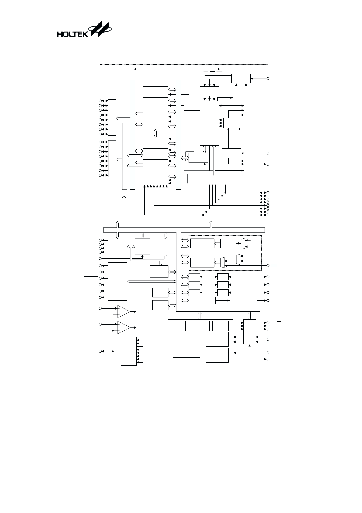
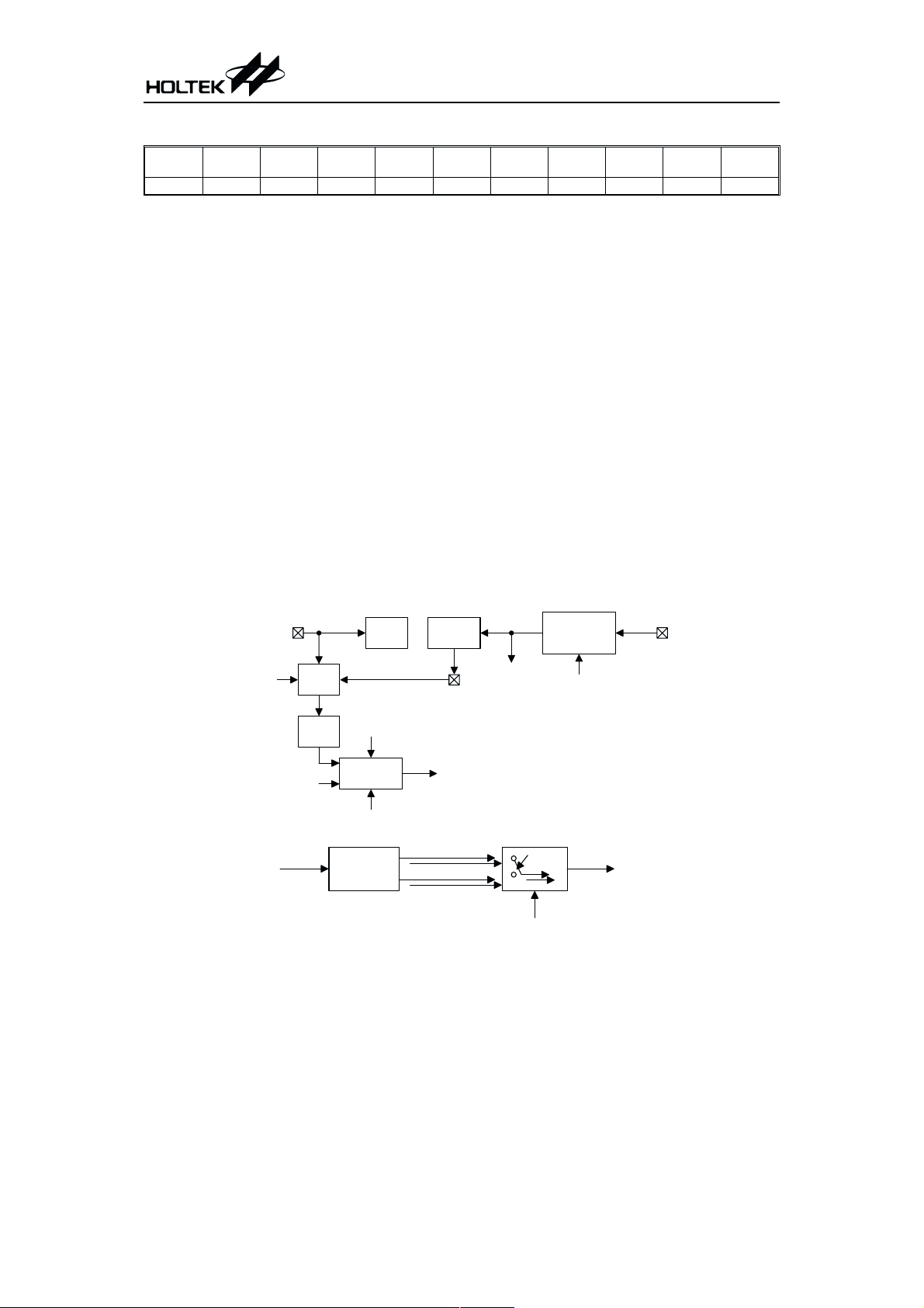
Block Diagram
Preliminary
HT9580
A10
A11
A12
A13
A14
A15
RA14
RA15
RA16
RA17
P_MO DE
LC D _E
LC D _R W
LCD_CS0
LCD_CS1
LCD_CL
LCD_A0
RSSI
R egister S ection C ontrol Section
Index
R egister
Y
Program
ROM
Index
R egister
X
S tack P o int
R egister (s)
ALU
A ccum ulator
A
PCL
PCH
Input Data
Latch
(D L )
Data Bus
B u ffe r
C haracter
ROM
WDT
RTC
SRAM
Special B us
Processor
Status
R egister P
PAC
PBC
PCC
Tone G enerator
A0
A1
A2
A3
ABL
A4
A5
A6
A7
A8
A9
ABH
Address
D ecoder
In te rfa c e
M 6502 C o re
LC D
Driver
In te rn a l A D L
In te rn a l A D L
Legend
=8 Bit Line
=1 Bit Line
RES
Interrupt
Logic
Instruction
D ecoder
TM R 0 (8 bit)
TM R 1 (16 bit)
IR Q
Interrupt
Logic
NMI
P re -scale r
PA
PB
PC
Logic
NMI IR Q
VP
Tim ing
C ontrol
Clock
G enerator/
O scillator
MUX
D u ty C yc le C o n tro l
RDY
SYNC
ML
P H I2 (IN )
PHI1 (OU T)
PHI2 (O UT)
SO
R/W
BE
MUX
X1
S ystem C lock
MUX
X1
S ystem C lock
RESET
OSC1
OSC2
D0
D1
D2
D3
D4
D5
D6
D7
TM R 1
PA0~PA5
PB0~PB7
PC0~PC1
BZ
BAF
DA_OUT
8-bit
D/A
DA7
DA6
DA5
DA4
DA3
DA2
DA1
DA0
Digital
F ilte r
BCH Code
D ecoder
C ontroller
Status
D ata Phase
R eco very
U ser Address
C onfiguration
POCSAG Decoder
R F P ow er
C ontroller
and
Memory
D ecoder
Data
O utput
C ontrol
SPI
Circuit
SPI Control
BS1/SS
BS2/SCK
BS3/M OSI
D I/M IS O
BAL/SRDY
X1
X2
2 April 28, 2000
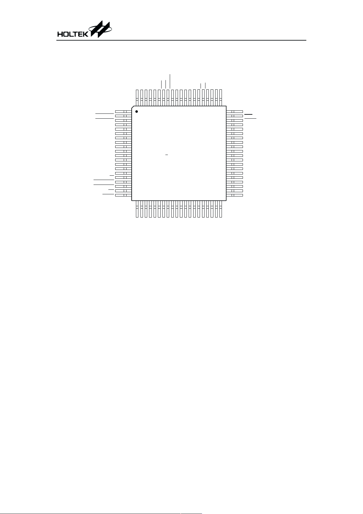
Pin Assignment
X1
Preliminary
RESET
OSC2
OSC1
TSC
X2
VSS
TS1
PA2
PA1
PA0
HT9580
BS3/M OSI
BS2/SCK
D I/M IS O
BS1/SS
PA5
PA4
PA3
TS
RSSI
VDD
LC D _C S 1
LC D _C S 0
LC D _C L
LC D _A 0
LC D _R W
LC D _E
D7
D6
D5
D4
D3
D2
D1
D0
R/W
SRAM _CE
MASK_CE
OE
PSEN
1
H T9580
80 LQ FP
20
21 40
RA17
RA16
RA15
RA14
P_M ODE
A15
VSS
VDD
A14
A13
A12
A11
A10
A9
A8
A7
A6
A5
A4
6180
60
41
A3
DA_OUT
BAF
SRD Y/BAL
VSS
VDD
BZ
PC1
PC0
PB7
PB6
PB5
PB4
PB3
PB2
PB1
PB0
TM R1
A0
A1
A2
3 April 28, 2000
Preliminary
HT9580
Pin Description
Pin No. Pin Name I/O Description
1, 25, 56 VDD
2 LCD_CS1
3 LCD_CS0
4 LCD_CL O LCD driver clock output
5 LCD_A0 O LCD driver data/command select control
6 LCD_RW O LCD Driver Read/Write signal output
7 LCD_E O LCD driver enable clock control
15~8 D0~D7 I/O 8-bit, tristate, bidirectional I/O data bus.
16 R/W
17 SRAM_CE
18 MASK_CE
19 OE
20 PSEN O
21~24 RA17~RA14 O Extended address bus pins
26 P_MODE I
27, 57, 78 VSS
43~28 A0~A15 O
44 TMR1 I Schmitt trigger input for timer1 counter with pull-high resisor.
45~52 PB0~PB7 I/O
53~54 PC0~PC1 I/O
55 BZ O Buzzer non-inverting BZ output
Positive power supply
¾
O LCD driver chip select control (for slave LCD driver)
O LCD driver chip select control (for master LCD driver)
O Read/Write signal output
SRAM chip Enable. This signal is generated from the HT9580 to
O
provide read or write timing for external SRAM devices. (See Ap
plication Circuit)
Mask ROM Chip Enable. This signal is generated from the
O
HT9580 to provide read timing for external Mask ROM devices.
(See Application Circuit)
Mask ROM or SRAM Output Enable. This signal is generated
O
from the HT9580 to provide read timing for external Mask ROM
and SRAM devices. (See Application Circuit)
Program Store Enable. This pin is used to connect the OE
pins of the external 44 Kbytes program ROM when the
²MODE_P² internal pad is connected to VSS. (See note)
Internal or external program ROM selection without pull-high resistor. If the pin connects to VDD, the internal program ROM will
be fetched (normal type), otherwise the external program ROM
will be fetched when the pin connects to VSS (Romless).
Negative power supply
¾
Address bus pins. This is used for memory and I/O exchanges on
the data bus.
General Input/Output Port B. The input cell structures can be se
lected as CMOS or CMOS with pull-high resistors.
General Input/Output Port C. The input cell structures can be se
lected as CMOS or CMOS with pull-high resistors.
and CE
-
-
-
4 April 28, 2000
Preliminary
Pin No. Pin Name I/O Description
BAL I Battery voltage detector input with pull-high resistor.
SPI slave ready ¾ This slave ready pin is a Schmitt trigger input
58
59 BAF
60 DA_OUT O D/A converter output. This pin is an 8-bit D/A analog output
61 RSSI I
62
63
64
65
66 TS
72~67 PA0~PA5 I/O
73 RESET I Schmitt trigger reset input, active low.
74 TSC
75 TS1
77
76
80
79
SRDY
DI I
MISO I
BS3 O PLL power control enable, CMOS output
MOSI O
BS2 O RF quick charge control enable, CMOS output
SCK I/O
BS1 O Pager receiver power control enable output, CMOS output
SS
OSC1
OSC2
X1
X2
with pull-high resistor. When the slave initiates the SPI transfer,
I
a high to low transition activates an interrupt. When the master
initiates the SPI transfer, a high to low transition trigger the
master to start the transfer.
I Battery fail indication input, active low.
RSSI output from IF circuit. This pin should be pulled high or low
externally when this pin is not used.
POCSAG code input serial data. CMOS input with pull-high re
sistor.
SPI master-in-slave-out ¾ this is the data input with pull-high
resistor for SPI communications.
SPI master-out-slave-in ¾ this is the data output for SPI commu
nications.
SPI serial clock ¾ the SCK signal is used to synchronize the data
transfer. If HT9580 is in the master mode, the SCK is output
clock. Otherwise, SCK is input clock if HT9580 is in the slave
mode.
SPI slave select ¾ this signal is used to enable the SPI slave for
O
transfer.
I Decoder test mode input pin, active low with pull-high resistor.
General Input/Output Port A. These ports can be programmed to
have a wake-up capability for applications in keyboard operations
or as normal I/O. Also the input cell structures are all Schmitt
trigger types and can be selected between CMOS or CMOS with
pull-high resistors.
mC test mode input pin, active low with internal pull-high resis
I
tor. The test circuit will be activated when this pin pulls low.
Decoder test mode input pin, active low with pull-high resistor.
I
The internal test mode will be activated when this pin pulls low.
IOOSC1 and OSC2 are connected to an RC network to form a main
clock oscillator
IOX1 and X2 are connected to a crystal to form an internal low power
clock oscillator (32.768kHz, 76.8kHz, or 153.6kHz)
HT9580
-
-
-
5 April 28, 2000
Absolute Maximum Ratings
Preliminary
HT9580
Supply Voltage ..............................-0.3V to 3.6V
Input Voltage .................V
Current Drain Per Pin Excluding V
-0.5V to VDD+0.5V
SS
and VSS............................................................................10mA
DD
Storage Temperature.................-55°Cto150°C
Operating Temperature ..............-30°Cto85°C
Note: These are stress ratings only. Stresses exceeding the range specified under ²Absolute Maxi
mum Ratings² may cause substantial damage tothe device.Functional operation of this de
vice at other conditions beyond those listed in the specification is not implied and prolonged
exposure to extreme conditions may affect device reliability.
D.C. Characteristics
Symbol Parameter
V
DD
Operating Voltage
Test Conditions
V
DD
¾
Conditions
3V application 2.4 3.0 3.5 V
Min. Typ. Max. Unit
Ta=25°C
No load,
I
I
V
V
V
V
V
V
V
V
I
I
I
I
I
I
R
R
DD
STP
IL
IH
IL1
IH1
IL2
IH2
OL
OH
OL
OH
OL1
OH1
OL2
OH2
OSC
PH
Operating Current 3V
HALT Mode Current 3V
Input low Voltage for
I/O Port
Input High Voltage for
I/O Port
3V
3V
Input low Voltage 3V
Input High Voltage 3V
Input low Voltage (BAF)3V
Input High Voltage (BAF)3V
Output low Voltage 3V
Output High Voltage 3V
I/O Port Sink Current 3V
I/O Port Source Current 3V
BZ, PC0~PC1 Sink Current 3V
BZ, PC0~PC1 Source Current 3V
BS1, BS2, BS3 Sink Current 3V
BS1, BS2, BS3 Source Current 3V
RC Oscillator Resistor 3V
I/O Port Pull-high
Resistance
3V
OSC1=1MHz
f
=76.8kHz
X1
No load, mC clock stop,
=76.8kHz
f
X1
¾
¾
¾
¾ 0.7´V
¾
¾
¾¾¾
¾
V
=0.3V
OL
V
=2.7V
OH
V
=0.3V
OL
V
=2.7V
OH
V
=0.3V
OL
V
=2.7V
OH
f
=1MHz
OSC
¾
0.7´V
1.0
2.3
2.0 3.6
-1.2 -2.2 ¾
-1.5 -2.5 ¾
350
-1.0 ¾¾
100 250
300
¾
¾¾
0
DD
0
DD
0
0.3´V
¾
¾
¾ 0.3´V
¾
¾
¾
¾¾
2 4.5
¾¾mA
¾
51
¾mA
100
DD
mA
V
3V
V
DD
3V
0.9 V
3V
0.4 V
V
¾
mA
mA
¾
mA
mA
mA
¾ kW
¾ kW
-
-
6 April 28, 2000
Preliminary
HT9580
A.C. Characteristics
Symbol Parameter
f
OSC1
D
OSC1
f
X1
t
RESET
Main Clock (RC OSC) 3V
Main Clock Duty Cycle 3V
Pager Clock Input (Crystal OSC) 3V
RESET Input Pulse Width
Functional Description
Memory map
0000H
003BH
0040H
006D H
0080H
01C FH
01D 0H
01FFH
0200H
03FFH
1000H
2FFFH
3000H
4FFFH
5000H
I/O and Data Space
G lobal D ata M em ory
G lobal D ata M em ory
60 Bytes
M essage B uffer
46 Bytes
336 Bytes
S tacks
48 Bytes
512 Bytes
Internal/External
C haracter R O M
8 Kbytes
Internal/External
SRAM
8 Kbytes
Test Conditions
Conditions
V
DD
¾
¾
¾
¾¾
1000H
C haracter R O M
2FFFH
Bank0~B ank31 (2 M bits)
1000H
C haracter R O M
2FFFH
Bank0~B ank31 (2 M bits)
Ta=25°C
Min. Typ. Max. Unit
76.8 1000 2000 kHz
40 50 60 %
32.768 76.8 153.6 kHz
Internal
Space
(Bank 0)
8 Kbytes
External
Space
(Bank 0)
8 Kbytes
1
¾¾
ms
BFFFH
C 000H
FFFAH
FFFBH
FFFCH
FFFDH
FFFEH
FFFFH
Program R O M S pace
28 KB ytes
Program R O M S pace
16378 Bytes
NMI-L
NMI-H
RESET-L
RESET-H
IR Q - L
IR Q - H
3000H
4FFFH
3000H
4FFFH
Internal
SRAM
Space
(Bank 0)
8 Kbytes
Bank0~B ank3 (32 K B ytes)
External
SRAM
Space
(Bank 0)
8 Kbytes
Bank0~B ank31 (256 K B ytes)
7 April 28, 2000
Preliminary
HT9580
HT9580 memory mapping table (I/O and data space)
Address
0000H Config. HALT CLK_SEL OSC_MOD LPM RTC BZ_CLK MDUT MGEN 0001 0000
0001H WDT-TMR X X TMR0_PR1 TMR0_PR0 WDTEN WS2 WS1 WS0 0000 0111
0002H CLR WDT X X X X X X X X uuuu uuuu
0003H BZ-L BZL7 BZL6 BZL5 BZL4 BZL3 BZL2 BZL1 BZL0 0000 0000
0004H BZ-H BZH7 BZH6 BZH5 BZH4 BZH3 BZH2 BZH1 BZH0 0000 0000
0005H INT ctrl 0 0 0 RTCEN ORMSK RTCMSK TM1IMSK TM0IMSK 0000 1111
0006H INT flag 0 RTC_FG DR_FG BF_FG WDTOVFG OR_FG TM1OVFG TM0OVFG 0000 0000
0007H TMRC TMR1MOD X TMR1CLK TMR0CLK TMR1EDG TMR0EDG TMR1EN TMR0EN 0000 0000
0008H TMR1L TM1D7 TM1D6 TM1D5 TM1D4 TM1D3 TM1D2 TM1D1 TM1D0 uuuu uuuu
0009H TMR1H TM1D15 TM1D14 TM1D13 TM1D12 TM1D11 TM1D10 TM1D9 TM1D8 uuuu uuuu
000AH TMR0 TM0D7 TM0D6 TM0D5 TM0D4 TM0D3 TM0D2 TM0D1 TM0D0 uuuu uuuu
000BH PA data X X PA5 PA4 PA3 PA2 PA1 PA0 uu11 1111
000CH PB data PB7 PB6 PB5 PB4 PB3 PB2 PB1 PB0 1111 1111
000DH PC data X X X X X X PC1 PC0 uuuu uu11
000EH PAC X X PAC5 PAC4 PAC3 PAC2 PAC1 PAC0 uu11 1111
000FH PBC PBC7 PBC6 PBC5 PBC4 PBC3 PBC3 PBC1 PBC0 1111 1111
0010H PCC X X X X X X PCC1 PCC0 uuuu uu11
0011H PA WUE X X PAWUE5 PAWUE4 PAWUE3 PAWUE2 PAWUE1 PAWUE0 uu00 0000
0012H PA IM X X PAIM5 PAIM4 PAIM3 PAIM2 PAIM1 PAIM0 uu11 1111
0013H PB IM PBIM7 PBIM6 PBIM5 PBIM4 PBIM3 PBIM2 PBIM1 PBIM0 1111 1111
0014H PC IM X X X X X X PCIM1 PCIM0 uuuu uu11
0015H MROM-BP BP_MODM1 BP_MODM0 M_BP5 M_BP4 M_BP3 M_BP2 M_BP1 M_BP0 0000 0000
0016H SRAM-BP BP_MODS1 BP_MODS0 S_BP5 S_BP4 S_BP3 S_BP2 S_BP1 S_BP0 0000 0000
0017H LCD_CTRL LCD-CHIP1 LCD-CHIP0 LCD-CLK CLK-MOD LCD-CS1 LCD-CS0 LCD-A0 LCD-WRB 0000 1101
0018H LCD_CMD LCD_D7 LCD_D6 LCD_D5 LCD_D4 LCD_D3 LCD_D2 LCD_D1 LCD_D0 uuuu uuuu
0019H
001AH~
002EH
002FH D/A-L DA7 DA6 DA5 DA4 DA3 DA2 DA1 DA0 0000 0000
0030H D/A-H X X X X X D/A_PD RSSI BAT uuuu u1uu
0031H
0032H SPI-CONFIG S/M LEN1 LEN0 REQST SPIFG CLK_EDG SPI_EN START 0111 1000
0033H SPI-SPEED SP7 SP6 SP5 SP4 SP3 SP2 SP1 SP0 0000 0000
0034H SPI-OUT3 D7 D6 D5 D4 D3 D2 D1 D0 0000 0000
0035H SPI-OUT2 D7 D6 D5 D4 D3 D2 D1 D0 0000 0000
0036H SPI-OUT1 D7 D6 D5 D4 D3 D2 D1 D0 0000 0000
0037H SPI-OUT0 D7 D6 D5 D4 D3 D2 D1 D0 0000 0000
0038H SPI-IN3 D7 D6 D5 D4 D3 D2 D1 D0 0000 0000
0039H SPI-IN2 D7 D6 D5 D4 D3 D2 D1 D0 0000 0000
003AH SPI-IN1 D7 D6 D5 D4 D3 D2 D1 D0 0000 0000
003BH SPI-IN0 D7 D6 D5 D4 D3 D2 D1 D0 0000 0000
Register
Name
Decoder
Control/
flag
Decoder
Configuration
Memory
Buffer
Status
Bit 7 Bit 6 Bit 5 Bit 4 Bit 3 Bit 2 Bit 1 Bit 0
XBL
MSG_END X count_5 count_4 count_3 count_2 count_1 count_0 0uuu uuuu
OR X STB X RES ON uu0u uu01
State on
uuuu uuuu
POR
8 April 28, 2000
Preliminary
HT9580
HT9580 memory attribute table (I/O and data space)
Address
0000H Config. R/W R/W R/W R/W R/W R/W R/W R/W 0001 0000
0001H WDT-TMR X X R/W R/W R/W R/W R/W R/W 0000 0111
0002H CLR WDT W W W W W W W W uuuu uuuu
0003H BZ-L R/W R/W R/W R/W R/W R/W R/W R/W 0000 0000
0004H BZ-H R/W R/W R/W R/W R/W R/W R/W R/W 0000 0000
0005H INT ctrl 0 0 0 R/W R/W R/W R/W R/W 0000 1111
0006H INT flag 0 R/W R/W R R/W R/W R/W R/W 0000 0000
0007H TMRC R/W X R/W R/W R/W R/W R/W R/W 0000 0000
0008H TMR1L R/W R/W R/W R/W R/W R/W R/W R/W uuuu uuuu
0009H TMR1H R/W R/W R/W R/W R/W R/W R/W R/W uuuu uuuu
000AH TMR0 R/W R/W R/W R/W R/W R/W R/W R/W uuuu uuuu
000BH PA data X X R/W R/W R/W R/W R/W R/W uuuu uuuu
000CH PB data R/W R/W R/W R/W R/W R/W R/W R/W uuuu uuuu
000DH PC data X X X X X X R/W R/W uuuu uuuu
000EH PAC X X R/W R/W R/W R/W R/W R/W uu11 1111
000FH PBC R/W R/W R/W R/W R/W R/W R/W R/W 1111 1111
0010H PCC X X X X X X R/W R/W uuuu uu11
0011H PA WUE X X R/W R/W R/W R/W R/W R/W uu00 0000
0012H PA IM X X R/W R/W R/W R/W R/W R/W uu00 0000
0013H PB IM R/W R/W R/W R/W R/W R/W R/W R/W 0000 0000
0014H PC IM X X X X X X R/W R/W uuuu uu00
0015H MROM-BP R/W R/W R/W R/W R/W R/W R/W R/W 0000 0000
0016H SRAM-BP R/W R/W R/W R/W R/W R/W R/W R/W 0000 0000
0017H LCD_CTRL R/W R/W R/W R/W R/W R/W R/W R/W 0000 1101
0018H LCD_CMD R/W R/W R/W R/W R/W R/W R/W R/W uuuu uuuu
0019H
001AH~
002EH
002FH D/A-L R/W R/W R/W R/W R/W R/W R/W R/W 0000 0000
0030H D/A-H X X X X X R/W R R uuuu u1uu
0031H
0032H SPI-CONFIG R/W R/W R/W R R R/W R/W R/W 0111 1000
0033H SPI-SPEED R/W R/W R/W R/W R/W R/W R/W R/W 0000 0000
0034H SPI-OUT3 R/W R/W R/W R/W R/W R/W R/W R/W 0000 0000
0035H SPI-OUT2 R/W R/W R/W R/W R/W R/W R/W R/W 0000 0000
0036H SPI-OUT1 R/W R/W R/W R/W R/W R/W R/W R/W 0000 0000
0037H SPI-OUT0 R/W R/W R/W R/W R/W R/W R/W R/W 0000 0000
0038H SPI-IN3 R R R R R R R R 0000 0000
0039H SPI-IN2 R R R R R R R R 0000 0000
003AH SPI-IN1 R R R R R R R R 0000 0000
003BH SPI-IN0 R R R R R R R R 0000 0000
Note:
Register
Name
Decoder
Control/
flag
Decoder
Configuration
Memory
Buffer
Status
²R² Read Only
²W² Write Only
²R/W² Read or Write
²X² N/A
Bit 7 Bit 6 Bit 5 Bit 4 Bit 3 Bit 2 Bit 1 Bit 0
X R/W R X R X R/W R/W uu0u uu01
R/W R/W R/W R/W R/W R/W R/W R/W uuuu uuuu
R X R R R R R R 0uuu uuuu
State on
POR
9 April 28, 2000y
Preliminary
HT9580
Configuration register
Address
0000H Config. HALT CLK_SEL OSC_MOD LPM RTC BZ_CLK MDUT MGEN 0001 0000
Register
Name
Bit 7 Bit 6 Bit 5 Bit 4 Bit 3 Bit 2 Bit 1 Bit 0
State on
POR
Oscillator configuration
There are two clock source input pins on the
chip, the main clock and the pager decoder in
put clock. The main clock is generated by an RC
network. The system clock may be the OSC in
put or the X1-clock depending on bit
²CLK_SEL². The pager decoder input clock co
mes from two external pins, X1 and X2. The fre
quency of the sub-clock will be double that of
the X1, X2 input clock. The OSC1 main clock
will be generated from an RC network that
needs an external resistor (see Application Cir
cuit). The system clock may be X1-clock, DF or
RC clock. If no higher frequency (RC) is needed,
the external resistor between OSC1 and OSC2
can be removed. The system clock can be
switched by bit ²CLK_SEL².If²CLK_SEL²=0
(POR State), the system clock will be X1-clock.
In other cases, with ²CLK_SEL²=1, the OSC in
put clock will be the system clock. The clock
switching function will assist software programmers to change the mC system clock within an adequate time if necessary. The
OSC1
OSC_MOD
0: R C
1 : D F
OSC
C ontrol
OSC
Input
HALT
Main
Clock
Frequency
Sub-clock
²OSC_MOD² bit selects the OSC input clock to
be either RC or DF. If ²OSC_MOD² is set to
²low² then the RC configuration is selected, oth
erwise the DF application is selected. The pro
grammer should note that the condition of
²CLK_SEL², ²HALT² and ²OSC_MOD² assures
that the system clock is working properly. It is
recommended that the OSC clock source is ei
ther DF or RC. If DF and RC are necessary, it is
required to switch the system clock to X1-clock
before switching between DF and RC. Then
switch the system clock back to the OSC input
by using bit CLK_SEL if the switching action of
DF and RC is complete. Before enter HALT
mode, the system clock must select X1-clock.
The HT9580 will generate two RTC frequen
cies, 1Hz and 2Hz respectively, determined by
bit RTC. If the bit is logic low, the 1Hz RTC fre
-
quency will be selected, otherwise the 2Hz RTC
frequency will be selected. The RTC counter is
enabled/disabled by bit RTCEN and can be
masked or not masked as determined by the bit
RTCMSK of the interrupt control register
SST
D oubler
DF
X1-clock
10-bit R ipple
C ounter
SST Control
X1
-
-
-
-
-
X1-clock
X1-clock
C lock S e lect
CLK_SEL
C ounter
S ystem C lock
0: X 1-clock
1: O SC Input
1H z & Tim e O ut
2H z & Tim e O ut
RTC block diagram
10 April 28, 2000
RTC Tim e Out
RTC
Preliminary
(0005H). If the RTC counter is enabled, the
RTC counter will start to count. The RTC coun
ter source clock is the X1-clock, so the X1 clock
setting via by SPF12, SPF13 and SPF14 should
be correct.
In order to guarantee that the system clock has
started and stabilized, the SST (System
Start-up Timer) provides an extra delay of 1024
system clock pulse when the system is powered
up.
10
Select 2Hz as the
RTC
RTC
The low power oscillator of the pager decoder
input clock should be crystal type. The decoder
subsystem low power oscillator, on the other
hand, is of a crystal type which is designed with
a power on start-up function to reduce the sta
bilization time of the oscillator. This start-up
function is enabled by bit ²LPM² which is ini
tially set high at power on reset, and should be
cleared to low so as to enable the low-power os
cillator function. The oscillator configuration is
running in the low power mode.
The system clock oscillator can be enabled/dis
abled by the register bit, ²HALT². The system
clock circuit is powered down, when the bit is
set to high. On the other hand, the system clock
Select 1Hz as the
RTC
V
DD
-
100k
W
50k
W
50k
W
100k
W
VSS
L o w p o w e r o s c illa to r fu n c t io n
LPM
(Low power m ode control)
X2
H T 9580
X1
low power oscillator
circuit is powered up, when the bit is low. When
this bit is set high, the CPU is also stopped.
-
When this bit is cleared low, the CPU core re
turns to its normal operation. After this is set
HIGH by the software, it may also be cleared
low when reset, interrupt (IRQ
timeout, and port wake-up conditions are met.
or NMI), RTC
01
-
HALT
System clock
enable
System clock
powered down
The WDT is a 16-bit counter and sourced by the
HT9580
-
WDT-TMR (Watchdog timer) register
Address
0001H WDT-TMR X X TMR0_PR1 TMR0_PR0 WDTEN WS2 WS1 WS0 0000 0011
0002H CLR WDT XXXXXXXXuuuu uuuu
sub-clock divided by 8. The counter is seg
mented as a 9-bit prescaler and a 7-bit user pro
grammable counter. The input clock is first
divided by 512 (9-stage) to get the nominal
time-out period. The output of the 9-bit
pre-scaler can then be divided by a 7-bit pro
grammable counter to generate the longer
watchdog time-out depending on the user¢sre
quirements. The 7-bit programmable counter is
controlled by 3 register bits, WS0~2. The
watchdog timer is enabled/disabled by a control
bit WDTEN. To prevent the overflow of this
Register
Name
Bit 7 Bit 6 Bit 5 Bit 4 Bit 3 Bit 2 Bit 1 Bit 0
-
be executed before the timer overflows. The
clear-WDT operation is to write any number to
the register, CLRWDT (0002H). When the
watchdog timer overflows (checked by bit 3 of
0006H ²WDTOVFG²), the program counter is
-
set to FFFC H and FFFD H to read the program
start vector. The definitions of the control bits
are listed below.
-
10
WDTEN
Enable the
watchdog timer
Disable the
watchdog timer
watchdog timer, a clear-WDT operation should
11 April 28, 2000
State on
POR
Preliminary
HT9580
The WDT 7-bit counter is programmed by bits
WS0~WS2. The division ratio for the counter is
listed in the table.
WS2 WS1 WS0
Division
Ratio
0001:1
0011:2
0101:4
0111:8
1 0 0 1:16
The other pair ²TMR0_PR0² and ²TMR0_PR1²
are used to select the prescaler ratio for timer0.
The definition is shown in the table.
TMR0
TMR0_PR1 TMR0_PR0
Prescaler
Ratio
0 0 1/4
0 1 1/8
1 0 1/16
1 1 1/32
1 0 1 1:32
1 1 0 1:64
1 1 1 1:128
X1-clock
W S0~2 W DT tim e-out
7-bit C ounter1 /8 9-bit P rescaler
8 to 1 M U X
Buzzer generator registers
Address
0003H BZ-L BZL7 BZL6 BZL5 BZL4 BZL3 BZL2 BZL1 BZL0 0000 0000
0004H BZ-H BZH7 BZH6 BZH5 BZH4 BZH3 BZH2 BZH1 BZH0 0000 0000
Register
Name
Bit 7 Bit 6 Bit 5 Bit 4 Bit 3 Bit 2 Bit 1 Bit 0
State on
POR
The buzzer generator is composed of a 16-bit
PFD counter and aduty cycle control. The counter value is set by two registers, namely BZ-H
and BZ-L. The source for this generator may be
the system clock or the X1-clock. The buzzer
generator is enabled/disabled by the register
bit ²MGEN² in the configuration regis
ter(0000H). When this bit is set high, the
buzzer generator is activated. There is another
bit in the configuration register(0000H) which
controls the buzzer output volume, bit
²MDUT². If the bit is logic high, the output of
the BZ will be modulated by the X1-clock. The
clock source of the buzzer is selected by bit
²BZ_CLK². When BZ_CLK=0, the clock source
is the system clock. On the other hand, when
BZ_CLK=1, the value of the selector will be the
X1-clock.
The truth table for enabling/disabling the
buzzer generator is shown in the table.
10
MGEN
12 April 28, 2000
Enable the
buzzer generator
Disable the
buzzer generator

Preliminary
HT9580
When BZ-L and BZ-H are all 00H, the tone gen
erator is disabled and BZ is high. The value of
the frequency divider, ranges from 2
(BZ-L=01H, BZ-H=00H)~65536 (BZ-L=FFH,
BZ-H=FFH). Writing to BZ-L only writes the
data into a low byte buffer, while writing to
BZ-H will write the high byte data and the con
tents of the low byte buffer into the PFD coun
ter.
When the buzzer generator is disabled by
clearing the ²MGEN² bit in the configuration
register (0000H), the BZ pin remains at its last
state. If the BZ pin is low, the BZ transistor in
System C lock
X1-clock
BZ_C LK=0
BZ_C LK=1
BZ_C LK
MDUT=0
MDUT=1
the application circuits is always active. There
fore it is recommended that both BZ-L and
BZ-H be cleared and that the ²MGEN² bit in the
configuration register (0000H) also be cleared,
when it is desired to disable or stop the buzzer.
The output of the 16-bit PFD counter is divided
by 2 to generate a BZ output with or without
modulation. For example, if the desired output
of BZ is 1.6kHz with modulation and the fre
quency source is X1-clock (76.8kHz), then the
value of 16-bit PFD counter is set to BZ-L=17H,
BZ-H=00H and ²MDUT² is set high.
X1-clock
16-bit
PFD C ounter
MGEN
2
¸
PW M
M odulator
MDUT
-
-
BZ
Interrupt registers
Address
0005H INT ctrl 0 0 0 RTCEN ORMSK RTCMSK TM1IMSK TM0IMSK 0000 1111
0006H INT flag 0 RTC_FG DR_FG BF_FG WDTOVFG OR_FG TM1OVFG TM0OVFG 0000 0000
Register
Name
There are two interrupts for the HT9580: a
Non-Mask Interrupt (NMI) and a generic interrupt request (IRQ). The data ready interrupt
and battery fail interrupt share the NMI call lo
cation. Which interrupt occurred can be deter
mined by checking bit BF_FG and the data
ready interrupt bit DR_FG or SPI complete flag
SPIFG (in SPI-CONFIG register). DR_FG is
the data ready interrupt indication bit. When a
valid call is detected, data begins to transfer.
Either one call is terminated or a message
buffer is full or one batch is over but the mes
sage is not terminated, the data ready inter
rupt will occur and DR_FG is set high. The
DR_FG bit should be cleared low by the mC soft
ware after a data ready condition has occurred.
Bit 7 Bit 6 Bit 5 Bit 4 Bit 3 Bit 2 Bit 1 Bit 0
A battery fail condition is triggered by a high to
low transition on pin BAF
and will set the bat-
tery fail interrupt request flag BF_FG to logic
-
high. For details, refer to the POCSAG Decoder
-
section. The sources for the IRQ are timer 0
overflow, timer 1 overflow, out-of-range status
changes and RTC time out. The four interrupt
sources all could be masked, but the four corre
sponding interrupt flags will still be set when
the interrupt conditions are met. All the four
flags are readable/writeable. When an inter
-
rupt condition is met, a flag will be set. If an in
-
terrupt routine is performed, the software
should check which flag is set to high then de
termine what kind of interrupt source occurred.
The WDTOVFG is the flag for the watchdog
13 April 28, 2000
State on
POR
-
-
-
-
Preliminary
HT9580
timer overflow and RTC_FG is an indicator for
the RTC time out interrupt request flag. The
OR_FG will be set high when an out-of-range
status from low to high or high to low transition
occurrs. Those flags such as TM0OVFG,
TM1OVFG, BF_FG, DR_FG, OR_FG and
RTC_FG should be cleared by the software af
ter they are activated.
10
RTCEN
RTCMSK
TM0IMSK
TM1IMSK
ORMSK
RTC counter is
enabled
RTCinterrupt
is masked
Timer 0 overflow
interrupt is
masked
Timer 1
overflow
interrupt is
masked
Out-of-range
interrupt is
masked
RTC counter is
disabled
RTC interrupt is
not masked
Timer0overflow
interruptisnot
masked
Timer 1
overflow
interrupt is not
masked
Out-of-range
interrupt is not
masked
D ata R eady
SPI Reqst
TM 0/1IM S K
TM 0/1O VFG
RTC_FG
RTCM SK
OR_FG
ORMSK
B a tte ry F a il
-
TM0OVFG
TM1OVFG
WDTOVFG
BF_FG
DR_FG
OR_FG
RTC_FG
NMI
M 6502
Core
IR Q
10
Timer 0
overflows
Timer 1
overflows
Watchdog
timer has
overflown
Battery fail
request
Data ready
request
Out-of-range
request
RTC interrupt
request
No timer 0
overflow
No timer 1
overflow
No watchdog
timer overflow
No battery fail
request
No data ready
request
No out-of-range
request
No RTC
interrupt
request
Block diagram of NMI and IRQ
14 April 28, 2000
Preliminary
HT9580
IR Q
TM 0IM SK
TM 1IM SK
TM 0OV FG
TM 1OV FG
tim e r 0
overflow
S
M asked by
TM 0OV FG
tim e r 1
overflow
S
Timer0 and Timer1 timing diagram
Reset conditions
The HT9580 will reset the whole chip when the
following conditions are met:
·
Power On
·
The external RESET pin is held low for at
least 1 ms
·
The WDT overflows
The input is used to reset the mC. Reset must be
held low at least 1 ms after VDD reaches operating voltage from a power down. A positive
tim e r 0
overflow
S
C leared by softw are C leare d by softw are
overflow
M asked by
TM 0IM SK
tim e r 1
S
tim e r 0
overflow
S
M asked by
TM 1OV FG
tim e r 0
overflow
S
C leared by softw areC leare d by softw areC leared by softw are
tim e
transition on the chip reset will then cause an
initialization sequence to begin. After the sys
tem is operating, a low on this line of at least 1
ms in duration will cause mC activity. When a
positive edge is detected, there is an initialization sequence lasting 8-clock cycles. Then the
interrupt mask flag is set, the decimal mode is
cleared and the program counter is loaded with
the restart vector from locations FFFC (low
byte) and FFFD (high byte). This is the start location for program control. This input should be
high during normal operation.
-
15 April 28, 2000
5000H
FFFAH
FFFBH
FFFCH
Preliminary
Program R O M Space
D ata R eady & Battery Fail Service
R outine Vector Low B yte
D ata R eady & Battery Fail Service
R outine Vector H igh Byte
Program R eset Vector Low B yte
HT9580
V
DD
RESET
VDD
RESET
OSC Tim e-Out
FFFDH
FFFEH
FFFFH
RESET
Program R eset Vector H igh Byte
IR Q S ervice R outine Vector Low Byte
IR Q S ervice R outine Vector H igh B yte
In te rn a l P u ll-u p
S ystem C lock
10-bit R ipple Counter
1024 C lock C ycles
H T 9580
Pow er O n Detector
C hip R eset G enerator
W DT O verflow
VDD
8 C lo ck C ycles
RESET
WDT Time-Out
C hip R eset
Power on reset timing
C hip R eset
RESET active and WDT time-out
16 April 28, 2000
Preliminary
HT9580
Timer registers
Address
0007H TMRC TMR1MOD X TMR1CLK TMR0CLK TMR1EDG TMR0EDG TMR1EN TMR0EN 0u00 0000
0008H TMR1L TM1D7 TM1D6 TM1D5 TM1D4 TM1D3 TM1D2 TM1D1 TM1D0 uuuu uuuu
0009H TMR1H TM1D15 TM1D14 TM1D13 TM1D12 TM1D11 TM1D10 TM1D9 TM1D8 uuuu uuuu
000AH TMR0 TM0D7 TM0D6 TM0D5 TM0D4 TM0D3 TM0D2 TM0D1 TM0D0 uuuu uuuu
Register
Name
Bit 7 Bit 6 Bit 5 Bit 4 Bit 3 Bit 2 Bit 1 Bit 0
State on
POR
In addition to the watchdog timer, the HT9580
provides two timers: an 8-bit timer (timer 0) and
one 16-bit timer (timer 1). Those two timers are
controlled and configured by the register TMRC.
Both timers are programmable up-count coun
ters whose clocks may be derived from the
X1-clock (32.768kHz, 76.8kHz or 153.6kHz). To
program the timers, TMR0, TMR1L, and
TMR1H should be written with a start value.
When the timers are enabled, they will count-up
from the start value. If the timers overflow, cor
responding interrupts will be generated. When
the timers are disabled, the counter contents
will not be reset. To reset the counter contents,
the software should write the start value again.
Since timer1 is a 16-bit counter, it is important
to note the method of writing data to both
TMR1L and TMR1H. Writing to TMR1L only
writes the data into a low byte buffer, while writing to TMR1H will simultaneously write the
high byte data and the contents of the low byte
Labels (TMRC0
and TMRC1)
TMR0EN,
TMR1EN
TMR0EDG,
TMR1EDG
TMR0CLK 4
TMR1CLK 5
TMR1MOD 7
Bits Function
01Enable/disable timer counting
(0=disable; 1=enable)
23Define the TMR0 and TMR1 active edge
(0=active on low to high; 1=active on high to low)
Select TMR0 clock source
(0=X1-clock; 1=OSC1 input clock/system clock)
Select TMR1 clock source if internal clock input is selected
(0=X1-clock; 1=OSC1 input clock/system clock)
Define the TMR1 operation mode
(0=internal clock input; 1=external clock input)
buffer into the Timer Counter preload register
(16-bit). Note that the Timer counter preload
register contents are changed by a TMR1H
write operation while writing to TMR1L does
not change the contents of the preload register.
Reading TMR1H will also latch the contents of
TMR1L into the byte buffer to avoid false timing
problem. Reading TMR1L returns the contents
of the low byte buffer. In other words, the low
byte of the timer counter cannot be read directly.
It must first read TMR1H to latch the low byte
contents of the timer counter into the buffer.
TMRC is the timer counter control register,
which defines the timer counter options. The
timer1 clock source can be selected from either
the internal clock or an external input clock by bit
TMR1MOD of the TMRC register. The
timer0/timer1 can also select its clock source by
bits TMR0CLK/TMR1CLK. TMRC as shown in
the table.
17 April 28, 2000
S ystem C lock
X1-Clock
TM R0CLK
1
0
Preliminary
Tim er C ounter
Preload R egister
HT9580
Data Bus
R eload
S ystem C lock
X1-Clock
TM R1
P re scaler
TM R1CLK
1
0
0
1
TM R1M O D
Edge S elect
TM R0ED GTM R 0_PR 0TM R 0_PR 1
Timer 0 block diagram
Tim er/event C ounter
Preload R egister
Edge S elect
TM R1ED G
Timer 1 block diagram
Tim er 0 C ounter
(8 -b it)
TM R0EN
Tim er 1 C ounter
(16-bit)
TM R1EN
O verflow
To Interrupt
Data Bus
R eload
O verflow
T o In te rru p t
18 April 28, 2000
Preliminary
HT9580
I/O port configuration registers
Address
000BH PA data X X PA5 PA4 PA3 PA2 PA1 PA0 uu11 1111
000CH PB data PB7 PB6 PB5 PB4 PB3 PB2 PB1 PB0 1111 1111
000DH PC data XXXXXXPC1PC0uuuu uu11
000EH PAC X X PAC5 PAC4 PAC3 PAC2 PAC1 PAC0 uu11 1111
000FH PBC PBC7 PBC6 PBC5 PBC4 PBC3 PBC2 PBC1 PBC0 1111 1111
0010H PCC XXXXXXPCC1 PCC0 uuuu uu11
0011H PA WUE X X PAWUE5 PAWUE4 PAWUE3 PAWUE2 PAWUE1 PAWUE0 uu00 0000
0012H PA IM X X PAIM5 PAIM4 PAIM3 PAIM2 PAIM1 PAIM0 uu11 1111
0013H PB IM PBIM7 PBIM6 PBIM5 PBIM4 PBIM3 PBIM2 PBIM1 PBIM0 1111 1111
0014H PC IM XXXXXXPCIM1 PCIM0 uuuu uu11
Register
Name
Bit 7 Bit 6 Bit 5 Bit 4 Bit 3 Bit 2 Bit 1 Bit 0
State on
POR
The HT9580 has three general purpose I/O
ports. The I/O cell structures are configurable.
Details are shown in the table.
Port A
Port A is a general-purpose I/O port. The PAC
register controls the data directions for port A.
When set as input data type, this port has
wake-up capability and the input cell struc
tures are schmitt trigger types. While in a
²HALT² condition, a falling edge signal on Port
A can wake-up the mC. In addition, the input
cell structures can be configured as pull-high or
non-pull-high. When set as an output datatype,
the output structures are CMOS outputs.
10
PA
The pin output
logic high
The pin output
logic low
PAC As input pin As output pin
PAWUE
PAIM
The pin has
wake-up
capability
CMOS input
structure
with pull-high
resistor
The pin has no
wake-up
capability
CMOS input
structure without pull-high
resistor
Port B
Port B is a general-purpose I/O port controlled
by the PBC register. The PBIM register con
trols the input cell structures: normal CMOS
inputs or CMOS inputs with pull-high resis
tors.
10
-
PB
Pin output
logic high
Pin output
logic low
PBC Input pin Output pin
PBIM
CMOS input
structure with
pull-high
resistor
CMOS input
structure without
pull-high resistor
Port C
This is a general-purpose I/O port contolled by
the PCC register. The PCIM register controls
the input cell structures: normal CMOS inputs
or CMOS inputs with pull-high resistors.
10
PC
The pin output
logic high
The pin output
logic low
PCC As input pin As output pin
CMOS input
structure
without pull-high
resistor
PCIM
CMOS input
structure
with pull-high
resistor
-
-
19 April 28, 2000

PA D ata
Preliminary
V
DD
M
U
X
EN
Pull-up
R esisto r
HT9580
PAC
PAIM
To
CPU
One
Shot
Circuit
PAW UE
I/O structure of port A
Mask ROM (Character ROM) bank point register
Address
0015H MROM-BP BP_MODM1 BP_MODM0 M_BP5 M_BP4 M_BP3 M_BP2 M_BP1 M_BP0 0000 0000
The Mask ROM bank point register can switch
between the internal 2 Mbits Mask ROM or an
external up to 2 Mbits MaskROM space. The selection table isbased on the following table. The
space size of each Mask ROM bank is 8 Kbytes.
The bits BP_MODM1 and BP_MODM0 define
whether internal or external MaskROM devices
are used. (BP_MODM1, BP_MODM0)=(0, 1), selects the internal Mask ROM device.
BP_MODM1 BP_MODM0 M_BP5 M_BP4 M_BP3 M_BP2 M_BP1 M_BP0 BP Value Memory Area
Register
Name
Bit 7 Bit 6 Bit 5 Bit 4 Bit 3 Bit 2 Bit 1 Bit 0
(BP_MODM1, BP_MODM0)=(1, 0), selects the
external Mask ROM device. The internal Mask
ROM can switch from bank 0 to bank 31 and the
external Mask ROM can switch from bank 0 to
bnak 31 by software programming. In addition,
the address range of the internal/external Mask
ROMwillallrange from 1000H to2FFFH.
The Mask ROM bank point register selection
table is shown in the table.
00XXXXXXX
010000000
01
0101111131
0110000032
01
0111111163
100000000
10
1001111131
¯¯
¯¯
¯¯¯
Reserved
Internal 2 Mbits Mask ROM (low 8 Kbytes)
Internal 2 Mbits Mask ROM (High 8
Kbytes)
Reserved
Reserved
Reserved
External 2Mbits Mask ROM (low 8Kbytes)
External 2 Mbits Mask ROM (High 8
Kbytes)
¯
State on
POR
20 April 28, 2000

Preliminary
HT9580
If the internal 2 Mbits mask ROM is placed as
shown in the figure and the software program
mer obtains a start address from CNS (Taiwan)
code or a GB (China) code, A0~A17. The follow
ing steps will map from the start address to the
bank point register, then the hardware address
decode circuit will point to the real 2 Mbits
space. (If the internal mask ROM is selected.)
·
Step 1
The formula obtains A0~A18 from the re
ceived GB or CNS code. If it is in the lower 2
Mbits space, A18=0. Otherwise, A18=1 if it is
in reserved space.
·
Step 2
Set (BP_MODM1, BP_MODM0)=(0, 1)
·
Step 3
Assign correct ²M_BP0²~²M_BP5² as shown:
¨
A13®M_BP0
¨
A14®M_BP1
¨
A15®M_BP2
¨
A16®M_BP3
¨
A17®M_BP4
¨
A18®M_BP5 (the bit will be 0 at this condi
tion)
·
Step 4
Adding $1000 H to A12~A0 to get new HEX
value $B
3B2B1B0
H.
0
0
A120A110A100A90A80A70A60A50A40A30A20A10A0
0000
0 0 RA13RA12A11A10A9A8A7A6A5A4A3A2A1A0
1
00000H
-
-
·
-
Step 5
The following example will load 32 bytes con
CNS Pattern
(G B Pattern)
(A 1 8 = "0 ")
Reserved
(A 1 8 = "1 ")
3FFFFH
40000H
7FFFFH
tinuous (one Chinese word) pattern from the
internal mask ROM and store them to the
start address $C
3C2C1C0
H (if absolute index
addressing mode is used).
LDX #00H
LDY #00H
READ:
LDA $B
STA $C
3B2B1B0
3C2C1C0
,X
,Y
INX
INY
CPX #20H
BNZ READ
-
B3(0 ,0 ,R A 1 3 ,R A 1 2 )
B2(A11,A10,A9,A8)
21 April 28, 2000
B1(A7,A6,A 5,A4) B0(A 3 ,A 2 ,A 1 ,A 0 )

Preliminary
HT9580
SRAM bank point register
Address
0016H SRAM-BP BP_MODS1 BP_MODS0 S_BP5 S_BP4 S_BP3 S_BP2 S_BP1 S_BP0 0000 0000
Register
Name
Bit 7 Bit 6 Bit 5 Bit 4 Bit 3 Bit 2 Bit 1 Bit 0
State on
POR
The SRAM bank point register can switch to ei
ther external 256 Kbytes or internal 32 Kbytes
SRAM space. The selection table is based on the
following table. The space size of each SRAM
bank is 8 Kbytes. Bits BP_MODS1 and
BP_MODS0 define whether internal or exter
nal SRAM devices are used. (BP_MODS1,
BP_MODS0)=(0, 1), is for internal SRAM de
BP_MODS1 BP_MODS0 S_BP5 S_BP4 S_BP3 S_BP2 S_BP1 S_BP0 BP Value Memory Area
00XXXXXXX
010000000
01
010000113
010001004
01
0111111163
100000000
10
1001111131
¯¯¯
¯¯
¯¯¯
vices. (BP_MODS1, BP_MODS0)=(1, 0), is for
external SRAM devices. The internal SRAM
would switch from bank 0 to bank 3 and the ex
ternal SRAM would switch from bank 0 to bank
31 by software programming. In addition, the
address range of the internal/external SRAM
will all range from 3000H to 4FFFH.
-
Reserved
Internal 32 Kbits SRAM (Low 8 Kbytes)
Internal 32 Kbits SRAM (High 8 Kbytes)
Reserved
Reserved
Reserved
External 256 Kbits SRAM (Low 8 Kbytes)
External 256Kbits SRAM (High 8 Kbytes)
LCD control and data register
Address
0017H LCD_CTRL LCD-CHIP1 LCD-CHIP0 LCD-CLK CLK-MOD LCD-CS1 LCD-CS0 LCD-A0 LCD-WRB 0000 1101
0018H LCD_CMD LCD_D7 LCD_D6 LCD_D5 LCD_D4 LCD_D3 LCD_D2 LCD_D1 LCD_D0 uuuu uuuu
Register
Name
Bit 7 Bit 6 Bit 5 Bit 4 Bit 3 Bit 2 Bit 1 Bit 0
State on
POR
-
The LCD control and command registers are
used for LCD driver interface. There are three
kinds of LCD driver chips available for the
HT9580. These LCD drivers are SED15X(KSX)
series, Motorola LCD driver chip MC141X se
ries and HD66410 respectively according to the
following ²LCD-CHIP0² and ²LCD-CHIP1² bit
table settings. The combination of the
LCD_CMD and LCD-CTRL registers can con
trol the SED15X(KSX), MC141X series or
HD66410 LCD drivers. Bits LCD-CS0/1 of the
LCD-CTRL register corresponds to the chip select pin of the LCD driver. The bit ²LCD-CS0² is
used to control the master LCD driver chip
while ²LCD-CS1² is for the slave LCD driver
-
chip. Both bits are active low. The bit
²CLK_MOD² is used to enable or disable the
pin out of LCD_CL. If the bit is set low, the
clock output of pin LCD_CL will be disabled,
-
otherwise the LCD_CL clock will be set accord
ing to the following Truth Table.
22 April 28, 2000
-

Preliminary
²LCD-CHIP0² and ²LCD-CHIP1² Truth Table
LCD-CHIP0=²0² LCD-CHIP0=²1²
LCD-CHIP1=²0²
LCD-CHIP1=²1²
²LCD_CL² Truth Table
LCD-CHIP1=²0²
LCD-CHIP1=²1²
The following is a comparison table of the HT9580 pin description between the SED15X (KSX) series
and the MC141X series LCD driver.
HT9580
(Pin)
LCD_A0 A0
LCD_CS0 CS
LCD_CS1 CS
D0~D7 D0~D7
LCD_E E Enable clock input CS
LCD_RW R/W
LCD_CL CL
SED15X(KSX) series LCD driver is
selected
HD66410 LCD driver is selected N/A
LCD-CHIP0=²0² LCD-CHIP0=²1²
LCD_CL: 2 kHz output
LCD_CL: 10.9kHz output N/A
SED15X(KSX) Series MC141X Series
Data/command select input.
A0=0: Display control data on
D0~D7
A0=1: Display data on D0~D7
(Master)
(Slave)
Active low chip select input.
(Master)
Active low chip select input.
(Slave)
8-bit, tristate, bidirectional I/O
bus.
Read/write input R/W
External clock input.
(2kHz output from HT9580)
MC141X series LCD driver is selected
LCD_CL: If ²LCD-CLK²=0, 32 kHz output
If ²LCD-CLK²=1, X1-clock output
This inputpin acknowledges
valid dataon D0~D7.If high
D/C
CE (Master)
CE (Slave)
D0~D7
OSC2
then D0~D7 contains dis
play data, if low D0~D7 con
tainscommand data.
When high, enables the
control pins on the driver.
(Master)
When high, enables the
control pins on the driver.
(Slave)
Bidirectional bus for
data/command transfer.
This pin is normal low
clock input. Data on
D0~D7 is latched at the
falling edge of CS.
To read the display data
RAM or the internal sta
tus, pull this pin high.
The pin low indicates a
write operation.
Oscillator input for external
clock is used. (32kHz or
X1-clock output from
HT9580 as determined by
the ²LCD-CLK²).
HT9580
-
-
-
23 April 28, 2000

Preliminary
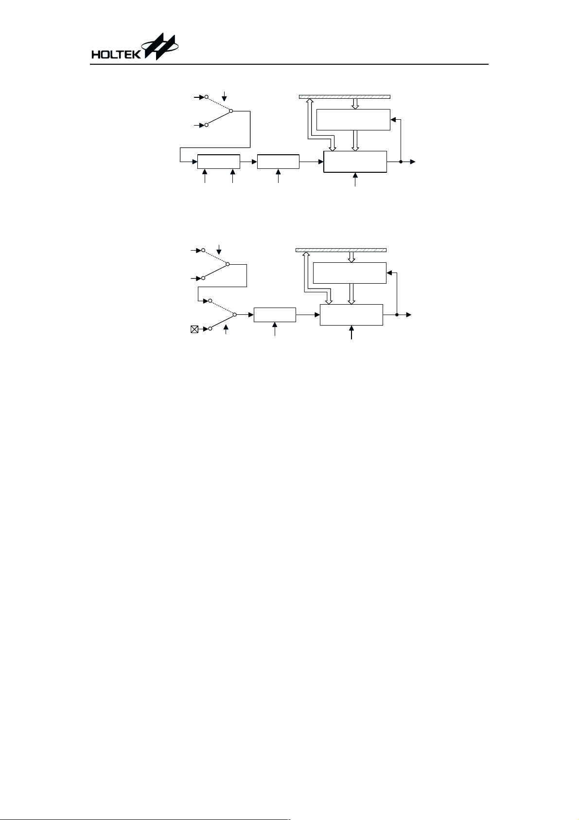
LCD Driver
HT9580
LC D _A0
LC D _C S 0 (M aster)
D0~D7
H T9580
LC D _E
LCD_RW
LCD_CL
5
3
2
15~8
7
6
4
A0
CS (Master)
C S (S lave)LC D _C S 1 (S lave)
D0~D7
SE D 15X (KS X )
E
R/W
CL
Master
Slave
T h e a p p lic a tio n c irc u it w h e n b it " L C D -C H IP 1 " = 0 a n d " L C D -C H IP 0 " = 0
LC D D river
LCD_A0
LC D _C S 0 (M aster)
LC D _C S 1 (S lave)
H T 9580
D0~D7
LCD_E
LCD_RW
LCD_CL
5
3
2
15~8
7
6
4
D/C
CE (M aster)
C E (S lave)
D0~D7
M C141X
CS
R/W
OSC2
Master
Slave
The application circuit w hen bit "LC D -CH IP 1" = 0 and "LC D -C H IP 0" = 1
24 April 28, 2000

Preliminary
LCD Driver
LCD_A0
LC D _C S 0 (M aster)
H T9580
D0~D7
LCD_E
LCD_RW
LCD_CL
5
3
2
15~8
7
6
4
RS
CS (M aster)
C S (S lave)LC D _C S 1 (S lave)
D0~D7
H D 66410
RD
WR
CR
The application circuit w hen bit "LC D -C H IP 1" = 1 and "LC D -C H IP0" = 0
LCD Driver Chip Selection Application Note
SEDX(EPSON) series LCD
driver at 68 family MPU appli
LCD-CHIP0="0"
LCD-CHIP1="0"
cation mode.
KSX(SAMSUNG) series LCD
driver at 68 family MPU appli
cation mode.
LCD-CHIP0="1"
LCD-CHIP1="0"
MC14X(MOTOROLA) series
LCD driver.
HD66410(HITACHI) series
LCD driver.
SEDX(EPSON) series LCD
LCD-CHIP0="0"
LCD-CHIP1="1"
driver at 80 family MPU
application mode.
KSX(SAMSUNG) series LCD
driver at 80 family MPU appli-
cation.
LCD-CHIP0="1"
LCD-CHIP1="1"
N/A
Master
RESET is low active
-
Pin options set as 68 family
MPU application mode.
Slave
RESET is high active
Pin options set as 80 family
MPU application mode.
HT9580
Power down operation - HALT
The HALT mode is initiated by setting the con
figuration register bit HALT high and results in
the following ...
The system clock turns off, the low power pager
sub-clock, LCD driver, pager decoder and RTC
all keep running.
The contents of the on-chip RAM and of the reg
ister remain unchanged.
As the WDT and the WDT prescaler depend on
software control, the WDT will continue to
count when the ²HALT² bit is set high.
All the I/O ports remain in their original status.
25 April 28, 2000
-

Preliminary
HT9580
D/A registers
Address
002FH D/A-L DA7 DA6 DA5 DA4 DA3 DA2 DA1 DA0 0000 0000
0030H D/A-H XXXXXD/A_PD RSSI BAT uuuu u1uu
Register
Name
Bit 7 Bit 6 Bit 5 Bit 4 Bit 3 Bit 2 Bit 1 Bit 0
State on
POR
The system can quit the HALT mode by an ex
ternal reset, an interrupt, an external falling
edge signal on port A or an RTC time out.
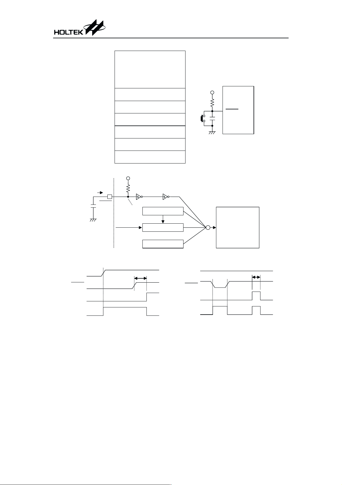
The HT9580 has one internal 8-bit D/A con
verter which can measure the battery voltage
and the RSSI input signal from the IF of the RF
circuit. The DA0~DA7 is the digital input of the
D/A converter and the analog outputs to the pin
named DA_OUT. Bit BAT of the DA-H register
(0030H) is the output of the comparator. Its in
put at the ²-² terminal is from the D/A output
and the ²+² terminal comes from the input pin
V
DD
D/A_PD
VDD (D/A) DA7
VSS
BAF
-
. The bit RSSI of DA-H register (0030H) is
the output of another comparator. Its input at
²-² terminal is from the D/A output and ²+² ter
minal comes from the input pin RSSI. The soft
ware can detect the battery voltage and the
RSSI signal by writing to the bits DA0 ~DA7
(002FH) and reading the bits BAT, RSSI (0030H).
Bit ²D/A_PD² is used for the D/A power down
control. If this bit islogic high, the D/Awill be in
-
the power down mode. Otherwise, the D/A is in
the normal condition. For details see the follow
ing figure.
RSSI
BAT
DA6
DA5
DA4
DA3
DA2
DA1
DA0
2R
R
2R
R
2R
R
2R
R
2R
R
2R
R
2R
R
2R
2R
RSSI
BAT
DA_OUT
-
-
-
The configuration of the 8-bit D /A converter and pow er dow n control
26 April 28, 2000

Buffer status register
Address
0031H
Register
Name
Buffer
Status
MSG_END X count_5 count_4 count_3 count_2 count_1 count_0 0uuu uuuu
Preliminary
Bit 7 Bit 6 Bit 5 Bit 4 Bit 3 Bit 2 Bit 1 Bit 0
HT9580
State on
POR
The buffer status register will relay to the mC
the status of the message buffer when the data
ready request interrupt occurred. The
²MSG_END² bit will be set high when the data
(including address codeword and message code
word) is at the end of this data ready interrupt
call. The valid data length of the message buffer
is determined by bit count_0 to count_5. If
²MSG_END² is low, the data length is more
0040H
0041H
0042H
0053H
0054H
0055H
006D H
Address C odew ord
M essage C odew ord 1
M essage C odew ord 2
M essage C odew ord 19
M essage C odew ord 20
than 46 or data is not at the end, the mC should
wait for the next data ready interrupt until the
bit ²MSG_END² is set high. Example 1: if the
data read from 0031H is ²95H² when a new
-
data ready interrupt occurred, it means the to
tal data length is 21 including the address code
word in this call and the message is terminated
(bit ²MSG_END² =1). The figure below illus
trates example 1.
M essage B uffer
N/A
N/A
-
-
-
B it7 B it6 B it5 B it4 B it3 B it2 B it1 B it0
00101 011
Example 1
27 April 28, 2000
0031H

Preliminary
HT9580
Example 2: if the data read from 0031H is
²2EH² when a new data ready interrupt oc
curred, that means thedata length of this call is
more than 46 and the next data ready interrupt
will occur. If the next interrupt occurs and the
contents of 0031H is ²85H², the result are
M essage B uffer
0040H
0041H
0042H
006C H
006D H 006D H
B it7 B it6 B it5 B it4 B it3 B it2 B it1 B it0
Address C odew ord
M essage C odew ord 1
M essage C odew ord 2
M essage C odew ord 44
M essage C odew ord 45
01010101
0031H
shown in the following figure. The programmer
should note that the information on the mes
sage buffer must be read out before the next
continuous codeword arrives. Otherwise the
data on the message will be overwritten.
M essage B uffer
M essage C odew ord 46
0040H
M essage C odew ord 47
0041H
M essage C odew ord 48
0042H
M essage C odew ord 49
0043H
M essage C odew ord 50
0044H
0045H
B it7 B it6 B it5 B it4 B it3 B it2 B it1 B it0
00 01
1010
N/A
N/A
0031H
-
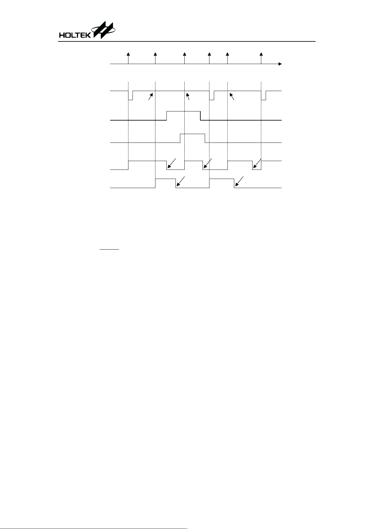
1st D ata R eady Interrupt
Example 2
The data ready interrupt will generate when
message is terminated, synchronization code
POCSAG DATA
Structure
NMI
DR_FG
M essage B uffer
(46 bytes)
Fram e5
DI
Fram e6 Fram e7 Fram e0 F ram e1 F ram e2
The timing chart of message buffer
2nd D ata R eady Interrupt
word is received or buffer is full. The following
figure will show the typical operation.
Sync
Valid Data
28 April 28, 2000

Preliminary
HT9580
SPI configure register
Address
0032H SPI-CONFIG S/M LEN1 LEN0 REQST SPIFG CLK_EDG SPI_EN START 0111 1000
Register
Name
Bit7 Bit6 Bit5 Bit4 Bit3 Bit2 Bit1 Bit0
State on
POR
·
S/M: Slave/master mode selection
When S/M is "0", HT9580 is in the master
mode. Otherwise, HT9580 is in the slave
mode.
01
S/M
·
LEN0, LEN1: Data length
Master mode
(SCK is output)
Slave mode
(SCK is input)
The LEN0 and LEN1 will determine the data
length between exchange.
LEN1 LEN0 Data Length (Bit)
00 4
01 8
10 16
11 32
·
REQST: SPI request (read only)
When FLEX
TM
decoder wants to exchange
data with HT9580, the REQST will have low
pulse.
·
SPIFG: SPI complete flag
0 (clear): Data transfer to external device has
been completed.
1 (set): No valid completion of data transfer.
The bit is cleared by hardware and set
by software.
·
CLK_EDG: Data sampling edge
The CLK_EDG will determine the valid
MISO and MOSI sampling edge of SCK clock.
01
CLK_EDG Rising edge Falling edge
·
SPI_EN: The SPI enable
01
When the SPI cir
cuit is disabled, the
SPI_EN
POCSAG decoder
I/O pins will be en
abled
·
START: The data exchange start or not
The SPI cir
cuit and SPI
I/O pins will
be enabled
01
Data
START No data exchange
exchange
start
When the bit is set by software, the SPI data
exchange will start. After the first bit data exchange is completed, the START bit will clear
to low again by hardware.
-
29 April 28, 2000

Preliminary
HT9580
SPI SPEED register (write only)
Address
0033H SPI-SPEED SP7 SP6 SP5 SP4 SP3 SP2 SP1 SP0 0000 0000
Register
Name
Bit7 Bit6 Bit5 Bit4 Bit3 Bit2 Bit1 Bit0
State on
POR
The register will determine the SCK clock frequency of SPI. When SPEED register are 00H, the SCK
clock output is high. The value of the frequency divider, ranging from 1 (SPEED=01H)~255
(SPEED=FFH). If SPEED=00H, the SCK output will be disabled.
X1-clock
8-bit S P E E D C ounter
SPI Control
SCK
SPI
SPI output buffer register (write only)
Address
0034H SPI-OUT3 D7 D6 D5 D4 D3 D2 D1 D0 0000 0000
0035H SPI-OUT2 D7 D6 D5 D4 D3 D2 D1 D0 0000 0000
0036H SPI-OUT1 D7 D6 D5 D4 D3 D2 D1 D0 0000 0000
0037H SPI-OUT0 D7 D6 D5 D4 D3 D2 D1 D0 0000 0000
Register
Name
Bit7 Bit6 Bit5 Bit4 Bit3 Bit2 Bit1 Bit0
State on
POR
The SPI-OUT3~0 are used when transmitting data on the serial bus. Only valid datawrite to the reg
ister SPI-OUT3~0 and "START" initiating will begin the SPI data transmission from HT9580 to
TM
FLEX
decoder. After completion of the 4-byte data transfer, the "SPIFG" status bit will be set and
the internal signal ²REQST² will generate a falling edge signal for NMI. The bit7 of SPI-OUT3 is
MSB and bit0 of SPI-OUT0 is LSB.
SPIFG
REQST
(N M I)
REQST
(register)
START
(register)
(from H T 9580)
(from decoder)
SCK
MOSI
MISO
Logic H igh
SPI-OU T3~0
SPI-IN 3~0
MSB
MSB
2
2
1
1
LSB
LSB
-
SS (to decoder)
SRDY
(from decoder)
SPI packet exchange initiated by the H T 9580
30 April 28, 2000

Preliminary
HT9580
SPI input buffer register (read only)
Address
0038H SPI-IN3 D7 D6 D5 D4 D3 D2 D1 D0 0000 0000
0039H SPI-IN2 D7 D6 D5 D4 D3 D2 D1 D0 0000 0000
003AH SPI-IN1 D7 D6 D5 D4 D3 D2 D1 D0 0000 0000
003BH SPI-IN0 D7 D6 D5 D4 D3 D2 D1 D0 0000 0000
Register
Name
Bit7 Bit6 Bit5 Bit4 Bit3 Bit2 Bit1 Bit0
State on
POR
The SPI-IN3~0 are used when receiving data on the serial bus. When SPI transmits only valid data
writes to the register SPI-OUT3~0, "START" will initiate the SPI data transmission from HT9580 to
TM
FLEX
decoder. After completion of the 4-byte data transfer, the "SPIFG" status bit will be set and
the internal signal "REQST" will generate a falling edge signal for NMI. The bit7 of SPI-IN3 is MSB
and bit0 of SPI-IN0 is LSB.
SPIFG
REQST
(N M I)
REQST
(register)
START
(register)
SCK
MISO
(from decoder)
MOSI
(from H T 9580)
SS (to decoder)
SRDY
(from decoder)
S P I-IN 3 ~ 0
SPI-OU T3~0
MSB
MSB
2
2
1
1
LSB
LSB
SPI packet exchange initiated by the H T 9580
31 April 28, 2000

Preliminary
HT9580
The POCSAG paging code
A transmission using the ²CCIR Radio paging
Code No.1² (POCSAG code) is generated in ac
PREAM BLE
1 0 1 0 .........1 0 1 0 1 0 1 0 1 0
Bit Num ber 1
A ddress codew ord
M essage codew ord
Id le c o d e w o rd
S y n c h c o d e w o rd
BATCH1 BATCH2 LAST BATCH
Synch CW CW
FRAM E0 FR AM E1 FRAM E7
2 to 19 20/21 22 to 31
18 A ddress B its
0
1
0
0
20 M essage Bits
POCSAG code structure
The transmission is started by sending a pre
amble, consisting of at least 576 continuously
alternating bits (10101010...). The preamble is
followed by an arbitrary number of batch
blocks. Only complete batches are transmitted.
Each batch comprises 17 code-words of 32 bits
each. The first code-word is a synchronization
code-word with fixed pattern. The sync word is
followed by 8 frames (0~7) of 2 code-words each,
containing message information. A code-word
in a frame can either be an address, message or
idle code-word.
Idle code-words also have fixed patterns and
are used to fill empty frames or separate messages.
cordance with the following rules (see the fol
lowing Figure).
-
CWCW CW CW
32
2 F unction
31 Idle code Bit pattern
31 S ynch code Bit pattern
Address code-words are identified by an MSB of
-
Bits
10 C R C bits
10 C R C bits
P
P
logic 0 and are coded as shown in the POCSAG
code structure figure. A user address or RIC
(Receiver Identity Code) consists of 21 bits.
Only the upper 18 bits are encoded in the address code-word (bits 2 to 19). The lower 3 bits
designate the frame number in which the address is transmitted.
Four different call types can be distinguished
on each user address. The call type is determined by two functional bits in the address
code-word (bits 20 and 21). The POCSAG standard recommends the use (in Taiwan) of combinations of data formats and function bits, as
shown in the following table. Other combina
tions will be set by SPF16~SPF19.
-
-
Bit 20 (MSB) Bit 21 (LSB) Call Type Data Format
0 0 Numeric 4-bit package
0 1 Alert only
1 0 Alert only
¾
¾
1 1 Alpha-numeric 7-bit package
Data formats and function bits
32 April 28, 2000

Preliminary
HT9580
Alert-only calls consist of a single address
code-word. Numeric and alphanumeric calls
have message code-words following the address.
Message code-words are identified by an MSB
of logic 1. The message information is stored in
a 20-bit field (bits 2 to 21). The data format is
determined by the call type: 4 bits per digit for
numeric message and 7 bits per (ASCII) charac
ter for alphanumeric messages. Each
code-word is protected against transmission er
rors by 10 CRC check bits (bit 22 to 31) and an
even parity bit (bit 32).
This permits correction of a maximum of 2 ran
dom errors or up to 4 errors in a burst of 4 bits
(a 4-bit burst error) per code-word.
·
Error correction
Item Description
Address
code-word
Message
code-word
two random errors, or 4-bit
burst errors (optional)
two random errors, or 4-bit
burst errors (optional)
Error correction
In the HT9580, error correction methods have
been implemented as shown in the table above.
Random error correction is the default for
both address and message code-word. In another method, burst error correction can be
switched by SPF programming. Up to 4 erroneous bits in a 4-bit burst can be corrected.
The error type detected for each code-word is
identified in the message data output to the
microcontroller, allowing rejection of calls with
too many errors.
·
Operating states
¨
ON status
¨
STANDBY status
The operating state is determined by control
address (0019H) bit 0 and monitored by bit 3
of address (0019H).
Truth table for decoder operating status
ON Input Operating Status
0 On state
1 STANDBY state
·
On status
In the ON status, the decoder pulses the re
ceiver, quick charge and PLL enable outputs
(respectively BS1, BS2 and BS3) according to
the code structure and the synchronization
algorithm. Data received serially at the data
input (DI) is processed for call receipt.
-
·
STB status
-
In the STB status the decoder will neither ac
tivate the receiver, quick charge or PLL en
-
able outputs, nor process any data at the data
input. The crystal oscillator remains active to
-
permit communication with the microcontroller.
·
Battery saving
Current consumption is reduced by switching
the STB internal decoder sections whenever
the receiver is not enabled. To further increase
battery efficiency, reception and decoding of an
address code-word is stopped as soon as the un
corrected address field differs by more than
3-bits from the enabled RICs. If the next
code-word has to be received again, the receiver
is re-enabled, thus observing the programmed
establishment times t
·
Data reception and buffer
BS1,tBS2
and t
BS3
.
Reception of a valid paging call is signaled to
the microcontroller by means of an interrupt
signal. The received address and message
code-word can then be read via a 46 bytes
message buffer (from 0040H to 006DH) fordecoder data message. If the mC did not read the
previous message within one code-word time
from the message buffer, the message buffer
data will be overwritten.
·
Bit rates
The HT9580 can be configured for data rates
of 512, 1200 or 2400 bit/s by SPF program
ming. These data rates are derived from
32.768kHz, 76.8kHz or 153.6kHz oscillator
frequencies.
·
Input data processing
The input data is noise filtered by means of a
digital filter. Data is sampled at 16 times the
data rate and averaged by majority decision.
33 April 28, 2000

Preliminary
HT9580
The filtered data is used to synchronize an in
ternal clock generator by monitoring transi
tions. The recovered clock phase can be
adjusted in steps of 1/8, 3/32, 1/16, or 1/32 bit
period per received bit.
All step size are used when bit synchroniza
tion has not been achieved, the smallest when
a valid data sequence has been detected.
·
Erroneous code-words
Upon receipt of erroneous uncorrectable
code-words, call termination occurs according
to the conditions given below:
SPF08 SPF09 Description
Any two consecutive
code-words or the
0X
code-word directly following
the address code-word in
error
1 0 Any single code-word in error
11
Any two consecutive
code-words in error
·
-
-
Message receiving mode
The receiving message mode (numeric or al
pha-numeric) depends on bits SPF16~SPF19.
If one of these bits from SPF16~SPF19 is
cleared to low, the decoder will be in numeric
-
package receiving mode. Otherwise, the de
coder is in the alphanumeric receiving mode.
An example is shown below:
SPF16=0
SPF17=0
SPF18=1
SPF19=1
Function Bits
Bit 20 (MSB) Bit 21 (LSB)
00
01
10
11
Message Re
ceiving Format
Numeric (4-bit)
Numeric (4-bit)
Alphanumeric
(7-bit)
Alphanumeric
(7-bit)
The decoder data output format is deter
mined by the value SPF16~SPF19. When it is
logic low, the 4-bit (numeric) package will be
selected. Otherwise, the 7-bit (alphanumeric)
package is selected. The following tables illus
trate the above two different conditions.
Message code-word on the message buffer (numeric receiving mode)
Bit7 Bit6 Bit5 Bit4 Bit3 Bit2 Bit1 Bit0
Error Flag 0 0 0 D3 D2 D1 D0
-
-
-
-
-
Message code-word on the message buffer (alphanumeric receiving mode)
Bit7 Bit6 Bit5 Bit4 Bit3 Bit2 Bit1 Bit0
Error Flag D6 D5 D4 D3 D2 D1 D0
·
Synch word indication
The synch word recognized by the HT9580 is
the standard POCSAG synchronization
code-word as shown in the following table.
BitNo.0123456789101112131415
Bit 0111110011010010
Bit No. 16 17 18 19 20 21 22 23 24 25 26 27 28 29 30 31
Bit 0001010111011000
34 April 28, 2000

Preliminary
·
Idle word indication
The idle word recognized by the HT9580 is a
standard POCSAG idle code-word as shown
in the following table.
HT9580
BitNo.0123456789101112131415
Bit 0111101010001001
Bit No. 16 17 18 19 20 21 22 23 24 25 26 27 28 29 30 31
Bit 1100000110010111
·
Error indication
After error correction, any code-word contain
ing more than 2-bit random errors or 4-bit
burst errors (option) in the address or mes
sage code-word may be indicated from the er
ror flag position.
·
Decoder and mC interface
The HT9580 has two mC interface available.
Bit 4Bit 5
DR_FG
(0006 H )
BF_FG
(0006 H )
Bit 7 Bit 6 Bit 5 Bit 4 B it 3 B it 2 B it 1 B it 0
BL OR RES ON
-
-
-
One is the pager control address (0019H),
which controls the operation and configura
tion of the decoder. The other is the pager
message buffer address (from 0040H to
006DH), which receives the message data of
calls in the parallel mode. The data ready
(DR_FG) and battery fail (BF_FG) interrupt
flags are in the interrupt flag register
(0006H).
0019 H
STB
-
Bit 0
C(NMI)
m
C PA7
m
(W ake up)
Bit 1
Bit 2
Bit 3
Bit 4
Bit 5
Bit 6
Bit 7
M essage Buffer
(46 B ytes)
PO C SA G Decoder
D ecoder D ata O utput
D ata R eady Interrupt
SPI REQ ST
1
Pager S ystem C LK
D ebounce
Circuit
VIL=0.9V
=1.0V
V
IH
DI
BAL
RF
BS1
CKT.
BS2
BS3
RSSI
B A F ( B a tte r y F a il In te r ru p t)
Note: The valueof 0019H-bit3 STB is set whendecoder enters the standby mode andcleared when de
coder enters the ON
The value of 0006H-bit4 BF_FG is dependent on the BAF
The value of 0019H-bit5 OR
The value of 0019H-bit6 BL
mode.
pin ststus.
is always changed by an out of range signal.
is cleared 0" by the decoder Battery low signal and set 1" when
the mC sets this bit high.
The value of 0006H-bit5 DR_FG is set 1" by the decoder Data-Ready interrupt signal and
cleared ²0² when the mC clears DR_FG.
35 April 28, 2000
-

Preliminary
HT9580
The decoder control address (0019H) contains a
battery low flag (BL
decoder standby flag (STB), a decoder software
reset (RES
(ON
the interrupt flag register (0006H). It not only
records the status information but controls the
operation of the decoder.
If the flag status of the battery fail (BF_FG)
changes from ²0² to ²1², the following condi
tions occur.
¨
The pager controller generates an interrupt
if thevalue of the data ready interrupt is ²0².
¨
The pager controller does not generate any
interrupt and no data is transmitted to it if
the value of the data ready interrupt is ²1².
INT flag register (0006H)
Symbol Bit R/W Description
BF_FG 4 R
DR_FG 5 R/W
), and a decoder on/off control bit
). The data ready and battery fail flag are in
), an out of range flag (OR),
-
Battery fail indication bit
Once the decoder detects that the battery fail condition occurred,
the BF_FG will go high.
Data ready interrupt indication bit
When a valid call is detected, data transfers to the message
buffer. The DR_FG bit goes high when the message is terminated
within 46 bytes, one batch is at the end during the message receiving or the data buffer is full if the data length is more than 46
bytes. The mC software should read the data on the message
buffer within one POCSAG message codeword (32-bit) time. The
mC software has to clear the DR_FG bit low.
On the other hand, if the status of the battery
fail flag (BF_FG) changes from ²1² to ²0², the
internal node PA.7 of the pager controller will
supply a wake-up function. After the decoder
asserts the data ready request, the data ready
interrupt is generated and the DR_FG bit (bit
5 of 0006H) isset high; then the data ready in
terrupt subroutine runs to process the call
data on the message buffer and resets the
DR_FG bit low.
The functional bits (ON
bits ( STB, OR
all used to control the status of the decoder
which is operated through the pager control
address as described in the following table.
-
, RES) and indication
,BL, BF_FG and DR_FG) are
Decoder control register (0019H)
Symbol Bit R/W Description
On/Off control bit
or STANDBY state of the decoder
bit low and then high after the pager
ON
RES
0 R/W
1 R/W
This bit selects the ON
0: ON state
1: STANDBY RES
If SPI circuit is enabled, it would be better if this bit is set high to
reduce power consumption.
Resets the decoder core output
The mC has to set the RES
controller is turned on.
The reset status must be released before writing data to the de
coder configuration RAM.
36 April 28, 2000
-

Preliminary
Symbol Bit R/W Description
Standby indication bit
STB 3 R
OR
BL
5R
6 R/W
When the value of the ON
STANDBY state. The STANDBY state allows the mC to execute
the configuration RAM setting.
Out-of-range indication bit
Whenever the decoder detects an out-of-range hold time, that is
selected by the configuration registers SPF06 and SPF07. The
out-of-range indication may be tested for an out-of-range condi
tion whenever the interface enable of the decoder is active; other
wise OR
detection of valid data transmission.
If the out-of-range indication bit changes the status from high to
low or low to high, an interrupt will be generated and the
out-of-range hold-off time-out counter starts to count.
The bit is not valid when the SPI circuit is enabled.
Battery low indication bit
The battery low indication is periodically tested for a battery low
condition. If the decoder encounters a battery low condition, the
battery low indication bit is cleared low. The mC can only set the
BL
The bit is not valid when the SPI circuit is enabled.
is normally low. The out-of-range indication is set high by
bit high. Attempting to clear this bit has no effect.
bit is 1, the system goes into the
HT9580
-
-
·
User address format
A user address in the POCSAG code consists
of 21 bits. Three of the 21 bits are coded in the
frame number and are therefore not explicitly
transmitted. In the decoder, the addresses A,
B, C, D, E and F can use six different frames
respectively. Every address has to be explicitly enabled by resetting the associated enable bit.
Example:
Address decimal value: RICA=10535
Binary equivalent (14-bit): 10100100100111
Binary equivalent (18+3-bit):
000000010100100100111
Register allocation
A00 A01 A02 A03 A04 A05 A06
0000000
A07 A08 A09 A10 A11 A12 A13
1010010
A14 A15 A16 A17 FA2 FA1 FA0
0100111
37 April 28, 2000

Preliminary
HT9580
·
Test mode
The test mode of the decoder is selected by set
ting the TS
mode, the RF control outputs BS1 and BS3 are
constantly set high, but BS2is set low. After the
TS
pin is set high the decoder exits the test
mode.
·
Message data transfer
The decoder outputs a deformatted address
word and message words upon receipt of a valid
call. The message data to be transferred is or
ganized into 8-bit words and transferred to the
message buffer address (0040H to 006DH). The
data ready interrupt flag will be set high when
·
Address word format
Bit7 Bit6 Bit5 Bit4 Bit3 Bit2 Bit1 Bit0
Sync. State Call Address Dup. Call Valid Address Function Code
Note: Bit0: Bit21 of the address code-word
Bit6 Bit5 Bit4 Call Address
0 0 0 RIC A
0 0 1 RIC B
0 1 0 RIC C
0 1 1 RIC D
1 0 0 RIC E
1 0 1 RIC F
11 0
11 1
pin low at any time. In the test
Bit1: bit20 of the address code-word
Bit2: If this bit is ²1², the address word is valid, oterwise the address word is not valid.
Bit3: 1 for a duplicate code-word
Bit7: 1 if an address code-word is received in the data fail mode
¾
¾
-
-
the received data (including address code
word and message codeword) length is ter
minated within 46 bytes, one batch is over
or if the 46 bytes data buffer is full if data
length is more than 46 bytes. If the data in
the message buffer is terminated, the
²MSG_END² (0031H) bit will set high.
The address word indicates call address,
functional bit setting, and decoder flags. The
message code-words are received and con
catenated to a valid call address word. The
message words are derived from un-cor
rected message code-words.
·
Interrupt indication
The HT9580 provides an internal data ready
interrupt and a battery fail interrupt. The internal data ready interrupt and battery fail
interrupt share the NMI location. Which interrupt occurred can be determined by checking the battery fail interrupt bit (BF_FG; bit 4
of 0006H) and the data ready interrupt bit
(DR_FG; bit 5 of 0006H). Both interrupt bits
are active high.
-
-
-
-
38 April 28, 2000

Preliminary
·
Out-of-range indication
The out-of-range condition occurs when the
time interval defined by SPF06, SPF07 is un
able to receive sync code words. If sync code
words are detected, the timer counter defined
by SPF06, SPF07 will reset. This signal will
be seen as a loss of RF signal indication and
the power on reset is in an out-of-range condi
tion until the sync code word is detected.
·
Duplicate call suppression
The HT9580 provides a duplicate call sup
pression with time-out facility, to identify du
plicate call reception. In the display pager
mode, duplicate call indication is achieved
only via the mC interface. A call is assumed to
be a duplicate if its latest address and func
tion bit setting is equal to the previous re
ceived call within the time interval defined by
SPF06, SPF07.
·
Receiver, Quick charge and PLL signal control
Pager receiver, quick charge circuit, and RF
PLL circuit can be controlled independently
via enable outputs BS1, BS2, and BS3 respec
tively. Their operating period are optimized
according to the synchronization mode of the
decoder. Each enable signal has its own programmable establishment time.
HT9580
Receiver Establishment
Time T
512 bps 1200/2400 bps SPF00 SPF01
BS1
7.81ms 53.33ms 0 0
15.63ms 6.67ms 0 1
-
31.25ms 13.33ms 1 0
62.50ms 26.67ms 1 1
-
-
Quick Charge
Adjustment Time T
BS2
512 bps 1200/2400 bps SPF02 SPF03
7.81ms 1.67ms 0 0
-
-
15.63ms 6.67ms 0 1
15.63ms 11.67ms 1 0
19.53ms 13.33ms 1 1
PLL Establishment Time
T
BS3
-
512 bps 1200/2400 bps SPF04 SPF05
0ms 0ms 0 0
31.25ms 26.67ms 0 1
46.87ms 40.00ms 1 0
62.50ms 53.33ms 1 1
Option
Option
Option
R.F. timing chart
Data In
BS1
BS2
BS3
Data Bits
T
BS1
T
BS2
T
BS3
39 April 28, 2000

Preliminary
HT9580
Decoder configuration RAM
The decoder contains a 21-byte RAM to store six
user addresses, six frame numbers, and specially
programmed function bits (SPF00~SPF19) for
the decoder application configuration. The data
Address
001AH ENA
001BH A07 A08 A09 A10 A11 A12 A13 A14
001CH A15 A16 A17 FA2 FA1 FA0 X X
001DH ENB
001EH B07 B08 B09 B10 B11 B12 B13 B14
001FH B15 B16 B17 FB2 FB1 FB0 X X
0020H ENC
0021H C07 C08 C09 C10 C11 C12 C13 C14
0022H C15 C16 C17 FC2 FC1 FC0 X X
0023H END
0024H D07 D08 D09 D10 D11 D12 D13 D14
0025H D15 D16 D17 FD2 FD1 FD0 X X
0026H ENE
0027H E07 E08 E09 E10 E11 E12 E13 E14
0028H E15 E16 E17 FE2 FE1 FE0 X X
0029H ENF
002AH F07 F08 F09 F10 F11 F12 F13 F14
002BH F15 F16 F17 FF2 FF1 FF0 X X
002CH SPF00 SPF01 SPF02 SPF03 SPF04 SPF05 SPF06 SPF07
002DH SPF08 SPF09 SPF10 SPF11 SPF12 SPF13 SPF14 SPF15
002EH SPF16 SPF17 SPF18 SPF19 XXXX
Bit7 Bit6 Bit5 Bit4 Bit3 Bit2 Bit1 Bit0
A00 A01 A02 A03 A04 A05 A06
B00 B01 B02 B03 B04 B05 B06
C00 C01 C02 C03 C04 C05 C06
D00 D01 D02 D03 D04 D05 D06
E00 E01 E02 E03 E04 E05 E06
F00 F01 F02 F03 F04 F05 F06
memory is mapped to the address
001AH~002EH.
The configuration memory mapping table is
shown below.
Bit Definition
40 April 28, 2000

Preliminary
HT9580
Description of the special programmed
function bits (SPFn)
The following featurescan be selected by appro
priate programming of the specially pro
grammed function bits:
·
SPF00~SPF01
Receiver (BS1) establishment time (for the
BS2~BS3 options, refer to SPF02~SPF05)
00: 7.81ms/512 53.33ms/1200/2400
01: 15.63ms/512 6.67ms/1200/2400
10: 31.25ms/512 13.33ms/1200/2400
11: 62.50ms/512 26.67ms/1200/2400
Note: The recommendatory setting is 11.
·
SPF02~SPF03
RF dc level adjustment (BS2) enable time
00: 7.81ms/512 1.67ms/1200/2400
01: 11.71ms/512 6.67ms/1200/2400
10: 15.63ms/512 11.67ms/1200/2400
11: 19.53ms/512 13.33ms/1200/2400
·
SPF04~SPF05
PLL (BS3) establishment time
00: 0ms/512 0ms/1200/2400
01: 31.25ms/512 26.67ms/1200/2400
10: 46.87ms/512 40.00ms/1200/2400
11: 62.50ms/512 53.33ms/1200/2400
·
SPF06~SPF07
The duplicate call suppress time-out and
out-of-range hold-off time-out
00: 30s/512/1200 15s/2400
01: 60s/512/1200 30s/2400
10: 120s/512/1200 60s/2400
11: 240s/512/1200 120s/2400
·
SPF08~SPF09
0x: Any two consecutive code-words or the
code-word directly following the address
code-word in error
10: Any single code-word in error
11: Any two consecutive code-words in error
·
SPF10
1: 4-bit burst error correction for address and
-
-
message code-word
0: 2-bit random error correction for address
and message code-word
·
SPF11
1: Out-of-range Hold-off period according to
SPF06 and SPF07
0: Out-of-range Hold-off period is 0 regardless
of SPF06 and SPF07
Baud rate selection bits(SPF12,SPF13,SPF14)
SPF12 SPF13 SPF14
0 0 0 32768 512
0 0 1 76.8k 512
0 1 0 76.8k 1200
0 1 1 76.8k 2400
1 0 0 153.6k 512
1 0 1 153.6k 1200
1 1 0 153.6k 2400
Connected
Crystal (Hz)
Note: The (SPF12, SPF13, SPF14) = (0, 1, 0)
when power on reset
·
SPF15
Non-inverting or inverting data input selection
1: Inverting input selected for DI from RF circuit, referring to DI
0: Non-inverting input selected for DI from
RF circuit reserved, should be 0
·
SPF16~SPF19
Message receiving mode selection depending
on the function code (bit20, bit21)
01
SPF16 Function Code (0, 0) is
a numeric message
SPF17 Function Code (0, 1) is
a numeric message
SPF18 Function Code (1, 0) is
a numeric message
SPF19 Function Code (1, 1) is
a numeric message
Function Code (0, 0) is an
alpha-numeric message
Function Code (0, 1) is an
alpha-numeric message
Function Code (1, 0) is an
alpha-numeric message
Function Code (1, 1) is
analpha-numeric message
Baud Rate
(bps)
41 April 28, 2000

Preliminary
CPU Core
The HT9580 is a high performance pager con
troller specifically designed for use in new gen
eration radio pagers. It is based on the M6502
core. The 6502 Microprocessor offers complete
hardware and software capability with existing
6500 series of products aswell as significant en
hancements.
Instruction register and decoder
Instructions fetched from memory are gated
onto the internal bus. These instructions are
latched into the instruction register then de
coded, along with timing and interrupt signals,
to generate control signals for the various regis
ters.
Timing control unit
The timing control unit keeps track of the in
struction cycle being monitored. The unit is set
to 0 each time an instruction fetch is executed
and is advanced at the beginning of each input
clock pulse for as many cycles as required to
complete the instruction. Each data transfer
between registers depends upon decoding the
contents of both the Instruction Register and
the Timing Control Unit. There are three major
clocks in the mC as follows:
·
Phase 2 In (PHI2 (IN))
This signal is from the OSC1 input pin of
HT9580. The PHI1 (OUT) and PHI2 (OUT)
are derived from this signal.
·
Phase 2 Out (PHI2 (OUT))
This signal is generated from PHI2 (IN).
PHI2 (IN) provides the system timing. There
is a slight delay from PHI2 (IN).
·
Phase 1 Out (PHI1 (OUT))
Inverted PHI2 (OUT) signal. There is a slight
delay from PHIN2 (IN).
Read/write
This signal is normally in a high state indicat
ing that the mC is reading data from the data
bus memory. In the low state the data bus has
-
-
valid data from the mC to be stored at the ad
dressed memory location.
Parameter Description
-
-
-
-
t
cyc
t
ad
t
ah
t
dis
t
dih
t
dod
t
doh
t
denbd
t
wed
t
syd
t
syh
t
vd
t
vh
t
sos
t
soh
t
rds
t
rdh
t
ress
t
resh
Clock cycle time (min)
Address delay time
Address hold time
Read data in setup time
Read data in hold time
Write data out delay time
Write data out hold time
DATAEN delay time
WE_N delay time
SYNC delay time
SYNC hold time
VPB delay time
VPB hold time
SOB_N setup time
SOB_N hold time
RDY setup time
RDY hold time
RES_N setup time
RES_N hold time
Timing parameter annotations
Arithmetic and logic unit
All arithmetic and logic operations take place
within the ALU including incrementing and
decrementing internal registers (except for the
program counter). The ALU has no internal
memory and is used only to perform logical and
-
transient numerical operations.
HT9580
-
42 April 28, 2000

Preliminary
t
cyc
HT9580
CLK
ADD R
DATAI
DATAO
DATAEN
WE_N
SYNC,
VPB
RDY,
RES_N
SOB_N
t
ad
R D Address W R Address
t
dis
READ
t
dih
t
, t
syd
vd
t
, t
syh
vh
t
, t
, t
rd s
re ss
sos
t
t
t
t
ah
dod
t
wed
rd h
denbd
, t
re sh
WRITE
t
, t
soh
doh
M6502 read and write cycle
Accumulator
The Accumulator is a general purpose 8-bit register which stores the results of most arithmetic and logic operations. In addition, the
accumulator usually contains one of the two
data words used in these operations.
Index register
There are two 8-bit Index Register (X and Y)
which may be used to count program steps or to
provide an index value to be used in generating
an effective address. When executing an in
struction which specifies indexed addressing,
the mC fetches the opcode and the base address,
and modifies the address by adding the index
register to it prior to performing the desired op
eration. Pre- or post-indexing of indirect ad
dresses is possible.
Processor status register
The 8-bit processor status register contains
seven status flags. Some of the flags are controlled by the program, others may be controlled both by the program and the mC. The
HT9580 instruction set contains a number of
conditional branch instructions which are de
signed to allow testing of these flags.
Program counter
The 16-bit program counter register provides
-
the addresses which step the mC through se
quential program instructions. Each time the
HT9580 fetches an instruction from the pro
gram memory, the lower byte of the program
-
counter (PCL) is placed on the low-order bits of
-
the address bus and the higher byte of the pro
gram counter (PCH) is placed on the high-order
43 April 28, 2000
-
-
-
-

Preliminary
HT9580
8 bits. The counter is incremented each time an
instruction or data is fetched from the program
memory.
Stack pointer
The stack pointer is an 8-bit register which is
used to control the addressing of the vari
able-length stack. The stack pointer is auto
matically incremented and decremented under
control of the microprocessor to perform stack
manipulations under direction of either the
program or interrupt (NMI and IRQ). The stack
allows simple implementation of nested sub
routines and multiple level interrupts. The
stack pointer is initialized by the user¢s soft
ware.
70
70
70
158
PCH
15
0 0 0 0 0 0 0 1
70
70
Status register
NVEBD I ZC
Note: C: Carry 1=true
Z: Zero 1=true
-
-
I: IRQ
D: Decimal mode 1=true
1=disable
B: BRK command 1=BRK, 0=IRQ
E: Expansion bit (reserved)
V: Overflow 1=true
-
N: Negative 1=negative
-
A A ccum u la tor A
Y Index R egister Y
X Index R egister X
PC L P rogram C ounter PC
S S ta c k P o in te r
The w idth of the corresponding registers
44 April 28, 2000

Preliminary
Interrupt System
The HT9580 is capable of directly addressing
64 Kbytes of memory. The address space has
special significance within certain addressing
modes, as follows:
Reset and interrupt vectors
The reset and interrupt vectors use the major
ity of the fixed addresses between FFFA and
FFFF.
Stack
The stack may use memory from 01D0 to 01FF.
The effective address of stack and stackrelative
addressing modes will always be within this
range.
Interrupt request - IRQ
This CMOS compatible signal requests that an
interrupt sequence begin within the mC. The
IRQ is sampled during PHI2 operation; if the
interrupt flag in the processor status register is
0, the current instruction is completed and the
interrupt sequence begins during PHI1. The
program counter and processor status register
are stored in the stack. The mC will then set the
interrupt mask flag high so that no further interrupts may occur. At the end of this cycle, the
PCL will be loaded from address FFFE, and
PCH from location FFFF, transferring program
control to the memory vector located at these
addresses. The IRQ signal going low causes 3
bytes of information to be pushed onto the stack
before jumping to the interrupt handler. The
first byte is the high byte in the program coun
ter. The second byte is the program counter low
byte. The third byte is the status register value.
These values are used to return the processor to
its original state prior to the IRQ interrupt.
Non-maskable interrupt - NMI
A negative-going edge on this input requests
that a non-maskable interrupt sequence be
generated within the mC. The NMI is sampled
during PHI2; the current instruction is com
pleted and the interrupt sequence begins dur
ing PHI1. The Program Counter is loaded with
the interrupt vector from locations FFFA (low
byte) and FFFB (high byte), thereby transfer
ring program control to the non-maskable in
terrupt routine. The NMI is generated from
data ready interrupt or battery fail interrupt
flag (0006H). However, it should be noted that
this is an edge-sensitive input. As a result, an
-
other interrupt will occur if there is another
negative-going transition and the program has
not returned. Also, no interrupt will occur if
NMI is low and a negative-going edge has not
occurred since the last non-maskable interrupt.
The NMI signal going low causes 3 bytes of in
formation to be pushed onto the stack before
jumping to the interrupt handler. The first byte
is the high byte in the program counter. The
second byte is the program counter low byte.
The third byte is the status register value.
These values are used to return to its original
state prior to NMI interrupt.
Data address space
The mC internal address bus consistsof A0~A15
forming a 16-bit address bus for memory and
I/O exchanges on the data bus. The output of
each address line is CMOS compatible. The Address output pins of HT9580 (A0~A15) derive
from mC internal address pins A0~A15. The extended address pins (RA14~RA18) are the combination of bank point registers (0015H,
0016H) and internal address. The extended address pins are used to access internal/external
SRAM or Mask ROM (Character ROM).
The data lines constitute 8-bit bidirectional
-
data bus for use during exchanges between the
mC and peripherals. The outputs are
three-state buffers capable of driving CMOS
load. The Program Address and Data Address
space is continuous throughout the 64 Kbyte
address space. Words, arrays, records, or any
data structures may span the 64 Kbytes ad
dress space. The following addressing mode de
scriptions provide additional detail as to how
effective addresses are calculated. Fifteen ad
-
dressing modes are available for the HT9580 as
-
illustrated on the next page.
HT9580
-
-
-
-
-
-
-
45 April 28, 2000

Preliminary
HT9580
Addressing modes
The M6502 supports fifteen (15) addressing
modes, shown in table below. In interpreting
this table you should note that:
·
The byte following a 2 byte opcode = IAL (typ.)
·
The 2 bytes following a 3 byte opcode = BAL
and BAH (typ.)
·
Standard assembly notation is used
Mode Description
IMP
ACC
IMM
ZPG
ZPX
ZPY
ABS
ABX
ABY
ABI
AIX
IND
IMPLIED: The data is implied in the opcode (example: CLC)
ACCUMULATOR: The accumulator is used as the source data. (data=AREG)
IMMEDIATE: The byte following the opcode is the data. (data=IAL)
ZERO PAGE: The first 256 RAM locations (0000H~00FFH) are used for fast access
and small code size. The upper 8-bit of the address are always zero. [data=(00, IAL)]
ZERO PAGE INDIRECT X: The X register is added to the byte following the opcode to
give a new zero page address. Note that the upper 8-bit of the address are always zero.
[data=(00, IAL+X)]
ZERO PAGE INDIRECT Y: The Y register is added to the byte following the opcode to
give a new zero page address. Note that the upper 8-bit of the address are always zero.
Only the LDX and the STX opcodes use this mode. [data=(00, IAL+Y)]
ABSOLUTE: The two bytes following the opcode give the absolute address of the data.
[data=(BAH, BAL)]
ABSOLUTE X: The X register is added to the two bytes following the opcode to produce
a new 16-bit address. {data=[(BAH, BAL)]+X}
ABSOLUTE Y: The Y register is added to the two bytes following the opcode to produce
a new 16-bit address. {data=[(BAH, BAL)]+Y}
ABSOLUTE INDIRECT: The two bytes following the opcode are used as a pointer to
memory. Only the JMP opcode uses this mode. [data=(BAH, BAL)]
INDEXED ABSOLUTE INDIRECT X: The two bytes following the opcode are added to
the X register to yield a new 16-bit address. The contents of this address and the fol
lowing one are used as an indirect address. Only the JMP opcode uses this mode.
{data=[(BAH, BAL+X+1), (BAH, BAL+X)]}
INDIRECT: The byte following the opcode is used as a pointer to the zero page. The
contents of this address and the following one are used as the address to finally access
the data. {data=[(IAL+1), (IAL)]}
·
·
A number in parenthesis indicates that the
contents of the location pointed to by the
number are to be used. For example (12H) in
dicates the contents of address 12H.
A comma in the addressis used to indicate the
high and low byte of an address. For example
(01H, AAH) indicates the contents of address
01AAH.
-
-
46 April 28, 2000

Preliminary
Mode Description
INDIRECT X: The byte following the opcode is added to the X register to produce a new
zero page address. The contents of this address and the following one are used as the
INX
INY
REL
address to finally access the data. Note that when the X register is added to the byte
following the opcode, the upper byte of the address is always zero. {data=[(00,
IAL+X+1), (00, IAL+X)]}
INDIRECT Y: The byte following the opcode is a zero page address. The contents of
this location and the next one produce a 16-bit address which is then added to the Y
register to finally obtain the data. {data=<[(00, IAL+1), (00, IAL)]+Y>}
RELATIVE: The byte following the opcode is added in 2's complement fashion to the
PC. The byte is sign extended. Used by branching instructions.
HT9580
47 April 28, 2000

Preliminary
Application Circuits
OSC1, OSC2 require an external resistor
VDD (1 .5 V )
HT9580
LCD Display
Holtek
Pager
+
-
H T93LC 46
470mH
+
22mF
LCD Driver
EEPRO M
Schottky D iode
R H 5R 302
V
DD
VSS
SW 1
SW 2
SW 3
LX
CS
SK
DO
V
100k
0.1mF
DC/DC
VSS
MasterSlave
DI
DD
W
OUT
49
46
47
48
44
66
72
71
70
73
3V
+
22mF
1, 25, 56
LC D _E
D0~D7
LC D _R W
RESET
LC D _C S0 (M aster)
LC D _C S1 (Slave)
LC D _C L
LC D _A 0
PB4
PB1
PB2
PB3
PB0
PB5~PB7
PA3~PA5
TM R 1
TS
PA0
PA1
PA2
RESET
VDD
H T 9580
BS1
BS2
BS3
BAL
RSSI
BAF
BZ
DA_OUT
X2
X1
OSC1
OSC2
P_M OD E
D0~D7
A0~A15
PSEN
DI
1 .5 V
65
64
63
62
58
61
59
55
60
79
80
77
76
26
20
R eceiver
76.8kH z
V
DD
D0~D7
A0~A15
CE
OE
VDD
RF
VSS
510
W
0.1mF
Norm al Type
Rom less
H T27LC 512
Program R O M
1 .5 V
0.1mF
B uzze r
1k
W
Lam p
1 .5 V
680
Motor
53
PC0
54
PC1
1 .5 V
W
M
A0~A13
RA14~RA17
D0~D7 D0~D7
MASK_CE
SRAM _CE
VSS
27, 57, 78
A0~A17
18
ROM CE
17
RAMCE
16
R/W
OE
WE
19
OE
Note: The external m em ory is optional
M askR A M
48 April 28, 2000

Preliminary
HT9580
OSC1, OSC2 do not require a resistor. The OSC1 clock comes from an internal pad ²DF² only
VDD ( 1 .5 V )
Schottky Diode
H
470
LCD Display
Holtek
Pager
+
-
H T93LC 46
1k
W
Lam p
+
1 .5 V
m
22
F
m
R H 5R 302
LCD Driver
EEPRO M
VSS
SW 1
SW 2
SW 3
680
W
Motor
V
DD
LX
DC/DC
MasterSlave
CS
SK
DI
DO
V
DD
100k
0.1mF
M
VSS
1 .5 V
W
OUT
49
46
47
48
44
66
72
71
70
73
53
54
LC D _E
D0~D7
LC D _R W
RESET
LC D _C S0 (M aster)
LC D _C S1 (Slave)
LC D _C L
LC D _A 0
PB4
PB1
PB2
PB3
PB0
PB5~PB7
PA3~PA5
TM R 1
TS
PA0
PA1
PA2
RESET
PC0
PC1
+
22mF
3V
1, 25, 56
VDD
H T 9580
RA14~RA17
VSS
27, 57, 78
65
BS1
64
BS2
63
BS3
62
DI
58
BAL
61
RSSI
59
BAF
55
BZ
DA_OUT
P_M ODE
MASK_CE
SRAM _CE
60
79
X2
80
X1
DF 153.6kHz
OSC1
OSC2
26
D0~D7
A0~A15
20
PSEN
A0~A13
D0~D7 D0~D7
18
17
16
R/W
19
OE
N o te : T h e e x te rn a l m e m o r y is o p tio n a l
R eceiver
76.8kH z
V
DD
D0~D7
A0~A15
CE
OE
A0~A17
ROM CE
RAMCE
WE
OE
1 .5 V
VDD
RF
VSS
510
W
0.1
F
m
Norm al Type
Rom less
H T27LC 512
Program R O M
M a skR A M
1 .5 V
0.1
B uzze r
F
m
49 April 28, 2000

The SPI application circuits
VDD (1 .5 V )
Preliminary
HT9580
LC D D isplay
Holtek
Pager
+
-
H T93LC 46
470mH
+
22mF
LCD Driver
EEPRO M
Schottky Diode
R H 5R 302
V
DD
VSS
SW 1
SW 2
SW 3
LX
CS
SK
DO
V
100k
0.1mF
DC/DC
VSS
MasterSlave
DI
DD
W
OUT
49
46
47
48
44
66
72
71
70
73
3V
+
22mF
1 , 2 5 , 5 6
LC D _E
D0~D7
LC D _R W
RESET
LC D _C S0 (M aster)
LC D _C S1 (Slave)
LC D _C L
LC D _A 0
PB4
PB1
PB2
PB3
PB0
PB5~PB7
PA3~PA5
TM R 1
TS
PA0
PA1
PA2
RESET
VDD
H T 9580
SS
SCK
MOSI
MISO
SRDY
RSSI
BAF
BZ
DA_OUT
X2
X1
OSC1
OSC2
P_M ODE
D0~D7
A0~A15
PSEN
1 .5 V
1 .5 V
VDD
R eceiver
VSS
0.1mF
B uzze r
RF
65
64
63
62
58
61
59
55
60
79
76.8kH z
80
77
76
26
D0~D7
A0~A15
20
CE
OE
Flex
Decoder
510
W
0.1mF
V
DD
Norm al Type
Rom less
TM
H T27LC 512
Program R O M
1k
W
Lam p
1 .5 V
680
Motor
53
PC0
54
PC1
1 .5 V
W
M
A0~A13
R A 14~R A 17
D0~D7 D0~D7
MASK_CE
SRAM _CE
VSS
27, 57, 78
A0~A17
18
ROM CE
17
RAMCE
16
R/W
OE
WE
19
OE
Note: The external m em ory is optional
M a skR A M
50 April 28, 2000

Preliminary
HT9580
Detailed Instruction Operation
The table below provides a brief description of each opcode.
The first column lists the name or the assembler mnemonic for the instruction.
The second column lists the opcode in hexadecimal.
The third column lists the address mode for the instruction.
The flags column indicates which of the 8-bit of flags are updated by the instruction.
Legend:
-®No change
+
6
7
The number of bytes column gives the number of bytes for the opcode.
The number of cycles column gives the number of clock cycles for the opcode. (A+b indicates one addi
tional cycle when a branch is taken within the same page, or 2 cycles if the branch is to a different
page.)
The last column are the description or brief descriptions of the opcode.
The operator notation is as follows:
=> assignment
+
- 2¢s complement subtract
| Bitwise OR
& Bitwise AND
^ Bitwise exclusive OR
!
<< Left rotate
>> Right rotate
< Left shift
> Right shift
A Accumulator
C Carry flag
X X index register
Y Y index register
S Stack pointer
M Memory
® Updated
® From memory bit 6
® From memory bit 7
2¢s complement add
Bitwise invert (one¢s complement)
-
51 April 28, 2000

Preliminary
HT9580
Name Opcode
ADC 69 IMM ++----++ 2 2 A+M+C=>A, C Add with carry
ADC 65 ZPG ++----++ 2 3 A+M+C=>A, C Add with carry
ADC 75 ZPX ++----++ 2 4 A+M+C=>A, C Add with carry
ADC 6D ABS ++----++ 3 4 A+M+C=>A, C Add with carry
ADC 7D ABX ++----++ 3 4 A+M+C=>A, C Add with carry
ADC 79 ABY ++----++ 3 4 A+M+C=>A, C Add with carry
ADC 72 IND ++----++ 2 5 A+M+C=>A, C Add with carry
ADC 61 IDX ++----++ 2 6 A+M+C=>A, C Add with carry
ADC 71 IDY ++----++ 2 5 A+M+C=>A, C Add with carry
AND 29 IMM +-----+- 2 2 A&M=>A AND A with M
AND 25 ZPG +-----+- 2 3 A&M=>A AND A with M
AND 35 ZPX +-----+- 2 4 A&M=>A AND A with M
AND 2D ABS +-----+- 3 4 A&M=>A AND A with M
AND 3D ABX +-----+- 3 4 A&M=>A AND A with M
AND 39 ABY +-----+- 3 4 A&M=>A AND A with M
AND 32 IND +-----+- 2 5 A&M=>A AND A with M
AND 21 IDX +-----+- 2 6 A&M=>A AND A with M
AND 31 IDY +-----+- 2 5 A&M=>A AND A with M
ASL 0A ACC +-----++ 1 2 A<1=>A shift left 1, C<-7, 0<-zero
ASL 06 ZPG +-----++ 2 5 M<1=>M shift left 1, C<-7, 0<-zero
ASL 16 ZPX +-----++ 2 6 M<1=>M shift left 1, C<-7, 0<-zero
ASL 0E ABS +-----++ 3 6 M<1=>M shift left 1, C<-7, 0<-zero
ASL 1E ABX +-----++ 3 7 M<1=>M shift left 1, C<-7, 0<-zero
BBR0 0F REL -------- 3 5+b IfM(0)=0, PC<=PC+Off (Off sign ext)
BBR1 1F REL -------- 3 5+b IfM(1)=0, PC<=PC+Off (Off sign ext)
BBR2 2F REL -------- 3 5+b IfM(2)=0, PC<=PC+Off (Off sign ext)
BBR3 3F REL -------- 3 5+b IfM(3)=0, PC<=PC+Off (Off sign ext)
BBR4 4F REL -------- 3 5+b IfM(4)=0, PC<=PC+Off (Off sign ext)
BBR5 5F REL -------- 3 5+b IfM(5)=0, PC<=PC+Off (Off sign ext)
BBR6 6F REL -------- 3 5+b IfM(6)=0, PC<=PC+Off (Off sign ext)
BBR7 7F REL -------- 3 5+b IfM(7)=0, PC<=PC+Off (Off sign ext)
BBS0 8F REL -------- 3 5+b IfM(0)=1, PC<=PC+Off (Off sign ext)
BBS1 9F REL -------- 3 5+b IfM(1)=1, PC<=PC+Off (Off sign ext)
BBS2 AF REL -------- 3 5+b IfM(2)=1, PC<=PC+Off (Off sign ext)
BBS3 BF REL -------- 3 5+b IfM(3)=1, PC<=PC+Off (Off sign ext)
BBS4 CF REL -------- 3 5+b IfM(4)=1, PC<=PC+Off (Off sign ext)
Addr
Mode
NVEBD I Z C
Flags
No.
Bytes
No.
Cyc.
Description
52 April 28, 2000

Preliminary
HT9580
Name Opcode
BBS5 DF REL -------- 3 5+b IfM(5)=1, PC<=PC+Off (Off sign ext)
BBS6 EF REL -------- 3 5+b IfM(6)=1, PC<=PC+Off (Off sign ext)
BBS7 FF REL -------- 3 5+b IfM(7)=1, PC<=PC+Off (Off sign ext)
BCC 90 REL -------- 2 2+b IfC=0, PC<=PC+M (Msign extended)
BCS B0 REL -------- 2 2+b IfC=1, PC<=PC+M (Msign extended)
BEQ F0 REL -------- 2 2+b IfZ=1, PC<=PC+M (Msign extended)
BIT 89 IMM 7 6 - - - - + - 2 2 A&M=>Z, M7=>N, M6=>V
BIT 24 ZPG 7 6 - - - - + - 2 3 A&M=>Z, M7=>N, M6=>V
BIT 34 ZPX 7 6 - - - - + - 2 4 A&M=>Z, M7=>N, M6=>V
BIT 2C ABS 7 6 - - - - + - 3 4 A&M=>Z, M7=>N, M6=>V
BIT 3C ABX 7 6 - - - - + - 3 4 A&M=>Z, M7=>N, M6=>V
BMI 30 REL -------- 2 2+b IfN=1, PC<=PC+M (Msign extended)
BNE D0 REL -------- 2 2+b IfZ=0, PC<=PC+M (Msign extended)
BPL 10 REL -------- 2 2+b IfN=0, PC<=PC+M (Msign extended)
BRA 80 REL -------- 2 2+b PC<=PC+M (Msign extended)
BRK 00 IMP -----1-- 1 7 SetB,push PC & PSR, PC<=(FFFE), Set 1
BVC 50 REL -------- 2 2+b IfV=0, PC<=PC+M (Msign extended)
BVS 70 REL -------- 2 2+b IfV=1, PC<=PC+M (Msign extended)
CLC 18 IMP -------0 1 2 C<=0
CLD D8 IMP - - - - 0 - - - 1 2 D<=0
CLI 58 IMP -----0-- 1 2 I<=0
CLV B8 IMP -0------ 1 2 V<=0
CMP C9 IMM +-----++ 2 2 A-M=>N, Z, C
CMP C5 ZPG +-----++ 2 3 A-M=>N, Z, C
CMP D5 ZPX +-----++ 2 4 A-M=>N, Z, C
CMP CD ABS +-----++ 3 4 A-M=>N, Z, C
CMP DD ABX +-----++ 3 4 A-M=>N, Z, C
CMP D9 ABY +-----++ 3 4 A-M=>N, Z, C
CMP D2 IND +-----++ 2 5 A-M=>N, Z, C
CMP C1 INX +-----++ 2 6 A-M=>N, Z, C
CMP D1 INY +-----++ 2 5 A-M=>N, Z, C
CPX E0 IMM +-----++ 2 2 X-M=>N, Z, C
CPX E4 ZPG +-----++ 2 3 X-M=>N, Z, C
CPX EC ABS +-----++ 3 4 X-M=>N, Z, C
CPY C0 Imm +-----++ 2 2 Y-M=>N, Z, C
CPY C4 ZPG +-----++ 2 3 Y-M=>N, Z, C
Addr
Mode
NVEBD I Z C
Flags
No.
Bytes
No.
Cyc.
Description
53 April 28, 2000

Preliminary
HT9580
Name Opcode
CPY CC ABS +-----++ 3 4 Y-M=>N, Z, C
DEC C6 ZPG +-----+- 2 5 M<=M -1
DEC D6 ZPX +-----+- 2 6 M<=M -1
DEC CE ABS +-----+- 3 6 M<=M -1
DEC DE ABX +-----+- 3 7 M<=M -1
DEC 3A ACC +-----+- 1 2 A<=A -1
DEX CA IMP +-----+- 1 2 X<=X -1
DEY 88 IMP +-----+- 1 2 Y<=Y -1
EOR 49 IMM +-----+- 2 2 A<=A^M
EOR 45 ZPG +-----+- 2 3 A<=A^M
EOR 55 ZPX +-----+- 2 4 A<=A^M
EOR 4D ABS +-----+- 3 4 A<=A^M
EOR 5D ABX +-----+- 3 4 A<=A^M
EOR 59 ABY +-----+- 3 4 A<=A^M
EOR 52 IND +-----+- 2 5 A<=A^M
EOR 41 INX +-----+- 2 6 A<=A^M
EOR 51 INY +-----+- 2 5 A<=A^M
INC E6 ZPG +-----+- 2 5 M<=M+1
INC F6 ZPX +-----+- 2 6 M<=M+1
INC EE ABS +-----+- 3 6 M<=M+1
INC FE ABX +-----+- 3 7 M<=M+1
INC 1A ACC +-----+- 1 2 A<=A+1
INX E8 IMP +-----+- 1 2 X<=X+1
INY C8 IMP +-----+- 1 2 Y<=Y+1
JMP 4C ABS -------- 3 3 PC<M
JMP 6C ABI -------- 3 5 PC<=(M)
JMP 7C AIX -------- 3 5 PC<=(M)
JSR 20 ABS -------- 3 6 Push PC, PC<=M
LDA A9 IMM +-----+- 2 2 A<=M
LDA A5 ZPG +-----+- 2 3 A<=M
LDA B5 ZPX +-----+- 2 4 A<=M
LDA AD ABS +-----+- 3 4 A<=M
LDA BD ABX +-----+- 3 4 A<=M
LDA B9 ABY +-----+- 3 4 A<=M
LDA B2 IND +-----+- 2 5 A<=M
LDA A1 INX +-----+- 2 6 A<=M
Addr
Mode
NVEBD I Z C
Flags
No.
Bytes
No.
Cyc.
Description
54 April 28, 2000

Preliminary
HT9580
Name Opcode
LDA B1 INY +-----+- 2 5 A<=M
LDX A2 IMM +-----+- 2 2 X<=M
LDX A6 ZPG +-----+- 2 3 X<=M
LDX B6 ZPY +-----+- 2 4 X<=M
LDX AE ABS +-----+- 3 4 X<=M
LDX BE ABY +-----+- 3 4 X<=M
LDY A0 IMM +-----+- 2 2 Y<=M
LDY A4 ZPG +-----+- 2 3 Y<=M
LDY B4 ZPX +-----+- 2 4 Y<=M
LDY AC ABS +-----+- 3 4 Y<=M
LDY BC ABX +-----+- 3 4 Y<=M
LSR 4A ACC 0-----++ 1 2 M<=M>1 shift right 1, zero ->7, 0->C
LSR 46 ZPG 0-----++ 2 5 M<=M>1 shift right 1, zero ->7, 0->C
LSR 56 ZPX 0-----++ 2 6 M<=M>1 shift right 1, zero ->7, 0->C
LSR 4E ABS 0-----++ 3 6 M<=M>1 shift right 1, zero ->7, 0->C
LSR 5E ABX 0-----++ 3 7 M<=M>1 shift right 1, zero ->7, 0->C
NOP EA IMP -------- 1 2 Nooperation
ORA 09 IMM +-----+- 2 2 A<=A|M
ORA 05 ZPG +-----+- 2 3 A<=A|M
ORA 15 ZPX +-----+- 2 4 A<=A|M
ORA 0D ABS +-----+- 3 4 A<=A|M
ORA 1D ABX +-----+- 3 4 A<=A|M
ORA 19 ABY +-----+- 3 4 A<=A|M
ORA 12 IND +-----+- 2 5 A<=A|M
ORA 01 INX +-----+- 2 6 A<=A|M
ORA 11 INY +-----+- 2 5 A<=A|M
PHA 48 IMP -------- 1 3 Push A on stack
PHP 08 IMP -------- 1 3 Push status on stack
PHX DA IMP -------- 1 3 Push X on stack
PHY 5A IMP -------- 1 3 Push Y on stack
PLA 68 IMP +-----+- 1 3 Pull A from stack
PLP 28 IMP From Stack 1 3 Pull status from stack
PLX FA IMP +-----+- 1 3 Pull X from stack
PLY 7A IMP +-----+- 1 3 Pull Y from stack
RMB0 07 ZPG -------- 2 4 M(0) <=0 (RMW)
RMB1 17 ZPG -------- 2 4 M(1) <=0 (RMW)
Addr
Mode
NVEBD I Z C
Flags
No.
Bytes
No.
Cyc.
Description
55 April 28, 2000

Preliminary
HT9580
Name Opcode
RMB2 27 ZPG -------- 2 4 M(2) <=0 (RMW)
RMB3 37 ZPG -------- 2 4 M(3) <=0 (RMW)
RMB4 47 ZPG -------- 2 4 M(4) <=0 (RMW)
RMB5 57 ZPG -------- 2 4 M(5) <=0 (RMW)
RMB6 67 ZPG -------- 2 4 M(6) <=0 (RMW)
RMB7 77 ZPG -------- 2 4 M(7) <=0 (RMW)
ROL 2A ACC +-----++ 1 2 M<=M<<1, rotate left 1, c<-7, 0<-C
ROL 26 ZPG +-----++ 2 5 M<=M<<1, rotate left 1, c<-7, 0<-C
ROL 36 ZPX +-----++ 2 6 M<=M<<1, rotate left 1, c<-7, 0<-C
ROL 2E ABS +-----++ 3 6 M<=M<<1, rotate left 1, c<-7, 0<-C
ROL 3E ABX +-----++ 3 7 M<=M<<1, rotate left 1, c<-7, 0<-C
ROR 6A ACC +-----++ 1 2 M<=M<<1, rotate right 1, c<-7, 0<-C
ROR 66 ZPG +-----++ 2 5 M<=M<<1, rotate right 1, c<-7, 0<-C
ROR 76 ZPX +-----++ 2 6 M<=M<<1, rotate right 1, c<-7, 0<-C
ROR 6E ABS +-----++ 3 6 M<=M<<1, rotate right 1, c<-7, 0<-C
ROR 7E ABX +-----++ 3 7 M<=M<<1, rotate right 1, c<-7, 0<-C
RTI 40 IMP From Stack 1 5 PC<=from stack, B=0
RTS 60 IMP -------- 1 5 PC<=from stack
SBC E9 IMM ++----++ 2 2 A<=A-M-C (C is a borrow)
SBC E5 ZPG ++----++ 2 3 A<=A-M-C (C is a borrow)
SBC F5 ZPX ++----++ 2 4 A<=A-M-C (C is a borrow)
SBC ED ABS ++----++ 3 4 A<=A-M-C (C is a borrow)
SBC FD ABX ++----++ 3 4 A<=A-M-C (C is a borrow)
SBC F9 ABY ++----++ 3 4 A<=A-M-C (C is a borrow)
SBC F2 IND ++----++ 3 5 A<=A-M-C (C is a borrow)
SBC E1 INX ++----++ 3 6 A<=A-M-C (C is a borrow)
SBC F1 INY ++----++ 3 5 A<=A-M-C (C is a borrow)
SEC 38 IMP -------1 1 2 C<=1
SED F8 IMP - - - - 1 - - - 1 2 D<=1
SEI 78 IMP -----1-- 1 2 I<=1
SMB0 87 ZPG -------- 2 4 M(0) <=1 (RMW)
SMB1 97 ZPG -------- 2 4 M(1) <=1 (RMW)
SMB2 A7 ZPG -------- 2 4 M(2) <=1 (RMW)
SMB3 B7 ZPG -------- 2 4 M(3) <=1 (RMW)
SMB4 C7 ZPG -------- 2 4 M(4) <=1 (RMW)
SMB5 D7 ZPG -------- 2 4 M(5) <=1 (RMW)
Addr
Mode
NVEBD I Z C
Flags
No.
Bytes
No.
Cyc.
Description
56 April 28, 2000

Preliminary
HT9580
Name Opcode
SMB6 E7 ZPG -------- 2 4 M(6) <=1 (RMW)
SMB7 F7 ZPG -------- 2 4 M(7) <=1 (RMW)
STA 85 ZPG -------- 2 3 M<=A
STA 95 ZPX -------- 2 4 M<=A
STA 8D ABS -------- 3 4 M<=A
STA 9D ABX -------- 3 4 M<=A
STA 99 ABY -------- 3 4 M<=A
STA 81 INX -------- 2 6 M<=A
STA 91 INY -------- 2 5 M<=A
STX 86 ZPG -------- 2 3 M<=X
STX 96 ZPY -------- 2 4 M<=X
STX 8E ABS -------- 3 4 M<=X
STY 84 ZPG -------- 2 3 M<=Y
STY 94 ZPX -------- 2 4 M<=Y
STY 8C ABS -------- 3 4 M<=Y
STZ 64 ZPG -------- 2 3 M<=0
STZ 74 ZPX -------- 2 4 M<=0
STZ 9C ABS -------- 3 4 M<=0
STZ 9E ABX -------- 3 5 M<=0
TAX AA IMP +-----+- 1 2 X<=A
TAY A8 IMP +-----+- 1 2 Y<=A
TRB 14 ZPG ------+- 2 5 M<=!A&M, Z=A&M
TRB 1C ABS ------+- 3 6 M<=!A&M, Z=A&M
TSB 04 ZPG ------+- 2 6 M<=A|M, Z=A&M
TSB 0C ABS ------+- 3 7 M<=A|M, Z=A&M
TSX BA IMP +-----+- 1 2 X<=S
TXA 8A IMP +-----+- 1 2 A<=X
TXS 9A IMP -------- 1 2 S<=X
TYA 98 IMP +-----+- 1 2 A<=Y
Addr
Mode
NVEBD I Z C
Flags
No.
Bytes
No.
Cyc.
Description
57 April 28, 2000

Preliminary
Opcode Matrix
The table below shows the matrix of M6502 opcodes:
LSB
MSB
0123456789ABCDEF
BRK
imp
BPL
rel
JSR
abs
BMI
rel
RTI
imp
BVC
rel
RTS
imp
BVS
rel
BRA
rel
BCC
rel
LDY
imm
BCS
rel
CPY
imm
BNE
rel
CPX
imm
BEQ
rel
ORA
inx
ORA
iny
AND
inx
AND
iny
EOR
inx
EOR
iny
ADC
inx
ADC
iny
STA
inx
STA
iny
LDA
inx
LDA
iny
CMP
inx
CMP
iny
SBC
inx
SBC
iny
ORA
ind
AND
ind
EOR
ind
ADC
ind
STA
ind
LDX
imm
LDA
ind
CMP
ind
SBC
ind
0
1
2
3
4
5
6
7
8
9
A
B
C
D
E
F
TSB
zpg
TRB
zpg
BIT
zpg
BIT
zpx
STZ
zpg
STZ
zpx
STY
zpg
STY
zpx
LDY
zpg
LDY
zpx
CPY
zpg
CPX
zpg
ORA
zpg
ORA
zpx
AND
zpg
AND
zpx
EOR
zpg
EOR
zpx
ADC
zpg
ADC
zpx
STA
zpg
STA
zpx
LDA
zpg
LDA
zpx
CMP
zpg
CMP
zpx
SBC
zpg
SBC
zpx
ASL
zpg
ASL
zpx
ROL
zpg
ROL
zpx
LSR
zpg
LSR
zpx
ROR
zpg
ROR
zpx
STX
zpg
STX
zpy
LDX
zpg
LDX
zpy
DEC
zpg
DEC
zpx
INC
zpg
INC
zpx
RB0
zpg
RB1
zpg
RB2
zpg
RB3
zpg
RB4
zpg
RB5
zpg
RB6
zpg
RB7
zpg
SB0
zpg
SB1
zpg
SB2
zpg
SB3
zpg
SB4
zpg
SB5
zpg
SB6
zpg
SB7
zpg
PHP
imp
CLC
imp
PLP
imp
SEC
imp
PHA
imp
CLI
imp
PLA
imp
SEI
imp
DEY
imp
TYA
imp
TAY
imp
CLV
imp
INY
imp
CLD
imp
INX
imp
SED
imp
ORA
imm
ORA
aby
AND
imm
AND
aby
EOR
imm
EOR
aby
ADC
imm
ADC
aby
BIT
imm
STA
aby
LDA
imm
LDA
aby
CMP
imm
CMP
aby
SBC
imm
SBC
aby
ASL
acc
INC
acc
ROL
acc
DEC
acc
LSR
acc
PHY
imp
ROR
acc
PLY
imp
TXA
imp
TXS
imp
TAX
imp
TSX
imp
DEX
imp
PHX
imp
NOP
imp
PLX
imp
TSB
abs
TRB
abs
BIT
abs
BIT
abx
JMP
abs
JMP
abi
JMP
aix
STY
abs
STZ
abs
LDY
abs
LDY
abx
CPY
abs
CPX
abs
ORA
abs
ORA
abx
AND
abs
AND
abx
EOR
abs
EOR
abx
ADC
abs
ADC
abx
STA
abs
STA
abx
LDA
abs
LDA
abx
CMP
abs
CMP
abx
SBC
abs
SBC
abx
HT9580
ASL
BR0
abs
zpg
ASL
BR1
abx
zpg
ROL
BR2
abs
zpg
ROL
BR3
abx
zpg
LSR
BR4
abs
zpg
LSR
BR5
abx
zpg
ROR
BR6
abs
zpg
ROR
BR7
abx
zpg
STX
BS0
abs
zpg
STZ
BS1
abx
zpg
LDX
BS2
abs
zpg
LDX
BS3
aby
zpg
DEC
BS4
abs
zpg
DEC
BS5
abx
zpg
INC
BS6
abs
zpg
INC
BS7
abx
zpg
58 April 28, 2000

Preliminary
HT9580
Application Note
The LCD_CTRL and LCD_CMD registers are used to control the LCD Drivers. The following exam
ple shows how to initiate the ²MC141803² LCD driver.
The following bit settings are used for the LCD_CTRL register.
; ************
; * LCD CONTROL *
; ************
chip1 SET 7
chip0 SET 6 ; select SED15X (KSX)/MC141X series LCD driver 0:SED, 1:MC
clk SET 5 ; LCD clock output selection
cmod SET 4 ; enable/disable LCD_CL
cs1 SET 3 ; control master LCD driver chip select
cs0 SET 2 ; control slave LCD driver chip select
a0 SET 1 ; Data/Command select 1:display data on D0~D7
rw SET 0 ; LCD Read/Write input 0:WRITE 1:READ
LCDCT EQU 17h ; LCD Control register
LCDCM EQU 18h ; LCD Command register
; select HD66410 series LCD driver 1:HD; chip0 don¢t care
; Just for MC141X series
;Data/Command select 0:display control data on D0~D7
-
The following three macros define three different modes including ²LCD COMMAND WRITE²,
²LCD DATA WRITE² and ²LCD DATA READ² modes.
; ***************************
; LCDM COMMAND MODE
; LCD_A0=0 command mode
; LCD_WRB=0 write mode
; COMMAND store to ACC
; ***************************
LCD_C MACRO
RMB a0, LCDCT
RMB rw, LCDCT
STA LCDCM
SMB rw, LCDCT
ENDM
59 April 28, 2000

; ***************************
; LCDM WRITE MODE
; LCD_A0=1 data mode
; LCD_WRB=0 write mode
; DATA store to ACC
; ***************************
LCD_W MACRO
SMB a0, LCDCT
RMB rw, LCDCT
STA LCDCM
RMB a0, LCDCT
SMB rw, LCDCT
ENDM
; ***************************
; LCDM READ MODE
; LCD_A0=1 data mode
: LCD_WRB=1 read mode
; DATA store to ACC
; ***************************
LCD_R MACRO
SMB a0, LCDCT
SMB rw, LCDCT
LDA LCDCM
RMB a0, LCDCT
ENDM
Preliminary
HT9580
60 April 28, 2000

Preliminary
The following subroutine will initiate the ²MC141803² LCD driver.
; ***************************
; * initial LCDM *
; ***************************
INI_LCDM:
LDA #01011001B ; MC141X series LCD driver
STA LCDCT ; enable LCD_CL, LCD_CL=32kHz
; LCD_CS0 (master) enable
LDA #76H ; normal operation
LCD_C
LDA #7BH ; set external clock
LCD_C ; feed clock in OSC2 from LCD_CL
LDA #7FH ; set oscillator enable
LCD_C
LDA #2BH ; set DC/DC converter on
LCD_C
LDA #2DH ; set internal regulator on
LCD_C
LDA #31H ; set internal contrast control on
LCD_C
LDA #2FH ; set internal voltage divider on
LCD_C
LDA #33H ; set 50kHz to get frame frequency
LCD_C
LDA #29H ; set display on
LCD_C
LDA #36H ; master clear GDDRAM
LCD_C
LDA #0H ; dummy write data
LCD_W
LDA #04H ; change to page 5 if want to clear icon line
LCD_C
LDA #37H ; master clear icons
LCD_C
LDA #0H ; dummy write data
LCD_W
LDA #3DH ; set display with icon line
HT9580
61 April 28, 2000

Preliminary
LCD_C
LDA #0 ; set page 0
LCD_C
LDA #23H ; set col0 to seg119
LCD_C
LDA #83H ; set GDDRAM column address 3
LCD_C
RTS
HT9580
62 April 28, 2000

Preliminary
HT9580
Holtek Semiconductor Inc. (Headquarters)
No.3 Creation Rd. II, Science-based Industrial Park, Hsinchu, Taiwan, R.O.C.
Tel: 886-3-563-1999
Fax: 886-3-563-1189
Holtek Semiconductor Inc. (Taipei Office)
5F, No.576, Sec.7 Chung Hsiao E. Rd., Taipei, Taiwan, R.O.C.
Tel: 886-2-2782-9635
Fax: 886-2-2782-9636
Fax: 886-2-2782-7128 (International sales hotline)
Holtek Semiconductor (Hong Kong) Ltd.
RM.711, Tower 2, Cheung Sha Wan Plaza, 833 Cheung Sha Wan Rd., Kowloon, Hong Kong
Tel: 852-2-745-8288
Fax: 852-2-742-8657
Copyright ã 2000 by HOLTEK SEMICONDUCTOR INC.
The information appearing in this Data Sheet is believed to be accurate at the time of publication. However, Holtek
assumes noresponsibility arising from the use of the specifications described. The applications mentioned herein are
used solely for the purpose of illustration and Holtek makes no warranty or representation that such applications
will be suitable without further modification, nor recommends the use of its products for application that may pres
ent a risk to human life due to malfunction or otherwise. Holtek reserves the right to alter its products without prior
notification. For the most up-to-date information, please visit our web site at http://www.holtek.com.tw.
63 April 28, 2000
-
 Loading...