


Features
•
Operating voltage: 2.2V ~3.5V
•
Low power crystal oscillator control
–
512, 1200, or 2400 bps data rate operation
•
Decodes CCI R Radio-paging Code
No.1 (POCSAG Code)
•
2-bit random and optional 4-bit burst error
correction
•
Improved synchronization algorithm
•
Supports up to 6 independently programmable user addresses and 6 user frames
•
Three RF power on timing control pins
•
Single crystal for all available baud rate
(76.8kHz crystal)
•
Battery low indication (external detector)
•
Battery fail interrupt and data ready
interrupt
•
8K×16 program ROM
•
416×8 data RAM
General Description
The HT9480 is a high performance pager controller. The built-in single cycle instructions
(16-bit wide) and two-stage pipeline architecture of the HT9480 account for its high perform-
HT9480
Pager Controller
•
35×4 LCD display
•
7 input lines and 10 bidirectional I/O lines
•
8-bit programmable timer for R TC
interrupt
•
8-bit programmable timer/event counter
and overflow interrupt
•
8-bit programmable tone generator with
buzzer output
•
Watchdog timer
•
Halt function and wa ke-up feature reduce
power consumption
•
63 powerful instructions, most instructions
in one machine cycle
•
Eight-level subroutine nesting
•
Table read instruction
•
Inverted or non-inverted input signal
selection for decoder input
•
80-pin LQFP package
ance. The controller contains a full function
pager decoder (POCSAG code) at 512, 1200, or
2400 bits per second data rate and an LCD
display driver with a 35
×4 dot output.
1 23th Feb ’98
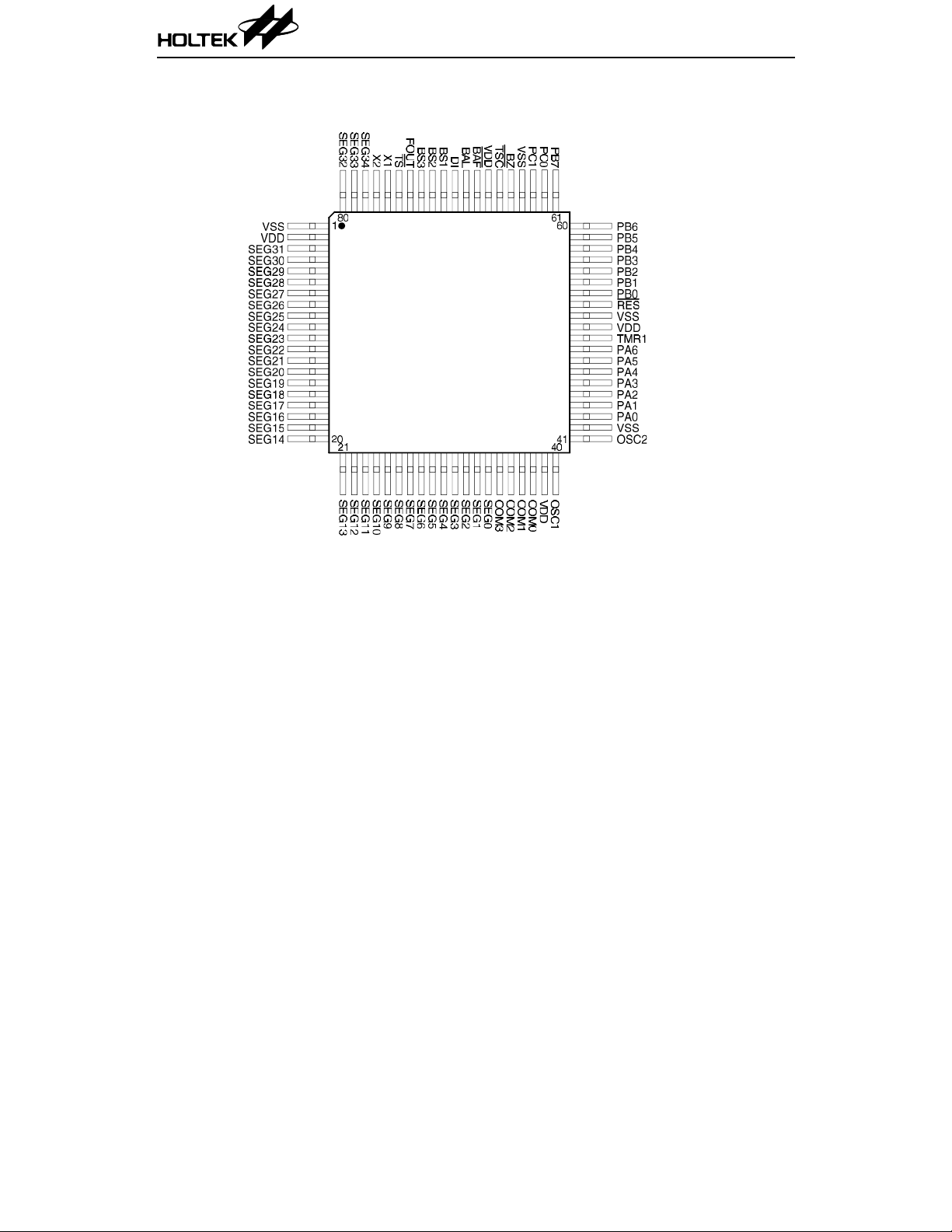
Pin Assignment
HT9480
2 23th Feb ’98
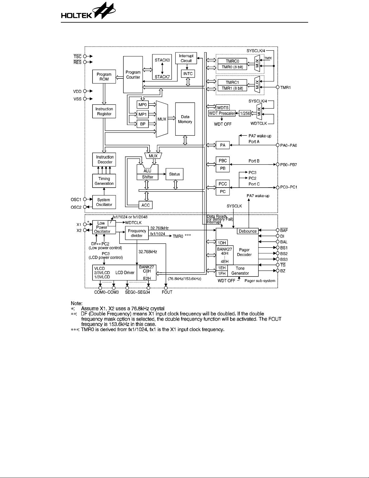
Block Diagram
HT9480
3 23th Feb ’98
HT9480
Pin Description
Pin No Pin Name I/O Function
43~49 PA0~PA6 I
54~61 PB0~PB7 I/O
62~63 PC0~PC1 I/O
1, 42,
52, 64
76
77
40
41
53
68
50 TMR1 I Schmitt trigger input for timer/event counter
2, 39, 51
67
65 BZ O
3~34
78~80
35~38 COM3~COM0 O Outputs for LCD panel common connections
66
75
69 BAL I
70 DI I
71 BS1 O Pager receiver power control enable output, CMOS output
72 BS2 O RF dc level adjustment pin, CMOS output
73 BS3 O PLL control pin, CMOS output
74 FOUT O
VSS Negative power supply (GND)
X1
X2
OSC1
OSC2
RES I Schmitt trigger reset input, active low
BAF I Battery fail interrupt with debounce circuit input
VDD Positive power supply
SEG31~SEG0
SEG34~SEG32
TSC I
TS I Decoder test mode input pin, active low with a pull-high resistor
7-bit input ports, with pull-high resistors
Each bit can be configured as a wake-up input by mask option.
Bidirectional 8-bit input/output ports, pull-high mask option
The output structures, whether tri-state or CMOS, are
determined by software instructions.
Bidirectional 2-bit input/output ports, pull-high mask option
The output structures, whether tri-state or CMOS, are
determined by software instructions.
IOX1 and X2 are connected to an external crystal to form an
internal low power oscillator clock.
OSC1 and OSC2 are connected to an RC network or a crystal
I
(determined by mask option) to form the system clock oscillator.
O
For RC operation , OSC2 is the output terminal of the system
clock.
Buzzer non-inverting BZ output
The BZ pin outputs “high” at buzzer off (by setting the value 00H
of 1DH)
O LCD driver outputs for LCD panel segments
µC test mode input pin, active low with pull-high resistor
Battery low indication input, active high without pull-high
resistor
POCSAG cod e input serial da ta (inverting o r non-inve rting as
determined by SPF32). CMOS input without pull-high resistor
Frequency reference output pin
The FOUT output pin produces a 76.8kHz/153.6kHz signal with
a 1/2 duty cycle reference frequency if a 76.8kHz crystal is used.
4 23th Feb ’98
HT9480
Absolute Maximum Ratings*
Supply Voltage.......... ................ ....–0.3V to 5.5V
Input Voltage..................V
–0.3V to VDD+0.3V
SS
*Note: Stresses above those listed under “Absolute Maximum Ratings” may cause permanent
damage to the device. The se are stress ratings on ly. Functional opera tion of this device at
these or any other conditions above those indicated in the operational sections of this
specification is not implied and exposure to absolute maximum rating conditions for extended
periods may affect device reliability.
Storage Temperature.................–50
Operating Temperature...............–25
°C to 125°C
°C to 85°C
D.C. Characteristics
Symbol Parameter
V
DD
I
DD
I
STB1
I
STB2
V
IL
V
IH
V
IL1
V
IH1
V
IL2
V
IH2
I
OL
I
OH
I
OL
I
OH
I
OL
I
OH
Operating Voltage — 3V application 2.2 3.0 3.5 V
Operating Current 3V
Standby Current 1 3V
Standby Current 2 3V
Input Low Voltage for
Input Port and I/O Port
Input High Voltage for
Input Port and I/O Port
Input Low Voltage
(
RES,TMR1,BAL)
Input High Voltage
(
RES,TMR1,BAL)
Input Low Voltage (BAF) 3V — 0 — 0.9 V
Input High Voltage (BAF) 3V — 1.3 — 3 V
I/O Port Sink Current 3V VOL=0.3V 1.7 3.4 — mA
I/O Port Source Current 3V VOH=2.7V –1 –1.9 — mA
Segment 0-34 Output
Sink Current
Segment 0-34 Output
Source Current
BZ, Sink Current 3V VOL=0.3V 1 2.5 — mA
BZ, Source Current 3V VOH=2.7V –1 –2 — mA
(Ta=25°C)
Test Conditions
V
DD
Conditions
No load,
fsys=153.6kHz
No load, System
HALT (Watchdog ON)
No load, System
HALT (Watchdog OFF)
Min. Typ. Max. Unit
—300—
—200—
—— 1
3V — 0 — 1 V
3V — 2.2 — 3 V
3V — 0 — 1 V
3V — 2.2 — 3 V
3V V
3V V
=0.3V 20 44 —
OL
=2.7V –20 –38 —
OH
µA
µA
µA
µA
µA
5 23th Feb ’98
HT9480
Symbol Parameter
I
OL
I
OH
I
OL
I
OH
R
PH
PC0~PC1 Sink C urrent 3V VOL=0.3V 1.7 3.4 — mA
PC0~PC1 Source Current
if Pull-High Mask Option
BS1, BS2, BS3, FOUT Sink
Current
BS1, BS2, BS3, FOUT
Source Current
Pull-High I/O Port
Resistance
A.C. Characteristics
Symbol Parameter
f
SYS1
f
SYS2
f
SUBSYS
f
TIMER
t
RES
t
INT
System Clock (RC OSC) 3V — 76.8 256 1000 kHz
System Clock (Crystal OSC) 3V — 76.8 256 1000 kHz
Pager Subsystem Clock
(Crystal OSC)
Timer I/P Frequency (TMR1) 3V — 0 — 1000 kHz
External Reset Low Pulse Width — — 1 — —
Interrupt Pulse Width — — 1 — —
Test Conditions
V
DD
3V V
3V V
3V V
OH
=0.3V 350 — —
OL
OH
Conditions
=2.7V –1 –1.9 — mA
=2.7V –0.9 — — mA
Min. Typ. Max. Unit
3V — 100 200 500
Test Conditions
V
Conditions
DD
Min. Typ. Max. Unit
3V — 32.768 76.8 153.6 kHz
µA
Ω
k
(Ta=25°C)
µs
µs
* Note: t
SYS
=1/f
SYS
6 23th Feb ’98
System Architecture
HT9480
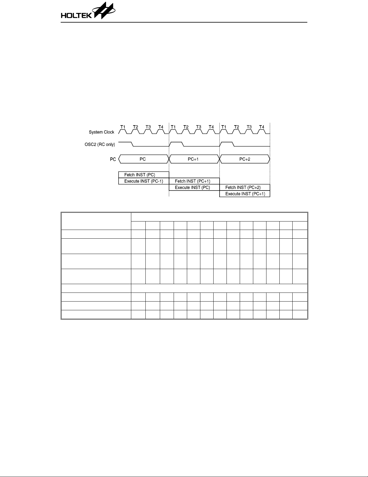
Execution flow
The HT9480 system clock can be derived from
either a crystal or an RC o scillator. It is internally divided into four non-overlapping clocks
denoted by P1, P2, P3, and P4. Each instruction
cycle consists of T1 to T4.
Instruction fetching and execution are pipelined in such a way that a fetch takes an instruction cycle while decoding and execution
take the next instru ction cycle. The p ipelining
Execution flow
Mode
Initial reset 0000000000000
Data ready interrupt and
battery fail interrupt
Programmable timer
interrupt
Timer/event Counter
interrupt
Skip PC+2
Loading PCL *12 *11 *10 *9 *8 @7 @6 @5 @4 @3 @2 @1 @0
Jump, call branch #12#11#10#9#8#7#6#5#4#3#2#1#0
Return from subroutine S12 S11 S10 S9 S8 S7 S6 S5 S4 S3 S2 S1 S0
*12 *11 *10 *9 *8 *7 *6 *5 *4 *3 *2 *1 *0
0 000000000100
0 000000001000
0 000000001100
scheme causes each instruction to effectively
execute within a cycle. If an instruction changes
the content of the progra m counter two cycles
are required to complete the instruction.
Program counter – P C
The program cou nter (PC) is 13-bit wide and
controls the program ROM instruction sequence executi on. The contents of th e PC can
specify a of maximum 8192 addresses.
Program Counter
Notes:
*12~*0: Program counter bits
#12~#0: Instruction code bits
Program counter
S12~S0: Stack register bits
@7~@0: PCL bits
7 23th Feb ’98
The PC value is incremented by one after a
program memory word is accessed in order to
fetch an instruction code. The PC then points to
a memory word with the next instruction code.
The PC loads the address corresponding to each
instruction and then manipulates program
transfer while executing a jump instruction,
conditional skip execution, loading a PCL, a
register, a subroutine call, an i nitial reset, an
internal interrupt, an external interrupt, or returning from a subroutine.
The conditional skip is activated by instructions. Once the condi tion is satisfied, the next
instruction, fetched duri ng the current instruction execution, is discarded, and a dummy cycle
is replaced to get a proper instruction. Oth erwise it proceeds with the following instruction.
The low byte of the PC (PCL) is a readable and
writable register (06H). Moving data into the
PCL performs a sho rt ju mp. Th e des tin ation i s
within 256 locations.
If a control transfer takes pla ce, an additional
dummy cycle is required.
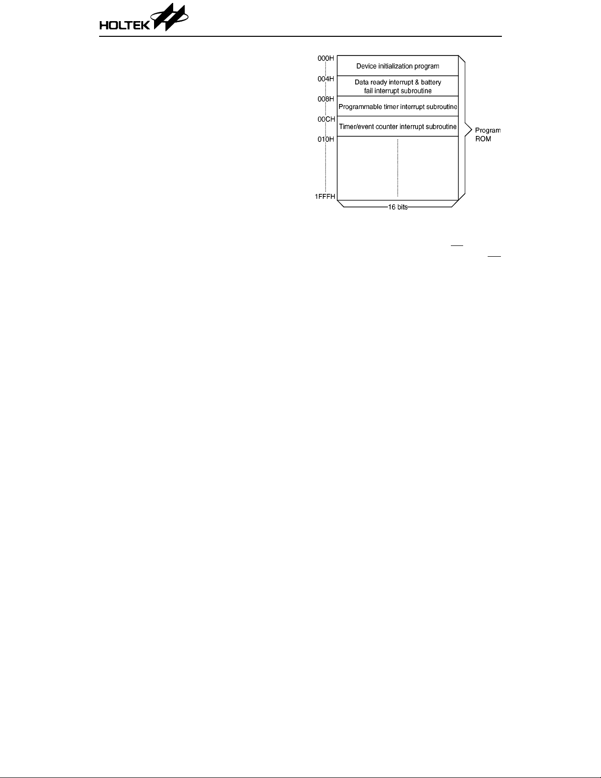
Program memory – ROM
The program memory (ROM) is used to store
the program instructions that are to be executed. It consists of data, table(s), and interrupt
entries, and is organized into 8192
×16 bits,
which are addressed by the PC and table pointer.
Certain location s in the ROM are reserved for
specific usage:
•
Location 0000H
Location 0000H is reserved for program in-
itialization. The progra m always begins execution at this lo cation each time the chip is
reset.
•
Location 0004H
Location 0004H is reserved for the data ready
interrupt and battery fail interrupt service
programs. If an interrupt results from a pager
decoder inte rrupt request or from a battery
fail interrupt request, and the interrupt is
enabled, and the stack is not full, the program
begins exe cution at location 0004 H. The occurrence of a data ready interrupt or a battery
HT9480
Program memory
fail interrupt is detected by checking the battery fail interrupt bit (1EH-bit 4,
the data ready inte rrupt bit (1EH-bit 7,
flag). The interrupt shou ld be carefu lly processed if both interrupt bits are active.
•
Location 0008H
Location 0008H is reserved fo r the program-
mable timer interru pt service program. If a n
interrupt results from a programmable timer
interrupt request (its source is from 256Hz
divided by N, where the value of N ranges
from 1 to 256.), and the in terrupt is enab led,
and the stack is no t full, the program begins
execution at location 0008H.
•
Location 000CH
Location 000CH is reserved for the timer/event
counter interrupt service program. If a timer
interrupt results from a timer/event counter
overflow, and the interrupt is enabled, and the
stack is not full, the program begins execution
at location 000CH.
•
Look-up tables XX00H~XXFFH
The ROM is composed of 32 groups (each
group contains 256 con tinuous words) whi ch
can be used as look–up tables. The instructions “TABRDC [m]” (the current table) and
“TABRDL [m]” (the last table) transfer the
contents of the low-order byte to the specified
data memory , and the contents of the high-order byte to TBLH (Table High-order Byte Reg-
BF flag) and
DR
8 23th Feb ’98

HT9480
ister) (08H). Only the destination of the loworder byte in the table is well-defined, the
other bits of the table word are all transferred
to the low portion of TBLH. TBLH is read only
while the table pointer (TBLP) is a readable/writable register (0 7H) used to indicate
the table location. Befo re accessing the tab le,
the location should be placed in TBLP. All of
the table related instructions require 2 cycles
to complete the operation. This feature is efficient only for the movement of the blocks,
which may functio n as look-u p tables o r as a
normal program memory depending upon the
requirements.
Stack register – STACK
The stack register is a special memory port used
to save the contents of the PC. It is divided into
8 levels. The stack register is neither part of the
data nor part of the program, and is neither
readable nor writable. The activated level of the
stack register is indexe d by the stack pointer
(SP), and is neither readable nor writable. At
the commen cement of a subroutine ca ll or an
interrupt acknowledge, the contents of the PC is
pushed onto the stack. At the end of the subroutine or the interrupt routine , as signaled by a
return instruction (RET or RETI), the content s
of the PC is restored to its previo us value from
the stack. After a chip reset, the SP will point to
the top of the stack.
If the stack is fu ll and a non-m aske d interrupt
occurs, the interrupt request flag is recorded
but acknowledging is inhibited unti l the value
of the SP is decremented (by RET or RETI),
allowing that interrupt to b e serviced. As this
feature can prevent a stack overflow, the use of
the structure becomes much easier. In a similar
case, if the stack is full, and a “CALL” is subsequently executed, a stack overflow occurs and
the first entry is lost (only the most recent eight
return addresses are stored).
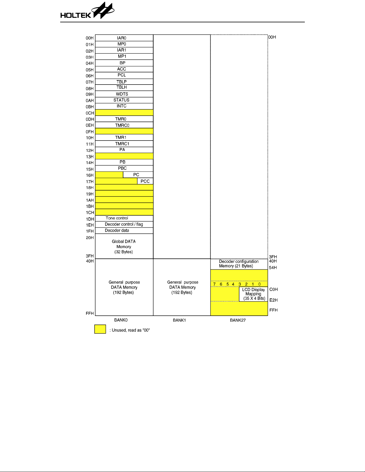
Data memory – RAM
The data memory (RAM) is designed in three
banks, i.e., bank 0, bank 1, and bank 27, and
comprised of four functional groups, namely
special function regis ters (of 22
1
×2 bit in bank0), data memory (of 416×8 bits;
224
×8 in bank 0; 19 2×8 in bank 1), LCD dis play
mapping memory (of 35
configuration RAM mapping m emory (of 21
bits). Most of the these groups are readable/writable but some are read only.
Of the four functional grou ps, the special function registers of ba nk 0 consist of an indirect
addressing registers (IAR0;00H, IAR1;02H),
memory pointer registers (MP0;01H,
MP1;03H), a memory bank pointer register
(BP;04H), an accumulator (ACC;05H), a program counter low byte register (PCL;06H), a
table pointer (TBLP;07H), a table high-order
part register (TBLH;08H), a watchdog timer
option setting register (WDTS;09H), a status
register (STATUS;0AH), an interrupt control
register (INTC;0BH), a programmable timer
counter (TMR0;0DH), a programmable timer
counter control register (TMRC0;0EH), a
timer/event counter (TMR1;10H), a timer/event
counter control register (TMRC1;11H), an input
port, two I/O ports (PA;12H, PB;14H, PC;16H),
two I/O control register (PBC;15H, PCC;17H), a
tone control register (1DH), a pager control register (1EH), and a page r data register (1FH).
The special fu nction regi sters are located from
00H to 1FH where as the 32 global data regi s-
×8 bits; 1×4 bit;
×4 bits), and decoder
×8
Instruction(s)
Table Location
*12*11*10*9*8*7*6*5*4*3*2*1*0
TABRDC [m] P12 P11 P10 P9 P8 @7 @6 @5 @4 @3 @2 @1 @0
TABRDL [m] 11111@7@6@5@4@3@2@1@0
Notes:
*12~*0: Table location bits
@7~@0: Table pointer bits
P12~P8: Current p rogram counter bits
9 23th Feb ’98
HT9480
RAM mapping
10 23th Feb ’98

HT9480
ters are from 20H to 3FH, where each bank
points to the same location. The other spaces ,
namely 0CH, 0FH, 13H, the high n ibble of 16H,
17H, and 18H~1CH, are all reserved for futu re
expansion usage; reading these locations will
get an “00H” value.
On the other hand, the general purpose data
memory, divi ded into thr ee banks (bank 0, bank
1, and bank 27), is used for data, control information, and LCD display control under instruction commands. The banks in the RAM are all
addressed from 40H to FFH, and are selected by
setting the value (“00H”: bank 0; “01H” : bank 1;
“1BH”: bank 27) of the bank pointer (BP;04H).
The bank27 memory is used for LCD display
mapping and the decoder configuration RAM
mapping. The spaces from 4FH to BFH and
from E3H to FFH, and the high nibble part from
C0H to E2H in bank 27 are all reserved for
future expansion usage; reading these locations
will derive “00H”.
The special regis ters, glob al data registe rs and
general data memory can directly perform
arithmetic, logic, increment, decrement, and rotate operations. Each bit in the RAM can be set
and reset by “SET [m].i” and “CLR [m].i”, and
can also be indirectly accessible through the
memory pointer registers (MP0;01H, MP1;03H).
Of the speci al a d dres se s, 1 DH an d 1F H ca nn ot
directly do all these operations, because they
are not read and write accessible addresses.
1DH is a write-only a ddress, 1FH a read-only
address, but these two a ddresses nam ely, 1DH
and 1FH can only perfo rm operatio ns by using
the “MOV” instruction.
Indirect addressing register
IARx (IAR0;00H, IAR1;02H) are indirect address registers that are not physically implemented. Any re ad/write operation of the IARx
accesses the data memory pointed to by MPx
(MP0;01H, MP1;03H). Reading the indirect addressing register itself will indirectly derive
00H, while writing the indirect addressing register indirectly will lead to no operations. (IAR0,
MP0) is indirectly addressable in bank 0, but
(IAR1, MP1) is available for all banks.
Accumulator – ACC
The accumulator (ACC) relates to the ALU operations. It is also mapped to location 05H of the data
memory and is capable of carrying out immediate
data operations. Data movement between these
two data memories has to pass t hrough t he ACC.
Arithmetic and logic unit – ALU
This circuit performs 8 -bit ari thm etic and logic
operations, and provides the following functions:
•
Arithmetic operation (ADD, ADC, SUB, SBC, DAA)
•
Logic operation (AND, OR, XOR, CPL)
•
Rotation (RL, RR, RLC, RRC)
•
Increment and decrement (INC, DEC)
•
Branch decision (SZ, SNZ, SIZ, SDZ, etc.)
The ALU not only saves the results of data
operation, but also changes th e contents of the
status register.
Status register – STATUS
The status register (0AH) is 8-bit wide. It contains
a zero flag (Z), a carry flag (C), an auxiliary carry
flag (AC), an over flow flag (O V), a powerdown flag
(PD), and a WDT time-out flag (TO). The status
register not only records the status information,
but also controls the operation sequence.
The status re gister, like most other regis ters,
can be altered by instructions except for the TO
and PD flags. Any d ata written into the status
register will not change TO or PD. It should be
noted that ope ration s re la ted to the statu s register may derive different results from those
intended. For exa mp l e, cleari ng th e statu s register CLR [0AH] has no effect on the TO and PD
flags, and the value of the zero flag is also “1”,
i.e., UU0100 is the data in the register, where
the value of U is an unchanged value.
The Z, OV, AC, and C flags generally reflect the
status of the latest operations.
On entering an interrupt sequence or executing
a subroutine call, the status register will not be
automatically pushed onto the stack. If the contents of the status is i mpo rtan t , and if the su broutine may corrupt the status register, the
programmer should take preca utions to sa ve it
properly.
11 23th Feb ’98

Labels Bits Function
C is set if the operation results in a carry out in additi on or if a borrow does not
C0
AC
Z2
OV
PD 4 PD is cleared during power up, and set by a “HALT” instruction.
TO 5
−
−
take place in s ubtraction; otherwis e C is cleared. C is also affected b y a rotate
through carry instructions.
AC is set if the operation results in a carry out of the low nibbles in addition or if
1
a borrow from the high nibble into the low nibble does not take place in
subtraction; otherwise AC is cleared.
Z is set if the resul t of an arith metic or a l ogic operati on is zero; o therwise Z is
cleared.
OV is set if the operation results in a carry into the high-order bit but not a carry
3
out of the high-order bit, or vice versa; otherwise OV is cleared.
TO is cleared during power up o r by a “CLR WDT” instruction and a “HALT”
instruction. TO is set by a current timer time-out.
6 Undefined, read as “0”
7 Undefined, read as “0”
STATUS register
HT9480
Interrupts
The HT9480 pr ovides an i nternal programm able timer inte rrupt, an internal d ata ready interrupt, timer/event counter interrupt, and a
battery fail interrupt. The inte rnal data ready
interrupt and the battery fail interrupt employ
the same jump location (04H). The interrupt
control register (INTC;0BH) contains interrupt
control bits to set no t only the enab le/disable
status but also the interrupt request flags.
Once an interrupt subro utine is serviced, the
other interrupts will all be blocked (by clearing
the EMI bit). This scheme may prevent any
further interrupt ne sting. Other interrupt requests may occur during this interval, but only
the interrupt re quest fla g is record ed. If a certain interrupt requires servicing within the
service routine, the EMI bit and the corresponding bit of the INTC register may be set to permit
interrupt nesting. W hen the stack is full, the
interrupt request will not be acknowledged
even if the related interrupt is enable d, until
the SP is decreme nted. If imme diate service i s
desired, the stack should be prevented from
becoming full.
All of these interrupts can support the wake-up
function. As an interrup t is serviced , a contro l
transfer occurs by pushing the contents of the
PC onto the stack, followed by a branch to a
subroutine at the specifi ed loca tion in the program memory. Only the contents of the PC is
pushed onto the stack. If the contents of the
register or of the status re gister (STATUS) is
altered by the interrupt service program which
corrupts the desire d control sequence, the contents should be saved in advance.
The data ready interrupt and battery fail interrupt share the same subroutine call location
04H. Checking the battery fail interrupt bit
(
BF;bit 4 of 1EH) and th e da ta re ady inte rrup t
bit (
DR; bit 7 of 1EH) can determine which kind
of interrupt has occurred. The value of 1EH-bit
7
DR is cleared “0” by the decoder data ready
interrupt signal, and is set to “1” when the
sets this bit high. Both interrupt bits are active
low.
The data ready inte rrupt is generated by the
pager decoder after a valid call is received, and
is initialized by setting the data ready interrupt
request flag (EIF; b it 4 of INTC) and th e data
µC
12 23th Feb ’98

HT9480
ready interrupt bit (DR; bit 7 of 1EH). Once the
data ready interru pt is triggered, the stack is
not full, and the EMI bit is set, a subroutine call
to location 04H will occur. The related interrupt
request flag (EIF) will, however, be reset, and
the EMI bit cleared to disable further interrupts. This interrup t sh ou ld be pro ces se d carefully if the battery fail interrupt is activated as
well.
The battery fail interrupt, on the other hand, is
triggered by a high to low transition on
When the battery fail interrupt is enabled, the
stack is not fu ll, an d th e interru pt requ es t fl ag
(EIF; bit 4 of INTC) is set, a subroutine call to
location 04H wil l occur. The related interrupt
request flag (EIF) will also be reset, and the
EMI bit be cleared to disable other interrupts.
The programmable timer interrupt is automatically triggered at a rate of 256Hz/N (where the
value of N ran ges from 1 to 256), and th en the
interrupt req uest flag (T0F; bit 5 of INTC) is
set. When the timer i nterrupt is enabled, the
stack is not full, and the programmable tim er
interrupt is activated, a subroutine call to location 08H will occur. Then, the related interrupt
BAF.
request flag (T0F) will be reset, and the EMI bit
cleared to disable other interrupts.
The timer/event counter interrupt is initialized
by setting the timer/event counter interrupt request flag (T1F; bit 6 of INTC), which is normally caused by a timer overflow. When the
interrupt is ena bled, the stack is not ful l, and
the T1F bit is set , a subroutine call to location
0CH will occur. The related interrupt request
flag (T1F) will be reset, and the EMI bit cleared
to disable further interrupts.
During the execution of an interrupt subroutine, other interrup t acknowledgments are all
held until the “RETI” instruction is executed, or
the EMI bit and the related interrupt control bit
are both set to 1 (if the stack is not full). To
return from the in terrupt subroutine, a “RET”
or “RETI” instruction may be invoked. RETI
will set the EMI bit to enable an interrupt service,
but RET will not.
The interrupts are serviced between the rising
edges of the two adja cent T2 clocks. In cas e of
simultaneous requests, the following table
shows the priority that is applied. These can be
masked by resetting the EMI bit.
Register Bit No. Label Function
Controls the master (global) interrupt
(1=enabled; 0=disabled)
Controls the data ready and battery fail interrupts
(1=enabled; 0=disabled)
Controls the programmable timer interrupt
(1=enabled; 0=disabled)
Controls the timer/event counter interrupt
(1=enabled, 0=disabled)
Internal data ready and battery fail interrupt request flag
(1=active; 0=inactive)
Internal programmable timer interrupt request flag
(1=active; 0=inactive)
Timer/event counter request flag
(1=active; 0=inactive)
INTC register
13 23th Feb ’98
INTC
(0BH)
0EMI
1 EEI
2ET0I
3ET1I
4EIF
5T0F
6T1F
7 -- Unused bit, read as “0”
NO. Interrupt Source Priority Vector
Data ready
interrupt and
a
battery fail
interrupt
Programmable
c
timer interrupt
Timer/event
d
counter overflow
The programmable timer interrupt request flag
(T0F), timer/event counter interrupt request
flag (T1F), data ready interrupt and battery fail
interrupt request flag (EIF), enable timer/event
counter bit (ET1I), enable data ready interrupt
bit (EEI), and ena ble programmable timer interrupt bit (ET0 I) make up the regi ster INTC
which is located at 0BH in the data memory.
The EEI, ET0I, ET1I, and EMI bits are all use d
to control the enable/disable status of the interrupts, preventing the requested interru pt from
being serviced. Once the interrupt request flags
(T0F, T1F, and EIF) are set, t hey wil l r emain in
the INTC register until the interrupts are serviced or cleared by a software instruction.
A “CALL subroutine ” in the interrupt subroutine should be u sed. This is beca use interrup ts
often occur in an unpredictable manner or need
to be immediately serviced in some applications. During this time, if only one stack is left,
and enabling the inte rrupt is not well controlled, the operation of a “CALL subroutine” in the
interrupt service routine is quite likely to upset
the original control sequence.
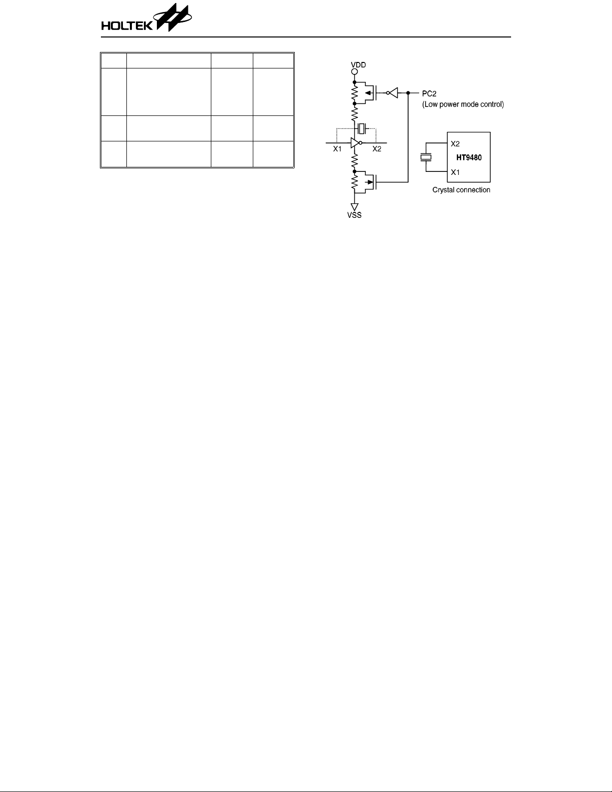
Oscillat or co nf iguration
The system core and the pager subsystem of the
HT9480 are clocked by different oscillators. The
system oscillato r can be either a crystal or an
RC type. The su bsystem low power osc illator , on
the other hand, is a crystal type which is designed with the power on start-up function to
reduce the stabili zation time of the oscillator.
This start-up function is enabled by PC2 which
is initially set high at power on reset, and
should be clea red so a s to en ab le th e low - power
oscillator functi on . T he oscil la tor co nfigura tio n
is running in the low power mode.
104H
208H
30CH
HT9480
Low power oscillator
The system oscillator can be configured as
either an RC or crystal type of oscillator , determined by mask option. No matte r what kind of
oscillator type is selected, the signal provides a
system clock. The system clock may also be
externally connected. The HALT mode stops
the system osci llator and igno res external signals to conserve power.
If the system oscillator is an RC type oscillator,
an external resistor between OSC1 and OSC2 is
required. The system clock is available on
OSC2, which can be used to syn chro nize e xternal logic. An RC oscillator provides the most
cost-effective solution. The frequency of oscillation may vary with power , temperature, and the
chip itself due to process variations. The RC
oscillator is, there fore, not suitable for timing
sensitive opera tions wh ere an accurate oscill ator frequency is desired.
On the other hand, if a crystal type oscillator is
used, a crystal across OSC1 and OSC2 is required to provide the feed back and phase shift
for oscillation, and no other external components are required. A ceramic resonator can
replace the crystal connected between OSC1
and OSC2 to derive a frequency reference. In
this case, two e xtern al ca paci tors at OSC 1 a nd
OSC2 are required.
14 23th Feb ’98
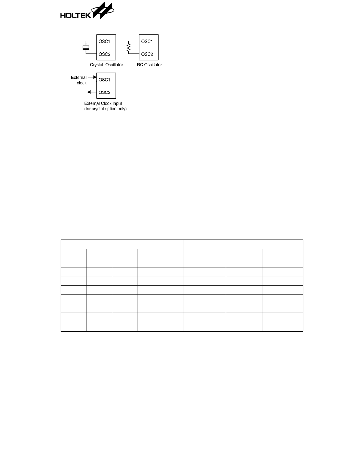
System clock oscillator
An external clock can also be applied to OSC1 .
In this application, the mask option for the
crystal type osci llator should be selected , and
OSC2 kept open.
The low power crystal oscillator is designed for
the pager subsystem and is used to clock the
frequency divider, pager decoder, and LCD
driver. When the system enters the powerdown
mode the crystal oscillator for the pager subsystem keeps running.
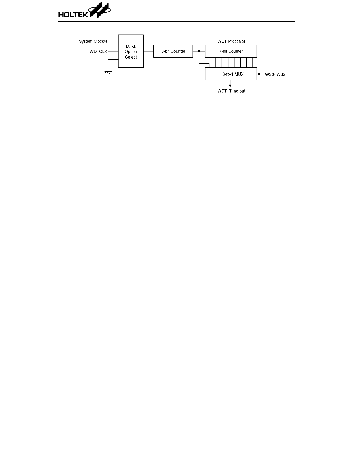
Watchdog timer – WDT
The clock source of the watchdog timer (WDT )
is implemented by a subsystem clock
(WDTCLK from the pager subsystem which remains running during a system halt) or by an
HT9480
instruction clock (the syste m clock divided by
4), that is deci ded by ma sk op ti on . Th e v a lu e of
WDTCLK can be set as 153.6kHz/1024 (or 2048),
76.8kHz/1024 (or 2048), or 32.768k Hz/1024 (or
2048), depending upon the different crystal
type. The WDT is the program designed to
avoid software m alfunctions or sequence from
jumping to an unknown location with unpredictable results. It can be disabled by mask
option. If the WDT is disabled, all the executions related to the WDT lead to no operations.
If the subsystem clock is selected, it is first
divided by 256 (8 stages) to get the nominal
time-out period. Longer tim e-outs can be realized by invoking the WDT prescaler. Writing
data to WS2, WS1, and WS0 (b its 2,1,0 of the
WDTS) can yie ld different time -out periods. If
the values of WS2, WS1, and WS0 are all equal
to 1, the division ratio is up to 1:128.
On the other hand, if th e instruction clock is
applied, the WDT operates in the same manner
as the case when the subsystem clock is chosen,
except that i n the HALT state the W DT stops
counting and lose its protection purpose. In this
situation, the WDT logic can be restarted by
external logic. The high nibble a nd bit 3 of the
WDTS is reserved for user defined flags, which
can be used to indicate some specified status.
The overflow of the WDT under normal ope ration not only initializes the “chip reset”, but sets
the status bit “TO”. An overflow in the HALT
Division Ratio Option Crystal Type and Time-Out Period
WS2 WS1 WS0 Division Ratio 153.6kHz 76.8kHz 32.768kHz
0 0 0 1:1 13.3ms 26.7ms 6 2.5ms
0 0 1 1:2 26.7ms 53.3ms 125ms
0 1 0 1:4 53.3ms 106.7ms 250ms
0 1 1 1:8 106.7ms 213.3m s 5 00ms
1 0 0 1:16 213.3ms 426.7ms 1000ms
1 0 1 1:32 426.7ms 853.3ms 2000ms
1 1 0 1:64 853.3ms 1706.7ms 4000ms
1 1 1 1:128 1706.7ms 3413.3ms 8000ms
WDTs register
15 23th Feb ’98
Watchdog timer
HT9480
mode initializes a “warm reset” only when the
PC and SP are reset to zero. To clear the contents of the WDT (including the WDT prescaler), there are three methods to be ado pted
namely, external reset (a low level to
software instruction(s) , and a “HALT” instruction. There are two typ es of software instructions, “CLR WDT” and “CLR WDT1”/“CLR
WDT2”. But only one of these two types of instructions can be active at a time depending on
the mask op tion
option”. If the “CLR WDT” is selected (i.e.,
CLRWDT times equal one), any execution of the
“CLR WDT” instruction clears the WDT. In the
case that “CLR WDT1” and “CLR WDT2” are
chosen (i.e ., CLRWDR times equal two), th ese
two instructions should be executed to clear the
WDT; otherwise, the WDT may reset the chip
due to a time-out.
Powerdown opera tion – HALT
The HALT mode is initialized by the “HALT”
instruction and results in the following.
The system tu rns o ff. The low power os cilla tor,
tone generator, LCD driver, pager decoder, and
WDT oscillator all keep running (if the WDT
oscillator is selected).
The contents of the on–chip RAM and of the
registers remain unchanged.
The WDT and th e WDT prescaler are cleared
and counted again (if the WDT clock is from the
WDT oscil lator).
All the I/O ports remain in their original status.
The PD flag is set but the TO flag is cleared.
The system can quit the HALT mode by an
− “CLR WDT tim es selection
RES),
external reset, an interrupt, an external falling
edge signal on port A, or a WDT overflow. An
external reset leads to device initialization and
the WDT overflow performs a “warm reset”.
After the TO an d PD flags are examined, the
reason for the chip reset is determined. The PD
flag that is cleared on power-up is set afte r the
“HALT” instruction is execute d. The TO fla g is
set when the WDT time-out occurs, which
causes a wake-up that resets only the PC and
SP, and leaves the others in their original status.
The port A wake-up and interrupt me thods can
be considered as a continuation of normal execution. Every bit in port A can be independently
selected to wake up the device by mask option .
Awakening from an I/O port stimulation, the
program resumes execution of the next instruction. However, if the program awakens from an
interrupt, two sequences may occur. The program will resume execution at the next instruction if the rela ted interrup t(s) is (are) di sabled
or the interrupt(s) is (are) enabled but the stack
is full. A regular interrupt response, on the
other hand, may tak e place if the interrupt is
enabled and the stack is not full.
If the wake-up event(s) occurs and the wake-up
results from an interrupt acknowledge, the actual
interrupt subroutine execution is delayed by one
or more cycles. On the oth er han d, if the wak eup brings about the following instruction execution, the actual interrupt subroutine is executed
immediately after the dummy period is completed.
To minimize power consumption, the I/O pins
should all be carefully managed before entering
the HALT status.
16 23th Feb ’98
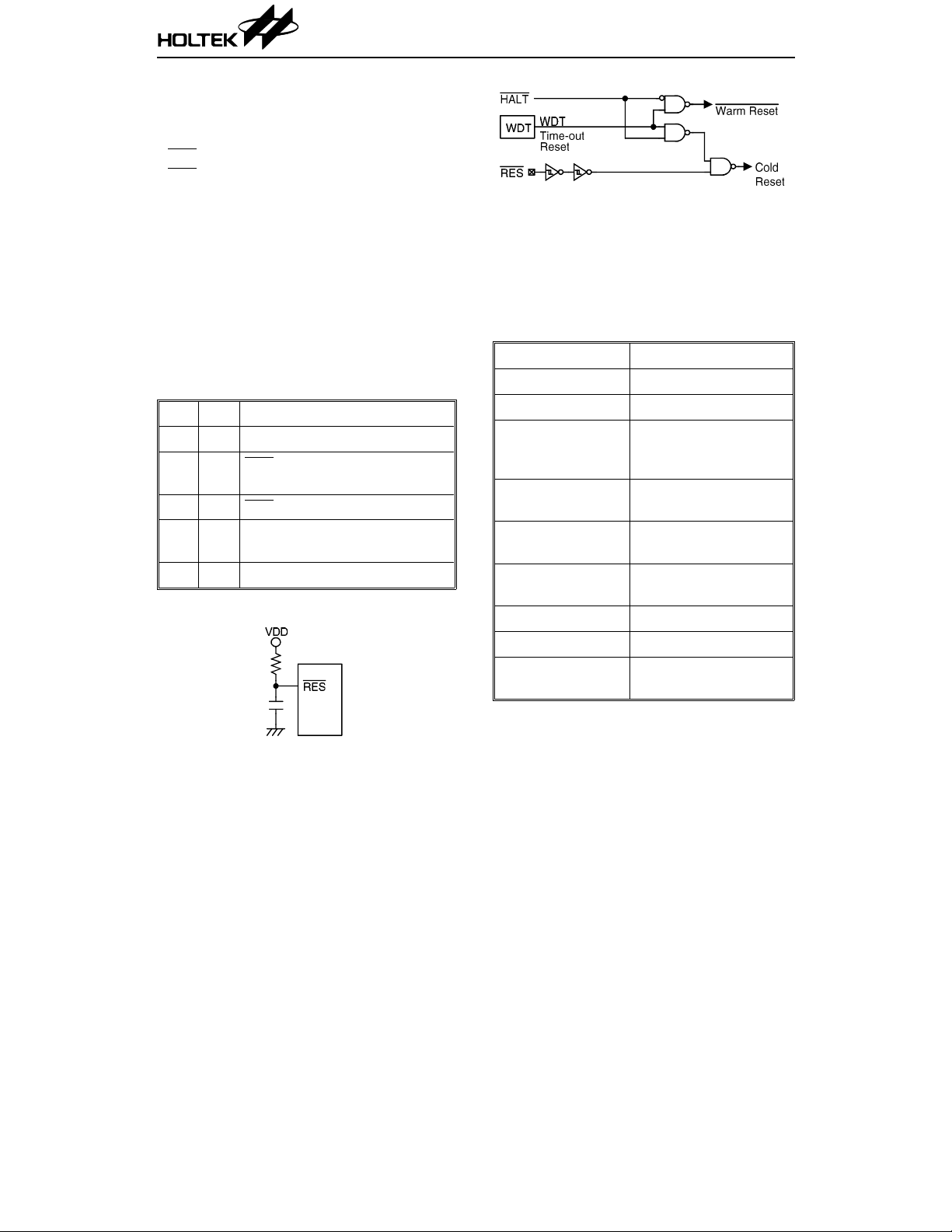
Reset
There are five ways in which a reset can occur:
•
Power on reset (POR)
•
RES reset during normal operation
•
RES reset during HALT
•
WDT time-out reset during norma l oper ati on
•
WDT time-out reset during HALT
The WDT time-out during HALT is different
from other chip reset conditions, since it can
perform a “warm reset” that just resets the PC
and SP, leaving the other ci rcuits to ke ep their
state. Some registers remain unchanged during
other reset conditi ons. Most registers are reset
to the “initial condition ” when the reset conditions are met. By examining the PD and TO
flags, the program can distinguish between different “chip resets”.
TO PD RESET Conditions
0 0 Power on reset
uu
01
1u
RES reset during normal
operation
RES wake-up HALT
WDT time-out during normal
operation
1 1 WDT wake-up HAL T
Note:“u” means “unchanged”
HT9480
Reset configuration
If crystal mask option is selected , the
can be fed by X1, X2 decoder input clock (See
Application Circuit 2).
The functional un its ch ip res et sta tus is shown
in the following table.
PC 0000H
Interrupt Disabled
Prescaler Cleared
Cleared. After master
WDT
reset, WDT starts
counting.
Programmable
timer Counter
Timer/event
Counter
Programmable
Tone Generator
Off
Off
Off
Pager Decoder Off
Input/output Ports input mode
SP
Points to the top of the
stack
µC clock
Reset circuit
17 23th Feb ’98

HT9480
Programmable timer counter and
timer/event counter
The programmable timer co unter (TMR0) and
timer/event counter (TMR1) are constructed using the same structure. Both counters contain
an 8–bit programmable count-up counter,
whose clocks may come from an external
source or from the system clock divided by 4.
If the internal instruction clock is selected, only
one reference time-base is pro vided . The external clock input allows the user to count external
events, measure time intervals or pulse widths,
or generate an accurate time base. The clock of
the programmable timer counter should com e
from the external clock of the 75Hz for Real
Time Clock (RTC) if a 76.8kHz crystal is used.
There are two sets of regis ters related to the
programmable timer counter and to the
timer/event counter namely, TMR0 (0DH) and
TMRC0 (0EH) and TMR1 (10H) and TMRC1
(11H). There are also two physical registers
mapped to the TMR0 and TMR1 locations:
Writing to TMR0 and TMR1 puts the starting
value in the programmable tim er counter and
in the timer/event counter preload registers,
while reading them gets the contents of the two
counters. TMRC0 and TMRC1 are co ntrol registers used to define some timer options.
The TM0 and TM1 bits define the operation
mode. The event count mode is used to count
external events, which means that the clock
source may come from either a 256Hz generator
(for TMR0) or an external pin (for TMR1) . The
timer mode fu nctions as a normal timer, with
the clock source coming from the instruction
clock or from the outputs of the TMR1 prescaler
(TMR0 cannot be us ed i n th is mo de). The pulse
width measurement mode can be used to count
the high or low level duration of the exte rnal
signal TMR1, TMR0 is also disabled in this
mode. The counting is based on the system
clock.
In the event count or timer mode, once the
programmable timer counter or timer/event
counter starts counti ng, it will count from th e
current contents in the counter to FFH. Once an
overflow occurs, the counter is reloaded from its
counter preload register a nd generates an interrupt request flag (T0F; bit 5 of INTC and
T1F; bit 6 of INTC for programmable timer
counter and timer/event counter, respectively).
On the other hand, in the pulse width measurement mode with t he TON bit equa l to one, w hen
the TMR1 receives a transient from low to high
(or high to low depending upon the TE bit) it
will start counting until the TMR1 returns to
the original leve l and resets the TON as well.
Labels (TMRC0
and TMRC1)
— 0~2 Unused bits, read as “0”
TE 3
TON 4
−
TM0
TM1
Bits Function
To define the TMR0 and TMR1 active edge of programmable timer
counter and timer/event counter
(0=active on low to high; 1=active on high to low)
To enable/di sable timer count ing
(0=disable d; 1= en ab led)
5 Unused bits, read as “0”
To define the operation mode
01=Event count mode (external clock)
6
10=Timer mode (in ternal clock)
7
11=Pulse width measurement mo de
00=Unused
TMRC register
18 23th Feb ’98

HT9480
The states of the registers are summarized below.
Register
TMR0 xxxx xxxx uuuu uuuu uuuu uuuu uuuu uuuu uuuu uuuu
TMRC0 00-0 1--- 00-0 1--- 00-0 1--- 00-0 1--- uu-u u-TMR1 xxxx xxxx uuuu uuuu uuuu uuuu uuuu uuuu uuuu uuuu
TMRC1 00-0 1--- 00-0 1--- 00-0 1--- 00-0 1--- uu-u u-PC 0000H 0000H 0000H 0000H 0000H
MP0 xxxx xxxx uuuu uuuu uuuu uuuu uuuu uuuu uuuu uuuu
MP1 xxxx xxxx uuuu uuuu uuuu uuuu uuuu uuuu uuuu uuuu
ACC xxxx xxxx uuuu uuuu uuuu uuuu uuuu uuuu uuuu uuuu
TBLP xxxx xxxx uuuu uuuu uuuu uuuu uuuu uuuu uuuu uuuu
TBLH xxxx xxxx uuuu uuuu uuuu uuuu uuuu uuuu uuuu uuuu
STATUS --00 xxxx --1u uuuu --uu uuuu --01 uuuu --11 uuuu
INTC -000 0000 -000 0000 -000 0000 -000 0000 -uuu uuuu
WDTS 0000 0111 0000 0111 0000 0111 0000 0111 uuuu uuuu
PA 1111 1111 1111 1111 1111 1111 1111 1111 uuuu uuuu
PAC 1111 1111 1111 1111 1111 1111 1111 1111 uuuu uuuu
PB 1111 1111 1111 1111 1111 1111 1111 1111 uuuu uuuu
PBC 1111 1111 1111 1111 1111 1111 1111 1111 uuuu uuuu
PC ---- 1111 ---- 1111 ---- 1111 ---- 1111 ---- uuuu
PCC ---- 1111 ---- 1111 ---- 1111 ---- 1111 ---- uuuu
Power-on
reset (POR)
WDT time-out
(normal
operation)
RES reset
(normal
operation)
RES reset
(HALT)
WDT time-
out (HALT)*
Note: “*” means “ warm reset”
“u” means “unchanged”
“x” means “unknown”
The measured result will remain in the
timer/event counter even when the activated
transient occurs again. In other words, only one
cycle measurement can be made until the TON
is set. The cycl e measuremen t will re-functio n
as long as further transient pulses are received.
Note that, in this operation mode, the
timer/event counter starts counting not according to the logic level but to the transient edges.
In the case of counting overflows, the counter is
re-loaded from its cou nter prel oa d regi ste r and
issues an interrupt request, similar to the other
two modes.
To enable the counting operation, the value of
the timer on bit (TON; bit 4 of TMRC0 and
TMRC1) is “1”. In the pulse width measurement
mode, the TON i s automatically cleared after
the measurement cycle is completed. In the
other two modes, namely the event count or
timer mode, the T ON can be reset only by instructions. The overflow of the programmable
timer counter and of the timer/event counter
can be configured as one of the wake-up
sources. No matter what type of operation mode
is chosen, writing a 0 to ET0I and ET1I disables
the interrupt service of the programmable
timer counter and the time r/event counter, respectively.
19 23th Feb ’98

Timer/event counter
Programmable tone generator
HT9480
In the case of the progra mm able tim er co unter
and a timer/event counter OFF condition, writing data to their preload registers also rel oads
that data to their counters. But if the programmable timer counter or the timer/event counter
is turned on, data written to the counter is kept
only in its preload register, and the counter still
goes on operating until an overflow occurs.
After the counter (rea ding TMR0 or TMR1) is
read, the clock is blocked to avoid errors. The
programmer should take clock blocking into
consideration, since this may result in timing
counting errors.
Programmable tone gene r at o r
The programmable tone generator is implemented in the HT9480. The programmable tone
generator contains an 8-stage programmable
frequency divider (mapping to the 1DH address
of the
µC), a 4-stage programm able frequency
prescaler (set by SPF 10 and SPF11), and a frequency source selector (set by SPF17). When
1DH=00H, the tone generator is disabled and
BZ outputs high. But when 1DH is of any value
greater than zero the generator is enabled. The
value of the frequency divider, ranging from
2~256, is always greater than the assigned
value by 1. The outp ut of the 8-sta ge divi der
divided
by 2 to generate an output of (1/2 or 1/4)
duty cycle on BZ. The 4-stage programmable
frequency prescaler is shown below.
SPF10 SPF11 Prescaler Divider Factor
00 1
01 2
10 4
11 8
The above setting of the prescaler divider factor
is designed for applications on melodies or
sound effects.
The frequency source selecto r is set by SPF17.
When SPF17=0, the value of the frequency
source selector is the system clock. On the other
hand, when SPF17=1, the va lue of the selector
turns out to be 32.768kHz. For i nstance, if the
20 23th Feb ’98
is

HT9480
desired output of BZ is 2.73kHz, the frequency
source is 32.768kHz, the values of SPF10 and
SPF11 are both set to 0, and the val ue of the
programmable frequency divider is set to 5.
Input/Output ports
There are 7 input lines, and 10 input/output
lines in the HT9480, which are labeled as PA,
and PB; PC (PC0, PC1). These are mapped to
[12H], and [14H]; [16H] of the data memory,
respectively. Port A is an input port only wh ile
Port B and Port C (PC0 and PC1) are bidirectional I/O ports. For input o peration, the ports
A, B, and C are non-latched, i.e., the inputs have
to be ready at the T2 rising edge of the instruction “MOV A, [m]” (m=12H, 14H, 16H). For
output opera tion, data is latched and then remains unchange d until the output latch is rewritten.
The PB and PC (PC0, PC1) I/O lines have their
own control registers (PBC, PCC) to control the
input/output configuration. These control registers, tri-state (control register=1) or CMOS
(control register=0) with pull-high (option)
structures can be reconfigured dynamically
(i.e., on-the-fly) by software control. To function
as an input, the corresponding I/O latch and
related bit of the control register should be written “1” to avoid external logical violation. These
control registers are mapped to location 15H,
and 17H (bit 0 and bit 1 of 17H).
After a chip reset, these input/output lines stay
at high levels or floating (by mask option). They
are defined as input types by writing “1” to the
control registers and as output types by writing
“0” to the control registers. Each bit of these
input/output latches can be set or cleared by
“SET [m].i” and “CLR [m].i” (m=14H only) instructions.
Some instructions first input data and then
follow the output operations. For example,
“SET [m].i”, “ CLR [m].i” , “CPL [m]”, “ CPLA [m]”
read the entire po rt states into the CPU, execute the defined operation (bit-ope ration), and
then write the results back to the latches or the
accumulator.
Each line of port A is capable of waking up the
device (when a falling edge occurs) and is determined by mask option. The highest four bits of
port C are not physically impl emented. Reading
them gets a “0”, but writing them leads to no
operation.
Bit 7 of port A connects a battery fal l i nterrup t
and a wake-up function. Bit 7 of port A wakes
up the
of port C is used for internal subsystem oscillator low-power function control (1: non-active; 0
: active). The value of bit 2 of port C is set as “1”
at an initial power on. Bit 3 of port C is used for
LCD power control (1: LCD turn-on; 0 : LCD
turn-off). The value of bit 3 of port C is also set
as “1” at the initial power on.
µC each time a battery is changed. Bit 2
Input/output ports
21 23th Feb ’98

Display memory
LCD disp lay
The LCD display memory is embedded in the
data memory (mapped to the addresses
C0H~E2H of bank 27). It can be read and written to as a normal data me mo ry. The following
figure illustrates the mapping between the display memory and the LCD pattern.
To turn the display on/off, the programmer
writes 1 or 0 to the corresponding bit of the
display memory. The LCD display module can
be of any form as long as the number of the
common doesn’t exceed 4 and the number of the
segment is not over 35.
The entire n um be r o f the L C D drive r ou tp ut is
35
×4. The LCD driver can directly drive an LCD
of 1/4 duty cycle and 1/3 bias. All of the LCD
segments are random at the initial clear mode.
The frequency of the LCD driving clock is fixed
at about 256Hz, an d cannot be cha nged. It is set
by HOLTEK according to the application.
The following is an example of an 8-segment
digit display, which shows a waveform of “5”.
HT9480
Pager decoder
The pager decoder is a POCSAG code pager
decoder at 512, 1200, or 2400 bps data rate,
compatible with CCIR radio paging Code No.1
(POCSAG Code). The decoder supports six user
addresses and six independently programmable user frames.
22 23th Feb ’98

LCD timing
HT9480
The operation of the decoder is contro lled by a
pager control address (1EH) in conjunction with
a pager data address (1FH). Upon rece ipt of a
valid call the data ready interrupt is generated.
•
The POCSAG paging code
The CCIR Radio paging Code No.1 (POCSAG
Code) is constructed accord ing to the following rules:
A transmission consists of a preamble followed by a batch of complete code words. Each
batch begins with a synchronization codeword
(SC). The format of the signal is illustrated in
the following Figure.
Each transmission begins with a preamble to
achieve bit syn chronization . The pre amble is
a pattern of one and zero; 10101010... repeated for a period of at least 576 b its.
Codewords are transmitted in batches. Each
batch consists of a syn chronizati on codeword
followed by 8 frames. Each frame consists of 2
codewords. The eight frames are nu mbere d 0
through 7. All pagers are similarly divided
into 8 groups. Each pager is assigned to one of
the 8 frames according to the 3 least signi ficant bits (LSB) of its 2 1-bit id e nti ty co de (ad dress). The 3 bits are called “Receiver Identity
Code” (RIC).
POCSAG code structure
23 23th Feb ’98

HT9480
A codeword is either an address or a message
codeword. Idle cod ewords are transm itted to
fill in empty batches or to separate messages.
An address codeword is coded as shown above.
Of the 21 bits of user addresses, 18 bits are
coded in the codeword itself (bits 2 to 19),
which is protected against transmission errors by a number of CRC checkbits (bits 22 to
31). Bit 32 is an overall even-parity bit.
The two functio n bits (bits 20 and 21) allow
dis ti n c ti o n o f fo u r di f f er e nt calls to one user address as shown in foll owing T a ble.
Bit 20
(MSB)
An idle codeword is a valid address codeword,
which cannot be allocated to the pager.
There is a total of 20 bits of caller information
to be put into a message codeword (bits 2 to 21),
which is protected by the CRC checkbits (bits 22 to
31).
•
Decoding of the POCSAG data stream
The POCSAG coded input data received from
RF module is first filtered by an internal digital filter in the decoder. From the filtered
data, a sampling clock synchronous to the
data rate is derived. The decoder supports
512, 1200, and 2400 bits per second data rate,
which in turn re sults in their correspond ing
sampling clock frequency.
Upon detection of a valid call, the decoder
performs several operations (refer to the following section of the Message Data Transfer).
Call termination is normally deemed when a
valid idle or another add ress codeword is received after a message code word.
Bit 21
(LSB)
0 0 Numeric 4-bits per digit
0 1 Alert only —
1 0 Alert only —
1 1 Alpha-numeric
Call Type Data Format
7-bits per ASCII
character
•
Erroneous codewords
Upon receipt of erroneous uncorrectable code-
words, call termination occurs according to
the conditions given below:
SPF08 SPF09 Call Termination Event
Any two consecutive
codewords or the
0X
1 0 Any single codeword in error
11
Error correction
codeword directly
following the address
codeword in error
Any two consecutive
codewords in error
Item Description
Preamble 4 random errors in 31 bits
Synchronization
code-word
Address
code-word
Message
code-word
In the HT94 80 error correction methods have
been implemented as shown in above Table.
Random error correction is defa ult for b oth address and message code-words. Burst error correction can be switched by SPF 15. Up to 4 bits
of burst errors can be corrected.
Decoder interface
The HT9480 has two interfaces available. One
is the pager control address (1EH), which controls the operation an d con figu ration of the decoder. The other is the pager data address
(1FH), which places the message data of calls in
the parallel mode.
2 random errors in 32 bits
2 random errors, or 4-bit
burst errors (optional)
2 random errors, or 4-bit
burst errors (optional)
24 23th Feb ’98

HT9480
•
Decoder control address
The decoder control address (1EH) contains a
data ready flag (
an out of range flag (
(
BF), a decoder standby flag (STB), a call
termination indication flag (
software reset (
control bit (
DR), a battery low flag (BL),
OR), a battery fail flag
CT), a decoder
RES), and a decoder on/off
ON). It not only records the status
information but contro ls the operati on of the
decoder.
Any data written to the decoder control address cannot change the
OR, BF, STB and CT
flags.
If the status of the b attery fail (
BF) changes
from “1” to “0”, the following conditions occur.
•
The pager controller generates an interrupt if
the value of the data ready interrupt flag is “1”.
•
The pager controller does not generate an
interrupt and no data is transmitted if the
value of the data ready interrupt flag is “0”.
On the other hand, if the status of the battery
fail (
BF) changes fro m “0” to “1”, the internal
node PA.7 of the pager controller will supply a
wake-up function.
After the decoder asserts the data transfer
request, the data ready interrupt is generated
and the
DR bit (bit 7 of 1EH) is cleared low;
then the data ready interrupt subroutine runs
to process the call data and resets the
DR bit
high.
Decoder interface
25 23th Feb ’98

HT9480
The function bits (ON, RES) and indication
bits (
CT, STB, BF, OR, BL and DR) are all
used to control the status of the decoder which
•
Pager data address
The pager data address (1FH) are the parall el
data lines for decoder data transfer.
is operated through the pager control address
as described in the following table.
Symbol Bit R/W Description
On/Off control bit
ON
0R/W
This bit selects the
0:
ON state
ON or STANDBY state of the decoder.
1: STANDBY state
Reset output for the decoder core
RES
1R/W
The
µC has to set the RES bit low and then high after the pager controller
is turned on.
Call termination indication bit
This bit decides the call termi nation status, when a valid code-word is
CT 2 R
received
0: End of code-word receive
1: Receiving message code-word
Standby indication bit
STB
3R
When the value of the ON bit is 1, the system goes into the STANDBY st ate.
The STANDBY stat e allows the
µC to execute the configuration RAM setting.
Battery fail indication bit
BF 4 R
Once the decoder detects that the battery fail interru pt is low, the BF bit
will be low but unlatched .
Out-of-range indication bit
Whenever the decoder detects an out-of-range condition, this bit is cleared
low after end of the programmed out-of-range hold of time that is selected
OR 5 R
by the configuration registers (SPF06 and SPF07). The out-of-range
indication may be tested for an out-of-range condition whenever the
interface enable of the deco der is active; otherwise the
high. The out-of-range i ndication is set high b y detection of a valid data
transmission or by switching the decoder to be in the STANDBY state.
Battery low indication bit
BL
6R/W
The battery low indication is periodically tested for a battery low condit ion.
If the decoder encounters a battery low condition the battery low indication
bit is cleared low. At this time, the
µC should set the BL bit high.
Data ready interrupt indication bit
DR 7 R/W
When a valid call is detected, data starts transfer. The
when the serial data is changed to pa rallel data (1FH). Afte r reading the
parallel data, the
µC software has to set the DR bit high.
OR is normally
DR bit becomes low
26 23th Feb ’98

HT9480
Message data transfe r
The decoder outputs a deformatted address
word and message words upon receipt of a valid
call. The message data to be transferre d is organized into 8-bit words and transferred
through the parallel pager data addres s (1FH)
byte by byte. When a ca ll word starts, the decoder generates a data ready interrupt simulta-
neously and runs the processing subroutine.
The subroutine should read out the word in the
pager data address (1FH) before the next call
word comes in, i.e., the word s hould be rea d in
4mS at 512/1200 bi t data rate a nd in 2m S at a
2400 bit data rate . Otherwi se , the da ta in 1F H
is overridden by the next word.
Numeric message data transfer
27 23th Feb ’98

HT9480
Alpha-Numeric Message Data Transfer
28 23th Feb ’98

HT9480
Termination word format
Successful call termination occurs by the reception of a valid address code-word with less than
2 bit errors on the deco der output register.
Unsuccessful termin ation occurs when sync is
not detected.
Termination word format:
Bit7 Bit6 Bit5 Bit4 Bit3 Bit2 Bit1 Bit0
Error
Flag
Call data output format
The HT9480 automatically converts message
code-words received in numeric or alphanumeric format into ASC II form at. Depe nding o n
SPF09 and the fu nction bit setting in the received address code-word a conversion takes
place as shown in the following table.
SPF 09 Bit 20 Bit 21
0000100
Function Bits
Message
Format
0 X X numeric
100numeric
1 X 1 alpha -nu me ric
1 1 X alpha-numeric
When a conversio n from alphanumeric format
to ASCII takes place, the received message
code-words are split into message blocks, seven
bits in length. After addi ng the error flag they
are transferred as message words.
When a conversion from numeric format to ASCII
takes place, the received message code-words
are split into blocks, four bits in length. Each
four bit block is converted to a seven bit block as
shown in the fol lowing table. After adding the
error flag they are transferred as message
words. Refer to the “Numeric format to ASCII
conversion” table.
There is a new message packaging method after
receipt of message code-words. The new message packaging method is 4 bits packaging type.
Depending upon SP F20=1, m essage code -word
conversion takes place as show in the following
table.
Bit7 Bit6 Bit5 Bit4 Bit3 Bit2 Bit1 Bit0
Error
Flag
The received message code-words are split into
blocks, four bits in length. Each four bit block is
directly transferred to a four bit block. After
adding the error flag they are transferred as
message words.
000D3D2D1D0
29 23th Feb ’98

HT9480
Numeric format to ASCII conversion:
4-bit block Character 7-bit block
msb lsb msb lsb
0000 “0” 011000 0
0001 “1” 011000 1
0010 “2” 011001 0
0011 “3” 011001 1
0100 “4” 011010 0
0101 “5” 011010 1
0110 “6” 011011 0
0111 “7” 011011 1
1000 “8” 011100 0
1001 “9” 011100 1
1010 “*” 010101 0
1011 “U” 101010 1
1100 “ ” 010000 0
1101 “-” 010110 1
1110 “]” 101110 1
1111 “[” 101101 1
Synch word indication
The synch word recognized by HT9480 is the standard POCSAG synchronization code-word, as
shown in the following table.
Bit No.0123456789101112131415
Bit 0111110011010010
Bit No. 16 17 18 19 20 21 22 23 24 25 26 27 28 29 30 31
Bit 0001010111011000
Idle word indication
The idle word reco gnized by the HT94 80 is the standard P OCSAG idle code-wo rd, as sho wn in the
following table.
Bit No.0123456789101112131415
Bit 0111101010001001
Bit No. 16 17 18 19 20 21 22 23 24 25 26 27 28 29 30 31
Bit 1100000110010111
30 23th Feb ’98

HT9480
Error indication
After error correction, an y code-word containing more than two bits random error or four bits
burst error (option) in address or message codeword may be indicated from the error flag position.
Data transfer
Data transfer is initiated once the code-word is
already received. When the HT9480 is ready to
transfer the received call data, an external interrupt will be gen erated via outp ut
message data can be read by accessing the 1FH
address of the
bus.
The address word in dicates call a ddress, function bit setting, and decoder flags. The message
code-words are received and co ncatenated to a
valid call address word. The message words
derived from un-corrected message code-words.
Data transfer for a received call ends right after
the termination word is transferred.
Address word format
µC RAM map via the µC internal
INT. Any
Bit 7Bit6Bit5Bit4Bit 3Bit2Bit1Bit
0
Sync.
State
Bit 0: Bit 21 of the address code-word
Bit 1: Bit 20 of the address code-word
Bit 2=0 is to tell the diffe rence between term ination and add r ess word format
Bit 3=1 if a duplicate code-word.
Call
address
Dup.
Call
0
Function
code
Bit 6 Bit 5 Bit 4 Call Address
000 RIC A
001 RIC B
010 RIC C
011 RIC D
100 RIC E
101 RIC F
110 —
111 —
Bit 7= 1 if an address code-wo rd is received in
the data fail mode.
Interrupt indication
The HT9480 provides an internal data ready
interrupt and a battery fail interrup t. The internal data ready interrupt and battery fail
interrupt share the same pin connection.
Checking the battery fail interrupt bit (
4 of 1EH) and the data ready interrupt bit (
bit 7 of 1 EH ) will tell which typ e of interrup t
has occurred. Both interrupt bits are active
low.
Out-of-range indication
The out-of-range condition occurs when the
time interval defined by SPF06, SPF07 does not
receive any preamble or sync cod e word. This
signal will be used as “loss of RF signal” indicator.
BF; bit
DR;
31 23th Feb ’98

HT9480
Duplicate call suppression
The HT9480 provides a Duplicate Call Suppression with time-out facility, to identify duplicate
call reception. In display pager mode, duplicate
call indication is achieved only via the
face. A call is assumed to be duplicate if its
address and functi on bit se tting is equa l to the
latest received call, which initialized the call
address and function bit referen ce. The Duplicate Call suppression time-out is selected by
programming SPF06, SPF07 .
µC inter-
Address
Configuration RAM organization
The decoder contains a 2 1-byte RAM to store 6
user addresses, 6 independently programmable
frame numbers and specially programmed
function bits (SPF00~SPF23) for the decoder
application configu ration. The data me mory is
mapped to the a ddresses 40H~54H of bank 27.
Bit Definition
Bit 7 Bit 6 Bit 5 Bit 4 Bit 3 Bit 2 Bit 1 Bit 0
40H ENA A00 A01 A02 A03 A04 A05 A06
41H A07 A08 A09 A10 A11 A12 A13 A14
42H A15 A16 A17 FA2 FA1 FA0
43H
44H B07 B08 B09 B10 B11 B12 B13 B14
45H B15 B16 B17 FB2 FB1 FB0
46H
47H C07 C08 C09 C10 C11 C12 C13 C14
48H C15 C16 C17 FC2 FC1 FC0
49H
4AH D07 D08 D09 D10 D11 D12 D13 D14
4BH D15 D16 D17 FD2 FD1 FD0
4CH
4DH E07 E08 E09 E10 E11 E12 E13 E14
4EH E15 E16 E17 FE2 FE1 FE0
4FH
50H F07 F08 F09 F10 F11 F12 F13 F14
51H F15 F16 F17 FF2 FF1 FF0
52H SPF00 SPF01 SPF02 SPF03 SPF04 SPF05 SPF06 SPF07
53H SPF08 SPF09 SPF10 SPF11 SPF12 SPF13 SPF14 SPF15
54H SPF16 SPF17 SPF18 SPF19 SPF20 SPF21 SPF22 SPF23
ENB B00 B01 B02 B03 B04 B05 B06
ENC C00 C01 C02 C03 C04 C05 C06
END D00 D01 D02 D03 D04 D05 D06
ENE E00 E01 E02 E03 E04 E05 E05
ENF F00 F01 F02 F03 F04 F05 F05
32 23th Feb ’98

HT9480
User address format
A user address in the POCSAG code consists of
21 bits. Three of the 21 bits are coded in the
frame number and are therefore not explicitly
transmitted. In the decoder, the addresses A, B,
C, D, E and F can use 6 different frames respectively. Every address has to be explicitly enabled by resetting the associated enable bit.
Examples:
Address decimal value: RICA=10535
Binary equivalent(14 bits): 10100100100111
Binary equivalent(18+3 bits):
000000010100100100111
Register allocation:
A00 A01 A02 A03 A04 A05 A06 A07 A08
000000010
A09 A10 A11 A12 A13 A14 A15 A16 A17
100100100
FR12 FR11 FR10
111
Configuration
The program mode cha nges to the STANDBY
state by setting the
ON bit high at any time. Th e
configuration RAM can be programmed only
when the value of the STB flag is 1. After the
configuration RAM is programmed and the
ON
bit is set low, the system quits the program
mode and resumes normal operation.
•
BS1: Receiver enabled
Receiver establishment
time (t
BS1
)
Option
512 bps 1200/2400 bps SPF00 SPF01
7.81ms 53.33ms 0 0
15.63ms 6.67ms 0 1
31.25ms 13.33ms 1 0
62.50ms 26.67ms 1 1
•
BS2: Quick charge
RF dc level adjustment
time (t
BS2
)
Option
512 bps 1200/2400 bps SPF02 SPF03
7.81ms 1.67ms 0 0
11.71ms 6.67ms 0 1
15.63ms 11.67ms 1 0
19.53ms 13.33ms 1 1
•
BS3: PLL enabled
PLL establishment
time (t
BS3
)
Option
512 bps 1200/2400 bps SPF04 SPF05
0ms 0ms 0 0
31.25ms 26.67ms 0 1
46.87ms 40.00ms 1 0
62.50ms 53.33ms 1 1
Test mode
The test mode of the decoder is selected by
setting the
TS pin low at any time. In the test
mode, the RF con trol ou tp uts BS1 a nd B S3 are
set high constantly, but BS2 is set low.
After the
TS pin is set high the decoder exits the
test mode.
RF control
The HT9480 provides the BS1-BS3 signals for
RF control.
Timing
Timing
33 23th Feb ’98

HT9480
Description of the special
programmed function bits (SPF)
The following features can be selected by appropriate programming of the specially programmed function bi ts:
•
SPF00, SPF01
Receiver (BS1) establishment time (for the
BS2~BS3 options, refer to SPF2~SPF5)
00: 7.81ms/512 53.33ms/1200/2400
01: 15.63ms/512 6.67ms/1200/2400
10: 31.25ms/512 13.33ms/1200/2400
11: 62.50ms/512 26.67ms/1200/2400
•
SPF02, SPF03
RF dc level adjustment (BS2) enable time
00: 7.81ms/512 1.67ms/1200/2400
01: 11.71ms/512 6.67ms/1200/2400
10: 15.63ms/512 11.67ms/1200/2400
11: 19.53ms/512 13.33ms/1200/2400
•
SPF04, SPF05
PLL (BS3) establishment time
00: 0ms/512 0ms/1200/2400
01: 31.25ms/512 40.00ms/1200/2400
10: 46.87ms/512 40.00ms/1200/2400
11: 62.50ms/512 53.33ms/1200/2400
•
SPF06, SPF07
Duplicate the call suppress time-out and out-
of-range hold-off time-out
00: 30s/512/1200 15s/2400
01: 60s/512/1200 30s/2400
10: 120s/512/1200 60s/2400
11: 240s/512/1200 120s/2400
•
SPF08, SPF09
Call termination criteria combination method
and message data deformatting method
0x : Any two consecutive codewords or the
codeword directly following the address
codeword in error
10 : Any single codeword in error
11 : Any two consecutive codewords in error
x0 : Numeric data deformation
x1 : Numeric data deformation on function
code 00 only
•
SPF10, SPF11
Tone generation frequency prescaler divider
00: Prescaler factor 1
01: Prescaler factor 2
10: Prescaler factor 4
11: Prescaler factor 8
34 23th Feb ’98

Baud rate selection bits (SPF12, SPF13, SPF14)
SPF12 SPF13 SPF14 Connected Crystal (Hz) Baud Rate (Hz)
0 0 0 32768 512
0 0 1 76.8k 512
0 1 0 76.8k 1200
0 1 1 76.8k 2400
1 0 0 153.6k 512
1 0 1 153.6k 1200
1 1 0 153.6k 2400
HT9480
•
SPF15
1: 4-bit burst error correction fo r address and
message code-word
0: 2-bit random error correction for address
and message code-word
•
SPF16
1: Out-of-range Hold-off period according to
SPF06 and SPF07
0: Out-of-range Hold-off period is zero
regardless of SPF06 and SPF07
•
SPF17
Tone generatio n frequency source selector
0: System clock
1: 32.768kHz
•
SPF18
Tone generation frequency duty control
0: frequency duty cycle 1/2
1: frequency duty cycle 1/4
•
SPF19
Non-inversion or inversion data input selection
1: Inversion input selected for DI from RF
Circuit, referring to DI
0: Non-inversion in put selected for DI from
RF circuit
•
SPF20
Message code-word packaging method
1: 4 bits packaging mode
0: 7 bits A S CII mode
•
SPF21, SPF22, SPF23
Internal state status (for testing only)
35 23th Feb ’98

HT9480
Mask option
The following table ill ustrates n ine k inds of mask opti ons i n the H T9480 . All o f the opti ons sh ould
be defined to ensure proper system functioning.
No. Mask Option
HALT function selection . This opti on defin es the way o f enabling or disabling the H ALT
1
function.
WDT source selection. This option selects the WDT source, from either the subsystem clock,
2
or instruction clock, or disabling the WDT function.
CLRWDT times selection. This option defines the way of clearing the WDT by instruction.
3
“Once” means that the “CLR WDT” can clear the WDT and “Twice” implies that the “CLR
WDT1” and “CLR WDT2” should be executed before the time-out so as to clear the WDT.
Wake-up selection. T his option defin es the wake-up activity. Port A h as the capability of
4
waking-up the chip from HALT.
5 PB, PC0, and PC1 pull-high options
µC OSC type selectio n. This optio n is to de cide if an RC or Crystal oscillato r is chosen as
6
the system clock.
7 WDT prescaler selection. The prescaler can be set to 1/1024 or 1/2048
8 FOUT connection selection. The FOUT output can be connected to the OSC1 input or not.
9 Double frequency selection. The FOUT can be doubled from the X1 input clock.
36 23th Feb ’98

Application Circuit 1
HT9480
37 23th Feb ’98

Application Circuit 2
HT9480
38 23th Feb ’98

Instruction Set Summary
Mnemonic Description Flag Affected
Arithmetic
ADD A,[m]
ADDM A,[m]
ADD A,x
ADC A,[m]
ADCM A,[m]
SUB A,x
SUB A,[m]
SUBM A,[m]
SBC A,[m]
SBCM A,[m]
DAA [m]
Logic Operation
AND A,[m]
OR A,[m]
XOR A,[m]
ANDM A,[m]
ORM A,[m]
XORM A,[m]
AND A,x
OR A,x
XOR A,x
CPL [m]
CPLA [m]
Increment &
Decrement
INCA [m]
INC [m]
DECA [m]
DEC [m]
Rotate
RRA [m]
RR [m]
RRCA [m]
RRC [m]
RLA [m]
RL [m]
RLCA [m]
RLC [m]
Add data memory to ACC
Add ACC to data memory
Add immediate data to ACC
Add data memory to ACC with carry
Add ACC to register with carry
Subtract immediate data from A CC
Subtract data memory from ACC
Subtract data memory from ACC with result in data memory
Subtract data memory from ACC with carry
Subtract data memory from ACC with ca rry with result in
data memory
Decimal adjust ACC for addition with result in data memory
AND data memory to ACC
OR data memory to ACC
Exclusive-OR data memory to ACC
AND ACC to data memory
OR ACC to data memory
Exclusive-OR ACC to data memory
AND immediate data to ACC
OR immediate data to ACC
Exclusive-OR immediate data to ACC
Complement data memory
Complement data memory with result in ACC
Increment data memory with result in ACC
Increment data memory
Decrement data memory with result in ACC
Decrement data memory
Rotate data memory right with result in ACC
Rotate data memory right
Rotate data memory right through carry with result in ACC
Rotate data memory right through carry
Rotate data memory left with result in ACC
Rotate data memory left
Rotate data memory left through carry with result in ACC
Rotate data memory left through carry
Z,C,AC,OV
Z,C,AC,OV
Z,C,AC,OV
Z,C,AC,OV
Z,C,AC,OV
Z,C,AC,OV
Z,C,AC,OV
Z,C,AC,OV
Z,C,AC,OV
Z,C,AC,OV
HT9480
C
Z
Z
Z
Z
Z
Z
Z
Z
Z
Z
Z
Z
Z
Z
Z
None
None
C
C
None
None
C
C
39 23th Feb ’98

HT9480
Mnemonic Description Flag Affected
Data Move
MOV A,[m]
MOV [m],A
MOV A,x
Bit Operation
CLR [m].i
SET [m].i
Branch
JMP addr
SZ [m]
SZA [m]
SZ [m].i
SNZ [m].i
SIZ [m]
SDZ [m]
SIZA [m]
SDZA [m]
CALL addr
RET
RET A,x
RETI
Table Read
TABRDC [m]
TABRDL [m]
Miscellaneous
NOP
CLR [m]
SET [m]
CLR WDT
CLR WDT1
CLR WDT2
SWAP [m]
SWAPA [m]
HALT
Move data memory to ACC
Move ACC to data memory
Move immediate data to ACC
Clear bit of data memory
Set bit of data memory
Jump unconditional
Skip if data memory is zero
Skip if data memory is zero with data movement to ACC
Skip if bit i of data memory is zero
Skip if bit i of data memory is not zero
Skip if increment data memory is zero
Skip if decrement data memory is zero
Skip if increment data memory is zero with result in ACC
Skip if decrement data memory is zero with result in ACC
Subroutine call
Return from subroutine
Return from subroutine and load immediate data to ACC
Return from interrupt
Read ROM code (current page) to data memory and TBLH
Read ROM code (last page) to data memory and TBLH
No operation
Clear data memory
Set data memory
Clear Watchdog timer
Pre-clear Watchdog timer
Pre-clear Watchdog timer
Swap nibbles of data memory
Swap nibbles of data memory with result in ACC
Enter powerdown mode
None
None
None
None
None
None
None
None
None
None
None
None
None
None
None
None
None
None
None
None
None
None
None
TO,PD
TO*,PD*
TO*,PD*
None
None
TO,PD
Notes:
x= 8-bit immediate data
m= 8-bit data memory address –= Flag(s) is not affected
A= accumulator *= Flag(s) may be affected by the result of the execution
i= 0...7 number of bits addr= 13-bit program memory address
√= Flag(s) is affected
40 23th Feb ’98

HT9480
Instruction Definition
ADC A,[m] Add data memory and carry to accumulator
Description The conten ts of the specified data me mory, accumulator and the carry flag
are added simultaneously, leaving the result in the accumulator.
Operation
Affected flag(s)
ADCM A,[m] Add accumulator and carry to data memory
Description The conten ts of the specified data me mory, accumulator and the carry flag
Operation
Affected flag(s)
ADD A,[m] Add data memory to accumulator
Description Th e contents of the speci fied data memor y and the accumulator are added.
Operation
Affected flag(s)
ACC ← ACC+[m]+C
TC2 TC1 TO PD OV Z AC C
––––
are added simultaneously, leaving the result in the specified data memory.
[m] ← ACC+[m]+C
TC2 TC1 TO PD OV Z AC C
––––
The result is stored in the accumulator.
ACC
← ACC+[m]
TC2 TC1 TO PD OV Z AC C
––––
√√√√
√√√√
√√√√
ADD A,x Add immediate data to accumulator
Description The contents of the accumulator and the specified data are added, leaving the
result in the accumulator.
Operation
Affected flag(s)
ACC ← ACC+x
TC2 TC1 TO PD OV Z AC C
––––
√√√√
41 23th Feb ’98

HT9480
ADDM A,[m] Add accumulator to data memory
Description Th e contents of the speci fied data memor y and the accumulator are added.
The result is stored in the data memory.
Operation
Affected flag(s)
AND A,[m] Logical AND accumulator with data memory
Description Data in the a ccumulato r and the spe cified data m emory pe rforms a bitwis e
Operation
Affected flag(s)
AND A,x Logical AND immediate data to accumulator
Description Data in the accumulator and the specified data performs a bitwise logi-
Operation
Affected flag(s)
[m] ← ACC+[m]
TC2 TC1 TO PD OV Z AC C
––––
√√√√
logical_AND operation. The result is stored in the accumulator.
ACC ← ACC “AND” [m]
TC2 TC1 TO PD OV Z AC C
–––––
√
––
cal_AND operation. The result is stored in the accumulator .
ACC ← ACC “AND” x
TC2 TC1 TO PD OV Z AC C
–––––
√
––
ANDM A,[m] Logical AND data memory with accumulator
Description Data in the s pecifie d data memo ry and the accu mulator pe rforms a bitwis e
logical_AND operation. The result is stored in the data memory.
Operation
[m]
← ACC “AND” [m]
Affected flag(s)
TC2 TC1 TO PD OV Z AC C
–––––
42 23th Feb ’98
√
––

HT9480
CALL addr Subroutine call
Description Th e instruction un conditionally call s a subroutine located at the ind icated
address. The progra m cou nter incre ments o nce to obtain the addre ss of the
next instruction, and pushes thi s onto the stack. The indicated addres s is
then loaded. Pro gram execution continues with the instruction at this ad-
dress.
Operation
Affected flag(s)
CLR [m] Clear data memory
Description The contents of the specified data memory are cleared to zero.
Operation
Affected flag(s)
CLR [m].i Clear bit of data mem ory
Description The bit i of the specified data memory is cleared to zero.
Operation
Affected flag(s)
Stack
← PC+1
PC
← addr
TC2 TC1 TO PD OV Z AC C
––––––––
← 00H
[m]
TC2 TC1 TO PD OV Z AC C
––––––––
← 0
[m].i
TC2 TC1 TO PD OV Z AC C
––––––––
CLR WDT Clear Watchdog timer
Description The WDT and the WDT Prescale r are cleared (re-counting from zero). The
powerdown bit (PD) an d time-out bit (TO) are cleared.
Operation
WDT and WDT Prescaler
PD and TO
← 0
← 00H
Affected flag(s)
TC2 TC1 TO PD OV Z AC C
––00––––
43 23th Feb ’98

HT9480
CLR WDT1 Preclear Watchdog timer
Description The PD, TO flags, WDT and the WDT Prescaler are cleared (re-counting from
zero), if the other preclear WDT instruction had been executed . Only execu-
tion of this i nstruction wi thout the other p reclear instruction s ets the ind i-
cating flag which implies this instruction was executed. The PD and TO flags
remain unchanged.
Operation
Affected flag(s)
CLR WDT2 Preclear Watchdog timer
Description The PD, TO flags, WDT and the WDT Prescaler are cleared (re-counting from
Operation
Affected flag(s)
WDT and WDT Prescaler
PD and TO
← 0*
← 00H*
TC2 TC1 TO PD OV Z AC C
––0*0*––––
zero), if the other preclear WDT instruction had been executed . Only execu-
tion of this instruction without the other preclear instruction, sets the
indicating flag which implies this instruction was executed. The PD and TO
flags remain unchanged.
WDT and WDT Prescaler
PD and TO
← 0*
← 00H*
TC2 TC1 TO PD OV Z AC C
––0*0*––––
CPL [m] Complement data memory
Description Each bit of the specified data memory is logically complemented (1’s comple-
ment). Bits which previously contain a one are changed to zero and vice-
versa.
Operation
[m]
← [m]
Affected flag(s)
TC2 TC1 TO PD OV Z AC C
–––––
44 23th Feb ’98
√
––

HT9480
CPLA [m] Complement data memory - place result in accumulator
Description Each bit of the specified data memory is logically complemented (1’s comple-
ment). Bits which previously contained a one are changed to zero and
vice-versa. The co mplemented res ult is stored in the accumulator and the
contents of the data memory remains unchanged.
Operation
Affected flag(s)
DAA [m] Decimal-Adjust accumulator for addition
Description The accu mulator val ue is ad juste d to the BC D (Bina ry Code Decim al) code .
Operation If (ACC.3~ACC.0) >9 or AC=1
Affected flag(s)
ACC
← [m]
TC2 TC1 TO PD OV Z AC C
–––––
√
––
The accumulator is divided into two nibbles. Each nibble is adju sted to the
BCD code and an internal carry (AC1) will be created if the low nibble of the
accumulator is greater than 9. The BCD adjustm ent is done by adding 6 to
the original value if the original value is greater than 9 or a carry (AC or C)
is set; otherwise the ori gin al value rem ai ns unch anged . Th e res ult is sto red
in the data memory and only the carry flag (C) may be affected.
then ([m].3~[m]. 0)
else ([m].3~[m].0)
← (ACC.3~ACC.0)+6, AC1=AC
← (ACC.3~ACC.0), AC1=0
If (ACC.7~ACC.4)+AC1 >9 or C=1
then ([m].7~[m]. 4)
else ([m].7~[m].4)
← (ACC.7~ACC.4)+6+AC1, C=1
← (ACC.7~ACC.4)+AC1, C=C
TC2 TC1 TO PD OV Z AC C
–––––––
√
DEC [m] Decrement data memory
Description Data in the specified data memory is decremented by one
Operation
[m]
← [m]–1
Affected flag(s)
TC2 TC1 TO PD OV Z AC C
–––––
45 23th Feb ’98
√
––

HT9480
DECA [m] Decrement data memory - place result in accumulator
Description Data in the specified data memory is decremented by one, leaving the result
in the accumulator. The contents of the data memory remain unchanged.
Operation
Affected flag(s)
HALT Enter powerdown mode
Description This instruction stops program execution and turns off the system clock. The
Operation
Affected flag(s)
ACC ← [m]–1
TC2 TC1 TO PD OV Z AC C
–––––
√
––
contents of the RAM and registers are retained. The WDT and prescaler are
cleared. The power down bit (PD) is set and the WDT time-out bit (TO) is
cleared.
PC
← PC+1
PD
← 1
TO
← 0
TC2 TC1 TO PD OV Z AC C
––01––––
INC [m] Increment data memory
Description Data in the specified data memory is incremented by one
Operation
[m]
← [m]+1
Affected flag(s)
TC2 TC1 TO PD OV Z AC C
–––––
INCA [m] Increment data memory - place result in accumulator
√
––
Description Data in the specified data memory is incremented by one, leaving the result
in the accumulator. The contents of the data memory remain unchanged.
Operation
ACC ← [m]+1
Affected flag(s)
TC2 TC1 TO PD OV Z AC C
–––––
46 23th Feb ’98
√
––

HT9480
JMP addr Direct Jump
Description Bits 0 ~11 of the program cou nter are replaced with the directly–specified
address unconditionally, and control passed to this destination.
Operation
Affected flag(s)
MOV A,[m] Move data memory to accumulator
Description The contents of the specified data memory is copied to the accumulator.
Operation
Affected flag(s)
MOV A,x Move immediate data to accumulator
Description The 8–bit data specified by the code is loaded into the accumulator.
Operation
Affected flag(s)
PC ← addr
TC2 TC1 TO PD OV Z AC C
––––––––
← [m]
ACC
TC2 TC1 TO PD OV Z AC C
––––––––
ACC
← x
TC2 TC1 TO PD OV Z AC C
––––––––
MOV [m],A Move accumulator to data memory
Description The contents of the accumulator is copied to the spe cified data memory (one
of the data memories).
Operation
Affected flag(s)
NOP No operation
Description No operation is performed. Execution continues with the next instruction.
Operation
Affected flag(s)
[m] ← ACC
TC2 TC1 TO PD OV Z AC C
––––––––
PC
← PC+1
TC2 TC1 TO PD OV Z AC C
––––––––
47 23th Feb ’98

HT9480
OR A,[m] Logical OR accumulator with data memory
Description Data in the a ccumulator and the specified data memory (one of the data
memory) performs a bitwise logical_OR operation. The result is stored in the
accumulator.
Operation
Affected flag(s)
OR A,x Logical OR immediate data to accumulator
Description Data in the accumulator and the specified data performs a bitwise logical_OR
Operation
Affected flag(s)
ORM A,[m] Logical OR data memory with accumulator
Description Data in the data memory (on e of the data memory) and the accumulator
Operation
Affected flag(s)
ACC
← ACC “OR” [m]
TC2 TC1 TO PD OV Z AC C
–––––
√
––
operation. The result is stored in the accumulator .
ACC ← ACC “OR” x
TC2 TC1 TO PD OV Z AC C
–––––
√
––
performs a bitwise logical_OR operation. The result is stored in the data
memory.
[m]
← ACC “OR” [m]
TC2 TC1 TO PD OV Z AC C
–––––
√
––
RET Return from subroutine
Description The p rogram cou nter is restored from the stack. Thi s is a two-cycle instruc-
tion.
Operation
PC ← Stack
Affected flag(s)
TC2 TC1 TO PD OV Z AC C
––––––––
48 23th Feb ’98

HT9480
RET A,x Return and place immediate data in accumulator
Description The pr ogram counter is restored from the stack and the accumulator loaded
with the specified 8-bit immediate data.
Operation
Affected flag(s)
RETI Return from interrupt
Description Th e program counte r is restored from the stack, and interrupts enabled by
Operation
Affected flag(s)
RL [m] Rotate data memory left
Description The conten ts of the specified data memory is rotated left o ne bit with bit 7
Operation
Affected flag(s)
PC ← Stack
ACC
← x
TC2 TC1 TO PD OV Z AC C
––––––––
setting the EMI b it. EMI is the enab le master (globa l) interrupt bit (bi t 0;
register INTC).
PC
← Stack
EMI
← 1
TC2 TC1 TO PD OV Z AC C
––––––––
rotated into bit 0.
[m].(i+1)
[m].0
← [m].i; [m].i:bit i of the data memory (i=0-6)
← [m].7
TC2 TC1 TO PD OV Z AC C
––––––––
RLA [m] Rotate data memory left-place result in accumulator
Description Data in the s pecified data memory is rotated left one bit with bit 7 rotated
into bit 0, leaving the ro tated res ult in the accu mu lator. The contents of the
data memory remain unchanged.
Operation
ACC.(i+1)
ACC.0
← [m].7
← [m].i; [m].i:bit i of the data memory (i=0-6)
Affected flag(s)
TC2 TC1 TO PD OV Z AC C
––––––––
49 23th Feb ’98

HT9480
RLC [m] Rotate data memory left through carry
Description The conten ts of the specified data memory and the carry flag are together
rotated left on e bit. Bit 7 replaces the carry bit; the original carry flag is
rotated into the bit 0 position.
Operation
Affected flag(s)
RLCA [m] Rotate left through carry-place result in accumulator
Description Data in the specified data memory and the carry flag are together rotated left
Operation
Affected flag(s)
[m].(i+1)
[m].0
C
← [m].i; [m].i:bit i of the data memory (i=0-6)
← C
← [m].7
TC2 TC1 TO PD OV Z AC C
–––––––
√
one bit. Bit 7 replaces the carry bit and the original carry flag is rotated into
bit 0 position. The rotated result is stored in the accumulator but the contents
of the data memory remain unchanged.
ACC.(i+1)
ACC.0
C
← [m].7
← [m].i; [m].i:bit i of the data memory (i=0-6)
← C
TC2 TC1 TO PD OV Z AC C
–––––––
√
RR [m] Rotate data memory right
Description The co nte nts of th e sp eci fied data me mo ry are rotated righ t one bit with bit
0 rotated to bit 7.
Operation
[m].i
← [m].(i+1); [m].i:bit i of the data memory (i=0-6)
[m].7
← [m].0
Affected flag(s)
TC2 TC1 TO PD OV Z AC C
––––––––
50 23th Feb ’98

HT9480
RRA [m] Rotate right - place result in accumulator
Description Data in the specified data memory is rotated right one bit with bit 0 rotated
into bit 7, leaving the ro tated res ult in the accu mu lator. The contents of the
data memory remain unchanged.
Operation
Affected flag(s)
RRC [m] Rotate data memory right through carry
Description The conten ts of the specified data memory and the carry flag are together
Operation
Affected flag(s)
ACC.(i)
ACC.7
← [m].(i+1); [m].i:bit i of the data memory (i=0-6)
← [m].0
TC2 TC1 TO PD OV Z AC C
––––––––
rotated right one b it. Bit 0 replaces the carry bit; the origi nal carry flag is
rotated into the bit 7 position.
[m].i
← [m].(i+1); [m].i:bit i of the data memory (i=0-6)
[m].7
← C
C
← [m].0
TC2 TC1 TO PD OV Z AC C
–––––––
√
RRCA [m] Rotate right through carry - place result in accumulator
Description Data of the specified data memory and the carry flag are to gether rotated
right one bit. Bit 0 replaces the carry bit and the original carry flag is rotated
into the bit 7 po sition. The rotate d result is stored in the accumulator. The
contents of the data memory remain unchanged.
Operation
ACC.i
← [m].(i+1); [m].i:bit i of the data memory (i=0-6)
ACC.7
← C
C
← [m].0
Affected flag(s)
TC2 TC1 TO PD OV Z AC C
–––––––
51 23th Feb ’98
√

HT9480
SBC A,[m] Subtract data memory and carry from accumulator
Description The co nte nts of the sp ecifie d d ata memo ry and the com ple me nt of the carry
flag are together subtracted from the accu mulator, leaving the result in the
accumulator.
Operation
Affected flag(s)
SBCM A,[m] Subtract data memory and carry from accumulator
Description The co nte nts of the sp ecifie d d ata memo ry and the com ple me nt of the carry
Operation
Affected flag(s)
SDZ [m] Skip if decrement data memory is zero
Description The co ntents of the specified data memory are decreme nted by one. If the
Operation
Affected flag(s)
ACC
← ACC+[m]+C
TC2 TC1 TO PD OV Z AC C
––––
flag are together subtracted from the accu mulator, leaving the result in the
data memory.
[m]
← ACC+[m]+C
TC2 TC1 TO PD OV Z AC C
––––
result is zero, the next instruction is skipped. If the result is zero, the
following instruction, fetched during the current instruction execution, is
discarded and a d ummy cycle replaced to get the proper instruction . This
makes a 2-cycle instruction. Otherwise proceed with the next instruction.
Skip if ([m]–1)=0, [m]
TC2 TC1 TO PD OV Z AC C
––––––––
√√√√
√√√√
← ([m]–1)
52 23th Feb ’98

HT9480
SDZA [m] Decrement data memory-place result in ACC, skip if zero
Description The co ntents of the specified data memory are decreme nted by one. If the
result is zero, the next instructio n is skipped. The res ult is stored in the
accumulator but the data memo ry remains unchanged . If the result is zero,
the following instruction, fetched during the current instruction execution, is
discarded and a dum my cycle is re placed to get the pro per instructi on, that
makes a 2 cycle instruction. Otherwise proceed with the next instruction.
Operation
Affected flag(s)
SET [m] Se t data memory
Description Each bit of the specified data memory is set to one
Operation
Affected flag(s)
SET [m].i Set bit of data memory
Description Bit i of the specified data memory is set to one
Operation
Affected flag(s)
Skip if ([m]–1)=0, ACC
TC2 TC1 TO PD OV Z AC C
––––––––
← FFH
[m]
TC2 TC1 TO PD OV Z AC C
––––––––
[m].i
← 1
TC2 TC1 TO PD OV Z AC C
––––––––
← ([m]–1)
SIZ [m] Skip if increment data memory is zero
Description The contents of the specified data memory is incremented by one. If the result
is zero, the following instruction, fetched during the current instruction
execution, is discarded and a dummy cycle is replaced to get the proper
instruction. This is a 2-cycle in struction. Otherwise proceed with the next
instruction.
Operation
Affected flag(s)
Skip if ([m]+1)=0, [m]
TC2 TC1 TO PD OV Z AC C
––––––––
← ([m]+1)
53 23th Feb ’98

HT9480
SIZA [m] Increment data memory-place result in ACC, skip if zero
Description The contents of the specified data memory is incremented by one. If the result
is zero, the next instruction is ski pped and the res ult stored in the accum u-
lator. The data memory remains unchanged. If the result is zero, the follow-
ing instruction, fetched during the current instruction execution, is discarded
and a dummy cycle replaced to get the p roper instructio n. This is a 2-cycl e
instruction. Otherwise proceed with the next instruction.
Operation
Affected flag(s)
SNZ [m].i Skip if bit i of the data memory is not zero
Description If bit i of the specified data memory is not zero, the next instruction is
Operation
Affected flag(s)
Skip if ([m]+1)=0, ACC
← ([m]+1)
TC2 TC1 TO PD OV Z AC C
––––––––
skipped. If bit i of the data memory is not ze ro, the following instruction,
fetched during the curre nt instru ctio n exe cuti on, is di sca rded an d a dum my
cycle is replace d to get the p roper instru ction. This is a 2-cycle instruction .
Otherwise proceed with the next instruction.
Skip if [m].i
≠0
TC2 TC1 TO PD OV Z AC C
––––––––
SUB A,[m] Subtract data memory from accumulator
Description The s pecified data memory is subtracted from the contents of the accumula-
tor, leaving the result in the accumulator.
Operation
ACC
← ACC+[m]+1
Affected flag(s)
TC2 TC1 TO PD OV Z AC C
––––
SUBM A,[m] Subtract data memory from accumulator
√√√√
Description The s pecified data memory is subtracted from the contents of the accumula-
tor, leaving the result in the data memory.
Operation
[m] ← ACC [m]+1
Affected flag(s)
TC2 TC1 TO PD OV Z AC C
––––
√√√√
54 23th Feb ’98

HT9480
SUB A,x Subtract immediate data from accumulator
Description The i mm ediate d ata spe cifi ed b y the cod e is subtra cted from the con ten ts of
the accumulator, leaving the result in the accumulator.
Operation
Affected flag(s)
SWAP [m] Swap nibbles within the data memory
Description The low-order and high-order nibbles of the specified data memory (one of the
Operation
Affected flag(s)
SWAPA [m] Swap data memory-place result in accumulator
encryption The low-order and high-order nibbles of the specified data memory are
Operation
Affected flag(s)
ACC ← ACC+x+1
TC2 TC1 TO PD OV Z AC C
––––
data memories) are interchanged.
[m].3~[m].0 ↔ [m].7~[m].4
TC2 TC1 TO PD OV Z AC C
––––––––
interchanged, writing the result to the accumulator. The contents of the data
memory remain unchanged.
ACC.3~ACC.0
ACC.7~ACC.4
TC2 TC1 TO PD OV Z AC C
––––––––
← [m].7~[m].4
← [m].3~[m].0
√√√√
SZ [m] Skip if data memory is zero
Description If the contents of the specified data memory is zero, the following instruction,
fetched during the curre nt instru ctio n exe cuti on, is di sca rded an d a dum my
cycle is replace d to get the p roper instru ction. This is a 2-cycle instruction .
Otherwise proceed with the next instruction.
Operation Skip if [m]=0
Affected flag(s)
TC2 TC1 TO PD OV Z AC C
––––––––
55 23th Feb ’98

HT9480
SZA [m] Move data memory to ACC, skip if zero
Description The con tents of the sp ecified data memory i s copied to accumulator. If the
contents is zero, the following instruction, fetched during the current instruc-
tion execution, is discard e d and a d um my cycle is rep l aced to get the pro per
instruction. This is a 2-cycle in struction. Otherwise proceed with the next
instruction.
Operation
Affected flag(s)
SZ [m].i Skip if bit i of the data memory is zero
Description If bit i of the specified data memory is zero, the following instruction, fetched
Operation Skip if [m].i=0
Affected flag(s)
Skip if [m]=0, ACC
TC2 TC1 TO PD OV Z AC C
––––––––
during the current i nstructi on exe cution , is d isca rd ed a nd a d um my cycle is
replaced to get the proper instruction. This is a 2-cycle instruction. Otherwise
proceed with the next instruction.
TC2 TC1 TO PD OV Z AC C
––––––––
← [m]
TABRDC [m] Move ROM code (current page) to TBLH and data memory
Description The low byte of ROM code (current page) addressed by the table pointer
(TBLP) is moved to the specified data memory and the high byte transferred
to TBLH directly.
Operation
Affected flag(s)
TABRDL [m] Move ROM code (last page) to TBLH and data memory
Description The low byte of ROM code (last page) addressed by the table pointer (TBLP)
Operation
Affected flag(s)
[m]
← ROM code (low byte)
TBLH
← ROM code (high byte)
TC2 TC1 TO PD OV Z AC C
––––––––
is moved to the data memory and the high byte transferred to TBLH directly .
[m] ← ROM code (low byte)
TBLH
← ROM code (high byte)
TC2 TC1 TO PD OV Z AC C
––––––––
56 23th Feb ’98

HT9480
XOR A,[m] Logical XOR accumulator with data memory
Description Data in the a ccum ulato r an d the indicate d da ta me mory pe rform s a bitwis e
logical Exclusive_OR operation and the result is stored in the accumulator.
Operation
Affected flag(s)
XORM A,[m] Logical XOR data memory with accumulator
Description Data in the i ndicated data memory and the accumulator perfo rm a bitwise
Operation
Affected flag(s)
XOR A,x Logical XOR immediate data to accumulator
Description Data in the the accumulator and the specified data perform a bitwise logical
Operation
Affected flag(s)
ACC ← ACC “XOR” [m]
TC2 TC1 TO PD OV Z AC C
–––––
logical Exclusive_OR operation. The result is stored in the data memory. The
zero flag is affected.
[m]
← ACC “XOR” [m]
TC2 TC1 TO PD OV Z AC C
–––––
Exclusive_OR ope ration. The result is stored in the accumulator. The zero
flag is affected.
ACC
← ACC “XOR” x
TC2 TC1 TO PD OV Z AC C
–––––
√
√
√
––
––
––
57 23th Feb ’98
 Loading...