

Features
·
Low power consumption
·
Low temperature coefficient
·
Built-in high-stability reference source
Applications
·
Battery checkers
·
Level selectors
·
Power failure detectors
General Description
The HT70XX series is a set of three-terminal low power
voltage detectors implemented in CMOS technology.
Each voltage detector in the series detects a particular
fixed voltage ranging from 2.2V to 7V. The voltage de
tectors consist of a high-precision and low power con
sumption standard voltage source, a comparator,
hysteresis circuit, and an output driver. CMOS technol
ogy ensures low power consumption.
HT70XX
Voltage Detector
·
Built-in hysteresis characteristic
·
TO-92 & SOT-89 package
·
Microcomputer reset
·
Battery memory backup
·
Non-volatile RAM signal storage protectors
Although designed primarily as fixed voltage detectors,
these devices can be used with external components to
detect user specified threshold voltages (NMOS open
drain type only).
-
-
-
Selection Table
Part No. Detectable Voltage Hysteresis Width Tolerance
HT7022A
HT7024A
HT7027A
HT7033A
HT7039A
HT7044A
HT7050A
HT7070A
Note: The output type selection codes are:
NMOS open drain normal open, active low
For example: The HT7070A is a 7.0V, NMOS open drain active low output
Output type selection table
Type
V
OUT
A Hi-Z VSS
2.2V 0.11V
2.4V 0.12V
2.7V 0.135V
3.3V 0.165V
3.9V 0.195V
4.4V 0.22V
5.0V 0.25V
7.0V 0.35V
V
DD
VDD>V
DET
(+) VDD£V
DET
±5%
±5%
±5%
±5%
±5%
±5%
±5%
±5%
(-)
Rev. 1.60 1 January 14, 2003
Block Diagram
N channel open drain output (normal open; active low)
HT70XX
A type
VDD
GND
VOUT
V
REF
V
OUT
V
DET
V
HYS
V
IN
Pin Assignment
T O - 9 2
H T 7 0 X X
O U T V D D V S S
Rev. 1.60 2 January 14, 2003
F r o n t V i e w
B o t t o m V i e w
S O T - 8 9
O U T V D D V S S
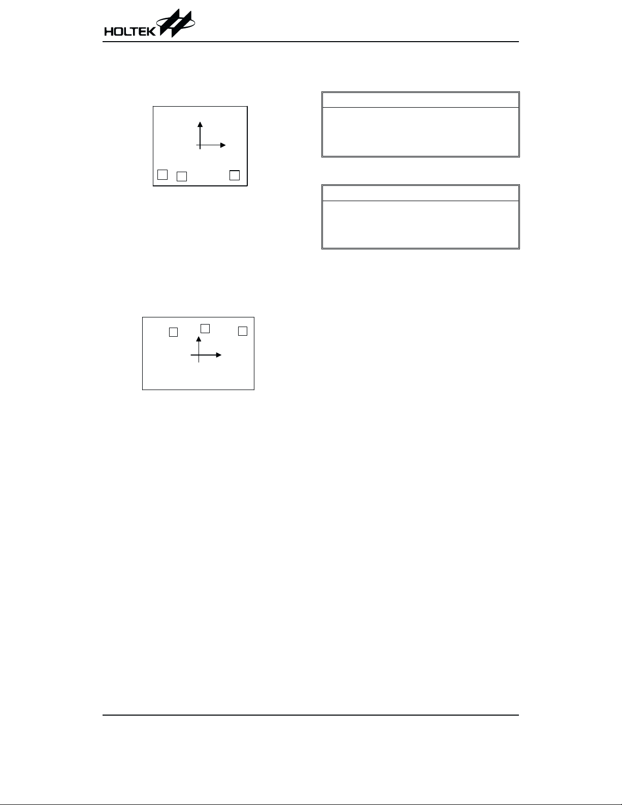
HT70XX
Pad Assignment
HT70XX (except HT7022A)
( 0 , 0 )
1
2
V O U T
V I N
Chip size: 1317 ´ 1158 (mm)
* The IC substrate should be connected to VDD in the
PCB layout artwork.
HT7022A only
O U T
1
( 0 , 0 )
3
G N D
2
V D D
2
V S S
3
Pad Coordinates
HT70XX (except HT7022A)
Pad No. X Y
1
2
3 443.90
HT7022A only
Pad No. X Y
1
2 120.65 461.01
3 774.70 412.75
-483.30 -379.50
-234.60 -399.50
-434.34
Unit: mm
-386.00
Unit: mm
394.97
Chip size: 2032 ´ 1321 (mm)
2
* The IC substrate should be connected to VDD in the
PCB layout artwork.
Absolute Maximum Ratings
Supply Voltage, except HT7022A..................................................................................................VSS-0.3V toVSS+26V
Supply Voltage, HT7022A only....................................................................................................................-0.3V to13V
Output Voltage...........................V
Storage Temperature ............................-50°Cto125°C Power Consumption ..........................................200mW
Operating Temperature...............................0°Cto70°C
Note: These are stress ratings only. Stresses exceeding the range specified under ²Absolute Maximum Ratings² may
cause substantial damage to the device. Functional operation of this device at other conditions beyond those
listed in the specification is not implied and prolonged exposure to extreme conditions may affect device reliabil
ity.
-0.3V to VDD+0.3V Output Current......................................................50mA
SS
-
Rev. 1.60 3 January 14, 2003
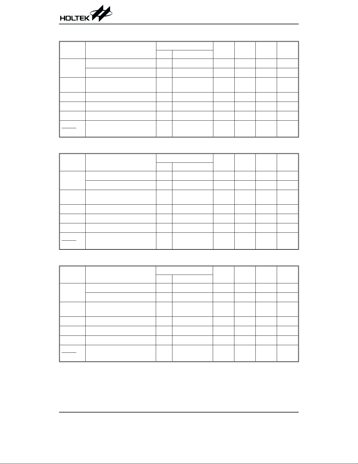
Electrical Characteristics
HT7022A
HT70XX
Ta=25°C
Symbol Parameter
V
V
I
DD
V
I
OL
DDV
DET
HYS
DD
DET
T
Hi®Lo Detectable Voltage ¾¾
Lo®Hi Detectable Voltage ¾¾
Hysteresis Width
Operating Current 3.2V No load
Operating Voltage
Output Sink Current 2V
Temperature Coefficient
a
HT7024A
Symbol Parameter
V
V
I
DD
V
I
OL
DDV
DET
HYS
DD
DET
T
Hi®Lo Detectable Voltage ¾¾
Lo®Hi Detectable Voltage ¾¾
Hysteresis Width
Operating Current 8V No load
Operating Voltage
Output Sink Current 2V
Temperature Coefficient
a
Test Conditions
DD
Conditions
V
Min. Typ. Max. Unit
2.09 2.2 2.31 V
2.132 2.31 2.541 V
¾¾
¾¾
=0.2V
V
OUT
0.02
V
DET
¾
1.6
0.5 1
0.05
V
DET
1.8 4
¾
0.1
V
DET
12 V
¾
mA
mA
¾ 0°C<Ta<70°C ¾±0.9 ¾ mV/°C
Ta=25°C
Test Conditions
DD
Conditions
V
Min. Typ. Max. Unit
2.28 2.4 2.52 V
2.325 2.52 2.772 V
¾¾
¾¾
=0.2V
V
OUT
0.02
V
DET
¾
1.5
0.5 1
0.05
V
DET
47
¾
0.1
V
DET
24 V
¾
mA
mA
¾ 0°C<Ta<70°C ¾±0.9 ¾ mV/°C
V
V
HT7027A
Symbol Parameter
V
V
I
DD
V
I
OL
DDV
DET
HYS
DD
DET
T
Hi®Lo Detectable Voltage ¾¾
Lo®Hi Detectable Voltage ¾¾
Hysteresis Width
Operating Current 8V No load
Operating Voltage
Output Sink Current 2V
Temperature Coefficient
a
Test Conditions
DD
Conditions
V
Min. Typ. Max. Unit
2.565 2.7 2.835 V
2.616 2.835 3.118 V
¾¾
¾¾
=0.2V
V
OUT
0.02
V
DET
¾
1.5
0.5 1
0.05
V
DET
V
47
¾
¾ 0°C<Ta<70°C ¾±0.9 ¾ mV/°C
Ta=25°C
0.1
DET
24 V
¾
V
mA
mA
Rev. 1.60 4 January 14, 2003
HT70XX
HT7033A
Symbol Parameter
V
V
I
DD
V
I
OL
DDV
DET
HYS
DD
DET
T
Hi®Lo Detectable Voltage ¾¾
Lo®Hi Detectable Voltage ¾¾
Hysteresis Width
Operating Current 8V No load
Operating Voltage
Output Sink Current 2.5V
Temperature Coefficient
a
HT7039A
Symbol Parameter
V
V
I
DD
V
I
OL
DDV
DET
HYS
DD
DET
T
Hi®Lo Detectable Voltage ¾¾
Lo®Hi Detectable Voltage ¾¾
Hysteresis Width
Operating Current 8V No load
Operating Voltage
Output Sink Current 2.5V
Temperature Coefficient
a
Ta=25°C
Test Conditions
DD
Conditions
V
Min. Typ. Max. Unit
3.135 3.3 3.465 V
3.197 3.465 3.811 V
¾¾
¾¾
=0.25V
V
OUT
0.02
V
DET
V
¾
1.5
1.2 2.5
0.05
DET
47
¾
0.1
V
DET
24 V
¾
V
mA
mA
¾ 0°C<Ta<70°C ¾±0.9 ¾ mV/°C
Ta=25°C
Test Conditions
DD
Conditions
V
Min. Typ. Max. Unit
3.705 3.9 4.095 V
3.779 4.095 4.504 V
¾¾
¾¾
=0.25V
V
OUT
0.02
V
DET
V
¾
1.5
1.2 2.5
0.05
DET
47
¾
0.1
V
DET
24 V
¾
V
mA
mA
¾ 0°C<Ta<70°C ¾±0.9 ¾ mV/°C
HT7044A
Symbol Parameter
V
V
I
DD
V
I
OL
DDV
DET
HYS
DD
DET
T
Hi®Lo Detectable Voltage ¾¾
Lo®Hi Detectable Voltage ¾¾
Hysteresis Width
Operating Current 8V No load
Operating Voltage
Output Sink Current 3.6V
Temperature Coefficient
a
Test Conditions
DD
Conditions
V
Min. Typ. Max. Unit
4.18 4.4 4.62 V
4.263 4.62 5.082 V
¾¾
¾¾
=0.36V
V
OUT
0.02
V
DET
¾
1.5
0.05
V
DET
47
¾
36
0.1
V
¾ 0°C<Ta<70°C ¾±0.9 ¾ mV/°C
Ta=25°C
DET
24 V
¾
mA
V
mA
Rev. 1.60 5 January 14, 2003

HT70XX
HT7050A
Symbol Parameter
V
V
I
DD
V
I
OL
DDV
DET
HYS
DD
DET
T
Hi®Lo Detectable Voltage ¾¾
Lo®Hi Detectable Voltage ¾¾
Hysteresis Width
Operating Current 8V No load
Operating Voltage
Output Sink Current 3.6V
Temperature Coefficient
a
HT7070A
Symbol Parameter
V
V
I
DD
V
I
OL
DDV
DET
HYS
DD
DET
T
Hi®Lo Detectable Voltage ¾¾
Lo®Hi Detectable Voltage ¾¾
Hysteresis Width
Operating Current 8V No load
Operating Voltage
Output Sink Current 5V
Temperature Coefficient
a
Ta=25°C
Test Conditions
V
DD
Conditions
Min. Typ. Max. Unit
4.75 5 5.25 V
4.845 5.25 5.775 V
¾¾
¾¾
=0.36V
V
OUT
0.02
V
DET
¾
2.1
0.05
V
DET
47
¾
36
0.1
V
DET
24 V
¾
V
mA
mA
¾ 0°C<Ta<70°C ¾±0.9 ¾ mV/°C
Ta=25°C
Test Conditions
V
DD
Conditions
Min. Typ. Max. Unit
6.65 7 7.35 V
6.783 7.35 8.085 V
¾¾
¾¾
=0.5V
V
OUT
0.02
V
DET
¾
2.1
0.05
V
DET
47
¾
510
0.1
V
DET
24 V
¾
V
mA
mA
¾ 0°C<Ta<70°C ¾±0.9 ¾ mV/°C
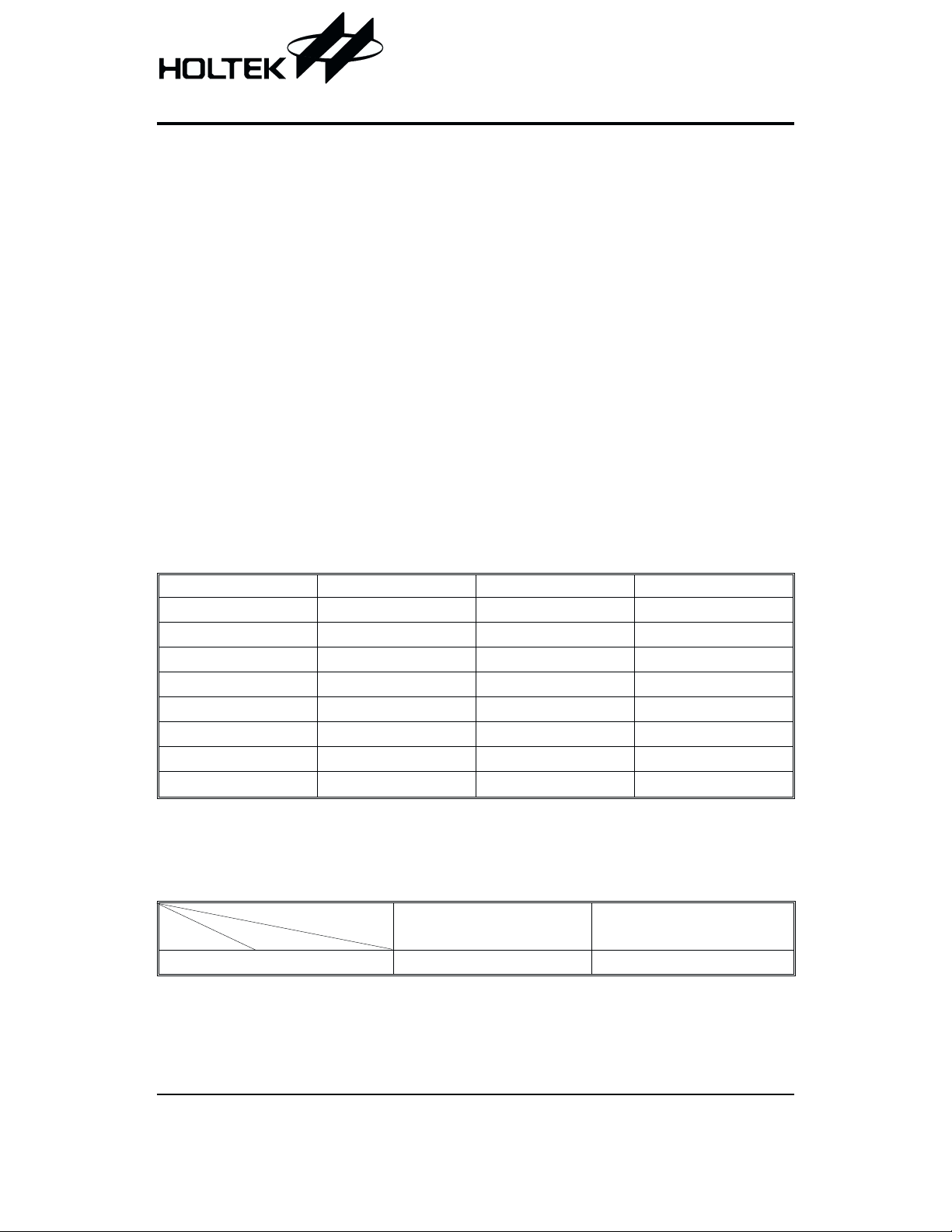
Functional Description
The HT70XX series is a set of voltage detectors
equipped with a high stability voltage reference which is
connected to the negative input of a comparator¾ de
noted as V
in the following figure for NMOS output
REF
voltage detector.
When the voltage drop to the positive input of the com
parator (i,e,V
M1 turns off, and V
(R
B+RC
falls to a value less than V
verts from high to low, V
) is higher than V
B
is expressed as VBH=VDD´
B
)/(RA+RB+RC). If VDDis decreased so that V
REF
OUT
turns on, RC is bypassed, and V
V
BL=VDD´RB
/(RA+RB), which is less than V
, VOUT goes high,
REF
, the comparator output in
goes low, VCis high, M1
becomes:
B
By so
BH.
doing, the comparator output will stay low to prevent the
circuit from oscillating when V
» V
B
REF.
Rev. 1.60 6 January 14, 2003
If VDDfalls below the minimum operating voltage, the
output becomesundefined. When VDD goes from low to
-
V
´ RB/(RA+RB)>V
DD
V
goes high.
OUT
, the comparator output and
REF
The detectable voltage is defined as:
V
DET
The release voltage is defined as:
B
V
DET
RRR
ABC
(-)=
RR
AB
(+) =
++
RR
+
BC
+
´ V
R
B
REF
´ V
REF

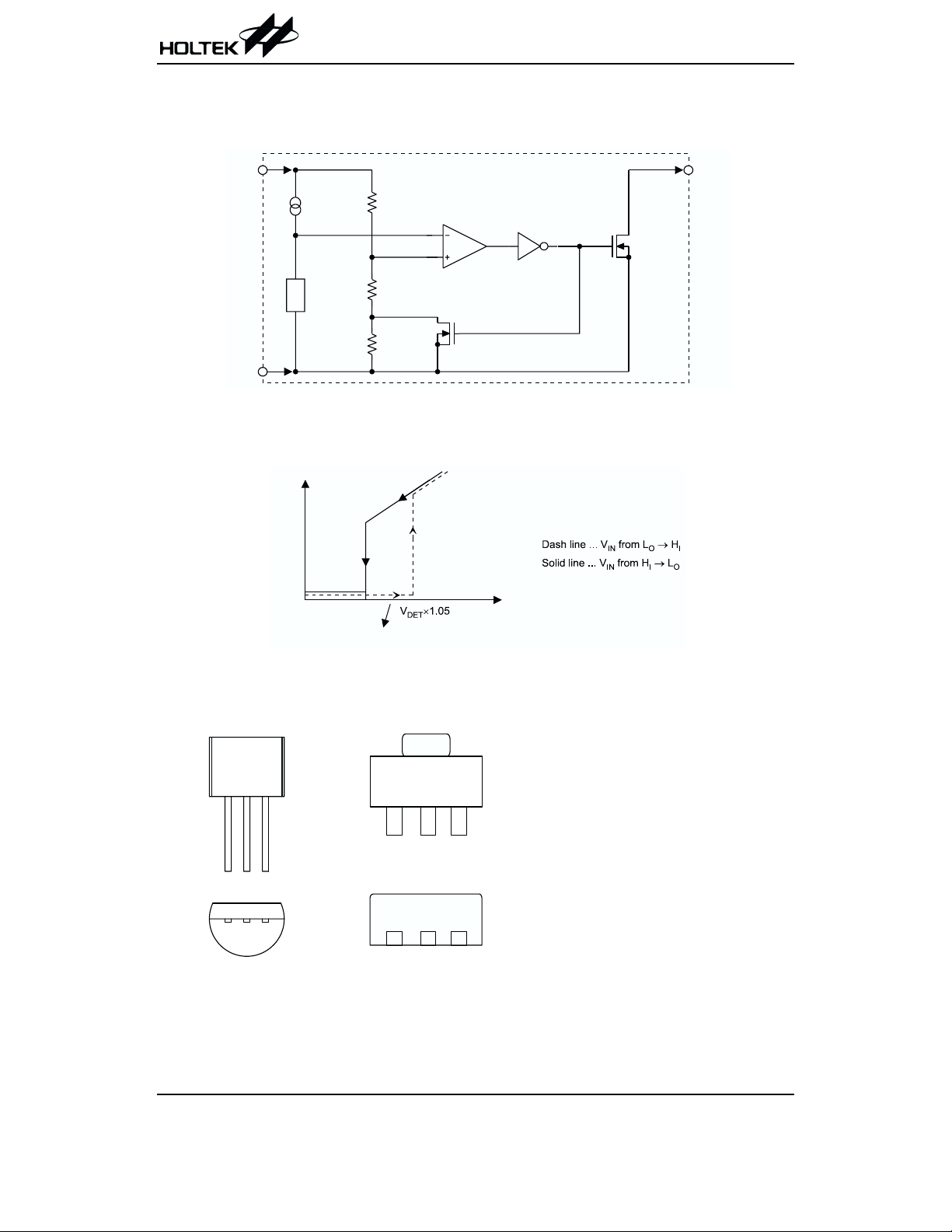
The hysteresis width is:
V
HYS=VDET
(+) - V
DET
(-)
The figure demonstrates the NMOS output type with
positive output polarity (V
is normally open, active
OUT
low). The HT70XX series also supplies options for other
output types with active high outputs. Application cir
cuits shown are examples of positive output polarity
(normally open, active low) unless otherwise specified.
Application Circuits
Microcomputer reset circuit
Normally a reset circuit is required to protect the micro
computer system from malfunctions due to power line
interruptions. The following examples show how differ
ent output configurations perform a reset function in var
ious systems.
·
NMOS open drain output application for separate
power supply
V
D D 1
H T 7 0 X X A
V
O U T
R E S E T
M i c r o c o m p u t e r
V
D D 2
V
S S
R
A
C o m p a r a t o r
V
V
B
C
-
V
R E F
R
B
M 1
R
C
NMOS output voltage detector (HT70XXA)
Power-on reset circuit
With several external components, the NMOS open
drain type of the HT70XX series can be used to perform
a power-on reset function as shown:
-
-
V
I N
R
C
D
V
D D
V
O U T
H T 7 0 4 4 A
V
S S
V
D D
HT70XX
V
D D
R L
V
O U T
M N
V
S S
V
O U T
V
S S
·
NMOS open drain output application with R-C delay
V
D D
R
H T 7 0 X X A
V
O U T
M i c r o c o m p u t e r
t
V
O U T
C
V
S S
Rev. 1.60 7 January 14, 2003

5V power line monitoring circuit
T
Generally, a minimum operating voltage of 4.5V is guar
anteed in a 5V power line system. The HT7044A is rec
ommended for use as 5V power line monitoring circuit.
·
5V power line monitor with power-on reset
5 V P o w e r l i n e
R
D
HT70XX
·
Varying the detectable voltage with a diode
V
-
-
I N
V f 1
V f 2
V
D D
V
O U T
H T 7 0 X X A
V
D D
C
V
O U
H T 7 0 4 4 A
V
S S
·
with 5V voltage regulator
V
S S
5 V V o l t a g e r e g u l a t o r
V
I N
H T 7 1 5 0
5 V
G N D
V
D D
V
O U T
H T 7 0 4 4 A
V
S S
Change of detectable voltage
If the required voltage is not found in the standard product selection table, it is possible to change it by using external resistance dividers or diodes.
·
Varying the detectable voltage with a resistance di
vider
V
I N
V
S S
Detectable Voltage = Vf1+Vf2+V
Malfunction analysis
The following circuit demonstrates the way a circuit ana
lyzes malfunctions by monitoring the variation or spike
noise of power supply voltage.
V
O U T
H T 7 0 X X A
V
S S
Charge monitoring circuit
The following circuit shows a charged monitor for protection against battery deterioration by overcharging.
When the voltage of the battery is higher than the set detectable voltage, the transistor turns on to bypass the
charge current, protecting the battery from overcharging.
V
-
S o l a r
C e l l
T r
V
D D
O U T
B A T T
DET
V
V
D D
S S
L o a d
V
S S
-
R
A
R
B
V
S S
Detectable voltage =
Hysteresis width =
RR
AB
+
R
B
RR
AB
+
R
B
V
D D
H T 7 0 X X A
´ V
DET
´ V
HYS
V
O U T
V
S S
V
S S
H T 7 0 X X A
Rev. 1.60 8 January 14, 2003

Level selector
The following diagram illustrates a logic level selector.
V D D
HT70XX
V S S
5 . 0 V
3 . 9 V
V D D
V D E T 1
V D E T 2
O U T
V O U T
H T 7 0 3 9 A
V O U T
O U T
H T 7 0 5 0 A
V D E T 1V D E T 2
t
t
Rev. 1.60 9 January 14, 2003

Package Information
3-pin TO-92 outline dimensions
HT70XX
A
B
D
C
E
F
G
H
Symbol
Min. Nom. Max.
A 170
B 170
C 500
D11
E90
F45
G45
H 130
I8
Dimensions in mil
¾
¾
¾¾
¾
¾
¾
¾
¾
¾
a 4°¾6°
200
200
20
110
55
65
160
18
Rev. 1.60 10 January 14, 2003

3-pin SOT-89 outline dimensions
HT70XX
A
B
E
G
F
Symbol
H
Dimensions in mil
Min. Nom. Max.
A 173
B64
C90
D35
E 155
F14
G17
H
¾
I55
J14
I
J
C
D
¾
¾
¾
¾
¾
¾
¾
59
¾
¾
181
72
102
47
167
19
22
¾
63
17
Rev. 1.60 11 January 14, 2003

Product Tape and Reel Specifications
TO-92 reel dimensions (Unit: mm)
HT70XX
P a c k a g e U p , F l a t S i d e U p
3 0
P a c k a g e U p , F l a t S i d e D o w n
5 8
8 8
3 6 0
4 3
Rev. 1.60 12 January 14, 2003

SOT-89 reel dimensions
HT70XX
T 2
A
B
T 1
D
SOT-89
Symbol Description Dimensions in mm
A Reel Outer Diameter
B Reel Inner Diameter
180±1.0
62±1.5
C Spindle Hole Diameter 12.75+0.15
D Key Slit Width
1.9±0.15
T1 Space Between Flange 12.4+0.2
T2 Reel Thickness
17-0.4
C
Rev. 1.60 13 January 14, 2003

TO-92 carrier tape dimensions
HT70XX
P
H 1
H
H 0
F 1 F 2
P 2
P 0
l 1
D 0
TO-92
Symbol Description Dimensions in mm
I1 Taped Lead Length (2.5)
P Component Pitch
P
P
F
F
Dh
0
2
1
2
Perforation Pitch
Component to Perforation (Length Direction)
Lead Spread
Lead Spread
Component Alignment
W Carrier Tape Width
W
W
W
H
0
H
1
D
0
Hold-down Tape Width
0
Perforation Position
1
Hold-down Tape Position (0.5)
2
Lead Clinch Height
Component Height Less than 24.7
Perforation Diameter
t Taped Lead Thickness
H Component Base Height
Note:
Thickness less than 0.38±0.05mm~0.5mm
12.7±1.0
12.7±0.3
6.35±0.4
2.5+0.4
2.5+0.4
0±0.1
18.0+1.0
6.0±0.5
9.0±0.5
16.0±0.5
4.0±0.2
0.7±0.2
19.0±0.5
P0 Accumulated pitch tolerance: ±1mm/20pitches.
( ) Bracketed figures are for consultation only
-0.1
-0.1
-0.5
h
,
W 2
W 0
W 1
W
t
Rev. 1.60 14 January 14, 2003

SOT-89 carrier tape dimensions
HT70XX
D
E
F
PD 1
P 1P 0
W
A 0
B 0
C
SOT-89
Symbol Description Dimensions in mm
W Carrier Tape Width
P Cavity Pitch
E Perforation Position
F Cavity to Perforation (Width Direction)
12.0+0.3
8.0±0.1
1.75±0.1
5.5±0.05
D Perforation Diameter 1.5+0.1
D1 Cavity Hole Diameter 1.5+0.1
P0 Perforation Pitch
P1 Cavity to Perforation (Length Direction)
A0 Cavity Length
B0 Cavity Width
K0 Cavity Depth
t Carrier Tape Thickness
4.0±0.1
2.0±0.10
4.8±0.1
4.5±0.1
1.8±0.1
0.30±0.013
C Cover Tape Width 9.3
t
K 0
-0.1
Rev. 1.60 15 January 14, 2003

HT70XX
Holtek Semiconductor Inc. (Headquarters)
No.3, Creation Rd. II, Science-based Industrial Park, Hsinchu, Taiwan
Tel: 886-3-563-1999
Fax: 886-3-563-1189
http://www.holtek.com.tw
Holtek Semiconductor Inc. (Sales Office)
11F, No.576, Sec.7 Chung Hsiao E. Rd., Taipei, Taiwan
Tel: 886-2-2782-9635
Fax: 886-2-2782-9636
Fax: 886-2-2782-7128 (International sales hotline)
Holtek Semiconductor (Shanghai) Inc.
7th Floor, Building 2, No.889, Yi Shan Rd., Shanghai, China
Tel: 021-6485-5560
Fax: 021-6485-0313
http://www.holtek.com.cn
Holtek Semiconductor (Hong Kong) Ltd.
RM.711, Tower 2, Cheung Sha Wan Plaza, 833 Cheung Sha Wan Rd., Kowloon, Hong Kong
Tel: 852-2-745-8288
Fax: 852-2-742-8657
Holmate Semiconductor, Inc.
48531 Warm Springs Boulevard, Suite 413, Fremont, CA 94539
Tel: 510-252-9880
Fax: 510-252-9885
http://www.holmate.com
Copyright Ó 2003 by HOLTEK SEMICONDUCTOR INC.
The information appearing in this Data Sheet is believed to be accurate at the time of publication. However, Holtek as
sumes no responsibility arising from the use of the specifications described. The applications mentioned herein are used
solely for the purpose of illustration and Holtek makes no warranty or representation that such applications will be suitable
without further modification, nor recommends the use of its products for application that may present a risk to human life
due to malfunction or otherwise. Holtek reserves the right to alter its products without prior notification. For the most
up-to-date information, please visit our web site at http://www.holtek.com.tw.
-
Rev. 1.60 16 January 14, 2003
 Loading...