

HT6513
Mouse Controller
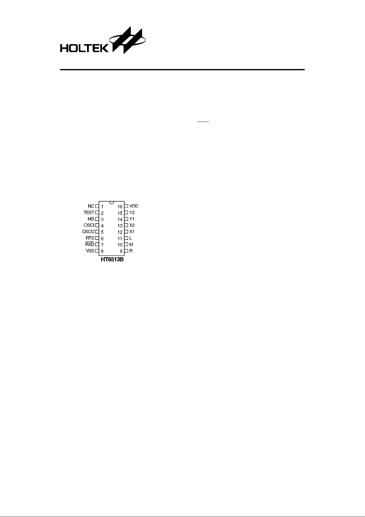
Pin Assignment
Features
•
Low power dissipation
•
Use 32.768KHz crystal
•
Crystal oscillator circuits on-chip
•
1200 baud rate serial output
•
Power directly from RS-232C without external power supply
•
Three key-switches a nd four photo-couples
inputs
•
Key-in and key-release debounce interval 52 ms
•
The HT6513 can execute two different
outputs with any of the key-switch inputs
•
RXD with heavy NMOS output
General Description
The HT6513 is a specially designed CMOS IC
for mouse control applications. Capable of driving up to 3 key-switches a nd 4 photo-couplers
directly into a standard RS-232C line, and it
can be operated without an external power supply. It is compatible with both Microsoft and
Mouse systems with false entries being prevented by internal debounce circuits.
1 23rd Oct ’96
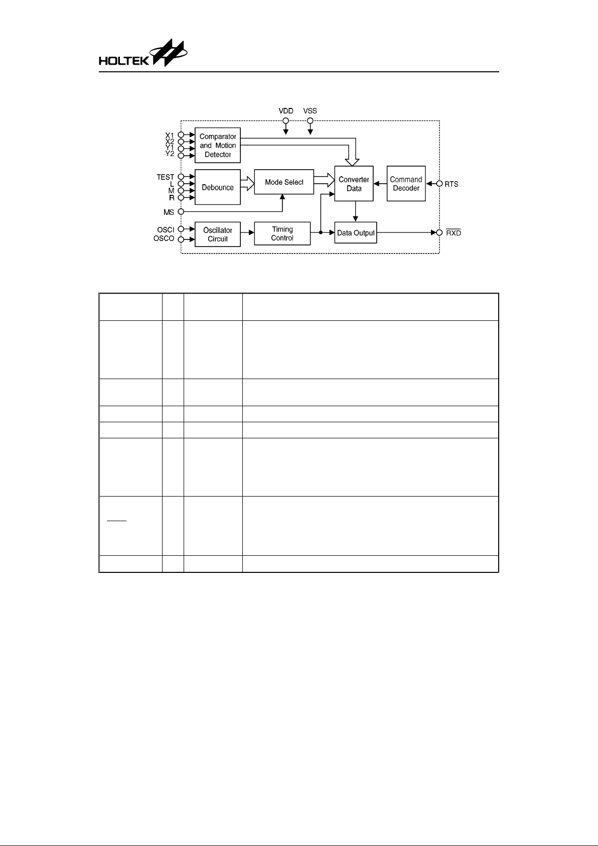
Block Diagram
Pin Description
Pin Name I/O
Internal
connection
Description
MS I —
When this pin is connected to VDD , then HT65 13 is assi gned
to operate under the microsoft mode only. If the pin is
connected to VSS, then HT6513 wi ll ope rate under th e m ouse
system mode. If MS pin is “floating”, the HT6513 is on the
power on initiation mode.
TEST I Pull-Low
For IC test only. The test pin must be connected to VSS, while
the chip is under normal usage.
OSCI I — Oscillator input pin
OSCO O — Oscillator output pin
RTS I —
The signal is sent b y the mouse driver from the computer to
select the mode.
The HT6513 re plies with the selected m ode to the RXD line
after the puls e signal of the RTS l ine. RXD wi ll send out “ CD”H
code under the microsoft mode.
RXD O
NMOS
Open Drain
There are 7 or 8 bits in each data byte. Using p arallel-in and
serial-out circuit, the data bytes are shifted out from bit 0
through the most significant bit. HT6513 will transmit the
data when the s tatus of the three ke y-switches or the state of
the horizontal counter or vertical counter change.
VSS I — Negative power supply
HT6513
2 23rd Oct ’96
Pin Name I/O
Internal
connection
Description
R
M
L
IPull-Low
Three key-switches have seven different combinations in total.
Both key-pressed and key-released signals will be sent
accompanied with horizo ntal and ve rtical state. The status of
the key-switches, the value s of h orizon tal or ve rtical co unters
will be present at RXD and
RXD. The debounce interval for
both key-press and key-release is 13ms.
X1
X2
Y1
Y2
I—
Four photo-couplers signals denote UP, DOWN, LEFT, and
RIGHT state.
During the scaning period, as long as the photo-couplers
change their states, the value of vertical or horizon tal counte r
will increase or decrease accordingly.
VDD I — Position power supply
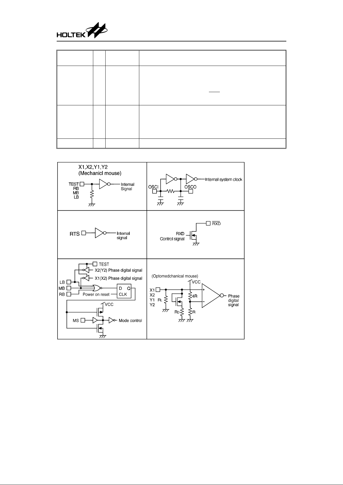
Approximate Internal connection circuits
HT6513
3 23rd Oct ’96
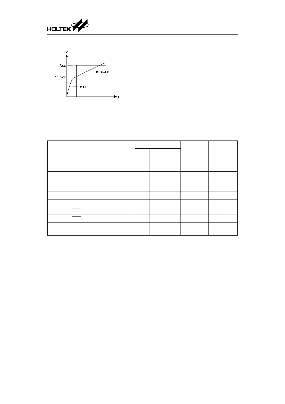
X1/X2/Y1/Y2 Input pin I/V curve (optomechanical mouse)
Absolu te Maxim u m Rating s
Supply Voltage.................................–0.3V to 7V Storage Temperature.................–50°C to 125°C
Input Voltage.................... V
SS
–0.3V to VDD+0.3 Operating Temperature...............–20°C to 75°C
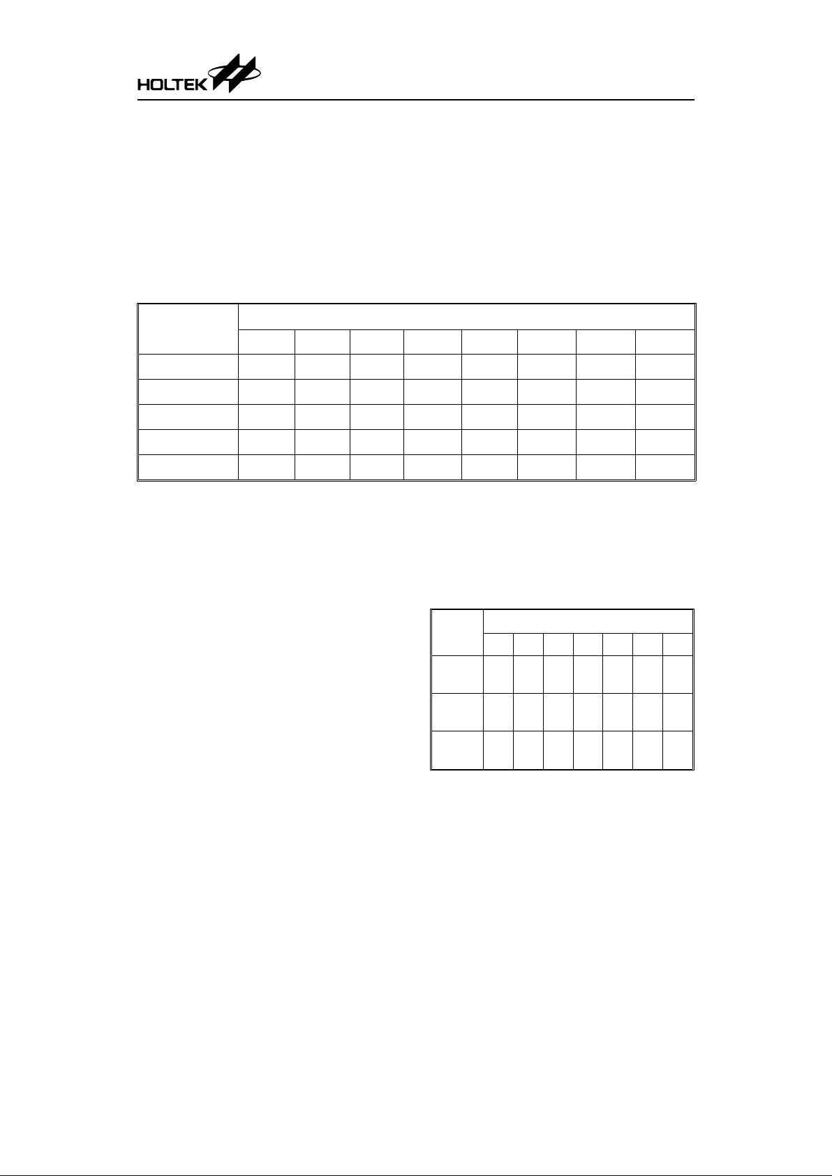
D.C. Characteristics (Ta=25°C)
Symbol Parameter
Test condition
Min. Typ. Max. Unit
V
DD
Condition
V
DD
Operating voltage — — 4.0 5.1 6.1 V
I
DD
Operating current 5.6V No load — 400 760 µA
V
IL
X1,X2,Y1,Y2 Input low voltage 5.6V — 0 — 1.1 V
V
IH
X1,X2,Y1,Y2
Input high voltage
5.6V — 1.8 — 5.6 V
V
IL1
Input low voltage, other pin 5.6V — 0 — 1 V
V
IH1
Input high voltage, other pin 5.6V — 3.5 — 5.6 V
I
OL
RXD output sink current 5.6V VOL=0.56V 3.5 6 — mA
V
OH
RXD high-level output voltage — — — — 16 V
R
PL
Pull-low resistance 5.6V
L, M, R
key-switches
65 — 200 KΩ
HT6513
4 23rd Oct ’96

A.C. Characteristics (Ta=25°C)
Symbol Parameter
Test Condition
Min. Typ. Max. Unit
V
DD
Condition
f
SYS
System Clock 5.6V Crystal Oscillator 30.8 32.768 34.2 KHz
f
P
Photo-Couple input
frequency
5.6V — — — 8.2 KHz
f
N
Photo-Couple operation
frequency
5.6V — 0 — 8 KHz
t
KD
Key debounce 5.6V — — 52 — ms
t
MS
Transmission time 5.6V
mouse system
(1200 bps)
— 41.3 — ms
t
MI
Transmission time 5.6V microsoft (1200 bps) — 24.8 — ms
t
S
Start bit time 5 .6 V (1200 bps) — 0.85 — ms
t
D
Data bit time 5.6V (1200 bps) — 0.82 — ms
t
P
Stop bit time 5.6V (1200 bps) — 0.82 — ms
t
RD
Mode code delay
Time (f
SYS
=32.768KHz)
5.6V (1200 bps) 11 . 9 — 14 ms
t
R
Rising edge
crossed width
5.6V — 31 — —
µs
t
F
Falling edge
crossed width
5.6V — 31 — —
µs
HT6513
5 23rd Oct ’96
Output word format:
Bit No.
Mouse system word structures
76543210
1st word 1 0 0 0 0 L’ M’ R’
2nd word H7 H6 H5 H4 H3 H2 H1 H0
3rd word V7 V6 V5 V4 V3 V2 V1 V0
4th word EH7 EH6 EH5 EH4 EH3 EH2 EH1 EH0
5th word EV7 EV6 EV5 EV4 EV3 EV2 E V1 EV0
’: denotes com ple ment
H0~H7: The values of horizontal counter.
V0~V7: The values of vertical counter.
EH0~EH7: The values of extra horizontal counter.
EV0~EV7: The values of extra vertical counter.
Microsoft system mode
In the microso ft mode only 3 wo rds are transmitted with each word divided into one start
bit, seven data bits and two stop bits. Note that
only 2 switch operation is available with the
“M” switch being redu ndant in this mod e. The
“L” and “R” switch status together with the two
most significant b its of both vertical a nd horizontal counters are transferred in this first
word. The second and third word represent the
horizontal and vertical counters respectively.
Note that this verti cal data is recorded in 2’s
complement format.
Output word format:
Bit
No.
Mouse system word structures
6543210
1st
word
1LRV7’V6’H7H6
2nd
word
0 H5H4H3H2H1H0
3rd
word
0 V5’ V4’ V3’ V2’ V1’ V0’
Function Descriptions
Mouse system mode
Any change of state of the mo use key-switches
or photo-couplers will be detected by the
HT6513 and transmitted over the RS-232C.
The mouse system protocol will send five words
at a 1200 baud rate wi th each word contai ning
10 bits, one start bit, one stop bit and eight data
bits. The first, second and third words corre-
spond to key switch -status, horizontal counter
and vertical counter respectively. The autospeed sensing circuits ensure detection of
higher mouse speeds resulting in the use of t he
4th and 5th words for extra horizontal and vertical overflow counts respectively. For lower
mouse speeds the 4th and 5th words rema in at
zero.
HT6513
6 23rd Oct ’96

Timing Diagrams
HT6513
7 23rd Oct ’96

Application Circuit
RXD output
HT6513
8 23rd Oct ’96
 Loading...