

Infrared Remote Encoder
Features
Operating voltage: 2.2V~3.6V
·
Low power consumption
·
Few external parts
·
Applications
Television and video cassette recorder
·
controllers
Garage door controllers
·
General Description
HT6240-002 is designed as infrared remote
encoders, usually applied to TV systems. The
4´8 key matrix input and the extension bit in
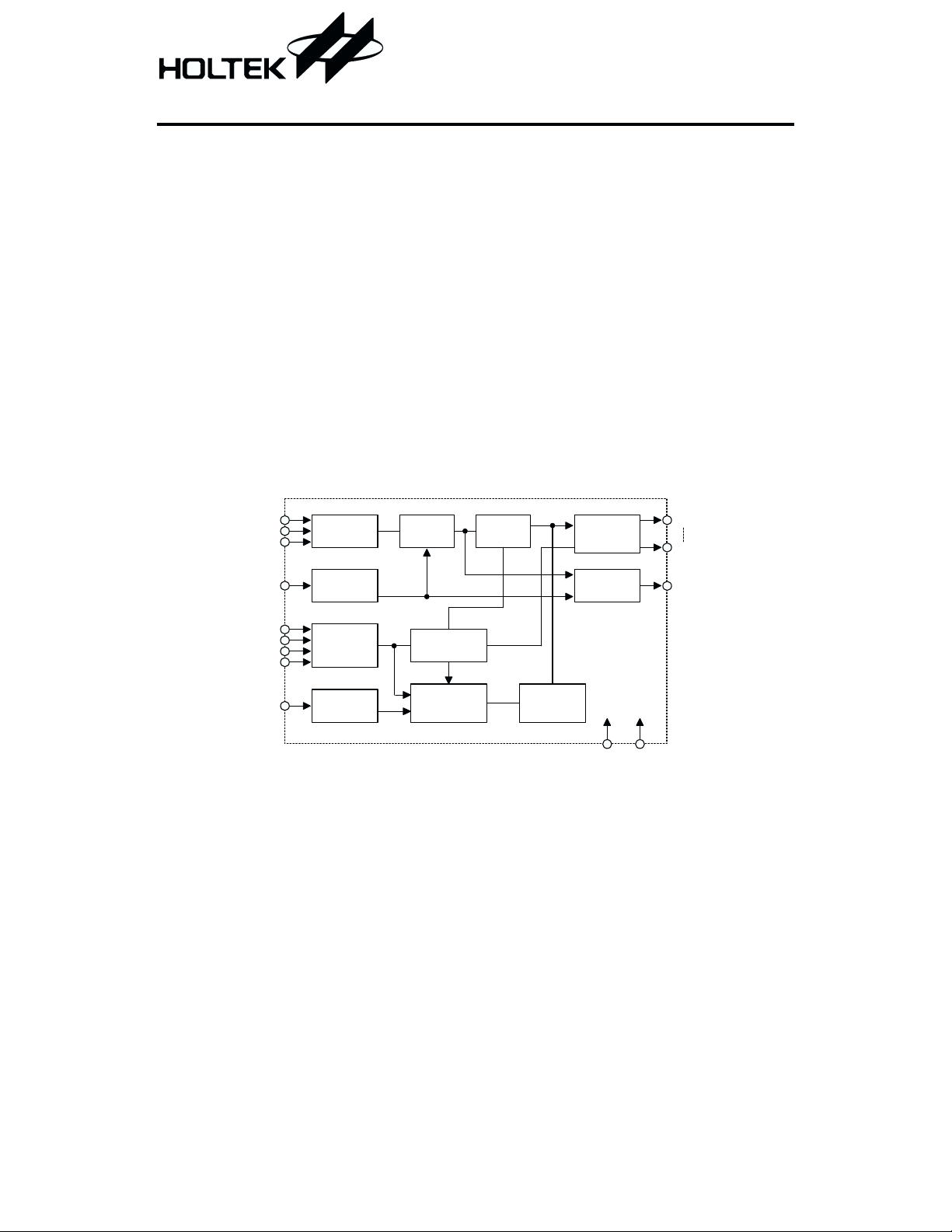
Block Diagram
HT6240-002
20-pin DIP/SOP package
·
24-pin SOP package
Car door controllers
·
Security systems
·
Other remote control systems
·
put can transmit a max. of 256 instructions.
HT6240-002 have three different packages:
20-pin DIP, 20-pin SOP and 24-pin SOP.
-
PRB
OSCI
OSCO
TEST
IE 0
IE 1
IE 2
IE 3
DATA
OSC
TEST
MODE
IE -K E Y
Encoder
8-B it S hift
R egister
2
3´2
D u ty 1 /3
C ontrol
Unit
C ustom C ode
& D A TA C ode
Latch
8
10´2
D ivider
P a ra lle l to
C onverter
1 December 16, 1999
Serial
Key Scan
Driver
D ecoder
O utput
Stage
VDD VSS
OF0
OF7
CT
Pin Assignment
1
VSS
TEST
PRB
OSCI
OSCO
DATA
IE 0
IE 1
IE 2
IE 3
2
3
4
5
6
7
8
9
10
H T6240-002
20 DIP/SO P
20
19
18
17
16
15
14
13
12
11
VDD
CT
OF0
OF1
OF2
OF3
OF4
OF5
OF6
OF7
VSS
TEST
PRB
OSCI
OSCO
DATA
IE 0
IE 1
IE 2
IE 3
NC
NC
1
2
3
4
5
6
7
8
9
10
11
12
24
23
22
21
20
19
18
17
16
15
14
13
H T6240-002
2 4 S O P
HT6240-002
VDD
CT
OF0
OF1
OF2
OF3
OF4
OF5
OF6
OF7
NC
NC
Pad Assignment
* The IC substrate should be connected to VDD in the PCB layout artwork.
PRB
OSCI
OSCO
DATE
IE 0
IE 1
TES T
VSS
19
20
1
2
3
4
5
6
7178
IE 2
Chip size: 92 ´ 118 mil
18
VDD
(0 ,0 )
9
IE 3
OF7
10
OF6
2
CT
16
15
14
13
12
11
OF0
OF1
OF2
OF3
OF4
OF5
2 December 16, 1999
Pad Coordinates Unit: mil
Pad No. X Y Pad No. X Y
1
2
3
4
5
6
7
8
9 9.22
10 24.40
-40.88
-40.88
-40.88 -11.56
-40.88 -24.78
-40.88 -34.04
-40.88 -41.18
-13.77 -52.78
-7.14 -52.78
16.11 11 40.12
9.48 12 40.12
13 40.12
14 40.12
15 40.12
16 40.12 7.78
17 34.47 53.59
-53.55
-53.55
18
19
20
-8.97
-15.60
-22.23
-48.32
-39.74
-24.57
-15.98
-0.81
53.59
53.59
52.02
Pad Description
HT6240-002
Pad No. Pad Name I/O
1 PRB I
2 OSCI I CMOS Oscillator input
3 OSCO O CMOS Oscillator output
4 DATA I/O
5~8 IE0~IE3 I
9~16 OF7~OF0 O NMOS Drive for key scan
17 CT O CMOS Generates output transmission code
18 VDD
19 VSS
20 TEST I CMOS
¾¾
¾¾
Internal
Connection
CMOS
Pull-high
CMOS, NMOS
Pull-high
CMOS
Pull-high
Description
Power on reset
Detect custom code and extended code
Detect input from key matrix
Positive power supply
Negative power supply
TEST=Low normal mode
TEST=High test mode
3 December 16, 1999
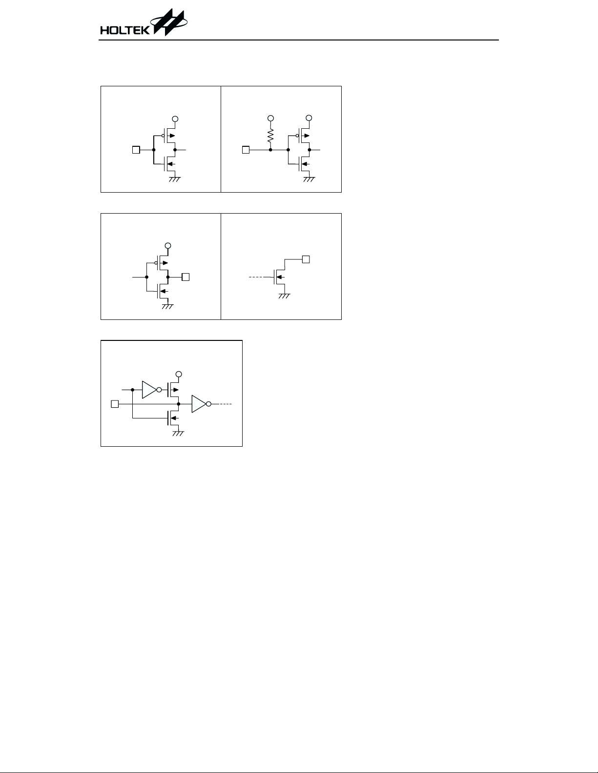
Approximate internal connection circuits
In p u t te rm in a l
P in : T E S T , O S C I P in : P R B , IE 0 ~ IE 3
V
DD
O u tp u t te rm in a l
P in : O S C O , C T Pin: OF0~OF7
V
DD
HT6240-002
V
V
DD
DD
Bidirectional term inal
P in : D A T A
V
DD
Absolute Maximum Ratings
Supply Voltage ..............................-0.3V to 5.2V
Output Voltage..................................V
SS
to V
DD
Operating Temperature...............-20°Cto70°C
Note: These are stress ratings only. Stresses exceeding the range specified under ²Absolute Maxi
mum Ratings² may cause substantial damage to the device. Functional operation of this de
vice at other conditions beyond those listed in the specification is not implied and prolonged
exposure to extreme conditions may affect device reliability.
Input Voltage ......................V
-0.3 to VDD+0.3
SS
Storage Temperature.................-40°Cto125°C
4 December 16, 1999
-
-
HT6240-002
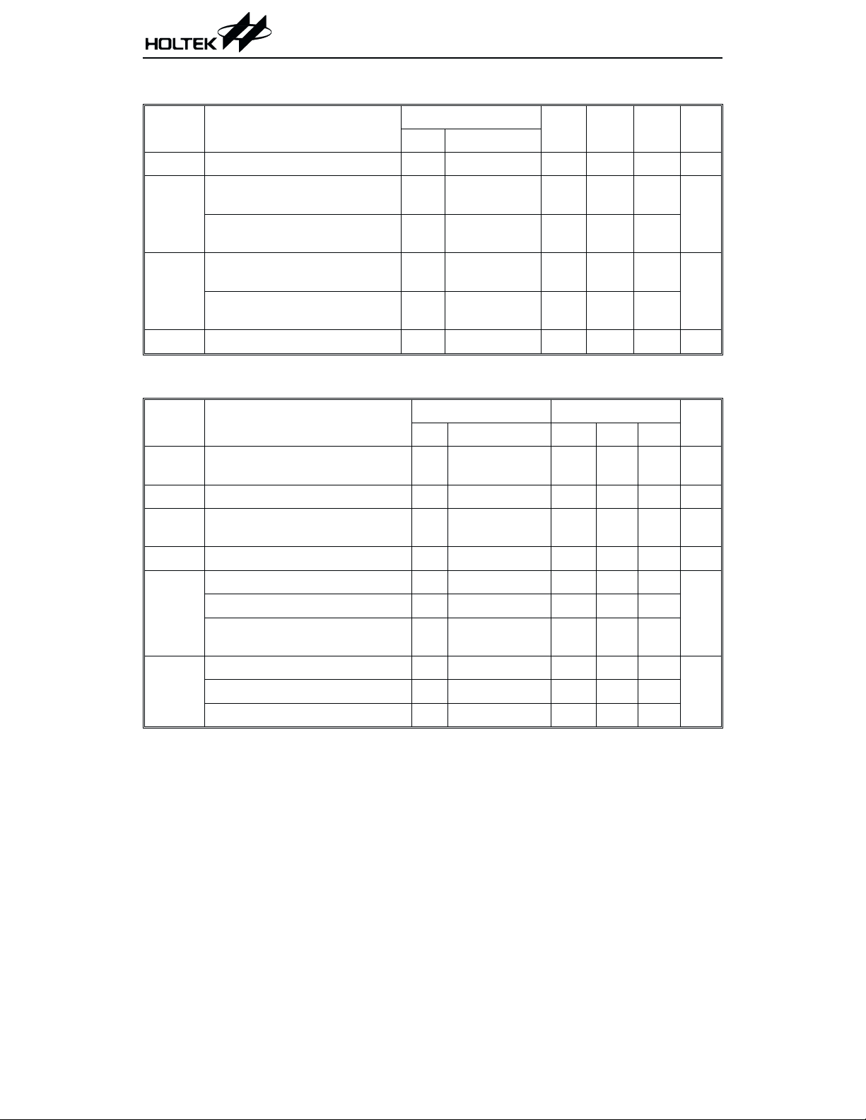
Recommended Operating Condition
Symbol Parameter
V
DD
Supply Voltage
High-level Input Voltage
V
IH
IE0~IE3, DATA
High-level Voltage PRB
Low-level Input Voltage
V
IL
IE0~IE3, DATA
Low-level Input Voltage PRB
f
OSC
Clock Oscillating Frequency 3V
Electric Characteristics
Symbol Parameter
V
DD
I
DD
I
DD
I
OH
I
OL
R
I
Supply Voltage
Supply Current (during operation) 3V
Supply Current
(while not in operation)
High-level Output Current CT 3V
Low-level Output Current CT 3V
Low-level Output Current DATA 3V
Low-level Output Current
OF0~OF7
Pull-up Resistance PRB 3V
Pull-up Resistance DATA 3V
Pull-up Resistance E0~E3 3V
Ta= -20°C~70°C, unless otherwise noted
Test Conditions
Min. Typ. Max. Unit
V
Conditions
DD
¾¾
3V
3V
3V
3V
¾
¾
¾
¾
¾¾
2.2
¾
3.6 V
2.4V 3V 3V
2.1V 3V 3V
0 0 1.2V
0 0 0.9V
455
¾
Ta=25°C, VDD=3V, VSS=0V, unless otherwise noted
Test Conditions Limits
V
Conditions Min. Typ. Max.
DD
f
=455kHz,
OSC
¾
Ta=-20°C~70°C
f
OSC
3V
V
OH
V
OL
V
OL
V
3V
OL
=455kHz
¾¾¾1mA
=2V
=0.9V
=0.9V
=0.9V
2.2
¾
-5 -10 ¾
0.3 0.8
14
14
3.6 V
¾
0.1 0.3 mA
¾
¾
¾
¾¾80¾
¾¾70¾
¾¾70¾
V
V
kHz
Unit
mA
mA
kW
5 December 16, 1999

Functional Description
HT6240-002
Key operation
The input pins (IE0~IE3) and the output pins
(OF0~OF7) constitute a max. of 4´8 key matrix
which is also called standard key. The extended
key is formed by input pin DATA and the scan
output (OF5~OF7). The 4´8 key matrix and the
extended key can transmit a max. of 256 in
struction.
CT maintains ²L² and no transmission code is
generated when two or more keys in standard
key are pressed.
Table 1 shows the relationship between the key
matrix and the transmission code.
Table 1
Transmission Code
Key Input
D1 D0
IE0 00
IE1 01
IE2 10
IE3 11
Transmission Code
Scan Output
D4 D3 D2
OF0 000
OF1 001
OF2 010
OF3 011
OF4 100
OF5 101
OF6 110
OF7 111
Custom code
The custom code is made up of input pin DATA
and scan output OF0~OF4. It has 8 bits
(C0~C7); the lower 3 bits of the custom code
(C5, C6 and C7) are fixed as ²0².
Fig. 1 shows an example of custom code selection.
-
DATA O F0 O F1 O F2 O F3 O F4
C ustom code
C01C11C20C30C41C50C60C7
Fig. 1
Extended bit
The extended bit is formed by input pin DATA
and the scan output (OF5~OF7). Fig. 2 shows
an example of extended bit selection.
DATA
D A T A code
SW =ON
SW =OFF
OF5 OF6 OF7
D5
D6
1
1
1
0
0
D7
0
0
Transmission Code
DATA Input
OF5
OF6
OF7 1
D7 D6 D5
¾¾
¾
1
1
¾
¾¾
SW
Fig. 2
6 December 16, 1999

HT6240-002
Clock oscillating circuit
HT6240 has built-in feedback resistor and
CMOS inverter, so a ceramic resonator can con
nect between the oscillator circuit input pin
(OSCI) and the output pin (OSCO), (see Fig. 3).
When the ceramic resonator is set to 455kHz,
the carrier can be set 38kHz.
The oscillating circuit will stop when there is no
key pressed to save power dissipation.
H T6240-002
OSCI OSCO
C
LI
N ote: T hese capacitors depend on the resonators.
U se the values recom m ended by the resonator
m anufacturer.
Fig. 3
26.4m s
8.8m s
C
LO
Transmission code
When the resonator is 455kHz, the carrier of
the transmission signal is 38kHz. One pulse
width is 0.53ms. Therefore, twenty 38kHz
clocks are included in the 0.53ms pulse width.
(Fig.4 shows the carrier)
HT6240-002 has two different formats. When
the custom code is equal to zero, CT will send
the 1st format. Otherwise, it will send the 2nd
format.
If the custom code (C0~C7) is ²0000 0000² then
Fig. 5 shows the formation of the transmission
code. Fig. 6 shows the transmission code ²0²
and ²1² and pulse width. Fig. 7 shows the for
mation of the 1-word transmission code. If a le
gal key is pressed, HT6240-002 will send at
least five words (see Fig. 8).
-
-
Fig. 4 Carrier
D0 D1 D2 D3 D4 D5
D ata code
Fig. 5 Formation of the transmission code
0.53m s
0.53m s
B it "0 "
2.11m s
0.53m s
B it "1 "
4.22m s
Fig. 6 Transmission code ²0² and ²1² and
pulse width of HT6240-002
7 December 16, 1999

HT6240-002
On table 2, the relationship between the key
matrix and the transmission code is shown when
custom code=²0000 0000². The asterisks means
that HT6240-002 can just send five words at a
time even if a legal key is pressed for a long
time. The others mean that HT6240-002 will
send five or six words, even some more words if
a legal key is still pressed.
Table 2
OF0 OF1 OF2 OF3 OF4 OF5 OF6 OF7
IE0 00 04 08 0C 10* 14* 18* 1C*
IE1 01 05 09* 0D* 11* 15* 19* 1D*
IE2 02 06 0A* 0E* 12* 16* 1A* 1E*
IE3 03 07 0B* 0F* 13* 17* 1B* 1F*
D0 D1 D2 D3 D4 D5
1 w ord
50.6m s
Fig. 7 The formation of the 1-word transmission code
There are 64 instructions when the custom
code=²0000 0000² in HT6240-002. The trans
mission output CT is still ²L² and the transmis
sion code will not be sent when two or more keys
are pressed simultaneously.
If custom code ¹²0000 0000² then Fig. 9 shows
the formation of the transmission code. The
transmission code consists of a head pulse, 8-bit
custom code and 8-bit data code. Fig. 10 shows
bit ²0² and bit ²1².
The formation of a 1-word transmission code
without carrier is shown in detail in Fig.11.
Output CT should combine with the carrier when
CT is high.
-
-
1-w ord
50.6m s
1-w ord
50.6m s
1-w ord
50.6m s 50.6m s
1-w ord 1-w ord
Fig. 8 A legal key will send at least five words
8.44m s
H ead pulse
4.22m s 4.22m s
C0C1C2 C3 C4 C5C6C7 D0D1 D2 D3 D4D5D6 D7
C ustom code D ata code
Fig. 9 The formation of the transmission code when custom code ¹²0000 0000²
8 December 16, 1999

HT6240-002
CT will send at least three words if we press a
legal key. CT may send three or four words, or
several words depending on the length of time
the legal key is pressed. (see Fig. 12)
Power on reset function (PRB)
The power on reset function can be activated by
connecting a capacitor to PRB pin while power
is applied. The time (t
0.1ms when the voltage in PRB pin (V
comes higher than 0.3V
V
pin exceeds 2.2V.
DD
) must be longer than
C
after the voltage in
DD
)be
C
When the power on reset function is activated,
the standby state continues until an ²L² is in
put to IE0~IE3.
H ead pulse
8.44m s
1 w ord
C0=0
4.22m s
1 w ord
67.5m s
C ustom code
C1=1 C2=1 C3=0C4=0C5=0C6=0C7=0 D0=0D1=0 D2=0D3=0 D4=1 D5=0D6=0D7=0
Fig. 12
-
-
1-w ord
Fig. 11
0.53m s
1.06m s
0.53m s
VDD
2.2V
B it "0 "
B it "1 "
2.11m s
Fig. 10
D ata code
4.22m s
Voltage
VDD pin
PRB pin
VSS
PRB
1
3
VDD
20
H T 6240-002
Fig. 13 Example of power-on reset function
0.3V
DD
0
TC>0.1m s
Tim e
Fig. 14 Relationship between the PRB pin and
the voltage
9 December 16, 1999

Application Circuits
Example (1)
V
DD
47
W
1k
V
DD
20 19 18 17 16 15 14 13 12 11
1234 5 6
Setting the custom code S e ttin g D 5 , D 6 , D 7 b its
W
CT OF0 OF1 OF2 OF3VDD OF4 OF5 OF6 OF7
H T6240-002
TEST PR B O SC IO SCO DATAVSS IE0 IE1 IE2 IE3
78910
455K
103
471
471
HT6240-002
Standard key
"1 "
or
"0 "
10 December 16, 1999

Example (2)
47
Setting the custom code D ouble-pushed key
V
DD
W
1k
W
V
DD
20 19 18 17 16 15 14 13 12 11
CT OF0 OF1 OF2 OF3VD D O F4 O F5 O F6 O F7
H T6240-002
TEST PR B O SC IO SCO DATAVSS IE0 IE1 IE2 IE3
1234 5 6
455K
103
471
471
78910
HT6240-002
Standard key
"1 "
or
"0 "
(N o connection)
11 December 16, 1999

Example (3)
HT6240-002
Setting custom code
Extended key
V
DD
Standard key
47
W
1k
W
V
DD
20 19 18 17 16 15 14 13 12 11
CT OF0 OF1 OF2 OF3VD D O F4 O F5 O F6 O F7
H T 6240-002
TEST PRB O SCIO SCO D ATAVSS IE0 IE1 IE2 IE3
1234 5 6
455K
103
471
471
78910
"1 "
or
(N o connection)
12 December 16, 1999
"0 "

Example (4)
47
V
DD
W
1k
W
V
DD
20 19 18 17 16 15 14 13 12 11
CT OF0 OF1 OF2 OF3VD D O F4 OF5 O F6 O F7
H T6240-002
TEST PR B O SC IO SCO DATAVSS IE0 IE1 IE2 IE3
1234 5 6
455K
103
471
471
78910
HT6240-002
"1 "
or
"0 "
(N o connection)
13 December 16, 1999

HT6240-002
Holtek Semiconductor Inc. (Headquarters)
No.3 Creation Rd. II, Science-based Industrial Park, Hsinchu, Taiwan, R.O.C.
Tel: 886-3-563-1999
Fax: 886-3-563-1189
Holtek Semiconductor Inc. (Taipei Office)
5F, No.576, Sec.7 Chung Hsiao E. Rd., Taipei, Taiwan, R.O.C.
Tel: 886-2-2782-9635
Fax: 886-2-2782-9636
Fax: 886-2-2782-7128 (International sales hotline)
Holtek Semiconductor (Hong Kong) Ltd.
RM.711, Tower 2, Cheung Sha Wan Plaza, 833 Cheung Sha Wan Rd., Kowloon, Hong Kong
Tel: 852-2-745-8288
Fax: 852-2-742-8657
Copyright Ó 1999 by HOLTEK SEMICONDUCTOR INC.
The information appearing in this Data Sheet is believed to be accurate at the time of publication. However, Holtek
assumes no responsibility arising from the use of the specifications described. The applications mentioned herein are
used solely for the purpose of illustration and Holtek makes no warranty or representation that such applications
will be suitable without further modification, nor recommends the use of its products for application that may pres
ent a risk to human life due to malfunction or otherwise. Holtek reserves the right to alter its products without prior
notification. For the most up-to-date information, please visit our web site at http://www.holtek.com.tw.
14 December 16, 1999
-
 Loading...