

Infrared Remote Encoder
Features
Operating voltage: 2.4V~5.2V
·
32 system codes, each system with
·
64 command codes
Programmable transmission codes
·
Biphase transmission method
·
Generated modulation output data
·
Applications
Televisions and video cassette recorder
·
controllers
Garage door controllers
·
General Description
The HT6230 is designed as infrared remote en
coder, usually applied to TV systems. A total of
2048 different commands can be generated and
arranged into 32 systems where each system
contains 64 different commands. There are 96
HT6230
(1/2 system frequency and 1/4 duty cycle)
Single pin oscillator
·
429kHz resonator system clock
·
Test pins available
·
28-pin SOP package
·
Car door controllers
·
Security systems
·
Other remote control systems
·
keys and to each key is assigned one program
mable code. The code is programmable by mask
option. Legal and illegal key operation can be
distinguished.
-
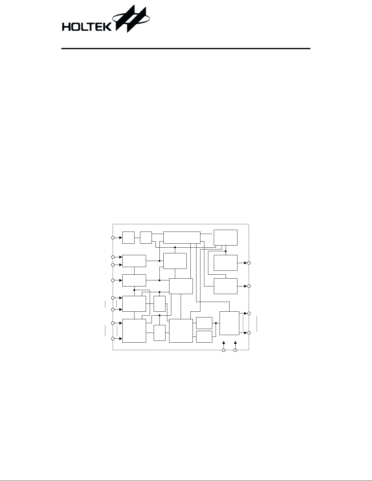
Block Diagram
OSC
ZIN 3
ZIN 0
XIN7
XIN0
TT1
TT2
MS
RC
OSC
Test
M ode
Mode
S e le c tio n
Z-key
Encoder
X-key
Encoder
PAL
PAL
P a r a lle l
To Serial
C onverter
Output
Stage
M odulation
Output
Stage
Key Scan
Driver
D ecoder
VSS
CODE
MCODE
DRS7
DRS0
VDD
1
3´2
Z-key
PAL
X-key
PAL
13
2 D iv id e r
Reset
Action
Generator
Control
Unit
C om m and
And
S yste m
C ode Latch
Z-DRS
X-D RS
1 April 19, 2000
HT6230
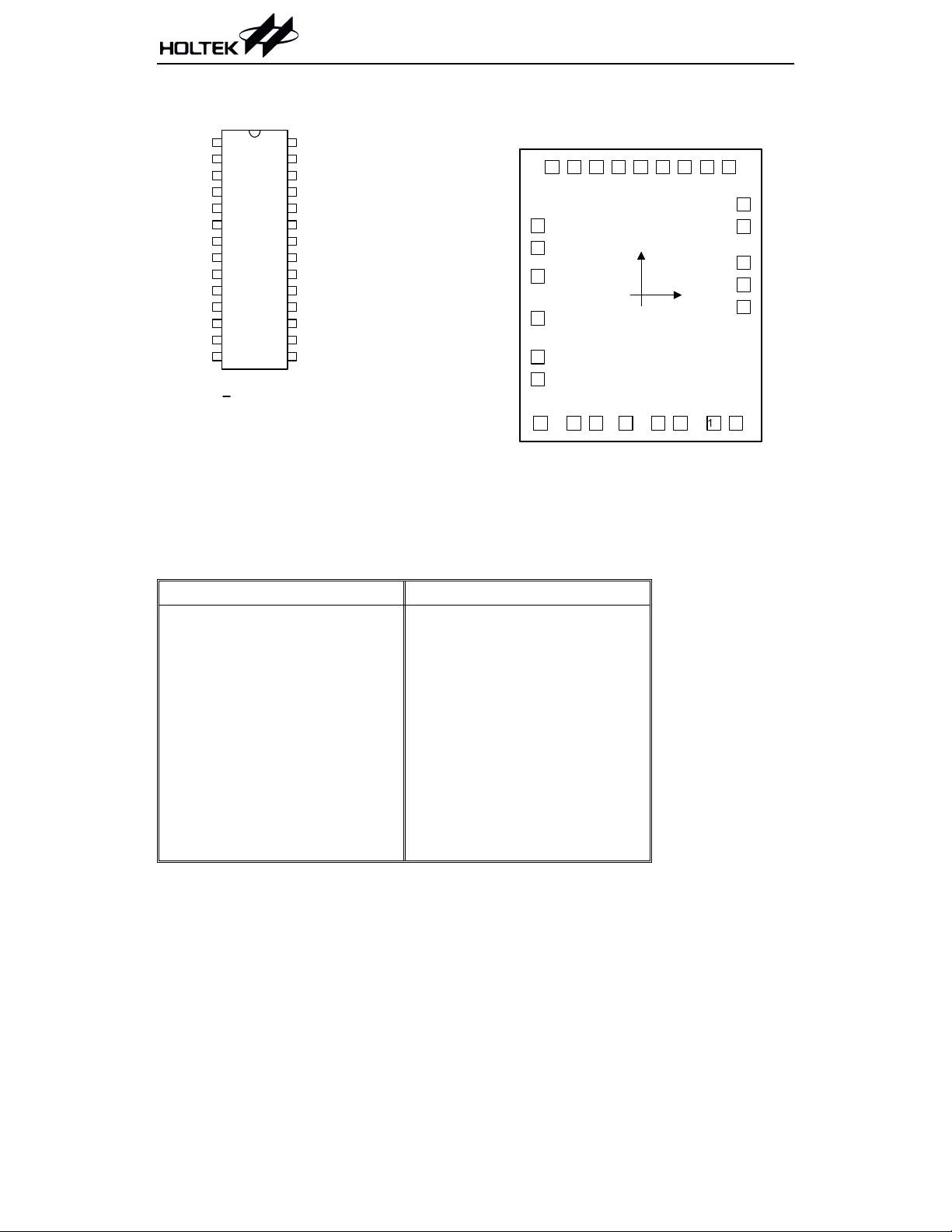
Pin Assignment Pad Assignment
ZIN 0
ZIN 1
MS
28
1
XIN 7
MS
ZIN 0
ZIN 1
ZIN 2
ZIN 3
MCODE
CODE
DRS7
DRS6
DRS5
DRS4
DRS3
VSS
2
3
4
5
6
7
8
9
10
11
12
13
14
H T 6230
2 8 S O P
VDD
27
XIN 6
26
XIN 5
25
XIN 4
24
XIN 3
23
XIN 2
22
XIN 1
21
XIN 0
20
TT1
19
TT2
18
OSC
17
DRS0
16
DRS1
15
DRS2
ZIN 2
ZIN 3
MCODE
CODE
DRS7
DRS6
DRS5
1
27
28
2
3
4
5
6
7
8
9
DRS4
102411
DRS3
Chip size: 1605 ´ 1910 (mm)
* The IC substrate should be connected to VDD in the
layout artwork.
XIN 7
XIN 5
XIN 6
VDD
25
(0 ,0 )
122613
VSS
DRS2
XIN 4
XIN 3
21
22
23
XIN 2
20
XIN 1
19
XIN 0
18
TT1
17
TT2
16
15
14
DRS1
DRS0
OSC
2
Pad Coordinates
Pad No. X Y Pad No. X Y
1
2
3
4
5
6
7
8
9
10
11
-570.19
-662.85
-662.85
-662.85
-662.85 -147.93
-662.85 -395.02
-662.85 -536.45
-644.16 -817.68
-429.58 -817.68
-288.15 -817.68
-98.77 -817.68
12 107.68
13 249.11
14 463.69
817.68 15 605.12
442.16 16 653.07
300.74 17 653.07 65.84
120.29 18 653.07 207.26
19 653.07 437.29
20 653.07 578.71
21 561.23 817.68
22 419.80 817.68
23 278.37 817.68
24 136.94 817.68
-817.68
-817.68
-817.68
25
26
27
28
-4.48
-145.91
-287.34
-428.76
2 April 19, 2000
Unit: mm
-817.68
-75.59
817.68
817.68
817.68
817.68
Pad Description
HT6230
Pad No. Pad Name I/O
1~3
28
ZIN1~ZIN3
ZIN0
4 MCODE O
5 CODE O
6~10 DRS7~DRS3 O
11 VSS
¾¾
12~14 DRS2~DRS0 O
I
Internal
Connection
CMOS with
PMOS Pull-high
Tri-state
CMOS
Tri-state
CMOS
Open Drain
NMOS
Open Drain
NMOS
Detect inputs from Z-key matrix
Generate modulation output data code with
1/12 system frequency and 1/4 duty cycle
Generates output data code
Drive for key scanning
Negative power supply, ground
Drive for key scanning
15 OSC I CMOS Oscillator input
Switch to four operating modes:
0 0 normal mode
16~17 TT2~TT1 I CMOS
0 1 test mode 1
1 0 test mode 2
1 1 Reset
18~24 XIN0~XIN6 I
25 VDD
26 XIN7 I
¾¾
CMOS with
PMOS Pull-high
CMOS with
PMOS Pull-high
Detect inputs from X-key matrix
Positive power supply
Detect input from X-key matrix
Select system mode (Two modes provided:
27 MS I CMOS
One-key system mode and Two-key system
mode)
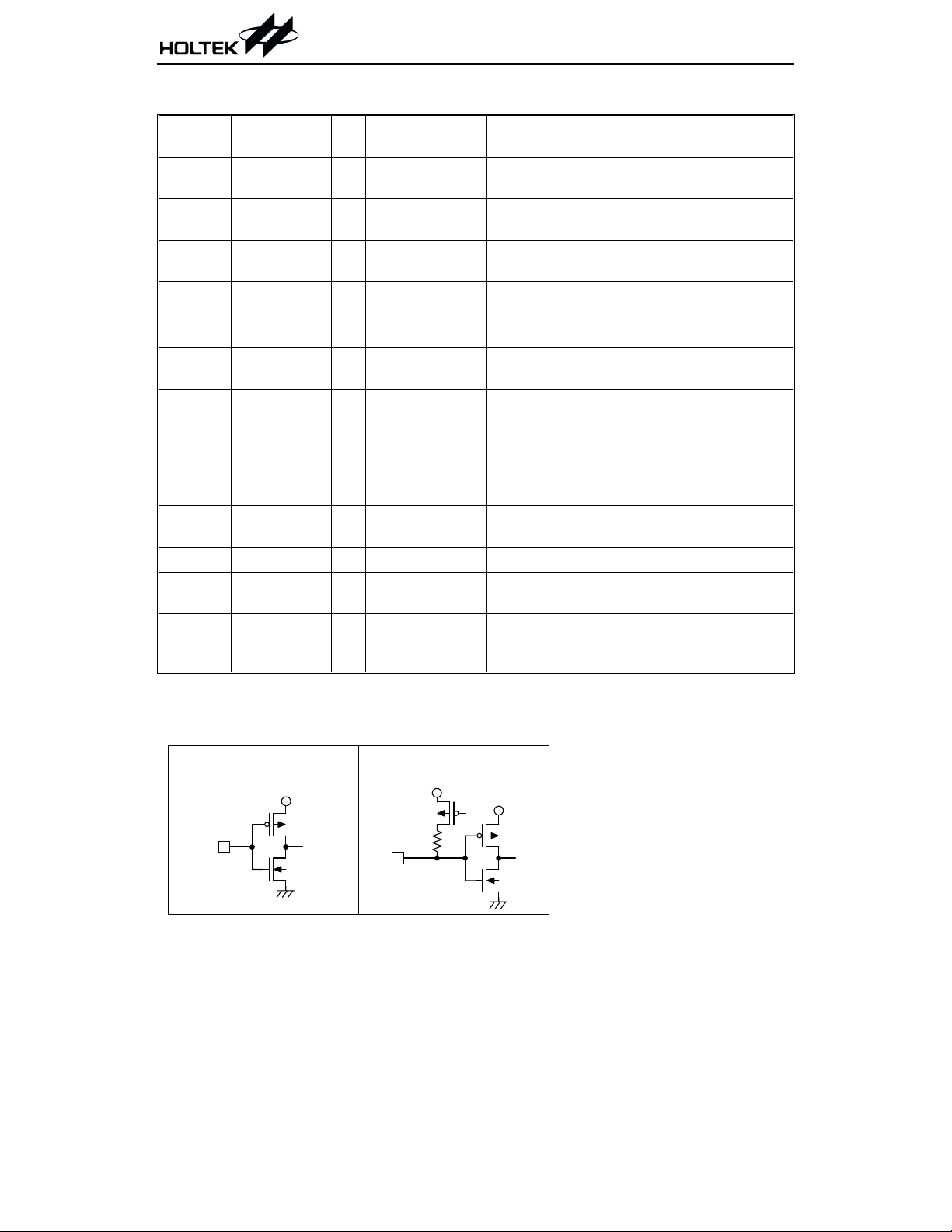
Description
Approximate internal connection circuits
·
Input terminal
P in : M S , T T 1 , T T 2 , O S C
V
DD
P in : X IN 0 ~ X IN 7 , Z IN 0 ~ Z IN 3
(w ith p u ll-h ig h re s is to r)
V
DD
V
DD
3 April 19, 2000

·
Output terminal
Pin: DRS0~DRS7 P in : C O D E , M C O D E
ENB
DATA IN
Absolute Maximum Ratings
HT6230
V
DD
Supply Voltage..............................-0.3V to 5.5V
Input Voltage .................V
-0.3V to VDD+0.3V
SS
Storage Temperature.................-50°Cto125°C
Operating Temperature ..............-25°Cto75°C
Note: These are stress ratings only. Stresses exceeding the range specified under ²Absolute Maxi
mum Ratings² may cause substantial damage to the device. Functional operation of this de
vice at other conditions beyond those listed in the specification is not implied and prolonged
exposure to extreme conditions may affect device reliability.
Electrical Characteristics
Ta=25°C
Test Conditions
Symbol Parameter
V
DD
V
OL1
V
OL2
V
OH
R
PH
Supply Voltage
DRS0~DRS7 Output
Voltage Low
CODE, MCODE Output
Voltage Low
CODE, MCODE Output
Voltage High
XIN0~XIN7 and
ZIN0~ZIN3 Pull-high
Oscillator Frequency
f
OSC
Operational
Free-running
V
DD
Conditions
¾¾
=0.3mA
I
3V
OL1
=0.6mA
I
3V
OL2
=-0.4mA VDD-0.3
I
3V
OH
TT1=TT2=MS=Low
3V
V
=0V
I
¾¾
3V
¾
Min. Typ. Max. Unit
2.4
¾¾
¾¾
¾
429
30
5.2 V
¾
0.3 V
0.3 V
¾¾
27
¾ kW
¾
V
kHz
50 100 kHz
-
-
4 April 19, 2000

Functional Description
Key operation
When MS is low, the legal key operation is that
only one ZIN or XIN can be connected to one
DRS driver and if more than one XIN, ZIN or
both are pressed at the same time then the key
operation is recognized as illegal; hence, the os
cillator will not start. When MS is high, the le
gal key operation is that exactly one ZIN and
one XIN are connected to two DRS drivers and
other cases of key operation are all considered
as illegal.
However, when one XIN or ZIN is connected to
more than one DRS, the last key scan driver is
to generate output data code.
Format of transmission code
The output pin CODE transmits the data code
as a code format, as shown at the bottom figure.
The method of transmitting one code bit is called
biphase transmission and is represented by the
following fig:
logic 0 logic 1
Where one code bit time is 3´2
put signal of the MCODE pin is the signal of the
generated output code modulated by 1/12 of the
system frequency with 1/4 duty cycle. In quies-
8
´T
. The out-
OSC
cent state both CODE and MCODE are high
impedance.
Key scan drivers
The key scan drivers DRS0 to DRS7 are open
drain NMOS and the outputs of these are all
low in quiescent state. When a legal key opera
tion is detected, the debounce cycle starts and
at the end of the debounce cycle, the DRS out
puts are high impedance. Furthermore, the
scanning cycle starts and DRS outputs take
turns to switch to low state.
Programmable output data code
The output data code corresponding to each key
is programmable by hardware mask option.
The PAL circuit is necessary for this purpose.
Operation mode
·
One-key system mode
The device enters this mode by switching the
MS input pin to low state. The pull-high resis
tors are connected to all XIN and ZIN inputs
so that all sense inputs are at high state, until
pulled to low state by key operation. In this
mode the legal key operation is that only one
ZIN or XIN can be connected to one DRS.
When a sense input detects a low level, an enable signal is generated to latch the system or
command latches. If the sense input belongs
to ZIN, the corresponding system code is generated and the command code is defined as all
HT6230
-
-
-
D ebounce cycle
(16 bit-tim e)
start
start
one code
11 LSB MSB LSB
Scan
cycle
C ode 1 C ode 2
16 bit-tim e
Start
bits
R epetition tim e (64 bit-tim e)
MSB
C ontrol
bit
48 bit-tim e 16 bit-tim e
5 system bits 6 co m m and bits
Transmission code format
5 April 19, 2000

HT6230
logic 1. If the sense input comes from XIN, the
corresponding command code together with
the system code stored in the system latches
are generated.
·
Two-key system mode
The device goes into this mode by switching
the MS input pin to high state. The pull-high
resistors are only connected to XIN inputs ex
cept the first scan cycle. In the first scan cycle,
there only exists pull-high resistors in ZIN in
puts. In this mode, the legal key operation is
that exactly one XIN and one ZIN are con
nected to two DRS drivers. In the first scan
duration, it detects which key in Z-key matrix
is pressed and generates an enable signal to
latch the system latches. While in the second
scan duration, it detects which key in the
X-key matrix is pressed and generates an en
abled signal to latch the command latches. Af
ter being latched, the system and command
codes are transmitted.
Control bit
A control bit is added after two start bits and
will be complemented if one key is released. The
decoder can decide whether the next code is a
new command or not.
·
During Tsep and debounce time, the device
will reset immediately if a key is released.
·
During Scan cycle in Tcode, a reset will occur
if a key is released in three cases described be
low:
¨
When one of the key scan drivers is in the
low state
-
-
-
¨
Before that key has been detected
¨
When MS is high and there is no wired con
nection in Z-key matrix
Test pins (TT1 and TT2)
There are four modes by the combination of TT1
and TT2.
TT1 TT2 Mode
-
-
0 0 Normal mode
1 1 Reset
1 0 Test mode 1
0 1 Test mode 2
-
-
Oscillator
The embedded part of the oscillator is an
RC-oscillation circuit. The OSC pin is the input
terminal of the RC-oscillation circuit and is connected to an external ceramic resonator (429kHz).
A resistor of 6.8kW must be in series with the
resonator. The resonator and resistor are
grounded at one side.
Reset (after key release)
In a complete code repetition time, as shown in
the figure below, the following situation of key
release results in a reset action.
C ode 1 C ode 2
Tcode
Tsep
R epetition tim e
D ebounce
tim e
Tcode
6 April 19, 2000

Application Circuits
V
DD
In fra -R e d
47
9
1k
9
10
11
12
13
14
1
XIN7
2
MS
3
ZIN 0
4
ZIN 1
5
ZIN 2
6
ZIN 3
7
MCODE
8
CODE
9
DRS7
DRS6
DRS5
DRS4
DRS3
VSS
DRS0
DRS1
DRS2
HT6230
2 8 S O P
VDD
XIN6
XIN5
XIN4
XIN3
XIN2
XIN1
XIN0
TT1
TT2
OSC
V
DD
28
27
26
25
24
23
22
21
20
19
18
17
16
15
R esonator (429kH z)
6 .8 k
HT6230
9
w here push-button sw itch
7 April 19, 2000

HT6230
Holtek Semiconductor Inc. (Headquarters)
No.3 Creation Rd. II, Science-based Industrial Park, Hsinchu, Taiwan, R.O.C.
Tel: 886-3-563-1999
Fax: 886-3-563-1189
Holtek Semiconductor Inc. (Taipei Office)
5F, No.576, Sec.7 Chung Hsiao E. Rd., Taipei, Taiwan, R.O.C.
Tel: 886-2-2782-9635
Fax: 886-2-2782-9636
Fax: 886-2-2782-7128 (International sales hotline)
Holtek Semiconductor (Hong Kong) Ltd.
RM.711, Tower 2, Cheung Sha Wan Plaza, 833 Cheung Sha Wan Rd., Kowloon, Hong Kong
Tel: 852-2-745-8288
Fax: 852-2-742-8657
Copyright Ó 2000 by HOLTEK SEMICONDUCTOR INC.
The information appearing in this Data Sheet is believed to be accurate at the time of publication. However, Holtek
assumes no responsibility arising from the use of the specifications described. The applications mentioned herein are
used solely for the purpose of illustration and Holtek makes no warranty or representation that such applications
will be suitable without further modification, nor recommends the use of its products for application that may pres
ent a risk to human life due to malfunction or otherwise. Holtek reserves the right to alter its products without prior
notification. For the most up-to-date information, please visit our web site at http://www.holtek.com.tw.
8 April 19, 2000
-
 Loading...