


Features
Operating voltage: 2.4V~12V
·
Low power and high noise immunity CMOS
·
technology
Low standby current
·
Capable of decoding 12 bits of information
·
Pair with Holtek¢s312series of encoders
·
8~12 address pins
·
0~4 data pins
·
Trinary address setting
·
Applications
Burglar alarm system
·
Smoke and fire alarm system
·
Garage door controllers
·
Car door controllers
·
General Description
The 312decoders are a series of CMOS LSIs for
remote control system applications. They are
paired with 3
operation a pair of encoder/decoder with the
same number of address and data format
should be selected (refer to the encoder/decoder
cross reference tables).
12
The 3
and data from its corredponding series of
encoders that are transmitted by a carrier using an RF or an IR transmission medium. Then
it compares the serial input information twice
continuously with its local address. If no errors
12
series of encoders. For proper
series of decoders receive serial address
12
3
Series of Decoders
Received data are checked two times
·
Built-in oscillator needs only 5% resistor
·
VT goes high during a valid transmission
·
Easy interface with an RF or an infrared
·
transmission medium
Minimal external components
·
Package information: refer to Selection
·
Table
Car alarm system
·
Security system
·
Cordless telephones
·
Other remote control systems
·
or unmatched codes are encountered, the input
data codes are decoded and transferred to the
output pins. The VT pin also goes high to indicate a valid transmission.
12
The 3
ing 12 bits of information that consists of N bits
of address and 12-N bits of data. To meet various applications they are arranged to provide a
number of data pins ranging from 0 to 4 and an
address pin ranging from 8 to 12. Thus, various
combinations of address/data number are
available in different packages.
series of decoders are capable of decod-
1 December 13, 1999
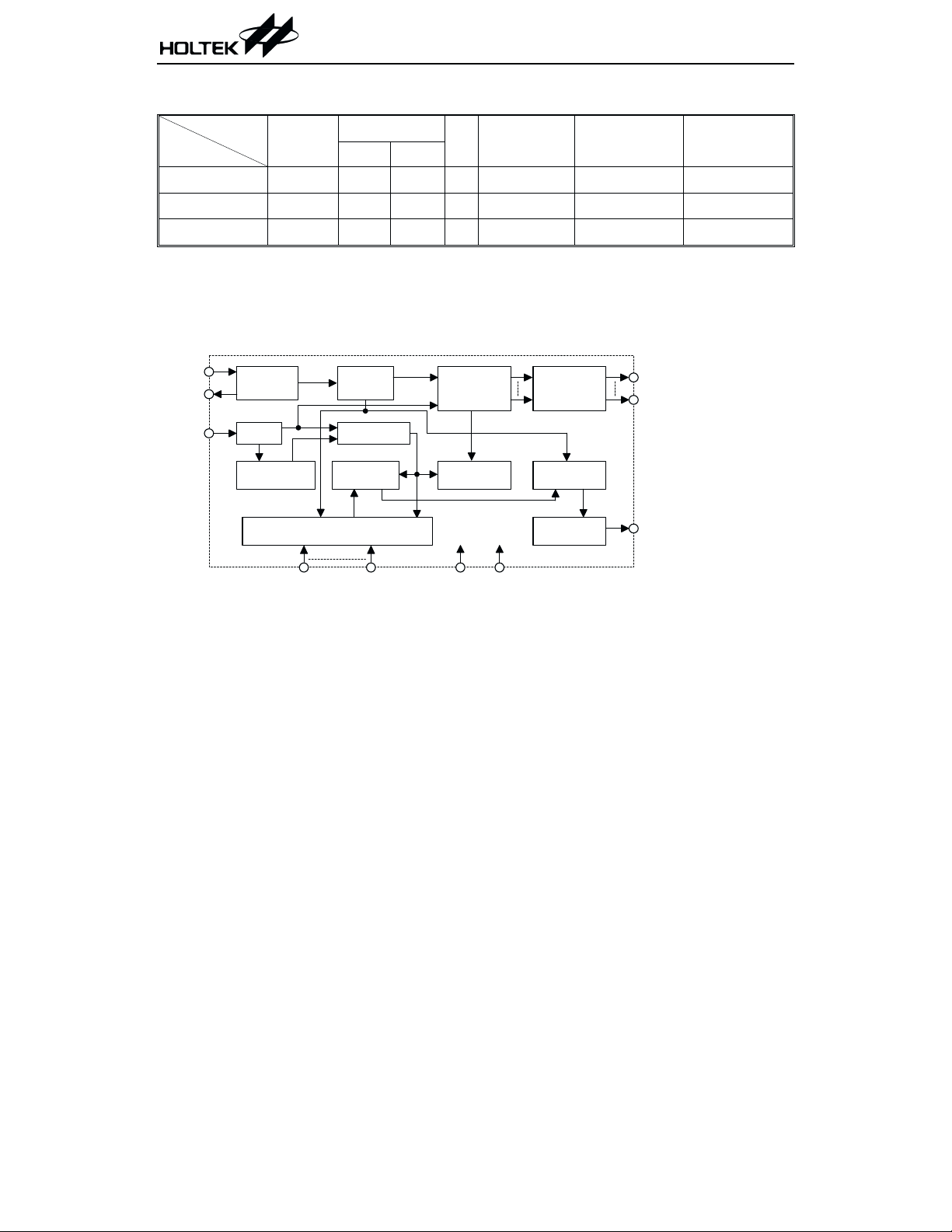
Selection Table
312Series of Decoders
Function
Part No. No. Type
Address
No.
HT6030 12 0
HT6032 10 2 L
HT6034 8 4 L
Data
¾Ö
VT Oscillator Trigger Package
RC oscillator
RC oscillator
Ö
RC oscillator
Ö
Note: Data type: L stands for latch type data output.
VT can be used as a momentary data output.
Block Diagram
OSC1
OSC2
DIN
O scillator
B u ffe r
Sync. D etector
D ivider
D a ta D e te c to r
C om parator Com parator
D a ta S h ift
R egister
DIN active ²Hi²
DIN active ²Hi²
DIN active ²Hi²
Latch C ircuit
C ontrol Logic
Buffer Tran sm ission G ate C ircuit
18 DIP/20 SOP
18 DIP/20 SOP
18 DIP/20 SOP
Data
VT
Address
VDD VSS
Note: The address/data pins are available in various combinations (refer to the address/data table).
2 December 13, 1999
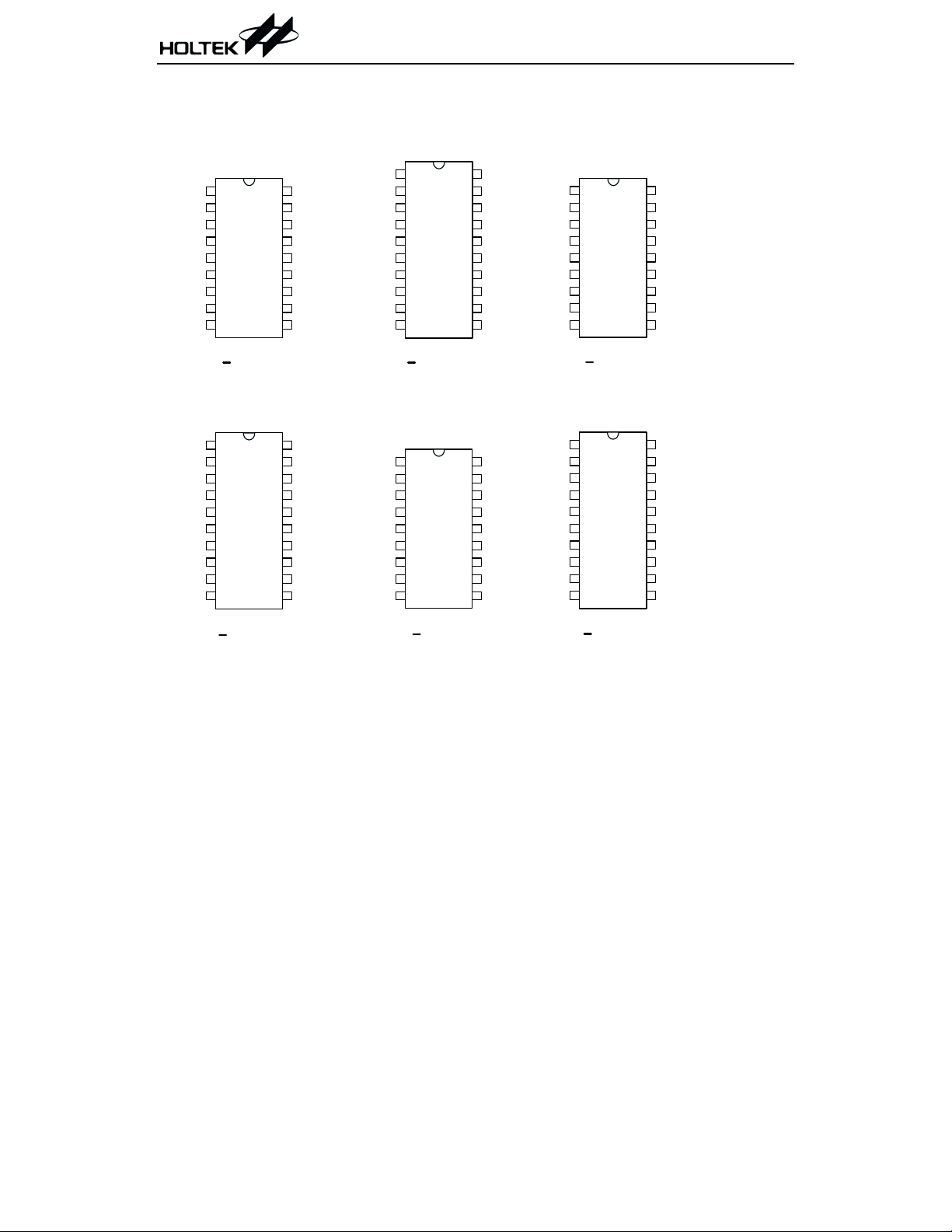
Pin Assignment
312Series of Decoders
12-A d dress
0 -D a ta
1
A0
2
A1
3
A2
4
A3
5
A4
6
A5
7
A6
8
A7
9
VSS
10-A d dress
2 -D a ta
NC
1
A0
2
A1
3
A2
4
A3
5
A4
6
A5
7
A6
8
A7
9
VSS
10
H T6032
H T6030
18 D IP
2 0 S O P
NC
VDD
VT
OSC2
OSC1
DIN
A11
A10
A9
A8
VDD
VT
OSC2
OSC1
DIN
D11
D10
D9
D8
10-A d dress
2 -D a ta
A0
1
A1
2
A2
3
A3
4
A4
5
A5
6
A6
7
A7
8
VSS
9
H T6032
8-A ddress
4-D ata
NC
1
A0
2
A1
3
A2
4
A3
5
A4
6
A5
7
A6
8
A7
9
VSS
10
H T6034
2 0 S O P
18 D IP
18
VDD
17
VT
16
OSC2
15
OSC1
14
DIN
13
D11
12
D10
11
A9
10
A8
20
NC
19
VDD
18
VT
17
OSC2
16
OSC1
15
DIN
14
D11
13
D10
12
D9
11
D8
12-A d dress
0 -D a ta
NC
18
VDD
17
VT
16
OSC2
15
OSC1
14
DIN
13
A11
12
A10
11
A9
10
A8
A0
A1
A2
A3
A4
A5
A6
A7
VSS
1
2
3
4
5
6
7
8
9
10
20
19
18
17
16
15
14
13
12
11
H T6030
2 0 S O P
8-A ddress
4-D ata
20
NC
19
VDD
18
VT
17
OSC2
16
OSC1
15
DIN
14
D11
13
D10
12
A9
11
A8
A0
A1
A2
A3
A4
A5
A6
A7
VSS
1
2
3
4
5
6
7
8
9
18
17
16
15
14
13
12
11
10
H T6034
18 D IP
3 December 13, 1999

Pin Description
312Series of Decoders
Pin Name I/O
A0~A11 I
Internal
Connection
TRANSMISSION
GATE
Description
Input pins for address A0~A11 setting
They can be externally set to VDD, VSS, or left open.
D8~D11 O CMOS OUT Output data pins
DIN I CMOS IN Serial data input pin
VT O CMOS OUT Valid transmission, active high
OSC1 I OSCILLATOR Oscillator input pin
OSC2 O OSCILLATOR Oscillator output pin
VSS
VDD
¾¾
¾¾
Negative power supply, ground
Positive power supply
Approximate internal connections
TRANSM ISSIO N
GATE
CMOS OUT
CMOS IN OSCILLATOR
OSC1
EN
OSC2
Absolute Maximum Ratings
Supply Voltage...............................-0.3V to 13V
Input Voltage....................V
-0.3 to VDD+0.3V
SS
Note: These are stress ratings only. Stresses exceeding the range specified under ²Absolute Maxi
mum Ratings² may cause substantial damage to the device. Functional operation of this device
at other conditions beyond those listed in the specification is not implied and prolonged expo
sure to extreme conditions may affect device reliability.
Storage Temperature.................-50°Cto125°C
Operating Temperature ..............-20°Cto75°C
4 December 13, 1999
-
-

312Series of Decoders
Electrical Characteristics
Symbol Parameter
V
I
STB
I
DD
I
O
I
VT
V
V
f
OSC
DD
IH
IL
Operating Voltage
Standby Current
Operating Current 5V
Data Output Source
Current (D8~D11)
Data Output Sink
Current (D8~D11)
VT Output Source Current
VT Output Source Current
Only For HT6033/35/45
VT Output Sink Current
VT Output Sink Current
Only For HT6033/35/45
²H² Input Voltage
²L² Input Voltage
Oscillator Frequency 5V
Test Conditions
V
DD
Conditions
¾¾
5V
Oscillator stops
12V
No load
f
=100kHz
OSC
=4.5V
V
5V
OH
=0.5V
V
5V
OL
V
=4.5V
OH
5V
V
=0.5V
OL
5V
5V
R
¾
¾
=91kW¾
OSC
Ta=25°C
Min. Typ. Max. Unit
2.4 5 12 V
¾
¾
¾
-0.5 -1 ¾
0.5 1
0.1 1
24
250 500
¾
mA
mA
mA
mA
mA
-2 -4 ¾
-0.35 -0.6 ¾
mA
12
0.35 0.6
3.5
0
¾
¾
100
¾
¾
5V
1V
kHz
¾
5 December 13, 1999

Functional Description
312Series of Decoders
Operation
12
The 3
binations of address and data pins in different
packages. They are paired with 3
series of decoders provide various com
12
series of
encoders. The decoders receive data transmit
ted by the encoders and interpret the first N
bits of the code period as addresses and the last
12-N bits as data (where N is the address code
number). A signal on the DIN pin then acti
vates the oscillator which in turn decodes the
incoming address and data. The decoders check
the received address twice continuously. If all
the received address codes match the contents
of the decoder¢s local address, the 12-N bits of
data are decoded to activate the output pins
and the VT pin is set high indicating a valid
transmission. That will last until the address
code is incorrect or no signal is received.
The output of the VT pin is high only when the
transmission is valid. Otherwise it is always low.
Output type
The data outputs follow the encoders during a
valid transmission and are then latched in
this state until the next valid transmission
occurs.
-
-
-
Flowchart
No
No
Power on
Standby m ode
A re
C ode in ?
Yes
Address bits
m atched ?
Yes
Store data
Match
previously stored
data ?
Yes
2 tim es
of checking
com pleted ?
Yes
Latch/M om entary
data to output &
activate V T
D isable V T &
ignore the rest of
th is w o rd
No
No
No
Address or
data error ?
Yes
The oscillator is disabled in the standby state
and activated as long as a logic ²high² signal is
applied to the DIN pin. i.e., the DIN pin should
be kept ²low² if there is no signal input.
6 December 13, 1999

Decoder timing
Encoder
Transm ission
Enable
Encoder
Data Out
D ecoder V T
M om entary
Data Out
Latched
Data Out
< 1 w ord
3 w ords 3 w ords
2 w ords
check
14
2 clo cks
1/2 clock period 1/2 clock period
Transm itted
C ontinuously
check
Encoder/Decoder cross reference tables
Part No. Data Pins Address Pins VT Pair Encoder
HT6030 0 12
Ö
HT6010 18, 20 20 18 20
HT6010 18, 20 20 18 20
HT6032 2 10
Ö
HT6012 18 20 18 20
HT6010 18, 20 20
HT6034 4 8
Ö
HT6014 18 20
312Series of Decoders
14
2 clo cks
Package
Encoder Decoder
DIP SOP DIP SOP
18 20
Address/Data sequence
The following table describes the position of the address/data sequence for various models of the 3
12
series of decoders. A correct device should be selected according to the requirements of individual address
and data.
Address/Data Bits
Part No.
0 1 2 3 4 5 6 7 8 9 10 11
HT6030 A0 A1 A2 A3 A4 A5 A6 A7 A8 A9 A10 A11
HT6032 A0 A1 A2 A3 A4 A5 A6 A7 A8 A9 D10 D11
HT6034 A0 A1 A2 A3 A4 A5 A6 A7 D8 D9 D10 D11
7 December 13, 1999

Oscillator frequency vs supply voltage
OSC
f
(S cale)
2.00
312Series of Decoders
OSC
R
(9)
1.75
1.50
1.25
(100kH z) 1.00
0.75
0.5
0.25
2.4 3 4 5 6 7 8
The recommended oscillator frequency is f
910111213
(decoder) @ 33 f
OSCD
OSCE
62k
91k
180k
270k
390k
560k
820k
2M
(encoder)
VDD (V D C )
8 December 13, 1999

Application Circuits
312Series of Decoders
R e c e iv e r C ir c u it
1
A0
2
A1
3
A2
4
A3
5
A4
6
A5
7
A6
8
A7
9
VSS
H T6030
VDD
VT
OSC2
OSC1
DIN
A11
A10
A9
A8
V
DD
18
17
16
R
OSC
15
14
13
12
11
10
R e c e iv e r C ir c u it
1
A0
2
A1
3
A2
4
A3
5
A4
6
A5
7
A6
8
A7
9
VSS
H T6034
Note: Typical infrared receiver: PIC-12043T/PIC-12043S (KODESHI CORP.)
or LTM9052 (LITEON CORP.)
Typical RF receiver: JR-200 (JUWA CORP.)
RE-99 (MING MICROSYSTEM, U.S.A.)
VDD
VT
OSC2
OSC1
DIN
D11
D10
D9
D8
V
DD
18
17
16
R
OSC
15
14
13
12
11
10
9 December 13, 1999

312Series of Decoders
Holtek Semiconductor Inc. (Headquarters)
No.3 Creation Rd. II, Science-based Industrial Park, Hsinchu, Taiwan, R.O.C.
Tel: 886-3-563-1999
Fax: 886-3-563-1189
Holtek Semiconductor Inc. (Taipei Office)
5F, No.576, Sec.7 Chung Hsiao E. Rd., Taipei, Taiwan, R.O.C.
Tel: 886-2-2782-9635
Fax: 886-2-2782-9636
Fax: 886-2-2782-7128 (International sales hotline)
Holtek Semiconductor (Hong Kong) Ltd.
RM.711, Tower 2, Cheung Sha Wan Plaza, 833 Cheung Sha Wan Rd., Kowloon, Hong Kong
Tel: 852-2-745-8288
Fax: 852-2-742-8657
Copyright Ó 1999 by HOLTEK SEMICONDUCTOR INC.
The information appearing in this Data Sheet is believed to be accurate at the time of publication. However, Holtek
assumes no responsibility arising from the use of the specifications described. The applications mentioned herein are
used solely for the purpose of illustration and Holtek makes no warranty or representation that such applications
will be suitable without further modification, nor recommends the use of its products for application that may pres
ent a risk to human life due to malfunction or otherwise. Holtek reserves the right to alter its products without prior
notification. For the most up-to-date information, please visit our web site at http://www.holtek.com.tw.
10 December 13, 1999
-
 Loading...