

HT— 2050 DEC.29.199 3
FIVE LAMP/LED FLASH DRIVER PAGE: 1
A. General Description —
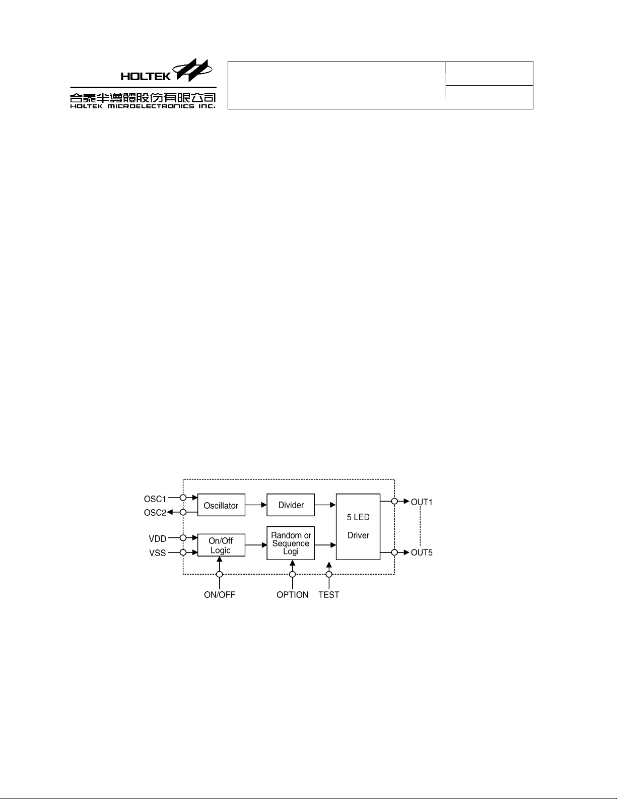
The HT–2050 is a low cost, low-power C-MOS LSI designed for lamp and
LED flash driver. It has five flash outputs with 10mA drive capability that can
implement random or sequence flashing function controlled by one option pin.
It only requires one external resistor for typical application. It is very suitable
for the use of the flash products such as disco glasses, disco hat, gift card,
X’mas decoration and so forth.
B. Features —
• C-MOS Metal-Gate Process.
• Operating voltage: 1.2V ~ 4.5V.
• Low stand-by current: 1µA at 3V.
• Five lamp flash driver with 10mA driving capability.
• Random or sequence flash selection
• toggle on/off control function.
• 1/10 duty cycle output.
• Built-in oscillator.
• Minimum external components.
C. Block Diagram —
HT— 2050 DEC.29.199 3
FIVE LAMP/LED FLASH DRIVER PAGE: 2
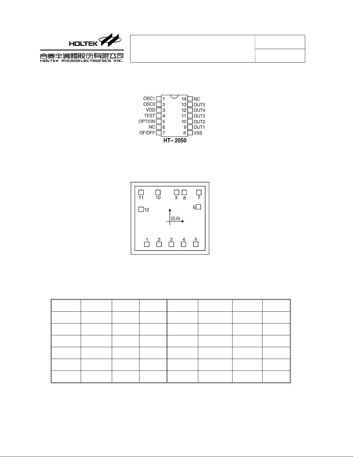
D. Pin Assignment —
E. Pad Assignme nt & Position —
Chip Size: 64 × 59 (mil)
* The IC substrate should be connected to VDD in PCB layout artwork.
Pad No. Symbol x Y Pad No. Symbol X Y
1 OUT1 –21.09 –20.9 7 OSC2 26.55 26.5
2 OUT2 –9.89 –20.9 8 VDD 13.35 26.5
3 OUT3 1.31 –20.9 9 TEST 6.15 26.5
4 OUT4 12.51 –20.9 10 OPT –10.89 26.5
5 OUT5 23.71 –20.9 11 ON/OFF –26.25 26.5
6 OSC1 26.23 13.3 12 VSS –26.25 10.98
2
Unit: mil

HT— 2050 DEC.29.199 3
FIVE LAMP/LED FLASH DRIVER PAGE: 3
F. Absolute Maximum Ratings —
Parameter Symbol Minimum Maximum Unit
Supply Voltage V
Input/Output Voltage V
Storage Temperature T
Operating Temperature T
G. Electrical Characteristics —
Symbol Parameter
V
I
F
STB
I
I
OSC
Operating Voltage — — 1.2 3 4.5 V
DD
Stand-by Current 3V — — 1 2
Operating Current 3V No load — 200 500
DD
Output Sink Current
OL
Oscillator Frequency —
DD
I, VO
STG
OP
–0.3 5 V
VSS–0.3 VDD+0.3 V
–50 125
070
°C
°C
Test Condition
Min. Typ. Max. Unit
V
DD
1.5V V
Condition
=0.5V 5 8 — mA
OL
3V VOL=0.5V 10 15 — mA
R=150K~300KΩ
—64K— Hz
µA
µΑ

HT— 2050 DEC.29.199 3
FIVE LAMP/LED FLASH DRIVER PAGE: 4
H. Pad Description —
Pad No. Pad Name I/O Description
1 OUT1 O Lamp/LED flash drive output pad.
2 OUT2 O Lamp/LED flash drive output pad.
3 OUT3 O Lamp/LED flash drive output pad.
4 OUT4 O Lamp/LED flash drive output pad.
5 OUT5 O Lamp/LED flash drive output pad.
6 OSC1 I Oscillator input pad.
7 OSC2 O Oscillator output pad.
8 VDD I Positive power supply.
9 TEST I/O For IC test only.
10 OPTION I Random or sequence function selection pad.
11 ON/OFF I Togale ON/OFF control pad.
12 VSS I Negative power supply, GND.
Note:
OPTION= 1
OPTION= Open
→ Sequence Mode
→ Random Mode

I. Application Diagram —
HT— 2050 DEC.29.199 3
FIVE LAMP/LED FLASH DRIVER PAGE: 5
 Loading...