

HT93214 Series
1-memory Tone/Pulse Dialer
Features
·
Operating Voltage: 2.0V~5.5V
·
Low standby current
·
Low memory retention current: 0.1mA (Typ.)
·
Tone/Pulse switchable
·
32 (pulse)/31 (tone) digits for redialing
·
Pause and P ® T key for PBX
·
4´4 keyboard matrix
·
3.58MHz crystal or ceramic resonator
·
Hand-free control
Patent Number: 86474, 84545(R.O.C)
·
Pause, P ® T can be saved for redialing
·
One-key redialing
·
Keytone output
·
Pause time: 2.2s
·
Cascadable manual dialing after redialing
·
Calibrated DTMF timing for redialing
·
HT93214A: 16-pin DIP/NSOP package
HT93214B/AT: 18-pin DIP package
General Description
The HT93214 are dialer series designed for low cost
telephone set applications with expandable features
such as Lock function, keytone and LCD display interface. With a 4´4 keyboard, it performs normal
tone/pulse switchable dialing, and provides one-key
redialing function with a 32-digit memory for speed dial-
ing. An on-chip oscillator is built-in to work with an external 3.58Mhz crystal or ceramic resonator for accurate
timing. The HT93214 provides 300ms (F1 key) and
600ms (F2 key) of flash time; Tone dialing and 10pps,
20pps selection with 1/2 M/B ratio for pulse dialing.
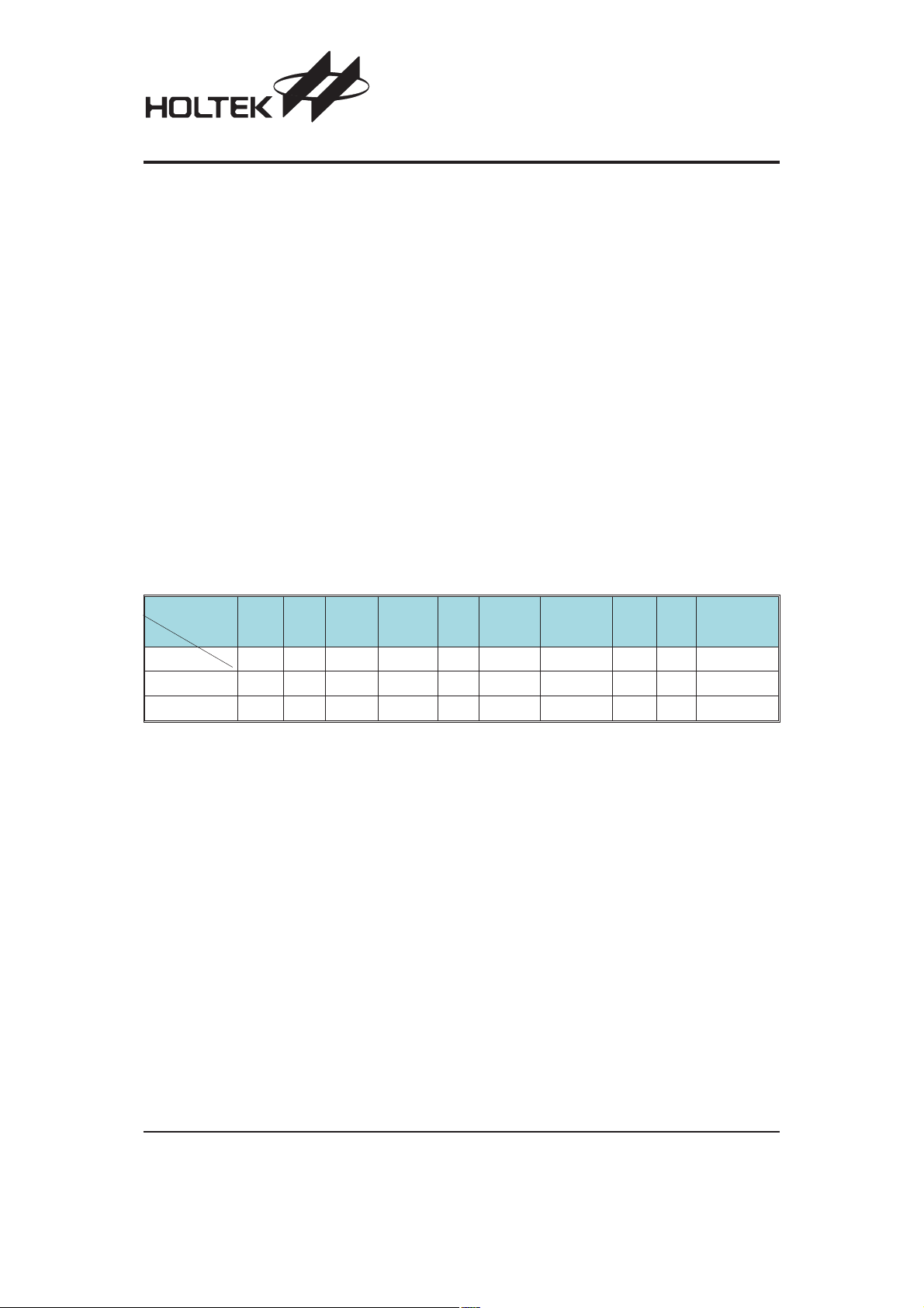
Selection Table
Function
Part No.
HT93214A Control 300/600 N 94 96 10/20 1/2 16DIP/NSOP
HT93214B
HT93214AT
Hand-
Free
Ö
Key
Flash
Tone
Control 300/600 N 94 96 10/20 1/2 18DIP
Control 300/600 N 94 96 10/20 1/2 18DIP
Ö
Flash
Time
(ms)
Pulse
No.
Tone
Duration
(ms)
Inter Tone
Pause (ms)
PPS M/B Package
Rev. 1.20 1 October 7, 2010
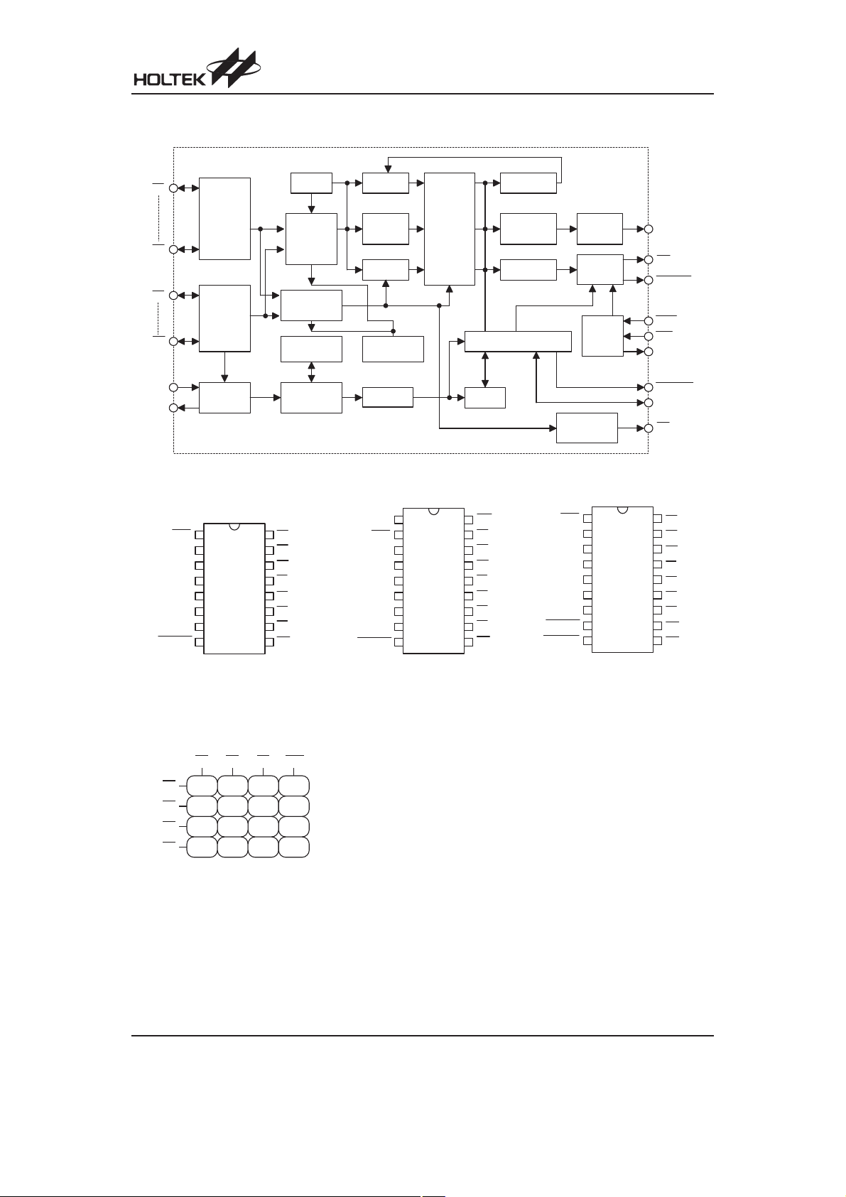
Block Diagram
1 6
1 5
1 4
1 3
1 2
1 1
1 0
9
1
2
3
4
5
6
7
8
1 8
1 7
1 6
1 5
1 4
1 3
1 2
1 1
1 0
1
2
3
4
5
6
7
8
9
H K S
M O D E
X 1
X 2
V S S
V D D
D T M F
X M U T E
R 4
R 3
R 2
R 1
C 3
C 2
C 1
P O
H F O
H K S
M O D E
X 1
X 2
V S S
V D D
D T M F
X M U T E
1 8
1 7
1 6
1 5
1 4
1 3
1 2
1 1
1 0
1
2
3
4
5
6
7
8
9
H K S
M O D E
X 1
X 2
V S S
V D D
D T M F
X M U T E
M O D E O
R 4
R 3
R 2
R 1
C 3
C 2
C 1
P O
K T
H T 9 3 2 1 4 A
1 6 D I P - A / N S O P - A
H T 9 3 2 1 4 B
1 8 D I P - A
H T 9 3 2 1 4 A T
1 8 D I P - A
H F I
R 4
R 3
R 2
R 1
C 3
C 2
C 1
P O
C 1
R 1
P O
K e y
C o l u m n
F S M
K e y
F u n c t i o n
E n c o d e r
E n c o d e r
C o n t r o l
W R M
C o u n t e r
A D D R L
K e y R o w
S R A M
D e b o u n c e
D i v i d e r
C l o c k
G e n e r a t o r
M / B
F l a s h / M o d e
T i m e r
C h e c k
T o n e
E n c o d e r
C o n v e r t e r
H F
T o n e
O u t
P u l s e
O u t
X 1
X 2
D T M F
H F I
M O D E
M O D E O
X M U T E
C 3
R 4
C l o c k
C o n t r o l
K e y t o n e
G e n e r a t o r
H K S
H F O
K T
2
5
8
0
3
6
9
#
F 1
F 2
P
R
C 1 C 2 C 3
R 4
R 3
R 2
R 1
1
4
7
* / T
H K S
Pin Assignment
HT93214 Series
Keyboard Information
Rev. 1.20 2 October 7, 2010
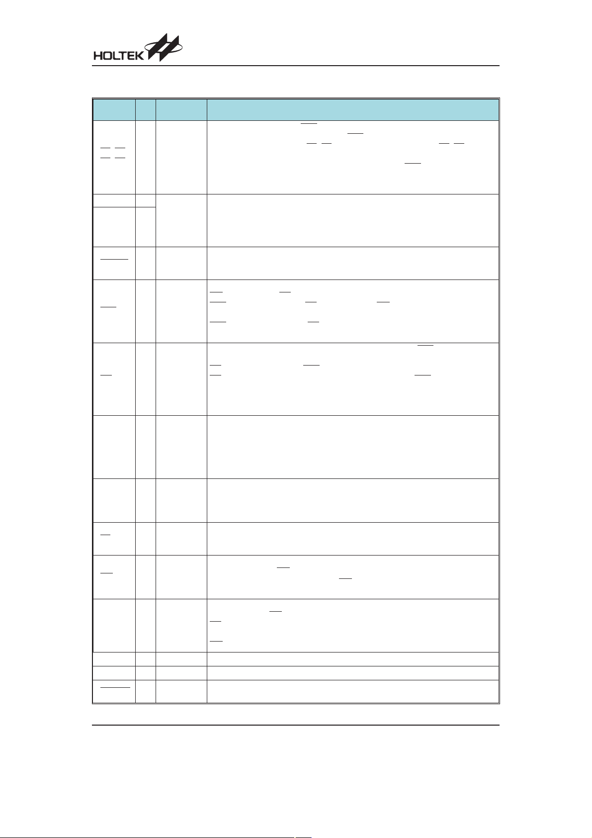
Pin Description
Pin Name I/O
~C3
C1
R1~R4
X1 I
X2 O
XMUTE
HKS
PO
MODE I/O CMOS
DTMF O CMOS
KT
HFI
HFO O CMOS
VDD
VSS
MODEO
Internal
Connection
I/O
O
Open Drain
I CMOS
O NMOS
O NMOS
I CMOS
¾¾
¾¾
O NMOS
CMOS
I/O
OSC
NMOS
HT93214 Series
Description
These pins along with the HKS
board input detection. When on-hook (HKS
off-hook the column group (C1
high for input detection.
Pressing a key connects a single row to a single column HKS
tem oscillator that results in a dialing signal output. If more than two keys are
pressed at the same time, no response occurs. The key-in debounce time is 20ms.
The system oscillator consists of an inverter, a bias resistor and the necessary load
capacitor on chip. Connecting a standard 3.579545MHz crystal or ceramic resonator to the X1 and X2 terminals can implement the oscillator function. The oscillator is
turned off in the standby mode, and is actuated whenever a keyboard entry is detected.
NMOS open drain structure pulled to VSS during dialing signal transmission. Otherwise, it is an open circuit. This pin is used to mute the speech circuit when transmitting the dial signal.
This pin is used to monitor the status of the hook-switch and its combination with
can control the PO pin output to make or break the line.
HFI
HKS
=VDD: On-hook state (PO=low). Except for HFI (hand-free control input), other
functions are all disabled.
HKS
=VSS: Off-hook state (PO=high). The chip is in the stand-by mode and ready
to receive the key input.
NMOS open drain output structure, which by receiving the HKS
control the dialer so as to connect or disconnect the telephone line.
PO
is pulled to VSS when HKS is high (on-hook) and HFO is low.
PO
is an open circuit which make the line connection when HKS is low (off-hook) or
HFO is high.
During the off-hook state, this pin also outputs the dialing pulse train in pulse mode
dialing. While in the tone mode, this pin is always an open circuit.
This is a tri-state input/output pin, used for dialing mode selection, either Tone
mode or Pulse mode, 10pps/20pps
MODE=VDD: Pulse, 10pps, M/B=1/2
MODE=Floating: Pulse, 20pps, M/B=1/2
MODE=VSS: Tone.
The MODE selection is checked each time a key input is received.
This pin is active only when the chip transmits tone dialing signals. Otherwise, it always outputs a low. The pin outputs tone signals to drive the external transmitter
amplifier circuit. The load resistor (to V
load connected to V
NMOS open drain structure for keytone output. It outputs 34ms of 600Hz tone burst
when any key is pressed in the pulse mode or when a function key is pressed in the
tone mode.
Pulled-high, this pin is a Schmitt trigger input structure. Active low. Applying a negative going pulse to HFI
function. The pull-high resistance of HFI
work is recommended for input debouncing.
The HFO pin is a CMOS output structure. Its output is toggle- controlled by a negative transition on HFI
PO
outputs a high to connect the line.
The hand-free function can be released by an on-off-hook operation or by another
HFI
input. Refer to the functional description for the hand-free functional operation.
Positive power supply, 2.0V~5.5V for normal operation
Negative power supply, ground
NMOS open drain output pin pulled to VSS during tone output and is an open circuit
during pulse output.
DD
pin. When HFO is high, the hand-free function is enabled and
form a 4´4 keyboard matrix which can perform key
=high) all the pins are set high. While
~C3) is set low and the row group (R1~R4) remains
and actuates the sys
and HFO signals,
) should not be less than 5kW and any DC
is not allowed.
can toggle the HFO once and hence control the hand-free
SS
is about 200kW typ. An external RC net-
-
-
Rev. 1.20 3 October 7, 2010
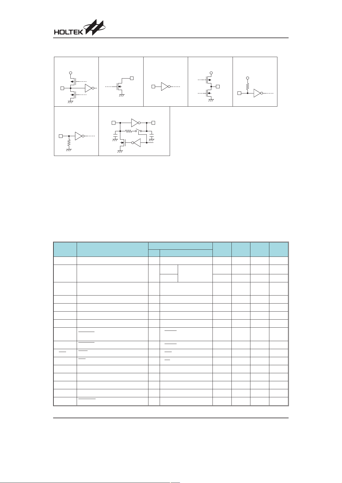
Approximate internal connection circuits
N M O S O U T
V
D D
C M O S I N / O U T C M O S O U T
C M O S I N
P u l l - L o w
C M O S I N
P u l l - H i g h
C M O S I N
O S C I L L A T O R
X 1
X 2
E N
1 0 M
2 0 P
1 0 P
V
D D
Absolute Maximum Ratings
Supply Voltage ............................................-0.3V to 6V
Input Voltage..............................V
-0.3V to VDD+0.3V
SS
HT93214 Series
Storage Temperature ............................-50°Cto125°C
Operating Temperature...........................-20°Cto75°C
Note: These are stress ratings only. Stresses exceeding the range specified under ²Absolute Maximum Ratings² may
cause substantial damage to the device. Functional operation of this device at other conditions beyond those
listed in the specification is not implied and prolonged exposure to extreme conditions may affect device reliability.
Electrical Characteristics
Symbol Parameter
V
DD
I
DD
I
STB
V
R
I
R
V
IL
V
IH
I
XMO
I
OLXM
I
HKS
R
HFI
I
OH1
I
OL1
I
OH2
I
OL2
I
OL3
Operating Voltage
Operating Current 2.5V
Standby Current 1V
Memory Retention Voltage
Memory Retention Current 1V On-hook
Input Low Voltage
Input High Voltage
XMUTE Leakage Voltage
XMUTE Sink Current 2.5V
HKS Pin Input Current 2.5V
HFI Pull- High Resistance 2.5V
Keypad Pin Source Current 2.5V
Keypad Pin Sink Current 2.5V
HFO Pin Source Current 2.5V
HFO Pin Sink Current 2.5V
MODEO Sink Current 2.5V
V
DD
¾¾
¾¾
¾¾
¾¾
¾
Test Conditions
Conditions
Pulse
Off-hook
Keypad entry
Tone
On-hook, no load
No entry
=12V
V
XMUTE
No entry
V
=0.5V
XMUTE
V
=2.5V
HKS
V
=0V
HFI
V
=0V
OH
V
=2.5V
OL
V
=2V
OH
V
=0.5V
OL
V
=0.5V
OL
F
=3.5795MHz, Ta=25°C
OSC
Min. Typ. Max. Unit
2
¾
¾
¾
0.2 1 mA
0.6 2 mA
¾¾
V
0.8V
1
¾
SS
DD
¾
0.1 0.2
¾
¾
¾¾
1
¾¾
¾
¾
200
5.5 V
1
5V
0.2V
DD
V
DD
1
0.1
¾ kW
-4 ¾-40 mA
200 400
¾mA
-1 ¾¾
1
0.6 3.5
¾¾
¾
mA
mA
V
V
mA
mA
mA
mA
mA
mA
Rev. 1.20 4 October 7, 2010
HT93214 Series
Symbol Parameter
T
T
F
T
T
T
FP
RP
OSC
DB
BRK
HKDL
Pause Time After Flash 2.5V
One-key Redialing Pause Time 2.5V
System Frequency
Key-in Debounce Time 2.5V
Break TimeFor One-key Redialing 2.5V
Off-hook Delay Time 2.5V
V
Pulse Mode Electrical Characteristics
Symbol Parameter
I
POH
I
POL
P
PO Output Source Current 2.5V
PO Output Sink Current 2.5V
Pulse Rate
R
M/B Make/Break Ratio
T
T
T
T
T
Pre-digit-pause Time
PDP
Inter-digit-pause Time
IDP
Pulse Make Duration
M
Pulse Break Duration
B
Pause Time
P
V
Test Conditions
DD
Conditions
¾¾
¾¾
¾¾ ¾
Min. Typ. Max. Unit
800
800
3.58
¾¾20¾
¾¾
10pps
20pps
Test Conditions
V
OH
V
OL
Conditions
=2V
=0.5V
DD
MODE pin is
connected to V
¾
MODE pin is opened
DD
¾
¾
Min. Typ. Max. Unit
-0.2 ¾¾
0.2 0.6
¾
¾
¾¾ ¾
M/B=33:66 (10 pps)
¾
M/B=33:66 (20 pps)
10 pps
¾
20 pps
10 pps, M/B=1/2
¾
20 pps, M/B=1/2
10 pps, M/B=1/2
¾
20 pps, M/B=1/2
¾
¾
¾
¾
¾
¾
¾
¾
¾¾ ¾
2.2
800
500
F
=3.5795MHz, Ta=25°C
OSC
10
20
33:66
33
17
800
500
33.3
16.7
66.6
33.3
2.2
¾
¾
¾
ms
ms
MHz
ms
¾
¾
¾
s
ms
mA
¾
¾
mA
pps
¾
¾
¾
¾
¾
¾
¾
¾
¾
¾
¾
%
ms
ms
ms
ms
s
Tone Mode Electrical Characteristics
Symbol Parameter
V
I
V
R
A
TDC
TOL
TAC
L
CR
DTMF Output DC Level
DTMF Sink Current 2.5V
DTMF Output AC Level
DTMF Output Load 2.5V
Column Pre-emphasis 2.5V Row group=0dB 1 2 3 dB
THD Tone Signal Distortion 2.5V
T
TMIN
T
ITPM
THD (Distortion) (dB) = 20 log (
Minimum Tone Duration
Minimum Inter-Tone Pause
22 2
V1 V2 .... Vn
+++/Vi Vh
V
Test Conditions
DD
¾
¾
Conditions
No load
V
=0.5V
DTMF
Row group,
=5kW
R
L
0.45V
THD£-23dB
=5kW¾-30 -23
R
L
Auto-redial
¾
Auto-redial
¾
22
)
+
F
=3.5795MHz, Ta=25°C
OSC
Min. Typ. Max. Unit
0.1
¾
DD
¾¾
0.7V
DD
V
mA
0.12 0.155 0.18 Vrms
5
¾¾kW
dB
¾
¾
94
96
¾
¾
ms
ms
Vi, Vh: Row group and column group signals
V1, V2, ... Vn: Harmonic signals (BW=300Hz~3500Hz)
Rev. 1.20 5 October 7, 2010
Functional Description
Keyboard matrix
C1
~C3, HKS and R1~R4 form a keyboard matrix. To
gether with a standard 4´4 keyboard, the keyboard
matrix is used for dialing entries. The keyboard ar
rangement of the HT93214 series is shown in the Key
board Information.
Tone frequency
Tone
Name
R1
R2
R3
R4
C1
C2
C3
Note: % Error does not contain the crystal frequency
Dialing specification selection
·
The specifications are selected by the MODE pin.
MODE Tone/Pulse Dial Rate M/B Ratio
VDD Pulse 10pps 1/2
VSS Tone
Floating Pulse 20pps 1/2
·
The MODE pin status is checked whenever a digit key
is pressed, however the M/B and pulse rate are determined at the first key entry.
Hand-free function operation
·
When HFO is low, a falling edge triggers the HFI,enabling the Hand-free function (HFO becomes high).
·
Reset Hand-free function
When HFO is high, the Hand-free function is enabled
and can be reset by:
¨
Off-hook
¨
Applying a falling edge to HFI
·
Hand-free function table
Current State Next State
Hook SW HFO Input HFO Dialing?
On-hook High
Off-hook High
On-hook
Off-hook Low on-hook Low No
Off-hook High on-hook High Yes
Output Frequency (Hz)
Specified Actual
697 699 +0.29%
770 766
852 847
941 948 +0.74%
1209 1215 +0.50%
1336 1332
1477 1472
drift
¾
Low
¾
¯
HFI
HFI
¯
HFI
¯
of
off-hook
% Error
-0.52%
-0.59%
-0.30%
-0.34%
¾¾
High Yes
Low No
Low Yes
Low Yes
HT93214 Series
Flash
Two flash keys are provided, namely F1, F2 for both se
ries. All the flash key function as control key with differ
ent break duration. Whenever a flash key is pressed the
-
pin will be forced low for a TFduration and the trans
PO
-
mission of the new digit key inputs will be further de
layed for a T
duration selection.
HT93214 300ms 600ms
Key definition
·
0,1,2,3,4,5,6,7,8,9 keys
These are dialing number input keys for both the
pulse mode and the tone mode operation.
·
*/T
This key executes the P®T function and waits a T
duration in the pulse mode. On the other hand, the */T
key executes the * function in the tone mode. The */T
key will occupy one memory digit in either tone or
pulse mode.
·
#
This is a dialing signal key for the tone mode only, no
response in the pulse mode.
·
F1, F2
Pressing one of the flash keys will force the PO
become low for the T
signals of the key input that are entered after the F
key, a wait period T
low is provided.
·
P
Pause key. The execution of this key pauses the output for the T
·
R
Redial key. It executes redialing as well as one-key redial function.
after TF. See the following table for flash
FP
Item F1 F2
duration. To transmit the dial
F
(sec) after PO pin returns from
FP
duration (2.2s).
P
-
-
-
-
P®T
pin to
Rev. 1.20 6 October 7, 2010
HT93214 Series
K e y b o a r d i n p u t : D 1 D 2 . . . D n
-
P u l s e m o d e
( a ) w i t h o u t * / T
D i a l i n g o u t p u t : D 1 D 2 . . . D n
R M : D 1 D 2 . . . D n
( b ) w i t h * / T
D i a l i n g o u t p u t : D 1 D 2 . . . D n T
P ® T
D n + 1 . . . D m
R M : D 1 D 2 . . . D n * / T D n + 1 . . . D m
T o n e
P u l s e
·
N o r m a l d i a l i n g
K e y b o a r d i n p u t : D 1 D 2 . . . D n * / T D n + 1 . . .
D m
( a ) w i t h o u t * / T
D i a l i n g o u t p u t : D 1 D 2 . . . D n
R M : D 1 D 2 . . . D n
( b ) w i t h * / T
D i a l i n g o u t p u t : D 1 D 2 . . . D n * D n + 1 . . . D m
R M : D 1 D 2 . . . D n * D n + 1 . . . D m
-
T o n e m o d e
( a ) w i t h o u t * / T
D i a l i n g o u t p u t : D 1 D 2 . . . D n
R M : U n c h a n g e d
R M c o n t e n t : D 1 D 2 . . . D n
( b ) w i t h * / T
D i a l i n g o u t p u t : D 1 D 2 . . . D n T
P ® T
D n + 1 . . . D m
R M : U n c h a n g e d
R M c o n t e n t : D 1 D 2 . . . D n * / T D n + 1 . . . D m
D i a l i n g o u t p u t : D 1 D 2 . . . D n
R M : U n c h a n g e d
R M c o n t e n t : D 1 D 2 . . . D n
( b ) w i t h * / T
D i a l i n g o u t p u t : D 1 D 2 . . . D n * D n + 1 . . . D m
R M : U n c h a n g e d
R M c o n t e n t : D 1 D 2 . . . D n * / T D n + 1 . . . D m
-
P u l s e m o d e
-
T o n e m o d e
P u l s e
T o n e
·
R e d i a l
K e y b o a r d i n p u t : D 1 D 2 . . . D n * / T D n + 1 . . .
D m
( a ) w i t h o u t * / T
K e y b o a r d i n p u t : D 1 D 2 . . . D n
K e y b o a r d i n p u t : R
K e y b o a r d i n p u t : R
K e y b o a r d i n p u t : R
K e y b o a r d i n p u t : R
N o t e : T h e m a x i m u m c a p a c i t y o f t h e R M m e m o r y i s 3 2 d i g i t s . W h e n m o r e t h a n 3 2 d i g i t s a r e e n t e r e d ,
t h e s i g n a l i s t r a n s m i t t e d b u t t h e r e d i a l f u n c t i o n i s i n h i b i t e d .
Keyboard Operation
The followingoperations are described under an on-off- hook oron-hook condition with the hand-free active condition.
Rev. 1.20 7 October 7, 2010

HT93214 Series
D m R
K e y b o a r d i n p u t : D 1 D 2 . . . D n * / T D n + 1 . . .
K e y b o a r d i n p u t : D 1 D 2 . . . D n R
( a ) w i t h o u t * / T
D i a l i n g o u t p u t : D 1 D 2 . . . D n T
B R K
T
R P
R M : D 1 D 2 . . . D n
( b ) w i t h * / T
R M : D 1 D 2 . . . D n * / T D n + 1 . . . D m
( a ) w i t h o u t * / T
R M : D 1 D 2 . . . D n
( b ) w i t h * / T
-
T o n e m o d e
-
P u l s e m o d e
P u l s e
T
B R K
T
R P
D 1 D 2 . . . D n T
P®T
P u l s e
D i a l i n g o u t p u t : D 1 D 2 . . . D n * D n + 1 . . . D m
R M : D 1 D 2 . . . D n * D n + 1 . . . D m
T
B R K
T
R P
D 1 D 2 . . . D n * D n + 1
. . . D m
T o n e
D i a l i n g o u t p u t : D 1 D 2 . . . D n T
P
®
T
D n + 1 . . . D m
T o n e
·
O n e - k e y r e d i a l
D 1 D 2 . . . D n
D i a l i n g o u t p u t : D 1 D 2 . . . D n T
B R K
T
R P
D 1 D 2
. . . D n
D n + 1 . . . D m
K e y b o a r d i n p u t : D 1 D 2 . . . D n R
D m R
K e y b o a r d i n p u t : D 1 D 2 . . . D n * / T D n + 1 . . .
N o t e : I f t h e d i a l i n g n u m b e r e x c e e d s 3 2 d i g i t s , r e d i a l i n g i s i n h i b i t e d a n d P O = o p e n
-
F l a s h a s a c o n t r o l k e y
·
F l a s h
R M : D n + 1 . . . D m
D i a l i n g o u t p u t : D 1 D 2 . . . D n T
F
T
F P
D n + 1 . . .
D m
N o t e : T
F
: b r e a k a f l a s h t i m e
K e y b o a r d i n p u t : D 1 D 2 . . . D n F D n + 1 . . .
D m
D i a l i n g o u t p u t : D 1 D 2 . . . D n TP D n + 1 . . . D m
R M : D 1 D 2 . . . D n P D n + 1 . . . D m
·
P a u s e
K e y b o a r d i n p u t : D 1 D 2 . . . D n P D n + 1 . . . D m
·
N o t e
R M : R e d i a l m e m o r y
D 1 D 2 . . . D n : 0 ~ 9
D n + 1 . . . D m : 0 ~ 9 ,
*
, #
Rev. 1.20 8 October 7, 2010

Timing Diagrams
H K S
K E Y I N
T
D B
T
P D P
T
M
T
M
T
B
T
I D P
- T
M
T
P D P
T
I D P
H i g h I m p e d a n c e
X M U T E
R
D 2D 1
T
D B
T
M
T
I D P
- T
M
T
D B
D T M F
K T
X 2
T
K T
T
K T
T
K T
T
I D P
- T
M
2 0 m s 2 0 m s
P O
6 0 0 H z c a r r i e r
T
I D P
- T
M
X 2
D T M F
H i g h I m p e d a n c e
T
D B
T
I T P M
T
I T P M
T
T M I N
K E Y I N
RD 1
T
I T P M
T
I T P M
K T
T
D B
T
D B
D 2
H K S
X M U T E
2 0 m s 2 0 m s
P O
M O D E O
Normal dialing
·
Pulse mode
HT93214 Series
·
Tone mode
Rev. 1.20 9 October 7, 2010

Dialing with PAUSE key
K E Y I N
X 2
T
I D P
T
D B
H i g h I m p e d a n c e
D 3
D 2D 1
T
M
T
M
TP + T
P D P
P
T
I D P
- T
M
D T M F
K T
T
K T
T
K T
P O
H K S
X M U T E
T
P D P
2 0 m s
T
I D P
- T
M
T
I D P
- T
M
6 0 0 H z c a r r i e r
X 2
D T M F
H i g h I m p e d a n c e
T
D B
T
I T P M
K E Y I N
D 3D 2
T
T M I N
T
I T P M
P
T
P
T
I T P M
D 1
K T
H K S
X M U T E
2 0 m s
P O
M O D E O
·
Pulse mode
HT93214 Series
·
Tone mode
Rev. 1.20 10 October 7, 2010

·
K E Y I N
X 2
T
F P
T
F
H i g h I m p e d a n c e
T
D B
2 0 m s
D T M F
K T
T
K T
H K S
X M U T E
F
P O
6 0 0 H z c a r r i e r
1 . 2 k H z c a r r i e r
K E Y I N
X 2
D T M F
H i g h I m p e d a n c e
T
P D P
T
I D P
+ T
P D P
T
D B
T
I T P M
T
I D P
T
P®T
D 1
2 0 m s
D 2
D 3
* / T
K T
T
K T
H K S
X M U T E
P O
T
T M I N
6 0 0 H z c a r r i e r
M O D E O
Flash key operation
·
Pulse to Tone operation
HT93214 Series
Rev. 1.20 11 October 7, 2010

·
T
R P
T
B R K
T
I T P M
T
I T P M
H i g h I m p e d a n c e
T
I T P M
T
I T P M
K E Y I N
X 2
D T M F
D 1 D 2 R
K T
T
D B
T
D B
T
D B
H K S
X M U T E
2 0 m s
P O
T
K T
M O D E O
One key redial operation
HT93214 Series
Rev. 1.20 12 October 7, 2010

Application Circuits
X M U T E
R 1
R 2
R 3
R 4
P O H K S
H T 9 3 2 1 4 S e r i e s
V S S M O D E X 1 X 2
V D D
M / B = 2 / 3
M / B = 1 / 2
T o n e
3 . 5 8 M H z
r e s o n a t o r
V D D
1 5 0
W
5 . 1 V
1 N 4 1 4 8
A 4 2
A 9 2
2 2 M
W
T i p
R i n g 1 A b r i d g e
2
5
8
0
1
4
7
* / T
3
6
9
#
F 1
F 2
P
R
1 0 p F
V D D
1 N 4 1 4 8
O f f - h o o k
O n - h o o k
H F O
D T M F
S P E E C H
N E T W O R K
1
m
F
H A N D - F R E E
N E T W O R K
H F O
V D D
M O D E O
V D D
H F I K T
C 1C 2
C 3
* U n s p e c i f i e d t r a n s i s t o r s a r e o f 8 0 5 0 t y p e
* A m F c a p a c i t o r b e t w e e n X M U T E a n d V S S ( G N D ) i s r e c o m m e n d e d
3 9 p F 3 9 p F
1 . 5 k
W
1 0 0 k
W
2 2 0 k
W
1
m
F
1 0 0
m
F
2 7 0 k
W
0 . 1
m
F
2 . 2 k
W
1 0 0 k
W
1 0 0 k
W
3 . 3 k
W
4 7 k
W
HT93214 Series
Rev. 1.20 13 October 7, 2010

Package Information
1 6
1
9
8
A
B
C
D
E
F
G
H
I
1 6
1
9
8
A
B
C
D
E
F
G
H
I
16-pin DIP (300mil) Outline Dimensions
HT93214 Series
Fig1. Full Lead Packages
·
MS-001d (see fig1)
Symbol
A 0.780
B 0.240
C 0.115
D 0.115
E 0.014
F 0.045
G
H 0.300
I
Symbol
A 19.81
B 6.10
C 2.92
D 2.92
E 0.36
F 1.14
G
H 7.62
I
Fig2. 1/2 Lead Packages
Dimensions in inch
Min. Nom. Max.
¾
¾
¾
¾
¾
¾
¾
0.100
¾
¾¾
0.880
0.280
0.195
0.150
0.022
0.070
¾
0.325
0.430
Dimensions in mm
Min. Nom. Max.
¾
¾
¾
¾
¾
¾
¾
2.54
¾
¾¾
22.35
7.11
4.95
3.81
0.56
1.78
¾
8.26
10.92
Rev. 1.20 14 October 7, 2010

·
MS-001d (see fig2)
Symbol
A 0.735
B 0.240
C 0.115
D 0.115
E 0.014
F 0.045
G
H 0.300
I
HT93214 Series
Dimensions in inch
Min. Nom. Max.
¾
¾
¾
¾
¾
¾
¾
¾¾
0.100
¾
0.775
0.280
0.195
0.150
0.022
0.070
¾
0.325
0.430
Symbol
A 18.67
B 6.10
C 2.92
D 2.92
E 0.36
F 1.14
G
H 7.62
I
Dimensions in mm
Min. Nom. Max.
¾
¾
¾
¾
¾
¾
¾
¾¾
2.54
¾
19.69
7.11
4.95
3.81
0.56
1.78
¾
8.26
10.92
Rev. 1.20 15 October 7, 2010

·
MO-095a (see fig2)
Symbol
A 0.745
B 0.275
C 0.120
D 0.110
E 0.014
F 0.045
G
H 0.300
I
HT93214 Series
Dimensions in inch
Min. Nom. Max.
¾
¾
¾
¾
¾
¾
¾
¾¾
0.100
¾
0.785
0.295
0.150
0.150
0.022
0.060
¾
0.325
0.430
Symbol
A 18.92
B 6.99
C 3.05
D 2.79
E 0.36
F 1.14
G
H 7.62
I
Dimensions in mm
Min. Nom. Max.
¾
¾
¾
¾
¾
¾
¾
¾¾
2.54
¾
19.94
7.49
3.81
3.81
0.56
1.52
¾
8.26
10.92
Rev. 1.20 16 October 7, 2010

16-pin NSOP (150mil) Outline Dimensions
1 6
1
9
8
a
A
B
C
D
E
F
G
H
C '
·
MS-012
Symbol
Min. Nom. Max.
A 0.228
B 0.150
C 0.012
C¢
D
E
0.386
¾¾
¾
F 0.004
G 0.016
H 0.007
a 0°¾8°
Dimensions in inch
¾
¾
¾
¾
0.050
¾
¾
¾
HT93214 Series
0.244
0.157
0.020
0.402
0.069
¾
0.010
0.050
0.010
Symbol
A 5.79
B 3.81
C 0.30
C¢
D
E
F 0.10
G 0.41
H 0.18
Min. Nom. Max.
9.80
¾¾
¾
Dimensions in mm
¾
¾
¾
¾
1.27
¾
¾
¾
6.20
3.99
0.51
10.21
1.75
¾
0.25
1.27
0.25
a 0°¾8°
Rev. 1.20 17 October 7, 2010

18-pin DIP (300mil) Outline Dimensions
1 8
1
1 0
9
A
B
C
D
E
F
G
H
I
1 8
1
1 0
9
A
B
C
D
E
F
G
H
I
HT93214 Series
Fig1. Full Lead Packages
·
MS-001d (see fig1)
Symbol
A 0.880
B 0.240
C 0.115
D 0.115
E 0.014
F 0.045
G
H 0.300
I
Symbol
A 22.35
B 6.10
C 2.92
D 2.92
E 0.36
F 1.14
G
H 7.62
I
Fig2. 1/2 Lead Packages
Dimensions in inch
Min. Nom. Max.
¾
¾
¾
¾
¾
¾
¾
0.100
¾
¾
0.430
0.920
0.280
0.195
0.150
0.022
0.070
¾
0.325
¾
Dimensions in mm
Min. Nom. Max.
¾
¾
¾
¾
¾
¾
¾
2.54
¾
¾
10.92
23.37
7.11
4.95
3.81
0.56
1.78
¾
8.26
¾
Rev. 1.20 18 October 7, 2010

·
MS-001d (see fig2)
Symbol
A 0.845
B 0.240
C 0.115
D 0.115
E 0.014
F 0.045
G
H 0.300
I
HT93214 Series
Dimensions in inch
Min. Nom. Max.
¾
¾
¾
¾
¾
¾
¾
¾
0.100
¾
0.430
0.880
0.280
0.195
0.150
0.022
0.070
¾
0.325
¾
Symbol
A 21.46
B 6.10
C 2.92
D 2.92
E 0.36
F 1.14
G
H 7.62
I
Dimensions in mm
Min. Nom. Max.
¾
¾
¾
¾
¾
¾
¾
¾
2.54
¾
10.92
22.35
7.11
4.95
3.81
0.56
1.78
¾
8.26
¾
Rev. 1.20 19 October 7, 2010

·
MO-095a (see fig2)
Symbol
A 0.845
B 0.275
C 0.120
D 0.110
E 0.014
F 0.045
G
H 0.300
I
HT93214 Series
Dimensions in inch
Min. Nom. Max.
¾
¾
¾
¾
¾
¾
¾
¾
0.100
¾
0.430
0.885
0.295
0.150
0.150
0.022
0.060
¾
0.325
¾
Symbol
A 21.46
B 6.99
C 3.05
D 2.79
E 0.36
F 1.14
G
H 7.62
I
Dimensions in mm
Min. Nom. Max.
¾
¾
¾
¾
¾
¾
¾
¾
2.54
¾
10.92
22.48
7.49
3.81
3.81
0.56
1.52
¾
8.26
¾
Rev. 1.20 20 October 7, 2010

Product Tape and Reel Specifications
A
C
B
T 1
T 2
D
Reel Dimensions
HT93214 Series
SOP 16N (150mil)
Symbol Description Dimensions in mm
A Reel Outer Diameter
B Reel Inner Diameter
C Spindle Hole Diameter
D Key Slit Width
T1 Space Between Flange
T2 Reel Thickness
330.0±1.0
100.0±1.5
13.0
2.0±0.5
16.8
22.2±0.2
+0.5/-0.2
+0.3/-0.2
Rev. 1.20 21 October 7, 2010

Carrier Tape Dimensions
PD 1
W
P 1P 0
D
E
F
t
K 0
B 0
A 0
C
I C p a c k a g e p i n 1 a n d t h e r e e l h o l e s
a r e l o c a t e d o n t h e s a m e s i d e .
R e e l H o l e
SOP 16N (150mil)
Symbol Description Dimensions in mm
W Carrier Tape Width
P Cavity Pitch
E Perforation Position
F Cavity to Perforation (Width Direction)
D Perforation Diameter 1.55
D1 Cavity Hole Diameter 1.50
P0 Perforation Pitch
P1 Cavity to Perforation (Length Direction)
A0 Cavity Length
B0 Cavity Width
K0 Cavity Depth
t Carrier Tape Thickness
C Cover Tape Width
16.0±0.3
8.0±0.1
1.75±0.1
7.5±0.1
+0.10/-0.00
+0.25/-0.00
4.0±0.1
2.0±0.1
6.5±0.1
10.3±0.1
2.1±0.1
0.30±0.05
13.3±0.1
HT93214 Series
Rev. 1.20 22 October 7, 2010

HT93214 Series
Holtek Semiconductor Inc. (Headquarters)
No.3, Creation Rd. II, Science Park, Hsinchu, Taiwan
Tel: 886-3-563-1999
Fax: 886-3-563-1189
http://www.holtek.com.tw
Holtek Semiconductor Inc. (Taipei Sales Office)
4F-2, No. 3-2, YuanQu St., Nankang Software Park, Taipei 115, Taiwan
Tel: 886-2-2655-7070
Fax: 886-2-2655-7373
Fax: 886-2-2655-7383 (International sales hotline)
Holtek Semiconductor Inc. (Shenzhen Sales Office)
5F, Unit A, Productivity Building, No.5 Gaoxin M 2nd Road, Nanshan District, Shenzhen, China 518057
Tel: 86-755-8616-9908, 86-755-8616-9308
Fax: 86-755-8616-9722
Holtek Semiconductor (USA), Inc. (North America Sales Office)
46729 Fremont Blvd., Fremont, CA 94538
Tel: 1-510-252-9880
Fax: 1-510-252-9885
http://www.holtek.com
Copyright Ó 2010 by HOLTEK SEMICONDUCTOR INC.
The information appearing in this Data Sheet is believed to be accurate at the time of publication. However, Holtek as
sumes no responsibility arising from the use of the specifications described. The applications mentioned herein are used
solely for the purpose of illustration and Holtek makes no warranty or representation that such applications will be suitable
without further modification, nor recommends the use of its products for application that may present a risk to human life
due to malfunction or otherwise. Holtek¢s products are not authorized for use as critical components in life support devices
or systems. Holtek reserves the right to alter its products without prior notification. For the most up-to-date information,
please visit our web site at http://www.holtek.com.tw.
-
Rev. 1.20 23 October 7, 2010
 Loading...