


HT46R32/HT46R34
A/D Type 8-Bit OTP MCU with OPA
Technical Document
·
Tools Information
·
FAQs
·
Application Note
-
HA0003E Communicating between the HT48 & HT46 Series MCUs and the HT93LC46 EEPROM
-
HA0049E Read and Write Control of the HT1380
-
HA0051E Li Battery Charger Demo Board - Using the HT46R47
-
HA0052E Microcontroller Application - Battery Charger
-
HA0083E Li Battery Charger Demo Board - Using the HT46R46
Features
·
Operating voltage:
f
=4MHz: 2.2V~5.5V
SYS
f
=8MHz: 3.3V~5.5V
SYS
·
20 bidirectional I/O lines (max.)
·
Single interrupt input shared with an I/O line
·
8-bit programmable timer/event counter with overflow
interrupt and 7-stage prescaler
·
Integrated crystal and RC oscillator
·
Watchdog Timer
·
2048´14 Program Memory capacity - HT46R32
4096´15 Program Memory capacity - HT46R34
·
88´8 Data Memory capacity - HT46R32
192´8 Data Memory capacity - HT46R34
·
Integrated PFD function for sound generation
·
Power-down and wake-up functions reduce power
consumption
·
Up to 0.5ms instruction cycle with 8MHz system clock
at V
=5V
DD
·
6-level subroutine nesting
·
4 channel 12-bit resolution A/D converter
·
Integrated single operational amplifier or comparator
selectable via configuration option
·
Dual 8-bit PWM outputs shared with I/O lines
·
Bit manipulation instruction
·
Full table read instruction
·
63 powerful instructions
·
All instructions executed in one or two machine
cycles
·
Low voltage reset function
·
28-pin SKDIP/SOP/SSOP package
General Description
-
The HT46R32 and HT46R34 are 8-bit, high perfor
mance, RISC architecture microcontroller devices. With
their fully integrated A/D converter they are especially
suitable for applications which interface to analog sig
nals, such as those from sensors. The addition of an in
ternal operational amplifier/comparator and PWM
modulation functions further adds to the analog capabil
ity of these devices.
Rev. 1.10 1 March 16, 2007
With the comprehensive features of low power con
sumption, I/O flexibility, programmable frequency di
vider, timer functions, oscillator options, multi-channel
-
A/D Converter OP/Comparator, Pulse Width Modula
-
tion function, Power-down and wake-up functions etc,
the application scope of these devices is broad and en
-
compasses areas such as sensor signal processing,
motor driving, industrial control, consumer products,
subsystem controllers, etc.
-
-
-
-
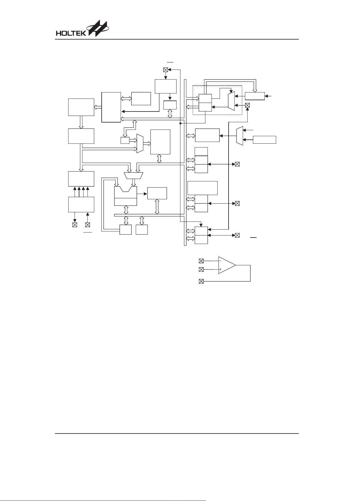
Block Diagram
P r o g r a m
R O M
I n s t r u c t i o n
R e g i s t e r
I n s t r u c t i o n
D e c o d e r
T i m i n g
G e n e r a t o r
P r o g r a m
C o u n t e r
M P
A L U
S h i f t e r
M U X
S T A C K
M
U
X
D A T A
M e m o r y
S T A T U S
P A 5 / I N T
I n t e r r u p t
C i r c u i t
I N T C
P A 3 , P A 5
T M R C
T M R
P A 3 / P F D
W D T
P W M
P D C
P D
4 - C h a n n e l
A / D C o n v e r t e r
P B C
P B
P o r t D
P o r t B
HT46R32/HT46R34
P r e s c a l e r f
U
X
P A 4
M
U
X
P D 0 / P W M 0
P D 1 / P W M 1
P D 2
P D 3
P B 0 / A N 0 ~ P B 3 / A N 3
P B 4 ~ P B 7
P A 4 / T M R
f
S Y S
W D T O S C
S Y SM
/ 4
O S C 2 O S C 1
R E S
V D D
V S S
L V RA C C
A P N
A P P
A P O
P A C
P o r t A
P A
P A 0 ~ P A 2
P A 3 / P F D
P A 4 / T M R
P A 5 / I N T
P A 6 ~ P A 7
Rev. 1.10 2 March 16, 2007
Pin Assignment
HT46R32/HT46R34
P B 5
1
P B 4
2
P A 3 / P F D
P B 3 / A N 3
P B 2 / A N 2
P B 1 / A N 1
P B 0 / A N 0
3
P A 2
4
P A 1
5
P A 0
6
7
8
9
1 0
A P O
1 1
A P N
1 2
A P P
1 3
V S S
1 4
H T 4 6 R 3 2 / H T 4 6 R 3 4
2 8 S K D I P - A / S O P - A / S S O P - A
2 8
2 7
2 6
2 5
2 4
2 3
2 2
2 1
2 0
1 9
1 8
1 7
1 6
1 5
P B 6
P B 7
P A 4 / T M R
P A 5 / I N T
P A 6
P A 7
O S C 2
O S C 1
V D D
R E S
P D 0 / P W M 0
P D 1 / P W M 1
P D 2
P D 3
Pin Description
Pin Name I/O Options Description
PA0~PA2
PA3/PFD
PA4/TMR
PA5/INT
PA6, PA7
PB0/AN0
PB1/AN1
PB2/AN2
PB3/AN3
PB4~PB7
PD0/PWM0
PD1/PWM1
PD2
PD3
APO
APN
APP
RES
VDD
VSS
OSC1
OSC2
I/O
Wake-up
PA3 or PFD
I/O Pull-high
Pull-high
Pull-high
I/O
PD0 or PWM0
PD1 or PWM1
O
I
¾
I
I
¾
¾¾
¾¾
I
O
Crystal
or RC
Bidirectional 8-bit input/output port. Each pin can be configured as wake-up
input by configuration options. Software instructions determine if the pin is a
CMOS output or Schmitt trigger input. Configuration options determine which
pins on the port have pull-high resistors. The PFD, TMR and INT
pin-shared with PA3, PA4 and PA5, respectively.
Bidirectional 8-bit input/output port. Software instructions determine if the
pin is a CMOS output or Schmitt trigger input. Configuration options determine
which pins on the port have pull-high resistors. Pins PB0~PB3 are pin-shared
with the A/D input pins. The A/D inputs are selected via software instructions.
Once selected as an A/D input, the I/O function and pull-high resistor are disabled automatically.
Bi-directional 4-bit input/output port. Software instructions determine if the
pin is a CMOS output or Schmitt trigger input. Configuration options determine
which pins on this port have pull-high resistors. PD0/PD1 are pin-shared with
the PWM0/PWM1 outputs selected via configuration option.
APO, APN and APP are the internal operational amplifier, output pin, nega
tive input pin and positive input pin respectively .
Schmitt trigger reset input. Active low.
Positive power supply
Negative power supply, ground.
OSC1, OSC2 are connected to an external RC network or external crystal,
determined by configuration option, for the internal system clock. If the RC
system clock option is selected, pin OSC2 can be used to measure the sys
tem clock at 1/4 frequency.
pins are
-
-
Rev. 1.10 3 March 16, 2007
HT46R32/HT46R34
Absolute Maximum Ratings
Supply Voltage...........................VSS-0.3V to VSS+6.0V
Input Voltage..............................V
Total ..............................................................150mA
I
OL
-0.3V to VDD+0.3V
SS
Total Power Dissipation .....................................500mW
Note: These are stress ratings only. Stresses exceeding the range specified under ²Absolute Maximum Ratings² may
cause substantial damage to the device. Functional operation of this device at other conditions beyond those listed
in the specification is not implied and prolonged exposure to extreme conditions may affect device reliability.
Storage Temperature ............................-50°Cto125°C
Operating Temperature...........................-40°Cto85°C
Total............................................................-100mA
I
OH
D.C. Characteristics
Symbol Parameter
V
DD
I
DD1
I
DD2
I
DD3
I
STB1
I
STB2
V
IL1
V
IH1
V
IL2
V
IH2
V
LVR
I
OL
I
OH
R
PH
V
AD
I
ADC
DNL ADC Differential Non-Linearity 5V
INL ADC Integral Non-Linearity 5V
RESOLU Resolution
Operating Voltage
Operating Current
(Crystal OSC)
Operating Current
(RC OSC)
Operating Current
(Crystal OSC, RC OSC)
Standby Current
(WDT Enabled)
Standby Current
(WDT Disabled)
Input Low Voltage for I/O Ports,
TMR and INT
Input High Voltage for I/O Ports,
TMR and INT
Input Low Voltage (RES)
Input High Voltage (RES)
Low Voltage Reset
I/O Port Sink Current
I/O Port Source Current
Pull-high Resistance
A/D Input Voltage
Additional Power Consumption
if A/D Converter is Used
Operating Temperature: 40°C~+85°C, Ta=25°C
Test Conditions
V
DD
¾
¾
3V
5V
3V
5V
5V
3V
5V
3V
5V
Conditions
f
=4MHz
SYS
f
=8MHz
SYS
No load, f
SYS
ADC disable
No load, f
SYS
ADC disable
No load, f
SYS
ADC disable
No load,
system HALT
No load,
system HALT
=4MHz
=4MHz
=8MHz
¾¾
¾¾
¾¾
¾¾
¾¾
=0.1V
V
3V
OL
DD
=0.1V
V
5V
OL
DD
=0.9V
V
3V
5V
3V
5V
OH
V
OH
=0.9V
DD
DD
¾
¾
¾¾
3V
5V
t
AD
t
AD
¾
=1ms ¾¾±2
=1ms ¾±2.5
¾¾ ¾¾
Min. Typ. Max. Unit
2.2
3.3
¾
¾
¾
¾
¾
¾
¾
0.6 1.5 mA
24mA
0.8 1.5 mA
2.5 4 mA
48mA
¾¾
¾¾
¾¾
¾¾
0
0.7V
0
0.9V
DD
DD
¾
¾
¾
¾
5.5 V
5.5 V
5
10
1
2
0.3V
V
DD
0.4V
V
DD
2.7 3.0 3.3 V
48
10 20
¾
¾
-2 -4 ¾
-5 -10 ¾
20 60 100
10 30 50
0
¾
¾
¾
0.5 1 mA
1.5 3 mA
V
DD
4mA
12 Bits
DD
DD
mA
mA
mA
mA
V
V
V
V
mA
mA
mA
mA
kW
kW
V
mA
Rev. 1.10 4 March 16, 2007
HT46R32/HT46R34
A.C. Characteristics
Symbol Parameter
f
SYS
f
TIMER
t
WDTOSC
t
WDT1
t
WDT2
t
RES
t
SST
t
LVR
t
INT
t
AD
t
ADC
t
ADCS
System Clock
(Crystal OSC, RC OSC)
Timer I/P Frequency
(TMR)
Watchdog Oscillator Period
Watchdog Time-out Period
(WDT OSC)
Watchdog Time-out Period
(System Clock)
External Reset Low Pulse Width
System Start-up Timer Period
Low Voltage Width to Reset
Interrupt Pulse Width
A/D Clock Period
A/D Conversion Time
A/D Sampling Time
Test Conditions
V
DD
¾
¾
¾
¾
3V
5V
Conditions
2.2V~5.5V 400
3.3V~5.5V 400
2.2V~5.5V 0
3.3V~5.5V 0
¾
¾
¾¾
¾¾
¾¾
Wake-up from HALT
¾
¾¾
¾¾
¾¾
Min. Typ. Max. Unit
¾
¾
¾
¾
45 90 180
32 65 130
15
2
17
2
1
¾
¾
¾
¾¾ms
1024
0.25 1 2 ms
1
1
¾¾ms
¾¾ms
¾¾ ¾80¾
¾¾ ¾32¾
Ta=25°C
4000 kHz
8000 kHz
4000 kHz
8000 kHz
ms
ms
16
t
2
WDTOSC
18
*t
t
SYS
SYS
t
AD
t
AD
2
¾
Note: *t
SYS
=1/f
SYS
OP Amplifier Electrical Characteristics
Symbol Parameter
D.C. Electrical Characteristic
V
DD
V
OPOS1
V
OPOS2
V
CM
Operating Voltage
Input Offset Voltage 5V
Input Offset Voltage 5V By Calibration
Common Mode Voltage Range
PSRR Power Supply Rejection Ratio
CMRR Common Mode Rejection Ratio 5V
t
RES
Response Time (Comparator)
A.C. Electrical Characteristic
V
OPOS1
Open Loop Gain
SR Slew Rate +, Slew Rate -
GBW Gain Band Width
V
DD
¾¾
¾¾
¾¾
¾ Input overdrive=±10mV ¾¾
¾¾
¾
¾
Test Conditions
Conditions
¾-10 ¾
=0~VDD-1.4V
V
CM
No load
=1M, CL=100p
R
L
Ta=25°C
Min. Typ. Max. Unit
3
¾
5.5 V
10 mV
-2 ¾
V
SS
¾
60 80
60 80
60 80
¾
0.1
¾¾
2mV
-
V
DD
1.4V
¾
¾
2
¾
V
dB
dB
ms
dB
¾ V/ms
100 kHz
Rev. 1.10 5 March 16, 2007
Functional Description
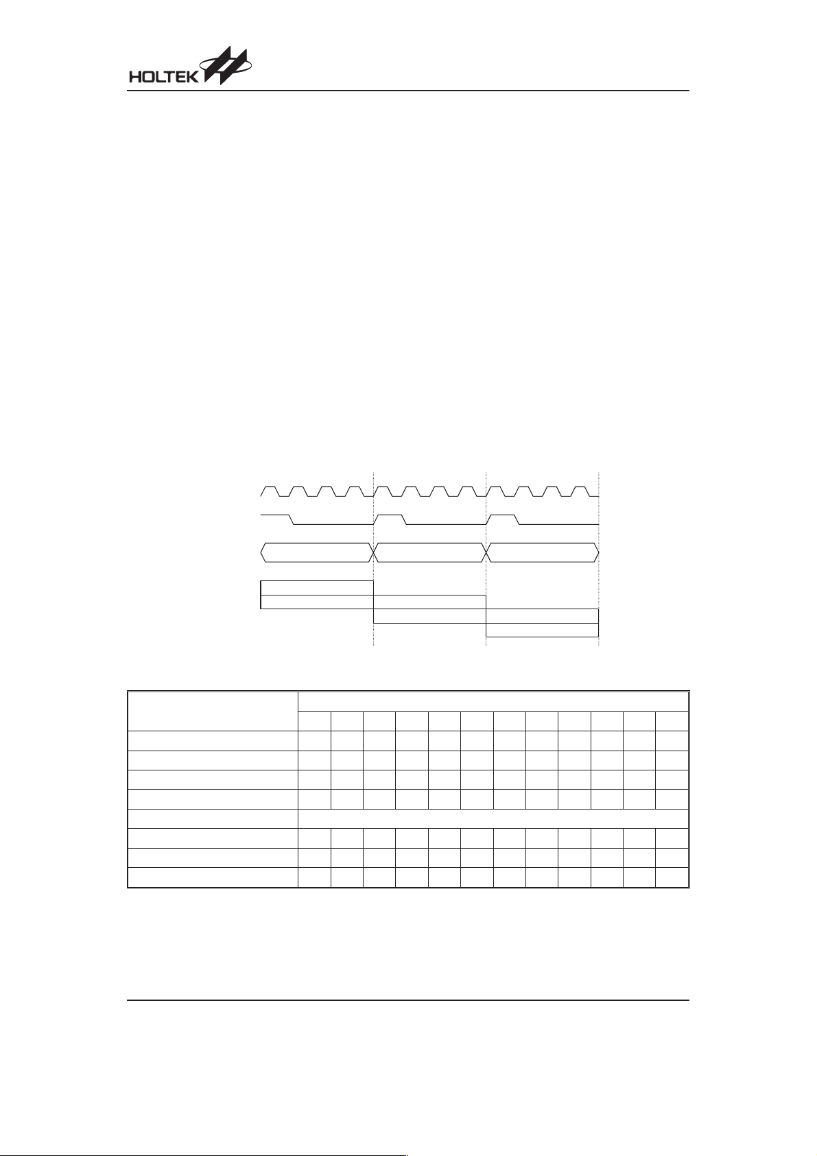
Execution Flow
The system clock for the microcontroller is derived from
either a crystal or an RC oscillator. The system clock is
internally divided into four non-overlapping clocks. One
instruction cycle consists of four system clock cycles.
Instruction fetching and execution are pipelined in such
a way that a fetch takes an instruction cycle while de
coding and execution takes the next instruction cycle.
However, the pipelining scheme causes each instruc
tion to effectively execute in a cycle. If an instruction
changes theprogram counter, two cycles are required to
complete the instruction.
Program Counter - PC
The programcounter controls the sequence in which the
instructions stored in program memory are executed
and whose contents specify full range of program mem
ory.
After accessing a program memory word to fetch an in
struction code, the contents of the program counter are
HT46R32/HT46R34
incremented byone. The program counter then points to
the memory word containing the next instruction code.
When executing a jump instruction, conditional skip ex
ecution, loading PCL register, subroutine call, initial re
set, internal interrupt, external interrupt or return from
subroutine, the PC manipulates the program transfer by
loading the address corresponding to each instruction.
The conditional skip is activated by instructions. Once
the condition is met, the next instruction, fetched during
the current instruction execution, is discarded and a
dummy cycle replaces it to get the proper instruction.
Otherwise proceed with the next instruction.
The lower byte of the program counter, PCL, is a read
able and writeable register. Moving data into the PCL
performs a short jump. The destination will be within 256
locations.
When a control transfer takes place, an additional
dummy cycle is required.
-
-
-
-
S y s t e m C l o c k
O S C 2 ( R C o n l y )
T 1 T 2 T 3 T 4 T 1 T 2 T 3 T 4 T 1 T 2 T 3 T 4
P C
P C P C + 1 P C + 2
F e t c h I N S T ( P C )
E x e c u t e I N S T ( P C - 1 )
F e t c h I N S T ( P C + 1 )
E x e c u t e I N S T ( P C )
F e t c h I N S T ( P C + 2 )
E x e c u t e I N S T ( P C + 1 )
Execution Flow
Mode
*11 *10 *9 *8 *7 *6 *5 *4 *3 *2 *1 *0
Program Counter
Initial Reset 000000000000
External Interrupt 000000000100
Timer/Event Counter Overflow 000000001000
A/D Converter Interrupt 000000001100
Skip Program Counter+2
Loading PCL *11 *10 *9 *8 @7 @6 @5 @4 @3 @2 @1 @0
Jump, Call Branch #11 #10 #9 #8 #7 #6 #5 #4 #3 #2 #1 #0
Return from Subroutine S11 S10 S9 S8 S7 S6 S5 S4 S3 S2 S1 S0
Program Counter
Note: PC11~PC8: Current Program Counter bits S11~S0: Stack register bits
#11~#0: Instruction Code bits @7~@0: PCL bits
For the HT46R32 device the Program Counter is 11 bits wide, i.e. from b10~b0, therefore the b11 column in
the table is not applicable.
Rev. 1.10 6 March 16, 2007

HT46R32/HT46R34
Program Memory - ROM
The program memory is used to store the program in
structions which are to be executed as well as table data
and interrupt entries. It is structured into 2K´14 bits for
the HT46R32 device and 4K x 15 bits for the HT46R34
device, which can be addressed by both the program
counter and table pointer.
Certain locations in the program memory are reserved
for use by the reset and by the interrupt vectors.
·
Location 000H
This vector is reserved for program initialisation. After
a device reset is initiated, the program will jump to this
location and begin execution.
·
Location 004H
This vector is used by the external interrupt INT
.Ifthe
external interrupt pin on the device receives a low go
ing edge,the program willjump to this location and be
gin execution if the external interrupt is enabled and
the stack is not full.
·
Location 008H
This vector is used by the Timer/Event Counter. If a
timer overflow occurs, the program will jump to this loca
tion and begin execution if the timer interrupt is enabled
and the stack is not full.
·
Location 00CH
This vector is used by the A/D converter. When an A/D
cycle conversion is complete, the program will jump to
this location and begin execution if the A/D interrupt is
enabled and the stack is not full.
·
Table location
Any location in the Program Memory space can be
used as a look-up table. The instructions ²TABRDC
[m]² (the current page, 1 page=256 words) and
²TABRDL [m]² (the last page) transfer the contents of
the lower-order byte to the specified data memory,
and the higher-order byte to TBLH. Only the destina
tion of the lower-order byte in the table is well-defined,
the other bits of the table word are transferred to the
lower portion of TBLH, and the remaining bits are read
as ²0². The Table Higher-order byte register (TBLH) is
read only. The table pointer (TBLP) is a read/write reg
ister, which indicates the table location. Before ac
cessing the table, the location must be placed in
TBLP. The TBLH register is read only and cannot be
0 0 0 H
-
0 0 4 H
0 0 8 H
0 0 C H
n 0 0 H
n F F H
7 0 0 H
7 F F H
-
-
D e v i c e I n i t i a l i z a t i o n P r o g r a m
E x t e r n a l I n t e r r u p t S u b r o u t i n e
T i m e r / E v e n t C o u n t e r I n t e r r u p t S u b r o u t i n e
A / D C o n v e r t e r I n t e r r u p t S u b r o u t i n e
L o o k - u p T a b l e ( 2 5 6 w o r d s )
L o o k - u p T a b l e ( 2 5 6 w o r d s )
1 4 b i t s
N o t e : n r a n g e s f r o m 0 t o 7
P r o g r a m
M e m o r y
Program Memory - HT46R32
0 0 0 H
0 0 4 H
-
0 0 8 H
0 0 C H
n 0 0 H
n F F H
F 0 0 H
F F F H
-
D e v i c e I n i t i a l i z a t i o n P r o g r a m
E x t e r n a l I n t e r r u p t S u b r o u t i n e
T i m e r / E v e n t C o u n t e r I n t e r r u p t S u b r o u t i n e
A / D C o n v e r t e r I n t e r r u p t S u b r o u t i n e
L o o k - u p T a b l e ( 2 5 6 w o r d s )
L o o k - u p T a b l e ( 2 5 6 w o r d s )
1 5 b i t s
N o t e : n r a n g e s f r o m 0 t o F
P r o g r a m
M e m o r y
Program Memory - HT46R34
-
-
restored. If the main routine and the ISR, Interrupt
Service Routine, both employ the table read instruc
tion, the contents of the TBLH in the main routine are
-
likely to be changed by the table read instruction used
Instruction
*11 *10 *9 *8 *7 *6 *5 *4 *3 *2 *1 *0
Table Location
TABRDC [m] P11 P10 P9 P8 @7 @6 @5 @4 @3 @2 @1 @0
TABRDL [m] 1111@7@6@5@4@3@2@1@0
Table Location
Note: *11~*0: Table location bits P11~P8: Current program counter bits
@7~@0: Table pointer bits
For the HT46R32 device the Table address is 11 bits wide, i.e. from b10~b0, therefore the b11 column in the
table is not applicable.
Rev. 1.10 7 March 16, 2007

HT46R32/HT46R34
in the ISR. In such a case errors can occur. Therefore,
using the table read instruction in the main routine and
the ISR simultaneously should be avoided. However,
if the table read instruction has to be used in both the
main routine and the ISR, the interrupt is should be
disabled prior to the table read instruction. It should
not be re-enabled until the TBLH has been backed up.
All table related instructions require two cycles to
complete their operation. These areas may function
as normal program memory depending upon require
ments.
Stack Register - STACK
This is a special part of the memory which is used to
save the contents of the program counter only. The
stack is organized into 6 levels and is neither part of the
data nor part of the program space, and is neither read
able nor writeable. The activated level is indexed by the
stack pointer, known as stack pointer, and is also neither
readable nor writeable. At a subroutine call or interrupt
acknowledgment, the contents of the program counter
are pushed onto the stack. At the end of a subroutine or
an interrupt routine, signaled by a return instruction,
RET or RETI, the program counter is restored to its pre
vious value from the stack. After a device reset, the
stack pointer will point to the top of the stack.
If the stack is full and a non-masked interrupt takes
place, the interrupt request flag will be recorded but the
acknowledgment will be inhibited. When the stack
pointer is decremented, using a RET or RETI instruction, the interrupt will be serviced. This feature prevents
a stack overflow allowing the programmer to use the
structure more easily. In a similar case, if the stack is full
and a ²CALL² is subsequently executed, stack overflow
occurs and the first entry will be lost. Only the most recent 6 return addresses are stored.
Data Memory - RAM
The data memory has a structure of 110´8 bits for the
HT46R32 device and 215 x 8 bits for the HT46R34 de
vice. The data memory is divided into two functional
groups: special function registers and general purpose
data memory. The general purpose memory has a
structure of 88 x 8 bits for the HT46R32 device and
192bits x 8 bits for the HT46R34 device. Most locations
are read/write, but some are read only.
The remaining space between the end of the Special
Purpose Data Memory and the beginning of the General
Purpose Data Memory is reserved for future expanded
usage, reading these locations will obtain a result of
²00H². The general purpose data memory, addressed
from 28H to 7FH in the HT46R32, and from 40H to FFH
in the HT46R34, is used for user data and control infor
mation under instruction commands. All of the data
memory areas can handle arithmetic, logic, increment,
decrement and rotate operations directly. Except for
some dedicated bits, each bit in the data memory can
be set and reset by the ²SET [m].i² and ²CLR [m].i² in
structions. They are also indirectly accessible through
memory pointer register, MP.
I n d i r e c t A d d r e s s i n g R e g i s t e r
0 0 H
0 1 H
0 2 H
0 3 H
0 4 H
0 5 H
0 6 H
-
0 7 H
0 8 H
0 9 H
0 A H
0 B H
0 C H
0 D H
0 E H
0 F H
1 0 H
-
1 1 H
1 2 H
1 3 H
1 4 H
1 5 H
1 6 H
1 7 H
1 8 H
1 9 H
1 A H
-
1 B H
1 C H
1 D H
1 E H
1 F H
2 0 H
2 1 H
2 2 H
2 3 H
2 4 H
2 7 H
2 8 H
7 F H
M P
A C C
P C L
T B L P
T B L H
S T A T U S
I N T C
T M R
T M R C
S p e c i a l P u r p o s e
P A
P A C
P B
P B C
P D
P D C
P W M 0
P W M 1
O P A C
A D R L
A D R H
A D C R
A C S R
H T 4 6 R 3 2 / H T 4 6 R 3 4
G e n e r a l P u r p o s e
D a t a M e m o r y
( 8 8 B y t e s )
H T 4 6 R 3 2 H T 4 6 R 3 4
D a t a M e m o r y
: U n u s e d
R e a d a s " 0 0 "
2 4 H
3 9 H
4 0 H
F F H
G e n e r a l P u r p o s e
D a t a M e m o r y
RAM Mapping
Indirect Addressing Register
Location 00H is an indirect addressing register that is
not physicallyimplemented. Any read/write operation on
[00H] accesses data memory pointed to by the MP
register. Reading location 00H itself indirectly will return
the result00H. Writing indirectly results in no operation.
For the HT46R32 device the memory pointer register, MP,
is a 7-bit register, while for the HT46R34 device it is an
8-bit register. For the HT46R32 device, bit 7 of MP is un
defined and if read will return the result ²1², any write op
eration will only transfer the lower 7-bits of data to MP.
Accumulator
The accumulator is closely related to ALU operations
and can carry out immediate data operations. Any data
movement between two data memory locations must
pass through the accumulator.
-
( 1 9 2 B y t e s )
-
-
Rev. 1.10 8 March 16, 2007

HT46R32/HT46R34
Arithmetic and Logic Unit - ALU
This circuit performs 8-bit arithmetic and logic opera
tions. The ALU provides the following functions:
·
Arithmetic operations - ADD, ADC, SUB, SBC, DAA
·
Logic operations - AND, OR, XOR, CPL
·
Rotation - RL, RR, RLC, RRC
·
Increment and Decrement - INC, DEC
·
Branch decision - SZ, SNZ, SIZ, SDZ ....
The ALU not only saves the results of a data operation but
also changes the status register.
Status Register - STATUS
This 8-bit register contains the zero flag (Z), carry flag
(C), auxiliary carry flag (AC), overflow flag (OV), power
tion operations related to the status register may give
different results from those intended. The TO flag
-
can be affected only by system power-up, a WDT
time-out or executing the ²CLR WDT² or ²HALT² in
struction. The PDF flag can be affected only by exe
cuting the ²HALT² or ²CLR WDT² instruction or a
system power-up.
The Z, OV, AC and C flags generally reflect the status of
the latest operations.
In addition, on entering the interrupt sequence or exe
cuting the subroutine call, the status register will not be
pushed onto the stack automatically. If the contents of
the status are important and if the subroutine can cor
rupt the status register, precautions must be taken to
save it properly.
down flag (PDF), and watchdog time-out flag (TO). It
also records the status information and controls the op
eration sequence.
With the exception of the TO and PDF flags, bits in
the status register can be altered by instructions like
most other registers. Any data written into the status
register will not change the TO or PDF flag. In addi
Interrupt
-
The devices provide an external interrupt, an internal
timer/event counter interrupt and an A/D converter inter
rupt. The Interrupt Control Register, INTC, contains the
interrupt control bits to set the enable or disable and the
interrupt request flags.
-
Bit No. Label Function
C is set if an operation results in a carry during an addition operation or if a borrow does not
0C
take place during a subtraction operation, otherwise C is cleared. C is also affected by a rotate through carry instruction.
1AC
AC is set if an operation results in a carry out of the low nibbles in addition or no borrow from
the high nibble into the low nibble in subtraction, otherwise AC is cleared.
2 Z Z is set if the result of an arithmetic or logic operation is zero, otherwise Z is cleared.
3OV
4 PDF
5TO
6, 7
OV is set if an operation results in a carry into the highest-order bit but not a carry out of the
highest-order bit, or vice versa, otherwise OV is cleared.
PDF iscleared by a system power-up or executing the ²CLR WDT² instruction. PDF is set by
executing the ²HALT² instruction.
TO is cleared by a system power-up or executing the ²CLR WDT²or ²HALT²instruction. TO
is set by a WDT time-out.
¾ Unused bit, read as ²0²
-
-
-
-
-
Status (0AH) Register
Bit No. Label Function
0 EMI Controls the master (global) interrupt (1=enabled; 0=disabled)
1 EEI Controls the external interrupt (1=enabled; 0=disabled)
2 ETI Controls the Timer/Event Counter interrupt (1=enabled; 0=disabled)
3 EADI Controls the A/D converter interrupt (1=enabled; 0=disabled)
4 EIF External interrupt request flag (1=active; 0=inactive)
5 TF Internal Timer/Event Counter request flag (1=active; 0=inactive)
6 ADF A/D converter request flag (1=active; 0=inactive)
7
¾ Unused bit, read as ²0²
INTC (0BH) Register
Rev. 1.10 9 March 16, 2007

HT46R32/HT46R34
Once an interrupt subroutine is serviced, all the other in
terrupts will be blocked by clearing the EMI bit. This
scheme may prevent any further interrupt nesting. Other
interrupt requests may happen during this interval but
only the interrupt request flag is recorded. If a certain in
terrupt requires servicing within the service routine, the
EMI bit and the corresponding bit in INTC may be set to
allow interrupt nesting. If the stack is full, the interrupt re
quest will not be acknowledged, even if the related inter
rupt is enabled, until the stack pointer is decremented. If
immediate service is desired, the stack must be pre
vented from becoming full.
All interrupts have a wake-up capability. As an interrupt
is serviced, a control transfer occurs by pushing the pro
gram counter onto the stack, followed by a branch to a
subroutine at a specified location in the program mem
ory. Only the program counter is pushed onto the stack.
If the contents of the register or status register are al
tered by the interrupt service program which corrupts
the desired control sequence, the contents should be
saved in advance.
External interrupts are triggered by a high to low transi
tion on the INT
pin, which will set the related interrupt re
quest flag, EIF, which is bit 4 of INTC. When the interrupt
is enabled, the stack is not full and the external interrupt
is active, a subroutine call to location 04H will occur. The
interrupt request flag, EIF, and EMI bits will be cleared to
disable other interrupts.
The internal timer/event counter interrupt is initialised by
setting the timer/event counter interrupt request flag, TF,
which is bit 5 of INTC, caused by a timer overflow. When
the interrupt is enabled, the stack is not full and the TF
bit is set, a subroutine call to location 08H will occur. The
related interrupt request flag, TF, will be reset and the
EMI bit cleared to disable further interrupts.
The A/D converter interrupt is initialised by setting the
A/D converter request flag, ADF, which is bit 6 of INTC,
caused by an end of A/D conversion. When the interrupt
is enabled, the stack is not full and the ADF bit is set, a
subroutine call to location 0CH will occur. The related in
terrupt request flag, ADF, will be reset and the EMI bit
cleared to disable further interrupts.
During the execution of an interrupt subroutine, other in
terrupt acknowledgments are held until the RETI in
struction is executed or the EMI bit and the related
interrupt control bit are set to 1. Of course, the stack
must not be full. To return from the interrupt subroutine,
a RET or RETI instruction may be executed. A RETI in
struction will set the EMI bit to enable an interrupt ser
vice, but a RET instruction will not.
Interrupts, occurring in the interval between the rising
edges of two consecutive T2 pulses, will be serviced on
the latter of the two T2 pulses, if the corresponding inter
rupts are enabled. In the case of simultaneous requests
the following table shows the priority that is applied.
These can be masked by resetting the EMI bit.
-
Interrupt Source Priority Vector
External Interrupt 1 004H
Timer/Event Counter Overflow 2 008H
A/D Converter Interrupt 3 00CH
-
Once the interrupt request flags, TF, EIF, ADF, are set,
-
they will remain in the INTC register until the interrupts
are serviced or cleared by a software instruction.
-
It is recommended that a program does not use the CALL
subroutine within the interrupt subroutine. Interrupts of
ten occur in an unpredictable manner or need to be ser
-
viced immediately in some applications. If only one stack
is left and enabling the interrupt is not well controlled, the
-
original control sequence will be damaged once the
²CALL² operates in the interrupt subroutine.
-
Oscillator Configuration
There are two oscillator circuits in the microcontroller,
namely an RC oscillator and a crystal oscillator, the
-
choice of which is determined by a configuration option.
-
When the system enters the Power-down mode the sys
tem oscillator stops and ignores external signals to con
serve power.
If an RC oscillator is used, an external resistor between
OSC1 and VSS is required whose resistance value
must range from 24kW to 1MW. The system clock, divided by 4, can be monitored on pin OSC2 if a pull-high
resistor is connected. This signal can be used to synchronise external logic. The RC oscillator provides the
most cost effective solution, however the frequency of
oscillation may vary with VDD, temperature and the
process variations. It is, therefore, not suitable for tim
ing sensitive operations where an accurate oscillator
frequency is desired.
If the Crystal oscillator is used, a crystal across OSC1
and OSC2 is needed to provide the feedback and phase
shift required for the oscillator; no other external compo
-
nents are required. Instead of a crystal, a resonator can
also be connected between OSC1 and OSC2 to get a
frequency reference, but two external capacitors in
-
OSC1 and OSC2 are required, If the oscillating fre
-
quency is less than 1MHz.
The WDT oscillator is a free running on-chip RC oscilla
tor, and requires no external components. Even if the
system enters the power down mode, the system clock
-
-
O S C 1
-
O S C 2
C r y s t a l O s c i l l a t o r R C O s c i l l a t o r
V
D D
4 7 0 p F
f
/ 4
S Y S
System Oscillator
-
-
-
-
-
-
-
-
O S C 1
O S C 2
Rev. 1.10 10 March 16, 2007

HT46R32/HT46R34
is stopped, but the WDT oscillator keeps running with a
period of approximately 65ms at 5V. The WDT oscillator
can be disabled by a configuration option to conserve
power.
Watchdog Timer - WDT
The WDT clock source comes from either its own inte
grated RC oscillator,known as the WDT oscillator, or the
instruction clock, which is the system clock divided by 4.
The choice of which one is used is decided by a
configuration option. This timer is designed to prevent a
software malfunction or sequence from jumping to an
unknown location with unpredictable results. The
Watchdog Timer can be disabled by a configuration op
tion. If the Watchdog Timer is disabled, all the execu
tions related to the WDT result in no operation.
Once the internal WDT oscillator (RC oscillator with a
period of 65ms at 5V nominal) is selected, it is divided by
32768~65536 to get a time-out period of approximately
2.1s~4.3s. This time-out period may vary with tempera
tures, VDD and process variations. If the WDT oscillator
is disabled, the WDT clock may still come from the in
struction clock and operate in the same manner except
that in the Power-down state the WDT may stop count
ing and lose its protecting purpose. In this situation the
logic can only be restarted by external logic.
If the device operates in a noisy environment, using the
on-chip RC oscillator (WDT OSC) is strongly recommended, since the HALT instruction will stop the system
clock.
The WDT overflow under normal operation will initialise
a ²chip reset² and set the status bit ²TO². But in the
Power-down mode, the overflow will initialisze a ²warm
reset², andonly the programcounter and SPare reset to
zero. To clear the contents of the WDT, three methods
are adopted; external reset (a low level on the RES
pin),
a software instruction and a HALT instruction. The soft
ware instruction include ²CLR WDT² and the other set ²CLR WDT1² and ²CLR WDT2². Of these two types of
instruction, only one can be active depending on the
configuration option -²CLR WDT times selection op
tion².Ifthe²CLR WDT² is selected (i.e. CLR WDT times
equal one), any execution of the ²CLR WDT² instruction
will clear the WDT. In the case that ²CLR WDT1² and
²CLR WDT2² are chosen (i.e. CLR WDT times equal
two), these two instructions must be executed to clear
-
the WDT; otherwise, the WDT may reset the chip as a
result of time-out.
Power Down Operation - HALT
The HALT mode is initialised by the ²HALT² instruction
and results in the following...
·
-
-
The system oscillator will be turned off but the WDT
oscillator keeps running (if the WDT oscillator is se
lected).
·
The contents of the on chip Data Memory and regis
ters remain unchanged.
·
WDT will be cleared and start counting again (if the
WDT clock is from the WDT oscillator).
-
·
All of the I/O ports maintain their original status.
·
-
The PDF flag is set and the TO flag is cleared.
The system can leave the HALT mode by means of an
external reset, an interrupt, an external falling edge sig
-
nal on port A or a WDT overflow. An external reset
causes a device initialisation and the WDT overflow performs a ²warm reset². After the TO and PDF flags are
examined, the reason for the chip reset can be determined. The PDF flag is cleared by a system power-up or
executing the ²CLR WDT² instruction and is set when
executing the ²HALT² instruction. The TO flag is set if
the WDT time-out occurs, and causes a wake-up that
only resets the program counter and Stack Pointer; the
others keep their original status.
The port A wake-up and interrupt methods can be con
sidered as a continuation of normal execution. Each bit
in port A can be independently selected to wake up the
-
device by the options. Awakening from an I/O port stim
ulus, the program will resume execution of the next in
struction. If it is awakening from an interrupt, two
sequences may happen. If the related interrupt is dis
-
-
-
-
-
-
-
-
S y s t e m C l o c k / 4
f
W D T
O S C
O p t i o n
S e l e c t
S
8 - b i t C o u n t e r
7 - b i t C o u n t e r
T
T
W D T T i m e - o u t
1 5 1 6
f
/ 2 ~ fS/ 2
S
C L R W D T
Watchdog Timer
Rev. 1.10 11 March 16, 2007
HT46R32/HT46R34
abled or the interrupt is enabled but the stack is full, the
program will resume execution at the next instruction. If
the interrupt is enabled and the stack is not full, the regu
lar interrupt response takes place. If an interrupt request
flag is set to ²1² before entering the HALT mode, the
wake-up functionof the related interrupt will be disabled.
Once a wake-up event occurs, it takes 1024 t
SYS
(sys
tem clock period) to resume normal operation. In other
words, a dummy period will be inserted after wake-up. If
the wake-up results from an interrupt acknowledgment,
the actual interrupt subroutine execution will be delayed
by one or more cycles. If the wake-up results in the next
instruction execution, this will be executed immediately
after the dummy period is finished.
To minimise power consumption, all the I/O pins should
be carefully managed before entering the status.
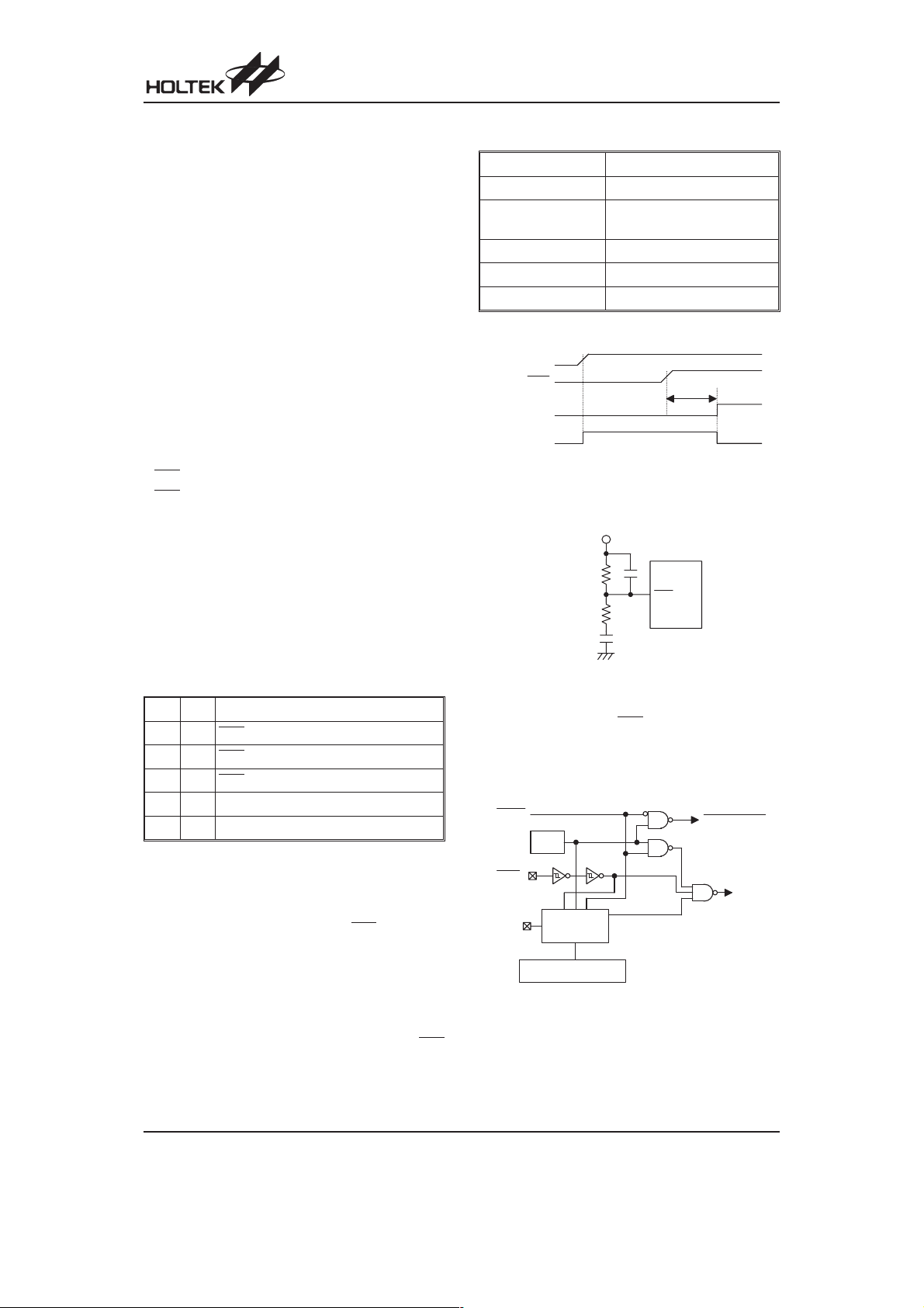
Reset
There are three ways in which a reset can occur:
·
RES reset during normal operation
·
RES reset during HALT
·
WDT time-out reset during normal operation
The WDT time-out during HALT is different from other
chip reset conditions, since it can perform a ²warm re
set² that resets only the program counter and stack
pointer, leaving the other circuits in their original state.
Some registers remain unchanged during other reset
conditions. Most registers are reset to the ²initial condition² when the reset conditions are met. By examining
the PDF and TO flags, the program can distinguish between different ²chip resets².
TO PDF RESET Conditions
0 0 RES
u u RES
0 1 RES
reset during power-up
reset during normal operation
wake-up HALT
1 u WDT time-out during normal operation
1 1 WDT wake-up HALT
Note: ²u² means ²unchanged²
To guarantee that the system oscillator is started and
stabilized, the SST (System Start-up Timer) provides an
extra-delay of 1024 system clock pulses when the sys
tem reset (power-up, WDT time-out or RES reset) or the
system awakes from the HALT state.
When a system reset occurs, the SST delay is added
during the reset period. Any wake-up from HALT will en
able the SST delay.
An extra option load time delay is added during system
reset (power-up, WDT time-out at normal mode or RES
reset).
The functional unit chip reset status are shown below.
Program Counter 000H
Interrupt Disable
WDT
Timer/Event Counter Off
Clear. After master reset,
WDT begins counting
Input/Output Ports Input mode
Stack Pointer Points to the top of the stack
V D D
R E S
S S T T i m e - o u t
C h i p R e s e t
t
S S T
Reset Timing Chart
V
D D
0 . 0 1mF *
-
1 0 0 k
W
R E S
1 0 k
W
0 . 1mF *
Reset Circuit
Note:
²*² Ensure that the length of the wiring, which is
connected to the RES
pin is as short as possi-
ble, to avoid noise interference.
H A L T
W D T
R E S
-
O S C 1
S S T
1 0 - b i t R i p p l e
C o u n t e r
S y s t e m R e s e t
-
Reset Configuration
W a r m R e s e t
C o l d
R e s e t
Rev. 1.10 12 March 16, 2007

The registers¢ states are summarised in the following table.
HT46R32/HT46R34
Register
MP - HT46R32 1xxx xxxx 1uuu uuuu 1uuu uuuu 1uuu uuuu 1uuu uuuu
MP - HT46R34 xxxx xxxx uuuu uuuu uuuu uuuu uuuu uuuu uuuu uuuu
ACC xxxx xxxx uuuu uuuu uuuu uuuu uuuu uuuu uuuu uuuu
PCL 0000 0000 0000 0000 0000 0000 0000 0000 0000 0000
TBLP xxxx xxxx uuuu uuuu uuuu uuuu uuuu uuuu uuuu uuuu
TBLH - HT46R32 --xx xxxx --uu uuuu --uu uuuu --uu uuuu --uu uuuu
TBLH - HT46R34 -xxx xxxx -uuu uuuu -uuu uuuu -uuu uuuu -uuu uuuu
STATUS --00 xxxx --1u uuuu --uu uuuu --01 uuuu --11 uuuu
INTC -000 0000 -000 0000 -000 0000 -000 0000 -uuu uuuu
TMR xxxx xxxx xxxx xxxx xxxx xxxx xxxx xxxx uuuu uuuu
TMRC 00-0 1000 00-0 1000 00-0 1000 00-0 1000 uu-u uuuu
PA 1111 1111 1111 1111 1111 1111 1111 1111 uuuu uuuu
PAC 1111 1111 1111 1111 1111 1111 1111 1111 uuuu uuuu
PB 1111 1111 1111 1111 1111 1111 1111 1111 uuuu uuuu
PBC 1111 1111 1111 1111 1111 1111 1111 1111 uuuu uuuu
PD ---- 1111 ---- 1111 ---- 1111 ---- 1111 ---- uuuu
PDC ---- 1111 ---- 1111 ---- 1111 ---- 1111 ---- uuuu
PWM0 xxxx xxxx xxxx xxxx xxxx xxxx xxxx xxxx uuuu uuuu
PWM1 xxxx xxxx xxxx xxxx xxxx xxxx xxxx xxxx uuuu uuuu
OPAC 0000 1000 0000 1000 0000 1000 0000 1000 uuuu uuuu
ADRL xxxx ---- xxxx ---- xxxx ---- xxxx ---- uuuu ----
ADRH xxxx xxxx xxxx xxxx xxxx xxxx xxxx xxxx uuuu uuuu
ADCR 0100 0000 0100 0000 0100 0000 0100 0000 uuuu uuuu
ACSR 1--- --00 1--- --00 1--- --00 1--- --00 u--- --uu
Reset
(Power On)
WDT Time-out
(Normal Operation)
RES
(Normal Operation)
Reset
RES Reset
(HALT)
WDT Times-out
(HALT)*
Note:
²*² stands for warm reset
²u² stands for unchanged
²x² stands for unknown
Rev. 1.10 13 March 16, 2007

HT46R32/HT46R34
Timer/Event Counter
A timer/event counter is implemented in the
microcontroller. The timer/event counter contains an
8-bit programmable count-up counter whose clock
source may come from an external source or from the
system clock.
Using an external clock input allows the user to count
external events, measure time internals or pulse widths,
or generate an accurate time base. While using the in
ternal clock allows the user to generate an accurate time
base.
The timer/event counter can generate a PFD signal by
using the external or internal clock. The PFD frequency
is determined by the equation f
/[2´(256-N)].
INT
There are 2 registers related to the timer/event counter;
TMR and TMRC. Two physical registers are mapped to
the TMR location. Writing to TMR places the start value
in the timer/event counter preload register, while read
ing TMR retrieves the contents of the timer/event coun
ter. The TMRC register is a timer/event counter control
register, which defines some options.
The TM0 and TM1 bits define the operating mode. The
event count mode is used to count external events,
which means the clock source emanates from the exter
nal TMR pin. The timer mode functions as a normal
timer with the clock source coming from the f
INT
clock.
The pulse width measurement mode can be used to count
the high or low level duration of the external signal on TMR.
The counting is based on f
INT
.
In the event count or timer mode, once the timer/event
counter starts counting, it will count from the current
contents in the timer/event counter to FFH. Once an
overflow occurs, the counter is reloaded from the
timer/event counter preload register and generates an
interrupt request flag, TF, which is bit 5 of INTC, at the
same time.
In the pulse width measurement mode with the TON and
TE bits equal to one, once TMR has received a transient
-
from low to high (or high to low if the TE bits is ²0²) it will
start counting until TMR returns to the original level and
resets the TON bit. The measured result will remain in the
timer/event counter even if the activated transient occurs
again. Therefore only a one cycle measurement is made.
Not until the TON bit is once again set, will the cycle mea
surement function again if further transient pulses are re
ceived. Note that, in this operating mode, the timer/event
counter starts counting not according to the logic level but
according to the transient edges. In the case of counter
overflows, the counter is reloaded from the timer/event
counter preload register and issues the interrupt request
just like the other two modes. To enable the counting op
eration, the timer ON bit,TON, which is bit 4 of TMRC,
should be set to 1. In the pulse width measurement
mode, the TON bit will be cleared automatically after the
measurement cycle is completed. But in the other two
modes the TON bit can only be reset by instructions. The
overflow of the timer/event counter is one of the wake-up
sources. No matter what the operation mode is, writing a
0 to ETI can disable the interrupt service.
Bit No. Label Function
Defines the prescaler stages, PSC2, PSC1, PSC0=
000: f
INT=fSYS
0
1
2
PSC0
PSC1
PSC2
010: f
011: f
100: f
101: f
110: f
111: f
001: f
INT=fSYS
INT=fSYS
INT=fSYS
INT=fSYS
INT=fSYS
INT=fSYS
INT=fSYS
/2
/4
/8
/16
/32
/64
/128
Defines the TMR active edge of the timer/event counter:
In Event Counter Mode (TM1,TM0)=(0,1):
1:count on falling edge;
3TE
0:count on rising edge
In Pulse Width measurement mode (TM1,TM0)=(1,1):
1: start counting on the rising edge, stop on the falling edge;
0: start counting on the falling edge, stop on the rising edge
4 TON
5
¾ Unused bits, read as ²0²
Enable or disable the timer counting
(0=disable; 1=enable)
Defines the operating mode (TM1, TM0)=
6
7
TM0
TM1
01=Event count mode (external clock)
10=Timer mode (internal clock)
11=Pulse width measurement mode
00=Unused
TMRC (0EH) Register
-
-
-
Rev. 1.10 14 March 16, 2007

HT46R32/HT46R34
P W M
( 6 + 2 ) C o m p a r e
f
S Y S
8 - s t a g e P r e s c a l e r
8 - 1 M U X
P S C 2 ~ P S C 0
T M R
T o P D 0 C i r c u i t
f
I N T
T E
T M 1
T M 0
8 - B i t T i m e r / E v e n t
C o u n t e r P r e l o a d
R e g i s t e r
D a t a B u s
R e l o a d
P u l s e W i d t h
T M 1
M e a s u r e m e n t
T M 0
M o d e C o n t r o l
T O N
Timer/Event Counter
In the case of a timer/event counter OFF condition, writ
ing data to the timer/event counter preload register will
also reloadthat data tothe timer/event counter. But if the
timer/event counter is turned on, data written to it will
only be kept in the timer/event counter preload register.
The timer/event counter will still operate until an over
flow occurs. When the timer/event counter is read, the
clock will be blocked to avoid errors. As clock blocking
may results in a counting error, this must be taken into
consideration by the programmer.
Bit0~bit2 of the TMRC register can be used to define the
pre-scaling stages of the internal clock sources of the
timer/event counter. The definitions are as shown. The
overflow signal of timer/event counter can be used to
generate the PFD signal.
Input/Output Ports
There are 19 bidirectional input/output lines in the
microcontroller, labeled as PA, PB, PC and PD, which
are mapped to the data memory of [12H], [14H], [16H]
P F D
P A 3
C o n t r o l B i t
D
C K
Q
S
D a t a B i t
D
C K
Q
S
Q
Q
M
U
X
D a t a B u s
W r i t e C o n t r o l R e g i s t e r
C h i p R e s e t
R e a d C o n t r o l R e g i s t e r
W r i t e D a t a R e g i s t e r
( P D 0 o r P W M )
R e a d D a t a R e g i s t e r
S y s t e m W a k e - u p
( P A o n l y )
I N T f o r P A 5 O n l y
T M R f o r P A 4 O n l y
Input/Output Ports
8 - B i t T i m e r / E v e n t
C o u n t e r
and [18H] respectively. All of these I/O ports can be
-
O v e r f l o w
t o I n t e r r u p t
1 / 2
P F D
used for input and output operations. For input opera
tion, these ports are non-latching, that is, the inputs
must be ready at the T2 rising edge of instruction ²MOV
A,[m]² (m=12H, 14H, 16H or 18H). For output operation,
-
all the data is latched and remains unchanged until the
output latch is rewritten.
Each I/O line has its own control register (PAC, PBC,
PCC, PDC) to control the input/output configuration.
With this control register, CMOS output or Schmitt trig
ger input with or without pull-high resistor structures can
be reconfigured dynamically (i.e. on-the-fly) under software control. To function as an input, the corresponding
latch of the control register must write ²1². The input
source also depends on the control register. If the control register bit is ²1², the input will read the pad state. If
the control register bit is ²0², the contents of the latches
will move to the internal bus. The latter is possible in the
²read-modify-write² instruction.
V
P u l l - H i g h
O p t i o n
W a k e - u p o p t i o n
M
U
X
P F D E N
( P A 3 )
D D
P A 0 ~ P A 2
P A 3 / P F D
P A 4 / T M R
P A 5 / I N T
P A 6 , P A 7
P B 0 / A N 0 ~ P B 3 / A N 3
P B 4 ~ P B 7
P D 0 / P W M 0
P D 1 / P W M 1
P D 2
P D 3
-
-
Rev. 1.10 15 March 16, 2007

HT46R32/HT46R34
After a device reset, the input/output lines will default to
inputs and remain at a high level or floating state, de
pendent upon the pull-high configuration options. Each
bit of these input/output latches can be set or cleared by
the ²SET [m].i² and ²CLR [m].i² (m=12H, 14H, 16H or
18H) instructions.
Some instructions first input data and then follow the
output operations. For example, ²SET [m].i², ²CLR
[m].i², ²CPL [m]², ²CPLA [m]² read the entire port states
into the CPU, execute the defined operations
(bit-operation), and then write the results back to the
latches or the accumulator.
Each line of port A has the capability of waking-up the
device.
Each I/O line has a pull-high option. Once the pull-high
configuration option is selected, the I/O line has a
pull-high resistor, otherwise, there¢s none. Take note
that a non-pull-high I/O line operating in input mode will
cause a floating state.
Pin PA3 is pin-shared with the PFD signal. If the PFD
configuration option is selected, the output signal in the
output modefor PA3 will be the PFD signal generated by
the timer/event counter overflow signal. The input mode
always retains its original functions. Once the PFD op
tion is selected, the PFD output signal is controlled by
the PA3 data register only. Writing a ²1² to the PA3 data
register will enable the PFD output function and writing
²0² will force the PA3 to remain at ²0². The I/O functions
for PA3 are shown below.
I/O
Mode
PA3
I/P
(Normal)
Logical
Input
O/P
(Normal)
Logical
Output
I/P
(PFD)
Logical
Input
O/P
(PFD)
PFD
(Timer on)
Note: The PFD frequency is the timer/event counter
overflowfrequencydivided by2.
Pins PA5 and PA4 are pin-shared with INT
and TMR
pins respectively.
The PB can also be used as A/D converter inputs. The
A/D function will be described later. There are two PWM
functions shared with pins PD0 and PD1. If the PWM
functions are enabled, the PWM signals will appear on
PD0 and PD1, the pins are setup as outputs. Writing a
²1² to the PD0 or PD1 data register will enable the PWM
outputs to function while writing a ²0² will force the PD0
and PD1 outputs to remain at ²0². The I/O functions of
PD0 and PD1 are as shown.
I/O
Mode
PD0
PD1
I/P
(Normal)
Logical
Input
O/P
(Normal)
Logical
Output
I/P
(PWM)
Logical
Input
O/P
(PWM)
PWM0
PWM1
It is recommended that unused I/O lines should be setup
as output pins by software instructions to avoid consum
ing power under input floating states.
PWM
The microcontroller provides a 2 channel (6+2) bits
PWM0/PWM1 output shared with PD0/PD1. The PWM
channel has its data register denoted as PWM0 and
PWM1. The frequency source of the PWM counter co
mes from f
. The PWM register is an eight bit register.
SYS
Once PD0/PD1 are selected as PWM outputs and the
output function of PD0/PD1 is enabled (PDC.0=²0² or
PDC.1=²0²), writing a 1 to the PD0/PD1 data register
will enable the PWM output function while writing a ²0²
will force the PD0/PD1 outputs to stay at ²0².
A PWM cycle is divided into four modulation cycles
(modulation cycle 0~modulation cycle 3). Each modula
tion cycle has 64 PWM input clock period. In a (6+2) bit
PWM function, the contents of the PWM register is di
vided into two groups. Group 1 of the PWM register is
denoted by DC which is the value of PWM.7~PWM.2.
Group 2 is denoted by AC which is the value of
PWM.1~PWM.0.
In a PWM cycle, the duty cycle of each modulation cycle
is shown in the table.
Parameter AC (0~3) Duty Cycle
Modulation cycle i
i<AC
(i=0~3)
i³AC
The modulation frequency, cycle frequency and cycle
duty of the PWM output signal are summarized in the
following table.
PWM
Modulation
Frequency
f
/64 f
SYS
PWM Cycle
Frequency
/256 [PWM]/256
SYS
-
-
-
-
DC+1
64
DC
64
PWM Cycle
Duty
Rev. 1.10 16 March 16, 2007

f
/ 2
S Y S
[ P W M ] = 1 0 0
P W M
[ P W M ] = 1 0 1
P W M
[ P W M ] = 1 0 2
P W M
[ P W M ] = 1 0 3
P W M
2 5 / 6 4
2 6 / 6 4
2 6 / 6 4
2 6 / 6 4
P W M m o d u l a t i o n p e r i o d : 6 4 / f
M o d u l a t i o n c y c l e 0
HT46R32/HT46R34
2 5 / 6 4 2 5 / 6 4 2 5 / 6 4
2 5 / 6 4
2 6 / 6 4
2 6 / 6 4
S Y S
M o d u l a t i o n c y c l e 1 M o d u l a t i o n c y c l e 2 M o d u l a t i o n c y c l e 3 M o d u l a t i o n c y c l e 0
P W M c y c l e : 2 5 6 / f
2 5 / 6 4
2 5 / 6 4
2 6 / 6 4 2 5 / 6 4
S Y S
2 5 / 6 4
2 5 / 6 4
PWM
2 5 / 6 4
2 6 / 6 4
2 6 / 6 4
2 6 / 6 4
A/D Converter
A 4 channel 12-bit resolution A/D converter is imple
mented in the microcontrollers. The reference voltage
for the A/D is VDD. The A/D converter contains 4 special
registers, which are; ADRL, ADRH, ADCR and ACSR.
The ADRH and ADRL registers are the A/D conversion
result register higher-order byte and lower-order byte
and are read-only. After the A/D conversion has completed, the ADRL and ADRH registers should be read to
get the conversion result data. The ADCR register is an
A/D converter control register, which defines the A/D
channel number, analog channel select, start A/D conversion control bit and the end of A/D conversion flag. It
is used to start an A/D conversion, define the PB configuration, select the converted analog channel, and give
the START bit a raising edge and a falling edge
(0®1®0). At the end of an A/D conversion, the EOCB
bit is cleared and an A/D converter interrupt occurs, if
the A/D converter interrupt is enabled. The ACSR
register is an A/D clock setting register, which is used to
select the A/D clock source.
The A/D converter control register is used to control the
A/D converter. Bit2~bit0 of the ADCR regsiter are used
to select an analog input channel. There are a total of
four channels to select. Bit5~bit3 of the ADCR register
are used to set the PB configurations. PB can be config
ured as an analog input or as a digital I/O line decided by
these 3 bits. Once a PB line is selected as an analog in
put, the I/O functions and pull-high resistor of this I/O
line are disabled, and the A/D converter circuit is
powered on. The EOCB bit, bit6 of ADCR, is the end of
A/D conversion flag. This bit is monitored to check when
the A/D conversion has completed. The START bit of
the ADCR register is used to initiate the A/D conversion
process. When the START bit is provided with a raising
edge and then a falling edge, the A/D conversion pro
cess will begin. In order to ensure that the A/D conver
sion is completed, the START should remain at ²0² until
the EOCB flag is cleared to ²0² which indicates the end
of the A/D conversion.
Bit 7 of the ACSR register is used for test purposes only
and must not be used for other purposes by the application program. Bit1 and bit0 of the ACSR register are
used to select the A/D clock source.
When the A/D conversion has completed, the A/D interrupt request flag will be set. The EOCB bit is set to ²1²
when the START bit is set from ²0² to ²1².
Important Note for A/D initialisation:
Special care must be taken to initialise the A/D con
verter each time the Port B A/D channel selection bits
are modified, otherwise the EOCB flag may be in an un
defined condition. An A/D initialisation is implemented
by setting the START bit high and then clearing it to zero
within 10 instruction cycles of the Port B channel selec
tion bits being modified. Note that if the Port B channel
selection bits are all cleared to zero then an A/D
initialisation is not required.
Register Bit7 Bit6 Bit5 Bit4 Bit3 Bit2 Bit1 Bit0
-
-
ADRH D11 D10 D9 D8 D7 D6 D5 D4
ADRL D3 D2 D1 D0
¾¾¾¾
Note: D0~D11 is A/D conversion result data bit
LSB~MSB.
ADRL (20H), ADRH (21H) Register
-
-
-
-
-
Rev. 1.10 17 March 16, 2007

Bit No. Label Function
ACS2, ACS1, ACS0: Select A/D channel
ACS0
0
ACS1
1
ACS2
2
0, 0, 0: AN0
0, 0, 1: AN1
0, 1, 0: AN2
0, 1, 1: AN3
1, X, X: undefined, cannot be used
2
¾ Unused bit, read as ²0².
PCR2, PCR1, PCR0: PB3~PB0 configurations
PCR0
3
PCR1
4
PCR2
5
0, 0, 0: PB3 PB2 PB1 PB0 (The ADC circuit is power off to reduce power consumption.)
0, 0, 1: PB3 PB2 PB1 AN0
0, 1, 0: PB3 PB2 AN1 AN0
0, 1, 1: PB3 AN2 AN1 AN0
1, x, x: AN3 AN2 AN1 AN0
Indicates end of A/D conversion. (0 = end of A/D conversion)
6 EOCB
Each time bits 3~5 change state the A/D should be initialised by issuing a START signal, other
wise the EOCB flag mayhave an undefinedcondition. See ²Importantnote for A/D initialisation².
7 START
Starts the A/D conversion. (0®1®0= start; 0®1= Reset A/D converter and set EOCB to ²1²)
ADCR (22H) Register
Bit No. Label Function
Select the A/D converter clock source.
01ADCS0
ADCS1
0, 0: f
0, 1: f
1, 0: f
SYS
SYS
SYS
/2
/8
/32
1, 1: Undefined
2~6
¾ Unused bit, read as ²0².
7 TEST For internal test only.
ACSR (23H) Register
HT46R32/HT46R34
-
M i n i m u m o n e i n s t r u c t i o n c y c l e n e e d e d , M a x i m u m t e n i n s t r u c t i o n c y c l e s a l l o w e d
S T A R T
E O C B
P C R 2 ~
P C R 0
A C S 2 ~
A C S 0
P o w e r - o n
R e s e t
1 : D e f i n e P B c o n f i g u r a t i o n
2 : S e l e c t a n a l o g c h a n n e l
N o t e :
0 0 0 B
0 0 0 B
A / D c l o c k m u s t b e f
= 3 2 t
t
A D C S
A D
t
= 8 0 t
A D C
A D
R e s e t A / D
c o n v e r t e r
A / D s a m p l i n g t i m e
t
A D C S
1 0 0 B
0 1 0 B
S t a r t o f A / D
c o n v e r s i o n
A / D c o n v e r s i o n t i m e
/ 2 , f
/ 8 o r f
S Y S
S Y S
t
A D C
E n d o f A / D
c o n v e r s i o n
/ 3 2
S Y S
R e s e t A / D
c o n v e r t e r
A / D s a m p l i n g t i m e
t
A D C S
1 0 0 B
0 0 0 B
S t a r t o f A / D
c o n v e r s i o n
t
A D C
A / D c o n v e r s i o n t i m e
E n d o f A / D
c o n v e r s i o n
R e s e t A / D
c o n v e r t e r
A / D s a m p l i n g t i m e
t
A D C S
1 0 1 B
0 0 1 B
S t a r t o f A / D
c o n v e r s i o n
t
A D C
A / D c o n v e r s i o n t i m e
E n d o f A / D
c o n v e r s i o n
0 0 0 B
1 . P B p o r t s e t u p a s I / O s
2 . A / D c o n v e r t e r i s p o w e r e d o f f
t o r e d u c e p o w e r c o n s u m p t i o n
d o n ' t c a r e
A/D Conversion Timing
Rev. 1.10 18 March 16, 2007

HT46R32/HT46R34
The following two programming examples illustrate how to setup and implement an A/D conversion. In the first exam
ple, the method of polling the EOCB bit in the ADCR register is used to detect when the conversion cycle is complete,
whereas in the second example, the A/D interrupt is used to determine when the conversion is complete.
Example: using EOCB Polling Method to detect end of conversion
clr EADI ; disable ADC interrupt
mov a,00000001B
mov ACSR,a ; setup the ACSR register to select f
mov a,00100000B ; setup ADCR register to configure Port PB0~PB3 as A/D inputs
/8 as the A/D clock
SYS
mov ADCR,a ; and select AN0 to be connected to the A/D converter
:
: ; As the Port B channel bits have changed the following START
; signal (0-1-0) must be issued within 10 instruction cycles
:
Start_conversion:
clr START
set START ; reset A/D
clr START ; start A/D
Polling_EOC:
sz EOCB ; poll the ADCR register EOCB bit to detect end of A/D conversion
jmp polling_EOC ; continue polling
mov a,ADRH ; read conversion result high byte value from the ADRH register
mov adrh_buffer,a ; save result to user defined memory
mov a,ADRL ; read conversion result low byte value from the ADRL register
mov adrl_buffer,a ; save result to user defined memory
:
:
jmp start_conversion ; start next A/D conversion
Example: using interrupt method to detect end of conversion
clr EADI ; disable ADC interrupt
mov a,00000001B
mov ACSR,a ; setup the ACSR register to select f
/8 as the A/D clock
SYS
mov a,00100000B ; setup ADCR register to configure Port PB0~PB3 as A/D inputs
mov ADCR,a ; and select AN0 to be connected to the A/D converter
:
; As the Port B channel bits have changed the following START
; signal (0-1-0) must be issued within 10 instruction cycles
:
Start_conversion:
clr START
set START ; reset A/D
clr START ; start A/D
clr ADF ; clear ADC interrupt request flag
set EADI ; enable ADC interrupt
set EMI ; enable global interrupt
:
:
:
; ADC interrupt service routine
ADC_ISR:
mov acc_stack,a ; save ACC to user defined memory
mov a,STATUS
mov status_stack,a ; save STATUS to user defined memory
:
:
mov a,ADRH ; read conversion result high byte value from the ADRH register
mov adrh_buffer,a ; save result to user defined register
mov a,ADRL ; read conversion result low byte value from the ADRL register
mov adrl_buffer,a ; save result to user defined register
clr START
set START ; reset A/D
clr START ; start A/D
:
:
EXIT_INT_ISR:
mov a,status_stack
mov STATUS,a ; restore STATUS from user defined memory
mov a,acc_stack ; restore ACC from user defined memory
reti
-
Rev. 1.10 19 March 16, 2007
HT46R32/HT46R34
Low Voltage Reset - LVR
The microcontroller provides a low voltage reset circuit
in order to monitor the supply voltage of the device. If the
supply voltage of the device is within the range
0.9V~V
, such as what happens when changing a
LVR
battery, the LVR will automatically reset the device inter
nally.
The LVR includes the following specifications:
·
The low voltage (0.9V~V
nal state to exceed t
not exceed t
, the LVR will ignore it and will not per
LVR
) has to remain in its origi
LVR
. If the low voltage state does
LVR
form a reset function.
·
The LVR uses the ²OR² function with the external RES
signal to perform a chip reset.
V
D D
5 . 5 V
V
L V R
0 . 9 V
0 V
R e s e t S i g n a l
The relationshipbetween V
-
-
-
Note: V
OPR
operation at 4MHz system clock.
V
D DVO P R
5 . 5 V
3 . 0 V
5 . 5 V
2 . 2 V
DD
and V
is shownbelow.
LVR
V
L V R
0 . 9 V
is the voltage range for proper chip
L V R D e t e c t V o l t a g e
R e s e t
N o r m a l O p e r a t i o n R e s e t
* 1 * 2
Low Voltage Reset
Note: *1: To make sure that the system oscillator has stabilised, the SST provides an extra delay of 1024 system
clock pulses before beginning normal operation.
*2: Since the low voltage has to maintain in its original state and exceed t
, therefore t
LVR
delay enter the
LVR
reset mode.
OP Amplifier/Comparator
The devices include an integrated operational amplifier
or comparator, selectable via configuration option. The
default is function is comparator. The input voltage off
set is adjustable by using a common mode input to cali
The calibration process is as follows:
A P N
-
-
A P P
S 1
S 2
A P O
S 3
brate the offset value.
A P N
V R
A P P
A P O
·
Set bit AOFM=1 to select the offset cancellation mode
- this closes switch S3
·
Set the ARS bit to select which input pin is the
reference voltage - closes either switch S1 or S2
·
Adjust bits AOF0~AOF3 until the output status
OPAOP has changed.
·
Set AOFM=0 to select the normal operating mode
Rev. 1.10 20 March 16, 2007

HT46R32/HT46R34
Bit No. Label Function
0
1
2
3
4 ARS
5 AOFM
6 OPAOP OP amp/comparator output; positive logic
7 OPAEN
If the OP amp/comparator is disabled, the power consumption will be very small. To ensure that power consumption is
minimised when the device is in the Power-down mode, the OP amp/comparator should be switched off by clearing bit
OPAEN to 0 before entering the Power-down mode.
Configuration Options
The following table shows the various microcontroller configuration options. All of the configuration options must be
properly defined to ensure correct system functioning.
AOF0
AOF1
AOF2
AOF3
OP amp/comparator input offset voltage cancellation control bits
OP amp/comparator input offset voltage cancellation reference selection bit
1/0 : select OPP/OPN (CP/CN) as the reference input
Input offset voltage cancellation mode and OP amp/comparator mode selection
1: input offset voltage cancellation mode
0: OP amp/comparator
OP amp/comparator enable/disable (1/0)
If OP/comparator is disabled, output is floating.
OPAC (1FH) Register
No. Options
1 WDT clock source: WDTOSC or T1 (f
2 WDT function: enable or disable
3 CLRWDT instruction(s): one or two clear WDT instruction(s)
4 System oscillator: RC or crystal
5 Pull-high resistors (PA, PB, PD): none or pull-high
6 PWM enable or disable
7 PA0~PA7 wake-up: enable or disable
8 PFD enable or disable
9 Low voltage reset selection: enable or disable LVR function.
10 Comparator or OP selection
SYS
/4)
Rev. 1.10 21 March 16, 2007

HT46R32/HT46R34
Application Circuits
V
D D
0 . 0 1mF *
V D D
1 0 0 k
W
0 . 1mF
1 0 k
O S C
C i r c u i t
S e e R i g h t S i d e
R E S
W
0 . 1mF *
V S S
O S C 1
O S C 2
H T 4 6 R 3 2 / H T 4 6 R 3 4
The followingtable shows theC1, C2 andR1 values correspondingto the different crystal values. (For reference only)
P A 0 ~ P A 2
P A 3 / P F D
P A 4 / T M R
P A 5 / I N T
P A 6 ~ P A 7
P B 0 / A N 0 ~ P B 3 / A N 3
P B 4 ~ P B 7
P D 0 / P W M 0
P D 1 / P W M 1
P D 2 , P D 3
A P N
A P P
A P O
V
D D
4 7 0 p F
R
O S C
C 1
C 2
f
/ 4
S Y S
R 1
O S C 1
O S C 2
O S C 1
O S C 2
O S C C i r c u i t
R C S y s t e m O s c i l l a t o r
< R
2 4 k
C r y s t a l S y s t e m O s c i l l a t o r
F o r t h e v a l u e s ,
s e e t a b l e b e l o w
< 1 M
W
O S C
W
Crystal or Resonator
C1, C2 R1 C1, C2 R1
8MHz Crystal 35pF
8MHz Resonator 22pF
4MHz Crystal & Resonator 10pF
3.58MHz Crystal 15pF
3.58MHz Resonator 30pF
2MHz Crystal & Resonator 35pF
1MHz Crystal 68pF
480kHz Resonator 300pF
455kHz Resonator 300pF
429kHz Resonator 300pF
400kHz Resonator 300pF
HT46R32 HT46R34
4.3kW
4.3kW
12kW
10kW
15kW
10kW
18kW
10kW
10kW
10kW
10kW
TBD TBD
TBD TBD
TBD TBD
TBD TBD
TBD TBD
TBD TBD
TBD TBD
TBD TBD
TBD TBD
TBD TBD
TBD TBD
The function of the resistor R1 is to ensure that the oscillator will switch off should low voltage conditions occur.
Such a low voltage, as mentioned here, is one which is less than the lowest value of the MCU operating volt
-
age. Note however that if the LVR is enabled then R1 can be removed.
Note: The resistance and capacitance for the reset circuit should be designed in such a way as to ensure that the
VDD is stable and remains within a valid operating voltage range before bringing RES
²*² Make the length of the wiring, which is connected to the RES
pin as short as possible, to avoid noise
to high.
interference.
Rev. 1.10 22 March 16, 2007

Instruction Set Summary
HT46R32/HT46R34
Mnemonic Description
Arithmetic
ADD A,[m]
ADDM A,[m]
ADD A,x
ADC A,[m]
ADCM A,[m]
SUB A,x
SUB A,[m]
SUBM A,[m]
SBC A,[m]
SBCM A,[m]
DAA [m]
Add data memory to ACC
Add ACC to data memory
Add immediate data to ACC
Add data memory to ACC with carry
Add ACC to data memory with carry
Subtract immediate data from ACC
Subtract data memory from ACC
Subtract data memory from ACC with result in data memory
Subtract data memory from ACC with carry
Subtract data memory from ACCwith carry andresult in datamemory
Decimal adjust ACC for addition with result in data memory
Logic Operation
AND A,[m]
OR A,[m]
XOR A,[m]
ANDM A,[m]
ORM A,[m]
XORM A,[m]
AND A,x
OR A,x
XOR A,x
CPL [m]
CPLA [m]
AND data memory to ACC
OR data memory to ACC
Exclusive-OR data memory to ACC
AND ACC to data memory
OR ACC to data memory
Exclusive-OR ACC to data memory
AND immediate data to ACC
OR immediate data to ACC
Exclusive-OR immediate data to ACC
Complement data memory
Complement data memory with result in ACC
Increment & Decrement
INCA [m]
INC [m]
DECA [m]
DEC [m]
Increment data memory with result in ACC
Increment data memory
Decrement data memory with result in ACC
Decrement data memory
Rotate
RRA [m]
RR [m]
RRCA [m]
RRC [m]
RLA [m]
RL [m]
RLCA [m]
RLC [m]
Rotate data memory right with result in ACC
Rotate data memory right
Rotate data memory right through carry with result in ACC
Rotate data memory right through carry
Rotate data memory left with result in ACC
Rotate data memory left
Rotate data memory left through carry with result in ACC
Rotate data memory left through carry
Data Move
MOV A,[m]
MOV [m],A
MOV A,x
Move data memory to ACC
Move ACC to data memory
Move immediate data to ACC
Bit Operation
CLR [m].i
SET [m].i
Clear bit of data memory
Set bit of data memory
Instruction
Cycle
1
(1)
1
1
1
(1)
1
1
1
(1)
1
1
(1)
1
(1)
1
1
1
1
(1)
1
(1)
1
(1)
1
1
1
1
(1)
1
1
1
(1)
1
1
(1)
1
1
(1)
1
1
(1)
1
1
(1)
1
1
(1)
1
1
(1)
1
1
(1)
1
(1)
1
Flag
Affected
Z,C,AC,OV
Z,C,AC,OV
Z,C,AC,OV
Z,C,AC,OV
Z,C,AC,OV
Z,C,AC,OV
Z,C,AC,OV
Z,C,AC,OV
Z,C,AC,OV
Z,C,AC,OV
C
Z
Z
Z
Z
Z
Z
Z
Z
Z
Z
Z
Z
Z
Z
Z
None
None
C
C
None
None
C
C
None
None
None
None
None
Rev. 1.10 23 March 16, 2007

HT46R32/HT46R34
Mnemonic Description
Branch
JMP addr
SZ [m]
SZA [m]
SZ [m].i
SNZ [m].i
SIZ [m]
SDZ [m]
SIZA [m]
SDZA [m]
CALL addr
RET
RET A,x
RETI
Jump unconditionally
Skip if data memory is zero
Skip if data memory is zero with data movement to ACC
Skip if bit i of data memory is zero
Skip if bit i of data memory is not zero
Skip if increment data memory is zero
Skip if decrement data memory is zero
Skip if increment data memory is zero with result in ACC
Skip if decrement data memory is zero with result in ACC
Subroutine call
Return from subroutine
Return from subroutine and load immediate data to ACC
Return from interrupt
Table Read
TABRDC [m]
TABRDL [m]
Read ROM code (current page) to data memory and TBLH
Read ROM code (last page) to data memory and TBLH
Miscellaneous
NOP
CLR [m]
SET [m]
CLR WDT
CLR WDT1
CLR WDT2
SWAP [m]
SWAPA [m]
HALT
No operation
Clear data memory
Set data memory
Clear Watchdog Timer
Pre-clear Watchdog Timer
Pre-clear Watchdog Timer
Swap nibbles of data memory
Swap nibbles of data memory with result in ACC
Enter power down mode
Instruction
Cycle
2
(2)
1
(2)
1
(2)
1
(2)
1
(3)
1
(3)
1
(2)
1
(2)
1
2
2
2
2
(1)
2
(1)
2
1
(1)
1
(1)
1
1
1
1
(1)
1
1
1
Flag
Affected
None
None
None
None
None
None
None
None
None
None
None
None
None
None
None
None
None
None
TO,PDF
(4)
TO
(4)
TO
None
None
TO,PDF
,PDF
,PDF
(4)
(4)
Note: x: Immediate data
m: Data memory address
A: Accumulator
i: 0~7 number of bits
addr: Program memory address
Ö: Flag is affected
-: Flag is not affected
(1)
: Ifa loading tothe PCL register occurs, the execution cycle of instructions will be delayed for one more cycle
(four system clocks).
(2)
: Ifa skipping tothe next instructionoccurs, the execution cycle of instructions will be delayed for one more
cycle (four system clocks). Otherwise the original instruction cycle is unchanged.
(3):(1)
(4)
(2)
and
: The flags may be affected by the execution status. If the Watchdog Timer is cleared by executing the
CLR WDT1 or CLR WDT2 instruction, the TO and PDF are cleared.
Otherwise the TO and PDF flags remain unchanged.
Rev. 1.10 24 March 16, 2007

HT46R32/HT46R34
Instruction Definition
ADC A,[m] Add data memory and carry to the accumulator
Description The contents of the specified data memory, accumulator and the carry flag are added si
multaneously, leaving the result in the accumulator.
Operation
Affected flag(s)
ADCM A,[m] Add the accumulator and carry to data memory
Description The contents of the specified data memory, accumulator and the carry flag are added si
Operation
Affected flag(s)
ADD A,[m] Add data memory to the accumulator
Description The contents of the specified data memory and the accumulator are added. The result is
Operation
Affected flag(s)
ACC ¬ ACC+[m]+C
TO PDF OV Z AC C
¾¾ÖÖÖÖ
multaneously, leaving the result in the specified data memory.
[m] ¬ ACC+[m]+C
TO PDF OV Z AC C
¾¾ÖÖÖÖ
stored in the accumulator.
ACC ¬ ACC+[m]
TO PDF OV Z AC C
¾¾ÖÖÖÖ
-
-
ADD A,x Add immediate data to the accumulator
Description The contents of the accumulator and the specified data are added, leaving the result in the
accumulator.
Operation
Affected flag(s)
ADDM A,[m] Add the accumulator to the data memory
Description The contents of the specified data memory and the accumulator are added. The result is
Operation
Affected flag(s)
Rev. 1.10 25 March 16, 2007
ACC ¬ ACC+x
TO PDF OV Z AC C
¾¾ÖÖÖÖ
stored in the data memory.
[m] ¬ ACC+[m]
TO PDF OV Z AC C
¾¾ÖÖÖÖ

HT46R32/HT46R34
AND A,[m] Logical AND accumulator with data memory
Description Data in the accumulator and the specified data memory perform a bitwise logical_AND op
eration. The result is stored in the accumulator.
Operation
Affected flag(s)
AND A,x Logical AND immediate data to the accumulator
Description Data in the accumulator and the specified data perform a bitwise logical_AND operation.
Operation
Affected flag(s)
ANDM A,[m] Logical AND data memory with the accumulator
Description Data in the specified data memory and the accumulator perform a bitwise logical_AND op
Operation
Affected flag(s)
ACC ¬ ACC ²AND² [m]
TO PDF OV Z AC C
¾¾¾Ö¾¾
The result is stored in the accumulator.
ACC ¬ ACC ²AND² x
TO PDF OV Z AC C
¾¾¾Ö¾¾
eration. The result is stored in the data memory.
[m] ¬ ACC ²AND² [m]
TO PDF OV Z AC C
¾¾¾Ö¾¾
-
-
CALL addr Subroutine call
Description The instruction unconditionally calls a subroutine located at the indicated address. The
program counter increments once to obtain the address of the next instruction, and pushes
this onto the stack. The indicated address is then loaded. Program execution continues
with the instruction at this address.
Operation
Affected flag(s)
CLR [m] Clear data memory
Description The contents of the specified data memory are cleared to 0.
Operation
Affected flag(s)
Stack ¬ Program Counter+1
Program Counter ¬ addr
TO PDF OV Z AC C
¾ ¾¾¾¾¾
[m] ¬ 00H
TO PDF OV Z AC C
¾¾¾¾¾¾
Rev. 1.10 26 March 16, 2007

HT46R32/HT46R34
CLR [m].i Clear bit of data memory
Description The bit i of the specified data memory is cleared to 0.
Operation
Affected flag(s)
CLR WDT Clear Watchdog Timer
Description The WDT is cleared (clears the WDT). The power down bit (PDF) and time-out bit (TO) are
Operation
Affected flag(s)
CLR WDT1 Preclear Watchdog Timer
Description Together with CLR WDT2, clears the WDT. PDF and TO are also cleared. Only execution
Operation
Affected flag(s)
[m].i ¬ 0
TO PDF OV Z AC C
¾¾¾¾¾¾
cleared.
WDT ¬ 00H
PDF and TO ¬ 0
TO PDF OV Z AC C
00
of this instruction without the other preclear instruction just sets the indicated flag which im
plies this instruction has been executed and the TO and PDF flags remain unchanged.
WDT ¬ 00H*
PDF and TO ¬ 0*
TO PDF OV Z AC C
0* 0*
¾¾¾¾
¾¾¾¾
-
CLR WDT2 Preclear Watchdog Timer
Description Together with CLR WDT1, clears the WDT. PDF and TO are also cleared. Only execution
of this instruction without the other preclear instruction, sets the indicated flag which implies this instruction has been executed and the TO and PDF flags remain unchanged.
Operation
Affected flag(s)
CPL [m] Complement data memory
Description
Operation
Affected flag(s)
WDT ¬ 00H*
PDF and TO ¬ 0*
TO PDF OV Z AC C
0* 0*
Each bit of the specified data memory is logically complemented (1¢s complement). Bits
which previously contained a 1 are changed to 0 and vice-versa.
[m] ¬ [m
]
TO PDF OV Z AC C
¾¾¾Ö¾¾
¾¾¾¾
Rev. 1.10 27 March 16, 2007

HT46R32/HT46R34
CPLA [m] Complement data memory and place result in the accumulator
Description
Operation
Affected flag(s)
DAA [m] Decimal-Adjust accumulator for addition
Description The accumulator value is adjusted to the BCD (Binary Coded Decimal) code. The accumu
Operation If ACC.3~ACC.0 >9 or AC=1
Affected flag(s)
Each bit of the specified data memory is logically complemented (1¢s complement). Bits
which previously contained a 1 are changed to 0 and vice-versa. The complemented result
is stored in the accumulator and the contents of the data memory remain unchanged.
ACC ¬ [m
lator is divided into two nibbles. Each nibble is adjusted to the BCD code and an internal
carry (AC1) will be done if the low nibble of the accumulator is greater than 9. The BCD ad
justment is done by adding 6 to the original value if the original value is greater than 9 or a
carry (AC or C) is set; otherwise the original value remains unchanged. The result is stored
in the data memory and only the carry flag (C) may be affected.
then [m].3~[m].0 ¬ (ACC.3~ACC.0)+6, AC1=AC
else [m].3~[m].0 ¬ (ACC.3~ACC.0), AC1=0
and
If ACC.7~ACC.4+AC1 >9 or C=1
then [m].7~[m].4 ¬ ACC.7~ACC.4+6+AC1,C=1
else [m].7~[m].4 ¬ ACC.7~ACC.4+AC1,C=C
]
TO PDF OV Z AC C
¾¾¾Ö¾¾
TO PDF OV Z AC C
¾¾¾¾¾ Ö
-
-
DEC [m] Decrement data memory
Description Data in the specified data memory is decremented by 1.
Operation
Affected flag(s)
DECA [m] Decrement data memory and place result in the accumulator
Description Data in the specified data memory is decremented by 1, leaving the result in the accumula
Operation
Affected flag(s)
[m] ¬ [m]-1
TO PDF OV Z AC C
¾¾¾Ö¾¾
tor. The contents of the data memory remain unchanged.
ACC ¬ [m]-1
TO PDF OV Z AC C
¾¾¾Ö¾¾
-
Rev. 1.10 28 March 16, 2007

HT46R32/HT46R34
HALT Enter power down mode
Description This instruction stops program execution and turns off the system clock. The contents of
the RAM and registers are retained. The WDT and prescaler are cleared. The power down
bit (PDF) is set and the WDT time-out bit (TO) is cleared.
Operation
Affected flag(s)
INC [m] Increment data memory
Description Data in the specified data memory is incremented by 1
Operation
Affected flag(s)
INCA [m] Increment data memory and place result in the accumulator
Description Data in the specified data memory is incremented by 1, leaving the result in the accumula
Operation
Affected flag(s)
Program Counter ¬ Program Counter+1
PDF ¬ 1
TO ¬ 0
TO PDF OV Z AC C
01
[m] ¬ [m]+1
TO PDF OV Z AC C
¾¾¾Ö¾¾
tor. The contents of the data memory remain unchanged.
ACC ¬ [m]+1
TO PDF OV Z AC C
¾¾¾Ö¾¾
¾¾¾¾
-
JMP addr Directly jump
Description The program counter are replaced with the directly-specified address unconditionally, and
control is passed to this destination.
Operation
Affected flag(s)
MOV A,[m] Move data memory to the accumulator
Description The contents of the specified data memory are copied to the accumulator.
Operation
Affected flag(s)
Program Counter ¬addr
TO PDF OV Z AC C
¾¾¾¾¾¾
ACC ¬ [m]
TO PDF OV Z AC C
¾¾¾¾¾¾
Rev. 1.10 29 March 16, 2007

HT46R32/HT46R34
MOV A,x Move immediate data to the accumulator
Description The 8-bit data specified by the code is loaded into the accumulator.
Operation
Affected flag(s)
MOV [m],A Move the accumulator to data memory
Description The contents of the accumulator are copied to the specified data memory (one of the data
Operation
Affected flag(s)
NOP No operation
Description No operation is performed. Execution continues with the next instruction.
Operation
Affected flag(s)
ACC ¬ x
TO PDF OV Z AC C
¾¾¾¾¾¾
memories).
[m] ¬ACC
TO PDF OV Z AC C
¾¾¾¾¾¾
Program Counter ¬ Program Counter+1
TO PDF OV Z AC C
¾¾¾¾¾¾
OR A,[m] Logical OR accumulator with data memory
Description Data in the accumulator and the specified data memory (one of the data memories) per-
form a bitwise logical_OR operation. The result is stored in the accumulator.
Operation
Affected flag(s)
OR A,x Logical OR immediate data to the accumulator
Description Data in the accumulator and the specified data perform a bitwise logical_OR operation.
Operation
Affected flag(s)
ORM A,[m] Logical OR data memory with the accumulator
Description Data in the data memory (one of the data memories) and the accumulator perform a
Operation
Affected flag(s)
ACC ¬ ACC ²OR² [m]
TO PDF OV Z AC C
¾¾¾Ö¾¾
The result is stored in the accumulator.
ACC ¬ ACC ²OR² x
TO PDF OV Z AC C
¾¾¾Ö¾¾
bitwise logical_OR operation. The result is stored in the data memory.
[m] ¬ACC ²OR² [m]
TO PDF OV Z AC C
¾¾¾Ö¾¾
Rev. 1.10 30 March 16, 2007

HT46R32/HT46R34
RET Return from subroutine
Description The program counter is restored from the stack. This is a 2-cycle instruction.
Operation
Affected flag(s)
RET A,x Return and place immediate data in the accumulator
Description The program counter is restored from the stack and the accumulator loaded with the speci
Operation
Affected flag(s)
RETI Return from interrupt
Description The program counter is restored from the stack, and interrupts are enabled by setting the
Operation
Affected flag(s)
Program Counter ¬ Stack
TO PDF OV Z AC C
¾¾¾¾¾¾
fied 8-bit immediate data.
Program Counter ¬ Stack
ACC ¬ x
TO PDF OV Z AC C
¾¾¾¾¾¾
EMI bit. EMI is the enable master (global) interrupt bit.
Program Counter ¬ Stack
EMI ¬ 1
TO PDF OV Z AC C
¾¾¾¾¾¾
-
RL [m] Rotate data memory left
Description The contents of the specified data memory are rotated 1 bit left with bit 7 rotated into bit0.
Operation
Affected flag(s)
RLA [m] Rotate data memory left and place result in the accumulator
Description Data in the specified data memory is rotated 1 bit left with bit 7 rotated into bit 0, leaving the
Operation
Affected flag(s)
[m].(i+1) ¬ [m].i; [m].i:bit i of the data memory (i=0~6)
[m].0 ¬ [m].7
TO PDF OV Z AC C
¾¾¾¾¾¾
rotated result in the accumulator. The contents of the data memory remain unchanged.
ACC.(i+1) ¬ [m].i; [m].i:bit i of the data memory (i=0~6)
ACC.0 ¬ [m].7
TO PDF OV Z AC C
¾¾¾¾¾¾
Rev. 1.10 31 March 16, 2007

HT46R32/HT46R34
RLC [m] Rotate data memory left through carry
Description The contents of the specified data memory and the carry flag are rotated 1 bit left. Bit 7 re
places the carry bit; the original carry flag is rotated into the bit 0 position.
Operation
Affected flag(s)
RLCA [m] Rotate left through carry and place result in the accumulator
Description Data in the specified data memory and the carry flag are rotated 1 bit left. Bit 7 replaces the
Operation
Affected flag(s)
[m].(i+1) ¬ [m].i; [m].i:bit i of the data memory (i=0~6)
[m].0 ¬ C
C ¬ [m].7
TO PDF OV Z AC C
¾¾¾¾¾ Ö
carry bit and the original carry flag is rotated into bit 0 position. The rotated result is stored
in the accumulator but the contents of the data memory remain unchanged.
ACC.(i+1) ¬ [m].i; [m].i:bit i of the data memory (i=0~6)
ACC.0 ¬ C
C ¬ [m].7
TO PDF OV Z AC C
¾¾¾¾¾ Ö
-
RR [m] Rotate data memory right
Description The contents of the specified data memory are rotated 1 bit right with bit 0 rotated to bit7.
Operation
Affected flag(s)
RRA [m] Rotate right and place result in the accumulator
Description Data in the specified data memory is rotated 1 bit right with bit 0 rotated into bit 7, leaving
Operation
Affected flag(s)
RRC [m] Rotate data memory right through carry
Description The contents of the specified data memory and the carry flag are together rotated 1 bit
Operation
Affected flag(s)
[m].i ¬ [m].(i+1); [m].i:bit i of the data memory (i=0~6)
[m].7 ¬ [m].0
TO PDF OV Z AC C
¾¾¾¾¾¾
the rotatedresult in theaccumulator. The contents of the data memory remain unchanged.
ACC.(i) ¬ [m].(i+1); [m].i:bit i of the data memory (i=0~6)
ACC.7 ¬ [m].0
TO PDF OV Z AC C
¾¾¾¾¾¾
right. Bit 0 replaces the carry bit; the original carry flag is rotated into the bit 7 position.
[m].i ¬ [m].(i+1); [m].i:bit i of the data memory (i=0~6)
[m].7 ¬ C
C ¬ [m].0
TO PDF OV Z AC C
¾¾¾¾¾ Ö
Rev. 1.10 32 March 16, 2007

HT46R32/HT46R34
RRCA [m] Rotate right through carry and place result in the accumulator
Description Data of the specified data memory and the carry flag are rotated 1 bit right. Bit 0 replaces
the carry bit and the original carry flag is rotated into the bit 7 position. The rotated result is
stored in the accumulator. The contents of the data memory remain unchanged.
Operation
Affected flag(s)
SBC A,[m] Subtract data memory and carry from the accumulator
Description The contents of the specified data memory and the complement of the carry flag are sub
Operation
Affected flag(s)
SBCM A,[m] Subtract data memory and carry from the accumulator
Description The contents of the specified data memory and the complement of the carry flag are sub
Operation
Affected flag(s)
ACC.i ¬ [m].(i+1); [m].i:bit i of the data memory (i=0~6)
ACC.7 ¬ C
C ¬ [m].0
TO PDF OV Z AC C
¾¾¾¾¾ Ö
tracted from the accumulator, leaving the result in the accumulator.
ACC ¬ ACC+[m
TO PDF OV Z AC C
¾¾ÖÖÖÖ
tracted from the accumulator, leaving the result in the data memory.
[m] ¬ ACC+[m
TO PDF OV Z AC C
¾¾ÖÖÖÖ
]+C
]+C
-
-
SDZ [m] Skip if decrement data memory is 0
Description The contents of the specified data memory are decremented by 1. If the result is 0, the next
instruction is skipped. If the result is 0, the following instruction, fetched during the current
instruction execution, is discarded and a dummy cycle is replaced to get the proper instruc
tion (2 cycles). Otherwise proceed with the next instruction (1 cycle).
Operation
Affected flag(s)
SDZA [m] Decrement data memory and place result in ACC, skip if 0
Description The contents of the specified data memory are decremented by 1. If the result is 0, the next
Operation
Affected flag(s)
Rev. 1.10 33 March 16, 2007
Skip if ([m]-1)=0, [m] ¬ ([m]-1)
TO PDF OV Z AC C
¾¾¾¾¾¾
instruction is skipped. The result is stored in the accumulator but the data memory remains
unchanged. If the result is 0, the following instruction, fetched during the current instruction
execution, is discarded and a dummy cycle is replaced to get the proper instruction (2 cy
cles). Otherwise proceed with the next instruction (1 cycle).
Skip if ([m]-1)=0, ACC ¬ ([m]-1)
TO PDF OV Z AC C
¾¾¾¾¾¾
-
-

HT46R32/HT46R34
SET [m] Set data memory
Description Each bit of the specified data memory is set to 1.
Operation
Affected flag(s)
SET [m]. i Set bit of data memory
Description Bit i of the specified data memory is set to 1.
Operation
Affected flag(s)
SIZ [m] Skip if increment data memory is 0
Description The contents of the specified data memory are incremented by 1. If the result is 0, the fol
Operation
Affected flag(s)
[m] ¬ FFH
TO PDF OV Z AC C
¾¾¾¾¾¾
[m].i ¬ 1
TO PDF OV Z AC C
¾¾¾¾¾¾
lowing instruction, fetched during the current instruction execution, is discarded and a
dummy cycle is replaced to get the proper instruction (2 cycles). Otherwise proceed with
the next instruction (1 cycle).
Skip if ([m]+1)=0, [m] ¬ ([m]+1)
TO PDF OV Z AC C
¾¾¾¾¾¾
-
SIZA [m] Increment data memory and place result in ACC, skip if 0
Description The contents of the specified data memory are incremented by 1. If the result is 0, the next
instruction is skipped and the result is stored in the accumulator. The data memory remains unchanged. If the result is 0, the following instruction, fetched during the current instruction execution, is discarded and a dummy cycle is replaced to get the proper
instruction (2 cycles). Otherwise proceed with the next instruction (1 cycle).
Operation
Affected flag(s)
SNZ [m].i Skip if bit i of the data memory is not 0
Description If bit i of the specified data memory is not 0, the next instruction is skipped. If bit i of the data
Operation
Affected flag(s)
Skip if ([m]+1)=0, ACC ¬ ([m]+1)
TO PDF OV Z AC C
¾¾¾¾¾¾
memory is not 0, the following instruction, fetched during the current instruction execution,
is discarded and a dummy cycle is replaced to get the proper instruction (2 cycles). Other
wise proceed with the next instruction (1 cycle).
Skip if [m].i¹0
TO PDF OV Z AC C
¾¾¾¾¾¾
-
Rev. 1.10 34 March 16, 2007

HT46R32/HT46R34
SUB A,[m] Subtract data memory from the accumulator
Description The specified data memory is subtracted from the contents of the accumulator, leaving the
result in the accumulator.
Operation
Affected flag(s)
SUBM A,[m] Subtract data memory from the accumulator
Description The specified data memory is subtracted from the contents of the accumulator, leaving the
Operation
Affected flag(s)
SUB A,x Subtract immediate data from the accumulator
Description The immediate data specified by the code is subtracted from the contents of the accumula
Operation
Affected flag(s)
ACC ¬ ACC+[m
TO PDF OV Z AC C
¾¾ÖÖÖÖ
result in the data memory.
[m] ¬ ACC+[m
TO PDF OV Z AC C
¾¾ÖÖÖÖ
tor, leaving the result in the accumulator.
ACC ¬ ACC+x
TO PDF OV Z AC C
¾¾ÖÖÖÖ
]+1
]+1
+1
-
SWAP [m] Swap nibbles within the data memory
Description The low-order and high-order nibbles of the specified data memory (1 of the data memo-
ries) are interchanged.
Operation
Affected flag(s)
SWAPA [m] Swap data memory and place result in the accumulator
Description The low-order and high-order nibbles of the specified data memory are interchanged, writ
Operation
Affected flag(s)
[m].3~[m].0 « [m].7~[m].4
TO PDF OV Z AC C
¾¾¾¾¾¾
ing the result to the accumulator. The contents of the data memory remain unchanged.
ACC.3~ACC.0 ¬ [m].7~[m].4
ACC.7~ACC.4 ¬ [m].3~[m].0
TO PDF OV Z AC C
¾¾¾¾¾¾
-
Rev. 1.10 35 March 16, 2007

HT46R32/HT46R34
SZ [m] Skip if data memory is 0
Description If the contents of the specified data memory are 0, the following instruction, fetched during
the current instruction execution, is discarded and a dummy cycle is replaced to get the
proper instruction (2 cycles). Otherwise proceed with the next instruction (1 cycle).
Operation Skip if [m]=0
Affected flag(s)
TO PDF OV Z AC C
¾¾¾¾¾¾
SZA [m] Move data memory to ACC, skip if 0
Description The contents of the specified data memory are copied to the accumulator. If the contents is
0, the following instruction, fetched during the current instruction execution, is discarded
and a dummy cycle is replaced to get the proper instruction (2 cycles). Otherwise proceed
with the next instruction (1 cycle).
Operation Skip if [m]=0
Affected flag(s)
TO PDF OV Z AC C
¾¾¾¾¾¾
SZ [m].i Skip if bit i of the data memory is 0
Description If bit i of the specified data memory is 0, the following instruction, fetched during the current
instruction execution, is discarded and a dummy cycle is replaced to get the proper instruc
tion (2 cycles). Otherwise proceed with the next instruction (1 cycle).
Operation Skip if [m].i=0
Affected flag(s)
TO PDF OV Z AC C
¾¾¾¾¾¾
-
TABRDC [m] Move the ROM code (current page) to TBLH and data memory
Description The low byte of ROM code (current page) addressed by the table pointer (TBLP) is moved
to the specified data memory and the high byte transferred to TBLH directly.
Operation
Affected flag(s)
TABRDL [m] Move the ROM code (last page) to TBLH and data memory
Description The low byte of ROM code (last page) addressed by the table pointer (TBLP) is moved to
Operation
Affected flag(s)
Rev. 1.10 36 March 16, 2007
[m] ¬ ROM code (low byte)
TBLH ¬ ROM code (high byte)
TO PDF OV Z AC C
¾¾¾¾¾¾
the data memory and the high byte transferred to TBLH directly.
[m] ¬ ROM code (low byte)
TBLH ¬ ROM code (high byte)
TO PDF OV Z AC C
¾¾¾¾¾¾

HT46R32/HT46R34
XOR A,[m] Logical XOR accumulator with data memory
Description Data in the accumulator and the indicated data memory perform a bitwise logical Exclu
sive_OR operation and the result is stored in the accumulator.
Operation
Affected flag(s)
XORM A,[m] Logical XOR data memory with the accumulator
Description Data in the indicated data memory and the accumulator perform a bitwise logical Exclu
Operation
Affected flag(s)
XOR A,x Logical XOR immediate data to the accumulator
Description Data in the accumulator and the specified data perform a bitwise logical Exclusive_OR op
Operation
Affected flag(s)
ACC ¬ ACC ²XOR² [m]
TO PDF OV Z AC C
¾¾¾Ö¾¾
sive_OR operation. The result is stored in the data memory. The 0 flag is affected.
[m] ¬ ACC ²XOR² [m]
TO PDF OV Z AC C
¾¾¾Ö¾¾
eration. The result is stored in the accumulator. The 0 flag is affected.
ACC ¬ ACC ²XOR² x
TO PDF OV Z AC C
¾¾¾Ö¾¾
-
-
-
Rev. 1.10 37 March 16, 2007

Package Information
28-pin SKDIP (300mil) Outline Dimensions
A
HT46R32/HT46R34
Symbol
1
C
D
E
F
Min. Nom. Max.
2 8
B
A 1375
B 278
C 125
D 125
E16
F50
G
¾
H 295
I 330
1 5
1 4
H
G
a
I
Dimensions in mil
¾
¾
¾
¾
¾
¾
100
¾
¾
a 0°¾15°
1395
298
135
145
20
70
¾
315
375
Rev. 1.10 38 March 16, 2007

28-pin SOP (300mil) Outline Dimensions
HT46R32/HT46R34
2 8
A
1
C
C '
D
E
Symbol
A 394
B 290
C14
C¢
D92
E
F4
G32
H4
1 5
B
1 4
G
H
F
a
Dimensions in mil
Min. Nom. Max.
¾
¾
¾
697
¾
¾
¾
50
¾¾
¾
¾
a 0°¾10°
419
300
20
713
104
¾
38
12
Rev. 1.10 39 March 16, 2007

28-pin SSOP (150mil) Outline Dimensions
HT46R32/HT46R34
2 8
A
1
1 5
B
1 4
C
C '
G
D
E
Symbol
A 228
B 150
C8
C¢
D54
E
F4
G22
H7
a 0°¾8°
Min. Nom. Max.
386
¾
F
Dimensions in mil
a
¾
¾
¾
¾
¾
25
¾
¾
¾
H
244
157
12
394
60
¾
10
28
10
Rev. 1.10 40 March 16, 2007

Product Tape and Reel Specifications
Reel Dimensions
HT46R32/HT46R34
T 2
A
B
T 1
D
SOP 28W (300mil)
Symbol Description Dimensions in mm
A Reel Outer Diameter
B Reel Inner Diameter
C Spindle Hole Diameter
D Key Slit Width
T1 Space Between Flange
T2 Reel Thickness
330±1.0
62±1.5
13.0+0.5
2.0±0.5
24.8+0.3
30.2±0.2
C
-0.2
-0.2
SSOP 28S (150mil)
Symbol Description Dimensions in mm
A Reel Outer Diameter
B Reel Inner Diameter
C Spindle Hole Diameter
D Key Slit Width
T1 Space Between Flange
T2 Reel Thickness
330±1
62±1.5
13+0.5
-0.2
2±0.5
16.8+0.3
-0.2
22.2±0.2
Rev. 1.10 41 March 16, 2007

Carrier Tape Dimensions
HT46R32/HT46R34
D
E
F
PD 1
P 1P 0
W
A 0
B 0
C
SOP 28W
Symbol Description Dimensions in mm
W Carrier Tape Width
P Cavity Pitch
E Perforation Position
F Cavity to Perforation (Width Direction)
24.0±0.3
12.0±0.1
1.75±0.1
11.5±0.1
D Perforation Diameter 1.5+0.1
D1 Cavity Hole Diameter 1.5+0.25
P0 Perforation Pitch
P1 Cavity to Perforation (Length Direction)
A0 Cavity Length
B0 Cavity Width
K0 Cavity Depth
t Carrier Tape Thickness
4.0±0.1
2.0±0.1
10.85±0.1
18.34±0.1
2.97±0.1
0.35±0.01
C Cover Tape Width 21.3
t
K 0
SSOP 28S (150mil)
Symbol Description Dimensions in mm
W Carrier Tape Width
P Cavity Pitch
E Perforation Position
F Cavity to Perforation (Width Direction)
16±0.3
8±0.1
1.75±0.1
7.5±0.1
D Perforation Diameter 1.55+0.1
D1 Cavity Hole Diameter 1.5+0.25
P0 Perforation Pitch
P1 Cavity to Perforation (Length Direction)
A0 Cavity Length
B0 Cavity Width
K0 Cavity Depth
t Carrier Tape Thickness
4±0.1
2±0.1
6.5±0.1
10.3±0.1
2.1±0.1
0.3±0.05
C Cover Tape Width 13.3
Rev. 1.10 42 March 16, 2007

Holtek Semiconductor Inc. (Headquarters)
No.3, Creation Rd. II, Science Park, Hsinchu, Taiwan
Tel: 886-3-563-1999
Fax: 886-3-563-1189
http://www.holtek.com.tw
Holtek Semiconductor Inc. (Taipei Sales Office)
4F-2, No. 3-2, YuanQu St., Nankang Software Park, Taipei 115, Taiwan
Tel: 886-2-2655-7070
Fax: 886-2-2655-7373
Fax: 886-2-2655-7383 (International sales hotline)
HT46R32/HT46R34
Holtek Semiconductor Inc. (Shanghai Sales Office)
7th Floor, Building 2, No.889, Yi Shan Rd., Shanghai, China 200233
Tel: 86-21-6485-5560
Fax: 86-21-6485-0313
http://www.holtek.com.cn
Holtek Semiconductor Inc. (Shenzhen Sales Office)
5/F, Unit A, Productivity Building, Cross of Science M 3rd Road and Gaoxin M 2nd Road, Science Park, Nanshan District,
Shenzhen, China 518057
Tel: 86-755-8616-9908, 86-755-8616-9308
Fax: 86-755-8616-9722
Holtek Semiconductor Inc. (Beijing Sales Office)
Suite 1721, Jinyu Tower, A129 West Xuan Wu Men Street, Xicheng District, Beijing, China 100031
Tel: 86-10-6641-0030, 86-10-6641-7751, 86-10-6641-7752
Fax: 86-10-6641-0125
Holtek Semiconductor Inc. (Chengdu Sales Office)
709, Building 3, Champagne Plaza, No.97 Dongda Street, Chengdu, Sichuan, China 610016
Tel: 86-28-6653-6590
Fax: 86-28-6653-6591
Holmate Semiconductor, Inc. (North America Sales Office)
46729 Fremont Blvd., Fremont, CA 94538
Tel: 1-510-252-9880
Fax: 1-510-252-9885
http://www.holmate.com
Copyright Ó 2007 by HOLTEK SEMICONDUCTOR INC.
The information appearing in this Data Sheet is believed to be accurate at the time of publication. However, Holtek as
sumes no responsibility arising from the use of the specifications described. The applications mentioned herein are used
solely for the purpose of illustration and Holtek makes no warranty or representation that such applications will be suitable
without further modification, nor recommends the use of its products for application that may present a risk to human life
due to malfunction or otherwise. Holtek¢s products are not authorized for use as critical components in life support devices
or systems. Holtek reserves the right to alter its products without prior notification. For the most up-to-date information,
please visit our web site at http://www.holtek.com.tw.
-
Rev. 1.10 43 March 16, 2007
 Loading...