

HI-8590
January2001
ARINC429LINEDRIVERANDLINERECEIVER
DESCRIPTION
TheHI-8590isaCMOSintegratedcircuitwithindependentARINC429linedriverandlinereceiverinasingle
16pinpackage.BothARINC429functionsareimplementedinanalog/digitalCMOS.
ThelinedriverfunctionintheHI-8590connectsdirectlyto
theARINCbusandtranslatesCMOS/TTLinputlevelsto
ARINC429specifiedamplitudesusingbuilt-inzeners.
Theslopeofthedifferentialoutputsignaliscontrolledbya
singlelogicinputwithouttheuseofanyexternalcapacitors.Ainternal37.5ohmresistorisprovidedinserieswith
eachlinedriveroutput.Thelinedriverfunctioni sthe
sameasHolt's8pinstand-aloneHI-8585linedriver.
ThelinereceiverinterfacesdirectlytotheARINC429bus
andtranslatesincomingARINClevelstolevelscompatiblewithCMOSlogic.Internalcomparatorlevelsareset
justbelowthestandard6.5voltminimumdatathreshold
andjustabovethestandard2.5voltmaximumnullthreshold
TheTESTAandTESTBinputsofthelinereceiverallow
bypassingtheanaloginputcircuitryfortestingpurposes.
Also,ifbothtestinputsaretakenhigh,thereceiver'sdigital
outputsaretri-statedallowingwire-orpossibilities.The
linedriv erfunctionisthesameasHolt's8pinstand-alone
HI-8588linereceiver.
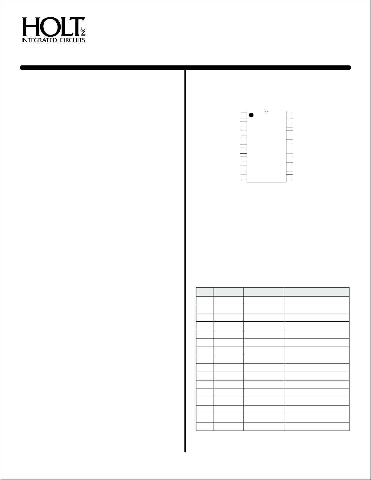
PINCONFIGURATION
V+
TESTB
ROUTB
ROUTA
TXBOUT
TXAOUT
N/C
1
2
3
4
5
6
7
V-
8
VCC
16
SLP1.5
15
TESTA
14
RINB
13
RINA
12
TX0IN
11
10
TX1IN
9
GND
SUPPLYVOLTAGES
Vcc=+5V±5%
V+=12Vto15V
V-=-12Vto-15V
PINDESCRIPTIONTABLE
PINSYMBOLFUNCTIONDESCRIPTION
FEATURES
! DirectARINC429interfacetolinedriver
andlinereceiver
!
Bothfunctionsinasingle16pinpackage
LineDriver
!
Internal
!
Digitaloutput
!
CMOS/TTLlogicpins
!
!
LineReceiver
Inputhystersisatleast2volts
!
Testinputsbypassanaloginputs
!
Outputtri-statemode
!
!
Plasticthermallyenhancedsurface
mount(ESOIC)package
Mil-temperaturerangeavailable
!
(DS8590Rev.B)01/01
zenersetsoutputlevels
slopecontrol
HOLTINTEGRATEDCIRCUITS
1
1V+POWER+12TO+15VOLTS
2TESTBLOGICINPUTCMOS
3ROUTBLOGICOUTPUTRECEIVERCMOSOUTPUTB
4ROUTALOGICOUTPUTRECEIVERCMOSOUTPUTA
5TXBOUTARINCOUTPUTLINEDRIVERTERMINALB
6TXAOUTARINCOUTPUTLINEDRIVERTERMINALA
7N/CNOCONNECT
8V-POWER-12TO-15VOLTS
9GNDPOWERGROUND
10TX1INLOGICINPUTCMOSORTTL
11TX0INLOGICINPUTCMOSORTTL
12RINAARINCINPUTRECEIVERAINPUT
13RINBARINCINPUTRECEIVERBINPUT
14TESTALOGICINPUTCMOS
15SLP1.5LOGICINPUTCMOSORTTL,V+ISOK
16VCCPOWER+5VOLTSUPPLY
FUNCTIONTABLES
HI-8590
LINEDRIVER
TX1IN TX0IN SLP1.5
TXAOUT TXBOUT
0 0 X 0V 0V
0 1 0 -5V 5V 10µs
0 1 1 -5V 5V 1.5µs
1 0 0 5V -5V 10µs
1 0 1 5V -5V 1.5µs
1 1 X 0V 0V
SLOPE
N /A
N /A
FUNCTIONALDESCRIPTION
LINEDRIVER
Figure1isablockdiagramofthelinedriver.The+5Vand
-5Vlevelsaregeneratedinternallyusingon-chipzeners.
Currentsforslopecontrolaresetbyzenervoltagesacross
on-chipresistors.
TheTX0INandTX1INinputsreceivelogicsignalsfroma
controltransmitterchipsuchastheHI-6010orHI-8282.
TXAOUTandTXBOUTholdeachsideoftheARINCbusat
GrounduntiloneoftheinputsbecomesaOne.IfforexampleTX1INgoeshigh,achargingpathisenabledto5Vonan
“A”sideinternalcapacitorwhilethe“B”sideisenabledto
-5V.ThechargingcurrentisselectedbytheSLP1.5pin.If
SLP1.5i shigh,thecapacitorisnominallychargedfrom
10%to90%in1.5µs.Iflow,theriseandfalltimesare10µs.
LINERECEIVER
RINA RINB TESTA TESTB ROUTA ROUTB
-1.25V to 1.25V -1.25V to 1.25V 0 0 0 0
-3.25V to -6.5V 3.25V to 6.5V 0 0 0 1
3.25V to 6.5V -3.25V to -6.5V 0 0 1 0
X X 0 1 0 1
X X 1 0 1 0
X X 1 1 HI-Z HI-Z
Aunitygainbufferreceivestheinternallygeneratedslopes
anddifferentiallydrivestheARINCline.Currentislimited
bytheseriesoutputresistorsateachpin.Thereareno
fusesinserieswiththeARINCoutputsoftheHI-8590as
existsontheHI-8382.
TheHI-8590has37.5ohmsinserieswitheachARINCoutputjustliketheHI-8585.TheHI-8586has10ohmsinseries.TheHI-8586isusedwiththeHI-8588forapplications
wheremoreseriesresistanceisaddedexternally,typically
forlightningprotectiondevices.
ThelinedriverinputsTX1IN,TX0IN,&SLP1.5mustbetied
toeitheralogi chighorlowifnotused.
ESD
PROTECTION
AND
VOLTAGE
TRANSLATION
ONE
NULL
ZERO
CONTROL
LOGIC
ONE
NULL
ZERO
CONTROL
LOGIC
5V
-5V
SLP1.5
5V
-5V
CURRENT
CONTROL
CURRENT
CONTROL
“A”SIDE
“B”SIDE
FIGURE1-LINEDRIVERBLOCKDIAGRAM
HOLTINTEGRATEDCIRCUITS
2
37.5OHMS
TXAOUT
TXBOUT
37.5OHMS

HI-8590
FUNCTIONALDESCRIPTION(cont.)
RECEIVER
Figure2showsthegeneralarchitectureoftheARINC429
receiver.ThereceiveroperatesofftheVCCsupplyonly.
TheinputsRINAandRINBeachhaveseriesresistors,typically35Kohms.Theyconnecttoleveltranslatorswhose
resistancetoGroundistypically10Kohms.Therefore,any
seriesresistanceaddedtotheinputswillaffectthevoltage
translation.
Afterleveltranslation,theinputsarebufferedandbecome
inputstoadifferentialamplifier.TheamplitudeofthedifferentialsignaliscomparedtolevelsderivedfromadividerbetweenVCCandGround.Thenominalsettingsc orrespondtoaOne/Zeroamplitudeof6.0VandaNullamplitudeof3.3V.
RINA
RINB
ESD
PROTECTION
AND
TRANSLATION
NULL
ZERO
ONE
NULL
ThestatusoftheARINCreceiverinputislatched.ANull
inputresetsthelatchesandaOneorZeroinputsetsthe
latches.
Thelogicattheoutputiscontrolledbythetestsignal
whichisgeneratedbythelogicalORoftheTESTAand
TESTBpins.Thereceiveroutputpinsfloatifboth
TESTAandTESTBarealogicOne.
TEST
S Q
LATCH
R
S Q
LATCH
R
TEST
TESTA
TEST
TEST
TESTB
TESTA'TESTB
TESTA'TESTB
ROUTA
ROUTB
FIGURE2-RECEIVERBLOCKDIAGRAM
APPLICATIONINFORMATION
Figure3showsapossibleapplicationofthe
HI-8590interfacingboththeARINCtransmit
andreceivechannelsofaHI-6010whichin
turninterfacestoan8-bitmicroprocessorbus.
HARDWIRE
OR
DRIVEFROMLOGIC
16
1
ì
í
î
14
2
15
12
13
6
5
9
4
3
11
10
8
FIGURE3-APPLICATIONDIAGRAM
HI-6010HI-8590
HOLTINTEGRATEDCIRCUITS
3
 Loading...