

January2001
HI-8588
DESCRIPTION
TheHI-8588isanARINC429businterfacereceiverandis
availableinaSO8pinpackage.Thetechnologyis
analog/digitalCMOS.Thecircuitryrequiresonlya5volt
supply.
TheARINCbuscanbeconnecteddirectlytothechip.The
typical10voltdifferentialsignalistranslatedandinputtoa
windowcomparatorandlatch.Thecomparatorlevelsare
justbelowthestandard6.5voltminimumARINCdata
thresholdandjustabovethestandard2.5voltmaximum
ARINCnullthreshold.
TheTESTAandTESTBinputsbypasstheanalogfor
testingpurposes.AlsoifTESTAandTESTBareboth
takenhigh,theanalog powersdownandthedigitaloutputs
tri-stateallowingwire-orpossibilities.
PleaserefertotheHI-8588-10forapplicationswherean
externalresistanceinserieswiththeARINCinputsis
requiredforlightningprotectionorwhenthedigitaloutputs
needtobealogiczeroratherthanopencircuitwhen
TESTAandTESTBarebothhigh.
PINCONFIGURATION
VCC
TESTA
2
3
RINB
4 5
RINA GND
81
7
6
SUPPLYVOLTAGES
vcc =5.0V±5%
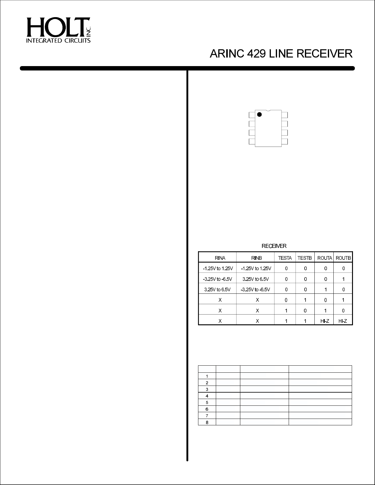
FUNCTIONTABLE
TESTB
ROUTB
ROUTA
FEATURES
!
DirectARINC429linereceiverinterface
inasmalloutlinepackage
!
Receiverinputhystersisatleast2volts
!
Testinputsthatbypassanaloginputand
canpowerdownandtri-stateoutputs
!
PlasticandceramicpackageoptionssurfacemountandDIP
!
Milprocessingavailable
PINDESCRIPTIONTABLE
PIN SYMBOL FUNCTION DESCRIPTION
VCC SUPPLY 5VOLTSUPPLY
TESTA LOGICINPUT CMOS
RINB ARINCINPUT RECEIVERBINPUT
RINA ARINCINPUT RECEIVERAINPUT
GND POWER GROUND
ROUTA LOGICOUTPUT RECEIVERCMOSOUTPUTA
ROUTB LOGICOUTPUT RECEIVERCMOSOUTPUTB
TESTB LOGICINPUT CMOS
HOLTINTEGRATEDCIRCUITS
(DS8588Rev.A)01/01
1
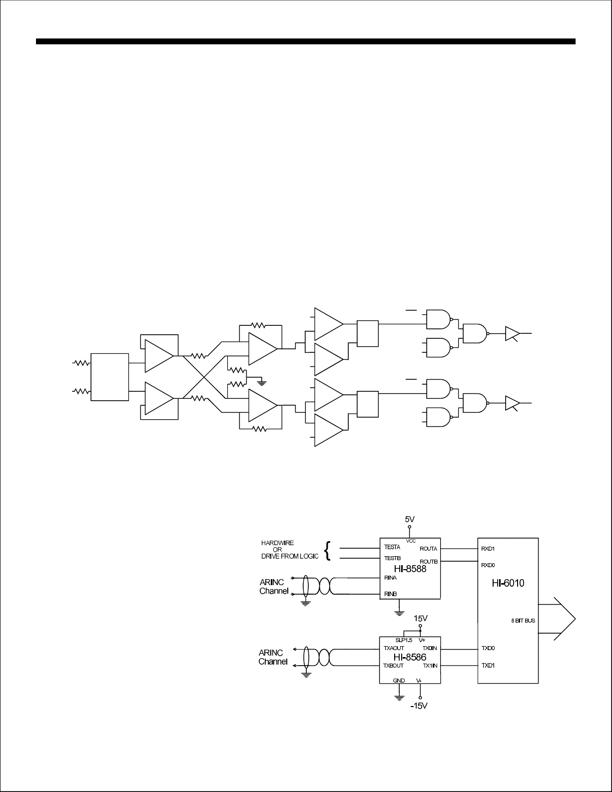
FUNCTIONALDESCRIPTION
RECEIVER
HI-8588
Figure1showsthegeneralarchitectureoftheARINC429
receiver.ThereceiveroperatesofftheVCCsupplyonly.
TheinputsRINAandRINBeachhaveseriesresistors,typically35Kohms.Theyconnecttoleveltranslatorswhose
resistancetoGroundistypically10Kohms.Therefore,any
seriesresistanceaddedtotheinputswillaffectthevoltage
translation.
Afterleveltranslation,theinputsarebufferedandbecome
inputstoadifferentialamplifier.TheamplitudeofthedifferentialsignaliscomparedtolevelsderivedfromadividerbetweenVCCandGround.Thenominals ettingscorrespondtoaOne/Zeroamplitudeof6.0VandaNullamplitudeof3.3V.
RINA
RINB
ESD
PROTECTION
AND
TRANSLATION
NULL
ZERO
ONE
NULL
ThestatusoftheARINCreceiverinputislatched.ANull
inputresetsthelatchesandaOneorZeroinputsetsthe
latches.
Thelogicattheoutputiscontrolledbythetestsignal
whichisgeneratedbythelogicalORoftheTestAand
TestBpins.IfTestAandTestBarebothOne,thenthereceiverispowereddownandtheoutputpinsfloat.The
powerdowndoesnotdisconnecttheinternalresistorsat
theARINCinput.
TEST
S Q
LATCH
R
S Q
LATCH
R
TEST
TESTA
TEST
TEST
TESTB
TESTA'TESTB
TESTA'TESTB
ROUTA
ROUTB
FIGURE1-RECEIVERBLOCKDIAGRAM
APPLICATIONINFORMATION
Figure2showsapossibleapplicationofthe
HI-8588interfacinganARINCreceivechannel
totheHI-6010whichinturninterfacestoan
8-bitbus.
1
2
8
4
3
5
1
6
7
5
4
6
7
8
2
3
FIGURE2-APPLICATIONDIAGRAM
HOLTINTEGRATEDCIRCUITS
2
 Loading...