

HOLT HI-8588PST-10, HI-8588PSI-10, HI-8588PDT-10, HI-8588PDI-10, HI-8588CRT-10 Datasheet
...
HI-8588-10
January2001
DESCRIPTION
TheHI-8588-10ARINC429businterfacereceiverissimilartotheHI-8588withtheexceptionthatitallowsanexternal10KohmresistorinserieswitheachARINCinputwithoutaffectingtheARINCinputthresholds.Theproductis
especiallyusefulinapplicationswherelightningprotection
circuitryisalsorequired.Inaddition,thetestinputsforce
bothoftheoutputstozeroinsteadopencircuit.Theanalog/digitalCMOSproductrequiresonlya5voltsupplyand
isavailableinaSO8pinpackage.
EachsideoftheARINCbusbeconnectedthrougha
10Kohmseriesresistorinorderforthe chiptodetectthe
correctARINClevels.Thetypical10voltdifferentialsignal
istranslatedandinputtoawindowcomparatorandlatch.
Thecomparatorlevelsaresetsothatwiththeexternal
10Kohmresistorstheyarejustbelowthestandard6.5volt
minimumARINCdatathresholdandjustabovethestandard2.5voltmaximumARINCnullthreshold.
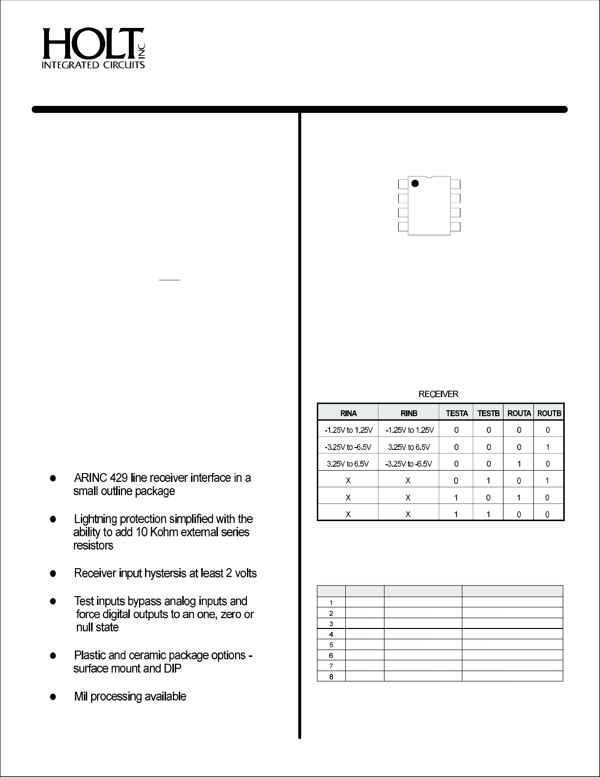
TheTESTAandTESTBinputsbypasstheanaloginputs
fortestingpurposes.AlsoifTESTAandTESTBareboth
takenhigh,thedigitaloutputsareforcedtozero.
must
ARINC429LINERECEIVER
PINCONFIGURATION
81
7
6
TESTB
ROUTB
ROUTA
VCC
TESTA
2
3
RINB
4 5
RINA GND
SUPPLYVOLTAGES
vcc =5.0V±5%
FUNCTIONTABLE
FEATURES
PINDESCRIPTIONTABLE
PIN SYMBOL FUNCTION DESCRIPTION
VCC SUPPLY 5VOLTSUPPLY
TESTA LOGICINPUT CMOS
RINB ARINCINPUT RECEIVERBINPUT
RINA ARINCINPUT RECEIVERAINPUT
GND POWER GROUND
ROUTA LOGICOUTPUT RECEIVERCMOSOUTPUTA
ROUTB LOGICOUTPUT RECEIVERCMOSOUTPUTB
TESTB LOGICINPUT CMOS
HOLTINTEGRATEDCIRCUITS
(DS8588-10Rev.A)01/01
1
FUNCTIONALDESCRIPTION
RECEIVER
HI-8588-10
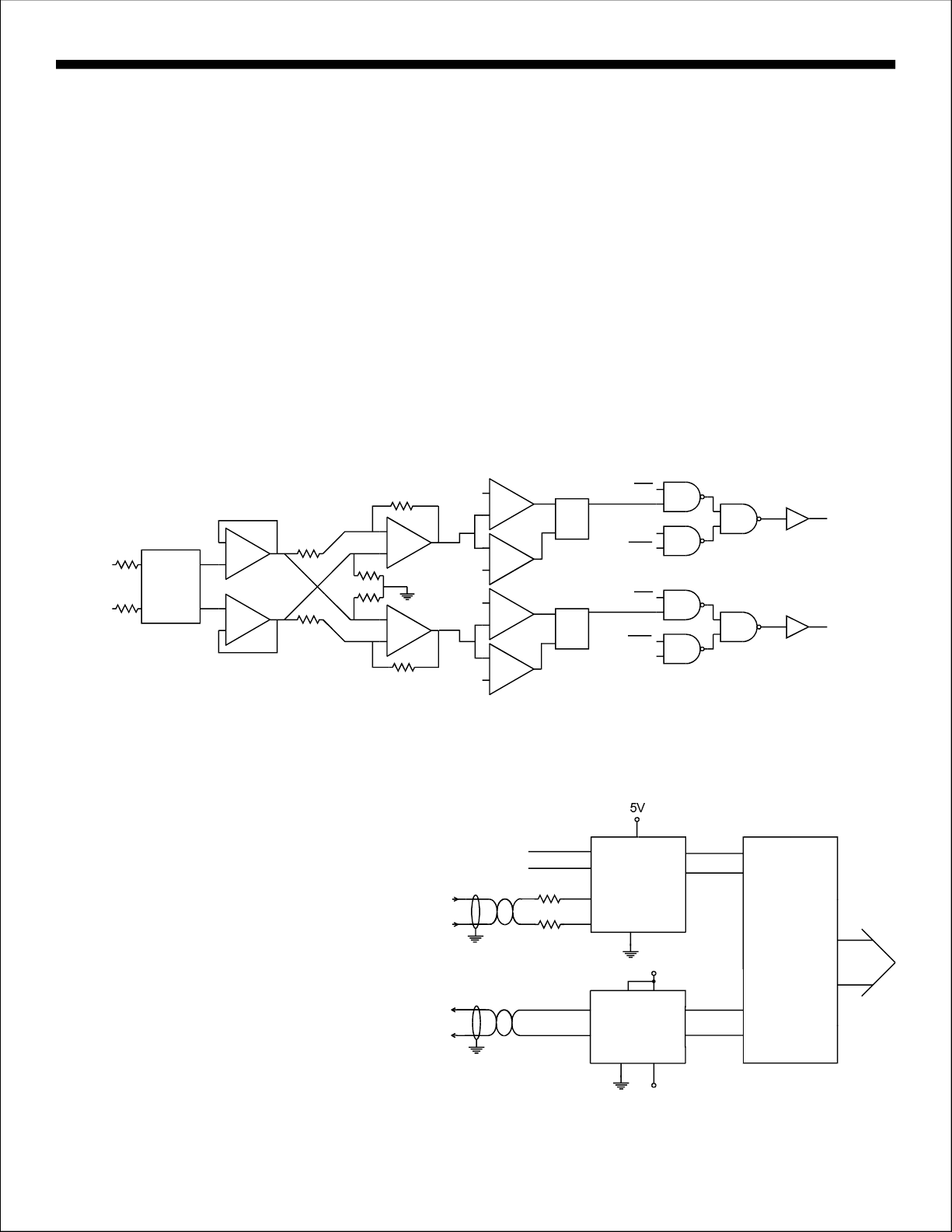
Figure1showsthegeneralarchitectureoftheARINC429
receiver.ThereceiveroperatesofftheVCCsupplyonly.
TheinputsRINAandRINBeachrequire35Kofresistanceofwhich25Kisinternaltothechip.Theseriesre-
W
W
sistanceisconnectedtoleveltranslatorswhoseresistance
toGroundistypically10K.Inorderforthevoltagetranslationnottobeadverselyaffected,anexternal10Kseries
W
W
resistermustbeaddedtoeachARINCinput.The
HI-8588-10deviceistypicallychosenforapplications
whereexternalseriesresistorsarerequiredinitslightning
protectioncircuit ry.
Afterleveltranslation,theinputsarebufferedandbecome
inputstoadifferentialamplifier.Theamplitudeofthedifferentialsignaliscomparedtolevelsderivedfromadivider
RINA
RINB
ESD
PROTECTION
AND
TRANSLATION
NULL
ZERO
NULL
ONE
betweenVCCandGround.ThenominalsettingscorrespondtoaOne/Zeroamplitudeof6.0VandaNullamplitudeof3.3V.
ThestatusoftheARINCreceiverinputislatched.ANull
inputresetsthelatchesandaOneorZeroinputsetsthe
latches.
Thelogicattheoutputiscontrolledbythetestsignal
whichisgeneratedbythelogicalORoftheTestAand
TestBpins.UnliketheHI-8588,ifTestAandTestBare
bothOne,theHI-8588-10outputsarepulledlowinstead
ofbeingtri-stated.Thisallowsthedigitaloutputsofa
transmittertobeconnectedtothetestinputsthrough
controllogicforself-testpurposes.
TEST
S Q
LATCH
R
S Q
LATCH
R
TESTA
TESTB
TEST
TESTA
TESTB
ROUTA
ROUTB
FIGURE1-RECEIVERBLOCKDIAGRAM
APPLICATIONINFORMATION
Figure2showsapossibleapplicationofthe
HI-8588interfacinganARINCreceivechannel
totheHI-6010whichinturninterfacestoan
8-bitbus.
HARDWIRE
OR
DRIVEFROMLOGIC
ARINC
Channel
ARINC
Channel
1
2
10K Ω
10K Ω
8
4
3
{
VCC
TESTA
TESTB
HI-8588-10
RINA
RINB
GND
5
ROUTA
ROUTB
6
7
15V
8
1
SLP1.5
V+
6
TXAOUT
HI-8586
7
TXBOUT
GND
5
4
-15V
2
TX0IN
3
TX1IN
V-
FIGURE2-APPLICATIONDIAGRAM
RXD1
RXD0
HI-6010
8BITBUS
TXD0
TXD1
HOLTINTEGRATEDCIRCUITS
2
 Loading...