

HI-8585,HI-8586
January2001
DESCRIPTION
TheHI-8585andHI-8586areCMOSintegratedcircuits
designedtodirectlydrivetheARINC429businan8pin
package.Twologicinputscontroladifferentialvoltage
betweentheoutputpinsproducinga+10voltOne,a
-10voltZero,anda0voltNull.
TheCMOS/TTLcontrolinputsaretranslatedtoARINC
specifiedamplitudesusingonboardzeners.Alogicinput
isprovidedtocontroltheslopeofthedifferentialoutput
signal.Timingissetbyon-chipresistorandcapacitorand
testedtobewithinARINCrequirements.
TheHI-8585has37.5ohmsinserieswitheachlinedriver
output.TheHI-8586pr ovidestheoptiontobypassmost
oftheoutputresistancesothatseriesprotectioncircuits
canaddtheirresistances.
TheHI-8585ortheHI-8586alongwiththeHI-8588line
receiverofferthesmallestoptionsavailabletogetonand
offtheARINCbus.
ARINC429LINEDRIVER
PINCONFIGURATION
SLP1.5
TX0IN
TX1IN
GND
1
2
3
4 5
SUPPLYVOLTAGES
V+=12Vto15V
V-=-12Vto-15V
FUNCTIONTABLE
8
7
6
V+
TXBOUT
TXAOUT
V-
FEATURES
! DirectARINC429linedriver
interfaceinasmallpackage
On-chipzenertosetoutputlevels
!
On-chiplinedriverslopecontroland
!
selectionbylogicinput
Lowcurrent12to15voltsupplies
!
CMOS/TTLlogicpins
!
Plasticandceramicpackageoptions-
!
surfacemountandDIP
!
ThemallyenhancedSOICpackages
!
Milprocessingavailable
TX1IN TX0IN SLP1.5
0 0 X 0V 0V
0 1 0 -5V 5V 10µs
0 1 1 -5V 5V 1.5µs
1 0 0 5V -5V 10µs
1 0 1 5V -5V 1.5µs
1 1 X 0V 0V
TXAOUT TXBOUT
PINDESCRIPTIONTABLE
SYMBOL FUNCTION DESCRIPTION
PIN
1 SLP1.5 LOGIC INPUT CMOS OR TTL, V+ IS OK
2 TX0IN LOGIC INPUT CMOS OR TTL
3 TX1IN LOGIC INPUT CMOS OR TTL
4 GND POWER GROUND
5 V- POWER -12 TO -15 VOLTS
6 TXAOUT LOGIC OUTPUT LINE DRIVER TERMINAL A
7 TXBOUT LOGIC OUTPUT LINE DRIVER TERMINAL B
8 V+ POWER +12 TO +15 VOLTS
SLOPE
N /A
N /A
HOLTINTEGRATEDCIRCUITS
(DS8585Rev.D)01/01
1
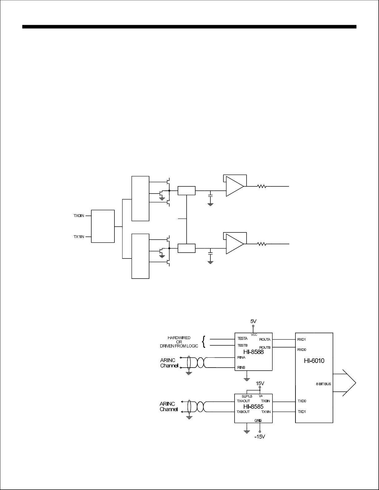
FUNCTIONALDESCRIPTION
HI-8585,HI-8586
Figure1isablockdiagramofthelinedriver.The+5Vand
-5Vlevelsaregeneratedinternallyusingon-chipzeners.
Currentsforslopecontrolaresetbyzenervoltagesacross
on-chipresistors.
TheTX0INandTX1INinputsreceivelogicsignalsfroma
controltransmitterchipsuchastheHI-6010orHI-8282.
TXAOUTandTXBOUTholdeachsideoftheARINCbusat
GrounduntiloneoftheinputsbecomesaOne.IfforexampleTX1INgoeshigh,achargingpathisenabledto5Vonan
“A”sideinternalcapacitorwhilethe“B”sideisenabledto
-5V.ThechargingcurrentisselectedbytheSLP1.5pin.If
theSLP1 .5pinishigh,thecapacitorisnominallycharged
from10%to90%in1.5µs.IfSLP1.5islow,theriseandfall
timesare10µs.
5V
ONE
NULL
ESD
PROTECTION
AND
VOLTAGE
TRANSLATION
ZERO
CONTROL
LOGIC
ONE
NULL
ZERO
CONTROL
LOGIC
-5V
SLP1.5
5V
-5V
Aunitygainbufferreceivestheinternallygeneratedslopes
anddifferentiallydrivestheARINCline.Currentislimited
bytheseriesoutputresistorsateachpin.Thereareno
fusesattheoutputsoftheHI-8585asexistsontheHI-8382.
TheHI-8585has37.5ohmsinserieswitheachoutput.The
HI-8586has10ohmsinseries.TheHI-8586isforapplicationswheremoreseriesresistanceisaddedexternally,
typicallyforlightningprotectiondevices.
“A”SIDE
CURRENT
CONTROL
CURRENT
CONTROL
“B”SIDE
HI-8585=37.5OHMS
HI-8556=10.0OHMS
HI-8585=37.5OHMS
HI-8586=10.0OHMS
TXAOUT
TXBOUT
APPLICATIONINFORMATION
Figure2showsapossibleapplication
oftheHI-8585/86interfacinganARINC
transmitchannelfromtheHI-6010.
FIGURE1-LINEDRIVERBLOCKDIAGRAM
2
8
4
3
5
1
6
7
4 5
FIGURE2-APPLICATIONDIAGRAM
1
6
7
8
2
3
HOLTINTEGRATEDCIRCUITS
2
HI-8585,HI-8586
ABSOLUTEMAXIMUMRATINGS
VoltagesreferencedtoGround
RECOMMENDEDOPERATINGCONDITIONS
SupplyVoltages
V+....................+12V±5%or+15V±10%
Supplyvoltages
V-.....................-12V±5%or-15V±10%
V+....................................................20V
V-....................................................-20V
TemperatureRange
IndustrialScreening.........-40°Cto+85°C
DCcurrentperinputpin................+10mA
Hi-TempScreening........-55°Cto+125°C
MilitaryScreening..........-55°Cto+125°C
Powerdissipationat25°C
plasticDIL............1.0W,derate10mW/°C
ceramicDIL..........0.5W,derate7mW/°C
NOTE:Stressesaboveabsolutemaximum
SolderTemperature........275°Cfor10sec
ratingsoroutsiderecommendedoperating
conditionsmaycausepermanentdamageto
StorageTemperature........-65°Cto+150°C
thedevice.Thesearestressratingsonly.
Operationatthelimitsisnotrecommended.
DCELECTRICALCHARACTERISTICS
V+=+12Vto+15V,V-=-12Vto-15V,T=OperatingTemperatureRange(unlessotherwisestated)
PARAMETERSSYMBOLTESTCONDITIONSMINTYPMAXUNITS
Inputvoltage(TX1IN,TX0IN,SLP1.5)
highV2.1-V+volts
lowV--0.5volts
A
IH
IL
Inputcurrent(TX1IN,TX0IN,SLP1.5)
sourceIV=0V--0.1A
sinkIV=5V--0.1A
IHIN
ILIN
ARINCoutputvoltage(Differential)
oneVnoload;TXAOUT-TXBOUT9.0010.0011.00volts
zeroVnoload-11.00-10.00-9.00volts
nullVnoload-0.5000.50volts
DIFF1
DIFF0
DIFFN
;TXAOUT-TXBOUT
;TXAOUT-TXBOUT
ARINCoutputvoltage(Ref.toGND)
oneorzeroVnoload&magnitudeatpin4.505.005.50volts
nullVnoload-0.2500.25volts
Operatingsupplycurrent
V+I-6.014.0mA
V-I-14.0-6.0-mA
ARINCoutputimpedenceZNote1
DOUT
NOUT
DD
EE
OUT
SLP1.5=V+
TX1IN&TX0IN=0V:noload
IN&TX1IN=0V:noloadTX0
HI-8585-37.5-ohms
HI-8586-10-ohms
NOTE:
1.TheoutputresistanceischeckedbymeasuringthemomentaryshortcircuitcurrentateachARINCoutputpin.
µ
µ
HOLTINTEGRATEDCIRCUITS
3
 Loading...