

HI-8582,HI-8583
June2001
GENERALDESCRIPTION
TheHI-8582fromHoltIntegratedCircuitsisasilicongate
CMOSdeviceforinterfacinga16-bitparalleldatabus
directlytotheARINC429serialbus.TheHI-8582design
offersmanyenhancementstotheindustrystandardHI8282architecture.Thedeviceprovidestworeceiverseach
withlabelrecognition,32by32FIFO,andanalogline
receiver.Upto16labelsmaybeprogrammedforeach
receiver.Theindependenttransmitterhasa32by32FIFO
andabuilt-inlinedriver.ThestatusofallthreeFIFOscan
bemonitoredusingtheexternalstatuspins,orbypolling
theHI-8582’sstatusregister.Othernewfeaturesincludea
programmableoptionofdataorparityinthe32ndbit,and
theabilitytounscramblethe32bitword.Also,versions
areavailablewithdifferentvaluesofinputresistanceand
outputresistancetoallowuserstomoreeasilyaddexternal
lightningprotectioncircuitry.Thedevicecanbeusedat
nonstandarddatarateswhenanoptionpin,,is
invoked.
NFD
ARINC429SystemonaChip
FEATURES
!
ARINCspecification429compatible
!
Dualreceiverandtransmitterinterface
!
Analoglinedriverandreceiversconnect
directlytoARINCbus
!
Programmablelabelrecognition
!
On-chip16labelmemoryforeachreceiver
!
32x32FIFOseachreceiverandtransmitter
!
Independentdatarateselectionfor
transmitterandeachreceiver
!
Statusregister
!
Datascramblecontrol
!
32ndtransmitbitcanbedataorparity
!
Selftestmode
!
Lowpower
The16-bitparalleldatabusexchangesthe32-bitARINC
datawordintwostepswheneitherloadingthetransmitter
orinterrogatingthereceivers.Thedatabus,andallcontrol
signalsareCMOSandTTLcompatible.
TheHI-8582appliestheARINCprotocoltothereceivers
andtransmitter.Timingisbasedona1Megahertzclock.
Althoughthelinedriversharesacommonsubstratewith
thereceivers,thedesignofthephysicalisolationdoesnot
allowparasiticcrosstalk,andtherebyachievesthesame
isolationascommonhybridlayouts.
APPLICATIONS
!
Avionicsdatacommunication
!
Serialtoparallelconversion
!
Paralleltoserialconversion
!
Industrial&fullmilitarytemperatureranges
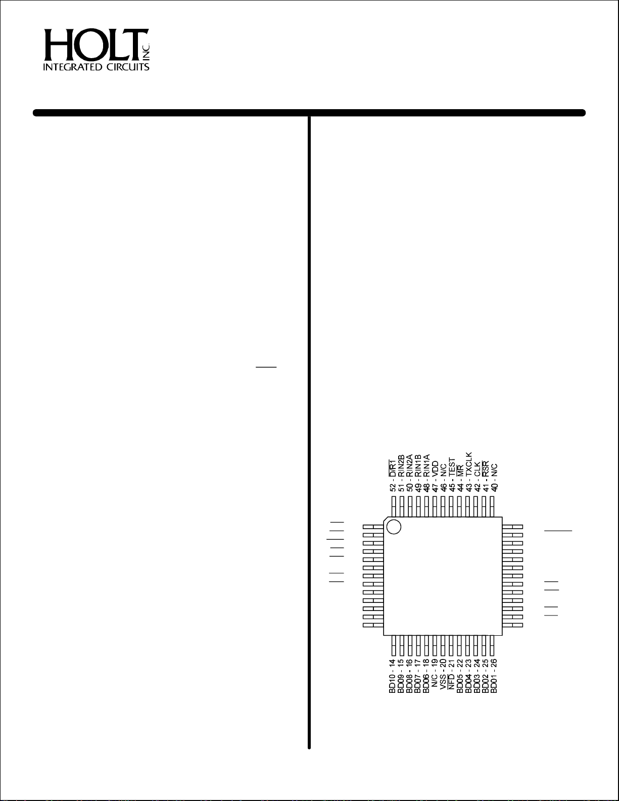
PINCONFIGURATION (TopView)
FF1
-1
HF1
-2
D/R2
-3
FF2
-4
HF2
-5
SEL-6
EN1
-7
EN2
-8
BD15-9
BD14-10
BD13-11
BD12-12
BD11-13
HI-8582PQI
&
HI-8582PQT
39-N/C
38-
CWSTR
37-ENTX
36-V+
35-TXBOUT
34-TXAOUT
33-V32-
FFT
31-
HFT
30-TX/R
29-
PL2
28-
PL1
27-BD00
52-PinPlasticQuadFlatPack(PQFP)
(Seepage14foradditionalpinconfiguration)
HOLTINTEGRATEDCIRCUITS
1(DS8582Rev.H)06/01
PINDESCRIPTIONS
SIGNALFUNCTIONDESCRIPTION
VDDPOWER+5V±%
RIN1AINPUTARINCreceiver1positiveinput
RIN1BINPUTARINCreceiver1negativeinput
RIN2AINPUTARINCreceiver2positiveinput
RIN2BINPUTARINCreceiver2negativeinput
D/R1
FF1
HF1
D/R2
FF2
HF2
SELINPUTReceiverdatabyteselection(0=BYTE1)(1=BYTE2)
EN1
EN2EN1
BD15I/ODataBus
BD14I/ODataBus
BD13I/ODataBus
BD12I/ODataBus
BD11I/ODataBus
BD10I/ODataBus
BD09I/ODataBus
BD08I/ODataBus
BD07I/ODataBus
BD06I/ODataBus
GNDPOWER0V
BD05I/ODataBus
BD04I/ODataBus
BD03I/ODataBus
BD02I/ODataBus
BD01I/ODataBus
BD00I/ODataBus
PL1
PL2PL1.
TX/ROUTPUTTransmitterreadyflag.GoeslowwhenARINCwordloadedintoFIFO.Goeshigh
HFT
FFT
V-POWER-9.5Vto-12.6V
TXAOUTOUTPUTLinedriveroutput-Aside
TXBOUTOUTPUTLine driveroutput-Bside
V+POWER+9.5Vto+12.6V
ENTXINPUTEnableTransmission
CWSTR
RSR
NFD
CLKINPUTMasterClockinput
TXCLKOUTPUTTransmitterClockequaltoMasterClock(CLK),dividedbyeither10or80.
MR
TESTINPUTDisableTransmitteroutputifhigh(pull-down)
OUTPUTReceiver1datareadyflag
OUTPUTFIFOfullReceiver1
OUTPUTFIFOHalffull,Receiver1
OUTPUTReceiver2datareadyflag
OUTPUTFIFOfullReceiver2
OUTPUTFIFOHalffull,Receiver2
INPUTDataBuscontrol,enablesreceiver1datatooutputs
INPUTDataBuscontrol,enablesreceiver2datatooutputsifishigh
INPUTLatchenableforbyte1enteredfromdatabustotransmitterFIFO.
INPUTLatchenableforbyte2enteredfromdatabustotransmitterFIFO.Mustfollow
OUTPUTTransmitterFIFOHalfFull
OUTPUTTransmitterFIFOFull
INPUTClockforcontrolwordregister
INPUTReadStatusRegisterifSEL=0,readControlRegisterifSEL=1
INPUTNofrequencydiscriminationiflow(pull-up)
INPUTMasterReset,activelow
HI-8582,HI-8583
5
aftertransmissionandFIFOempty.
HOLTINTEGRATEDCIRCUITS
2
FUNCTIONALDESCRIPTION
CONTROLWORDREGISTER
HI-8582,HI-8583
STATUSREGISTER
TheHI-8582containsa16-bitcontrolregisterwhichisusedto
configurethedevice.ThecontrolregisterbitsCR0-CR15are
loadedfromBD00-BD15whenispulsedlow.Thecontrol
registercontentsareoutputonthedatabuswhenSEL=1and
CWSTR
RSR
ispulsedlow.Eachbitofthecontrolregisterhasthefollowing
function:
CR
BitFUNCTIONSTATEDESCRIPTION
CR0Receiver10Datarate=CLK/10
CR1LabelMemory0Normaloperation
CR2EnableLabel0Disablelabelrecognition
CR3EnableLabel0DisableLabelRecognition
CR4Enable0Transmitter32ndbitisdata
CR5SelfTest0Aninternalconnectionismade
CR6Receiver10Receiver1decoderdisabled
CR7--Ifreceiver1decoderisenabled,
CR8--Ifreceiver1decoderisenabled,
CR9Receiver20Receiver2decoderdisabled
CR10--Ifreceiver2decoderisenabled,
CR11--Ifreceiver2decoderisenabled,
CR12Invert0Transmitter32ndbitisOddparity
CR13Transmitter0Datarate=CLK/10,O/Pslope=1.5us
CR14Receiver20Datarate=CLK/10
Dataclock
select1Datarate=CLK/80
Read/Write
Recognition
(Receiver1)1Enablelabelrecognition
Recognition
(Receiver2)1EnableLabelrecognition
32ndbit
asparity1Transmitter32ndbitisparity
decoder
Decoder
Transmitter
parity1Transmitter32ndbitisEvenparity
dataclock
select1Datarate=CLK/80,O/Pslope=10us
dataclock
select1Datarate=CLK/80
1Load16labelsusing/
Read16labelsusing/
passingTXAOUTandTXBOUT
tothereceiverinputs
1Normaloperation
1ARINCbits9and10mustmatch
CR7andCR8
theARINCbit9mustmatchthisbit
theARINCbit10mustmatchthisbit
1ARINCbits9and10mustmatch
CR10andCR11
theARINCbit9mustmatchthisbit
theARINCbit10mustmatchthisbit
PL1PL2
EN1EN2
TheHI-8582containsa9-bitstatusregisterwhichcanbe
interrogatedtodeterminethestatusoftheARINCreceivers,data
FIFOsandtransmitter.Thecontentsofthestatusregisterareoutput
onBD00-BD08whenthepinistakenlowandSEL=0.Unused
RSR
bitsareoutputaszeros.Thefollowingtabledefinesthestatus
registerbits.
SR
BitFUNCTIONSTATEDESCRIPTION
SR0Dataready0Receiver1FIFOempty
(Receiver1)
SR1FIFOhalffull0Receiver1FIFOholdslessthan16
(Receiver1)words
SR2FIFOfull0Receiver1FIFOnotfull
(Receiver1)
SR3Dataready0Receiver2FIFOempty
(Receiver2)
SR4FIFOhalffull0Receiver2FIFOholdslessthan16
(Receiver2)words
SR5FIFOfull0Receiver2FIFOnotfull
(Receiver2)
SR6TransmitterFIFO0TransmitterFIFOnotempty
empty
SR7TransmitterFIFO0TransmitterFIFOnotfull
full
SR8TransmitterFIFO0TransmitterFIFOcontainslessthan
halffull16words
1Receiver1FIFOcontainsvaliddata
Resetstozerowhenalldatahas
beenread.pinistheinverseof
thisbit
1Receiver1FIFOholdsatleast16
words.pinistheinverseof
thisbit.
1Receiver1FIFOfull.Toavoiddata
loss,theFIFOmustbereadwithin
oneARINCwordperiod.pinis
theinverseofthisbit
1Receiver2FIFOcontainsvaliddata
Resetstozerowhenalldatahas
beenread.pinistheinverseof
thisbit
1Receiver2FIFOholdsatleast16
words. pinistheinverseof
thisbit.
1Receiver2FIFOfull.Toavoiddata
loss,theFIFOmustbereadwithin
oneARINCwordperiod.pinis
theinverseofthisbit
1TransmitterFIFOempty.
1TransmitterFIFOfull.pinisthe
inverseofthisbit.
1TransmitterFIFOcontainsatleast
16words.pinisthe
inverseofthisbit.
D/R1
HF1
FF1
D/R2
HF2
FF2
FFT
HFT
CR15Data0ScrambleARINCdata
format
1UnscrambleARINCdata
HOLTINTEGRATEDCIRCUITS
3
HI-8582,HI-8583
FUNCTIONALDESCRIPTION(cont.)
ARINC429DATAFORMAT
ControlregisterbitCR15isusedtocontrolhowindividualbitsinthe
receivedortransmittedARINCwordaremappedtotheHI-8582data
busduringdatareadorwriteoperations.Thefollowingtable
describesthismapping:
BYTE1
DATABDBDBDBDBDBDBDBDBDBDBDBDBDBDBDBD
BUS15141312111009080706050403020100
ARINC13121110931303212345678
BIT
CR15=0
ARINC16151413121110987654321
BIT
CR15=1
BYTE2
DATABDBDBDBDBDBDBDBDBDBDBDBDBDBDBDBD
BUS15141312111009080706050403020100
ARINC29282726252423222120191817161514
BIT
CR15=0
ARINC32313029282726252423222120191817
CR15=1
TheHI-8582guaranteesrecognitionoftheselevelswithacommon
modeVoltagewithrespecttoGNDlessthan±5Vfortheworstcase
condition(4.75Vsupplyand13Vsignallevel).
Thetolerancesinthedesignguaranteedetectionoftheabove
levels,sotheactualacceptancerangesareslightlylarger.Ifthe
ARINCsignalisoutoftheactualacceptanceranges,includingthe
nulls,thechiprejectsthedata.
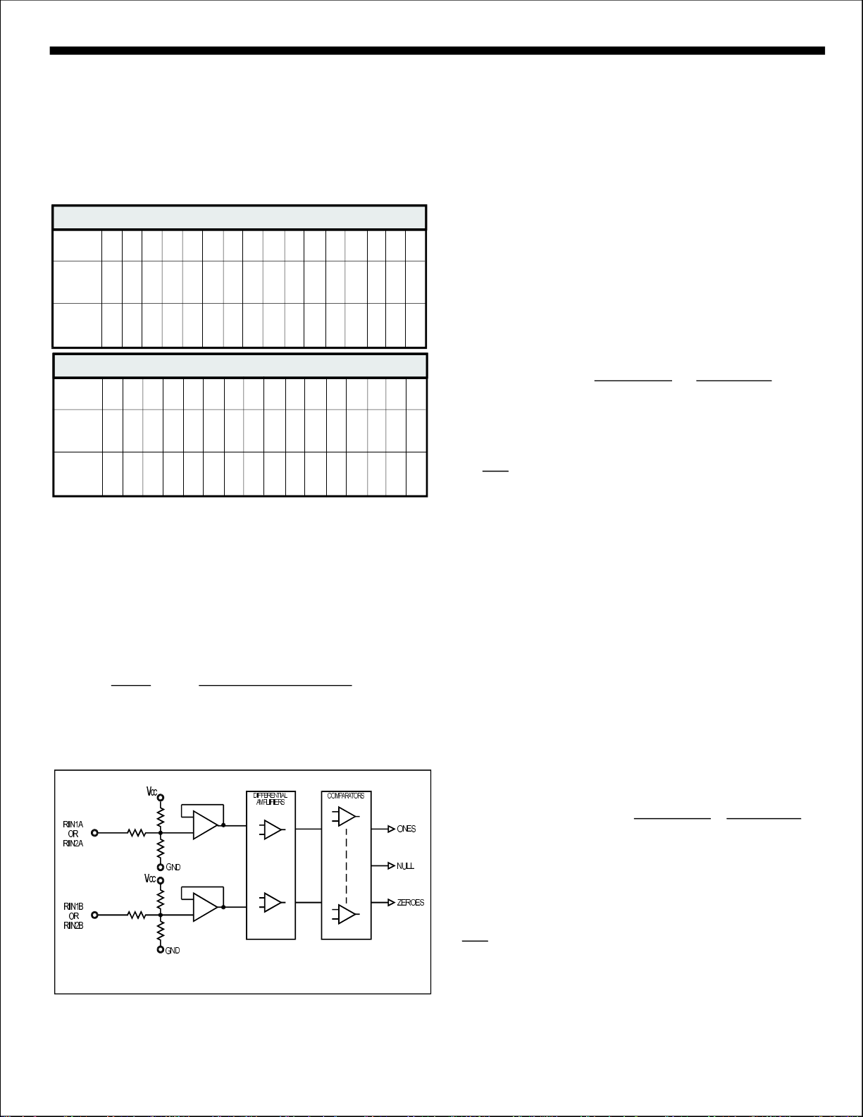
RECEIVERLOGICOPERATION
Figure2showsablockdiagramofthelogicsectionofeachreceiver.
BITTIMING
TheARINC429specificationcontainsthefollowingtimingspecificationforthereceiveddata:
HIGHSPEEDLOWSPEED
BITRATE
PULSERISETIME
PULSEFALLTIME
PULSEWIDTH
Ifthepinishigh,theHI-8582acceptssignalsthatmeetthese
NFD
100KBPS±1%12K-14.5KBPS
1.5±0.5µsec10±5µsec
1.5±0.5µsec10±5µsec
5µsec±5%34.5to41.7µsec
specificationsandrejectsoutsidethetolerances.Thewaythelogic
operationachievesthisisdescribedbelow:
THERECEIVERS
ARINCBUSINTERFACE
Figure1showstheinputcircuitforeachreceiver.TheARINC429
specificationrequiresthefollowingdetectionlevels:
STATEDIFFERENTIALVOLTAGE
ONE+6.5Voltsto+13Volts
NULL+2.5Voltsto-2.5Volts
ZERO-6.5Voltsto-13Volts
FIGURE1.ARINCRECEIVERINPUT
1.Keytotheperformanceofthetimingcheckinglogicisanaccurate1MHzclocksource.Lessthan0.1%errorisrecommended.
2.Thesamplingshiftregistersare10bitslongandmustshow
threeconsecutiveOnes,ZerosorNullstobeconsideredvalid
data.Additionally,fordatabits,theOneorZerointheupper
bitsofthesamplingshiftregistersmustbefollowedbyaNullin
thelowerbitswithinthedatabittime.ForaNullinthewordgap,
threeconsecutiveNullsmustbefoundinboththeupperand
lowerbitsofthesamplingshiftregister.Inthismannertheminimumpulsewidthisguaranteed.
3.Eachdatabitmustfollowitspredecessorbynotlessthan8
samplesandnomorethan12samples.Inthismannerthebit
rateischecked.Withexactly1MHzinputclockfrequency,the
acceptabledatabitratesareasfollows:
HIGHSPEEDLOWSPEED
DATABITRATEMIN
DATABITRATEMAX
83KBPS10.4KBPS
125KBPS15.6KBPS
4.TheWordGaptimersamplestheNullshiftregisterevery10
inputclocks(80forlowspeed)afterthelastdatabitofavalid
reception.IftheNullispresent,theWordGapcounteris
incremented.Acountof3willenablethenextreception.
Ifisheldlow,frequencydiscriminationisdisabledandany
NFD
datastreamtotaling32bitsisacceptedevenwithgapsbetween
bits.Theprotocolstillrequiresawordgapasdefinedin4.above.
HOLTINTEGRATEDCIRCUITS
4

HI-8582,HI-8583
FUNCTIONALDESCRIPTION(cont.)
RECEIVERPARITY
Thereceiverparitycircuitcountsonesreceived,includingthe
paritybit.Iftheresultisodd,then"0"willappearinthe32ndbit.
RETRIEVINGDATA
Once32validbitsarerecognized,thereceiverlogicgeneratesan
EndofSequence(EOS).Dependinguponthestateofcontrol
registerbitsCR2-CR11,thereceivedARINC32-bitwordisthen
checkedforcorrectdecodingandlabelmatchingbeforebeing
loadedintothe32x32receiveFIFO.ARINCwordswhichdonot
meetthenecessary9thand10thARINCbitorlabelmatchingare
ignoredandarenotloadedintothereceiveFIFO.Thefollowing
tabledescribesthisoperation.
TOPINS
SEL
EN
HF
FF
D/R
MUX
CONTROL
FIFO
LOAD
CONTROL
32TO16DRIVER
32X32
FIFO
CR2(3)ARINCwordCR6(9)ARINCwordFIFO
matchesbits9,10
labelmatch
CR7,8(10,11)
0X0XLoadFIFO
1No0XIgnoredata
1Yes0XLoadFIFO
0X1NoIgnoredata
0X1YesLoadFIFO
1Yes1NoIgnoredata
1No1YesIgnoredata
1No1NoIgnoredata
1Yes1YesLoadFIFO
R/W
CONTROL
CONTROL
BITS
CONTROL
BIT
ONES
NULL
ZEROS
16x8
LABEL
MEMORY
EOS
LABEL/
DECODE
/
COMPARE
SHIFTREGISTER
SHIFTREGISTER
SHIFTREGISTER
FIGURE2. RECEIVERBLOCKDIAGRAM
32BITSHIFTREGISTER
CONTROLBITS
DATA
BITCLOCK
WORDGAP
START
CR0,CR14
PARITY
CHECK
WORDGAP
SEQUENCE
CONTROL
DETECTION
TIMER
ERROR
32ND
BIT
CLOCK
OPTION
BIT
COUNTER
AND
ENDOF
SEQUENCE
BITCLOCK
END
ERROR
CLOCK
CLK
CLOCK
HOLTINTEGRATEDCIRCUITS
5
 Loading...