

February2001
GENERALDESCRIPTION
TheHI-8482businterfaceunitisasilicongateCMOSdevicedesignedasadualdifferentiallinereceiverinaccordancewiththerequirementsoftheARINC429busspecification.ThedevicetranslatesincomingARINC429signalstonormalCMOS/TTLlevelsoneachofitstwoindependentreceivechannels.TheHI-8482isalsofunctionallyequivalenttotheFairchild/RaytheonRM3183.
Theself-testinputsforcetheoutputstoeitheraZERO,
ONE,orNULLstateforsystemtests.Whileinself-test
mode,theARINCinputsareignored.
AlltheARINCinputshavebuilt-inhysteresistoreject
n oisethatmaybepresentontheARINCbus.Additional
inputnoisefilteringcanalsobeaccomplishedwithexternalcapacitors.
TheHI-8482linereceiverisoneofseveraloptionsofferedbyHoltIntegratedCircuitstointerfacetotheARINC
bus.Thedigitaldataprocessingforserial-to-parallelconversionandclockrecoverycanbeaccomplishedwiththe
HI-6010,HI-8683orsimilardevices.
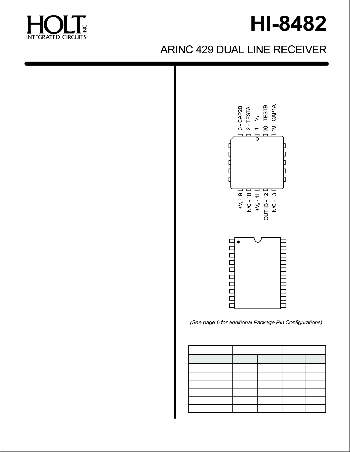
TheHI-8482isavailableinavarietyofceramic&plastic
packagesincludingSmallOutline(SOIC),
Cerquad,
DIP&LeadlessChipCarrier(LCC).
J-LeadPLCC,
FEATURES
PINCONFIGURATIONS (TopViews)
IN2B-4
OUT2B-5
IN2A-6
CAP2A-7
OUT2A-8
-V-1
S
TESTA-2
CAP2B-3
IN2B-4
OUT2B-5
IN2A-6
CAP2A-7
OUT2A-8
+V-9
L
N/C-10
HI-8482J
HI-8482JT
20-PIN
PLASTIC
J-LEADPLCC
HI-8482PSI
HI-8482PST
20-PIN
PLASTIC
SMALL
OUTLINE
(SOIC)-WB
18-IN1A
17-CAP1B
16-IN1B
15-OUT1A
14-GND
20-TESTB
19-CAP1A
18-IN1A
17-CAP1B
16-IN1B
15-OUT1A
14-GND
13-N/C
12-OUT1B
11-+V S
!
ConvertsARINC429levelstodigitaldata
!
DirectreplacementfortheRM3183
!
Greaterthan2voltreceivinghysteresis
!
TTLandCMOSoutputsandtestinputs
!
Militaryscreeningavailable
!
20-PinSOIC,PLCC,CERQUAD.DIP&
LCCpackagesareavailable
HOLTINTEGRATEDCIRCUITS
TRUTHTABLE
ARINCINPUTSTESTINPUTSOUTPUTS
V(A)-V(B)TESTATESTBOUTAOUTB
Null0000
Zero0001
One0010
Don'tCare0101
Don'tCare1010
Don'tCare1100
1(DS8482Rev.C)02/01
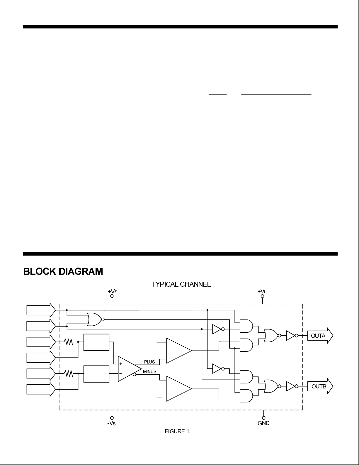
FUNCTIONALDESCRIPTION
HI-8482
TheHI-8482containstwoindependentARINC429receive
channels.ThediagraminFigure1illustratesatypicalHI8482receivechannel.
ThedifferentialARINCsignalinputisconvertedtoapositive
signalreferencedtogroundthroughlevelshiftersanda
unitygaindifferentialamplifier.
Apositivedifferentialinputsignalisconvertedtoapositive
signalontheplusoutputofthedifferentialamplifier.This
outputisproportionalinamplitudetotheoriginalinput
signal.Atthesametime,thecorrespondingMINUSoutput
ispulledtoGND.Likewisewhenanegativeinputsignalis
p resentattheARINCinputs,apositivesignalispresenton
theMINUSoutputandthePLUSoutputispulledtoGND.
Theoutputsofthedifferentialamplifierarecomparedwith
theONE,ZEROandNULLthresholdlevelstoproducethe
appropriatelogiclevelontheOUTAandOUTBoutputsof
thedevice.TheARINCclocksignalmayberecovered
throughaNORfunctionofOUTAandOUTB.
Thetestinputslogicallydisconnecttheoutputsofthe
comparatorsfromOUTAandOUTBandforcethedevice
outputstooneofthethreevalidstates(Figure5).This
alleviateshavingtogroundtheARINCinputsduringtest
mode operation.
ARINCLEVELS
TheARINC429specificationrequiresthefollowing
detectionlevels:
STATEDIFFERENTIALVOLTAGE
ONE+6.5Vto+13V
NULL+2.5Vto-2.5V
ZERO-6.5Vto-13V
TheHI-8482guaranteesrecognitionoftheselevelswitha
commonmodevoltagewithrespecttoGNDlessthan
±5Vfortheworstcasecondition.
NOISE
Theinputhysteresisissettorejectvoltageleveltransitions
intheundefinedregionbetweenthemaximumZEROlevel
andtheminimumNULLlevelandtheundefinedregion
betweenthemaximumNULLlevelandtheminimumONE
level.Therefore,onceavalidinputdifferentialvoltage
thresholdisdetected,theoutputswillremainatavalidlogic
stateuntilanewvalidinputvoltageisdetected.
Inadditiontothehysteresis,theCapAandCapBpinsmake
itpossibletoaddsimpleRCfilterstotheARINCinputs.
TESTA
TESTB
INA
CAPA
INB
CAPB
LEVEL
SHIFT
LEVEL
SHIFT
Detect
Level
Comp
DIFF
AMP
Detect
Level
Comparators
w/hysteresis
Comp
HOLTINTEGRATEDCIRCUITS
2
HI-8482
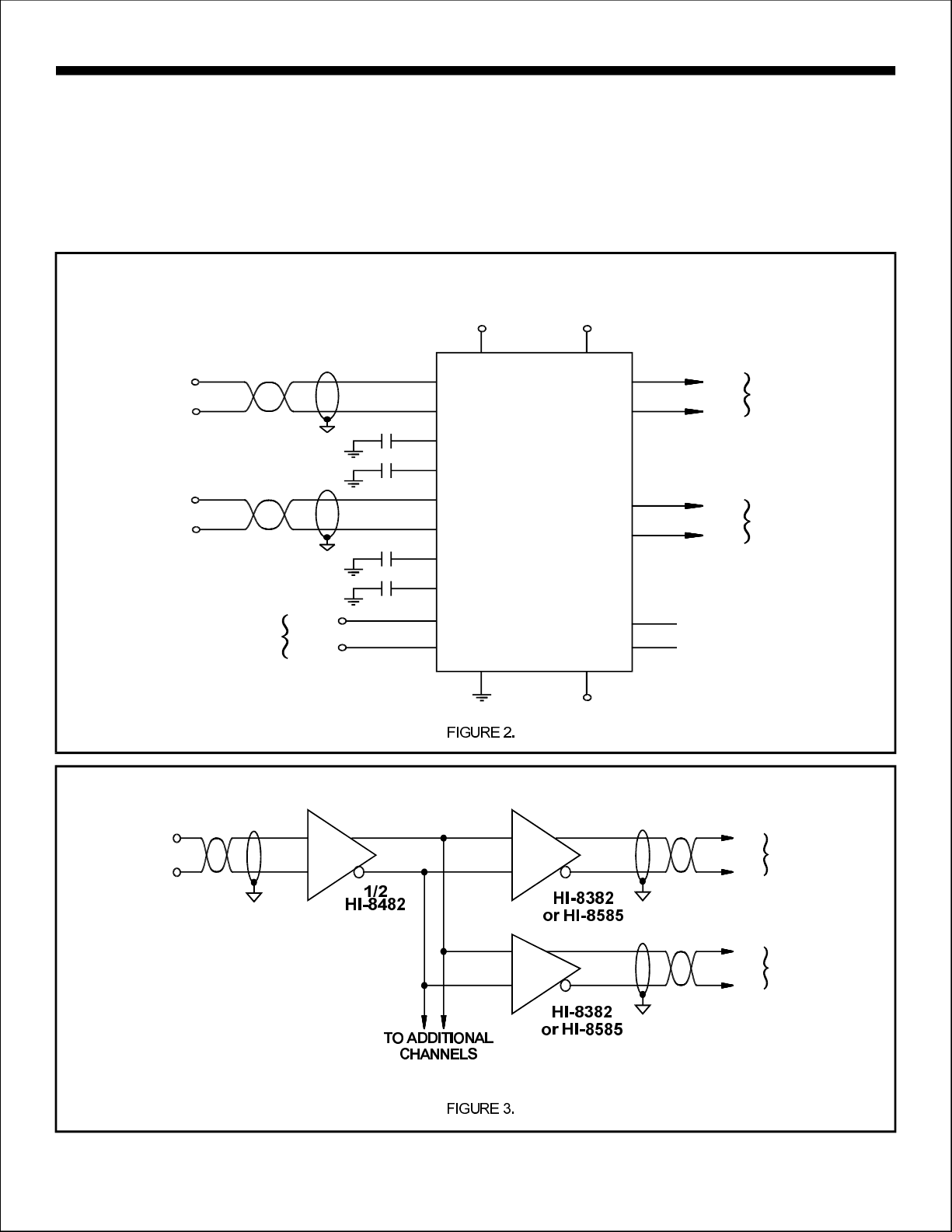
TYPICALAPPLICATIONS
APPLICATIONS
ThestandardconnectionsfortheHI-8482areshowninFigure2.
DecouplingofthesupplyshouldbedoneneartheICtoavoid
propagationofnoisespikesduetoswitchingtransients.The
ARINCRECEIVERSTANDARDCONNECTIONS
ARINC
CHANNEL1
39pF
39pF
ARINC
CHANNEL2
39pF
39pF
ground(GND)connectionshouldbesturdyandisolatedfromlarge
switchingcurrentstoprovideaquietgroundreference.
TheHI-8482canbeusedwithHI-8382orHI-8585LineDriversto
provideacompleteanalogARINC429interfacesolution.Asimple
application,whichcanbeusedinsystemsrequiringarepeater
typecircuitforlongtransmissionsorfortestinterfaces,isgivenin
Figure3.MoreHI-8382orHI-8585driversmaybeaddedtotest
multipleARINCchannels,asshown.
+5V
+15V
HI-8482
IN1A
IN1B
CAP1A
CAP1B
IN2A
IN2B
CAP2A
CAP2B
OUT1A
OUT1B
OUT2A
OUT2B
A
B
A
B
CHANNEL1
DATAOUT
TOLOGIC
CHANNEL2
DATAOUT
TOLOGIC
ARINC
INPUT
CHANNEL
LOGIC
TEST
INPUTS
IN1A
IN1B
TESTA
TESTB
ARINCREPEATERCIRCUIT
OUT1A
OUT1B
DATA(A)
DATA(B)
DATA(A)
DATA(B)
-15V
AOUT
BOUT
AOUT
BOUT
N/C
N/C
A
B
A
B
ARINC
OUTPUT
CHANNEL1
ARINC
OUTPUT
CHANNEL2
HOLTINTEGRATEDCIRCUITS
3

HI-8482
PINDESCRIPTIONTABLE
SYMBOLFUNCTIONDESCRIPTION SYMBOLFUNCTIONDESCRIPTION
CAP1AINPUTFiltercapacitorinputforterminalAof
channel1
CAP1BINPUTFiltercapacitorinputforterminalBof
channel1
CAP2AINPUTFiltercapacitorinputforterminalAof
channel2
CAP2BINPUTFiltercapacitorinputforterminalBof
channel2
GNDPOWER0Volts
IN1AINPUTARINCinputterminalAofchannel1
IN1BINPUTARINCinputterminalBofchannel1
IN2AINPUTARINCinputterminalAofchannel2
TIMINGDIAGRAMS
+10V
ARINC
DIFFERENTIAL
INPUT
OUTA
-10V
0V
t
PLH
50%
IN2BINPUTARINCinputterminalBofchannel2
OUT1AOUTPUTTTLoutputterminalAofchannel1
OUT1BOUTPUTTTLoutputterminalBofchannel1
OUT2AOUTPUTTTLoutputterminalAofchannel2
OUT2BOUTPUTTTLoutputterminalBofchannel2
TESTAINPUTTestinputterminalA
TESTBINPUTTestinputterminalB
+VPOWER+5Volts±10%
L
+VsPOWER+12Volts±10%or+15Volts±10%
-VsPOWER-12Volts±10%or-15Volts±10%
t
r
90%
10%
t
PHL
t
PLH
t
PHL
t
f
OUTB
TESTA
TESTB
OUTA(test)
OUTB(test)
+5V
+5V
50%
FIGURE4.
0V
0V
t
TLH
50%
50%
t
THL
t
THL
FIGURE5.
t
TLH
t
r
90%
10%
t
f
HOLTINTEGRATEDCIRCUITS
4

HI-8482
ABSOLUTEMAXIMUMRATINGS
(VoltagesreferencedtoGnd=0V)
SupplyVoltage,+V:......................................................................+20VDC
OperatingTemperatureRange:(Industrial).........................-40°Cto+85°C
InternalPowerDissipation:.................................................... ..........900mW
NOTE:Stressesabovethoselistedunder"AbsoluteMaximumRatings"maycausepermanentdamagetothedevice.Thesea restressratingsonly.
Functionaloperationofthedeviceattheseoranyotherconditionsabovethoseindicatedintheoperationalsection softhespecificationsisnotimplied.
Exposuretoabsolutemaximumratingconditionsforextendedperiodsmayaffectdevicereliability.
S
-V:.......................................................................-20VDC
S
+V:........................................................................+7VDC
L
(Hi-Temp)........................-55°Cto+125°C
(Military)..........................-55°Cto+125°C
VoltageatARINCInputs:.......................................................-29Vto+29V
VoltageatAnyOtherInput:.............................................-0.3VtoV+0.3V
OutputShortCircuitProtected:.............................................NotProtected
StorageTemperatureRange:.........................................-65°Cto+150°C
SolderingTemperature:(Ceramic).................................30sec.at+300°C
(Plastic-leads)........................10sec.at+280°C
(Plastic-body).......................... ......+220°CMax.
L
ELECTRICALCHARACTERISTICS
±12V±15,V=+5V,Operatingtemperaturerange(unlessotherwisenoted)<<
SL
PARAMETERS SYMBOL TEST CONDITIONS MIN TYP MAX UNITS
ARINC inputs - IN1A, IN1B, IN2A, IN2B
V(A) - V(B) VIH OUTA = 1 6.5 10 13 volts
V(A) - V(B) VIL OUTB = 1 -6.5 -10 -13 volts
V(A) - V(B) VNULL OUTA = OUTB = 0 -2.5 0 2.5 volts
(|V(A)| - |V(B)|) / 2 VCM Frequency = 80KHz ±5 volts
Input resistance - input A to input B RI Supply pins floating 30K 50K ohms
Input resistance - input A or B to Gnd RG Supply pins floating 19K 25K ohms
Input capacitance - input A to B CI Filter caps disconnected - see note 1 5 10 pF
Input capacitance - input A or B to Gnd CG Filter caps disconnected - see note 1 5 10 pF
Tes t inputs - TESTA, TESTB
Logic 1 input voltage VIH ARINC inputs to Gnd 2.7 volts
Logic 0 input voltage VIL ARINC inputs to Gnd 0.8 volts
Logic 1 input current (magnitude) IIH VIH = 2.7V 5 15 µA
Logic 0 input current IIL VIL = 0V 0.5 1 µA
Outputs - OUT1A, OUT1B, OUT2A, OUT2B
Voltage - sourcing 100µA VOH TA = 25°C 4 volts
Voltage - sourcing 2.8mA VOH Full temperature range 3.5 volts
Voltage - sinking 100µA VOL TA = 25°C 0.08 volts
Voltage - sinking 2.0mA VOL Full temperature range 0.8 volts
Rise time tr CL = 50pF, TA = 25°C 40 70 ns
Fall time tf CL = 50pF, TA = 25°C 30 70 ns
Propagation delay - low to high (ARINC) tPLH CL = 50pF, TA = 25°C and filter caps disconnected 600 ns
Propagation delay - high to low (ARINC) tPHL CL = 50pF, TA = 25°C and filter caps disconnected 600 ns
Propagation delay - low to high (TESTA/B) tTLH CL = 50pF, TA = 25°C 50 ns
Propagation delay - low to high (TESTA/B) tTHL CL = 50pF, TA = 25°C 50 ns
Supply current
+VS current IDD ±VS = ±15V, TA =25°C, TESTA and TESTB = 0V 3.7 7 mA
+VS current IDD ±VS = ±12V, TA =25°C, TESTA and TESTB = 0V 3 6 mA
-VS current IEE ±VS = ±15V, TA =25°C, TESTA and TESTB = 0V 8.7 15 mA
-VS current IEE ±VS = ±12V, TA =25°C, TESTA and TESTB = 0V 7.4 14 mA
+VL current ICC ±VS = ±15V, TA =25°C, TESTA and TESTB = 0V 9 20 mA
+VL current ICC ±VS = ±12V, TA =25°C, TESTA and TESTB = 0V 8.6 18 mA
Notes: 1.Guaranteedbydesign.
HOLTINTEGRATEDCIRCUITS
5

HI-8482
ADDITIONALHI-8482PINCONFIGURATIONS
(All20-PinPackageConfigurations)
IN2B-4
OUT2B-5
IN2A-6
CAP2A-7
OUT2A-8
-V-1
S
TESTA-2
CAP2B-3
IN2B-4
OUT2B-5
IN2A-6
CAP2A-7
OUT2A-8
+V-9
L
N/C-10
HI-8482U
HI-8482UT
20-PIN
J-LEAD
CERQUAD
HI-8482C
HI-8482CT
HI-8482CM-01
20-PIN
CERAMIC
SIDE-BRAZED
DIP
18-IN1A
17-CAP1B
16-IN1B
15-OUT1A
14-GND
20-TESTB
19-CAP1A
18-IN1A
17-CAP1B
16-IN1B
15-OUT1A
14-GND
13-N/C
12-OUT1B
11-+V
IN2B-4
OUT2B-5
IN2A-6
CAP2A-7
OUT2A-8
-V-1
S
HI-8482S
HI-8482ST
HI-8482SM-01
20-PIN
CERAMICLCC
TESTA-2
CAP2B-3
IN2B-4
OUT2B-5
IN2A-6
CAP2A-7
HI-8482D
HI-8482DT
20-PIN
CERDIP
OUT2A-8
+V-9
L
S
N/C-10
18-IN1A
17-CAP1B
16-IN1B
15-OUT1A
14-GND
20-TESTB
19-CAP1A
18-IN1A
17-CAP1B
16-IN1B
15-OUT1A
14-GND
13-N/C
12-OUT1B
11-+V
S
HOLTINTEGRATEDCIRCUITS
6

THERMALCHARACTERISTICS
PACKAGERESISTANCE
DESCRIPTION
PLASTICSMALLOUTLINE(SOIC)17°C/W90°C/W
PLASTICJ-LEADPLCC30°C/W85°C/W
CERDIP28°C/W90°C/W
CERAMICSIDE-BRAZEDDIP28°C/W95°C/W
CERAMICJ-LEADCERQUAD25°C/W95°C/W
CERAMICLCC25°C/W85°C/W
HI-8482
THERMAL
JCJA
ORDERINGINFORMATION
PART PACKAGE TEMPERATURE BURN LEAD
NUMBER DESCRIPTION RANGE FLOW IN FINISH
HI-8482C 20 PIN CERAMIC SIDE BRAZED DIP -40°C TO +85°C I NO GOLD
HI-8482CT 20 PIN CERAMIC SIDE BRAZED DIP -55°C TO +125°C T NO GOLD
HI-8482CM-01 20 PIN CERAMIC SIDE BRAZED DIP -55°C TO +125°C M YES SOLDER
HI-8482D 20 PIN CERDIP -40°C TO +85°C I NO SOLDER
HI-8482DT 20 PIN CERDIP -55°C TO +125°C T NO SOLDER
HI-8482J 20 PIN PLASTIC J -LEAD PLCC -40°C TO +85°C I NO SOLDER
HI-8482JT 20 PIN PLASTIC J -LEAD PLCC -55°C TO +125°C T NO SOLDER
HI-8482PSI 20 PIN PLASTIC SMALL OUTLINE (SOIC) -40°C TO +85°C I NO SOLDER
HI-8482PST 20 PIN PLASTIC SMALL OUTLINE (SOIC) -55°C TO +125°C T NO SOLDER
HI-8482S 20 PIN CERAMIC LEADLESS CHIP CARRIER -40°C TO +85°C I NO GOLD
HI-8482ST 20 PIN CERAMIC LEADLESS CHIP CARRIER -55°C TO +125°C T NO GOLD
HI-8482SM-01 20 PIN CERAMIC LEADLESS CHIP CARRIER -55°C TO +125°C M YES SOLDER
HI-8482U 20 PIN J-LEAD CERQUAD -40°C TO +85°C I NO SOLDER
HI-8482UT 20 PIN J-LEAD CERQUAD -55°C TO +125°C T NO SOLDER
HOLTINTEGRATEDCIRCUITS
7

HI-8482PACKAGEDIMENSIONS
20-PINPLASTICSMALLOUTLINE(SOIC)-WB
(WideBody)
.5035±.0075
(12.789±.191)
PackageType:
.0105±.0015
(.2667±.0381)
inches(millimeters)
20HW
.4065±.0125
(10.325±.318)
.050
TYP
(1.27)
20-PINCERAMICSIDE-BRAZEDDIP
1.000 ± .010
(25.400 ± .254)
.296±.003
(7.518±.076)
.018
TYP
(.457)
0°to8°
.033±.017
(.838±.432)
SEEDETAILA
.090±.010
(2.286±.254)
DETAILA
.0075±.0035
(.191±.089)
PackageType:
20C
(5.080MAX.)
.125MIN.
(3.175MIN.)
.200MAX.
.050TYP.
(1.270TYP.)
.085 ± .009
(2.159 ± .229)
.017 ± .002
(.432 ± .051)
HOLTINTEGRATEDCIRCUITS
8
.310 ±. 010
(7.874 ± .254)
.100 ± .005
(2.540 ± .127 )
.300 ±. 010
(7.620 ± .254)
.010 +. 002/ − .001
(.254 ± .051 /− .025)

20-PINCERDIP
HI-8482PACKAGEDIMENSIONS
inches(millimeters)
PackageType:
20D
.005MIN.
(.127MIN.)
.060TYP.
(1.524TYP.)
.200MAX.
(5.080MAX.)
.125MIN.
(3.175MIN.)
20-PINPLASTICPLCC
.045x45°
1.060MAX.
(26.924MAX.)
PINNO.1IDENT
.100 ± .010
(2.54 0± .254)
.070MAX.
(1.778MAX.)
.288 ± .005
(7.315 ± .127)
.015MIN.
(.381MIN.)
.018 ± .003
(.457 ± .760)
.045x45°
0°to15°
.310 ± .010
(7.874 ± .254)
PackageType:
.050 ± .005
(1.27 ±.127 )
.170MAX.
(4.318MAX.)
.010 ± .002
(.254 ± .051)
20J
.390 ± .005
(9.906 ± .127)
SQ.
.173 ± .008
(4.394 ± .203)
. 310 ± .020
(7.874 ± .508 )
.353 ± .003
(8.966 ± .076)
SQ.
SEEDETAIL
A
DETAILA
HOLTINTEGRATEDCIRCUITS
9
.009
.011
.017 ± .004
(.432 ± .102)
R
.015 ± .002
(.381 ± .051)
.020MIN
(.508 ΜΙΝ )
.025
.045

HI-8482PACKAGEDIMENSIONS
20-PINCERAMICLEADLESSCHIPCARRIER
inches(millimeters)
PackageType:
20S
.040x45°3PLCS
.020INDEX
(.508INDEX)
.350 ± .008
(8.890 ± .203)
SQ.
PIN1
(1.016x45°3PLCS)
20-PINJ-LEADCERQUAD
212019
.080 ± .020
(2.032 ± .508)
.405MAX.
(10.287)MAX.
SQ.
.075 ± .004
(1.905 ± .101)
.009R .006
(.229R ± .152)
.050BSC
(1.270BSC)
.175 ± .004
(4.445 ± .101)
PIN1
PackageType:
.335 ± .010
(8.509 ± .254)
.050 ± .005
(1.270 ± .127)
.025 ± .003
(.635 ± .076)
20U
.040TYP.
(1.016)TYP.
.019 ± .003
(.483 ± .076)
.375 ± .008
(9.525 ± .203)
.190MAX.
(4.826)MAX.
.050TYP.
(1.270)TYP.
HOLTINTEGRATEDCIRCUITS
10
 Loading...