

HOLT HI-8010SM-36, HI-8010SM-32, HI-8010PQT, HI-8010PQI, HI-8010J-85 Datasheet
...
HI-8010/HI-8110Series
TheHI-8010&HI-8110highvoltagedisplaydrivers
areconstructedofMOSPChannelandNChannel
enhancementmodedevicesinasinglemonolithic
structure.Theyaredesignedtodrivehighvoltage
liquidcrystaldisplaysbyconvertinglowlevelinput
signals(TTLontheHI-8010andCMOSonthe
HI-8110)tohighvoltagedrivesignals.
Bothdevicescandriveupto38segmentsand
requireminimaldisplay-to-datasourceinterfacing.
Serialdataisloadedandheldininternallatchesuntil
newdisplaydataisreceived.
TheHI-8010&HI-8110areavailableinavarietyof
ceramicandplasticpackag ingincludingDIP;leaded
andleadlesschipcarriers;andJ-leadandgull-wing
quadflatpacks.
!
!
!
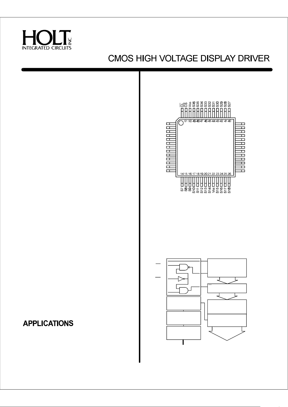
DichroicLiquidCrystalDisplays
StandardLiquidCrystalDisplays
VacuumFluorescentDisplays
!
!
!
!
!
!
!
!
!
5voltinputtranslatedto30voltsorless
Pin-outadaptabletodrive30,32or38
LCDsegments
RCoscillatororhighvoltage(BP)clockinput
TTLcompatibleinputs(HI-8010only)
CMOScompatibleinputs(HI-8110only)
Lowpowerconsumption
Industrial(-40°Cto+85°C)&Military(-55°C
to+125°C)temperatureranges
PinforpincompatiblewiththeMicrel
MIC8010/8011seriesandtheAMIS4520
seriesdrivers
Cascadable
Militarylevelprocessingavailable
!
PINCONFIGURATION (TopView)
FUNCTIONALBLOCKDIAGRAM
Þ BP
Oscillator
Divider
Voltage
Translator
HighVoltage
Buffer
38Stage
ShiftRegister
38BitLatch
Voltage
Translators
HighVoltage
Drivers
SEGMENTS
DATAIN
CLK
LE
Þ
Þ
Þ
DOUT38
DOUT32
DOUT30
GENERALDESCRIPTION
DIN Þ
CL Þ
CS Þ
LD Þ
LCDØ Þ
LCDØOPT Þ
(Seepage3-6foradditionalpackagepinconfigurations)
FEATURES
January2001
39
38
37
36
35
34
33
32
31
30
29
28
S26
S25
S24
S23
S22
S21
S20
DOUT38
N/C
N/C
N/C
BP
S19
2
3
4
5
6
7
8
9
10
11
12
LD
DIN
LCDØ
LCDØOPT
V
S37
S38
S1
S2
S3
S4
S5
S6
DD
HI-8010PQI
HI-8110PQI
HI-8010PQT
&
HI-8110PQT
52-PIN
PLASTICPQF
HOLTINTEGRATEDCIRCUITS
3-3(DS8010,Rev.C)01/01

FUNCTIONALDESCRIPTION
WheneveraLogic"0"isappliedtotheChipSelect()
input,onebitofdataisclockedintotheshiftregisterfromthe
serialdatainput(DIN)witheachnegativetransitionofthe
Clock()input.isinternallytiedtoVSSonsome
versions.ALogic"1"presentattheLoad(LD)inputwill
causeaparalleltransferofdatafromtheshiftregistertothe
datalatch.IftheLoad(LD)inputisheldhighwhiledatais
clockedintotheshiftregister,thelatchwillbetransparent.
Todisplaysegments,aLogic"1"isstoredintheappropriate
shiftregisterbitposition,andthesegmentoutputisout-ofphase withthebackplane.
Thebackplaneoutputfunctionsin1of2modes;externally
drivenorself-oscillating.WhentheLCDØinputisexternally
drivenwiththeLCDØOPTinputopencircuit(Figure2),the
backplaneoutputwillbein-phasewithLCDØ.Utilizingthe
self-oscillatingmode,inputsLCDØandLCDØOPTaretied
togetherandconnectedtoanRCcircuit(Figure3).
A150Kresistorwitha470pFcapacitorgeneratesan
approximatebackplanefrequencyof100Hz.The
LCDØ/LCDØOPToscillatorfrequencyisdividedby256to
determinethebackplaneoutputfrequency.Theresistor
value(R)mustb eatleast30Kforproperself-oscillator
operation.
Fordisplayshavinganumberofsegmentsgreaterthan38,
twoormoreofthedisplaydriversmaybecascadedtogether
byconnectingtheserialdataoutput(DOUT)fromthefirst
driver,totheserialdatainput(DIN)ofthefollowingdriver,
etc.(SeeFigures2&3).Dataout(DOUT)willchangestate
CS
CLCS
W
AllfourlogicinputsareTTLcompatibleontheHI-8010and
CMOScompatibleontheHI-8110.
W
HI-8010/HI-8110Series
TIMINGDIAGRAM
t
CSH
t
CSS
t
DS
t
DH
t
CL
t
CDO
t
LS
t
LW
t
CSL
t
LCS
CL
INPUT
DIN
INPUT
CS
INPUT
LD
INPUT
DOUT
OUTPUT
VALID
VALID
INTERNALOSCILLATORCIRCUIT
TOBACKPLANE
TRANSLATOR
ANDDRIVER
÷256
LCDØ
OPT
LCDØ
Figure1
Q
ontherisingedgeoftheClock().Clock(),Load(LD)
andChipSelect()shouldbetiedincommonwitheach
other,respectively,betweenallcascadeddisplaydrivers.
CLCL
CS
HOLTINTEGRATEDCIRCUITS
3-4
HI-8010/HI-8110Series
DCELECTRICALCHARACTERISTICS
VDD=5V,VEE=-25V,VSS=0V,TA=OperatingTemperatureRange(unlessotherwisespecified).
PARAMETERSYMBOLCONDITIONMINTYPMAXUNITS
OperatingVoltageVDD3.07.0V
SupplyCurrentIDDStatic,NoLoad200µA
IEEStatic,NoLoadf=100Hz150µA
InputLowVoltage,HI-8010(exceptLCDØ)VIL00.8V
InputHighVoltage,HI-8010(exceptLCDØ)VIH2VDDV
InputLowVoltage,HI-8110(exceptLCD)VIL00.3VDDV
InputHighVoltage,HI-8110(exceptLCD
InputLowVoltage(LCDØ)VILXVEE3V
InputHighVoltage(LCDØ)VIHX3.5VDDV
InputCurrentIINVIN=0to5V1µA
InputCapacitance(nottested)CI5pF
SegmentOutputImpedanceRSEGIL=10µA10,000
BackplaneOutputImpedanceRBPIL=10µA450
DataOutCurrent:IDOHSourceCurrent,VOH=4.5V-0.6mA
I DOLSinkCurrent,VOL=0.5V0.6mA
BP
TTL
TTL
CMOS
W
W
Ø
Ø)VIH0.7VDDVDDVCMOS
PARAMETERSYMBOLVDDMINTYPMAXUNITS
CLClockPeriodt5V1200ns
ClockPulseWidtht5V520ns
DataIn-Setupt5V50ns
DataIn-Holdt5V400ns
ChipSelect-SetuptoClockt5V200ns
ChipSelect-HoldtoClockt5V450ns
Load-SetuptoClockt5V500ns
ChipSelect-SetuptoLoadt5V300ns
LoadPulseWidtht5V500ns
ChipSelect-HoldtoLoadt5V300ns
CW
DS
DH
CSS
CSH
LS
CSL
LW
LCS
DataOutValid,fromClockt5V800nsCDO
ACELECTRICALCHARACTERISTICS
VDD=5V,VEE=-25V,VSS=0V,TA=OperatingTemperatureRange(unlessotherwisespecified).
ABSOLUTEMAXIMUMRATINGS
NOTE:Stressesabovethoselistedunder"AbsoluteMaximumRatings"maycausepermanentdamagetothedevice.Thesea restressratingsonly.
Functionaloperationofthedeviceattheseoranyotherconditionsabovethoseindicatedintheoperationalsection softhespecificationsisnotimplied.
Exposuretoabsolutemaximumratingconditionsforextendedperiodsmayaffectdevicereliability.
VoltagesreferencedtoVSS=0V
VDD........................
VEE................
SupplyVoltage
VDD-35Vto0V
0Vto7V
Voltageatanyinput,exceptLCD..-0.3toVDD+0.3VØ
Voltageatinput...............VDD-35toVDD+0.3VLCDØ
DCCurrentanyinputpin...................................10mA
PowerDissipation......................................................300mW
OperatingTemperatureRange-Hi-Temp/Mil..-55°to+125°C
StorageTemperatureRange...........................-65°to+150°C
OperatingTemperatureRange-Industrial........-40°to+85°C
HOLTINTEGRATEDCIRCUITS
3-5
 Loading...