

HOLT HI-8040QT, HI-8040QM-01, HI-8040Q Datasheet
September1999
HI-8040
GENERALDESCRIPTION
TheHI-8040isaCMOSintegratedcircuitdesignedforhigh
voltageLCDdisplaydriveapplications.Itcandrive85
segmentsatvoltagesbetween+5and-30volts.Anoptional
negativeconvertercangeneratethenegativedisplaydrive
voltage.Testinputsfacilitateopensandshortstesting.The
backplanefrequencyischeckedand,aslongaspoweris
available,thesegmentsareshut"Off"ifthefrequency
becomestoolow.
TheHI-8040ispartofafamilyofdisplaydriverswhich
controlsegmentinformationinthesameway.Datais
seriallyclockedintothedeviceandthedataforallsegment
out putsarelatchedinparallelwhentheLoadinput
transitionsfromhightolow.WiththeDataOutfromtheshift
registeravailable,devicesmaybecascadedtoobtainmore
segmentoutputs.Theshiftregisteris85bitslong.
Thedieismetalmaskprogrammabletoprovideforvarious
packageand/orcascadetapoptions.ConsultyourHolt
Salesrepresentativetoexplorethepossibilities.
APPLICATIONS
!
DichroicLiquidCrystalDisplays
!
StandardLiquidCrystalDisplays
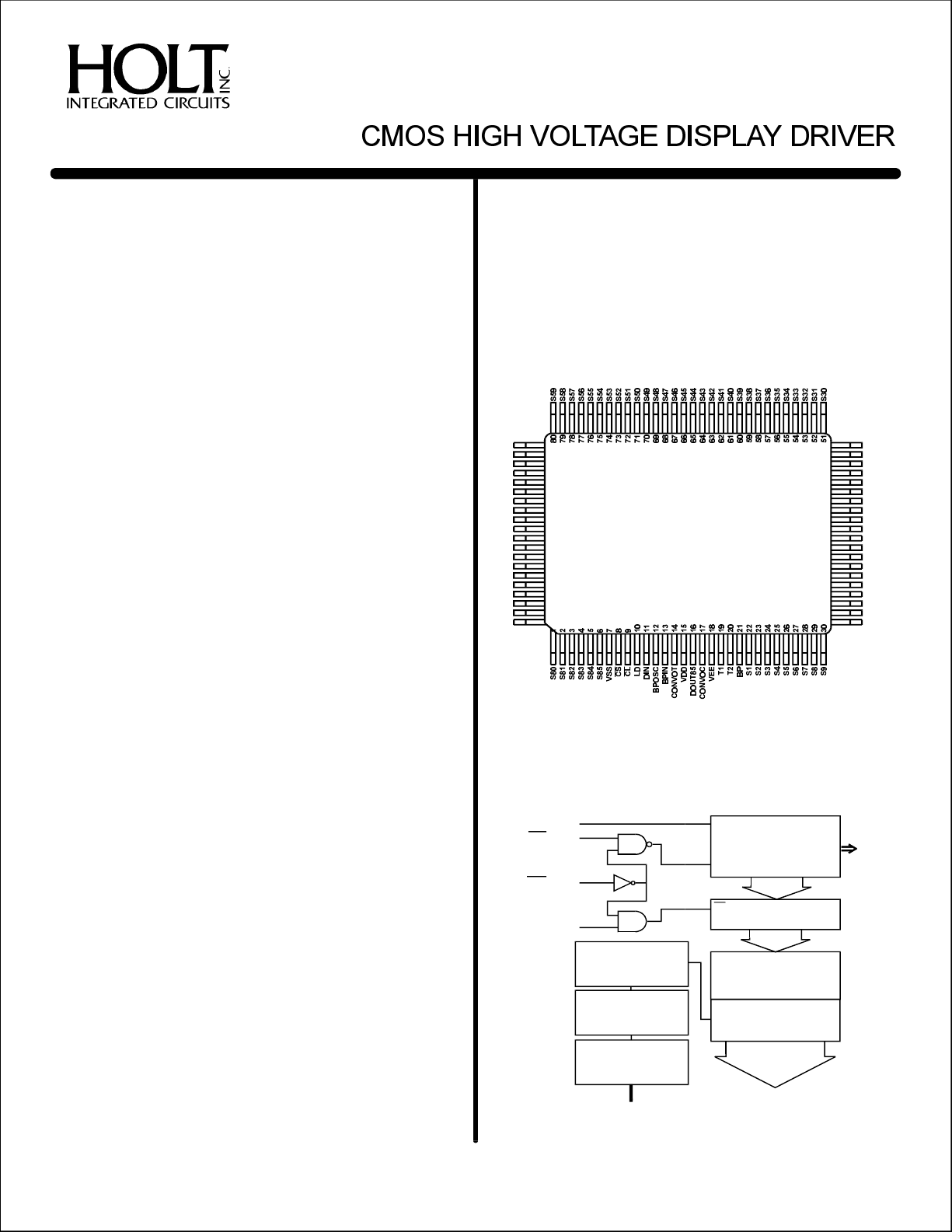
PINCONFIGURATION (TopView)
S60
S61
S62
S63
S64
S65
S66
S67
S68
S69
S70
S71
S72
S73
S74
S75
S76
S77
S78
S79
81
82
83
84
85
86
87
88
89
90
91
92
93
94
95
96
97
98
99
100
100PINQUADCERPACK
50
49
48
47
46
45
44
43
42
41
40
39
38
37
36
35
34
33
32
31
S29
S28
S27
S26
S25
S24
S23
S22
S21
S20
S19
S18
S17
S16
S15
S14
S13
S12
S11
S10
FEATURES
!
4MHzserialinputdatarate
!
85segmentoutputs
!
Cascadable
!
5Voltinputstranslatedto35Volts
!
estpinsallowhardwareall"ON",all"OFF"or
T
alternating
!
Monitorsbackplaneoscillationandforcesall
segmentsto"OFF"conditionifbelow10Hz
!
Negativevoltageconverteravailableon-chip
!
CMOSlowpower
!
Militaryprocessingavailable
Seepage3-19formagnifiedview
FUNCTIONALBLOCKDIAGRAM
DIN
BPOSC
BPIN
Þ
Þ
CL
Þ
CS
LD
Þ
Oscillator
Þ
Þ
Divider
Voltage
Translator
HighVoltage
Buffer
Þ BP
DATAIN
85Stage
ShiftRegister
CLK
LE
85BitLatch
Voltage
Translators
HighVoltage
Drivers
85SEGMENTS
DOUT
85
HOLTINTEGRATEDCIRCUITS
3-15(DS8040Rev.NEW)9/99
FUNCTIONALDESCRIPTION
HI-8040
INPUTLOGIC
mustbeheldlowtoenterdataintotheshiftregister.
CS
Thedataisclockedonthenegativeedgeof.LDisnor-
CL
mallyheldlowandonlypulsedhighwhennewdataisready
fordisplay.WhenLDishighthelatchistransparent.Allfour
logicinputsareTTLcompatible.Alogic"1"atDINthatis
eventuallylatchedtothesegmentdriverswillcausethesegmenttobeattheoppositevoltageleveloftheBPpin(outof
phase).
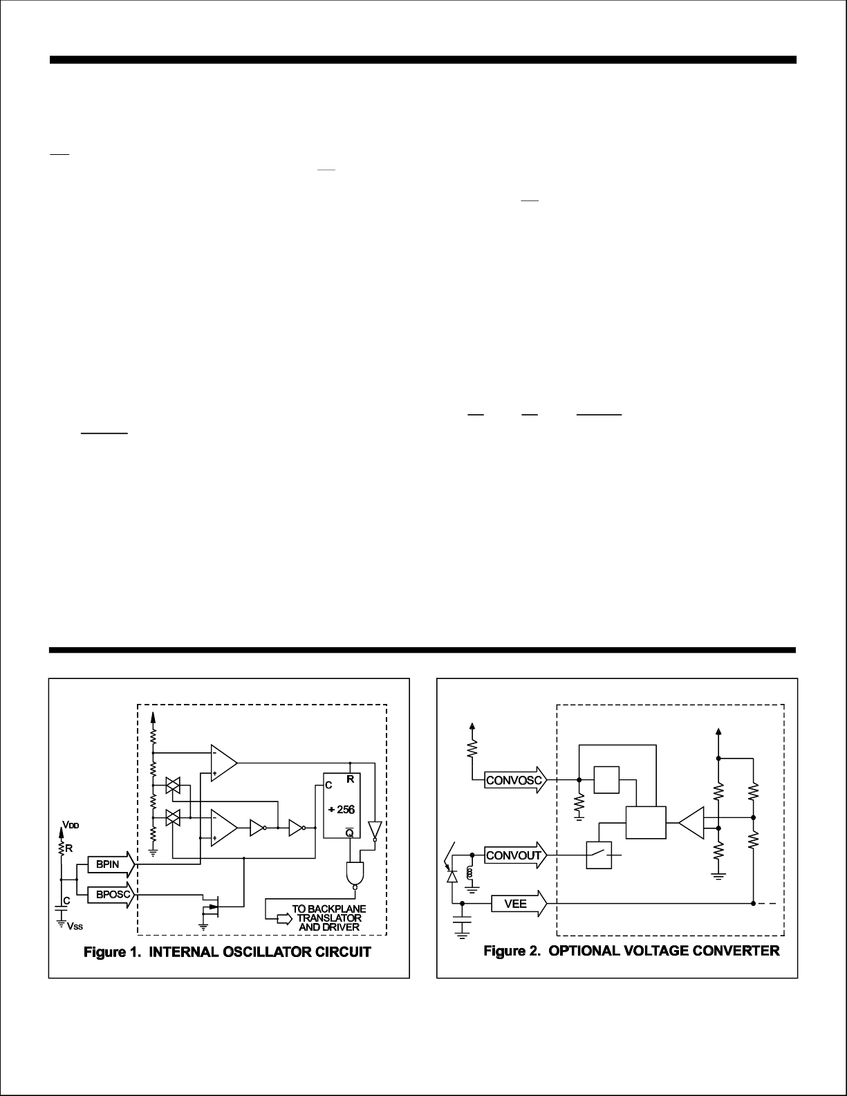
BPOSCandBPIN
Theusercaneithermakeanoscillatortocreatethe
backplanefrequencyordriveasignalintoBPINleaving
BPOSCopen.Tomakeanoscillator,pinsBPOSCand
BPINmustbeconnectedtogeth erandtheappropriateR
andCcombinationapplied(SeeFigure1).Iftheoscillatoris
used,thebackplanefrequencyisapproximately
f=.(forR=180KC=220pF,f100Hz).
BPBP
1
256RC
W&»
VEE&NEGATIVEVOLTAGECONVERTER
VEEmaybeexternallydriventoamaximum-30V.Alternatively,thereisavoltageconverterthatwillprovide-21.4volts
(SeeFigure2).Iftheconverterpinsareleftopencircuit,an
on-chipsenseresistorwillcauseshutdownofallcurrent
consumptionassociatedwiththeconverter.Theconverter
willsurviveashortedsegmentconditionandcontinueto
maintainVEEat-20volts.
DOUT
TheDOUTpinisavailablefromsegment85forcascading
devicestodrivemoresegmentsandforverifyingthedata
integrity.Thisoutputcandrive2TTLloads.Itchangesonthe
positiveedgeof.
CL
AUTOMATICSEGMENTSOFF
Theinternalbackplanesignalistestedcontinuouslytobeat
least10Hz.Ifthedetectorsensesf<10Hz,thenthesegments
areforcedtothesamevoltageasthebackplane(allsegments
in"OFF"state).However,thedetectorisonlyfunctionalwhile
VDDisabovetheminimumoperatingvoltagespecification.
TESTINPUTS
Thetestfunctionsavailableare:
T2T1Display
00Normal
01AllOff
10AllOn
11AlternatingOn/OffSegments
Th etestinputsmustbetiedtotheappropriatelogiclevelfor
correctcircuitoperation.
V DD
R330K W
IN5818,IN5819
330µh
V SS
10µF
V SS
HOLTINTEGRATEDCIRCUITS
3-16
R
OSC
SENSE
Control
V DD
 Loading...