

HOLT HI-3282PQT, HI-3282PQI, HI-3282PJT, HI-3282PJI, HI-3282CDT Datasheet
...
HI-3282
GENERALDESCRIPTION
TheHI-3282isasilicongateCMOSdeviceforinterfacing
theARINC429serialdatabustoa16-bitparalleldatabus.
Tworeceiversandanindependenttransmitterare
provided.Thereceiverinputcircuitryandlogicare
designedtomeettheARINC429specificationsforloading,
leveldetection,timing,andprotocol.Thetransmitter
sectionprovidestheARINC429communicationprotocol.
AdditionalinterfacecircuitrysuchastheHoltHI-8382orHI8585arerequiredtotranslatethe5voltlogicoutputsto
ARINC429drivelevels.
The16-bitparalleldatabusexchangesthe32-bitARINC
da tawordintwostepswheneitherloadingthetransmitter
orinterrogatingthereceivers.Thedatabusinterfaceswith
CMOSandTTL.
Timingofallthecircuitrybeginswiththemasterclockinput,
CLK.ForARINC429applications,themasterclock
frequencyis1MHz.
Eachindependentreceivermonitorsthedatastreamwitha
samplingrate10timesthedatarate.Thesamplingrateis
softwareselectableateither1MHzor125KHz.Theresults
ofaparitycheckareavailableasthe32ndARINCbit.
FEATURES
!
ARINCspecification429compatible
!
CompatiblewithIndustry-standardalternate
Parts
!
Smallfootprint44PQFPpackageoption
!
16-Bitparalleldatabus
!
DirectreceiverinterfacetoARINCbus
!
Timingcontrol10timesthedatarate
!
Selectabledataclocks
!
Automatictransmitterdatatiming
!
Selftestmode
!
Parityfunctions
!
Lowpower,single5voltsupply
!
Industrial&fullmilitarytemperatureranges
ThetransmitterhasaFirstIn,FirstOut(FIFO)memoryto
store8ARINCwordsfortransmission.Thedatara teofthe
transmitterissoftwareselectablebydividingthemaster
clock,CLK,byeither10or80.Themasterclockisusedto
setthetimingoftheARINCtransmissionwithintherequired
resolution.
APPLICATIONS
!
Avionicsdatacommunication
!
Serialtoparallelconversion
!
Paralleltoserialconversion
N/C-1
D/R1
D/R2
SEL-4
EN1
EN2
BD15-7
BD14-8
BD13-9
BD12-10
BD11-11
33-N/C
-2
-3
-5
-6
HI-3282PQI
&
HI-3282PQT
32-N/C
31-X
CWSTR
30-ENTX
29-
429DO
28-429DO
27-TX/R
26-
PL2
25-
PL1
24-BD00
23-BD01
HOLTINTEGRATEDCIRCUITS
1(DS3282Rev.E)05/01

PINDESCRIPTION
SYMBOLFUNCTIONDESCRIPTION
VCCPOWER+5V±5%
429DI1(A)INPUTARINCreceiver1positiveinput
429DI1(B)INPUTARINCreceiver1negativeinput
429DI2(A)INPUTARINCreceiver2positiveinput
429DI2(B)INPUTARINCreceiver2negativeinput
D/R1
D/R2
SELINPUTReceiverdatabyteselection(0=BYTE1)(1=BYTE2)
EN1
EN2EN1
BD15I/ODataBus
BD14I/ODataBus
BD13I/ODataBus
BD12I/ODataBus
BD11I/ODataBus
BD10I/ODataBus
BD09I/ODataBus
BD08I/OData Bus
BD07I/ODataBus
BD06I/ODataBus
GNDPOWER0V
BD05I/ODataBus
BD04I/ODataBus
BD03I/ODataBus
BD02I/ODataBus
BD01I/ODataBus
BD00I/ODataBus
PL1
PL2PL1.
TX/ROUTPUTTransmitterreadyflag.GoeslowwhenARINCwordloadedintoFIFO.Goeshigh
429DOOUTPUT"ONES"dataoutputfromtransmitter.
429DO
ENTXINPUTEnableTransmission
CWSTR
CLKINPUTMasterClockinput
TXCLKOUTPUTTransmitterClockequaltoMasterClock(CLK),dividedbyeither10or80.
MR
DBCEN
OUTPUTReceiver1datareadyflag
OUTPUTReceiver2datareadyflag
INPUTDataBuscontrol,enablesreceiver1datatooutputs
INPUTDataBuscontrol,enablesreceiver2datatooutputsifishigh
INPUTLatchenableforbyte1enteredfromdatabustotransmitterFIFO.
INPUTLatchenableforbyte2enteredfromdatabustotransmitterFIFO.Mustfollow
OUTPUT"ZEROES"dataoutputfromtransmitter.
INPUTClockforcontrolwordregiste r
INPUTMasterReset,activelow
INPUTDatabitcontrolEnable.(Activelow,withinternalpulluptoVDD).
HI-3282
aftertransmissionandFIFOempty.
HOLTINTEGRATEDCIRCUITS
2
HI-3282
FUNCTIONALDESCRIPTION
CONTROLWORDREGISTER
TheHI-3282contains11dataflipflopswhoseDinputsareconnectedtothedatabusandclocksconnectedto.Each
flipflopprovidesoptionstotheuserasfollows:
DATA
BUSFUNCTIONCONTROLDESCRIPTION
PIN
BD04PARENEnablesparitybitinsertioninto
Transmitterdatabit32
Ifenabled,aninternalconnection
BDO5SELFTEST0=ENABLEismadepassing429DOand
429DO
RECEIVER1Ifenabled,ARINCbits9and,
BDO6DECODER1=ENABLE10mustmatchthenexttwo
IfReceiver1Decoderis
BDO7--enabled,theARINCbit9
IfReceiver1Decoderis
BDO8--enabled,theARINCbit10
RECEIVER2Ifenabled,ARINCbits9and
BDO9DECODER1=ENABLE10mustmatchthenexttwo
IfReceiver2Decoderis
BD10--enabled,thenARINCbit9
CWSTR
tothereceiverlogicinputs
controlwordbits
mustmatchthisbit
mustmatchthisbit
controlwordbits
mustmatchthisbit
ARINC429DATAFORMAT
Thefollowingtableshowsthebitpositionsinexchangingdatawith
thereceiverorthetransmitter.ARINCbit1isthefirstbit
transmittedorreceived.
BYTE1
DATABDBDBDBDBDBDBDBDBDBDBDBDBDBDBDBD
BUS15141312111009080706050403020100
ARINC13121110931303212345678
BIT
BYTE2
DATABDBDBDBDBDBDBDBDBDBDBDBDBDBDBDBD
BUS15141312111009080706050403020100
ARINC29282726252423222120191817161514
BIT
THERECEIVERS
ARINCBUSINTERFACE
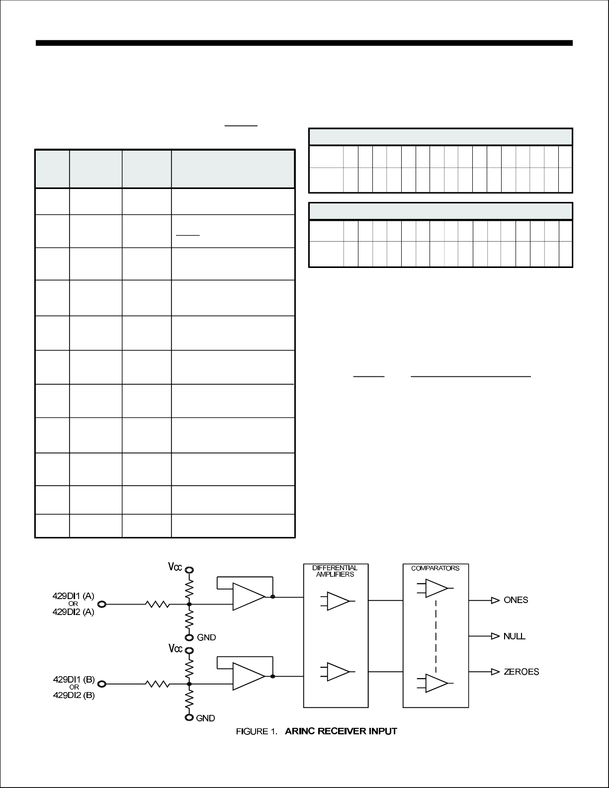
Figure1showstheinputcircuitforeachreceiver.TheARINC429
specificationrequiresthefollowingdetectionlevels:
STATEDIFFERENTIALVOLTAGE
ONE+6.5Voltsto+13Volts
NULL+2.5Voltsto-2.5Volts
ZERO-6.5Voltsto-13Volts
BD11--enabled,thenARINCbit10
IfReceiver2Decoderis
mustmatchthisbit
INVERTLogic0enablesnormaloddparity
BD12XMTR1=ENABLEandLogic1enablesevenparity
PARITYoutputintransmitter32ndbit
BD13XMTRDATA0=÷10CLKisdividedeitherby10or
CLKSELECT1=÷8080toobtainXMTRdataclock
BD14RCVRDTA0=÷10CLKisdividedeitherby10or
CLKSELECT1=÷8080toobtainRCVRdataclock
TheHI-8382guaranteesrecognitionoftheselevelswithacommon
modeVoltagewithrespecttoGNDlessthan±5Vfortheworstcase
condition(4.75Vsupplyand13Vsignallevel).
Thetolerancesinthedesignguaranteedetectionoftheabove
levels,sotheactualacceptancerangesareslightlylarger.Ifthe
ARINCsignalisoutoftheactualacceptanceranges,includingthe
nulls,thechiprejectsthedata.
HOLTINTEGRATEDCIRCUITS
3
HI-3282
FUNCTIONALDESCRIPTION(con't)
RECEIVERLOGICOPERATION
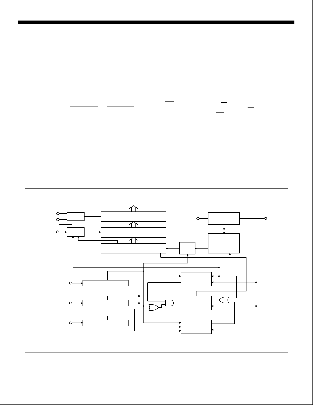
Figure2showsablockdiagramofthelogicsectionofeachreceiver.
BITTIMING
TheARINC429specificationcontainsthefollowingtiming
specificationforthereceiveddata:
HIGHSPEEDLOWSPEED
BITRATE
PULSERISETIME
PULSEFALLTIME
PULSEWIDTH
100KBPS±1%12K-14.5KBPS
1.5±0.5µsec10±5µsec
1.5±0.5µsec10±5µsec
5µsec±5%34.5to41.7µsec
RECEIVERPARITY
ThereceiverparitycircuitcountsOnesreceived,includingthe
paritybit,ARINCbit32.Iftheresultisodd,then"0"willappearin
the32ndbit.
TOPINS
RETRIEVINGDATA
Once32validbitsarerecognized,thereceiverlogicgenerates
anEndofSequence(EOS).Ifthereceiverdecoderisenabled
andthe9thand10thARINCbitsmatchthecontrolword
programbitsorifthereceiverdecoderisdisabled,thenEOS
clocksthedatareadyflagflipfloptoa"1",or(orboth)
D/R1D/R2
willgolow.Thedataflagforareceiverwillremainlowuntilafter
ARINCbytesfromthatreceiverareretrieved.Thisis
both
accomplishedbyactivatingwithSEL,thebyteselector,low
toretrievethefirstbyteandactivatingwithSELhighto
retrievethesecondbyte.retrievesdatafromreceiver1and
ret rievesdatafromreceiver2.
EN2
EN
EN
ENI
IfanotherARINCwordisreceived,andanewEOSoccurs
beforethetwobytesareretrieved,thedataisoverwrittenbythe
newword.
DECODER
CONTROL
BITS
SEL
EN
D/R
ZEROS
ONES
NULL
MUX
CONTROL
LATCH
ENABLE
/
CONTROL
BITS9&10
EOS
SHIFTREGISTER
SHIFTREGISTER
SHIFTREGISTER
32TO16DRIVER
32BITLATCH
32BITSHIFTREGISTER
DATA
BITCLOCK
WORDGAP
START
CONTROL
BITBD14
PARITY
CHECK
WORDGAP
SEQUENCE
CONTROL
DETECTION
TIMER
ERROR
32ND
CLOCK
OPTION
CLOCK
BIT
COUNTER
AND
BIT
SEQUENCE
EOS
BITCLOCK
END
ERROR
CLOCK
ENDOF
CLK
FIGURE2. RECEIVERBLOCKDIAGRAM
HOLTINTEGRATEDCIRCUITS
4
 Loading...