

HOLT HI-3188PST, HI-3188PSI, HI-3187PST, HI-3187PSI, HI-3186PST Datasheet
...
HI-3182,HI-3183,HI-3184,HI-3185
HI-3186,HI-3187,HI-3188
March2001
TheHI-3182,HI-3183,HI-3184,HI-3185,HI-3186,HI-3187and
HI-3188businterfaceproductsaresilicongateCMOSdevices
designedasalinedriverinaccordancewiththeARINC429bus
specifications.InadditiontobeingfunctionalupgradesofHolt's
HI-8382&HI-8383products,theyarealsoalternatesourcesfor
theHS-3182(Intersil/Harris),theRM3182(Fairchild/Raytheon)
andavarietyofsimilarDEI/DDClinedriverproducts.
Inputsareprovidedforclockingandsynchronization.These
signalsareAND'dwiththeDATAinputstoenhancesystem
performanceandallowtheHI-318Xs eriesofproductstobe
usedinavarietyofapplications.Bothlogicandsynchronization
inputsfeaturebuilt-in2,000VminimumESDinputprotectionas
wellasTTLandCMOScompatibility.
ThedifferentialoutputsoftheHI-318Xseriesofproductsare
independentlyprogrammabletoeitherthehighspeedorlow
speedARINC429outputriseandfalltimespecificationsthrough
theuseoftwoexternalcapacitors.Theoutputvoltageswingis
alsoadjustablebytheapplicationofanexternalvoltagetothe
VREFinput.Productswith0,13or37.5ohmresistorsinseries
witheachARINCoutputareav ailable.Inaddition,the
HI-3184andHI-3187productsalsohavea
eachoutput.
fuseinserieswith
HI-3182,
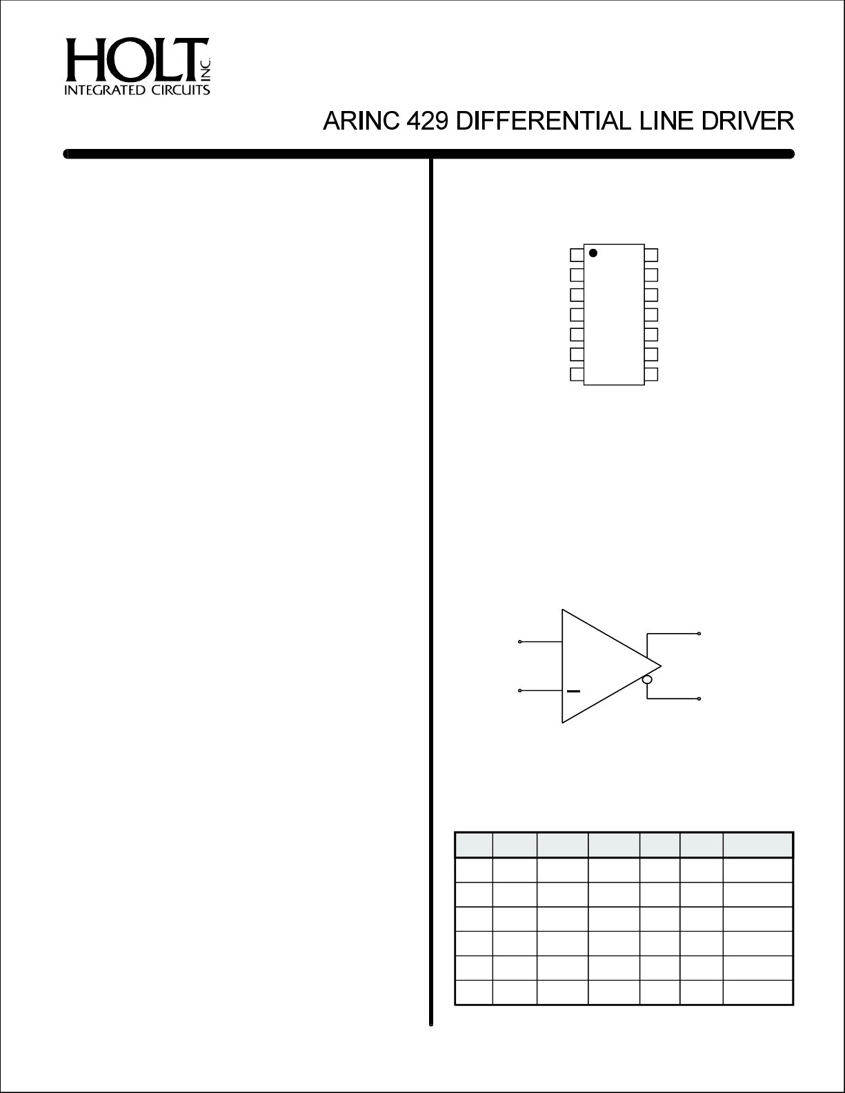
PINCONFIGURATION (TopView)GENERALDESCRIPTION
14V
V1
REF
GND(SeeNote*)2
SYNC3
DATA(A)4
C5
A
A6
OUT
-V7
1
13CLOCK
12DATA(B)
11C
B
10B
OUT
9+V
8GND
HI-3184PS,HI-3185PS,HI-3186PS
&HI-3187PS
14-PINPLASTICSMALLOUTLINE(ESOIC) **
Notes:*Pin2maybeleftfloating
**ThermallyEnhancedSOICPackage
(SeePage5foradditionalpackagepinconfigurations)
FUNCTION
TheHI-318Xseriesoflinedriversareintendedforusewhere
logicsignalsmustbeconvertedtoARINC429levelssuchas
whenusinganASIC,theHI-8282ARINC429SerialTransmitter/DualReceiver,theHI-6010ARINC429Transmitter/Receiver
ortheHI-8783ARINCInterfaceDevice.Holtproductsare
readilyavailableforbothindustrialandmilitaryapplications.
PleasecontacttheHoltSalesDepartmentforadditional
information.
FEATURES
!
LowpowerCMOS
!
TTLandCMOScompatibleinputs
!
Programmableoutputvoltageswing
!
AdjustableARINCriseandfalltimes
Plastic14&16-pinthermallyenhancedSOIC
!
packagesavailable
Pin-for-PinalternativeforDEI/DDC/Intersil/Fairchild
!
applications
!
Operatesatdataratesupto100Kbits
!
Overvoltageprotection
!
IndustrialandMilitarytemperatureranges
+
ARINC429DIFFERENTIALLINEDRIVER
TRUTHTABLE
SYNCCLOCKDATA(A)DATA(B)AOUTBOUTCOMMENTS
XLXX0V0VNULL
LXXX0V0VNULL
HHLL0V0VNULL
HHLH-V+VLOW
HHHL+V-VHIGH
HHHH0V0VNULL
REFREF
REFREF
HOLTINTEGRATEDCIRCUITS
(DS3182Rev.B)03/01
1
HI-3182,HI-3183,HI-3184,HI-3185,HI-3186,HI-3187,HI-3188
FUNCTIONALDESCRIPTION
TheSYNCandCLOCKinputsestablishdatasynchronization
utilizingtwoANDgates,oneforeachdatainput.Eachlogic
input,includingthepowerenable()input,are
STROBE
TTL/CMOScompatible.
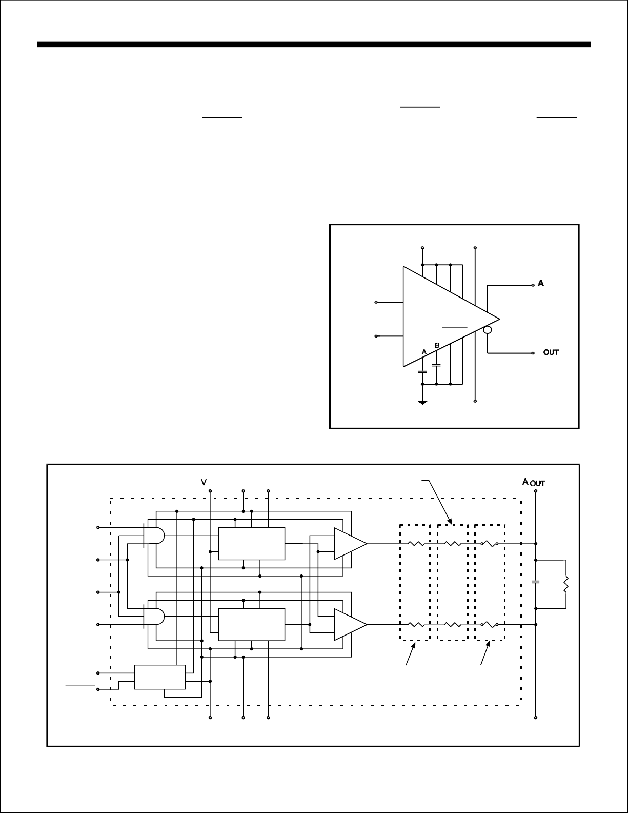
Figure1illustratesatypicalARINC429busapplication.
ThreepowersuppliesarenecessarytooperatetheHI-3182;
typically+15V,-15Vand+5V.Thechipalsoworkswith±12V
supplies.The+5Vsupplycanalsoprovideareference
voltagethatdeterminestheoutputvoltageswing.The
differentialoutputvoltageswingwillequal2V.Ifavalueof
Votherthan+5Visneeded,aseparate+5Vpowersupply
REF
isrequ iredforpinV.
1
REF
WiththeDATA(A)inputatalogichighandDATA(B)inputata
logiclow,Awillswitchtothe+VrailandBwill
switchtothe-Vrail(ARINCHIGHstate).Withbothdata
OUTREFOUT
REF
inputsignalsatalogiclowstate,theoutputswillbothswitchto
0V(ARINCNULLstate).
Thedriveroutputimpedance,R,isnominally75,26or0
OUT
ohmsdependingontheoptionchosen.Theriseandfalltimes
oftheoutputscanbecalibratedthroughtheselectionoftwo
externalcapacitorvaluesthreconnectedtotheCandC
ata
AB
inputpins.Typicalvaluesforhigh-speedoperation
(100KBPS)areC=C=75pFandforlow-speedoperati on
(12.5to14KBPS)C=C=500pF.
AB
AB
TheARINCoutputscanbeputinatri-statemodebyapplying
alogichightotheinputpin.Ifthisfeatureisnot
beingused,thepinshouldbetiedtoground.The
STROBE
STROBE
functionisnotavailableinthe14&16-pinSOICpackage
configurationswherethepinisinternallyconnectedto
ground.
TheARINCoutputsoftheHI-3182,HI-3184andHI-3187are
protectedbyinternalfusescapableofsinkingbetween800900mAforshortperiodsoftime(125s).
V
REF
V
1
DATA(A)
INPUTS TOARINCBUS
DATA(B)
SYNC
GND
C
C
CLOCK
STROBE
µ
+15V+5V
OUT
+V
-V
B
TheCandCpinsswingbetween+5Vandgroundallowing
AB
theswitchingofcapacitorvalueswithanexternalsinglesupplyanalogswitch.
+V
C
A
DATA(A)
CLOCK
SYNC
DATA(B)
STROBE
REF
LEVELSHIFTER
ANDSLOPE
CONTROL(A)
LEVELSHIFTER
ANDSLOPE
CONTROL(B)
V 1
CURRENT
REGULATOR
Figure1. ARINC429BUSAPPLICATION
Shortedon
HI-3186,HI-3187,HI-3188
OUTPUT
DRIVER(A)
OUTPUT
DRIVER(B)
Shortedon
HI-3183,HI-3186
HI-3187,HI-3188
24.5 Ω
24.5Ω
-15V
13 Ω
13 Ω
F A
F B
Shortedon
HI-3183,HI-3185
HI-3186,HI-3188
C L
R L
-V
CGND
B
Figure2. FUNCTIONALBLOCKDIAGRAM
HOLTINTEGRATEDCIRCUITS
2
B
OUT
HI-3182,HI-3183,HI-3184,HI-3185,HI-3186,HI-3187,HI-3188
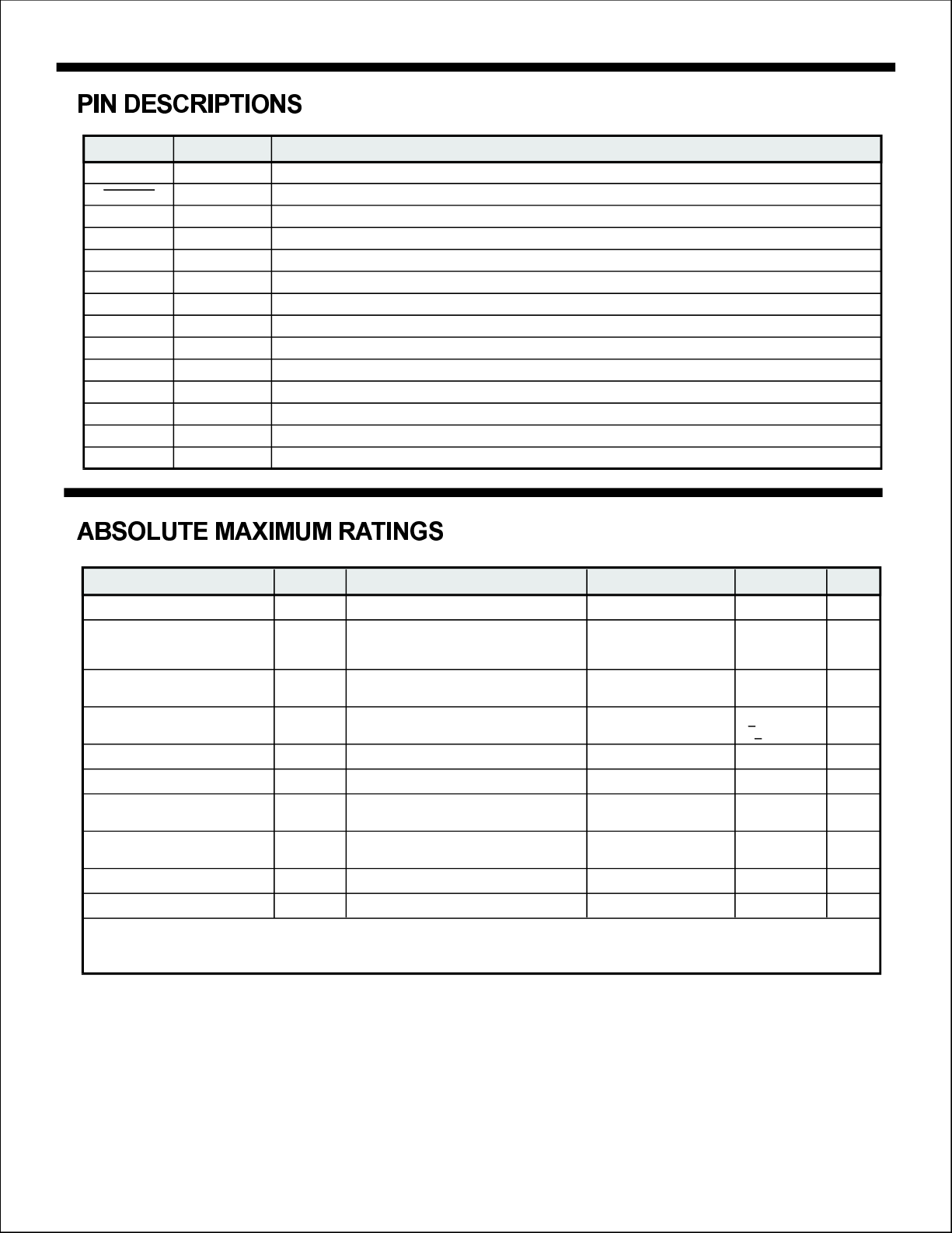
SYMBOLFUNCTIONDESCRIPTION
VPOWERReferencevoltageusedtodeterminetheoutputvoltageswing
REF
STROBE
SYNCINPUTSynchronizesdatainputs
DATA(A)INPUTDatainputterminalA
CINPUTConnectionforDATA(A)slew-ratecapacitor
A
AOUTPUTARINCoutputterminalA
OUT
-VPOWER-12Vto-15V
GNDPOWER0.0V
+VPOWER+12Vto+15V
BOUTPUTB
OUT
CINPUT
B
DATA(B)INPUTB
CLOCKINPUTSynchronizesdatainputs
VPOWER+5V±5%
1
INPUTAlogichightri-statestheARINCoutputs.Notavailableinthe14-pinSOICpackage(tiedtoGNDinternally).
ARINCoutputterminal
ConnectionforDATA(B)slew-ratecapacitor
Datainputterminal
AllVoltagesreferencedtoGND,TA=OperatingTemperatureRange(unlessotherwisespecified)
PARAMETERSYMBOLCONDITIONSOPERATINGRANGEMAXIMUMUNIT
DifferentialVoltageVVoltagebetween+Vand-Vterminals40V
DIF
SupplyVoltage+V+10.8to+16.5V
-V-10.8to-16.5V
V+5±10%+7V
1
VoltageReferenceVForARINC429+5±5%6V
REF
ForApplicationsotherthanARINC0to66V
InputVoltageRangeVGND-0.3V
IN
>
V1+0.3V
<
OutputShort-CircuitDurationSeeNote:1
OutputOvervoltageProtectionSeeNote:2
OperatingTemperatureRangeTHi-temp&Military-55to+125°C
A
Industrial-40to+85°C
StorageTemperatureRangeTCeramic&Plastic-65to+150°C
STG
LeadTemperatureSoldering,10seconds+275°C
JunctionTemperatureT+175°C
J
Note1.Heatsinkingmayberequired forOutputShortCircuitat+125°Candfor100KBPSat+125°C.
Note2.ThefusesusedforOutputOvervoltageProtectionmaybeblownbythepresenceofavoltageateitheroutputthat isgreater
than±12.0VwithrespecttoGND.(HI-3182,3184&3187only)
NOTE:Stressesabovethoselistedunder"AbsoluteMaximumRatings"maycausepermanentdamagetothedevice.Thesea restressratings
only.Functionaloperationofthedeviceattheseoranyotherconditionsabovethoseindicatedintheoperationalse ctionsofthespecifications
isnotimplied.Exposuretoabsolutemaximumratingconditionsforextendedperiodsmayaffectdevicereliability.
HOLTINTEGRATEDCIRCUITS
3
 Loading...