

March2001
HI-1567,HI-1568
DESCRIPTION
TheHI-1567andHI-1568arelowpowerCMOSdual
transceiversdesignedtomeettherequirementsof
MIL-STD-1553/1760specifications.
Thetransmittersectionofeachchanneltakes
complimentaryCMOS/TTLdigitalinputdataandconverts
ittobi-phaseManchesterencoded1553signalssuitable
fordrivingthebusisolationtransformer.Separate
transmitterinhibitcontrolsignalsareprovidedforeach
transmitter.
Thereceiversectionoftheeachchannelconvertsthe1553
busbi-phasedatatocomplimentaryCMOS/TTLdata
suitableforinputtingtoaManchesterdecoder.Each
receiver hasaseparateenableinputwhichcanbeusedto
forcetheoutputofthereceivertoalogic0(HI-1567)or
logic1(HI-1568).
Tominimizethepackagesizeforthisfunction,the
transmitteroutputsareinternallyconnectedtothereceiver
inputs,sothatonlytwopinsarerequiredforconnectionto
eachcouplingtransformer.Fordesignsrequiring
independentaccesstotransmitterandreceiver1553
signals,pleasecontactyourHoltSalesrepresentative.
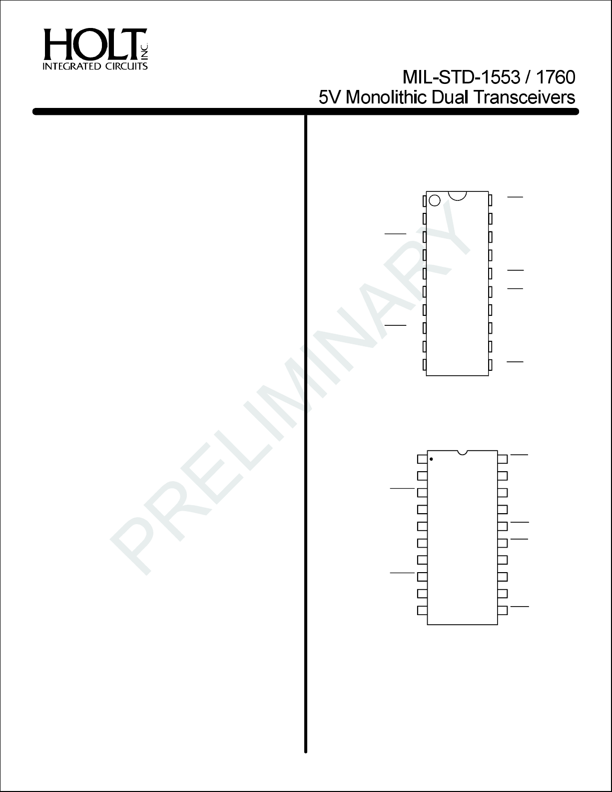
PINCONFIGURATIONS
VDDA1
BUSA2
3
BUSA
RXENA4
GNDA5
VDDB6
BUSB7
8
BUSB
RXENB9
GNDB10
20PinCeramicDIPpackage
20
TXA
19TXA
18TXINHA
17RXA
16
RXA
15
TXB
14TXB
13TXINHB
12RXB
11
RXB
FEATURES
!
ComplianttoMIL-STD-1553A&B,
MIL-STD-1760
!
CMOStechnologyforlowstandbypower
!
Smallestfootprintavailablein20pinplastic
ESOIC(thermallyenhancedSOIC)package
!
Lessthan1.0Wmaximumpowerdissipation
!
AvailableinDIP,Flatpackandsmalloutline
(ESOIC)packageoptions
!
Militaryprocessingoptions
!
Industrystandardpinconfigurations
VDDA
BUSA
BUSA
RXENA
GNDA
VDDB
BUSB
BUSB
RXENB
GNDB
1
2
3
4
5
6
7
8
9
10
20
19
18
17
16
15
14
13
12
11
TXA
TXA
TXINHA
RXA
RXA
TXB
TXB
TXINHB
RXB
RXB
20PinPlasticESOIC-WBpackage
HOLTINTEGRATEDCIRCUITS
(DS1567Rev.B)03/01
1
HI-1567,HI-1568
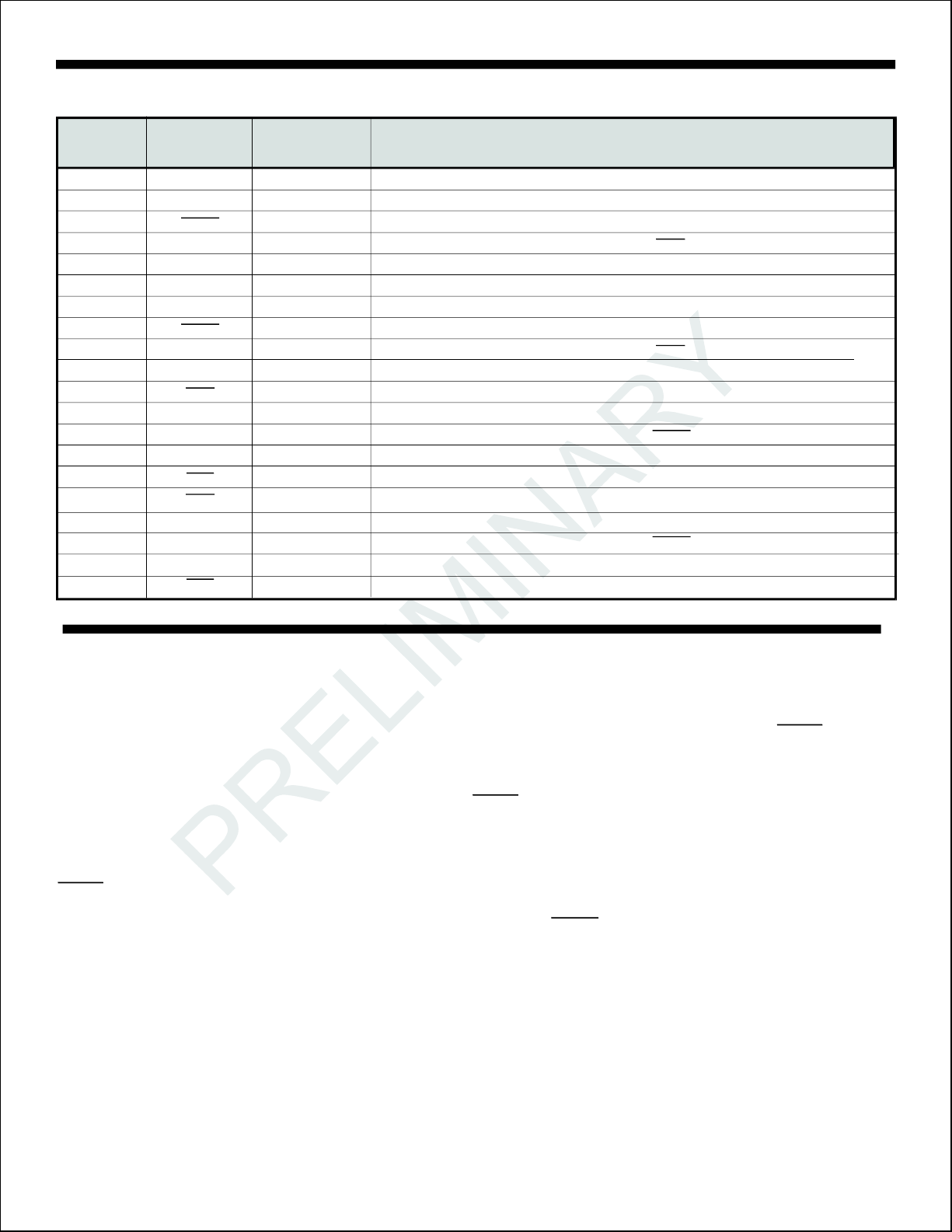
PINDESCRIPTIONS
PINSYMBOLFUNCTIONDESCRIPTION
1VDDApowersupply+5voltpowerforchannelA
2BUSAanalogoutputMIL-STD-1533busdriverA,positivesignal
3analogoutputMIL-STD-1553busdriverA,negativesignal
4RXENAdigitalinputReceiverAenable.Iflow,forcesRXAandlow(HI-1567)orHigh(HI-1568)
5GNDApowersupplyGroundforchannelA
6VDDB
7BUSB
8analogoutputMIL-STD-1553busdriverB,negativesignal
9RXENB
10GNDB
11
12RXBdigitaloutputReceiverBoutpot,non-invertedl
13TXINHBdigitalinputTransmitinhibit,channelB.IfhighBUSB,disabled
14TXBdigitalinputTransmitterBdigitaldatainput,non-inverted
15digitalinputTransmitterBdigitaldatainput,inverted
16 digitaloutput
17RXAdigitaloutputReceiverAoutput,non-inverted
18TXINHAdigitalinputTransmitinhibit,channelA.IfhighBUSA,disabled
19TXAdigitalinputTransmitterAdigitaldatainput,non-inverted
15digitalinputTransmitterAdigitaldatai nput,inverted
BUSA
BUSB
RXB
TXB
RXA
TXA
RXA
powersupply+5voltpowerforchannelB
analogoutputMIL-STD-1533busdriverB,positivesignal
digitalinputReceiverBenable.Iflow,forcesRXBandlow(HI-1567)orHigh(HI-1568)
powersupplyGroundforchannelB
digitaloutputReceiverBoutput,inverted
ReceiverAoutput,inverted
RXB
BUSB
BUSA
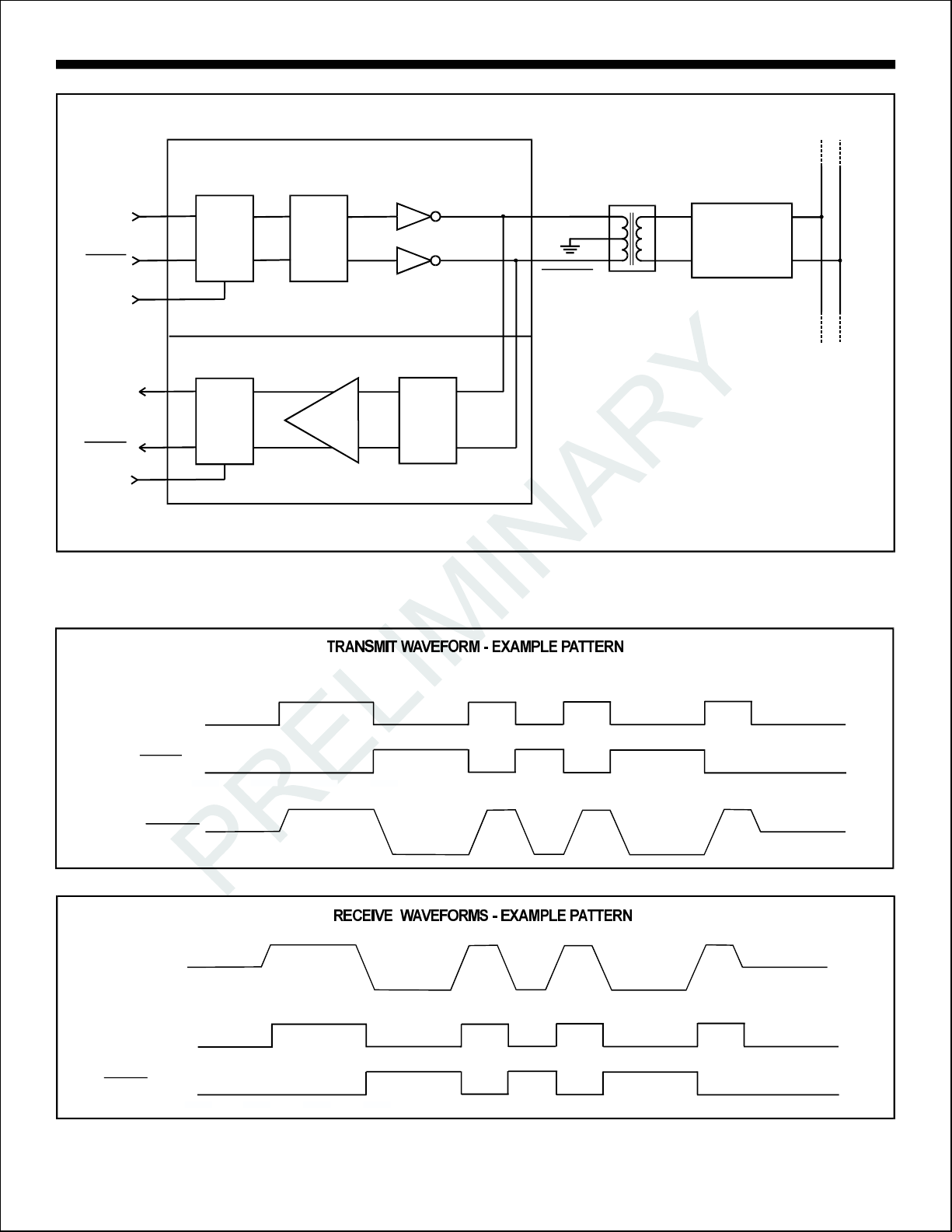
FUNCTIONALDESCRIPTION
TheHI-1567familyofdatabustransceiverscontaindifferentialvoltagesourcedriversanddifferentialreceivers.
TheyareintendedforapplicationsusingaMIL-STD-1553
A/Bdatabus.Thedeviceproducesatrapezoidaloutput
waveformduringtransmission.
TRANSMITTER
Datainputtothetransmittersectionofthesedevicesis
fromthecomplimentaryCMOS/TTLinputsTXA/Band
.Thisproducesanominal30Vpeaktopeaksignal
TXA/B
acrossa140ohmload.Thetransmitterisconnectedtothe
busviaa1:2.5transformerwhosesecondaryisconnected
totwo52ohmisolationresisterswhichfeedtheterminated
7 0ohmbus.Thiswillproduceanominalvoltageonthebus
of7.5voltspeaktopeak.
Thetransmitterisautomaticallyinhibitedandplacedinthe
highimpedancestatewhenbothTXA/Bandareei-
TXA/B
theratalogic“1”orlogic“0”simultaneously.Alogic“1:”appliedtotheTXINHA/Binputwillforcethetransmittertothe
highimpedancestate,regardlessofthestateofTXA/Band
TXA/B
RECEIVER
Thereceiveristransformercoupledtothebusbya1:1
transformer.Itsdifferentialinputstagedrivesafilterand
thresholdcomparator.CMOS/TTLdataisoutputtedatthe
RXA/Bandpins.RXA/B
Thereceiveroutputscanbothbeforcedtoalogic"0"
(HI-1567)orlogic“1”(HI-1568)bysettingRXENAor
RXENBlow.
HOLTINTEGRATEDCIRCUITS
2
HI-1567,HI-1568
TXA/B
TXA/B
TXINHA/B
RXA/B
RXA/B
RXENA/B
EachChannel
TRANSMITTER
Transmit
Logic
RECEIVER
Receive
Logic
Slope
Control
Comparator
Figure1.BlockDiagram
Input
Filter
BUSA/B
BUSA/B
Isolation
Transformer
DataBus
Coupler
Network
Director
Transformer
TXA/B
TXA/B
BUSA/B- BUSA/B
Vin
(LinetoLine)
RXA/B
RXA/B
HOLTINTEGRATEDCIRCUITS
3

HI-1567,HI-1568
ABSOLUTEMAXIMUMRATINGS
Supplyvoltage(
Logicinputvoltagerange
VDD)-0.3Vto+7V
-0.3Vdcto+5.5V
RECOMMENDEDOPERATINGCONDITIONS
SupplyVoltage
VDD.......................................5V...±5%
Receiverdifferentialvoltage10Vp-p
TemperatureRange
Driverpeakoutputcurrent+1.0A
IndustrialScreening.........-40°Cto+85°C
Powerdissipationat25°C0.5W
ceramicDIL,derate7mW/°C
SolderTemperature275°Cfor10sec
Hi-TempScreening........-55°Cto+125°C
MilitaryScreening..........-55°Cto+125°C
NOTE:Stressesaboveabsolutemaximum
ratingsoroutsiderecommendedoperating
StorageTemperature-65°Cto+150°C
conditionsmaycausepermanentdamagetothe
device.Thesearestressratingsonly.Operation
atthelimitsisnotrecommended.
VDD=5.0V,V=0V,T=OperatingTemperatureRange(unlessotherwisespecified).SSA
PARAMETERSYMBOLCONDITIONMINTYPMAXUNITS
OperatingVoltageVDD4.7555.25V
TotalSupplyCurrentICC1NotTransmitting22mA
ICC2
ICC3
PowerDissipationPD1NotTransmitting0.4W
PD2
Min.InputVoltage(HI)VDigitalinputs2.01.4V
Max.InputVoltage(LO)VDigitalinputs1.40.8V
Min.InputCurrent(HI)IV=4.9V,Digitalinputs20µA
Max.InputCurrent(LO)IV=0.1V,Digitalinputs-20µA
Min.OutputVoltage(HI)VI=-0.4mA,Digitaloutputs2.7V
Max.OutputVoltage(LO)VI=4.0mA,Digitaloutput s0.4V
RECEIVER
InputresistanceRinDifferential20kohm
InputcapacitanceCinDifferential5pF
CommonmoderejectionratioCMRR40dB
InputLevelVinDifferential8Vp-p
InputcommonmodevoltageVICM-5.05.0V-pk
ThresholdVoltageVTH1MHzSineWave0.561.2Vp-p
TRANSMITTER(MeasuredatPoint“A”inFigure2)
OutputVoltage35ohmload7.09.0Vp-p
OutputNoiseVONDifferential,inhibited10.0mVp-p
OutputDynamicOffsetVoltageAcross35ohmload-9090mV
OutputresistanceRoutDifferential,nottransmitting10kohm
OutputCapacitanceCout1MHzsinewave15pF
(MeasuredatPoint“V”inFigure2)IN
IH
IL
IHIH
ILIL
OHOUT
IHOUT
Vout
Vdyn
Transmitonechannel@
50%dutycycle
Transmitonechannel@
100%dutycycle
Transmitonechannel@
100%dutycycle
140ohmload28.036.0Vp-p
Across140ohmload-360360mV
320340mA
570615mA
0.95W
HOLTINTEGRATEDCIRCUITS
4

HI-1567,HI-1568
VCC=5.0V,V=0V,T=OperatingTemperatureRange(unlessotherwisespecified).SSA
PARAMETERSYMBOLTESTCONDITIONSMINTYPMAXUNITS
RECEIVER
ReceiverDelaytDRFrominputzerocrossingtoRXA/Bor450nsRXA/B
ReceiverEnableDelay
TRANSMITTER
DriverDelaytDTTXA/B,TXA/BtoBUSA/B,BUSA/B150ns
Risetimetr35ohmload100300ns
FallTimetf35ohmload100300ns
InhibitDelaytDI-HInhibitedoutput100ns
(MeasuredatPoint“V”inFigure2)
(MeasuredatPoint“A”inFigure2)
IN
tREN
tDI-LActiveoutput150ns
FromRXENA/Brisingorfallingedgeto
RXA/Bor
RXA/B
40ns
TXA/B
TXA/B
TXINHA/B
V IN
TRANSMITTER
35 Ω
1:2.5
BUSA/B
BUSA/B
55 Ω
2.5:1
55 Ω
RXENA/B
Figure2.Testcircuit
55 Ω
55 Ω
35 Ω
RECEIVER
A
RXA/B
RXA/B
HOLTINTEGRATEDCIRCUITS
5

HI-1567,HI-1568
ORDERINGINFORMATION
HI-1567PSI020PINPLASTICESOIC-WB-40°CTO+85°CINOSOLDER
HI-1567PST020PINPLASTICESOIC-WB-55°CTO+125°CTNOSOLDER
HI-1567CD020PINCERAMICSIDEBRAZEDDIP-40°CTO+85°CINOGOLD
HI-1567CDT020PINCERAMICSIDEBRAZEDDIP-55°CTO+125°CTNOGOLD
HI-1567CDM020PINCERAMICSIDEBRAZEDDIP-55°CTO+125°CMYESSOLDER
HI-1567CDM-03020PINCERAMICSIDEBRAZEDDIP-55°CTO+125°CMYESSOLDER
HI-1568PSI120PINPLASTICESOIC-WB-40°CTO+85°CINOSOLDER
HI-1568PST120PINPLASTICESOIC-WB-55°CTO+125°CTNOSOLDER
HI-1568CDI120PINCERAMICSIDEBRAZEDDIP-40°CTO+85°CINOGOLD
HI-1 568CDT120PINCERAMICSIDEBRAZEDDIP-55°CTO+125°CTNOGOLD
HI-1568CDM120PINCERAMICSIDEBRAZEDDIP-55°CTO+125°CMYESSOLDER
HI-1568CDM-03120PINCERAMICSIDEBRAZEDDIP-55°CTO+125°CMYESSOLDER
Legend:
ESOIC-ThermallyEnhancedSmallOutlinePackage(SOICw/built-inheatsink)
WB-WideBody
HOLTINTEGRATEDCIRCUITS
6

20-PINPLASTICSMALLOUTLINE(ESOIC)-WB
(WideBody,ThermallyEnhanced)
PACKAGEDIMENSIONS
inches(millimeters)
PackageType:
24HEW
.0105±.0015
(.2667±.0381)
.296±.003
(7.518±.076)
TYP.
0°to8°
.4065±.0125
(10.325±.318)
.5035±.0075
(12.789±.191)
.050
TYP
(1.27)
TopView
.018
(.457)
20-PINCERAMICSIDE-BRAZEDDIP
SEEDETAILA
.033±.017
(.838±.432)
Heatsinkstudon
bottomofpackage.
.215
TYP.
(5.461)
.090±.010
(2.286±.254)
DETAILA
.0075±.0035
(.191±.889)
.300
TYP.
(7.620)
Bottom
View
ACKAGEYPEPT:
20C
.025
(.635)
.025
(.635)
Min..
Min..
(5.080MAX.)
.125MIN.
(3.175MIN.)
.200MAX.
1.000 ± .010
(25.400 ± .254)
.050TYP.
(1.270TYP.)
.085 ± .009
(2.159 ± .229)
.017 ± .002
(.432 ± .051)
HOLTINTEGRATEDCIRCUITS
7
.310 ±. 010
(7.874 ± .254)
.100 ± .005
(2.540 ± .127 )
.300 ±. 010
(7.620 ± .254)
.010 +. 002/ − .001
(.254 ± .051 /− .025)
 Loading...