


SERVICE MANUAL
VORSICHT:
Data contained within this Service
Verbesserungen
ä
ndern.
MANUEL D’ ENTRETIEN
WARTUNGSHANDBUCH
No. 0301
VTMX900ECT
VTMX900EUK
VTMX905EUK
VTMX905EVPS
VTMX910EUK
VTMX902EL
VTMX930EVPS
VTMX932EL
CAUTION:
Before servicing this chassis, it is important that the service technician read
the “ Safety Precautions” and “ Product Safety Notices” in this service manual.
ATTENTION:
Avant d’ effectuer l’ entretien du châassis, le technicien doit lire les
«Précautions de sécurité» et les «Notices de sécurité du produit» présentés
dans le présent manuel.
Vor Öffnen des Gehäuses hat der Service-Ingenieur die „ Sicherheitshinweise“
und „ Hinweise zur Produktsicherheit“ in diesem Wartungshandbuch zu lesen
.
VTFX2000ELN
VTFX940EVPS
VTFX940EUKN
VTFX940ENA
VTFX942ELN
VTFX940ELN
VTFX952ELN
manual is subject to alteration for
improvement.
Les données fournies dans le
présent manuel d’ entretien
peuvent faire l’ objet de
modifications en vue de
perfectionner le produit.
Die in diesem Wartungshandbuch
enthaltenen Spezifikationen
können sich zwecks
June 2000
1-6
Safety instructions
– Safety regulations demand that the set be restored to its
original condition and that components identical with the
original types be used.
Safety components are marked by the symbol
– All ICs and many other semi-conductors are susceptible to
electrostatic discharges (ESD). Careless handling during repair
may reduce life drastically. When repairing, make sure that you
are conneted with the same potential as the mass of the set via
a wrist wrap with resistance. Keep components and tools on
the same potential.
– A set to be repaired should always be connected to the mains
via a suitable isolating transformer.
– Never replace any modules or any other parts while the set is
switched on.
– Use plastic instead of metal alignment tools. This in order to
prelude short-circuit or to prevent a specific circuit from being
rendered unstable.
GB
!
Remarks
– The direct voltages and oscillograms ought to be measured
relative to the set mass.
EXCEPTION
At the power supply, the DC voltages and the oscillograms at
the primary side are measured to LIVE GND.
– The direct voltages and oscillograms mentioned in the
diagrams ought to be measured with a colour bar signal and
the picture carrier at 503.25 MHz (C25).
– The oscillograms and direct voltages have been measured in
RECORD or PLAY mode.
– The semiconductors, which are mentioned in the circuit
diagram and in the parts lists, are fully exchangeable per
position with the semiconductors in the set, irrespective of the
type designation of these semiconductors.
Sicherheitshinweise
– Die Sicherheitsvorschriften erfordern es, daß sich das Gerät
nach der Reparatur in seinem originalen Zustand befindet und
daß die zur Reparatur benutzten Ersatzteile mit den
Originalersatzteilen identisch sind.
Sicherheits-Bauteile sind mit der Markierung versehen
– Alle IC’s und Halbleiter sind empfindlich gegen elektrostatische
Entladungen (ESD). Unvorschriftmässige Behandlung von
Halbleitern im Reparaturfall kann zur Zerstörung dieser
Bauteile oder zu einer drastischen Reduzierung der
Lebensdauer führen. Sorgen Sie dafür, daß Sie sich im
Reparaturfall über ein Armband mit Widerstand auf dem
gleichen Potential, wie die Masse des Gerätes befinden. Alle
Bauteile, Werkzeuge und Hilfsmittel sind auf das gleiche
Potential zu legen.
– Ein zu reparierendes Gerät ist immer über einen
Trenntransformator an die Netzspannung anzuschließen.
– Bei eingeschaltetem Gerät dürfen keine Module oder sonstige
Einzelteile ausgetauscht werden.
– Zum Abgleich sind ausschließlich Kunststoffwerkzeuge zu
benutzen (keine Metallwerkzeuge verwenden). Dadurch wird
vermieden, daß ein Kurzschluß entstehen kann oder eine
Schaltung instabil wird.
D
!
Anmerkungen
– Die Gleichspannung und Oszillogramme sind gegen
Gerätemasse zu messen.
AUSNAHME
Beim Netzteil sind die Gleichspannungen und Oszillogramme
auf der Primärseite gegen Live GND gemessen.
– Die Gleichspannungen und Oszillogramme angeführt in den
Schaltbildern sollen unter folgenden Bedingungen gemessen
werden: Farbbalkensignal, Bildträger auf 503.25 MHz (C25)
– Die Oszillogramme und Gleichspannungen sind in RECORD
oder PLAY gemessen. Die in den Stücklisten aufgeführten
Bauteile sind positionsweise voll auswechselbar gegen die
Bauteile in dem Gerät, ungeachtet der etwaigen
Typenbezeichungen.
Avertissements
– Les normes de sécurité exigent qu’aprés réparation I’appareil
soit remis dans son état d’origine et que soient utilisées les
piéces de rechange identiques à celles spécifiées.
Les composants de sécurité sont marqués
– Tout les IC et beaucoup d’autres semi-conducteurs sont
sensibles aux décharger statiques (ESD). Leur longévité
pourrait étre considérablement écourté par le fait qu’aucune
précaution n’est prise à leur manipulation. Lors de réparations
s’assurer de bien étre relié au méme potential que la masse de
l’appareil et enfiler le bracelet serti d’une résistance de
sécurité. Veiller à ce que les composants ainsi que les outils
que I’on utilise soient également à ce potentiel.
– Toujours alimenter un appareil à réparer à travers un transfo
d’isolement.
– Ne jamais remplacer les modules ni d’autres composants
quand I’appareil est sous tension.
– Pour l’ajustage, utiliser des outils en plastique au lieu
d’instruments métalliques. Ceci afin d’éviter les court-circuits et
exclure I’instabilité dans certains circuits.
F
!
Observations
– La mésure des tensions continues et des oscillogrammes doit
se faire par rapport à la terre de l’appareil.
EXCEPTION
Sur l’unité d’alimentation la tension continue et l’oscillogramme
sont mesurés sur le côte primaire en Live GND.
– La mésure des tensions continues et des oscillogrammes
figurant sur le schéma doit se faire dans un signal de barre
couleur porteuse image sur 503.25 MHz (C25).
– Les oscillogrammes et tension sont mésurées en mode
RECORD ou PLAY.
– Les semi-conducteurs indiqués dans le schéma de principe et
à la liste des compostants, sont interchangeables par repère
sur ce chassis avec les semi-conducteurs de l’appareil quelle
que soit la désignation de type donnée sur ces semiconducteurs.
Veiligheidsinstructies
– Veiligheidsbepalingen vereisen, dat het apparaat in zijn
oorspronkelijke toestand wordt teruggebracht en dat
onderdelen, indentiek aan de oorspronkelijke, worden
toegepast.
De veiligheidsonderdelen zijn aangeduid met het symbool
– Alle IC’s en vele andere halfgeleiders zijn gevoelig voor
elektrostatische ontladingen (ESD). Onzorgvuldig behandelen
tijdens reparatie kan de levensduur drastisch doen
verminderen. Zorg ervoor, dat U tijdens reparatie via een
polsband met weerstand verbonden bent met hetzelfde
potentiaal als de massa van het apparaat. Houd componenten
en hulpmiddelen ook op ditzelfde potentiaal.
– Sluit een apparaat dat gerepareerd wordt altijd via een
scheidingstransformator aan op de netspanning.
– Verwissel nooit modules of andere onderdelen terwijl het
apparaat is ingeschakeld.
– Gebruik voor het afregelen plastic i.p.v metalen gereedschap.
Dit om mogelijke kortsluiting te voorkomen of een bepaalde
schakeling instabiel te maken.
NL
Opmerkingen
– De gelijksspanningen en oscillogrammen dienen gemeten te
worden ten opzichte van de apparaat aarde.
– De gelijksspanningen en oscillogrammen vermeld in de
schema’s dienen gemeten te worden met een
kleurbalkensignaal beelddraaggolf op 503.25 MHz (C25).
– De oscillogrammen en gelijksspanningen zijn in RECORD of
PLAY mode gemeten.
– De halfgeleiders, die in het pricipeschema en in de stuklijsten,
zijn vermeld, zijn per positie volledig uitwisselbaar met de
halfgeleiders in het apparaat, ongeacht de typeaanduiding op
deze halfgeleiders.
!

1-7
Avvertimenti
– Le prescrizioni di sicurezza richiedono che l’apparecchio sia
ricondotto alle condizioni originali e che siano usati ricambi
originali.
Componenti di sicurezza sono marcati con
– Tutti gli IC e semiconduttori sono sensibili a scariche
elettrostatiche (ESD). Noncuranze durante la riparazione di
semiconduttori possono danneggiarli o condurre ad una
riduzione drastica della durata. Durante la riparazione
assicurarsi di essere collegati allo stesso potenziale attraverso
un bracciale di protezione contro scariche elettrostatiche.
Inoltre tenere anche tutti i componenti e gli attrezzi a questo
potenziale.
– Apparecchi da riparare bisogna collegarli sempre via un
trasformatore isolante (separatore) alla tensione normale.
– Non scambiare moduli o altri componenti quando l’apparecchio
è in funzione.
– Per l’accordo usare soltanto attrezzi di plastica (non usare
attrezzi metallici). Cosí si evitano cortocircuiti e collegamenti
instabili.
I
!
Osservazioni
– Misurare le tensioni continue e gli oscillogrammi riferiendosi
alla massa dell’apparecchio.
ECCEZIONE
Le tensioni continue e gli oscillogrammi dall’alimentatore sono
misurati sulla parte primaria contro GND-Live.
– Le tensioni continue e gli oscillogrammi indicati negli schemi di
collegamento devono essere misurati secondo le condizioni
seguenti: segnale barre colore, portante dell’immagine su:
503.25 MHz (C25).
– Gli oscillogrammi e le tensioni continue sono misurati in
RECORD o PLAYBACK.
– I componenti indicati nelle liste sono intercambiabili con quelli
nell’apparecchio nonostante l’eventuale denominazione di
modelli.
Avisos
– Las instrucciones de seguridad exigen que después de la
reparación el aparato se encuentre en el estado original y que
las piezas de repuesto, utilizadas para la reparación, sean
idénticas a las originales.
Los componentes de seguridad estan marcados con
– Todos los IC y semiconductores son sensibles a descargas
electrostáticas (ESD). Un tratamiento no conforme a las
instrucciones de semiconductores en caso de reparación,
podría llevar a la destrucción de estos componentes, o a una
reducción drástica de la duración. Tenga cuidado de que, en
caso de reparación, estar al mismo potencial que la masa del
aparato, por una pulsera con resistencia. Ponga todos los
componentes, herramientas y recursos al mismo potencial.
– Para reparar un aparato hay que conectarlo siempre a la
alimentación a traves de un transformador de aislamiento.
– Cuando un aparato está en marcha no pueden ser cambiados
módulos u otras piezas de repuesto.
– Para los ajustes hay que utilizar exclusivamente herramientas
de plástico (nunca herramientas metálicas). Así se evitaran
cortocircuitos y circuitos inestables.
E
!
Notas
– Hay que medir las tensiones continuas y los oscilogramas
contra la masa del aparato.
UITZONDERING:
Bij het netgedeelte zijn de gelijkspanningen en oscillogrammen
aan de primaire kant tegen Live GND gemeten.
– Las tensiones continuas y los oscilogramas mencionados en
los esquemas tienen que ser medidos de manera siguiente:
señal barra de color portadora de imagen en 503.25MHz (C25)
– Los oscilogramas y las tensiones continuas son medidas en
„RECORD“ y „PLAYBACK“
– Los componentes mencionados en las listas se los puede
cambiar por los componentes en el aparato, a pesar de
eventuales designaciones de tipos.
1-8
Modifications
Description of the system used for publishing
modification data and supplements to the
service manual.
All modification data and supplements to the Service Manual are
published by means of Service Information bulletins.
Each Service information has a number, for example :
VR 00 - 01 GB
Language
Sequence number
Y ear
Video cassette recorder
A Service Information bulletin concists of a front sheet, as the case
may be followed by supplementary and/or replacement sheets.
Replacement sheets serve to replace existing sheets in the Service
Manual. These sheets are identified by an additional letter after the
page number, for example 5-1a. Page 5-1a then takes the place of
page 5-1.
Supplementary sheets are inserted between the existing sheets in
the Service Manual. These sheets can be identified by an additional
figure following the page number, for example 5-1-1.
Sheet 5-1-1 should be inserted after page 5-1.
Description of the system by means of which
modifications are indicated in the recorder.
All important parts of the recorder, such as tape deck, p.c. boards
and modules, are provided with a sticker. These stickers specify a
number of product data. The meaning of this data will now be
explained for the most important sections.
Tape deck
12345678 009271 AT-P2/0 00151 10WD51
Production code
Factory indication
Production date
T ape deck type
Factory code number
Serial number
Note :
The production code and the serial number on the tape deck need
not correspond to the production code and the serial number on the
type plate.
Printed panels
The stickers are generally located on the track side of the module.
Example :
AVR 01102
12345 KW 015 WD 01 123456
Serial number
Production code
Production week
Printed board name
Factory code
Remarks :
The complete recorder
The type plate is located at the back of the recorder, below an
example of such a type plate is given.
Type plate :
.FOR BY GEMSTARDEVELOPMENT CORP.
P
D
D
R
E
IE
.GEMSTARDEVELOPMENT CORP.
O
MADE IN EUROPEMADE IN EUROPE
220-240 V ~220-240 V ~
AAA BBB CCC DDD EEE FFF GGG
AA
S
MODEL NO:MODEL NO:
PROD.NO:PROD.NO:
VN 37 0015 123456VN 37 123456
50Hz50Hz
VR110/02
Note :
- In the case of an important modification to the recorder the
production code on the type plate is increased by one.
E.g. 37 becomes 38.
- In the case of an important modification to the service
documentation the evolution code on the type plate is increased
by one.
E.g. AA becomes AB.
R
P
L
C
U
P
R
T
T
P
O
C
N
A
C
A
E
M
T
K
F
M
Service
O
N
R
U
P
R
E
A
N
F
O
A
M
M
L
Option codes (A-G)
E
P
E
E
S
O
D
V
N
L
IS M
A
E
E
E
Evolution code
R
D
M
V
IC
E
E
R
L
T
AT
D
A
R
S
T
E
R
Y
S
IS
Type number
D
A
S
M
T
W
N
E
S
W
UNDER LICENSE FROM
U
IE
M
G
IE
V
E
Y
V
W
G
B
W
O
O
R
H
H
S
SHOWVIEW IS A TRADEMARK APPLIED
O
S
SHOWVIEW SYSTEM IS MANUFACTURED
F
Serial number
Production date
Production center (VN),
Production code
The production code number will not always be mentioned.
In case of an important modification, the last figure of the factory code
number (point number) is increased by one. E.g. 6635.1 becomes
6635.2.
GB

1-9
GB D
F
TECHNICAL DATA TECHNISCHE DATEN CARACTERISTIQUES
Mains voltage.................................. Netzspannung ...................................... Tension secteur ............................. 220 - 240 V, +/- 10%
Mains frequency ............................. Netzfrequenz ....................................... Fréquence...................................... 45 - 65 Hz
Power consumption: ...................... Leistungsaufnahme:.............................. Puissance absorbée: ..................... mono 12.5 W during operation
HiFi 16 W during operation
without Low Power Standby...... Standby................................................ mode veille normal ........................ mono 4 W during standby
HiFi 4.4 W during standby
with Low Power Standby ........... Standby mit geringem Verbrauch ........ mode veille faible consommation .. < 4 W standby
Ambient temperature ...................... Raumtemperatur .................................. Température ambiante .................. +10°C to +35°C
Relative humidity ............................ Relative Luftfeuchtigkeit ...................... Humidité relative ............................ 20 - 80 %
Dimensions ..................................... Abmessungen ...................................... Encombrement .............................. 380 x 260 x 94 mm
Weight............................................. Gewicht ................................................ Poids .............................................. 3,7 kg
Fast forward/rewind time (turbo) ... Vor-/Rückspulzeit (turbo) ..................... Temps (re-)bobinage (turbo) ......... typ. 100s (E180 cass.)
Position of use ................................ Betriebslage ......................................... Position d'emploi ........................... horizontally, max. 15°
Video resolution .............................. Video-Auflösung .................................. Puissance absorbée ...................... ≥240 lines
Audio............................................... Audio.................................................... Audio SP: Linear Audio ................. 80Hz - 10kHz (+/−6 dB)
Audio LP: Linear Audio.................. 80Hz - 5kHz (+/−6 dB)
Stereo FM Audio............................ 20Hz - 20kHz (+/−3dB)
NL E I
TECHNISCHE GEGEVENS DATOS TECNICOS DATI TECNICI
Netspanning.................................... Tensión de red ..................................... Tensione di alimentazione............. 220 - 240 V
Netfrequentie .................................. Frecuencia de red ................................ Frequenza di rete .......................... 45 - 65 Hz
Opgenomen vermogen: .................. Consumo de potencia:......................... Potenza assorbita: ......................... mono 12.5 W during operation
HiFi 16 W during operation
zonder Low Power Standby ...... sin standby de bajo consumo .............. in attesa non a basso consumo .... mono 4 W during standby
HiFi 4.4 W during standby
met Low Power Standby ........... con standby de bajo consumo............. in attesa a basso consumo............ < 4 W standby
Omgevingstemperatuur .................. Temperatura ambiente ........................ Temperatura ambiente .................. +10°C to +35°C
Relatieve vochtigheid ..................... Humedad relativa ................................ Umiditá relativa .............................. 20 - 80 %
Afmetingen...................................... Dimensiones ........................................ Dimensioni ..................................... 380 x 260 x 94 mm
Gewicht ........................................... Peso ..................................................... Peso ............................................... 3,7 kg
Vooruit/terugspoeltijd (turbo) .......... tiempo de (re-)bobinado (turbo) .......... Tempo di (ri-)avvolgimento (turbo) typ. 100s (E180 cass.)
Gebruikspositie ............................... Posición de uso ................................... Posizione di funzionamento .......... horizontally, max. 15°
Opplossend vermogen ................... Resolución video ................................. Risoluzione video .......................... ≥240 lines
Audio............................................... Audio.................................................... Audio SP: Linear Audio ................. 80Hz - 10kHz (+/−6 dB)
Audio LP: Linear Audio.................. 80Hz - 5kHz (+/−6 dB)
Stereo FM Audio ............................ 20Hz - 20kHz (+/−3dB)
Euroconnector (AV1) SCART plug 1
Connection to TV, monitor, projection TV ...
Pin 1 ARO (audio right out) 500 mV
Pin 2 ARI (audio right in) 0,2 V
Pin 3 ALO (audio left out) 500 mV
Pin 6 ALI (audio left in) 0,2 V
Pin 7 Blue (out) **)
Pin 8 Switching output: (with R
low: 2 V
+/- 3 dB R
rms
to 2V
rms
+/- 3 dB R
rms
to 2 V
rms
= 10kOhm, C
load
rms
rms
1 kOhm
out
Rin 10 kOhm
1 kOhm
out
Rin 10 kOhm
< 2nF)
load
high: 9.5 V
rise time: 5 ms
Pin 11 Green (out) **)
Pin 15 Red (out) **)
Pin 16 Blanking (out) **) loop through enabled during
standby, view-mode
Pin 19 CVBS II (video out) 1 Vpp +1/-2dB R
Pin 20 CVBS I (video in) 1 Vpp +3/-3dB Rin 75 Ohm
75 Ohm
out
**) passive loop through from AV2
Cinch Audio/Video input on front panel (OPTION)
Audio:
AINFR (audio right in) red 0.2 V
AINFL (audio left in) white 0.2 V
Input impedance 47 kOhm
to 2 V
rms
to 2 V
rms
typ. 500 mV
rms
typ. 500 mV
rms
rms
rms
Video:
VFR yellow 1 Vpp + 3 / -3 dB
Input impedance 75 Ohm
Cinch Audio Out Rear (OPTION)
AOUT1R (audio right out) red 500 mV
AOUT1L (audio left out) white 500 mV
This outputs are in parallel with the corresponding outputs on
Euroconnector 1.
+/- 3 dB R
rms
+/- 3 dB R
rms
1 kOhm
out
1 kOhm
out
Euroconnector (AV2) SCART plug 2
Connection to decoder, SAT tuner, video disc, 2nd VCR ....
Pin 1 ARO (audio right out) 500 mV
Pin 2 ARI (audio right in) 0,2 V
Pin 3 ALO (audio left out) 500 mV
Pin 6 ALI (audio left in) 0,2 V
Pin 7 Blue (in) *)
Pin 8 Switching input only low: 2 V (low) Rin 10 kOhm
high: 4.5 V (high) R
Pin 11 Green (in) *)
Pin 15 Red (in) *)
Pin 16 Blanking (in) *) loop through enabled during
standby, view-mode
Pin 19 CVBS II (video out) 1 Vpp +1/- 2dB R
Pin 20 CVBS I (video in) 1 Vpp +3/-3 dB Rin 75 Ohm
*) passive loop through to Euroconnector AV1
+/- 3 dB R
rms
to 2 V
rms
+/- 3 dB R
rms
to 2 V
rms
rmsRin
rmsRin
1 kOhm
out
10 kOhm
1 kOhm
out
10 kOhm
10kOhm
in
75 Ohm
out
TUMOD
Modulator:
Frequency range loop through 45 MHz - 860 MHz
Gain: ANT IN - TV OUT 2 dB + 3 / -2 dB
ANT IN - TUN OUT 2 dB + 3 / -2 dB
Switch for RF input attenuation NO
Frequency range out (tuned by IIC bus) Ch 21 - Ch55
Tuner:
Frequency range 43 MHz - 860 MHz
for UK 450 MHz - 860MHz
Input voltage max. < 100 dBµV
min. > 60 dBµV

2-1
TOOLS FOR ERROR DIAGNOSIS
Replacement procedure for leadless
components (chip)
The following procedures are recommended for replacing leadless
components used in this unit.
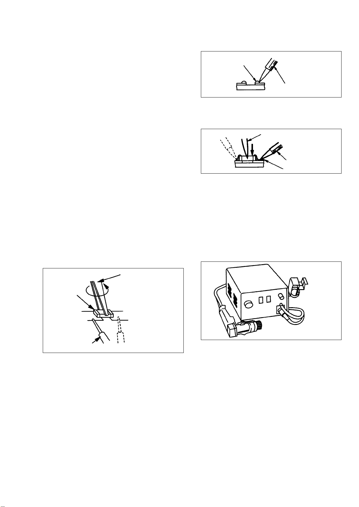
1. Preparation for replacement
a. Soldering iron
Use a pencil-type soldering iron that uses less than 30W.
b. Solder
Use Eutectic solder
(Tin 63%, Lead 37%)
c. Soldering time
Maximum 4 seconds.
Note:
a. Leadless components must not be re-used after removal.
b. Excessive mechanical stress and rubbing of the component
electrode must be avoided.
2. Removing the leadless components
Grasp the leadless component body with tweezers and alternately
apply heat to both electrodes. When the solder on both electrodes
has melted, remove leadless component with a twisting motion.
Note:
a. Do not attempt to lift the component off the board until the
component is completely disconnected from the board with a
twisting motion.
3. Installation of leadless components
a. Presolder the contact points on the circuit board.
Presolder
Soldering iron
Fig. 2-2
b. Using tweezers press down the part and solder both electrodes
as shown below.
Tweezers
Soldering iron
solder
Fig. 2-3
Note:
Do not glue the replacement component to the circuit board.
How to remove/install the FLA T PACK IC
1. How to remove the Flat Pack IC
• Using a hot air Flat Pack IC unsoldering equipment
b. Be careful not to break the copper foil on the printed circuit
board.
Tweezers
Chip
Soldering iron
Fig. 2-1
EXAMPLE
Fig. 2-4
GB

2-2
a. Prepare the hot air Flat Pack IC unsoldering equipment. Then
apply hot air to Flat Pack lC for 5 - 8 seconds.
b. Remove the Flat Pack lC with tweezers while applying the hot
air.
CAUTION:
To avoid damage, do not apply the hot air to the chip parts around
the Flat Pack lC for long periods.
C.B.A.
Masking
tape
Tweezers
Fig. 2-5
Put masking tape around the Flat Pack lC to protect adjacent parts.
2. The Flat Pack IC is fixed to the P.C.B. with glue; therefore take
care not to break or damage any foil under the lC or on each pin
when removing it.
Hot air Flat Pack
IC unsoldering
equipment
FLAT PACK IC
b. Lift up each lead of the Flat Pack IC individually, using a sharp
pin or non-solder wire (iron wire), while heating the pins using a fine
tip soldering iron or a hot air blower.
Sharp pin
Soldering iron
Fig. 2-7
• Using iron wire
a. Use unsoldering braid to remove the solder from all pins of the
Flat Pack IC. Apply solder flux to all pins of the Flat Pack IC, to
allow easy removal.
b. Affix the wire to workbench or solid mounting point (see Fig. 2-8)
c. Pull up the wire as the solder melts in order to lift the IC lead from
the P.C.B. contact pad, while heating the pins using a fine-tip
soldering iron or hot air blower.
• Using a soldering iron
a. Use unsoldering braid to remove the solder from all pins of the
Flat Pack IC.
Apply solder flux to all pins of the Flat Pack IC, to allow easy
removal.
FLA T P ACK
IC
Unsoldering
braid
Soldering iron
Fig. 2-6
Hot air
blower ...
Pull up gently
to remove
Fig. 2-8
Note:
When using a soldering iron care must be taken to ensure that the
Flat Pack lC is not held by glue or the P.C.B. may be damaged if
force is used.
If the IC is glued, heat the IC with hot air to loosen the glue.
Solid mounting
point
Iron wire
... or soldering iron
GB
2-3
2. How to install the FLA T PACK IC
a. Use unsoldering braid to remove the solder from the foil of each
pin of the Flat Pack lC on the P.C.B. in order to install the
replacement Flat Pack IC more easily.
b. The “•” mark on the Flat Pack IC indicates pin 1.
Make sure this mark matches the 1 on the P.C.B. when positioning
for installation. Then pre-solder the four corners of the Flat Pack IC.
(see Fig. 2-9).
EXAMPLE
Pin 1 on FLAT PACK IC is marked by a "•".
Fig. 2-9
Presolder
Soldering iron
C.B.A.
FLA T P ACK
IC
V oltage measurements
Color bar signal in SP REC and PB modes.
Note:
Voltage indications for the REC. and PB mode on the schematic
diagrams are shown below:
REC. and PLAY mode
(Identical voltages for
both modes).
PLAY mode
REC. mode
Fig. 2-11
How to read wave forms
1 Connecting point
2 Amplitude
3 Time base
4 Operating mode of the VCR
4
Fig. 2-10
c. Solder all pins of the Flat Pack IC. Make sure that none of the
pins have solder bridges between pins on the Flat Pack IC.
Note
All integrated circuits and many other semiconductor devices are
electrostatically sensitive and therefore require the special
handling techniques described in the “SAFETY INSTRUCTIONS”
section of this manual.
2
1
Fig. 2-12
3
Voltage indication of Zener diodes
The Zener voltage of Zener diodes is indicated as such on
schematic diagrams:
Example:
BZX79C20............Zener voltage: 20 Volts
GB
2-4
How to identify connectors on schematic
diagrams
Each connector is labeled with a connector number and a pin
number indicating to what component it is connected; in other
words, its counterpart.
Use the Connecting Wiring Diagram to find the connections
between associated connectors.
Example:
The connections between C.B.A.s are shown below:
Connector no.
and Pin no.
on PCB
PCB to which this
connector is connected
Test point information
With this model, test pin or components leads are used as contact
points for adjustment and checking. In case of other test points
with no test pin or components leads, use the foil solder pad to
connect the measuring equipment.
Removal or installation of flat cables
a. Removal
Pull out the flat cable, holding it securely to avoid damaging
individual wires (see fig. 2-14).
Flat cable
PULL
Connector
Pin 1
Board
Fig. 2-13
Connector no. to which
the left connector is
connected
1
Fig. 2-14
b. Installation
1. Adjust the position of the flat cable so that the lines on the flat
cable align with the pins X of the trap connector (see fig. 2-14).
2. Align individual wires with its individual trap connector
hole. Then insert the flat cable wire into the trap
connector.
CAUTION: After installation, inspect the connection to
insure that individual wires are not bent or touching other
wires.
GB
Dismantling instructions
2-5
General guidelines for dismantling housing
components, electronic parts and the drive
mechanism
Always disconnect from mains before dismantling or
assembly.
Due to the supply voltages (hot circuit) on the primary
side of the switched-mode power supply, an isolating
transformer is required for the operation of the device.
The drive or the drive/motherboard unit must not be
pulled out by the cross struts!
Components placed below the tape deck has to be
inserted exactly.
The use of a regulating isolating transformer is
recommended for detecting faults around the power
supply.
All screws of the video recorder can be removed or
tightened with a 10* torx screwdriver .
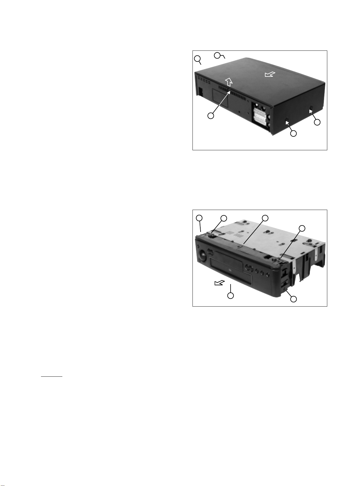
1. Housing cover (Fig. 1)
- Remove the four screws (A).
- Push catch (S) inwards, lifting lid at the same time to move out
of groove.
- Slide housing cover back by approx. 1 cm.
- Push centre of housing cover sides on underside approx. 1 cm
outwards and lift up the housing cover.
Assembly
Assemble in reverse order.
A
ä
Fig. 1
S
ä
S
ä
A
ä
A
A
S
S
S
ä
ä
2. Base plate (Fig. 2)
The base plate may not be removed from the frame!
3. Front panel (Fig. 2)
Preparation
Dismantle the housing lid as described in section 1.
- Position the device with the base plate facing upwards.
- Undo the six catches (S) one after the other, starting from the
left or the right.
- Remove the front panel by pulling it forwards.
- For devices with shuttle print or socket print, disconnect the
cabling to the motherboard.
Assembly
Assemble in reverse order (device in operational position).
Important
- The lift flap lever should be connected to the lift flap guide.
- Check that all catches are engaged.
Fig. 2
ä
S
ä
S
* …available from dealers
GB

2-6
4. Dismantling of the motherboard/drive
combination (Fig. 3) (Fig. 4)
Preparation
Remove the housing cover as described in section 1.
Remove the front panel as described in section 3.
- Move device into operational position (Fig. 3).
- Undo the two screws (B) of the stay and pull it up to remove it.
- Push back the lift by 5 cm after releasing both lift stops.
- Undo and remove the four fastening screws (C) of the drive.
- Detach the Cinch socket cable (K) and ground cable (M) from
the socket print (if present).
- Remove the cables (K1; K2; K3) from the guides on the rear of
the frame.
- Pull the Cinch socket holder with the socket and print up and
out of the frame (if present).
- Position the device with the base plate facing up.
- Undo the 8 catches (S) from the rear right to the rear front and
then from the rear left to the front left.
- After the weight of the motherboard/drive unit has released it
from the frame, the catch (S) at the mains socket has to be
released for a second time.
- The frame can be removed by lifting it off.
- Turn the motherboard/drive unit and move it into the service
position (Fig. 5), if necessary.
The device is operational in this position
”Eject” must NOT be used !!!
M/K
ä
B
ä
K1
C K2 K3
ä
ä
C
ä
ä
C C B
Lift protection
ä
ä
ä
Caution:
Adjustments can not be made in the service position.
”Eject” must NOT be used !!!
Assembly
- Position the frame with the top open onto a level surface.
- Hold the drive on the side at the lift and insert the motherboard/
drive unit into the frame, pushing it down lightly. Observe that
the power supply and Scart sockets are positioned in
openings.
- Check that all 8 catches (S) are engaged.
- Secure the drive with the four holding screws (C).
- Move the lift into the ”Eject” position.
- Push the stay onto the frame with the chamfered side facing to
the rear and secure with both screws (B).
- Insert the Cinch socket into the opening and ensure that it
engages.
- Connect the Cinch socket and the ground cable (K ; M)
(if present).
- Insert the cables (K1; K2; K3) into the supports provided in
the frame.
- Replace the front panel and the housing cover.
Fig. 3
ä
ä
ä
ä
SS
ä
GB
Fig. 4
ä
ä
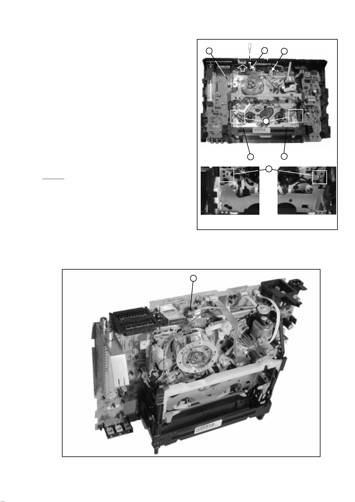
5. Dismantling the drive (Fig. 3)(Fig. 5)(Fig. 6)
Preparation
Remove the housing cover as described in section 1.
Remove the front panel as described in section 3.
- Undo the two screws (B) of the stay and pull it up to remove it.
- Push back lift by 5 cm after releasing both lift stops.
- Undo and remove the four fastening screws (C) of the drive.
- Undo and remove the ground screw (D) at the rear.
(For this purpose, insert the screwdriver through the hole in the
back panel).
- Remove the cables from the drive.
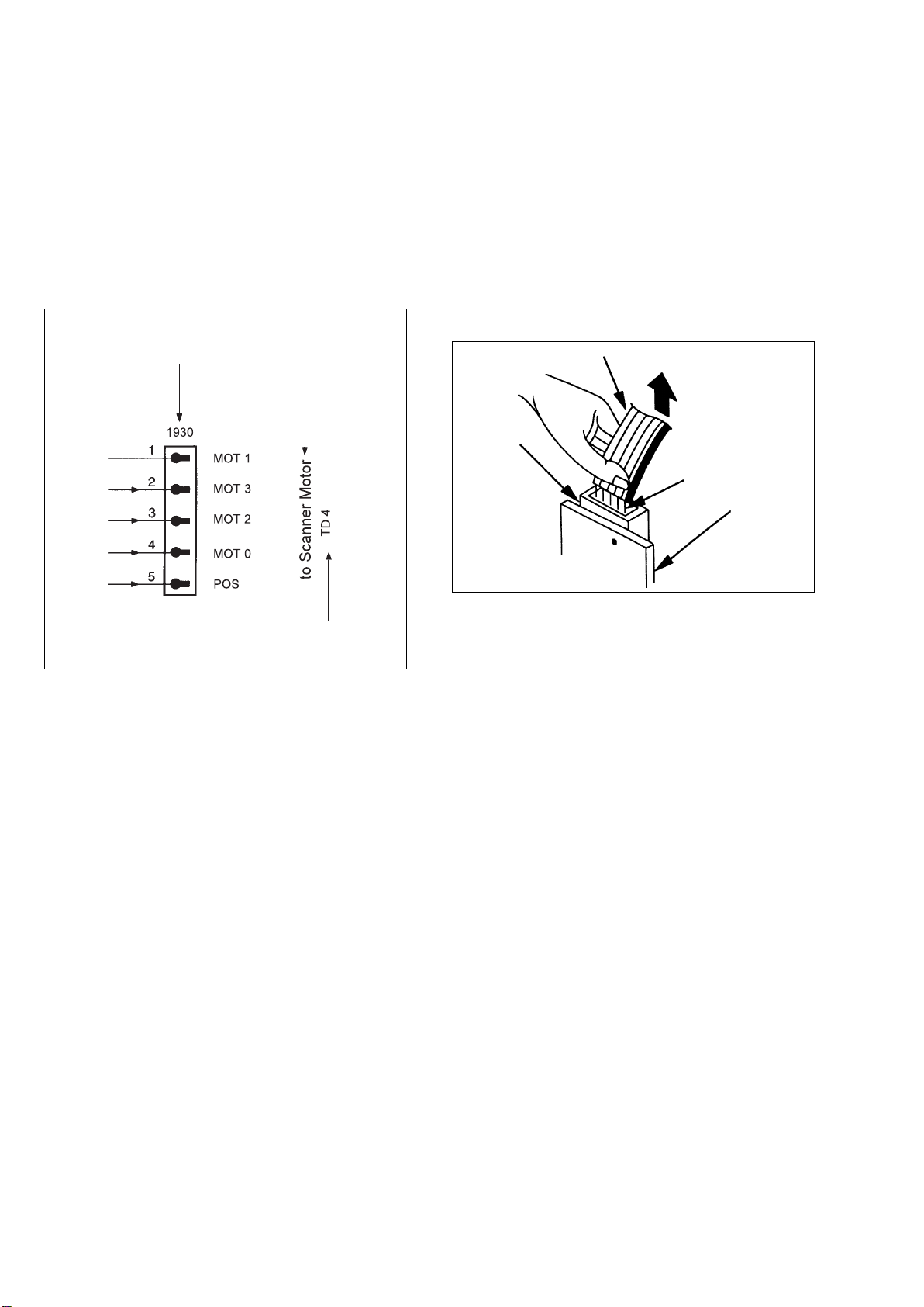
- Bend back the guard of the scanner cable.
- Remove the scanner cable from the socket.
- Return the lift into the ”Eject” position.
- Slightly lift the left rear side of the drive to undo the connector
to the capstan motor.
- Press both catches (S) together with fine pliers and lift the drive
around the snapholders.
- The drive may be separated from the motherboard.
Assembly
Assemble in reverse order.
Important
Observe that the cables (K1; K2; K3) are positioned in the
supports on the rear of the frame and that the ground
screw (D) is screwed in!
C
Fig. 6
ä
ä
C
2-7
D
C
S
ä
C
S
Fig. 5
Service position
D
ä
GB

2-8
Circuit descriptions
1. Switched-mode power supply PS (PS Part) ................................................................................................................................................9
1.1 Technical data:................................................................................................................................................................................................9
1.2 Functional principle: .......................................................................................................................................................................................9
1.3 Supply voltage part.........................................................................................................................................................................................9
1.4 Start-up with Mains-on: ..................................................................................................................................................................................9
1.5 Normal mode: .................................................................................................................................................................................................9
1.6 Overload, power limitation, burst mode: ......................................................................................................................................................10
1.7 Standby mode: .............................................................................................................................................................................................10
2. Operating unit DC (DC part) ........................................................................................................................................................................10
2.1 Evaluation of the keyboard matrix................................................................................................................................................................10
2.2 IR receiver and signal evaluation .................................................................................................................................................................10
2.3 Activation and function of the VFD display ..................................................................................................................................................10
3. Central Control AIO (AIO part) .................................................................................................................................................................... 11
3.1 Analogue interface to the µC:.......................................................................................................................................................................11
3.2 Tape end - LED control : ............................................................................................................................................................................... 11
3.3 CMT detection (video detection with CSYNC) ............................................................................................................................................. 11
3.4 EE-PROM ..................................................................................................................................................................................................... 11
3.5 Easy link (P50) .............................................................................................................................................................................................11
3.6 Shuttle: .........................................................................................................................................................................................................11
3.7 Satmouse...................................................................................................................................................................................................... 11
4. Deck electronics DE (DE part) ....................................................................................................................................................................11
4.1 CTL stage .....................................................................................................................................................................................................11
4.2 Power on reset (POR) generator ................................................................................................................................................................. 12
4.3 The sensor interface :...................................................................................................................................................................................12
4.4 Interface to the head drum motor driver part ............................................................................................................................................... 12
4.5 Interface to the loading motor driver part:....................................................................................................................................................12
4.6 Interface to the capstan motor .....................................................................................................................................................................12
5. Front end FV (FV part) .................................................................................................................................................................................13
5.1 The front end comprises the following parts : ..............................................................................................................................................13
5.2 The front end has been designed to receive the following systems:...........................................................................................................13
5.3 Tuner modulator (TUMOD) ...........................................................................................................................................................................13
5.4 IF selection ...................................................................................................................................................................................................13
5.5 IF demodulator .............................................................................................................................................................................................13
5.6 Audio demodulator .......................................................................................................................................................................................13
6. Video signal processing VS (VS part) ........................................................................................................................................................13
6.1 Switchover functions in the signal electronics IC LA71595M [7004]: ..........................................................................................................13
6.2 Recording : ...................................................................................................................................................................................................14
6.2.1 Luminance .................................................................................................................................................................................................14
6.2.2 Chrominance PAL......................................................................................................................................................................................14
6.2.3 MESECAM ................................................................................................................................................................................................14
6.2.4 SECAM L ...................................................................................................................................................................................................14
6.2.5 FM signal ...................................................................................................................................................................................................14
6.3. Playback: ..................................................................................................................................................................................................... 15
6.3.1 FM signal ...................................................................................................................................................................................................15
6.3.2 Luminance .................................................................................................................................................................................................15
6.3.3 Chroma PAL ..............................................................................................................................................................................................15
6.3.4 Chroma MESECAM...................................................................................................................................................................................15
6.3.5 Chroma SECAM L .....................................................................................................................................................................................15
6.3.6 NTSC .........................................................................................................................................................................................................15
6.3.7 PAL M,N.....................................................................................................................................................................................................15
6.4 General .........................................................................................................................................................................................................15
7. Audio linear (AL part)...................................................................................................................................................................................16
7.1 Audio I/O for the 1-scart version...................................................................................................................................................................16
7.2 Audio I/O for the 2-scart version...................................................................................................................................................................16
7.3 Audio linear recording...................................................................................................................................................................................16
7.4 Audio linear playback....................................................................................................................................................................................16
7.5 Audio linear muting.......................................................................................................................................................................................16
8. Audio HiFi - for stereo units (AF part)........................................................................................................................................................16
8.1 General .........................................................................................................................................................................................................16
8.2 Audio I/O .......................................................................................................................................................................................................16
8.3 Audio HiFi recording .....................................................................................................................................................................................16
8.4 Audio HiFi playback......................................................................................................................................................................................16
8.5 Interface to the audio linear..........................................................................................................................................................................16
9. IN/OUT (IO part) ............................................................................................................................................................................................17
9.1 Video:............................................................................................................................................................................................................17
9.1.1 Audio for the 2-scart version: ....................................................................................................................................................................17
9.2 Decoder mode: (REC or STOP)...................................................................................................................................................................17
9.2.1 Program position with decoder (front end)................................................................................................................................................17
9.2.2 External input with decoder .......................................................................................................................................................................17
10. Follow Me (FOME part) ..............................................................................................................................................................................17
11. VPS/PDC, on-screen display (VPO part) ..................................................................................................................................................17
11.1 VPS/PDC ....................................................................................................................................................................................................17
11.2 OSD-PART..................................................................................................................................................................................................17
GB

2-9
1. Switched-mode power supply PS (PS Part)
1.1 Technical data:
Mains voltage: 195-264 V
Maximum output: 15W / 40W (continuous / maximum output)
Operating frequency:40 kHz
Efficiency: approx. 75 % at maximum output
Six different direct voltages are supplied on the power supply
outputs.
1.2 Functional principle:
This power supply functions in a similar way to a blocking oscillator.
In the supply voltage part [1300 to 2318], the mains voltage is
rectified and buffered in the capacitor [2318]. From this direct
voltage [2318] energy is transferred into the transformer [5301,
pins 1-3] during the conductive phase of the switching transistor
[7302] and is stored there as magnetic energy. This energy is
passed to the secondary outputs on the power supply in the in the
blocking phase of the switching transistor [7302]. With the switchon time of the switching transistor [7302], the energy transferred in
every cycle is regulated in such a way that the output voltages
remain constant regardless of changes in the load or input
voltages. The power transistor is activated using the integrated
switch [7303] Fig.1.
1.3 Supply voltage part
The supply voltage part extends from the mains socket [1300] to
the capacitor [2318]. Using the diodes [6310, 6311, 6312 and 6313]
the a.c. supply voltage is rectified and buffered using the capacitor
[2318]. The line reactor [5305] and capacitor [2316] create a filter to
keep interference arising in the power supply away from the mains.
Components [1302], [3326] and [3323] protect the power supply
against short-term overvoltages in the mains, e.g. caused by
indirect effects from lightning.
MC44608
start - up
phase
200 µA
0
1
ISENSE
2
NC
7
VI
start - up
management
Vcc
management
switching phase
&
stand - by
200 µA
8
10
leading edge
blanking
rms
3318
C demag
latched off phase
start up phase
stand - by
management
+
65mV/45mV
&
PWM
comp
1
DEMAG
current mirror
current mirror
&
Fig. 1
OVP - out
1.4 Start-up with Mains-on:
Following connection to the mains, the capacitor [2310] is loaded
via the start-up resistor [3318] and a current source between pin 8
and pin 6 on the IC [7303]. Once the voltage on [2310] and
therefore the supply voltage Vcc on the IC [7303] has reached
approx. 13V, the IC starts up and issues pulses to its output on pin
5. These pulses are used to control the gate on the power transistor
[7302] (see Fig.2). The frequency has a fixed setting in the IC
(approx. 40 kHz). The current input on the IC is approx. 5 mA in
normal mode.
If Vcc drops to below approx. 10V (e.g. with power limitation) or if
Vcc exceeds around 15V (interruption of the control loop), the
output on the IC [7303, pin 5] is blocked. All output voltages on the
power supply, and therefore also Vcc, decrease. Once Vcc has
dropped to below approx. 6.5V, a new start-up cycle begins. (See
also “Overload, Power Limitation, Burst Mode“ section)
1.5 Normal mode:
With the power supply in normal mode, the periodic sequences in
the circuit are divided primarily into the conductive and blocking
phase of the switching transistor [7302]. During the conductive
phase of the switching transistor [7302], current flows from the
rectified mains voltage to the capacitor [2318] through the primary
coil on the transformer [5301, pins 1-3], the transistor [7302] and
resistors [3314, 3331] to earth (see Fig.1). The positive voltage on
pin 1 of the transformer [5301] can be assumed to be constant for a
switching cycle. The current in the primary coil on the transformer
[5301] increases linearly in the pattern of U=L*di/dt. A magnetic
field representing a certain volume of the primary current is formed
inside the transformer. In this phase, the voltages on the secondary
coils are polarised in such a way that the diodes [6300, 6301, 6306,
6308 and 6309] block. From the controller on [7301], a current is
supplied to the CTRL input on the IC [pin 3, 7303] via optocoupler
[7300]. Once the switch-on time for the switching transistor [7302]
has been reached, which corresponds to the current supplied on
the CTRL input, the switching transistor is switched off.
Once the switching transistor has been switched off, the blocking
phase begins. No more energy will be transferred into the
transformer. The inductivity of the transformer will still attempt to
maintain the current which has flowed through it (U=L*di/dt) at a
constant level. As the primary current circuit is interrupted by the
shut-off switching transistor [7302], the current will flow through the
secondary coils.
current and voltage
quick OVP
PWM
latch
stand by
UVL01
references
&
output
buffer
DRIVER
01
VCC
GND
CTRL
7300
6307
3314
7302
6304
+
6305
6
2310
5
4
3
t
regulation
block
200 µA
thermal shutdown
&
latch OFF phase
5301
GB

2-10
The polarity of the voltages on the transformer is reversed, which
means that the diodes [6300, 6301, 6306, 6308 and 6309] become
conductive and current flows into the capacitors [2301, 2305, 2309,
2311 and 2312] and the load. This current is also ramp-shaped (di/
dt negative, therefore decreasing).
The control adjustment for the switched-mode power supply is
made by changing the conductive phase of the switching transistor
(see Fig.2), so that either more or less energy is transferred from
the rectified mains voltage to [2318] in the transformer. The control
information is provided by the control element [7301]. This element
compares the 5V output voltage via the voltage dividers [3300,
3306, 3336] with an internal 2.5V reference voltage. The output
voltage from [7301] passes via an optocoupler [7300] (for the metallic isolation of the primary and secondary parts) as the current
value to pin 3 on the IC [7303]. The switch-on time for the switching
transistor [7302] is inversely proportional to the value of this
current.
1.6 Overload, power limitation, burst mode:
With an increasing load on one or more power supply outputs, the
switch-on time for the power transistor [7302] also increases, and
thus also the peak value of the delta-shaped current through this
power transistor. The equivalent voltage circuit for this current
profile is passed from resistors [3314] and [3331] via [3312] and
[3347] to pin 2 on the IC [7305]. If the voltage on pin 2 reaches 1V
in one switching cycle, the conductive phase of the switching
transistor is ended immediately. This check is made in each
individual switching cycle. This process ensures that no more than
approx. 48W can be taken out of the mains ( = power limitation ).
If the power supply reaches the power limit, the output voltages
and the supply voltage Vcc on pin 6 of the IC [7303] will be reduced
following further loading. If Vcc is less than approx. 10V at any point
during this process, the output on the IC [7303, pin 5] is blocked. All
output voltages and Vcc are reduced. Once Vcc has dropped to
below approx. 6.5V, a new start-up cycle begins. If the overload
status or short-circuit remains, the power limitation will be activated
immediately and the voltages will continue to be reduced, followed
by another start-up attempt ( Burst Mode ). The amount of power
taken up from the mains in burst mode is low.
1.7 Standby mode:
In the ‘Standby‘ operating mode on the device, the ’STBY‘ control
line is used to shut off the output voltages 14AL, 5VA and 5VD on
the power supply to minimise the amount of power taken up from
the mains. The supply to the display heating can also be switched
off using the ‘I1WSTBY‘ control line. The power supply itself will
continue to function continuously in the ‘Standby‘ operating mode
with a switching frequency of 40kHz.
U
3
= UGS
t
I
Dmax
point of reversal
t
UDS
I
D
t
Fig. 2
2. Operating unit DC (DC part)
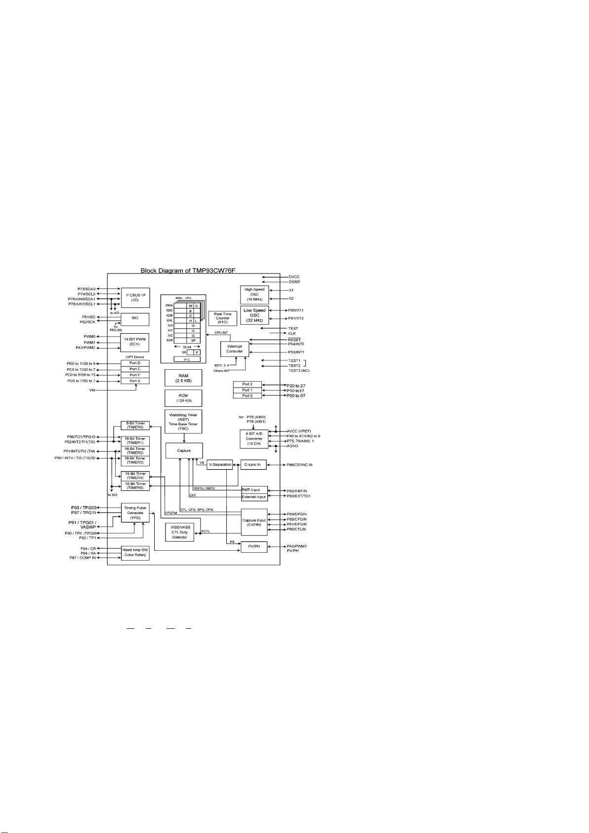
The microcontroller TMP93CT76F [7899-A] is a 16 bit
microcontroller fitted with 128Kb ROM and 2.5Kb RAM.
It is the core element of the operating unit, fulfilling the following
tasks with the respective functional groups:
• Integrated VFD driver
• Timer
• Evaluation of the keyboard matrix
• Decoding the remote control commands from the infra-red
receiver pos. 6170
• Activation of the display
• Back-up mode
In normal operation, the µP is operated in dual-clock mode, i.e.
both quartzes [1170, 1171] oscillate. The time is derived from the
slow quartz [1170] (32.768 kHz), and the fast quartz [1171]
(16MHz) is used to generate the system clock frequency.
In case of a mains failure (back-up mode) the µP is not reset, but
instead the mains failure is registered by the IPOR interrupt 3
[7899-B] (pin 67) and the µP is moved into “Sleep mode” (low
power consumption). The 16MHz quartz is turned off and the
32kHz quartz is then used as the clock and system clock frequency.
The operating voltage for the AIO is buffered by a back-up cell [pos.
2174, 2172]. A diode [6171] prevents this gold capacity from
discharging.
2.1 Evaluation of the keyboard matrix
There are 12 different keys. Each key function is assigned a fixed
voltage value. This value is decoded using an analogue/digital (A/
D) port (7899-B, pin 56). Each mechanical key position on the
printed board can adopt any key function via a coding resistor.
Pressing keys simultaneously may lead to undesired functions!
Schematic:
10K
DC-KEY
[7899-B, pin56]
100K
Y
C
B
E
T
R
S
2.2 IR receiver and signal evaluation
The IR receiver [6170] includes a selective, controlled amplifier in
addition to a photo-diode. The photo-diode changes the received
transmission (approx. 940nm) in electrical pulses, which are then
amplified and demodulated. On the output of the IR receiver [7220]
a level lift 0V/5V pulse sequence, which corresponds to the
envelope curve of the received IR remote control command, can be
measured. This pulse sequence is input into the controller for further signal evaluation via input IRR [7899-B, pin 46].
2.3 Activation and function of the VFD display
In principle, the VFD display [7170] is a tube triode in which the
heating filaments in the tube serve as cathodes (F+,F-). The 7 grids
(G1 - G7) are activated via PC2 - PC7, PD0 on the controller, and
the 16 anodes (P1 - P16) are controlled via ports PE0 - PE7, PF0 PF7, PC0, PC1 on the controller, each with a positive potential
compared to the cathode.
The grids and anodes (digits and symbols to be displayed) are
activated in the time-multiplex procedure, voltage lift 5V/-18V. A
dimmer function is generated using pulse-width modulation of the
grid control signals. At maximum display brightness, the pulse
width for each grid is 2.16 ms. It can be reduced, controlled using
software, which reduces the visual brightness of the VFD display
accordingly.
A digit or symbol is only illuminated if the corresponding anode and
the surrounding grid are switched simultaneously to 5V for a certain
time within a scanning period. The electrons emitted from the
cathode are accelerated by the positively charged grid and hit the
luminous layer of the anode which is also positively charged.
T
C
JE
T
27K
/E
47K
18K
12K
P
P
O
O
T
T
S
S
8K2
C
JE
E
D
Y
IN
LA
W
P
R
O
5K6
3K9
IT
N
W
O
E
M
R
1K2
2K2
470E
N
ILL
T
S
W
O
P
D
U
0E
GB
2-11
During the remainder of the scanning period, the corresponding
grid and parts of the anode are at -18V, due to the internal pulldown resistors in the controller. This potential is still lower than the
average cathode potential of approx. -15V, prevents the
acceleration of electrons, thus causing the relevant grid and anode
segments to go dark.
The heating direct voltage of the display (U = 3.5V) is supplied from
the power supply via lines HELO or HEHI to pins F+ and F- to the
VFD display. Resistors [3070] and [3071] restrict F- to approx. 15V.
3. Central Control AIO (AIO part)
The microcontroller (µC) TMP93CT76F [7899-B] includes the
following functions:
• PWM outputs
• A/D converters
• Composite sync input
• Special servo inputs for VCR functions
• I²C-BUS interface
• Shuttle evaluation
3.3 CMT detection (video detection with CSYNC)
This has been extended due to identification problems with weak
transmission signals and video signals not conforming to the
STANDARD (common channel interference). The CSYNC line is
supplied to the µP [7899-B] on pin 50. A hardware integration
[7807,7808,7809] of the video pulse compensates the interference
generated by the common channels and weak signals.
3.4 EE-PROM
The EE-PROM [7818] is a non-volatile memory which can be
erased and written to electrically. (Data remains
even if the operating voltage fails). Data specific to the device such
as the X distance, head changeover position, preset stations, optional bytes etc. is stored in the EE-PROM [7818].
The data is accessed by the µP via the I²C bus.
3.5 Easy link (P50)
For the communication between the TV set, video recorder and the
peripheral devices, a bi-directional single-wire bus is used, which
runs via pin 10 to scart socket 1.
The output signal is generated on pin 84 of the µC [7899-B], pin 68
is the signal input.
3.6 Shuttle:
The shuttle is connected to the motherboard on plug pos.1982. It is
a binary coded rotary switch with a rotation angle of +/- 70 degrees
and 16 switch positions. These are input and evaluated via four
lines (shuttle b1 – shuttle b4) to the input ports P24 – P27 [7899B
pins 2-5].
3.1 Analogue interface to the µC:
The following analogue levels are supplied to the µC’s
internal analogue/digital (A/D) converter:
• TAE/TAS Tape End / Tape Start Detection
• TRIV Tracking Information Video
• TRIA Tracking Information Audio
• AGC Automatic Gain Control
• AFC Automatic Frequency Control
• 8SC1/2 Pin 8 Scart1 or Scart2 switching voltage
• Key-in Keypad evaluation
3.2 Tape end - LED control :
The LED current is switched using transistor [7804]. The ON time is
approx. 1 msec and the OFF time approx. 12 msec during playback
and 1msec to 5.5msec during the winding functions.
The LED current is typically 150 mA. In order to prevent
interference from the relatively high pulsed current ‘spreading’
through the entire unit, the LED is fed from the 14VM1, and filtered
by 2 resistors [3800, 3805] with 10R each and a 220µF electrolytic
capacitor [2803].
3.7 Satmouse
For activating a sat-receiver via an external infrared electronic
transmission unit (Satmouse) a bi-directional data line, a shortcircuit proof +5V and earth are provided via a 3-pin 3.5mm jack
[1941].
The +5V is limited to approx. 140 mA using a current limiting switch
[7812 and peripherals].
4. Deck electronics DE (DE part)
The deck interface IC MP63100FP [7463] contains the
following functional groups:
• CTL stage (tape synchronisation)
• Sensor interface
• Power on reset
• Head drum motor driver
• Loading motor driver
• Capstan motor control
4.1 CTL stage
The IC M63100FP [7463] contains a read/write stage for the CTL
track with the option of overwriting an existing CTL track without
any interference. The playback stage is fitted with a “digital” fivestage AGC. This logic circuit identifies the size of the output signal
supplied by the CTL head, and then selects the best amplification
ratio in the playback stage using comparators.
The CTL head voltage can therefore vary greatly, if Vmax / Vmin is
great. The slowest tape speed is in LP mode. The fastest speed is
adjusted during rewind. To ensure that the duty cycle in the tape
sync is always reproduced correctly in the conditions mentioned
above (important for detecting VISS marks), the amplifier must not
be overdriven.
The five-stage AGC alone cannot cover the large dynamic range of
the input voltage. The amplifier is therefore also equipped with a
low pass characteristic (fg = 3kHz typ.; internal).
GB

2-12
In parallel with the CTL head is the RC cell comprising capacitor
[2479] and resistor [3471]. The capacitor [2479], together with the
CTL head inductivity, causes a resonance step-up at around 10
kHz and the resistor [3471] suppresses this step-up. This creates
an aperiodic transient response in the resonance. Beyond the
resonance frequency , there is an adjustment in terms of a steep fall
in the frequency transmission characteristic. This effectively
suppresses high-frequency pick-ups. The CTL head signal
amplitude in standard play is around 1mVp (typ.) which means that
the amplification for the playback amplifier must be
correspondingly high. To avoid offset problems, a 100 µF
electrolytic capacitor [2490] is fitted in the negative feedback
branch for DC decoupling.
The polarity of the playback amplifier can be changed using the
Video Index Search System (VISS) voltage. This is the only way in
which the µP can write a VISS mark on the tape without spikes. The
Write/Read (W/R) signal is used to switch over between record and
playback:
W = “H“, R = “L“.
4.2 Power on reset (POR) generator
The POR generator contained in the M63100FP [7463] requires
only one external capacitor [2477], which specifies the length of the
POR pulse. For 33 nF, tPOR is approx. 30ms.
The response threshold of the reset circuit is between 4.5 and 4.8
V. Supply fluctuations which are shorter than tPOR/100 area and
which do not fall below 4.0 V, do not trigger the POR. The µP is
reset using the inverted POR.
4.3 The sensor interface :
The four comparators in the M63100FP [7463] are used to convert
sensor signals to the logic level. The outputs are overload
protected by a current limiter and thermal overload protection. Only
the non-inverting input on each comparator is accessible from the
outside. The other inputs are connected to an internal reference of
2.5V. The fixed hysteresis of the comparators of approx. 18 mV is
also located internally.
The comparators are connected as follows:
Comparator 1: In = FTA, pin 39; Out = FTAD, pin 34:
FTA
= threading tachometer. This signal comes from a forked light
barrier in the deck. An infra-red light beam is interrupted by a 4blade impeller (butterfly). The output amplitude for the light barriers
should be less than 2V for the low level and greater than 3V in the
high level to ensure a correct evaluation process. An additional
hysteresis is created with a resistor [3476]. For unit versions <1W
and FOME the external operation amplifier [7530B] is used to
reduce the power consumption in <1W mode.
Comparator 2: In = WTR, pin 38; Out = WTRD, pin 33:
WTR
= Winding tachometer right, from a reflection photoelectric
barrier. The level is the same as for the FTA.
Comparator 3: In = WTL, pin 37; Out = WTLD, pin 31 :
WTL
= Winding tachometer left, from a reflection photoelectric
barrier. The level is the same as for the FTA.
Comparator 4: In = FG, pin 35; Out = FGD, pin 30:
FG
= capstan tachometer. This signal stems from an amplifier for
the tachometer hall sensor on the motor unit [1946 pin 4]. The
output impedance is 10 kOhm. The amplitude of the virtually
sinusoidal signal is normally 1 Vp. It should not fall below 300
mVpp. It is AC-coupled via a capacitor [2485]. In order for a bias
current to flow, the input pin 31 must be passed via a resistor [3474]
to the reference voltage on pin 4. A capacitor [2480] for filtering out
high-frequency interference is arranged in parallel to the bias
resistor.
4.4 Interface to the head drum motor driver part
The head drum control voltage (speed and phase control
information) is output via a µP-output (7899-B pin 35; PWM 14-bit).
This pulse-wide modulated signal is fed to the motor driver IC
M63100FP [7463 pin 11] and integrated with the capacitor [2469].
This IC already has a completely integrated ‘start-up’ circuit fitted.
For the commutation, the head drum motor driver uses the e.m.f.
on the non-current carrying motor coil (transformer principle). The
motor speed is also discharged from there at the same time. The
phase of the head disc is discharged from a position coil. The
speed and phase are multiplexed into one signal [7463 pin 6] and
output, which means that the falling edge of the signal is available
with a positive edge for the speed (FG/450Hz) and at 25Hz for the
position pulse (PG).
The motor driver M63100FP [7463] is connected to the head drum
motor on the motherboard using plug [1948].
• DRUM is the speed-phase control signal. The resolution is
14 bit.
• PG/FG is the combined POS/tachometer signal from the
M63100FP [7463].
4.5 Interface to the loading motor driver part:
The loading motor driver part is constructed for use as a bridged
dual power operations amplifier (OPAMP). It can supply max. +/-
0.8A output current. The output current is limited to approx. 0.7A by
the internal resistance of the loading motor (18 Ohm typ.) (start-up
or motor is blocked).
Between the IC outputs [7463, pins 22 and 24] there is a
“Boucherot” circuit [3467] 1E, [2474] 100 nF for suppressing a
spurious 3MHz oscillation from the output stage. One half of the
bridge is controlled via the TMO line on pin 27 and acts as a
comparator. The other half is an amplifier integrator with a 3.9 gain.
A change in the input voltage (THIO) of between 0 and 5V on pin 25
results in a change in the output voltage of between 0V and almost
Ub. With 50% modulation (THIO = 2.5 V) pin 24 has approx. 7 V.
The 100nF capacitor [2473] in the negative feedback of the op-amp
filters out the PWM frequency of approx. 39kHz. During POR, the
µP issues “L” to the THIO line, whilst TMO is “H”. This ensures that
no current flows in the motor for the duration of the POR pulse. This
prevents the motor being destroyed in case of prolonged running or
blockage. This arrangement also has a disadvantage, however.
This is that if the 5 V supply fails (e.g. because the 5V fuse has
blown), residual voltages may be passed to the IC inputs via the
adjacent 14 V voltages. These residual voltages trigger the
comparator and the op-amp in opposite ways, causing a shortcircuit in the blocked loading motor after about a minute. To get
around this problem, a separate voltage divider is used internally
for the comparator. Both outputs on the M63100FP [7463] are then
in “common mode” if this error occurs.
4.6 Interface to the capstan motor
The driver IC on the capstan motor is activated via connector
[1946].
CAP is the signal for the capstan speed. This voltage may vary
without load between 0 and 5 V.
The rotational direction of the motor is determined using CREV
(capstan reverse). The maximum current input for the motor is
limited to 1A. Typical values in PLAY mode are 0.2 ... 0.3 A.
GB

2-13
5. Front end FV (FV part)
5.1 The front end comprises the following parts :
• TUMOD = Tuner (+ Modulator Option) (+Booster Option)
(+Passive Loop Through Option)
• IF amplifier & video demodulator IC TDA 9817, [7705] with FM
- PLL demodulator
• IF amplifier & video demodulator IC TDA 9818, [7705] with FM
- PLL and AM demodulator
• FM stereo decoder TDA 9873 [7760]
• Multi-standard FM stereo, AM, NICAM decoder MSP3415D
[7761]
5.2 The front end has been designed to receive
the following systems:
• PAL B/G with FM stereo
• PAL 1 or PAL BG with NICAM stereo
• PAL BG with NICAM and FM stereo
• PAL BG/I SECAM L/L’ with NICAM and FM stereo
• PAL BG SECAM DK with NICAM and FM stereo
• PAL B/G =/01,/02/16
• PAL I =/05 Pal I with UHF reception
• PAL I Ireland =/07 Pal I with VHF/UHF reception
• SECAM L,L‘, PAL BG/I =/39
• PAL B/G, SECAM DK =/58
The relevant layout is given in the version list on the circuit diagram.
5.3 Tuner modulator (TUMOD)
The tuner and modulator are fitted into the same housing.
Both the tuner and the modulator are PLL-controlled. The reception
frequency or modulator frequency is set using the IIC bus.
The amplification is determined by the AGC voltage at pin 5 [1701]
(for operation, see IF demodulator section).
5.4 IF selection
The IF frequency of the video carrier is 38.9 MHz for all systems
except SECAM L’ (33.9 MHz).
For PAL BG-SECAM DK and for PAL BG/I-SECAM L/L´ a quasisplit audio system is used; i.e. for video and audio carriers, separate surface-wave filters (OFW) are required [1704, 1703]. For all
other standards an intercarrier system is used; i.e. a common OFW
with audio stair-step can be used [1704] for video and audio
carriers.
For the PAL BG/I-SECAM L/L’ version, an additional circuit for
suppressing the adjacent channel audio carrier is provided, which
is set using coil [5704] to maximum suppression at 40.4MHz.
5.5 IF demodulator
TDA 9818
The IF signal from the tuner is processed by another demodulator
IC of type TDA 9818 [7705]. The TDA 9818 is used to demodulate
pos. or neg. modulated video carriers. It is possible to generate a
QSS-audio-IF signal or an intercarrier IF signal for demodulation in
the audio demodulator [7761]. For the best possible video signal
performance the IF signal is conveyed via an OFW [1704]
according to the standard. The audio-IF carrier is selected in the
audio OFW [1703] which is switched for SECAM L’. The output
signal for this OFW is further processed in the TDA 9818. FM
carriers are converted from the IF level into the audio IF position
and further processed in the audio demodulator. The AFC coil
[5702] on the TDA 9818 is adjusted so that when a frequency of
38.9 MHz is supplied to the IF output of the tuner, the AFC voltage
on pin 17 on the TDA 9818 is 2.5V. The setting of the picture carrier
frequency for SECAM L in the TDA 9818 is achieved by connecting
pin 7 of the IC via a potentiometer [3730] to earth. The AFC voltage
on pin 17 TDA 9818 should then also be 2.5V at 33.9 MHz. The HFAGC is set using the AGC controller [3707] so that with a
sufficiently large input signal (74 dBµV), the voltage at the IF output
on the tuner [1701, pin 17] is 550 mVpp. The setting must be
carried out when the audio carrier is switched off. The demodulated
video signal appears on pin 16 [7705]. The video drop [1705]
reduces adjacent channel sound carrier and sound carrier
remainders in the video.
TDA 9817
As for TDA9818, without the option for processing AM audio and
positive video modulation (SECAM L,L’).
5.6 Audio demodulator
Multi-standard audio processor MSP 3415D
The MSP 3415D [7761] is a multi-standard sound processor which
can demodulate FM Mono/Stereo, NICAM and AM signals. The
incoming signal is first controlled and then digitised. The digital
signal is then demodulated in 2 separate channels. In the first MSP
channel, FM and NICAM (B/G/I/D/K) are demodulated, whereas in
the second MSP channel, FM and AM is demodulated again
(NICAM L corresponds to NICAM B/G). These demodulated
signals are selected digitally in the I/O and switched to the D/A
converter on the outputs. Amplitude and bandwidth of the
demodulated audio signals can be determined in the MSP using
the corresponding commands via the I2C bus. This means that the
setting required for the best possible performance can be made.
FM stereo audio decoder TDA 9873
The TDA 9873 [7760] is a multi-standard A2 audio processor which
can demodulate FM mono/stereo signals. The audio IF SIF2 is
passed from pin 3 [7705] to pin 25 [7760]. The demodulated stereo
signals AFL and AFR I2C bus are available controlled on pins 1 and
2.
6. Video signal processing VS (VS part)
6.1 Switchover functions in the signal electronics
IC LA71595M [7004]:
The signal electronics IC LA71595M [7004] are controlled via the
I2C Bus on pins 23 and 24 by the AIO.
As groups 5 and 6 can only be transferred with a change in HP1, it
must be ensured that during measurements the HP1 line is always
connected to the SE IC or replaced by a corresponding signal.
REC/PB via IIC bus
During RECORD pin 30 must be passed via [7009] on 5V
(IREV=LOW) to activate the video write current stages. T o keep the
transient condition of the write current as short as possible, the
signal electronics IC is set to REC via IIC bus before the pin 30
change.
PAL/SECAM/MESECAM/NTSC via IIC bus
SP/LP/SLP via IIC bus
VIDEO INPUT SELECTOR SWITCH via IIC bus
In 1-scart units a distinction is made via the IIC bus between VFV
(pin 36 / VID2) and VBS which corresponds to VIN1 (pin 38 / VID1).
In 2-scart units the video input selection is made via IIC bus in the
STV6401 [7904] and the SE IC is always on VBS (pin 38 / VIN1).
VIDEO ENTRY
The feature frame pulse FFP signal on pin 26 is used to enter the
artificial picture pulse for playback features and the test picture for
the unit installation procedure:
Loop through < 0.8V
Test picture = 1.2 ... 3.8V
Artificial picture pulse > 4.2V
GB

2-14
LP/SP head pair switchover
The switchover between the long play LP head pair and the
standard play SP head pair is made via the HSC signal (pin 25).
4/x scanner in play back:SP head pair: 0V <= HSC <= 0.8V
LP head pair: 1.2V <= HSC <= 2.8V
2/x scanner in play back: always 3.2V <= HSC <= 5V
Head switchover
The video head switchover is made using the HP1 signal (pin 11).
To keep audio linear interference as low as possible, the HP1
polarity should be selected to be inverse and the HP1 level should
be the same as the CROT signal on pin 10.
PB: SP1 / LP1: 1.2V <= HP1 <= 2.8V
SP2 / LP2: 0V <= HP1 <= 0.8V
Envelope curve comparator
If the ENVC signal (pin 94) is HIGH, the FM envelope curve on the
LP head is greater than that on the SP head, and vice versa.
6.2 Recording :
6.2.1 Luminance
The input signal (1-scart: pin 38 = scart , pin 36 = front end; 2-scart:
pin 38 = input video selected using STV6401) is connected in the
IC [7004] and is available uncontrolled on pin 32 as VREC
(SECAM; VPS only unit data slicers). It reaches pin 31 via an
electrolytic capacitor [2036]. In the IC [7004] the video signal first
goes through an amplification control process (time constants
determined by C [2035]). After the AGC the video signal reaches
the FBC clamping stage (feed back clamp), then the video signal is
divided onto 3 paths:
• Loop-through signal path: The video signal is amplified by
6dB following video entry and is available controlled on pin 29
as a VSB signal (OSD entry, data slicer -> I/O, front end,..).
• Y-REC path: The video signal passes via a 3.5 MHz low pass
filter to vertical emphasis comprising the YNR block (part of
this circuit block is used in REC for vertical emphasis) and a
1H-CCD delay line integrated into the SE IC [7004-C] and an
external emitter follower [7006]. This vertical emphasis can be
switched via IIC and is only active in LP. The Y-signal before
the 1H-CCD can be measured on pins 43 and 45 on the IC
[7004-C] (separated only by a coupling electrolytic capacitor).
The Y-signal after the 1H-CCD is passed back from pin 46 IC
[7004-C] via the E-follower [7006] on pin 41 IC [7004]. After
the vertical emphasis the Y-signal passes via pin 21 [7004],
the E-follower [7008] (the filter, on the base of the emitter
follower is not active in REC mode (due to the low resistance
of the output stage on pin 21 [7004]), via pin 21 [7004] and a
clamping stage to the detail enhancer. The Y-signal is then
passed to the non-linear emphasis, the linear emphasis (time
constant via pin 18, 19 – due to the low resistance of the pin
18 output stage and the transistor [7010] introduced for
impedance decoupling, the FM PB all-pass does not influence
the linear emphasis) and the white/dark clipping stage. The
signal generated in this way then triggers the FM modulator
directly. The FM-Y-signal generated in this way is passed via
the REC-EQ filter and the REC-FM-AGC1 to the Y-C addition
point. The FM-Y-signal can be measured after the REC-EQ
filter on pin 12 [7004].
6.2.2 Chrominance PAL
The chroma signal is separated from the video signal after the FBC
clamping stage (see “Luminance recording“) by the BPF1 band
pass filter and reaches the ACC stage via a delay element (D.E.)
and a low pass filter (LPF). The ACC amplifier stage controls the
chroma amplitude for the subsequent stages (time constant via
capacitor [2038] on pin 14 [7004]). The chroma signal is then
conveyed to the main converter (Main Conv.). The main converter
mixes the 5.06MHz subcarrier with the 4.43 MHz chroma signal to
the 627kHz chroma FM signal. The subcarrier is a mixture of
4.43MHz (the REC APC time constant on pin 65 compares quartz
and burst frequency) and (40+ 1/8) fH = 627kHz (produced by
321fH –VCO corresponds to 8(40+1/8)fH, time constant pin 60/62
and phase rotation in accordance with the VHS standard, 10 [7004]
(CROT)). Via a low pass filter (C_LPF) and the colour killer stage
(KIL), the converted chroma signal reaches pin 72 on the IC [7004],
where it is added directly to the Y FM signal IC internally via a
capacitor [2007]. The colour killer can either identify the incoming
signal itself (PAL yes/no, PAL: chroma signal out, SECAM L:
chroma signal killed) or be set via the I2C bus to PAL MESECAM or
SECAM L. The quartz oscillation (pin 66) is used for chroma
processing, in addition to the reference frequency, and also for
generating the pulse frequency for the combined CCD on pin 49
integrated into the IC [7004].
6.2.3 MESECAM
The signal path is virtually identical to the path for PAL.
The differences are:
No phase rotation.
The filter characteristic for the chroma band passes becomes
wider.
Free-running quartz frequency
6.2.4 SECAM L
The video signal (VREC) from the SE IC pin 32 [7004] passes
through SECAM L SE IC pin 15 [7072] and a band pass filter
(4.3MHz BPF-A) and reaches the cloche filter (CA filter
components pin 21) which reverses the Hf pre-emphasis on the
sender side. The C-signal is then limited (LIM, time constant pin
18) and divided to ¼ of the frequency in the frequency divider. The
C-signal is suppressed in SYNC GATE during the H-sync. period.
The harmonics arising in the division into four and the gating are
suppressed in the band pass filter (1.1MHz BPF) and then preprocessed in the anti-cloche filter (filter components pin 8) for
standard VHS recording. The amplitude on the REC-chrome signal
on pin 11 [7072] can be set using the setting resistor [3088] on pin
10 [7072]. This REC-chroma signal is passed via transistor [7077]
as a CSRP signal to SE IC pin 72 [7004] following an external drop
(3.9MHz, suppression of the 3rd harmonics of the low frequency
REC-chroma) and added to the FM-Y-signal in the SE IC.
As the SECAM SE IC (LA7339A) has an automatic cloche and anti
cloche comparison, only the REC-chroma signal level is required to
be set.
6.2.5 FM signal
After the addition of the FM-Y-signal and the C-signal, this FMsignal is adjusted by the REC-FM-AGC2 controlled by the IIC bus
to the preset amplitude (reference: pin 74 [7004] resistor [3009]).
The head pair is selected using the HSC control line.
• C-REC path: see Chrominance PAL Recording (6.2.2).
GB

2-15
6.3. Playback:
6.3.1 FM signal
The FM signal coming from the scanner is amplified by approx.
60dB. Depending on the level of the HSC and HP1 line, the
amplified FM signal is connected to pin 74 [7004]. The envelope
curve signal for the head currently active (TRIV) is output on pin 93
[7004]. In addition, the envelope curves for the SP and the LP
heads which read from the tape are compared and output as the
ENVC signal.
The FM signal (FMPV) on pin 74 [7004] is used internally for Y,
SECAM, MESECAM and NTSC M/N playback and externally for
SECAM playback.
6.3.2 Luminance
The FM playback signal is first adjusted in the AGC stage to a
constant level and filtered in the FM processing (PB-EQ). The
signal exits the IC [7004] on pin 18, passes via an E-follower [7010]
with drop (1.07MHz – only in SECAM units – to suppress additional
chroma remainders externally) to a phase shifter [7003] and enters
the IC once more on pin 17 [7004]. The FM-Y signal limited using
the double limiter is demodulated (FM-DEM) and filtered using a
low pass (SUB_LPF). The demodulated Y signal is also affected by
the recording-side pre-emphasis. This now removes the linear deemphasis at the base of the emitter follower [7008].
The filter circuit is effective, as pin 21 [7004] becomes an open
collector output in playback mode, where the load impedance is
determined by the de-emphasis circuit.
The Y signal is then clamped after the E-follower on pin 20 [7004],
filtered using a low pass, and carried by a vertical noise canceller or
dropout compensator (Y.N.R.). To do this the Y-signal exits the IC
[7004] (out: pin 43, in: pin 41) and delayed by 1H in the internal
CCD. The CCD-1H delay line is effective for the Y signal first as a
comb filter (vertical noise suppression) and secondly as a line
storage device for the dropout compensation. The subsequent
switching stages are: The non-linear de-emphasis (NON_LIN
DE_EMP), horizontal noise canceller (N.C.1 / N.C.2) and the
picture control switching to the increase in edge steepness
(PIC_CTL ANR; sharpness). The luminance signal is then added to
the chroma signal (Y/C MIX) and output (pin 29 [7004]) as FBAS
signal via a clamp (FBC), the video input (CHARA INSERT) and a
6dB amplifier (6dB_AMO).
6.3.3 Chroma PAL
This is first adjusted in the AGC stage to a constant level and
filtered in the FM processing (PB-EQ). The signal exits the IC on
pin 18 [7004], and passes via an E-follower [7010] with drop
(1.07MHz ). On pin 17, the FMPV signal is carried from the head
amplifier to the IC [7007] signal electronics.
From the FM playback signal the 627 kHz chroma signal is filtered
using the internal low pass (C_LPF). The ACC amplifier amplifies
and controls the chroma amplitude. In the main converter (MAIN
CONV), the chroma signal is mixed with 5.06 MHz back to the
original 4.43 MHz. The 5.06 MHz are produced in playback from
the free-running quartz oscillator and from the (40+1/8) fH = 627
kHz frequency derived from the 321fH-VCO. After the main
converter the chroma signal is freed as far as possible from
crosstalk from additional traces using a 2H comb filter (internal
CCD connections: pin 57 -> 54; pin 59 -> 52 and pin 51 -> 61). The
chroma signal is then filtered using a low pass (LPF), checked by
the colour killer, filtered once again by a band pass, looped through
pins 72 and 71 and then added to the Y signal.
6.3.5 Chroma SECAM L
During playback the FM signal is passed from the band on pin 74
[7004] after the E-follower [7002] (FMPV) to pin 13 [7072], where
the amplitude is adjusted in the AGC and passed via the same
band pass (1.1MHz BPF) as for recording. The NF pre-emphasis
for the recording is then reversed using a cloche filter (external filter
components on pin 8; the same components as for recording). In
the subsequent stages the frequency of the signal is doubled,
filtered using a band pass (2.2MHz BPF) and doubled once again.
Then follows another band pass (4.3MHz BPF-B), and then the
limiter (LIM) already used for recording. The signal is then
suppressed again during the H-sync. period and passed through a
band pass filter (4.3MHz BPF-A; also used for recording). Before
the SECAM-chroma signal exits the IC on pin 17 [7072], an Hf preemphasis is carried out once more (anti-cloche; external filter
components on pin 21; the same components as for recording).
After pin 17 there is a drop at 2.4MHz which suppresses the 2
harmonic of the chroma from the band, a low pass filter which
improves the harmonics of the high frequency chroma and a
transistor [7073] which has an emitter connected to pin 72 (CSRP)
on the SE IC [7004].
6.3.6 NTSC
During the playback of NTSC signals, the original NTSC chroma is
converted into a PAL chroma signal. This requires an internal
switchover in the IC in the chroma part:
The internal CCD is switched over on a 1H comb filter to
reduce crosstalk.
The NAP switchover is activated and translates the 4.43MHz
NTSC chroma signal into a PAL signal.
Line and picture frequencies remain unchanged in accordance with
the NTSC standard.
The result is a 60Hz NTSC Y-signal with a 4.43MHz PAL C-signal.
6.3.7 PAL M,N
As for chroma PAL (6.3.3).
6.4 General
SECAM: Automatic cloche and anti-cloche comparison: During the
vertical blanking gap the external filter components (pin 21 or pin 8)
on the cloche or anti-cloche are used to create an oscillator and to
divide the resonance frequency produced, and compared with a
frequency derived from the 4.43MHz oscillation (reference signal
from the SE IC [7004]). Depending on the deviation, more or less
internal capacity is connected in parallel to the external cloche and
anti-cloche filter components. This process is carried out during
each vertical blanking gap and thus also improves the temperature
stability.
Chroma selection for REC and PB pin 71 and 72 SE IC [7004]:
Both the PB chroma and the REC chroma in PAL (MESECAM, PAL
M/N) and also in SECAM are passed into the SE IC [7004] via pin
71 [7004]. In all PAL and MESECAM modes the DC voltage is on
the base of the output emitter follower pin 72 [7004] 3.2V and the
both bases of transistors [7077] and [7073] of the SECAM chroma
signals are at 0V -> the PAL/MESECAM chroma signal is added to
the FM-Y signal or to the PB-Y signal, according to REC or PB. In
SECAM PB mode only the transistor [7073] has 2.5V DC voltage
on the base. In SECAM REC mode only the transistor [7075] has
2.5V DC voltage on the base.
nd
6.3.4 Chroma MESECAM
The signal path is virtually identical to the path for PAL.
The differences are:
No phase rotation.
The comb filter is not active.
GB

2-16
7. Audio linear (AL part)
7.1 Audio I/O for the 1-scart version
The input is selected via the IIC bus control in the IC signal
electronics [7004-A]. Either signal AIN1 (pin 76) or AFV (pin 80) is
selected. The output signal AMLP (pin 96) is passed to scart 1 and
to the HF modulator.
7.2 Audio I/O for the 2-scart version
The input is selected via the IIC bus control in the IC signal
electronics [7004-A]. Either signal AIN1 (pin 76), AINF_AIN2 (pin
78) or AFV (pin 80) is selected. The output signal AMLP (pin 96) is
always passed to the HF modulator.
7.3 Audio linear recording
The signal inputs for recording or loop-through are pins 76,78 and
80 on the linear audio part of the IC LA71595 [7004-A]. During
record and loop-through, the selected signal passes through the
linear amplifier and then a mute stage and exits the IC on pin 96.
This is the output which leads to the I/O part or the stereo units
back to the AF part. The attenuation chain on pin 96 sets the
required level for the ALC (Automatic Level Control) detector and
the level for the recording amplifier. The time constant for the ALC
detector is specified using R3605 and C2602 on pin 77. R3634,
R3640, C2626 and C2627 create the frequency response for the
recording amplifier. The output for the recording amplifier is pin 7.
The recording current is then added to the bias current via resistor
R3642 and flows via the audio head to pin 4 where an electronic
switch is closed in the IC.
In long play mode the frequency characteristic is modified to the
RC network R3635, R3641, C2630, C2631 for the recording
amplifier.
The coil L5600 and the transistor T7608 create the erasing
oscillator for the main eraser head and audio track eraser head,
and generate the bias current for the audio head. The bias current
is set using potentiometer 3625.
To prevent spikes, the erasing oscillator is switched on slowly. This
is created using the switching stage T7603, C2609, R3611 and
R3613.
8. Audio HiFi - for stereo units (AF part)
8.1 General
All audio input and output selection switches, and the hi-fi FM
audio signal processing, are located in the TDA9605 [7650]. This
IC is controlled solely by the IIC bus. The carrier frequencies and
band pass filter for the FM audio part are adjusted by the TDA9605
independently. This adjustment is started via the IIC bus following
a mains reset. The RMHI signal is used as a reference for this
[7650 Pin 41].
8.2 Audio I/O
The input and output selection switches are controlled exclusively
by the IIC bus. Audio signals coming from the receiver part, the two
scart sockets and the front sockets pass via pins 2 to 9 to the two
input selector switches which select the relevant signals for the FM
and the linear audio part. The output selector switch for SCART 1
and SCART 2 (pins 16,17 and 19, 20) select the relevant signal
sources, independently from one another.
The RFAGC limits the maximum amplitude of the signal to the
AMCO modulator (pin 13) to prevent overmodulation.
8.3 Audio HiFi recording
The signal coming from the input selector switch (INPUT SEL)
reaches, via a level actuator (VOLUME L//R) and a low pass filter
(LPF), the NOISE REDUCTION block, which compresses the
dynamics during recording. The compressed signal is passed to
both FM modulators (1.4MHz and 1.8MHz carrier frequencies).
Both carriers are added and pass to the FM audio head amplifier.
Via the recording / playback switch on the head amplifier, which is
switched using the control line RMHI, the FM signal reaches the
output (pin 35, pin 36, pin 37) on the FM audio processor and then
the audio heads via the rotating transformer. The TRIA_ALM line
forwards the size of both audio signals (1 VRMS = 2.68 VDC) to the
AIO processor [7899-B]. This DC level information is required
during recording by the SCART or front cinch socket to prevent
overmodulation of the FM carriers. When the audio signal levels
are too high, they are attenuated using the VOLUME controller via
the I2C bus.
7.4 Audio linear playback
During playback the switch [T7604, T7607] is controlled by pin 99
and is closed. The playback signal from the head is amplified in the
equaliser stage (time constant between pin 1 and pin 3) and
passed to pin 1. The resistor R3633 and the capacitor C2619
determine the head resonance during playback.
In long play mode the frequency characteristic is modified using
R3627, C2617 for playback.
The output of the playback amplifier (pin 1) is passed via the filter
R3632, C2623 to pin 100 where an electronic potentiometer sets
the playback level via the 12C bus. Amplifier and head tolerances
are compensated here. The amplification can be compensated via
software control (12C bus) in service mode.
7.5 Audio linear muting
The mute stage in the linear audio part on the IC LA71595 [7004-A]
is controlled by the combination control line MTA_CROT which is
connected on pin 10 (VS part). The mute stage is activated in that
the CROT control signal (square-wave pulse 1.7 Vss) is moved
into the upper direct voltage range ( > 2.2 V ).
MTA
MUTE
active
71
no MUTE
0V
8.4 Audio HiFi playback
The FM signal from the audio heads goes via the rotating
transformer to the recording / playback switch (pin 35, pin 36, pin
37) on the head amplifier. After amplification in the head amplifier
(66 dB), the FM signal reaches the HF-AGC (Automatic Gain
Control), where the tolerances of the tape, the heads and the
rotating transformer are balanced. Via the two band pass filter and
limiters, the FM signals reach the PLL demodulators. Head
change-over interference is suppressed using SAMPLE & HOLD
stages (triggered by the RMHI signal). The demodulated signals
are then expanded into the NOISE REDUCTION stage. The hi-fi
signals are then available at the output selection switches. If there
is no audio FM on the tape during playback, the output selector
switch is switched over automatically from the IC to linear audio
(input pin 22). In playback mode the TRIA_ALM line supplies the
level of the FM envelope curve to the AIO processor [IC7899-B].
This level information from the FM envelope curve is used for the
hi-fi tracking of the rotating FM audio heads to achieve the best
possible playback quality (typically: 3.5 VDC).
8.5 Interface to the audio linear
In recording mode, the input selection switch NORMAL SEL in the
TDA9605 [7650] selects the audio source for the linear audio part
in the signal electronics IC LA71595 [7004 - A] and passes this
signal to pin 21 (AMLR).
In stereo sets, the input selection switch on the signal electronics
IC LA71595 [7004-A] is always set to IN2 (pin 78). During playback
the AMLP signal passes from the linear audio part in the signal
electronics IC [7004-A] pin 96 to the linear audio input on pin 22 on
the TDA9605 [7650].
GB
A: DC, 1 V/Div, 20ms/Div
IC7004-B PIN10 CROT/MTA

2-17
9. IN/OUT (IO part)
9.1 Video:
The entire video-I/O is carried out in 2-scart units using the matrix
switch STV6401 [7904), which is controlled by the AIO via the IIC
bus (SDA,SCL). To do this, the following signals are connected to
STV6401 at the inputs: VFV-pin4, VIN1-pin6, VIN2-pin8, VOUT1)pin10 (1)The VOUT signal is also passed through a voltage divider
and a low pass [2906,3934,3928] and passed to the modulator
where necessary via the emitter follower [7909]) and VFR-pin12
(front cinch input). The outputs OUT3/pin15 (scart 2) and OUT2/
pin16 (scart 1) in the IC are fitted with a 6dB amplifier and convey
the signal to the relevant scart socket. OUT1/pin2 has no amplifier;
this signal (VBS) is passed on to the VS circuit parts for further
processing:
In 1-scart units the SE IC [7004] selects the input video. SE IC
original layout: VIN1 (the VBS line is used in the plan) pin 38 , VFV
pin 36. The VOUT1 signal (scart 1 video out) is generated using an
E-follower [7908] from the VOUT signal.
9.1.1 Audio for the 2-scart version:
The output signal for scart 1 is selected using the switch - IC
HEF4053 [7911-C] using the MON control line (pin 9) from AMLP
(pin 5) and AINF_AIN2 (pin 3). The output signal for scart 2 is
selected using the switch - IC HEF4053 [7911-B] using the DEC
control line (pin 10) from AIN1 (pin 2) and AFV (pin 1).
9.2 Decoder mode: (REC or STOP)
9.2.1 Program position with decoder (front end)
The front end signal (VFV or AFV1/2) is passed to the decoder
connected to Scart 2 and from there, goes back to the VCR via
VIN2 or AIN2L/AIN2R .
External input with decoder (9.2.2) is not possible for these program positions.
9.2.2 External input with decoder
The signal from scart 1-in (normally TV set) is passed to the
decoder connected to scart 2. For scrambled programs, the
decoder switches the pin 8 to high. The VCR then passes the
decoded signal from scart 2-in to scart 1-out.
10. Follow Me (FOME part)
This circuit is used to compare the front end video with the video on
scart 1 (video from the TV connected) in order to be able to save
the stations in the same order as on the TV.
The video signals from the front end (VFV) and from the scart
socket (VIN1) are “digitised” using filters and comparators [7530-C,
7530-D] and compared with one another [7531, 7532, 7530-A].
Low on the output for the circuit means that the picture contents for
the two video signals are identical and that both receiver parts (TV
and VCR) therefore have to be adjusted for the same station.
Possible errors detected may result with similar signals, e.g. news
programmes.
11. VPS/PDC, on-screen display
(VPO part)
11.1 VPS/PDC
The VPS and PDC data is either decoded by the VPS-PDC
decoder-IC SDA5650 [7502] or by the OSD-IC with integrated
VPS, PDC decoder SDA5652 [7502]. Both ICs are compatible in
terms of pins, despite any differences in the peripherals.
The VPS-PDC data are read from the vertical blanking gap and
stored in the internal RAM. This data is read from the µP via the I²C
bus.
The time can also be read from the TXT header line (required for
“Time download“). The date is not called up from the TXT header
(various write versions of the preset stations) but only via PDC
format-1.
In the case of the SDA5650 [7502] the input video signal comes
from the signal electronics IC LA71595M [7004-B pin 32] (VREC)
via a 470n capacitor [2504] to the data slicer input on the SDA5650
(pin 17). For the SDA5652 the input signal from pin 29 (VSB) on the
LA71595M [7004-B] comes via an emitter follower [7501] with a
voltage divider to the data slicer input on the SDA5652 (pin1 17).
11.2 OSD-PART
The IC SDA5652 [7502] also allows both the generation of text
keyboard matrices into a video signal and the generation of an
entire picture (full page) for menu-control or if no background video
is available.
The video signal (VSB) passes from the signal electronics IC
LA71595M [7004-B pin 29] via a resistor [3512] to the input for the
OSD-IC [7502 pin 18]. For keyboard matrices in Secam video
signals, a bypass between video-in and video-out is activated via a
switch inside the IC and a band filter [2507, 5502]. The output
signal is available on pin 15.
A multiple of the doubled colour subcarrier oscillation from the
signal electronics (2FSC/8.86MHz) is used as the system pulse for
the IC. It is also used as a reference for generating the various
OSD colours. The signal reaches the IC via a coupling capacitor
[2509].
For the vertical synchronisation of keyboard matrices, an OSD
frame pulse (OFP) is generated by the µP [7899-B pin 36] and
passed to the IC [7502] on pin 9. The horizontal sync-pulse is
generated using an internal sync-separator and an internal H-PLL
from the video signal on pin 17.
During full-page OSD (menu or no video) neither a vertical-sync
(OFP) nor an H-sync is required, as in this mode, the OSD-IC
generates everything from the system clock frequency, i.e. all the
necessary pulses are generated internally from the 2FSC signal.
GB
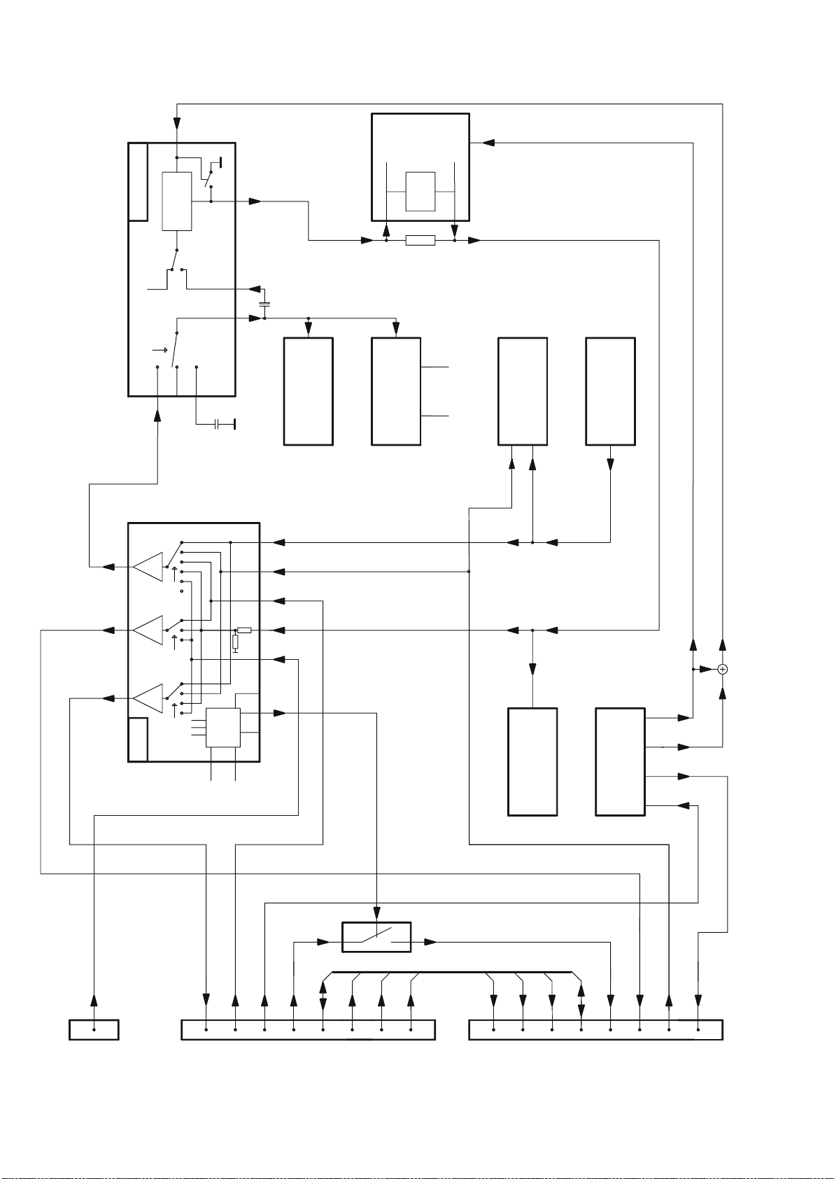
2-18
Simple Blockdiagram
FFP
26
SYCA Video-Part
Testpict.
Generator
PLAY
REC/EE
293132
VSB
VPO
VSB
7502
18
SDA5652
Secam
0E
VPO
Bypass
15
not for VPO
9
OFP
VOUT
VBS
VOUT1VOUT2
7004-B
LA71595M
IN3
IN2
IN1
VREC
15
7072
VS
34
36
38
LA7339A
VS_ SEC
VBS
VFVVIN1
21615
x1x2x2
Mute
10k
10k
2
IC
BUS
7904
STV6401
IO
11
SCL
2
9
SDA
I C-Bus
from AIO1
VIN2
VOUT
VFR
51210864
13
MON
7
VREC
17
7502
VS-SECAM
SDA5650
VPS/ PDC
54
SDA
2
I C-Bus
VPS/PDC
SCL
from AIO1
FOME
7530
VIN1
V
F
LM339D
FOME
VOUT
1
1701
MODULATOR
VFV
TUMOD
FV
FV
VFV
7899-B
CENTRAL CONTROL
AIO1
IO-Block diagram 2 Scart-Video-Mono&Stereo
not for OSD
36
FFP OFP
55 32
8SC18SC2
61
MON
7913
VFR
1954A
Front plug
Video from
Front plug
D
VOUT2
197201181516101016151911207
1952
Scart2
Video Out
VIN2
Video In
8SC2
Switching
blanking
Blanking
pin10
red
red
pin10
blue
green
green
blue
Scart1
1951
blue
blue
red
green
green
pin10
red
pin10
blanking
Blanking
VOUT1
Video Out
VIN1
Video In
8SC1
8
Switching
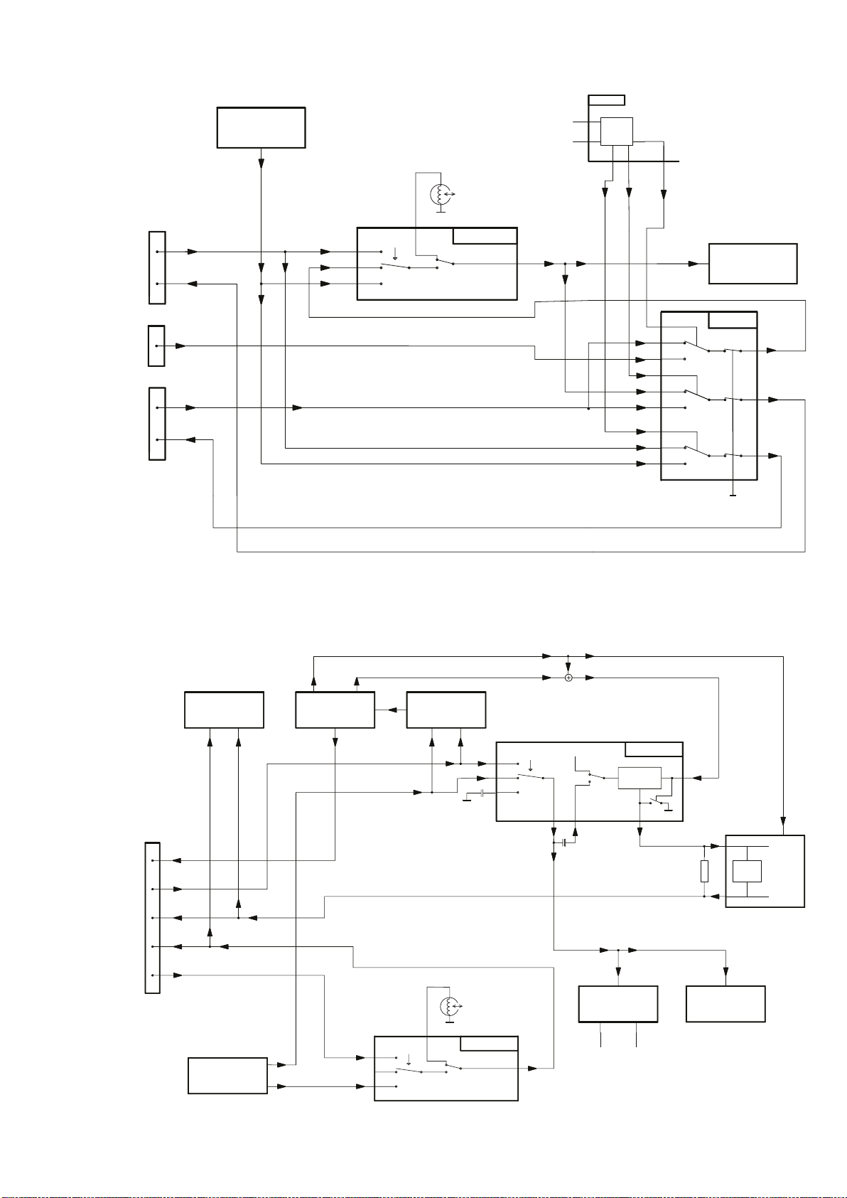
2-19
Audio In 1
Audio Out 1
Front plug
Audio In 2
Audio Out 2
Scart1
1951
Front plug
1954A
Scart2
1952
2+6
1/3
2+6
1/3
AINF
AIN1
AOUT1
AIN2
AOUT2
FV
FV
AFV
AIN1
AIN2 - AINF
AFV
STV6401
7904
11
SCL
SDA
PB-Head
IO
BUS
2
IC
9
7
5
13
IS1
MONDEC
AL
IN1
76
IN2
78
IN3
80
PLAY
REC/EE
SYCA Audio-Part
LA71595M
7004-A
AMLP
96
11
AIN2
12
AINF
13
MON
9
AMLP
5
AIN2
3
DEC
10
AIN1
2
AF1
1
AMLP
3
0
1
0
1
0
1
FV
MODULATOR
TUMOD
7911
6
IO
AIN2 - AINF
14
4
15
HEF4053
1701
AOUT1
AOUT2
Switching
Video In
Video Out
Audio Out l
Audio In l
Scart 1
1951
FV
MODULATOR
8SC1
8
VIN1
20
VOUT
19
AMLP
1/3
AIN1
2+6
FV
1701
TUMOD
31
AMLP
VOUT
FV
VFV
AFV
OFP
DE
FFP
36 32
DE
34
8SC1
AIN1
AFV
IO-Block diagram 2 Scart-Audio-Mono
7004-B
LA71595M
AMLP
96
not for OSD
VREC
VPS/PDC
SYCAVideo-Part
PLAY
REC/EE
Generator
VREC
17
Testpict.
293132
SDA5650
VPS/PDC
45
2
I C-Bus
SCL SDA
VSB
FFP
26
VSB
not for OSD
VOUT
VS_
SEC
VS-SECAM
VPO
18
Secam
0E
Bypass
15
VREC
15
LA7339A
9
SDA5652
OSD
70727502
OFP
7502
FOME
FOME
93
FOME
VFV
VIN1
VIN1
VFV
PB-Head
VS
IN1
38
IN2
36
IN3
34
AL
IN1
76
IN2
78
IN3
80
PLAY
REC/EE
SYCA Audio-Part
7004-A
LA71595M
QMB1 IO-Block diagram 1 Scart-Audio-Video-Mono
D

2-20
Simple Blockdiagram FM Audio / Linear Audio processing
Volume L/R
9
35
REC
+15dB
AH2
mute
-48dB
FM Audio
TapeDeck
1965-1 1965-3
11
EQ-AmpLine
REC
EtoE
APH
4
PB
AHC
36 10
Processing
Head
AH1
37
Amplifier
PB
21
7004-A
AL
78
AMLR
ARH
7
ALC Rec-Amp
22
0dB
+15dB
Level
mute
LA71595M
-
Mute
Linear-Aud.
96
Processing
mute
AMLP
TDA 9605H
FM-Audio Processing
LEFT
L+R
L+R x VolumeLR
Lin.Audio Sel
L x Volume
OutputSel
RIGHT
STEREO
NOR+ST
NORMAL
NOR+L
NOR+R
mute
InputSel
7650
AF
ST/NIC
7760/7761
TUNER
CINCH
4/5
2/3
AFL
AFR
L
R
Dec.
Stereo
MSP3415
TDA9873
SIF2
12
EXT1
8/9
6/7
Nicam
EXT2
EXT3
SAP
AINFL
AINFR
AIN1L
AIN1R
EXT2
LineSel
OutSel
16
AOUT1L
AOUT1R
EXT1
OutSel
TUNER
DecoderSel
201719
AIN2L
AIN2R
Mute
AFC
AOUT2L
mute
13
AMCO
AOUT2R
OutSel
STEREO
Env-Sel
L
R
44
TRIA/DC
57
Demod.
TDA 98xx
7721
FV
17
3
TUMOD
FV
1701
D
1954-B
L
AMCO
R
Front
CINCH
L
IO 1956
R
Rear
CINCH
IO
1951
TVC
7899-B
2
6
1
3
SCART1
IO
1952
2
6
1
3
SCART2
DECK-µC
DE
2-21
SERVICE MODES
1. Special functions
1.1 Erasing the EEPROM
- Disconnect from mains
- Push and hold down the Standby key, reconnect to mains
and keep the Standby key depressed for a further 3 sec.
All EEPROM data will then be erased and initialised (timer and
transmitter channels). The internal processor RAM will also be
erased, but the option codes, deck parameters and adjustment
values are maintained.
1.2 After changing the EEPROM or Motherboard
the following steps must be carried out:
Step 40: Option code input
Step 51: Gap position adjustment
Step 52: Studio Picture control adjustment
Step 53: Input of clock correction
Step 62: Adjustment of Audio Linear Playback Level
Step 99: Clock frequency output
2. Service test program
2.1 Introduction
The software program for the control, deck and operating
microprocessors includes a service test program. It was divided into
the following steps, with the following modes:
Step 00: Display of mask version number
Step 01: Check of the drive positions
Step 02: Display of the deck - error codes
Step 03: Deck - sensors and manual tracking
Step 04: Display of operating hours counter
Step 05: Display of the IIC-Bus Communication
Step 10: Operation without drive - dummy mode
Step 40: Option code input
Adjustment Steps in the service test program:
Step 51: Gap position adjustment
Step 52: ‘Studio Picture control‘ adjustment
Step 53: Input of clock correction
Step 62: Adjustment of Audio Linear Playback Level
Step 98: Display test
Step 99: Clock frequency output
In the service test program, all drive functions apart from the channel
search and channel change mode can be carried out. The program
position set before entering the service test program is maintained.
2.2 Activating the service test program
Press and hold down the STOP key on the remote control. Then
press the PLAY key on the recorder and keep it depressed for at
least 5 sec. The STOP key on the remote control may be released
whilst the PLAY key on the recorder is pressed.
The service test program can be selected in any operating mode
apart from the channel search, install, clock set-up and cassette
length calculation mode. The recorder and all drive functions are fully
operational in the service mode.
The display shows, for instance:
By pressing the SELECT key on the remote control, all step modes
may be left and the currently selected step number appears and
flashes.
Other service steps are selected with the UP and DOWN keys or the
numerical remote control keys. By pressing the SELECT key on the
remote control whilst the Step is flashing, the respective mode can
be entered or left.
If a step is selected to which no mode is assigned, the displays
shows - - and flashes.
To leave the service program, press the STAND-BY key or
disconnect recorder from mains.
2.3 Service mode functions
Endurance test
In the service test program, the recorder can be endurance tested.
For this purpose, use a cassette and activate PLAY or REC. The
functions are then repeated continuously. In RECORD, the recorder
does not move to EJECT at the tape end, but to REWIND, after which
it starts to RECORD again. This test serves to detect intermittent
faults. The last error is stored in the EEPROM. (The fault remains
stored even after a power failure).
The endurance test is ended by pressing STOP or leaving the service
test program.
PLAY TAPE END RECORD
TAPE BEGIN REWIND TAPE BEGIN
2.4 Description of steps with modes:
Step 00: Display of mask version number
After activating the service test program, step 00 and the mask
version number are automatically displayed.
Central control mask
The mode can be left again by pressing the SELECT key on the
remote control. The currently selected position number appears and
flashes on the display.
Central control mask
A step between 00 and 99 can now be selected
GB

2-22
Step 01: Checking the drive positions
By pressing the SELECT key whilst Step 01 is flashing, the drive
position appears on the display.
The FTA signal from the photoelectric barriers which controls the
revolutions of the loading motor is used to check the drive condition.
The drive position is shown as a 3-digit decimal number by counting
the FTA pulses on the display.
(e.g. 213 = Play)
Table of drive positions:
Status Position
(FTA dec)
Eject 007 +2/-2
Index 191 +0/-2
Stop 200 +4/-4
Play 213 +4/-4
Reverse 237 +2/-0
Function of the Init switch:
The diagram shows the function of the Init switch, depending on the
position of the deck. The number of FTA pulses is important for the
position of the drive.
A:DC,2V/Div,0.5s/Div
B:DC,2V/Div,0.5s/Div
Stopping of head drum motor
This is monitored with the PG/FG signal. The signal is discharged
from the e.m.f. of the non-conducting spools of the head cylinder
motor, showing the position of the head cylinder.
Capstan motor fault
This is monitored with the FGD signal.
If one of the above sensor signals is not available, the recorder tries
to put the lift into the EJECT position.
Explanation of deck error codes and deck error status
The last error code is stored and remains in the EEPROM, even if the
recorder is disconnected from the mains.
The error code can be erased by pushing the CLEAR button on the
remote control.
The display shows, for instance:
The left digit shows the error:
(e.g.: Error 2 = Capstan error)
Error table:
0
no error
1
threading error
2
no capstan pulses
3
tape broken
4
no pulses left reel
5
no pulses right reel
6
head motor error
A
B
Eject
Play
Init switch
FTA pulses
Index/
Cass down
wind-rewind
Reverse
Step 02: Display of the deck error codes
By pressing the SELECT key whilst Step 02 is flashing, the deck
error code is shown on the display.
Checking the drive function
Loading and unloading time
The signal (FTA) of the photoelectric barrier which controls the
revolutions of the loading motor is used as a reference for the loading
and unloading time.
The 3 digits on the right represent the deck error condition:
(e.g.: 053 = during Play )
Functiontable:
012
Standby 114 VISS write 211 Slowmotion 1/24
014 Autotracking 115 Viss erase 212 " " 1/14
031 Play-3 125 Tuner - Stopout 215 " " 1/7
034 Slow_reverse 126 Auto Remain Funct. 216 " " 1/2
041 Still Picture 130 ATTS Fun c tion 217 " " -1/24
042 Fast 168 Frame+ 218 " " -1/14
044 Play-9 169 Frame- 219 " " -1/7
045 Eject 170 Play-11 220 " " -1/2
046 Play9 171 Play-7 222 Edit Record
047 Play-1 172 Play-5 223 Align of Gap
048 Pause 173 Play5 238 Pause
050 Rewind 174 Play7 239 SPC align
052 Wind 175 Play11 246 Edit Pause
053 Play 196 Tuner - Eject 247 Slow motion 1/10
054 Stop out 197 Standby Eject 248 " " 1/18
055 Record 199 Audio Dubbing 249 " " -1/10
112 Index next 202 Audio Dubb. Pause 250 " " -1/18
113 Index previous 206 Reset Tapecounter 253 Key Released
Stopping of supply or take-up reels
The tacho signals of the left (WTL) and right (WTR) winding disks are
used as control reference.
GB
The error code can be reset in this step with the CLEAR key.
2-23
Step 03: Deck sensors and manual tracking
By pressing the SELECT key whilst step 03 is flashing, the deck
sensors will be displayed in one digit as either 1 or 0.
nl z A are used to display the deck status.
START init switch (INIT)
END record protection (RECP)
DEC Loading pulses (FTA)
In the service test program, the tracking is always in the centre
position.
Only in this step can the value for the required tape running setting be
changed, manually in the PLAY function with the UP / DOWN keys.
After leaving the mode with the SELECT key, the tracking value
always resets itself to the centre position and cannot be changed.
Step 04: Display of the operating hours counter:
By pressing the SELECT key whilst step 04 is flashing, the operating
hours counter shows how many hours the head disk has turned. The
hours are displayed as a 4-digit decimal number.
Step 10: Operation without drive - dummy mode
Before activating this mode with the SELECT key, the recorder
must be in the EJECT position.
Enter the mode by pressing the SELECT key . The motors are then
switched off and the sensors will be ignored by the deck
microprocessor. The drive can now be dismantled from the
motherboard (see dismantling instructions). Only install drive if
recorder is disconnected from mains. For signal tracking, the
recorder can be set to all drive conditions, i.e. signal electronics,
audio and IO processing are switched to the respective operating
mode.
nl z A are used to show the deck status
START init switch (INIT)
END record protection (RECP)
DEC loading pulses (FTA)
Step 40: Option code input
If a new EEPROM is installed in the course of repairs, it must be
initialised.
By pressing the SELECT key whilst step 40 is flashing, the decimal
option A appears in the display.
Step 05: Display of the IIC - Bus Communication:
By pressing the SELECT key whilst step 05 is flashing, the available
IIC- components will be displayed with symbols.
Symbol Description Component Position
VPS or VPO IC SDA5650 or SDA5652 7502
v
FM ST / NIC IC MSP 3415D 7761
DEC
FM St IC TDA 9873 7760
x
Video switch IC STV 6401 7904
W
FM Audio IC TDA 9605H 7650
D
Tuner Philips TP9xx 1701
k
o
Tuner Alps TMRxx/TCBZ4 1701
Modulator Phil TP9xx 1701
u
LP
Modulator Alps TMRxx/TCBZ4 1701
8
Signal electr. IC LA71595M 7004
The following errors are visible in the display when the start up
routine of the set isn’t working properly.
E000 IIC-Data line is low
E001 IIC-Clock line is low
E002 EEPROM give no acknowlegement
By entering a 3-digit decimal code, the correct features are set.
These codes are shown on the type-plate of the recorder.
After pressing the OK key on the remote control, the entered code is
saved. The display shows OK for approx. 3 sec. and then the stored
value in decimal format.
By pressing the UP and DOWN keys, the available options (A to G)
can be selected. The display shows the last stored value in decimal
format.
In case of an invalid entry (value >255) the activation of the OK key
causes the content of the last stored option to be displayed and OK
does not appear in the display.
Depending on the model, some bits are software or default protected
and cannot be changed by an entry. In this case, the display shows
OK, but the display returns to the default value.
Step 98: Display Test
By pressing the SELECT key whilst step 98 is flashing, all segments
of the display are illuminated.
The step is exited by pressing SELECT again.
GB


2-25
ADJUSTMENT INSTRUCTIONS
Test equipment:
1. Dual-trace oscilloscope
Voltage range : 0.001 ~ 50 V/div
Frequency : DC ~ 50 MHz
Probe : 10:1, 1:1
2. DVM (Digital voltmeter)
3. Frequency counter
4. Sinus generator
Sinus : 0 ~ 50 MHz
5. Test pattern generator
6. VHS Alignment Tape 4822 397 30103
SPC Alignment Tape 4822 397 30268
VHS-test cassette
1. Video signal processing (VS-SEC)
Service tasks after replacement of ICs 7004, 7072:
Before commencing adjustment:
1.1 3.3 MHz adjustment [3089] (for SECAM)
Purpose:
Consequences of incorrect settings:
Call the service test program and enter Step 10 (Dummy
mode). Remove the drive from the motherboard.
T o adjust the mixing oscillator
Cross patterns in coloured areas, coloured noise.
TP ADJ. MODE INPUT
IC7072
pin 17
R3089
Dummy mode
step 10
playback
1.2 MHz sinus
100mVpp,
wire 9021
(FMPV)
TAPE MEAS. EQ. SPEC.
Oscilloscope
Video pattern
generator
Sinus generator
adjust to
optimum
sinus
PB
Counter Reading Start 0 0040 ± 8 0310 ± 12
Video B lan k B &W Pattern Color Bars
Audio Blank 6k H z (mono) 40Hz, 3kHz, 15kHz (Mono & Stereo)
How to read the adjustment procedures:
VCR mode:
Example using:
SP SELF-RECORDING AND
PLAYBACK
SP-record video signal and
Connecting point
(Test Point) of
measuring
equipment
play back the recorded
tape section
Adjustment
component
Test signal
required for the
adjustment and
feed-in point
A: AC, 50mV/Div, 50ns/Div
IC 7072 Pin 17
1.2 SECAM chrominance record current
adjustment [3088]:
Purpose:
Symptom, if incorrectly set:
T o set the optimum record SECAM chroma level.
If the record level is too high, beats may appear on the
picture. If the level is too low, the colour may be degraded.
TP ADJ. MODE INPUT
CSRP
pos.9034
R3088
Dummy mode
Record
Preset E2
(VIDEO IN E2)
Red Picture SECAM
75% Saturation
TAPE MEAS. EQ. SPEC.
Blank
Tape
Oscilloscope
Video Pattern
Generator
A=240 ± 15 mV
0V
pp,
TP ADJ . MODE INPUT
Pin 2 of
Con.1911
(FMRV)
R3054
SP. PLAYBACK
TAPE MEAS. EQ. SPEC.
Frequency-
Counter
Measuring
equipment
Tape needed for
adjustment
Blank
T ape
3,800MHz
±10kHz
Adjustment
Specification
Notes: With varying frame amplitudes, the setting is made for the
greatest amplitude.
REC
A
A: AC, 50mV/Div, 20us/Div
GB

2-26
2. Front End (FV)
Service tasks after replacement of IC 7705, coil L5702 and TUMOD:
2.1 AFC Adjustment:
Purpose:
Symptom, if incorrectly set:
2.1.1 P AL - AFC adjustment [5702]:
2.1.2 SECAM band 1 - AFC adjustment [3730]:
(SECAM L / L' only)
Before commencing adjustment:
- Switch to a band 1 SECAM L’ preset.
- Is the system switch, in the menu ‘MANUAL SEARCHING’, not
- A fine-tuning will be done and the system will switch to the
Correct adjustment of demodulator AFC - circuit
Bad or disturbed TV channel reception.
TP ADJ. MODE INPUT
IC 7705
Pin 17
(AFC
TP9719)
L5702
E to E
38,9MHz 500mV
at Tuner 1701 Pin 17
(TP9713,ZF-out)
TAPE MEAS. EQ. SPEC.
DC Voltmeter
Frequ. Generator
possible, press the right cursor key of the remote in the
‘CHANNEL NUMBER’ line for a short moment.
‘AUTO’ function.
2,5V ±0,2V
TP ADJ. MODE INPUT
IC 7705
pin 17
(AFC
TP9719)
R3730
E to E,
SECAM L' tuned
on this preset
33,9MHz 500mV
at Tuner 1701, pin 17
(TP9713, ZF-out)
TAPE MEAS. EQ. SPEC.
DC Voltmeter
Sinus Generator
2,5V ±0,2V
pp
pp
2.3 Attenuating the 40.4 MHz [5704]:
(SECAM only)
Service tasks after replacement of coil 5704:
Purpose:
Symptom, if incorrectly set:
T o attenuate the band I carrier rests.
Bad picture quality when the filter attenuates the picture
carrier (38.9MHz).
TP ADJ. MODE INPUT
OFW
1704
Pin 1
L5704
E to E
40.4 MHz, 300mV
at Tuner 1701 Pin 17
(TP9713,ZF-out)
rms
TAPE MEAS. EQ. SPEC.
Oscilloscope,
Sinus Generator,
Counter
If the adjustment is correct the signal at pin 1 of SFW [1704] must be
smaller than the input signal amplitude by at least 5 dB.
adjust minimum
amplitude
3. Deck electronics (DE)
Service tasks after replacement of IC 7463:
3.1 Motor frequency - adjustment [2492]:
Purpose:
T o adjust the working frequency of the head motor driver .
Result of an incorrect adjustment:
Head motor doesn’t start correctly.
Before commencing adjustment:
- bring VCR in to EJECT state
- disconnect set from main power source
- remove cable 8004 from connector 1948
- connect test point DRUM [9417] with 5VS1 [9869] (wires
on component side)
- reconnect to main power source
TP ADJ. MODE INPUT
2.2 HF - AGC adjustment [3707]:
Service tasks after replacement of ICs 7705, or TUMOD:
Purpose:
Symptom, if incorrectly set:
Set amplifier control.
Picture jitter if input level is too low and picture distortion
if input level is too high.
TP ADJ. MODE INPUT
Tuner
1701
Pin 17
(TP9713,
ZF-out)
R3707
Set tuned to
channel 27
4,5mV(74dBµV)
on aerial input
PAL white picture,
audio IF on,
no modulation
TAPE MEAS. EQ. SPEC.
Oscilloscope
Video Pattern
Generator
GB
550mVpp +/-50mV
(use a 10:1 probe )
Connector
1948
Pin 1
C2492
EJECT
TAPE MEAS. EQ. SPEC.
Oscilloscope,
Counter
1e
1e2e
A: DC, 5V/DIV, 50ms/Div
Connector 1948 PIN1-3
2e
153.6 ms = 6e
>
153,6 ms ±1,5ms
see Diagram
0V

2-27
4. Servo System (AIO1)
Service tasks after replacement of the head drum or EEPROM.
4.1 Setting the gap position (GAP):
Purpose:
Symptom if incorrectly set:
After a correct adjustment, the display shows 1; 0 when incorrect.
To leave the step, press SELECT.
T o determine the correct head switching point
during playback.
Head switching fault and/or vertical picture flickers.
- Enter the service test program and, whilst step display is
flashing, enter the step number 51, using the numerical keys.
- Insert a test cassette (e.g. 4822 397 30103) with the standard
video signal in the VCR.
- By pressing the SELECT key whilst step 51 is flashing, the
automatic adjustment is triggered and stored in the EEPROM .
TP ADJ. MODE INPUT
Stop
Service Mode
TAPE MEAS. EQ. SPEC.
VHS Alignment
T ape
Call up Step 51 of
Service Mode
5. Audio linear - ( AL)
Service tasks after replacement of coil L5600, IC7004 or the audio
heads:
5.1 Adjusting the erasing frequency [5600]:
Purpose:
Symptom, if incorrectly set:
connector
5.3 Adjustment of bias current [3625]:
Purpose:
Symptom, if incorrectly set:
T o set the correct recording erasing frequency .
Erasing frequency or its harmonics cause audio faults.
TP ADJ. MODE INPUT
PAL white picture,
1965
pin 5
L5600
Record E1
with sound on E1
(1kHz or 10kHz)
TAPE MEAS. EQ. SPEC.
Blank
T ape
T o set the optimum record bias current.
If the audio level is too high, the higher frequencies of the
linear sound are too low.
If the level is too low, the higher frequencies are too
strong and sound distortions increase.
Frequency
Counter
70kHz
±10kHz
Causes of incorrect adjustment :
Incorrect standard video signal.
Scanner fault.
Microprocessor fault.
4.2 ”Studio Picture control” adjustment (SPC):
Purpose:
Symptom if incorrectly set:
Adjustment of the reference level for the SPC.
The picture is played back at a lower resolution than
would be possible.
TP ADJ. MODE INPUT
Stop
Service Mode
RF or A1- input,
black picture
without BURST
TAPE MEAS. EQ. SPEC.
SPC Alignment
T ape
- Video signal via Scart or aerial
- Enter the service test program and, whilst the step is flashing,
input the step number 52, using the numerical keys.
- Insert SPC Alignment Tape 4822 397 30268.
- By pressing the SELECT key whilst step 52 is flashing, the
recorder makes a recording in SP mode (approx. 10 sec.) and in
LP mode (approx. 10 sec.), rewinds and carries out a playback
with automatic adjustment.
- After a correct adjustment the display shows 1, and 0 for
incorrect adjustments.
Call up Step 52 of
Service Mode
TP ADJ. MODE INPUT
C2613
(TP BIAS)
R3625
Record E1
PAL white picture,
with sound on E1
(1kHz or 10kHz)
TAPE MEAS. EQ. SPEC.
Blank
T ape
Checking the 'bias' adjustment:
Apply a sine-wave signal with an amplitude of 50mVeff to the
SCART audio input. Record the 1kHz signal and 10kHz signal for 30
seconds each. Play back the recording and check that the amplitude
difference is in the ±3dB range. If this is not the case, correct the
value for the magnetic biasing current. If the treble is too low, the
bias current should be reduced slightly. If the distortion is too great,
the bias current should be increased slightly .
(approximate value: +1V = -1dB Treble).
AC Millivoltmeter,
Oszilloskop,
Video Pattern
Generator
14V
±1V
RMS
(70kHz)
RMS
To leave the step press SELECT.
GB

2-28
5.3 Adjustment of the audio linear playback
amplitude [IIC-bus]:
Purpose:
Symptom, if incorrectly set:
– Enter the service test program and, whilst step display is
T o set audio part amplification LA71595 [7004-A]
Playback sounds too low or too loud.
flashing, enter the step number 62, using the numerical keys.
TP ADJ. MODE INPUT
Pin 1 of
Scart 1
(Audout)
refer to
description
SP Self-recording
and Playback,
Service mode
call up Step 62
(Video white picture)
Audio in Scart 1,
700mV
RMS,
1kHz
TAPE MEAS. EQ. SPEC.
Blank
Tape
Video Pattern,
Frequency
Generator
By pressing the SELECT button whilst step 62 is flashing, the output
select is switched to Mono and the display shows, for instance:
– Make a recording of the audio signal on E1.
– Connect the millivoltmeter to Scart1 Pin1(Audio out) and play
the recording back.
– The level on Scart 1, Pin1 (Audio out) can be adjusted to the set
value by pressing the UP (value increases) or DOWN keys
(value decreases).
(The amplitude changes by 1 dB each time the key is pressed).
The range is shown in the display by the numbers 0...31.
– The value is automatically stored in the EE-PROM
each time the button is pressed.
AC Millivoltmeter,
500mV
±50mV
RMS
Determining the deviation (in ppm):
f
..... measured frequency
mess
f
........target frequency (8192,00 Hz)
nom
Deviation = 1x10⁶ x (f
mess
- f
nom
) / f
nom
Determining the correction value for Step 53:
Correction value = Deviation / 0.763 + 128 (round off to whole
number)
The calculated correction value must be between 0 and 255
(change quartz otherwise), and must be entered in Step 53 and
saved.
This step can either be exited by performing a main power source
reset, after which the service program must be entered again or by
pressing any key on the set, before step 53 can be entered.
Example:
f
=8191.97Hz f
mess
=8192.00Hz
nom
Deviation = 1x106 x (8191.97 - 8192.00) / 8192.00 = -3.662
Correction value = -3.662 / 0.763 + 128 = 123.20 = 123
6.2 Inputting the clock correction
Before carrying out step 53, the correction value must be
established in step 99.
By pressing the SELECT key whilst step 53 is flashing, the display
shows, for instance (128 is the default value of an empty EEPROM):
6. Display Control (AIO2)
Service tasks after replacement of the clock quartz [1170] or the
EEPROM:
6.1 Clock frequency output
Purpose:
Symptom, if incorrectly set:
Remove the Motherboard from the frame and bring it into the service
position.
Enter the service test program and, whilst step display is flashing,
enter the step number 99, using the numerical keys.
After entering with SELECT, the display is switched off and the
watch symbol is flashing, no further function can be carried out. At
the CLOCK ADJUST measuring point [7899-A, pin 71], the
uncorrected clock frequency of approx. 8192 Hz is always output.
Measure the output frequency with the calibrated counter (minimum
resolution of 6 digits) and note down the value (f
Setting the exact clock function.
The clock is too fast or too slow.
TP ADJ. MODE INPUT
7899-A
pin 71
CLOCK ADJ.
Stop
Service Mode
call up Step 99
TAPE MEAS. EQ. SPEC.
Frequency counter
with 6 digits
refer to description
below
).
mess
Using the numerical keys of the remote control, the established
correction value from Step 99 is entered as a 3-digit number (value
must be between 0 and 255).
After pressing the OK key on the remote control, the entered code is
stored, the display shows OK for approx. 3 seconds and then the
stored value in decimal format.
In case of an invalid entry (value >255), the activation of the OK key
causes the content of the last stored value to be displayed and OK
does not appear in the display.
To leave the step press Select.
GB

Adjustment table of the clock frequency:
Measured frequency in Hertz:
2-29
measured
clock
frequency
pos. 7899-A
pin 71
[Hz]
8192,00
8191,98
8191,96
8191,94
8191,92
8191,90
8191,88
8191,86
8191,84
8191,82
8191,80
8191,78
8191,76
8191,74
8191,72
8191,70
8191,68
8191,66
8191,64
8191,62
8191,60
8191,58
8191,56
8191,54
8191,52
8191,50
8191,48
8191,46
8191,44
8191,42
8191,40
8191,38
8191,36
8191,34
8191,32
8191,30
8191,28
8191,26
8191,24
8191,22
8191,20
corrected
value
for Step 53
input
128
125
122
118
115
112
109
106
102
99
96
93
90
86
83
80
77
74
70
67
64
61
58
54
51
48
45
42
38
35
32
29
26
22
19
16
13
10
6
3
0
measured
Time
deviation
minutes /
year
0,0
-1,2
-2,4
-3,7
-4,9
-6,1
-7,3
-8,5
-9,8
-11,0
-12,2
-13,4
-14,6
-15,9
-17,1
-18,3
-19,5
clock
frequency
pos. 7899-A
pin 71
[Hz]
8192,00
8192,02
8192,04
8192,06
8192,08
8192,10
8192,12
8192,14
8192,16
8192,18
8192,20
8192,22
8192,24
8192,26
8192,28
8192,30
8192,32
corrected
value
for Step 53
input
128
131
134
138
141
144
147
150
154
157
160
163
166
170
173
176
179
deviation
minutes /
-20,8 8192,34 182 20,8
-22,0 8192,36 186 22,0
-23,2 8192,38 189 23,2
-24,4 8192,40 192 24,4
-25,6
-26,9
-28,1
-29,3
-30,5
-31,7
-33,0
-34,2
-35,4
-36,6
-37,8
-39,1
-40,3
-41,5
-42,7
-43,9
-45,2
-46,4
8192,42
8192,44
8192,46
8192,48
8192,50
8192,52
8192,54
8192,56
8192,58
8192,60
8192,62
8192,64
8192,66
8192,68
8192,70
8192,72
8192,74
8192,76
-47,6 8192,78
195
198
202
205
208
211
214
218
221
224
227
230
234
237
240
243
246
250
253
-48,8
Time
year
0,0
1,2
2,4
3,7
4,9
6,1
7,3
8,5
9,8
11,0
12,2
13,4
14,6
15,9
17,1
18,3
19,5
25,6
26,9
28,1
29,3
30,5
31,7
33,0
34,2
35,4
36,6
37,8
39,1
40,3
41,5
42,7
43,9
45,2
46,4
47,6
GB

1-8
Modifications
Description du système de publication des
modifications et des compléments à la
documentation technique.
Toutes les modifications et les compléments à la documentation
technique sont donnés dans les Infos Service.
Chaque info est repérée comme suit:
Exemple
VR 00 - 01 F
Langue
Numéro de séquence
Année
Magnétoscope
Une Info Service se compose d'une page de garde et dans certains
cas de feuilles de complément et/ou de remplacement.
Les feuilles de remplacement vienne remplacer les feuilles
existantes dans la documentation technique. Elles sont
reconnaissables grâce à une lettre, à la suite du numéro de la page,
incrémentée alphabétiquement.
Par exemple, la page 5-1a doit remplacer la page 5-1 dans la
documentation technique.
Les feuilles de complément sont à ajouter aux feuilles déjà
existantes dans la documentation. Elles sont reconnaissables grâce
à un chiffre, à la suite du numéro de la page, incrémenté
numériquement.
Par exemple, la page 5-1-1 vient à la suite de la page 5-1 dans la
documentation technique.
Sur la mécanique
12345678 009271 AT-P2/0 00151 10WD51
Code de production
Centre de production
Semaine de production
Type de mécanique
Code usine
Numéro de série
Remarque:
Le code de production et le N° de série sur la mécanique ne
correspondent pas nécessairement au code de production et au N°
de série sur l'étiquette à l'arrière de l'appareil.
Sur les platines
Les étiquettes sont généralement collées sur le côté cuivre de la
platine.
AVR 01102
12345 KW 015 WD 01 123456
Numéro de série
Code de production
Semaine de production
Nom de la platine
Code usine
Remarque:
Description du système de notification des
modifications dans l'appareil
T outes les éléments importants de l'appareil tels que: la mécanique,
les platines ou les modules, sont dotés d'une étiquette adhésive. Ces
étiquettes contiennent un certain nombre d'informations inhérentes à
la production.
La signification de ces informations vous est donnée ci-après.
Sur l'appareil
L'arrière de l'appareil comporte une étiquette de type comme ceci:
.FOR BY GEMSTARDEVELOPMENT CORP.
P
D
D
R
E
IE
.GEMSTARDEVELOPMENT CORP.
O
MADE IN EUROPEMADE IN EUROPE
220-240 V ~220-240V ~
AAA BBB CCC DDD EEE FFF GGG
AA
S
MODEL NO:MODEL NO:
PROD.NO:PROD.NO:
VN 37 0015 123456VN 37 123456
50Hz50Hz
VR110/02
Remarque:
- Lorsqu'un changement important intervient sur l'appareil, le code
de production est incrémenté d'un chiffre; par exemple
37 devient 38.
R
P
L
C
U
P
R
T
T
P
O
C
N
A
C
A
E
M
T
K
F
M
Service
O
N
R
U
P
R
E
A
N
F
O
A
M
M
L
Code d'options (A-G)
E
P
E
E
S
O
D
V
N
L
IS M
A
E
E
E
Code d'évolution
R
D
M
V
IC
E
E
R
L
T
AT
D
A
R
S
T
E
R
Y
S
IS
Modèle
D
A
S
M
T
W
N
E
S
W
UNDER LICENSE FROM
U
IE
M
G
IE
V
E
Y
V
W
G
B
W
O
O
R
H
H
S
SHOWVIEW IS A TRADEMARK APPLIED
O
S
SHOWVIEW SYSTEM IS MANUFACTURED
F
Numéro de série
Date de production
Centre de production (VN),
Code de production
Le code de production n'est pas toujours indiqué. Lorsqu'un
changement important intervient sur la platine, le dernier digit du
code usine est incrémenté; par exemple 6635.1 devient 6635.2.
- Lorsqu'un changement important intervient sur l'appareil, le code
d'évolution est incrémenté d'un chiffre; par exemple
AA devient AB.
F

2-1
AIDE AU DIAGNOSTIC
Remplacement des CMS (Composants
Montés en Surface)
Nous vous recommandons de procéder comme suit pour
remplacer les CMS utilisés dans cet appareil:
1. Travaux préparatoires
a. Fer à souder
Utilisez un fer à souder de type crayon de moins de 30W.
b. Type de soudure
Utilisez une soudure Eutectique
(63% d'étain, 37% de plomb)
c. Temps de soudure
4 secondes maximum.
Remarques:
a. Un CMS démonté ne doit plus être réutilisé.
b. Evitez les pressions trop fortes et les frictions sur les
électrodes des CMS.
2. Démontage des CMS
Saisissez le composant à l'aide d'une pincette et chauffez en
alternance ses deux connexions. Dès que la soudure a fondue sur
ses deux connexions, retirez le CMS en effectuant un mouvement
de rotation avec la pincette.
3. Montage des CMS
a. Etamez les pastilles sur le circuit imprimé.
Etamage
Fer à souder
Fig. 2-2
b. A l'aide d'une pincette, poussez sur le composant en soudant
ses deux connexions comme indiqué dans la figure ci-dessous.
Pincette
Fer à souder
Soudure
Fig. 2-3
Remarque:
Ne pas coller les CMS de remplacement.
Remarques:
a. Ne tentez pas de retirer le CMS avant de l'avoir désolidarisé de
la platine par un mouvement rotatif.
b. Veillez à ne pas endommager les pistes du circuit imprimé.
Pincette
CMS
Fer à souder
Fig. 2-1
Montage/démontage des circuit intégrés
FLATPACK
1. Démontage d'un circuit intégré Flat Pack
• Avec un fer à air chaud adapté
EXEMPLE
Fig. 2-4
F

2-2
a. Equipez le fer à air chaud pour le démontage de circuits FLA T
PACK. Chauffez le circuit à dessouder pendant environ 5 à 8
secondes.
b. En cours de chauffage, retirez le circuit intégré à l'aide d'une
pincette.
ATTENTION:
Ne chauffez pas les CMS proches du circuit intégré à dessouder
pendant trop longtemps; ceci risquerait de les endommager.
Circuit
Imprimé
Ruban
adhésif
Pincette
Circuit Intégré "FLAT PACK"
Fig. 2-5
Pour protéger les éléments voisins, collez un ruban isolant autour
du circuit intégré FLAT PACK.
Les circuit intégrés FLAT PACK sont collés sur le circuit imprimé.
Lors de leur retrait, veillez à ne pas endommager de pistes sous le
circuit ou a proximité de chaque pastille.
Fer à air chaud
adapté
b. Relevez les broches une à une, à l'aide d'une aiguille ou d'un fil
métallique, tout en chauffant les broches avec un fer à souder muni
d'une pointe fine ou à l'aide d'un fer à air chaud.
Aiguille
Fer à souder
Fig. 2-7
• Avec du fil de fer
a. Utilisez de la tresse à dessouder pour éliminer la soudure de
toutes les broches du circuit. Cette opération peut être simplifiée
en appliquant du flux décapant sur toutes les broches.
b. Fixez le fil de fer au plan de travail ou à un point d'ancrage
solide (voir fig. 2-8).
c. Tirez le fil de fer vers le haut dès que la soudure est fondue afin
de désolidariser la broche du circuit intégré du contact sur la
platine, tout en continuant à chauffer les broches suivantes à l'aide
d'un fer à souder ou d'un fer à air chaud.
• Avec un fer à souder
a. Utilisez de la tresse à dessouder pour éliminer la soudure de
toutes les broches du circuit. Cette opération peut être simplifiée
en appliquant du flux décapant sur toutes les broches.
Circuit intégré
"FLAT P ACK"
Tresse à
dessouder
Fer à souder
Fig. 2-6
Fer à air
chaud ..
Soulever en
douceur
Fig. 2-8
Remarque:
Si vous utilisez un fer à souder, vérifiez que le circuit intégré n'est
pas collé sur la platine, sans quoi vous risqueriez d'endommager le
circuit imprimé. Dans le cas contraire, chauffez le circuit intégré à
l'aide d'un fer à air chaud pour faire fondre la colle.
Point
d'ancrage
Fil de fer
.. ou fer à souder
F

2-3
2. Montage des circuits intégrés FLAT PACK
a. Utilisez de la tresse à déssouder pour éliminer tous les résidus
de soudures sur les pastilles du circuit imprimé, afin de faciliter le
montage du nouveau circuit FLAT PACK.
b. Le repère "•" sur le boîtier du circuit indique la broche 1. Ce
repère doit coïncider avec le 1 sur le circuit imprimé. Soudez les
quatre coins du circuit intégré (voir Fig. 2-9).
EXEMPLE
La broche 1 des circuit intégrés "FLAT PACK" est repérée par
un "•".
Fig. 2-9
Pré-soudage
Fer à souder
Mesure des tensions
Mire de barre couleur en mode ENREG. et LECTURE en vitesse
normale
Remarque:
Les tensions, en ENREG. et en LECTURE, sont indiquées dans
les schémas conformément à la figure ci-dessous.
Mode ENR. et LECT.
(Tension identique dans
les 2 modes).
Mode LECT.
Mode ENR.
Fig. 2-11
Oscillogrammes
Circuit
imprimé
c. Soudez toutes les broches du circuit intégré. Veillez à éviter
tout court-circuit entre les broches.
Circuit Intégré
"FLAT P ACK"
Fig. 2-10
Remarque
Tous les circuits intégrés ainsi que beaucoup d'autre semiconducteurs sont sensibles aux décharges électrostatiques et
doivent donc être manipulés conformément aux prescriptions
décrites au chapitre AVERTISSEMENTS.
1 Point de connexion
2 Amplitude
3 Base de temps
4 Mode de fonctionnement
2
1
4
3
Fig. 2-12
Indication des tensions des diodes zéner
La tension zéner des diodes zéner est indiquée comme telle dans
les schémas.
Exemple:
BZX79C20............Tension zéner: 20 Volts
F

2-4
Identification des connecteurs dans les
schémas
Chaque connecteur est noté avec un numéro de connecteur et un
numéro de broche indiquant à quoi il est relié, ou autrement dit sa
contre-partie.
Utilisez le schéma d'interconnexion pour retrouver les liaisons
entre les différents connecteurs.
Exemple:
Les connexions entre les platines sont notées comme ci-dessous.
Numéro du connecteur
et numéro des broches
sur la platine
Platine sur laquelle
ce connecteur est
raccordé
Information sur les Points T est
Sur ce modèle, les Points Test ou les liaisons des composants
servent de points de contact pour les réglages et les contrôles.
Pour tout point de mesure autre que les Points Test ou les liaisons
accessibles des composants, utilisez les pistes du circuit imprimé.
Retrait ou mise en place des câbles plats
a. Retrait
Retirez le câble avec précaution en prenant garde à ne pas
endommager les différents fils (voir fig. 2-14).
Cable plat
TIRER
Connecteur
Broche 1
Circuit Imprimé
Fig. 2-13
Numéro du connecteur
sur lequel le connecteur
de gauche se raccorde
1
Fig. 2-14
b. Mise en place
1. Placer le câble plat de telle sorte que les lignes sur le câble
coïncident avec les broches du connecteur (voir fig. 2-14).
2. Introduisez les fils du câble plat dans le connecteur en veillant
à ce que les différents fils et trous correspon- dent bien.
REMARQUE: Après la mise en place, vérifiez le raccordement
et assurez-vous qu'aucun fil n'est tordu ou en contact avec un
autre.
F

Instructions de démontage
2-5
Instructions générales pour le démontage
d’éléments du boîtier, de composants
électroniques et de la mécanique
Avant tous travaux de démontage ou de remontage
sur l’appareil, commencez par débrancher la prise
secteur.
Du fait de la présence de tensions secteur côté
primaire de l’alimentation à découpage (Hot Part), il
est indispensable d’utiliser un transformateur
d’isolement pour cet appareil.
Pour retirer la mécanique ou l’ensemble mécanique platine principale, ne pas les saisir par les traverses
du porte-cassette !
Les composants insérés sous la mécanique doivent
être positionnés précisement !
Pour la recherche de pannes au niveau de l’alimentation,
il est recommandé d’utiliser un transformateur d’isolement
réglable.
Toutes les vis du magnétoscope peuvent être desserrées
ou serrées au moyen d’un tournevis Torx 10
1 .
1. Couvercle (fig. 1)
- Dévisser les quatre vis (A).
- Pousser le crochet de maintien (S) vers l’intérieur et soulever
simultanément le couvercle pour le dégager de la rainure.
- Pousser le couvercle du boîtier d’environ 1 cm en arrière.
- Pousser les parois latérales du couvercle vers l’extérieur
d’environ 1 cm (au milieu en bas), puis retirer le couvercle vers
le haut.
A
ä
Fig. 1
S
ä
S
ä
A
ä
A
A
S
S
S
Remontage
Pour le remontage, procéder dans l’ordre inverse.
2. Fond (fig. 2)
Le fond ne doit pas être retirée du cadre !
3. Panneau avant (fig. 2)
Travaux préparatoires
Démonter le couvercle du boîtier comme décrit au point 1.
- Placer l’appareil de telle sorte que le fond soit tournée vers le
haut.
- Déverrouiller dans l’ordre, de gauche à droite ou de droite à
gauche, les six crochets de maintien (S).
- Retirer le panneau vers l’avant.
- Pour les appareils dotés d’une platine Shuttle ou d’une platine
connecteurs, déconnecter le cable de liaison avec la platine
principale.
Remontage
Pour le remontage, procéder dans l’ordre inverse (appareil en
position de fonctionnement).
Important
- Le levier du volet cassette doit être introduit dans le guidage
du volet.
- Contrôler si tous les crochets de maintien sont bien
enclenchés.
Fig. 2
ä
ä
ä
S
ä
S
1
en vente dans les commerces spécialisés
F

2-6
4. Démontage de l’ensemble platine principale mécanique (fig. 3) (fig. 4)
Travaux préparatoires
Démonter le couvercle comme décrit au point 1.
Retirer le panneau avant comme décrit au point 3.
- Mettre l’appareil en position de fonctionnement (fig. 3).
- Desserrer les deux vis (B) de la traverse et retirer cette
dernière vers le haut.
- Pousser le porte-cassette en arrière de 5 cm après avoir
débloqué les deux verrouillages.
- Desserrer et retirer les quatre vis de fixation (C).
- Déconnecter le câble de prises cinch (K) et le câble de masse
(M) de la platine connecteurs (le cas échéant).
- Dégager les câbles (K1; K2; K3) de leurs guidages au dos du
cadre.
- Dégager le porte-prises cinch avec les prises et la platine du
cadre vers le haut (le cas échéant).
- Placer l’appareil de telle sorte que le fond soit tournée vers le
haut.
- Déverrouiller les 8crochets de maintien (S) : côté droit en
premieren partant de l’arrière vers l’avant, puis ceux du côté
gauche en allant aussi de l’arrière vers l’avant.
- Une fois que l’ensemble platine principale - mécanique s’est
dégagé du cadre par l’effet de son propre poids, déverrouiller
unedeuxième fois le crochet de maintien (S) près de la prise
secteur.
- Le cadre peut être retiré vers le haut.
- Retourner l’ensemble platine principale - mécanique et, si
nécessaire, l’amener en position de maintenance (fig. 5).
L’appareil peut fonctionner dans cette position mais la fonction
”Eject” ne doit PAS être activée !!!
M/K
ä
B
ä
K1
C K2 K3
ä
ä
C
ä
ä
C C B
Lift protection
ä
ä
ä
Attention:
Ne pas effectuer de réglages lorsque l’appareil est en position
de maintenance.
Ne PAS activer la fonction ”Eject” !!!
Montage
- Placer le cadre sur une surface plane, ouverture vers le haut.
- Saisir latéralement la mécanique au niveau du porte-cassette,
placer l’ensemble platine principale - mécanique dans le cadre
et appuyer doucement, en veillant à ce que la prise
d’alimentation et la prise Péritel soient bien dans leurs
guidages.
- Vérifier que les 8 crochets de maintien (S) sont tous bien
enclenchés.
- Fixer la mécanique au moyen des quatre vis de fixation (C).
- Amener le porte-cassette en position ”Eject”.
- Mettre la traverse en place sur le cadre, côté biseauté vers
l’arrière, et la fixer au moyen des deux vis (B).
- Introduire les prises cinch dans le guidage et les enclencher.
- Connecter le câble cinch et le câble de masse (K ; M) (le cas
échéant).
- Placer les câbles (K1; K2; K3) dans les logements prévus à
cet effet dans le cadre.
- Mettre en place le panneau avant et le couvercle du boîtier.
Fig. 3
ä
ä
ä
ä
SS
ä
ä
Fig. 4
F
ä

5.Démontage de la mécanique
(fig. 3)(fig. 5)(fig. 6)
Travaux préparatoires
Démonter le couvercle du boîtier comme décrit au point 1.
Retirer le panneau avant comme décrit au point 3.
- Desserrer les deux vis (B) de la traverse et retirer cette
dernière vers le haut.
- Après avoir débloqué les deux verrouillages du porte-cassette,
pousser ce dernier de 5 cm en arrière.
- Desserrer et retirer les quatre vis de fixation (C) de la
mécanique.
- Desserrer et retirer la vis de masse (D) au dos (introduire le
tournevis par l’orifice de la paroi arrière).
- Déconnecter les câbles de la mécanique.
- Fléchir la tôle de blindage du câble du tambour de têtes vers
l’arrière.
- Déconnecter le câble du tambour de têtes du connecteur.
- Ramener le porte-cassette en position ”Eject”.
- Relever légèrement la mécanique à l’arrière du côté gauche
pour déconnecter la liaison au moteur cabestan.
- Avec une pince à bec, débloquer les deux crochets de maintien
(S) et relever la mécanique au niveau des crochets.
- On peut ensuite dégager la mécanique de la platine principale.
Montage
Pour le montage, procéder dans l’ordre inverse.
C
Fig. 6
ä
ä
C
2-7
D
C
S
ä
C
S
Important
Veillez à ce que les câbles (K1; K2; K3) soient bien placés
dans leurs logements au dos du cadre, et que la vis de
masse (D) soit bien vissée !
D
ä
Fig. 5
Service position
F

2-8
Descriptions des circuits
1. Alimentation à découpage PS (partie PS) ...................................................................................................................................................9
1.1 Caractéristiques techniques : .........................................................................................................................................................................9
1.2 Principe dede fonctionnement........................................................................................................................................................................9
1.3 Entrée d’alimentation......................................................................................................................................................................................9
1.4 Phase de démarrage ......................................................................................................................................................................................9
1.5 Fonctionnement nominal ................................................................................................................................................................................9
1.6 Surcharge, limitation de puissance, burst mode ..........................................................................................................................................10
1.7 Mode veille ...................................................................................................................................................................................................10
2. Unité de commande DC (partie DC) ...........................................................................................................................................................10
2.1 Analyse de la matrice du clavier ...................................................................................................................................................................10
2.2 Récepteur infrarouge et analyse des signaux..............................................................................................................................................10
2.3 Commande et fonction de l’affichage VFD ..................................................................................................................................................10
3. Unité centrale de contrôle AIO (partie AIO) ................................................................................................................................................... 11
3.1 Interface analogique vers le µC ................................................................................................................................................................... 11
3.2 Commande de la LED fin de bande .............................................................................................................................................................11
3.3 Détection CMT (détection du signal vidéo avec CSYNC)............................................................................................................................ 11
3.4 EE-PROM ..................................................................................................................................................................................................... 11
3.5 Easy Link (P50) ............................................................................................................................................................................................ 11
3.6 Shuttle........................................................................................................................................................................................................... 11
3.7 Satmouse...................................................................................................................................................................................................... 11
4. Electronique de platine DE (partie DE) ......................................................................................................................................................11
4.1 Etage CTL ....................................................................................................................................................................................................11
4.2 Générateur Power On Reset (POR) ............................................................................................................................................................12
4.3 L’interface capteur ........................................................................................................................................................................................12
4.4 Interface vers le circuit de commande du moteur tambour .........................................................................................................................12
4.5 Interface vers le circuit d’attaque du moteur de chargement ......................................................................................................................12
4.6 Interface vers le moteur cabestan................................................................................................................................................................12
5. Frontend FV (partie FV) ...............................................................................................................................................................................13
5.1 LA HF/FI se compose des modules suivants :.............................................................................................................................................13
5.2 La HF/FI a été conçue pour la réception des systèmes suivants :..............................................................................................................13
5.3 Tuner et modulateur (TUMOD) ....................................................................................................................................................................13
5.4 Sélection FI...................................................................................................................................................................................................13
5.5 Démodulateur FI........................................................................................................................................................................................... 13
5.6 Démodulateur son ........................................................................................................................................................................................13
6. Traitement du signal vidéo VS (partie VS).................................................................................................................................................13
6.1 Fonctions de commutation du circuit de traitement LA71595M [7004-B] : .................................................................................................13
6.2 Enregistrement .............................................................................................................................................................................................14
6.2.1 Luminance .................................................................................................................................................................................................14
6.2.2 Chrominance PAL......................................................................................................................................................................................14
6.2.3 MESECAM ................................................................................................................................................................................................14
6.2.4 SECAM L ...................................................................................................................................................................................................14
6.2.5 Signal FM ..................................................................................................................................................................................................14
6.3. Lecture......................................................................................................................................................................................................... 15
6.3.1 Signal FM ..................................................................................................................................................................................................15
6.3.2 Luminance .................................................................................................................................................................................................15
6.3.3 Chroma PAL ..............................................................................................................................................................................................15
6.3.4 Chroma MESECAM...................................................................................................................................................................................15
6.3.5 Chroma SECAM L .....................................................................................................................................................................................15
6.3.6 NTSC .........................................................................................................................................................................................................15
6.3.7 PAL M,N.....................................................................................................................................................................................................15
6.4 Généralités ...................................................................................................................................................................................................15
7. Audio linéaire (partie AL).............................................................................................................................................................................16
7.1 Entrée/sortie audio pour appareils à 1 Péritel..............................................................................................................................................16
7.2 Entrée/sortie audio pour appareils à 2 Péritel..............................................................................................................................................16
7.3 Enregistrement audio linéaire ......................................................................................................................................................................16
7.4 Lecture audio linéaire ...................................................................................................................................................................................16
7.5 Mute audio linéaire .......................................................................................................................................................................................16
8. Audio HiFi pour appareils stéréo (partie AF) ............................................................................................................................................16
8.1 Généralités ...................................................................................................................................................................................................16
8.2 Entrée/sortie audio .......................................................................................................................................................................................16
8.3 Enregistrement audio HiFi............................................................................................................................................................................ 16
8.4 Lecture audio HiFi ........................................................................................................................................................................................16
8.5 Interface vers la partie Audio linéaire...........................................................................................................................................................16
9. Entrée/sortie IN/OUT (partie IO) ..................................................................................................................................................................16
9.1 Vidéo.............................................................................................................................................................................................................16
9.1.1 Audio pour appareils à 2 Péritel : ..............................................................................................................................................................16
9.2 Fonctionnement avec décodeur: (enregistrement ou arrêt) ........................................................................................................................16
9.2.1 Décodage d’un système crypté en provenance de la HF/FI.....................................................................................................................16
9.2.2 Entrée externe avec décodeur ..................................................................................................................................................................16
10. Follow Me (partie FOME) ...........................................................................................................................................................................17
11. VPS/PDC-, On Screen Display (partie VPO).............................................................................................................................................17
11.1 VPS/PDC ....................................................................................................................................................................................................17
11.2 Partie OSD..................................................................................................................................................................................................17
F

2-9
1. Alimentation à découpage PS
(partie PS)
1.1 Caractéristiques techniques :
Tension secteur : 195-264 V
Puissance max. : 15W / 40W (puissance permanente/de
Fréquence de découpage :40 kHz
rendement : env. 75 % à charge max.
Six tensions continues sont disponibles aux sorties du bloc
d’alimentation.
1.2 Principe de fonctionnement
Ce bloc d’alimentation travaille selon le principe de l’oscillateur
bloqué. A l’entrée du bloc d’alimentation [1300 à 2318], la tension
secteur est redressée et filtrée par le condensateur [2318]. Durant
la phase de conduction du transistor découpeur [7302], l’énergie
de cette tension redressée [2318] est transférée vers le
transformateur [5301, broches 1-3] où elle est accumulée sous
forme d’énergie magnétique. Durant la phase de blocage du
transistor découpeur [7302], cette énergie est transférée aux
sorties secondaires du bloc d’alimentation. Par le contrôle du
temps de conduction du transistor découpeur [7302], l’énergie
transférée à chaque cycle est régulée de telle sorte que les
tensions de sortie soient indépendantes des variations de la
charge ou de la tension d’entrée. Le transistor découpeur est
commandé par le circuit intégré [7303] fig.1.
1.3 Entrée d’alimentation
L’entrée d’alimentation va de la prise secteur [1300] au
condensateur [2318]. La tension secteur alternative est redressée
par les diodes [6310, 6311, 6312 et 6313], puis filtrée par le
condensateur [2318]. La bobine de réactance à courant de réseau
[5305] et le condensateur [2316] forment un filtre qui empêche que
des perturbations de l’alimentation ne se répercutent sur le
secteur. [1302], [3326] et [3323] protègent le bloc d’alimentation de
surtensions de courte durée pouvant apparaître sur le secteur, par
exemple par l’action indirecte d’un coup de foudre.
rms
pointe)
1.4 Phase de démarrage
Après le branchement sur le secteur, le CI [7303] charge le
condensateur [2310] en broches 6 et 8 par l’intermédiaire de la
résistance de démarrage [3318] et d’une source de courant.
Lorsque la tension du [2310] et par conséquent la tension
d’alimentation Vcc du CI [7303] atteint env. 13 V, le CI démarre en
envoyant des impulsions en broche 5 de sa sortie. Ces impulsions
commandent la porte du transistor à découpage [7302] (voir fig.2).
La fréquence à l’intérieur du CI est fixe (env. 40 kHz). La
consommation de courant du CI est normalement d’env. 5 mA.
Si Vcc tombe au-dessous d’env. 10V (p. ex. en cas de limitation de
puissance) ou si Vcc augmente jusqu’à env . 15V (interruption de la
boucle de régulation), la sortie du CI [7303, broche 5] est
désactivée. Toutes les tensions de sortie du bloc d’alimentation et
par conséquent Vcc baissent. Lorsque Vcc tombe au-dessous d’env.
6,5V, un nouveau cycle de démarrage commence (voir également
«Surcharge, limitation de puissance, burst-mode»)
1.5 Fonctionnement nominal
Dans le mode de fonctionnement nominal du bloc d’alimentation,
les processus périodiques à l’intérieur du circuit se décomposent
essentiellement en phases de conduction et phases de blocage du
transistor découpeur [7302]. Durant la phase de conduction du
transistor découpeur [7302], le courant circule de la tension
secteur redressée du condensateur [2318] à travers l’enroulement
primaire du transformateur [5301, broches 1-3], le transistor [7302]
et les résistances [3314, 3331] vers la masse (voir fig.1). La tension
positive en broche 1 du transformateur [5301] peut être considérée
comme constante au cours d’un cycle. Le courant croît de façon
linéaire dans l’enroulement primaire du transformateur [5301] dans
un rapport U=L*di/dt. Un champ magnétique se forme dans le
transformateur, constituant une certaine quantité d’énergie. Dans
cette phase, les polarités des tensions secondaires sont telles que
les diodes [6300, 6301, 6306, 6308 et 6309] sont non conductrices.
Un courant est envoyé vers l’entrée CTRL du CI [broche 3, 7303]
par le régulateur du [7301] via l’optocoupleur [7300]. Dès que la
phase de conduction du transistor découpeur [7302]
correspondant au courant envoyé à l’entrée CTRL est atteinte, le
transistor découpeur est bloqué.
MC44608
1
ISENSE
2
200 µA
0
start - up
phase
NC
7
VI
start - up
management
Vcc
management
switching phase
&
stand - by
200 µA
8
10
leading edge
blanking
3318
C demag
stand - by
management
latched off phase
start up phase
+
65mV/45mV
&
PWM
comp
1
DEMAG
current mirror
current mirror
Fig. 1
current and voltage
quick OVP
PWM
latch
stand by
UVL01
references
&
output
buffer
DRIVER
01
VCC
GND
CTRL
6
2310
5
4
3
6307
7300
7302
3314
5301
6304
+
6305
200 µA
t
OVP - out
thermal shutdown
regulation
block
&
latch OFF phase
&
F

2-10
Dès que le transistor découpeur est bloqué, la phase de blocage
commence. La transmission d’énergie vers le transformateur
s’arrête. L’inductance du transformateur essaie de maintenir à
niveau constant la valeur du courant qui l’a traversé (U=L*di/dt). Le
circuit primaire étant interrompu par le transistor découpeur [7302]
bloqué, il en résulte un courant circulant dans les enroulements
secondaires du transformateur. Les polarités des tensions du
transformateur s’inversent, de sorte que les diodes [6300, 6301,
6306, 6308 et 6309] sont conductrices, créant un courant circulant
dans les condensateurs [2301, 2305, 2309, 2311 et 2312] et la
charge. Ce courant a également l’allure d’une rampe (di/dt négatif,
donc décroissante).
La régulation de l’alimentation à découpage est faite par une
modification du temps de conduction du transistor découpeur (voir
fig.2), afin que plus ou moins d’énergie soit transférée de la tension
secteur redressée [2318] vers le transformateur. L’information de
contrôle provient du composant de régulation [7301] qui compare
la tension de sortie 5V à une référence interne de 2,5V à l’aide du
diviseur de tension [3300, 3306, 3336]. La tension de sortie de
[7301] est envoyée à la broche 3 du CI [7303] via un octocoupleur
[7300] (afin d’assurer l’isolement électrique entre le primaire et le
secondaire). Le temps de conduction du transistor découpeur
[7302] est inversement proportionnel à la valeur de ce courant.
1.6 Surcharge, limitation de puissance, burst
mode
Le temps de conduction du transistor à découpage [7302] croît au
fur et à mesure que la charge à l’une ou à plusieurs sorties du bloc
d’alimentation augmente et par conséquent la valeur crête du
courant de forme triangulaire circulant dans ce transistor à
découpage augmente également. L’image de la tension de ce
courant est acheminée en broche 2 du CI [7305] via les résistances
[3314] et [3331] et via [3312] et [3347]. Si durant un cycle de
commutation, la tension en broche 2 atteint 1V, la phase de
conduction du transistor découpeur est immédiatement arrêtée. Ce
contrôle s’effectue à chaque cycle de commutation, garantissant
ainsi l’absorption de max. 48W de courant secteur ( = limitation
de puissance).
Lorsque la limitation de puissance du bloc d’alimentation est
activée, les tensions de sortie ainsi que la tension d’alimentation
Vcc en broche 6 du CI [7303] diminuent si la charge continue à
augmenter aux sorties. Si Vcc descend au-dessous d’env. 10V, la
sortie du CI [7303, broche 5] est désactivée. Toutes les tensions de
sortie et Vcc diminuent. Lorsque Vcc est descendu au-dessous
d’env. 6,5V, un nouveau cycle de démarrage commence. Si l’état
de surcharge ou le court-circuit n’ont pas été éliminé, la puissance
est immédiatement limitée et les tensions descendent à nouveau,
ce qui est suivi d’une nouvelle tentative de démarrage ( Burst-
Mode ). En mode salve, les pertes de consommation sont faibles.
1.7 Mode veille
En mode ‘veille’ de l’appareil, les tensions de sortie du bloc
d’alimentation 14 AL, 5 VA et 5 VD sont désactivées par
l’intermédiaire de la ligne de commande ‘STBY’, afin de minimiser
les pertes de consommation. La ligne de commande ‘I1WSTBY‘
permet en outre de couper l’alimentation du chauffage de
l’affichage. En mode ‘veille’, le bloc d’alimentation continue à
travailler à une fréquence de découpage de 40kHz.
U
3
= UGS
t
I
I
D
UDS
Dmax
point of reversal
t
t
2. Unité de commande DC (partie DC)
Le TMP93CT76F [7899-A] est un microcontrôleur 16 bits doté
d’une mémoire ROM 128Ko et d’une mémoire RAM 2,5Ko
intégrées.
Il forme le coeur de l’élément de commande comprenant les unités
fonctionnelles suivantes :
• Circuit d’attaque VFD incorporé
• Timer
• Analyse des touches
• Décodage des instructions de télécommande provenant du
récepteur infrarouge pos. 6170
• Commande de l’affichage
• Mode back-up
En fonctionnement nominal, le µP fonctionne dans le mode DualClock, ce qui signifie que deux quartz [1170, 1171] sont en
oscillation. Le quartz lent [1170] (32,768 kHz) est utilisé pour
indiquer l’heure, tandis que le quartz rapide [1171] (16MHz) permet
de générer l’horloge système.
Dans le cas d’une coupure secteur (mode Back-Up), il n’y a pas de
reset du µP, mais la coupure est enregistrée par l’intermédiaire de
l’interrupteur IPOR 3 [7899-B] (broche 67) ce qui provoque la mise
en mode ‘veille faible consommation’ du µP (Sleep-Mode). Le
quartz de 16MHz est déconnecté et le quartz de 32kHz sert alors
de cadence horloge et système. La tension de service du AIO est
fournie par une batterie de sauvegarde [pos 2174, 2172]. La diode
[6171] évite au condensateur or de se décharger.
2.1 Analyse de la matrice du clavier
Il existe 12 touches différentes. Une valeur de tension spécifique
est attribuée à chaque fonction de touche ; cette valeur est
décodée par l’entrée analogique/numérique (A/N) (7899-B, broche
56). A une position physique d’une touche sur le circuit peut être
attribuée n’importe quelle fonction via une résistance de codage.
Un appui simultané de plusieurs touches peut entraîner des
fonctions erronées !
Schéma de principe :
10K
DC-KEY
[7899-B, pin56]
100K
Y
C
B
E
T
R
S
2.2 Récepteur infrarouge et analyse des signaux
Le récepteur infrarouge [6170] contient une photodiode et un
amplificateur sélectif régulé. La photodiode transforme les rayons
reçus (env. 940nm) en impulsions électriques, qui sont ensuite
amplifiées et démodulées. A la sortie du récepteur infrarouge, on
peut mesurer un train d’impulsions (excursion 0V/5V)
correspondant à l’enveloppe de l’instruction de télécommande
infrarouge à recevoir (p. ex. RC5). Ce train d’impulsions parvient à
l’entrée d’interruption [7899-B, broche 46] du µC de commande
pour l’analyse ultérieure des signaux.
2.3 Commande et fonction de l’affichage VFD
L’afficheur VFD[7170] est en principe un tube à trois électrodes, les
filaments incandescents servant de cathode (F+, F-). Les 7 grilles
(G1 - G7) sont commandées par les PC2 - PC7, PD0 du µC de
commande, les 16 anodes (P1 – P16) par les ports PE0 - PE7, PF0
- PF7, PC0, PC1 du µC de commande, avec un potentiel toujours
positif par rapport à la cathode.
La commande des grilles et des anodes (chiffres et symboles à
afficher) a lieu en multiplexage dans le temps (excursion de la
tension 5V/-18V). Une modulation par largeur d’impulsion des
signaux de commande des grilles assure une fonction dimmer.
Pour une luminosité maximale de l’affichage, la largeur d’impulsion
est de 2,16 ms pour chaque grille. Elle peut être diminuée par
logiciel en plusieurs étapes, ce qui diminue en conséquence la
luminosité de l’affichage pour l’oeil.
T
C
JE
T
27K
/E
47K
18K
12K
P
P
O
O
T
T
S
S
8K2
C
JE
E
D
Y
IN
LA
W
P
R
O
5K6
3K9
IT
N
W
O
E
M
R
1K2
2K2
470E
L
IL
T
S
N
W
O
P
D
U
0E
Fig. 2
F

2-11
Un chiffre ou un symbole n’est éclairé que si, au cours d’une
période de balayage, l’anode et la grille qui l’entoure sont
simultanément à 5V pendant un certain temps. Les électrons émis
par la cathode sont ainsi accélérés par la grille, dont la charge est
positive, et arrivent sur la couche luminescente également positive
de l’anode
Pendant le reste de la période de balayage, la grille et en partie
également l’anode sont à -18V par l’effet des résistances de rappel
interne du µC de commande. Ce potentiel est inférieur au potentiel
de cathode moyen d’environ -15V, ce qui évite l’accélération des
électrons et assure donc que les segments de grille et d’anode
correspondants restent sombres.
La tension continue de chauffage de l’affichage (U = 3,5V) est
fournie par l’alimentation aux bornes F+ et F- de l’affichage VDF
via les lignes HELO et/ou HEHI. Les résistances [3070] et [3071]
clampent F- à env. -15V.
3. Unité centrale de contrôle AIO
(partie AIO)
Le µC de commande TMP93CT76F [7899-B] regroupe les
fonctions suivantes :
• Sorties PWM
• Convertisseurs analogique/numérique
• Entrée de synchro composite
• Entrées spéciales d’asservissement pour les fonctions
magnétoscope
• Interface bus I²C
• Analyse du shuttle
3.2 Commande de la LED fin de bande
Le courant dans la LED est contrôlé par le transistor [7804]. Le
temps de conduction est d’env . 1 msec, le temps de blocage d’env.
12 msec en lecture et de 1 msec à 5,5 msec en cours de
rebobinage.
La valeur type du courant dans la LED est de 150 mA. Pour éviter
de véhiculer dans l’ensemble de l’appareil des perturbations dues
à l’impulsion de courant relativement large, le LED est alimentée
par le 14VM1, filtré par 2 résistances [3800, 3805] de 10R chacun
et un condensateur électrolytique [2803].
3.3 Détection CMT (détection du signal vidéo
avec CSYNC)
Celle-ci a été étendue, puisque certains problèmes d’identification
apparaissaient pour les signaux d’émetteurs faibles et les signaux
vidéo non conformes à la NORME (perturbations sur voies
communes). L’information CSYNC est fournie au µC [7899-B] en
broche 50. Une intégration HW [7807,7808,7809] de l’impulsion
vidéo permet de compenser les perturbations générées par les
voies communes et la faiblesse des signaux.
3.4 EE-PROM
La EE-PROM [7818] est une mémoire non volatile, effacée ou
écrite électroniquement, dans laquelle les données restent en
mémoire même dans le cas d’une coupure de secteur). Il est
possible de mémoriser dans l’EE-PROM [7818] les paramètres
spécifiques à l’appareil tels que : distance X, point de commutation
des têtes, présélection des programmes, octets pour options, etc.
L’accès aux données est assurée par le bus I²C.
3.1 Interface analogique vers le µC
Les signaux analogiques suivants sont envoyés au
convertisseur analogique/numérique intégré au µC :
• TAE/TAS Tape End/ Tape Start Detection - détection
début/fin de bande
• TRIV Tracking Information Video - information de suivi
de piste
• TRIA Tracking Information Audio - information de suivi
de piste
• AGC Contrôle automatique de gain
• AFC Commande automatique de fréquence
• 8SC1/2 Broche 8 - tension de commutation Péritel1 /
Péritel2
• Key-in Analyse des touches
3.5 Easy Link (P50)
Un bus unifilaire bidirectionnel, connecté en broche 10 de la prise
Péritel1 assure la communication entre le téléviseur, le
magnétoscope et les appareils périphériques.
Le signal de sortie est généré en broche 84 du µC [7899-B], le
signal d’entrée est accessible en broche 68.
3.6 Shuttle
Le shuttle, relié par le connecteur pos.1982 à la platine principale,
est un commutateur rotatif à codage binaire avec un angle de
rotation de +/- 70 degrés et 16 états de commutation. Ces signaux
shuttle arrivent sur 4 lignes (shuttle b1 - shuttle b4) aux ports
d’entrée P24 – P27 [7899B, broches 2-5] où ils sont analysés.
3.7 Satmouse
Pour la commande d’un récepteur satellite à partir d’une
électronique externe d’émission infrarouge (Satmouse), une ligne
de données bidirectionnelle, +5V résistant aux courts-circuits et la
masse sont mis à disposition via une prise de jack tripolaire de
3,5mm [1941].
L’alimentation +5V est limitée à environ 140 mA au moyen d’un
circuit limitateur de courant [7812 et périphérie].
4. Electronique de platine DE (partie DE)
Le circuit d’interface de platine MP63100FP [7463] regroupe
les fonctions suivantes :
• Etage CTL (top de snychronisation)
• Interface capteur
• Génération des impulsions Power On Reset
• Circuit d’attaque du moteur tambour
• Circuit d’attaque du moteur de chargement
• Pilotage du moteur cabestan
4.1 Etage CTL
Le circuit M63100FP [7463] comporte un étage d’écriture/lecture
pour la piste CTL, permettant le réenregistrement sans
perturbation d’une piste CTL préexistante. L’étage de lecture est
équipé du GAC ‘numérique’ à cinq étages. Ce circuit logique
F

2-12
identifie la taille du signal de sortie fourni par la tête CTL et
sélectionne au moyen de comparateurs le taux d’amplification
approprié pour l’étage de lecture.
La tension de la tête CTL peut donc largement varier, lorsque Vmax
/ Vmin est important. Le mode Longue Durée (LP) est la vitesse de
défilement la plus lente. Le CI commute en vitesse rapide lors du
rebobinage. Afin de garantir une reproduction toujours correcte du
rapport cycle du top CTL dans les conditions mentionnées, l’ampli
ne doit pas être surmodulé (important pour la détection de repères
VISS).
A lui seul, le CAG à cinq étages ne peut pas couvrir la vaste gamme
dynamique de la tension d’entrée. L’amplificateur est donc équipé
d’un filtre passe-bas interne (fg = 3kHz typ.).
La cellule R/C, raccordée en parallèle à la tête CTL, est constituée
d’un condensateur [2479] et d’une résistance [3471]. Le
condensateur [2479] entraîne, en liaison avec l’inductance de la
tête CTL, une augmentation de résonance d’env. 10 kHz. La
résistance [3471] atténue cette augmentation de résonance en
provoquant un comportement apériodique de la résonance. Au
delà de la fréquence de résonance, la caractéristique de
transmission de fréquence tombe abruptement, assurant une
suppression efficace des perturbations haute fréquence.
L’amplitude du signal de tête CTL en lecture normale (SP) est
d’env. 1mVp (valeur type), l’amplification de l’ampli de lecture doit
donc être suffisamment importante. Pour éviter les problèmes
d’offset, un condensateur électrolytique 100 µF [2490] est
incorporé à la boucle de contre-réaction pour le découplage du
courant continu.
La polarité de l’amplificateur de lecteur peut être commutée au
moyen de la tension du système de fonction de recherche d’index
(Video - Index - Search - System -VISS). C’est ceci qui permet au
µP d’inscrire sans pics un repère VISS sur la bande. Le signal
d’écriture/lecture (Write/Read) sert à commuter entre
enregistrement et
lecture : Enregistrement (W) = «haut», lecture (R) = «bas»
4.2 Générateur Power On Reset (POR)
Le générateur POR, contenu dans le M63100FP [7463] ne
nécessite que le condensateur externe [2477] déterminant la
longueur de l’impulsion POR. Pour 33 nF, tPOR est d’env. 30 msec.
Le seuil de déclenchement du circuit reset se situe entre 4,5 et 4,8
V. Les chutes de tension d’alimentation d’une durée inférieure à
tPOR/100 et ne tombant pas au-dessous du niveau de 4,0 V ne
déclenchent pas le signal POR. Le POR inversé sert à la remise à
zéro du µP.
4.3 L ’interface capteur
Les quatre comparateurs du M63100FP [7463] sont utilisés pour
convertir des signaux issus des capteurs en niveaux logiques. Les
sorties sont protégées contre les surcharges grâce à une limitation
de courant et à une protection thermique. Pour chaque
comparateur, seule l’entrée non inverseuse est accessible de
l’extérieur. Les autres entrées sont reliées à la référence interne de
2,5V nom. L’hystérésis des comparateurs, également fixée en
interne, est d’environ 18 mV.
La configuration des comparateurs est la suivante :
Comparateur 1 : entrée = FTA, broche 39 ; sortie = FTAD, broche
34
FTA
= tachymètre d’enfilement. Ce signal provient d’un barrage
photoélectrique à bifurcation sur la mécanique. Le rayon infrarouge
est interrompu par une roue à 4 ailettes (Butterfly). L’amplitude en
sortie du barrage photoélectrique doit être inférieure à 2V au
niveau bas et supérieure à 3 V au niveau haut pour permettre une
analyse fiable. Une hystérésis supplémentaire est réalisée à l’aide
d’une résistance [3476]. Sur les appareils avec <1W et FOME,
l’amplificateur opérationnel externe [7530B] est utilisé pour réduire
la consommation de courant en mode <1W.
Comparateur 2: entrée = WTR, broche 38; sortie = WTRD, broche
33
WTR
= capteur porte-bobine droit. Ce signal provient d’une cellule
photoélectrique à réflexion. Pour les niveaux, il en est de même
que pour le signal FTA.
Comparateur 3: entrée = WTL, broche 37;
WTL
cellule photoélectrique à réflexion. Pour les niveaux, il en est de
même que pour le signal FTA.
Comparateur 4: entrée = FG, broche 35 ; sortie = FGD, broche 30
FG
l’amplificateur associé au capteur de vitesse à effet Hall monté sur
la prise moteur [1946 broche 4]. L’impédance de sortie est de
l’ordre de 10 kOhm. L’amplitude type de ce signal pseudosinusoïdal est de 1 Vc. La valeur minimale admissible est de 300
mVcc. Le couplage AC s’effectue via le condensateur [2485]. Afin
de permettre le passage d’un courant de polarisation, l’entrée en
broche 31 est reliée à la tension de référence en broche 4, via la
résistance [3474]. Le condensateur [2480], connecté en parallèle à
la résistance de polarisation, permet d’éliminer le bruit HF.
sortie = WTLD, broche 31
= capteur porte-bobine gauche. Ce signal provient d’une
= capteur de vitesse de cabestan. Ce signal est issu de
4.4 Interface vers le circuit de commande du
moteur tambour
La tension de régulation du disque de tête (signal de vitesse et
signal de phase) est fournie par la sortie µP [7899-B broche 35],
(PWM 14 bits). Ce signal à modulation d’impulsions en largeur est
dirigé vers le circuit d’attaque du moteur M63100FP [7463-broche
11] et intégré par le condensateur [2469]. Ce CI possède déjà un
circuit interne complet de démarrage. Le circuit d’attaque du
moteur de tambour utilise pour la commutation la force
électromagnétique de l’enroulement du moteur non parcouru par le
courant (principe du transformateur). Il est possible d’en déduire en
même temps la vitesse du moteur. La phase du disque de tête est
fournie par une bobine de position. La vitesse et la phase sont
multiplexées pour former un signal [7463 broche 6] le flanc négatif
du signal représentant la vitesse (FG/450Hz) et le flanc positif des
impulsions de position (PG) de 25Hz.
Le circuit d’attaque M63100FP [7463] sur la platine est relié au
moteur de tambour par le connecteur [1948].
• DRUM est le signal de régulation de vitesse/phase. La
résolution est de 14 bits.
• PG/FG est le signal combiné capteur de position POS/
capteur de vitesse en provenance de M63100FP [7463].
4.5 Interface vers le circuit d’attaque du moteur
de chargement
Le circuit d’attaque du moteur de chargement est construit en pont
avec un double amplificateur opérationnel de puissance (OPAMP).
Ce circuit peut fournir un courant de sortie de max. +/-0,8 A. Il est
limité à environ 0,7 A (au démarrage ou moteur bloqué) par la
résistance interne du moteur de chargement (valeur type 18
ohms).
Entre les broches de sortie du CI [7463, broches 22 et 24] se trouve
un élément de Boucherot [3467] 1E, [2474] 100 nF permettant
d’éliminer une oscillation parasite de 3 MHz de l’étage final. L’une
des moitiés du pont est pilotée par le signal TMO en broche 27 et
sert de comparateur. L’autre moitié est un ampli/intégrateur avec
un gain de 3,9. Une variation de la tension d’entrée (THIO) en
broche 25 entre 0 et 5 V provoque une variation de la tension de
sortie entre 0 V et presque Ub. A 50 % de l’excursion totale (THIO
= 2,5 V), la tension en broche 24 est d’env. 7 V. Le condensateur
100nF [2473] dans la contre-réaction de l’amplificateur
opérationnel filtre le signal PWM d’env. 39kHz. Lors d’un POR, le
µP met le signal THIO à l’état bas, tandis que TMO est à l’état haut.
Afin d’être sûr que le moteur ne reçoit pas de courant durant
l’impulsion POR, cette polarité doit être respectée. Ceci évite
d’endommager le moteur par des déclenchements-blocages
successifs. Ceci présente néanmoins le désavantage d’avoir des
tensions résiduelles appliquées sur les entrées du circuit via le 14
V, si l’alimentation 5V est absente (par exemple si le fusible 5V est
détruit). Ces tensions résiduelles activent le comparateur et
l’amplificateur opérationnel en sens contraire, entraînant au bout
d’environ une minute un court-circuit dans la bobine du moteur de
chargement bloqué. Afin d’éviter ce problème, un diviseur de
tension de référence séparé est intégré au comparateur. Les deux
sorties du M63100FP [7463] se trouvent donc uniquement en
mode commun dans le cas de panne précédent.
F

2-13
4.6 Interface vers le moteur cabestan
La liaison avec le circuit d’attaque du moteur cabestan s’effectue
par l’intermédiaire du connecteur [1946].
CAP est l’information de vitesse du moteur cabestan. Cette tension
peut varier, à vide, entre 0 et 5 V.
CREV (Capstan reverse) agit sur le sens de rotation du moteur. Le
courant maximum absorbé par le moteur est limité à 1A. Les
valeurs types en lecture sont de 0,2...0,3 A.
5. Frontend FV (partie FV)
5.1 LA HF/FI se compose des modules suivants :
• TUMOD = tuner (+ modulateur en option) (+ suramplificateur
en option) (+ rebouclage passif en option)
• Amplificateur FI et modulateur vidéo CI TDA 9817, [7705]
avec démodulateur FM de type PLL
• Amplificateur FI et modulateur vidéo CI TDA 9818, [7705]
avec démodulateurs FM et AM de type PLL
• Décodeur stéréo FM TDA 9873 [7760]
• FM stéréo multistandard, AM, décodeur NICAM MSP3415D
[7761]
5.2 La HF/FI a été conçue pour la réception des
systèmes suivants :
• PAL B/G avec FM stéréo
• PAL I ou PAL BG avec NICAM stéréo
• PAL BG avec NICAM et FM stéréo
• PAL BG/I SECAM L/L´ avec NICAM et FM stéréo
• PAL BG SECAM DK avec NICAM et FM stéréo
• PAL B/G =/01,/02/16
• PAL I =/05 Pal I avec réception UHF
• PAL I Irlande =/07 Pal I avec réception VHF/
UHF
• SECAM L,L‘, PAL BG/I =/39
• PAL B/G, SECAM DK =/58
Pour les correspondances entre les versions, se reporter aux
tableaux figurant sur le schéma électrique.
5.3 Tuner et modulateur (TUMOD)
Le tuner et le modulateur sont réunis dans un même boîtier.
Le tuner comme le modulateur sont commandés par un PLL. La
fréquence de réception ou de modulation est réglée au moyen du
bus I2C.
L’amplification est déterminée par la tension de CAG à la broche 5
[1701] (pour le fonctionnement du CAG, voir chapitre
démodulateur FI).
5.4 Sélection FI
La fréquence intermédiaire de la porteuse image est de 38,9 MHz
pour tous les systèmes à l’exception de SECAM L´ (33,9MHz).
En PAL BG-SECAM DK et PAL BG/I-SECAM L/L´, on utilise un
système «Quasi-Split-Sound», ou, autrement dit, des filtres
d’ondes de surface séparés pour l’image et le son [1704, 1703].
Pour toutes les autres normes, on utilise un système interporteuse
c’est à dire un filtre d’onde de surface commun à palier son [1704].
En PAL BG/I-SECAM L/L´, un circuit supplémentaire est intégré
pour la suppression de la porteuse son du canal adjacent, qui est
réglée en suppression maximale à 40,4MHz au moyen de la
bobine [5704].
5.5 Démodulateur FI
TDA 9818
Le signal FI provenant du tuner est démodulé par le circuit
démodulateur de type TDA 9818 [7705]. Le TDA 9818 sert à
démoduler les porteuses image modulées négativement ou
positivement et à obtenir un signal audio FI QSS ou un signal FI de
fréquence intermédiaire pour la démodulation dans le
démodulateur son [7761]. Afin d’obtenir un signal vidéo optimal, le
FI est envoyé vers un filtre OFW [1704] en fonction de la norme
utilisée. La sélection de la porteuse son FI s’opère dans le filtre
OFW audio [1703], qui est commuté en fonction de la norme
SECAM L’. Le signal de sortie de ce filtre OFW est ensuite traité
dans le TDA 9818. Les porteuses FM sont transposées du niveau
FI au niveau FI audio et envoyées dans le démodulateur audio
pour la suite du traitement. La bobine CAF [5702] du TDA 9818 est
ajustée de telle sorte que si un signal d’une fréquence de 38,9 MHz
est injecté à la sortie FI du tuner, la tension CAF en broche 17 du
TDA 9818 se situe aux environs de 2,5V. Le réglage de fréquence
de la porteuse image pour SECAM L´ est réalisé dans le TDA 9818
en mettant la broche 7 du CI à la masse par l’intermédiaire d’un
potentiomètre [3730]. La tension CAF en broche 17 TDA 9818 doit
alors également se situer aux environs de 2,5 V à 33,9 MHz. LE
CAG H.F. se règle à l’aide du régulateur CAG [3707] de sorte que
la tension de sortie FI du tuner [1701-broche 17] soit de 550 mVcc
à condition que le signal d’entrée soit suffisamment puissant (74
dBµV). La porteuse audio doit être désactivée pour effectuer ce
réglage. Le signal vidéo démodulé apparaît en broche 16 [7705].
Le circuit bouchon vidéo [1705] permet d’éliminer les restes de
porteuse son et voies adjacentes du signal vidéo.
TDA 9817
Fonctionne comme le TDA9818, sans les possibilités de traitement
du son AM et de modulation positive du signal vidéo (SECAM L,L’).
5.6 Démodulateur son
Processeur son multistandard MSP 3415D
Le MSP 3415D [7761] est un processeur son multistandard,
capable de démoduler les signaux FM mono/stéréo, NICAM et AM.
Le signal entrant est d’abord régulé puis transformé en un signal
numérique. Celui-ci est alors démodulé dans deux voies séparées.
Dans la première voie MSP, les signaux FM et NICAM (B/G/I/D/K)
sont démodulés, tandis que dans la deuxième voie MSP, le signal
FM est démodulé une nouvelle fois et le signal AM démodulé
(NICAM L correspond à NICAM B/G). Ces signaux démodulés sont
sélectionnés numériquement à l’étage E/S et envoyés vers les
convertisseurs numérique/analogique des sorties. L’amplitude et la
bande passante des signaux audio démodulés peuvent être
déterminés dans le MSP à travers les instructions reçues par
l’intermédiaire du bus I2C. Ceci permet d’effectuer le réglage
nécessaire aux plus hautes performances.
Décodeur FM stéréo TDA 9873
Le TDA 9873 [7760] est un processeur audio multistandard A2,
capable de démoduler des sons FM mono/stéréo. Le son FI SIF2
est acheminé de la broche 3 [7705] à la broche 25 [7760]. Les
signaux stéréo AFL et AFR commandés via le bus I2C sont
disponibles aux broches 1 et 2.
6. Traitement du signal vidéo VS
(partie VS)
6.1 Fonctions de commutation du circuit de
traitement LA71595M [7004-B] :
Le circuit de traitement du signal, LA71595M [7004], est
commandé via le bus I2C issu des broches 23 et 24 de l’AIO.
Les groupes 5 et 6 étant seulement repris lors d’une modification
du signal HP1, pour la mesure, toujours s’assurer que la ligne HP1
est connectée au circuit SE ou remplacée par un signal
correspondant.
ENREGISTREMENT/LECTURE via le bus I2C
Pendant ENREGISTREMENT, la broche 30 doit être mise à 5 V
(IREV= niveau bas) via [7009], pour activer les étages de courant
d’enregistrement vidéo. Pour réduire au maximum la durée de
stabilisation du courant d’enregistrement, le circuit de
l’électronique de traitement est mis sur ENREGISTREMENT par le
biais du bus I2C avant que la broche 30 ne soit à 5 V.
PAL/SECAM/MESECAM/NTSC via le bus I2C
2
SP/LP/SLP via le bus I
SELECTEUR D’ENTRÉE VIDÉO via le bus I
Sur les appareils à une prise Péritel, la sélection s’opère via le bus
I2C entre VFV (broche 36 / VID2) et VBS, correspondant à VIN1
(broche 38 / VID1). Sur les appareils à 2 prises Péritel, la sélection
d’entrée vidéo s’opère dans le STV6401 [7904] via le bus I2C et le
circuit SE est toujours sur VBS (broche 38 / VIN1).
C
2
C
F

2-14
INSERTION VIDÉO
Le pulse de synchro artificiel (FPP) pour les effets spéciaux ainsi
que la mire de test pour l’installation de l’appareil entre en broche
26
signal de bouclage < 0,8V
mire de test = 1,2 ... 3,8V
pulse de synchro artificiel > 4,2V
Commutation des paires de têtes LP/SP
La commutation entre paire de têtes longue durée (LP) et durée
normale (SP) s’effectue par le signal HSC (broche 25).
4/x tambours de tête en lecture :
paire de têtes SP : 0V <= HSC <= 0,8V
paire de têtes LP : 1,2V <= HSC <= 2,8V
2/x tambours de tête en lecture : toujours 3,2V <= HSC <= 5V
Commutation des têtes
La commutation des têtes vidéo s’effectue par le signal HP1
(broche 11).
Afin de réduire au minimum les perturbations provoquées par
l’audio linéaire, la polarité du signal HP1 est inversée et son niveau
est égal au signal CROT en broche 10.
Lecture : SP1 / LP1 : 1,2V <= HP1 <= 2,8V
SP2 / LP2 : 0V <= HP1 <= 0,8V
Comparateur des enveloppantes
Lorsque le signal ENVC (broche 94) est au niveau HAUT,
l’enveloppe FM de la tête LP est plus grande que celle des têtes SP
et inversement.
6.2 Enregistrement
6.2.1 Luminance
Le signal d’entrée (1 Péritel : broche 38 = Péritel , broche 36 = HF/
FI ; 2Péritel : broche 38 = signal vidéo d’entrée sélectionné par
STV6401) traverse le circuit [7004] et est fourni non réglé en
broche 32 comme le signal VREC (SECAM ; VPS uniquement sur
appareils avec dataslicer). Il passe par un condensateur
électrolytique [2036] et arrive en broche 31. Dans le circuit [7004],
le signal vidéo traverse d’abord un réglage de gain (constante
temps déterminée par C [2035]). Du CAG, le signal vidéo parvient
à un étage de clamp FBC (feed back clamp) pour être divisé en 3
voies :
• Traitement du signal de bouclage : après insertion vidéo, le
signal est amplifié de 6dB et est disponible en tant que signal
VSB en broche 29 (insertion OSD, dataslicer -> E/S, étage
HF/FI,..).
• Traitement du signal d’enregistrement Y : le signal vidéo
parvient à la préaccentuation verticale, après avoir traversé
un filtre passe-bas à 3,5 Mhz. Cet étage comprend le bloc
YNR – (une partie de ce bloc de circuits est utilisée en mode
enregistrement pour la préaccentuation verticale), une ligne à
retard CCD de 1H intégrée au circuit SE [7004-C] et un
émetteur suiveur externe [7006]. Cette préaccentuation
verticale est commutable via le bus I2C et active uniquement
dans le mode LP. Avant la ligne à retard CCD de 1H, le signal
Y est mesurable en broches 43 et 45 du CI [7004-C]
(uniquement séparé par un condensateur de couplage).
Après la ligne à retard CCD à 1H, le signal Y est renvoyé de la
broche 46 du CI [7004-C] à la broche 41 CI [7004] par
l’intermédiaire de l’émetteur-suiveur [7006]. Après la
préaccentuation verticale, le signal passe ensuite par un autre
émetteur-suiveur [7008] de la broche 21 [7004] à un étage de
clamp pour arriver au circuit d’augmentation des détails (le
filtre à la base de l’émetteur-suiveur n’est pas actif en
enregistrement du fait de la faible valeur ohmique de l’étage
final en broche 21 [7004]). Le signal Y est ensuite envoyé à la
préaccentuation non linéaire, l’accentuation linéaire
(constante temps déterminée par les broches 18, 19 – en
raison de la faible valeur ohmique en broche 18 de l’étage
final et du transistor [7010] intégré pour le découplage de
l’impédance, le filtre passe-tout FM PB n’a pas d’incidence
sur la préaccentuation linéaire) et l’étage d’écrêtage noir/
blanc. Le signal ainsi généré pilote alors directement le
modulateur FM. Le signal FM Y traverse encore le filtre RECEQ et le CAG1 REC-FM. Il est ensuite acheminé vers le point
d’addition où il est ajouté au signal chroma. Après passage
par le filtre REC-EQ, le signal FM Y est mesurable en broche
12 [7004].
• Traitement du signal d’enregistrement C : voir
enregistrement chrominance PAL
6.2.2 Chrominance PAL
Le signal chroma est séparé du signal vidéo par le filtre passebande BPF1 après avoir traversé un étage de clamp FBC (voir
«Enregistrement luminance») et parvient à un étage CAG en
traversant une bascule de retard (D.E.) et un filtre passe-bas
(LPF). L’étage CAG régule l’amplitude du signal chroma pour les
étages suivants (constante de temps déterminée par le
condensateur [2038] en broche 14 [7004]). Le signal chroma est
alors appliqué au convertisseur principal (Main Conv.) qui mélange
la sous-porteuse à 5,06MHz avec le signal chroma à 4,43 MHz,
permettant d’obtenir le signal chroma FM à 627kHz. La sousporteuse est le résultat du mélange du 4,43MHz (constante temps
en broche 65, la REC-APC compare le quartz avec le burst) et du
(40+ 1/8) fH = 627kHz (généré par le VCO à 321fH, correspondant
à 8(40+1/8)fH, constante temps en broche 60/62 avec une rotation
de phase conforme au standard VHS, commande par broche 10
[7004] (CROT). Le signal chroma converti arrive en broche 72 du
circuit [7004] après passage par un filtre passe-bande (C_LPF) et
par l’étage portier chroma (KIL). Il y est directement additionné au
signal Y-FM via le condensateur [2007]. Le portier chroma peut
identifier le signal entrant en automatique (PAL oui/non, PAL :
signal chroma en sortie, SECAM L : signal chroma supprimé) ou
être réglé sur PAL MESECAM ou SECAM L via le bus I2C-Bus. Le
quartz (broche 66), générant la fréquence de référence pour le
traitement chroma est aussi utilisé pour générer l’horloge du circuit
combiné CCD intégré [7004] en broche 49.
6.2.3 MESECAM
Le cheminement du signal est presque identique à celui du PAL.
Les différences sont les suivantes :
Pas de rotation de phase
Les caractéristiques des filtres passe-bande chroma sont plus
larges
L’oscillateur à quartz fonctionne en régime libre
6.2.4 SECAM L
Le signal vidéo (VREC) du circuit SE broche 32 [7004] parvient via
le circuit SE SECAM L [7072] broche 15 et un filtre passe-bande
(4.3MHz BPF-A) au filtre-cloche (composants de filtrage CA;
broche 21), qui annule la préaccentuation HF de l’émetteur. Le
signal C est ensuite limité (LIM, constante temps en broche 18) et
la fréquence divisée par 4 par le diviseur de fréquence. A la porte
SYNC (SYNC GA TE), le signal C est supprimé durant la période de
synchronisation horizontale. Il traverse un filtre passe-bande
(1,1MHz BPF) permettant d’éliminer les harmoniques dues à la
division de fréquence et le passage par la porte SYNC, et attaque
ensuite un filtre anti-cloche (composants de filtrage en broche 8)
pour l’enregistrement conformément au standard VHS. Le rhéostat
d’ajustage [3088] en broche 10 [7072] permet d’ajuster l’amplitude
du signal d’enregistrement chroma en broche 11 [7072] qui
traverse un circuit bouchon externe (3,9MHz, suppression de la 3
harmonique du signal d’enregistrement chroma basse fréquence)
et un transitor [7077] pour arriver sous la dénomination de signal
CSRP en broche 72 du circuit SE [7004] où il est additionné au
signal Y FM.
Vu que le circuit SECAM SE (LA7339A) dispose d’un ajustage
automatique du circuit cloche et anticloche, seul le niveau du signal
d’enregistrement chroma doit encore être ajusté.
e
F

2-15
6.2.5 Signal FM
Le signal FM résultant de l’addition du signal FM Y et du signal
chroma FM est réglé sur l’amplitude fixée par le CAG2 REC-FM
commandé par le bus I2C (référence broche 74 [7004] résistance
[3009]). La sélection de la paire de têtes s’opère par la ligne de
commande HSC.
6.3. Lecture
6.3.1 Signal FM
Le signal FM issu du tambour des têtes est amplifié d’env. 60dB et
envoyé en broche 74 [7004], indépendamment du niveau des
signaux HSC et HP1. Le signal de l’enveloppe de la tête activée est
émis (TRIV) en broche 93 [7004]. Les enveloppes des têtes de
lecture SP et LP sont en outre comparées et fournies sous forme
de signal ENVC.
Le signal FM (FMPV) disponible en broche 74 [7004] est utilisé en
interne pour la lecture Y, SECAM, MESECAM et NTSC M/N et en
externe pour la lecture SECAM.
6.3.2 Luminance
Le signal de lecture FM est d’abord ajusté à un niveau constant à
l’étage CAG et filtré dans le circuit de traitement FM (PB-EQ). Le
signal quitte le circuit [7004] par la broche 18, traverse un
émetteur-suiveur [7010] doté d’un circuit bouchon (1,07MHz –
uniquement sur appareils SECAM - pour éliminer également à
partir de l’extérieur les restes de signal chroma [7003] puis revient
dans le circuit [7004] par la broche 17. Le signal FM limité par un
double limiteur est démodulé (FM-DEM) et filtré par un filtre passebas (SUB_LPF). Le signal Y démodulé contient toujours la
préaccentuation de l’enregistrement. Celle-ci est éliminée par le
circuit de désaccentuation linéaire à la base de l’émetteur-suiveur
[7008].
Le filtre est actif, du fait que la broche 21 [7004] devient en lecture
une sortie à collecteur ouvert, dont l’impédance de charge dépend
du circuit de désaccentuation
Après avoir traversé l’émetteur-suiveur, le signal Y est clampé en
broche 20 [7004], filtré par un passe-bas et envoyé vers l’étage de
réduction du bruit vertical et de compensation de drops (Y.N.R.).
Pour ceci, le signal quitte le circuit [7004] (sortie : broche 43, entrée
: broche 41) et est retardé de 1H dans la ligne à retard CCD
interne. Cette ligne CCD de 1 H sert au signal Y de filtre en peigne
(réduction du bruit vertical) et de mémoire de ligne pour la
compensation de drops. Les étages de commutation suivants sont
: la désaccentuation non linéaire (NON_LIN DE_EMP), la
réduction du bruit horizontal (N.C.1 / N.C.2) et le circuit Picture
Control pour le piqué d’image (PIC_CTL ANR; sharpness). Le
signal chroma est ensuite additionné au signal de luminance (Y/C
MIX), qui sort sous la dénomination FBAS en passant par un étage
de clamp (FBC), l’insertion vidéo (CHARA INSERT) et un
amplificateur 6dB (6dB_AMO) (broche 29 [7004]).
6.3.3 Chroma PAL
Le signal est d’abord mis à niveau constant à l’étage CAG et filtré
dans le circuit de traitement FM (PB-EQ). Il quitte le CI [7004] en
broche 18 et traverse un émetteur-suiveur [7010] comportant un
circuit bouchon (1,07MHz ). Le signal FMVP de l’amplificateur de
tête est envoyé par la broche 18 au circuit de traitement [7007].
Le signal de lecture FM est filtré par un filtre passe-bas (C_LPF)
pour en extraire le signal chroma à 627kHz. Le CAC amplifie et
contrôle l’amplitude du signal chroma. Dans le convertisseur
principal (MAIN CONV) le signal chroma est mélangé avec le
signal à 5,06 MHz pour retrouver les 4,43 MHz d’origine. En
lecture, le 5,06 MHz est généré par l’oscillateur libre et la
fréquence (40+1/8) fH = 627 kHz provenant du VCO à 321fH.
Après passage du signal chroma par le convertisseur principal, le
filtre en peigne 2H (liaisons CCD internes : broche 57 -> 54; broche
59 -> 52 et broche 51 -> 61) effectue la suppression de diaphotie
des pistes adjacentes. Le signal chroma est ensuite filtré au moyen
d’un passe-bande (LPF), contrôlé par le portier chroma et refiltré
par un pase-bande. Il sort en broche 72 et entre en broche 71 pour
être finalement additionné au signal Y.
6.3.4 Chroma MESECAM
Le cheminement du signal est presque identique à celui du PAL.
Les différences sont les suivantes :
pas de rotation de phase
le filtre en peigne est inactif
6.3.5 Chroma SECAM L
En lecture, le signal FM relu est amené vers la broche 74 [7004] en
passant par l’émetteur-suiveur [7002] (FMPV) et parvient en
broche 13 [7072]. A l’étage CAG, il est réglé en amplitude et
appliqué au même passe-bande (1,1MHz BPF) qu’à
l’enregistrement. Ensuite, la préaccentuation BF de
l’enregistrement est supprimée par un filtre-cloche (composants de
filtrage externes en broche 8 ; identiques aux composants de
filtrage d’enregistrement). Aux étages suivants, sa fréquence est
doublée, Il est filtré par un passe-bande (2,2MHz BPF) avant que
sa fréquence ne soit une nouvelle fois doublée. Il repasse par un
passe-bande (4,3MHz BPF-B) puis par le limiteur utilisé à
l’enregistrement (LIM). Le signal est ensuite à nouveau supprimé
durant la période de synchronisation horizontale et envoyé vers un
filtre passe-bande (4.3MHz BPF-A; également utilisé à
l’enregistrement). Avant de quitter le circuit [7072] en broche 17, le
signal chroma SECAM repasse par une préaccentuation HF
(anticloche ; composants de filtrage externes en broche 21;
identiques aux composants utilisés à l’enregistrement). Il passe
ensuite par un circuit bouchon de 2,4MHz qui supprime les 2
harmoniques du signal chroma relu, un filtre passe-bas, destiné à
améliorer les harmoniques du signal chroma HF et un transistor
[7073] dont l’émetteur est relié au circuit SE [7004] via la broche 72
(CSRP).
6.3.6 NTSC
Pendant la lecture de signaux NTSC, le chroma NTSC d’origine est
transformée en un signal chroma PAL. Cela demande une
commutation dans la partie chroma du circuit :
commutation dans le circuit CCD vers un filtre en peigne 1H
pour la réduction de la diaphotie ;
le circuit NAP est activé et transcode le signal chroma 4,43MHz
NTSC en un signal PAL.
Les fréquences ligne et trame restent inchangées, conformément
au standard NTSC.
Il en résulte un signal Y NTSC à 60Hz et un signal PAL C à
4,43MHz.
6.3.7 PAL M,N
voir le traitement Chroma PAL (6.3.3).
6.4 Généralités
SECAM : ajustage automatique du circuit cloche et anticloche :
durant le retour de trame vertical, les composants de filtrage
externes (broche 21 ou broche 8) du circuit cloche ou anticloche
forment un oscillateur ; la fréquence de résonance générée est
divisée et comparée avec la fréquence provenant de l’oscillation à
4,43MHz (signal de référence du circuit SE [7004]). En fonction de
la différence de fréquence, plus ou moins de capacités internes
sont connectées en parallèle aux composants de filtrage cloche et
anticloche. Cette opération s’effectue à chaque retour de trame
vertical et permet d’améliorer la résistance thermique.
Sélection du signal chroma pour l’enregistrement et la lecture
- broches 71 et 72 du circuit SE [7004] : le signal chroma de
lecture et d’enregistrement selon la norme PAL (MESECAM, PAL
M/N) ainsi que la norme SECAM entrent dans le circuit SE [7004]
par la broche 71 [7004]. Dans tous les modes PAL et MESECAM,
la tension continue à la base de l’émetteur-suiveur en broche 72
[7004] est de 3,2V , tandis que celle des signaux chroma SECAM à
la base des transistors [7077] et[7073] est à 0V -> les signaux
chroma PAL/MESECAM sont additionnés au signal Y FM ou Y PB,
selon qu’il s’agit d’enregistrement ou de lecture. Dans le mode
lecture SECAM, seul le transistor [7073] a une tension continue de
2,5V à sa base. Dans le mode enregistrement SECAM, seul le
transistor [7075] a une tension continue de 2,5V à sa base.
e
F

2-16
7. Audio linéaire (partie AL)
7.1 Entrée/sortie audio pour appareils à 1 Péritel
La sélection d’entrée est commandée par le bus I²C dans le circuit
de traitement du signal [7004-A]. Il est possible de sélectionner
entre les signaux AIN1 (broche 76)et les signaux AFV (broche 80).
Le signal de sortie AMLP (broche 96) est envoyé à la Péritel 1 et au
modulateur HF.
7.2 Entrée/sortie audio pour appareils à 2 Péritel
La sélection d’entrée est commandée par le bus I²C dans le circuit
de traitement du signal [7004-A]. Il est possible de sélectionner
entre les signaux AIN1 (broche 76), les signaux AINF_AIN2
(broche 78), et les signaux AFV (broche 80). Le signal de sortie
AMLP (broche 96) est toujours envoyé au modulateur HF.
7.3 Enregistrement audio linéaire
Les entrées pour le signal d’enregistrement ou le bouclage sont les
broches 76,78 et 80 de la partie audio linéaire du circuit LA71595
[7004-A]. En enregistrement ou en bouclage, le signal choisi passe
par l’amplificateur linéaire et par un étage mute et quitte le circuit
par la broche 96. C’est la sortie menant à la partie entrée/sortie ou,
sur les appareils stéréo, à la partie AF. La chaîne d’atténuation en
broche 96 ajuste le niveau nécessaire au détecteur du contrôle
automatique de niveau (Automatic Level Control) et à
l’amplificateur d’enregistrement. La constante temps du détecteur
ALC est déterminée en broche 77 au moyen de R3605 et de
C2602. La courbe de fréquence pour l’amplificateur
d’enregistrement est donnée par R3634, R3640, C2626 et C2627.
La sortie de l’amplificateur d’enregistrement est la broche 7. Le
courant d’enregistrement est ensuite additionné au courant de
prémagnétisation via la résistance R3642 et circule à travers la tête
pour parvenir à la broche 4, où le commutateur électronique du
circuit est fermé.
En enregistrement Longue Durée, la réponse de fréquence est
ajustée par le réseau R3635, R3641, C2630 et C2631 pour
l’amplificateur d’enregistrement.
La bobine L5600 et le transistor T7608 forment l’oscillateur de la
tête principale d’effacement et de la tête d’effacement de la piste
audio et génèrent le courant de polarisation de la tête audio. Le
courant de prémagnétisation est ajusté au moyen du
potentiomètre 3625.
Pour éviter des déclics, l’oscillateur de tête doit être démarré en
douceur. Ceci est réalisé par l’étage de commutation T7603,
C2609, R3611 et R3613.
7.4 Lecture audio linéaire
En lecture, le commutateur [T7604, T7607] commandé par la
broche 99 est fermé. Le signal de lecture venant de la tête est
amplifié à l’étage égalisateur (constante temps entre broche 1 et
broche 3) puis acheminé vers la broche 1. La résistance R3633 et
le condensateur C2619 déterminent la résonance de tête en
lecture.
En lecture Longue Durée, la réponse de fréquence est ajustée par
R3627 et C2617 .
Le signal de lecture sortant en broche 1 de l’amplificateur de
lecture traverse le filtre R3632, C2623 et arrive en broche 100, où
un potentiomètre électronique commandé par le bus I²C règle le
niveau de lecture, en ajustant les tolérances de la tête et de
l’amplificateur. Il est possible de régler l’amplification par logiciel
(via le bus I²C) en mode Service.
7.5 Mute audio linéaire
L’étage de mute de la partie audio linéaire du circuit LA71595
[7004-A] est commandé par la ligne de commande combinée
MTA_CROT, connectée en broche 10 (partie VS). Pour activer
l’étage mute, le signal de commande CROT (impulsion en forme
de carré de 1,7 Vss) est transféré vers la zone de tension continue
supérieure ( > 2,2 V ).
71
MUTE active
F
A: DC, 1 V/Div, 20ms/Div
IC7004-B PIN10 CROT/MTA
MTA
no MUTE
0V
8. Audio HiFi pour appareils stéréo
(partie AF)
8.1 Généralités
La totalité des sélecteurs d’entrée et de sortie audio et le traitement
du signal HiFi audio FM sont intégrés au circuit TDA9605 [7650].
Ce circuit est exclusivement commandé via le bus I²C. Les
fréquences porteuses et les filtres passe-bande pour la partie
audio FM sont ajustés directement par le TDA9605. Cet ajustage
est déclenché par le bus I²C après un reset secteur. La référence
utilisée est le signal RMHI [7650 broche 41]
8.2 Entrée/sortie audio
Les sélecteurs d’entrée et de sortie sont exclusivement
commandés via le bus I²C. Les signaux audio provenant de la HF/
FI, des deux prises Péritel et des prises du panneau avant
parviennent par les broches 2 à 9 aux deux sélecteurs d’entrée qui
sélectionnent les signaux correspondants pour la partie audio FM
et la partie audio linéaire. Les sélecteurs de sortie pour les prises
PÉRITEL 1 et PÉRITEL 2 (broches 16,17 et 19, 20) sélectionnent
indépendamment l’un de l’autre les sources correspondantes.
Le CAG RF limite l’amplitude maximale du signal vers le
modulateur AMCO (broche 13), afin d’éviter les surmodulations.
8.3 Enregistrement audio HiFi
Le signal provenant du sélecteur d’entrée (INPUT SEL) passe par
un régulateur de niveau (VOLUME L/R) et un filtre passe-bas (LPF)
pour arriver au bloc de réduction du bruit (NOISE REDUCTION),
qui comprime la dynamique en enregistrement. Le signal
comprimé est fourni aux deux modulateurs FM (fréquence
porteuse de 1,4MHz et 1,8MHz). Les deux porteuses sont
additionnées et parviennent à l’amplificateur de tête audio FM. Par
le commutateur enregistrement / lecture de l’amplificateur de tête,
relié à la ligne de commande RMHI, le signal FM parvient à la sortie
(broche 35 , broche 36 , broche 37) du circuit de traitement audio
FM pour arriver finalement aux têtes audio via le transformateur
rotatif. La ligne TRIA_ALM (commandée par le bus I²C)
communique le niveau des deux signaux audio (1 VRMS = 2,68
Vcc) au processeur AIO [7899-B]. Cette information de niveau CC
doit être communiquée à la prise Péritel ou Cinch face avant en
mode enregistrement pour éviter une surmodulation des porteuses
FM. Lorsque le niveau des signaux audio est trop élevé, ils sont
atténués à l’aide du régulateur de volume par l’intermédiaire du
bus I²C.
8.4 Lecture audio HiFi
Le signal FM provenant des têtes audio parvient au commutateur
enregistrement / lecture (broche 35 , broche 36 , broche 37) de
lamplificateur de tête via le transformateur rotatif. Après
amplification dans lamplificateur de tête (66 dB), le signal FM
arrive dans le CAG HF (Automatic Gain Control), où les tolérances
de la bande et de la tête et du transformateur rotatif sont
compensées. Par les deux filtres passe-bande et les limitateurs,
les signaux FM parviennent aux démodulateurs PLL. Les
perturbations dues aux commutations de tête sont corrigées par
létage échantillonneur-bloqueur (SAMPLE & HOLD)
(déclenchement par le signal RMHI). Les signaux démodulés sont
décomprimés ensuite dans létage de réduction du bruit (NOISE
REDUCTION). Les signaux HiFi sont alors disponibles aux
sélecteurs de sortie. Sil ny a pas de FM à restituer, les sélecteurs
de sortie sont automatiquement commutés en audio linéaire par le
circuit (entrée en broche 22). En mode lecture, la ligne TRIA_ALM
communique le niveau de lenveloppe FM au processeur AIO
[IC7899-B]. Cette information de niveau de lenveloppe FM est
nécessaire pour le suivi de piste HiFi des têtes audio rotatives pour
assurer une qualité optimale (typique : 3,5 Vcc).
8.5 Interface vers la partie Audio linéaire
En enregistrement, le sélecteur d’entrée NORMAL SEL du
TDA9605 [7650] sélectionne la source audio pour la partie audio
linéaire du circuit de traitement du signal LA71595 [7004 - A] et
fournit ce signal à la broche (AMLR).
Sur les appareils stéréo, le sélecteur d’entrée du circuit de
traitement LA71595 [7004-A] est toujours positionné sur IN2
(broche 78). En lecture, le signal AMLP de la partie audio linéaire
parvient du circuit de traitement du signal [7004-A], broche 96, à la
partie audio linéaire du TDA9605 [7650], entrée en broche 22.

2-17
9. Entrée/sortie IN/OUT (partie IO)
9.1 Vidéo
Sur les appareils à 2 Péritel, toutes les entrées/sorties vidéo sont
contrôlées par la matrice de commutation STV6401 [7904],
commandée par le AIO par l’intermédiaire du bus I²C (SDA,SCL).
Pour cela, les signaux suivants sont fournis aux entrées du
STV6401 : VFV-broche 4, VIN1-broche 6, VIN2-broche 8, VOUT1)broche10 (1)le signal VOUT passe en outre par un diviseur de
tension et un filtre passe-bas [2906,3934,3928] et est envoyé au
besoin au modulateur via l’émetteur-suiveur [7909]) et VFRbroche12 (entrée Cinch face avant). Les sorties OUT3/broche15
(Péritel 2) et OUT2/broche16 (Péritel 1) sont dotées d’un
amplificateur 6dB et acheminent le signal vers la prise Péritel
correspondante. OUT1/broche2 n’a pas d’amplificateur, cette
sortie conduisant vers le circuit VS pour le traitement du signal
(VBS).
Sur les appareils à 1 Péritel, la sélection du signal vidéo d’entrée
est effectuée par le circuit SE [7004]. Affectation des broches du
circuit SE : VIN1 (sur le plan, c’est la ligne VBS qui est utilisée) broche 38 , VFV-broche 36. Le signal VOUT1 (Péritel 1 sortie
vidéo) est généré à partir du signal VOUT par l’émetteur-suiveur
[7908].
9.1.1 Audio pour appareils à 2 Péritel :
Le signal de sortie pour la Péritel 1 est sélectionné avec le circuit
de commutation HEF4053 [7911-C] par la ligne de commande
MON (broche 9) entre les signaux AMLP (broche 5) et AINF_AIN2
(broche 3). Le signal de sortie pour la Péritel 2 est sélectionné avec
le circuit de commutation HEF4053 [7911-B] par la ligne de
commande DEC (broche 10) entre les signaux AIN1 (broche 2) et
AFV (broche 1).
9.2 Fonctionnement avec décodeur :
(enregistrement ou arrêt)
9.2.1 Décodage d’un système crypté en provenance
de la HF/FI
Le signal de la HF/FI (VFV ou AFV1/2) est appliqué au décodeur
raccordé à la Péritel2, d’où il revient au magnétoscope via VIN2 ou
AIN2L/AIN2R.
Il n’est pas possible d’utiliser une entrée externe avec décodeur
(9.2.2) avec ce type de configuration.
9.2.2 Entrée externe avec décodeur
Le signal de l’entrée Péritel1 (normalement celui du téléviseur) est
appliqué au décodeur raccordé à la Péritel2. Dans le cas d’une
émission cryptée, le décodeur met la broche 8 à un niveau haut. Le
magnétoscope transmet alors le signal décodé de l’entrée Péritel2
à la sortie Péritel1.
11. VPS/PDC-, On Screen Display
(partie VPO)
11.1 VPS/PDC
Le décodage des données VPS et PDC est réalisé soit par le circuit
de décodage VPS-PDC SDA5650 [7502], soit par le circuit OSD
avec décodeur VPS-PDC SDA5652 [7502] intégré. À part
quelques différences au niveau de la périphérie, les deux circuits
sont connectables.
Les données VPS et PDC sont lues dans le retour de trame vertical
et enregistrées dans une RAM interne. Elles sont envoyées vers le
µP par l’intermédiaire du bus I²C.
Le décodeur peut aussi lire l’heure dans la ligne d’en-tête TXT (ce
qui est nécessaire pour la fonction «Time-Download». La date
n’est pas reprise dans l’en-tête TXT (mode d’écriture différant d’un
émetteur à l’autre), via le format PDC 1.
Lorsqu’il s’agit du SDA5650 [7502], le signal vidéo d’entrée
provient du circuit de traitement LA71595M [7004-B broche 32]
(VREC), traverse un condensateur de 470n [2504] et parvient à
l’entrée dataslicer du SDA5650 (broche 17). Lorsqu’il s’agit du
SDA5652, le signal d’entrée vient de la broche 29 (VSB) du
LA71595M [7004-B], passe par un émetteur-suiveur [7501] doté
d’un diviseur de tension et arrive à l’entrée dataslicer du SDA5652
(broche 1 17).
11.2 Partie OSD
Le circuit SDA5652 [7502] permet également de générer des
insertions de texte dans un signal vidéo ainsi que de créer une
image en mode pleine page (Full Page) pour le pilotage du menu
au cas où aucun fond n’a été prévu.
Le signal vidéo (VSB) parvient au circuit de traitement LA71595M
[7004-B broche 29] via une résistance [3512] située à l’entrée du
circuit OSD [7502 broche 18]. Dans le cas d’un signal SECAM, un
by-pass est activé entre l’entrée et la sortie vidéo via un circuit
interne et un filtre passe-bande [2507, 5502]. Le signal de sortie
est disponible en broche 15.
Un multiple de l’oscillation doublée de la sous-porteuse chroma est
utilisé par le circuit de traitement du signal (2FSC/8,86MHz)
comme cadence système. Cette oscillation sert également de
référence pour la génération des différentes couleurs OSD. Le
signal entre dans le circuit par un condensateur de couplage
[2509].
Le µP [7899-B broche 36] fournit le top de trame OSD (OFP) à la
broche 9 du circuit [7502]. L’impulsion de synchronisation
horizontale est générée par une séparateur sync et une H-PLL
internes à partir du signal vidéo entrant en broche 17.
Le mode OSD pleine page (menu ou pas de vidéo) ne requiert ni
synchro verticale (OFP)., ni synchro horizontale, étant donné que
dans ce mode, le circuit OSD génère en interne toutes les
impulsions nécessaires à partir de la cadence système, c.-à-d. du
signal 2FSC.
10. Follow Me (partie FOME)
Ce circuit sert à comparer le signal vidéo du tuner avec le signal
vidéo présent à la prise Péritel 1 (vidéo du téléviseur connecté),
pour pouvoir enregistrer les chaînes dans le même ordre que sur le
téléviseur.
Les signaux vidéo en provenance de la HiFi du magnétoscope
(VFV) et le signal présent à la prise Péritel (VIN1) sont
«numérisés» via des comparateurs [7530-C, 7530-D] et comparés
[7531, 7532, 7530-A]. Un niveau bas en sortie du circuit signifie
que le contenu vidéo des deux signaux est identique et que les
deux tuners récepteurs (téléviseur et magnétoscope) doivent être
réglés sur un même émetteur. D’éventuelles erreurs peuvent
survenir du fait de la détection de signaux similaires, par ex. journal
parlé.
F

2-18
Simple Blockdiagram
FFP
26
SYCA Video-Part
Testpict.
Generator
PLAY
REC/EE
293132
VSB
VPO
VSB
7502
18
SDA5652
Secam
0E
VPO
Bypass
15
not for VPO
9
OFP
VOUT
VBS
VOUT1VOUT2
7004-B
LA71595M
IN3
IN2
IN1
VREC
15
7072
VS
34
36
38
LA7339A
VS_ SEC
VBS
VFVVIN1
21615
x1x2x2
Mute
10k
10k
2
IC
BUS
7904
STV6401
IO
11
SCL
2
9
SDA
I C-Bus
from AIO1
VIN2
VOUT
VFR
51210864
13
MON
7
VREC
17
7502
VS-SECAM
SDA5650
VPS/ PDC
54
SDA
2
I C-Bus
VPS/PDC
SCL
from AIO1
FOME
7530
VIN1
V
F
LM339D
FOME
VOUT
1
1701
MODULATOR
VFV
TUMOD
FV
FV
VFV
7899-B
CENTRAL CONTROL
AIO1
IO-Block diagram 2 Scart-Video-Mono&Stereo
not for OSD
36
FFP OFP
55 32
8SC18SC2
61
MON
7913
VFR
1954A
Front plug
Video from
Front plug
D
VOUT2
197201181516101016151911207
1952
Scart2
Video Out
VIN2
Video In
8SC2
Switching
blanking
Blanking
pin10
red
red
pin10
blue
green
green
blue
Scart1
1951
blue
blue
red
green
green
pin10
red
pin10
blanking
Blanking
VOUT1
Video Out
VIN1
Video In
8SC1
8
Switching

2-19
Audio In 1
Audio Out 1
Front plug
Audio In 2
Audio Out 2
Scart1
1951
Front plug
1954A
Scart2
1952
2+6
1/3
2+6
1/3
AINF
AIN1
AOUT1
AIN2
AOUT2
FV
FV
AFV
AIN1
AIN2 - AINF
AFV
STV6401
7904
11
SCL
SDA
PB-Head
IO
BUS
2
IC
9
7
5
13
IS1
MONDEC
AL
IN1
76
IN2
78
IN3
80
PLAY
REC/EE
SYCA Audio-Part
LA71595M
7004-A
AMLP
96
11
AIN2
12
AINF
13
MON
9
AMLP
5
AIN2
3
DEC
10
AIN1
2
AF1
1
AMLP
0
1
3
0
1
0
1
FV
MODULATOR
TUMOD
7911
6
IO
AIN2 - AINF
14
4
15
HEF4053
1701
AOUT1
AOUT2
Switching
Video In
Video Out
Audio Out l
Audio In l
Scart 1
1951
FV
MODULATOR
8SC1
8
VIN1
20
VOUT
19
AMLP
1/3
AIN1
2+6
FV
1701
TUMOD
31
AMLP
VOUT
FV
VFV
AFV
OFP
DE
FFP
36 32
DE
34
8SC1
AIN1
AFV
IO-Block diagram 2 Scart-Audio-Mono
7004-B
LA71595M
AMLP
96
not for OSD
VREC
VPS/PDC
SYCAVideo-Part
PLAY
REC/EE
Generator
VREC
17
Testpict.
293132
SDA5650
VPS/PDC
45
2
I C-Bus
SCL SDA
VSB
FFP
26
VSB
not for OSD
VOUT
VS_
SEC
VS-SECAM
VPO
18
Secam
0E
Bypass
15
VREC
15
LA7339A
9
SDA5652
OSD
70727502
OFP
7502
FOME
FOME
93
FOME
VFV
VIN1
VIN1
VFV
PB-Head
VS
IN1
38
IN2
36
IN3
34
AL
IN1
76
IN2
78
IN3
80
PLAY
REC/EE
SYCA Audio-Part
7004-A
LA71595M
QMB1 IO-Block diagram 1 Scart-Audio-Video-Mono
D

DE
DECK-µC
7899-B
TVC
SCART2
3
1
D
1952
IO
SCART1
2
6
3
1
1951
IO
CINCH
2
6
Rear
R
L
IO 1956
CINCH
Front
R
1954-B
1701
L
FV
TUMOD
AMCO
3
17
TDA 98xx
Demod.
7721
FV
57
TRIA/DC
44
R
L
Env-Sel
STEREO
OutSel
AOUT2R
AMCO
13
mute
-
AOUT2L
AFC
Mute
AIN2R
201719
TUNER
OutSel
AIN2L
DecoderSel
EXT1
AOUT1L
AOUT1R
16
OutSel
LineSel
EXT2
AIN1L
AIN1R
AINFL
AINFR
SAP
EXT2
EXT3
8/9
EXT1
Stereo
Nicam
Dec.
R
AFR
6/7
4/5
CINCH
12
SIF2
7760/7761
TDA9873
MSP3415
L
AFL
2/3
InputSel
TUNER
ST/NIC
AF
7650
PB
APH
mute
NOR+ST
NOR+R
NOR+L
NORMAL
RIGHT
LEFT
OutputSel
STEREO
R
L x Volume
L
L+R x Volume
L+R
Lin.Audio Sel
FM-Audio Processing
TDA 9605H
Level
+15dB
mute
0dB
AMLP
mute
EtoE
REC
Linear-Aud.
Processing
EQ-AmpLine
4
22
96
AMLR
-48dB
mute
Mute
78
-
ALC Rec-Amp
LA71595M
7
ARH
21
AL
7004-A
PB
AH1
37
11
Amplifier
Head
AHC
FM Audio
Processing
36 10
TapeDeck
1965-1 1965-3
AH2
Volume L/R
+15dB
REC
35
9
Simple Blockdiagram FM Audio / Linear Audio processing
2-20

2-25
REGLAGES ELECTRIQUES
Matériel de mesure:
1.Oscilloscope double trace
Gamme de tension : 0.001 ~ 50 V/div
Fréquence : DC ~ 50 MHz
Sonde : 10:1, 1:1
2.Multimètre numérique, DVM ( Digital Voltmeter )
3.Fréquencemètre
4.Générateur sinusoïdal
Sinus : 0 ~ 50 MHz
5.Générateur de mire
6.Cassette test VHS 4822 397 30103
Cassette test SPC 4822 397 30268
Cassette test VHS
1. Platine traitement vidéo (VS-SEC)
Travaux de maintenance après remplacement des CI 7004, 7072:
Avant de commencer les réglages:
1.1 Réglage 3.3 MHz SECAM [3089]:
But:
Conséquences d'un mauvais réglage
Passer en Mode Service et appeler le pas 10 (mode
"dummy"). Démonter la mécanique de la platine
principale.
Ajustage de l'oscillateur mélangeur
:
moiré dans les zones chroma, bruit chroma.
TP ADJ. MODE INPUT
IC7072
pin 17
R3089
Dummy mode
step 10
playback
1.2 MHz sinus
100mVpp,
wire 9021
(FMPV)
TAPE MEAS. EQ. SPEC.
Oscilloscope
Video pattern
generator
Sinus generator
PB
adjust to
optimum
sinus
Counter Reading Start 0 0040 ±8 0 310 ±12
Video Blank B&W Pattern Color Bars
Audio Bl ank 6kHz (mono) 40Hz, 3kHz , 15k Hz (M ono & S t ereo )
Comment lire les procédures de réglage:
Mode de défilement:
Exemple:
VN ENR.-LECT.
Point de conne-
xion de lappareil
de mesure
(point test)
Enregistrer un signal vidéo
Elément à
régler
en
vitesse normale et lire
la portion enregistrée
Signal requis pour la
mesure
et point dinjection
0V
A: AC, 50mV/Div, 50ns/Div
IC 7072 Pin 17
1.2 Courant d’enregistrement SECAM [3088]
But :
Symptômes d'un mauvais réglage :
assurer un niveau chroma optimal pendant
l’enregistrement
si en enregistrement, le niveau chroma est trop élevé,
un moiré peut apparaître dans les zones chroma.
Si le niveau est trop faible, cela peut engendrer un bruit
chroma gênant
TP ADJ. MODE INPUT
CSRP
pos.9034
R3088
Dummy mode
Record
Preset E2
(VIDEO IN E2)
Red Picture SECAM
75% Saturation
TAPE MEAS. EQ. SPEC.
Blank
Tape
Oscilloscope
Video Pattern
Generator
A=240 ± 15 mV
pp,
TP ADJ. MODE INPUT
Pin 2 of
Con.1911
(FMRV)
R3054
SP. PLAYBACK
TAPE MEAS. EQ. SPEC.
Frequency-
Counter
Matériel de
mesure
Cassette
utilisée pour le
réglage
Blank
Tape
3,800MHz
±10kHz
Valeur de
Notes : si la trame présente des différences d'amplitude, le
réglages'effectuera sur la plus grande amplitude.
REC
A
réglage
A: AC, 50mV/Div, 20us/Div
F

2-26
2. Front End (FV)
Travaux de maintenance après remplacement des CI 7705, de la
bobine L5702 et TUMOD:
2.1 Réglage du CAF:
But:
Symptôme si le réglage n’est pas correct:
2.1.1 Accord du CAF - PAL [5702]:
2.1.2 Accord du CAF Bande 1 SECAM [3730]:
(uniquement SECAM L / L')
Avant de commencer les réglages:
- Sélectionnez un canal SECAM L’ sur la bande 1.
- Si la sélection du système est inopérante dans le
- Ceci active le réglage fin et le système bascule en fonction
Réglage correct du CAF dans le circuit de
démodulation.
Réception mauvaise ou perturbée des chaînes.
TP ADJ. MODE INPUT
IC 7705
Pin 17
(AFC
TP9719)
L5702
E to E
38,9MHz 500mV
at Tuner 1701 Pin 17
(TP9713,ZF-out)
TAPE MEAS. EQ. SPEC.
DC Voltmeter
Frequ. Generator
menu« Recherche manuelle » appuyez sur la touche
curseur droit pendant un court instant en étant sur la ligne
« Numéro de canal ».
« Auto ».
2,5V ±0,2V
TP ADJ. MODE INPUT
IC 7705
Pin 17
(AFC
TP9719)
R3730
E to E,
SECAM L' tuned
on this preset
33,9MHz 500mV
at Tuner 1701 Pin 17
(TP9713,ZF-out)
TAPE MEAS. EQ. SPEC.
DC Voltmeter
Freq. Generator
2,5V ±0,2V
pp
pp
2.3 Suppression 40.4 MHz [5704]:
(uniquement SECAM)
Travaux de maintenance après remplacement de la
But:
Symptôme si le réglage n'est pas correct:
bobine L5704:
Suppression des résidus de porteuse de la bande 1.
Mauvaise qualité de l'image si le filtre supprime la
porteuse image (38,9MHz).
TP ADJ. MODE INPUT
OFW
1704
Pin 1
L5704
E to E
40.4 MHz, 300mV
at Tuner 1701 Pin 17
(TP9713,ZF-out)
TAPE MEAS. EQ. SPEC.
Oscilloscope,
Sinus Generator,
Counter
Si le réglage est correct, le signal à la broche 1 du filtre d'onde de
surface [1704] doit avoir au moins 5 dB de moins que l'amplitude
du signal d'entrée.
adjust minimum
amplitude
3. Gestion (DE)
Travaux de maintenance après remplacement des CI 7463:
3.1 Fréquence Moteur – Réglage [2492]:
But: Réglage de la fréquence de travail du circuit de commande
du moteur tambour.
Problème si le réglage est incorrect :
Moteur tambour ne démarre pas correctement.
Avant de commencer les réglages:
- Mettez le magnétoscope en position EJECT
- Retirez l’appareil du secteur
- Retirez le câble 8004 du connecteur 1948.
- Reliez le point test DRUM [9417] au 5VS1 [9869] (liaison côté
composant)
- Reconnectez l’appareil du secteur
rms
2.2 Réglage du CAG HF [3707]:
Travaux de maintenance après remplacement des CI 7705
ou TUMOD:
But:
Contrôler l’amplification.
Symptôme si le réglage n’est pas correct:
Du scentillement de l´image peut apparaître si le
niveau d’entrée est trop bas, des distorsions de l’image
peuvent apparaître si le niveau est trop fort.
TP ADJ. MODE INPUT
Tuner
1701
Pin 17
(TP9713,
ZF-out)
R3707
Set tuned to
channel 27
4,5mV(74dBµV)
on aerial input
PAL white picture,
audio IF on,
no modulation
TAPE MEAS. EQ. SPEC.
Oscilloscope
Video Pattern
Generator
F
550mVpp +/-50mV
(use a 10:1 probe )
TP ADJ. MODE INPUT
Connector
1948
Pin 1
C2492
EJECT
TAPE MEAS. EQ. SPEC.
Oscilloscope,
Counter
A: DC, 5V/DIV, 50ms/Div
Connector 1948 PIN1-3
1e
2e
153.6 ms = 6e
153,6 ms ±1,5ms
see Diagram
1e2e
>
0V

2-27
4. SERVOSYSTEM (AIO1)
Opérations service après le remplacement du moteur tambour ou
de l’EEPROM :
4.1 Réglage de la position de commutation
de tête (GAP)
But:
Symptôme si le réglage n’est pas correct:
– Passer en Mode Service; lorsque l’affichage du pas clignote,
– Insérer une cassette test (Ex. 4822 397 30103) avec un signal
– En appuyant sur la touche SELECT lorsque le pas 51 clignote,
Définir l’impulsion de commutation de tête en lecture.
Perturbations de la commutation de tête et/ou
sautillement vertical de l’image.
entrer le numéro de pas au moyen des touches numériques.
vidéo normalisé dans le magnétoscope.
on déclenche l’ajustage automatique; les valeurs sont
enregistrées dans l’EEPROM.
TP ADJ. MODE INPUT
Stop
Service Mode
TAPE MEAS. EQ. SPEC.
VHS Alignment
T ape
Call up Step 51 of
Service Mode
5. Etage audio linéaire (AL)
Travaux de maintenance après remplacement de la bobine L5600
ou des têtes audio:
5.1 Fréquence d’effacement [5600]
But :
Symptômes d'un mauvais réglage :
connector
5.2 Courant de prémagnétisation BIAS [3625]
But :
réglage de la fréquence d’effacement optimale
la fréquence d’effacement ou des harmoniques peuvent
provoquer des perturbations
TP ADJ. MODE INPUT
PAL white picture,
1965
pin 5
L5600
Record E1
with sound on E1
(1kHz or 10kHz)
TAPE MEAS. EQ. SPEC.
Blank
Tape
réglage optimal du courant de prémagnétisation
Frequency
Counter
70kHz
±10kHz
Si le réglage a été effectué avec succès, l’affichage indique 1; dans
le cas contraire 0.
Pour quitter ce pas, appuyer sur SELECT.
Causes d’une erreur de réglage:
Le signal vidéo normalisé n’est pas correct.
Le tambour de têtes est défectueux.
Le microcalculateur est défectueux.
4.2 Réglage ”Studio Picture control” (SPC)
But:
Symptôme si le réglage n’est pas correct:
Régler le niveau de référence pour cette fonction.
La résolution en lecture n’est pas optimale.
TP ADJ. MODE INPUT
Stop
Service Mode
RF or A1- input,
black picture
without BURST
TAPE MEAS. EQ. SPEC.
SPC Alignment
T ape
Call up Step 52 of
Service Mode
Symptômes d'un mauvais réglage :
si le niveau est trop élevé, la reproduction des aiguës
de l’audio linéaire est insuffisante, si le niveau est trop
bas, la reproduction des aiguës est trop grande et le
facteur de distorsion augmente
TP ADJ. MODE INPUT
C2613
(TP BIAS)
R3625
Record E1
PAL white picture,
with sound on E1
(1kHz or 10kHz)
TAPE MEAS. EQ. SPEC.
Blank
Tape
Contrôle du réglage de la prémagnétisation :
Appliquer un signal sinusoïdal d’une amplitude de 50mVeff à la
sortie audio PERITEL. Enregistrer un signal 1kHz et un signal
10kHz, chacun durant 30 secondes. Faire passer l’enregistrement
en lecture et vérifier si les écarts d’amplitude se situent dans une
fourchette de ±3dB. Si ce n’est pas le cas, il faut corriger la valeur
de prémagnétisation. Si les aiguës sont trop faibles, le courant de
prémagnétisation doit être légèrement réduit. Si les distorsions
sont trop importantes, le courant de prémagnétisation doit être
légèrement augmenté.
(Valeur indicative : +1V = -1dB aiguës)
AC Millivoltmeter,
Oszilloskop,
Video Pattern
Generator
14V
±1V
RMS
(70kHz)
RMS
- Injecter un signal vidéo via la PERITEL ou l’antenne
- Passer en Mode Service; lorsque l’affichage du pas clignote,
entrer le numéro de pas 52 au moyen des touches
numériques.
- Insérer cassette test SPC 4822 397 30268.
- Appuyer sur la touche SELECT lorsque le pas 52 clignote;
l’appareil procède à un enregistrement en vitesse normale
(pendant env. 10 secondes) et à un enregistrement en mode
longue durée (pendant env. 10 secondes). Il rembobine alors
la bande, passe en lecture et procède au réglage
automatiquement.
- Si le réglage a été effectué avec succès, l’affichage indique 1;
dans le cas contraire 0.
Pour quitter ce pas, appuyer sur SELECT.
F

2-28
5.3 Réglage du niveau de lecture Audio
linéaire (IIC):
But:
Symptôme si le réglage n’est pas correct:
Réglage du niveau d’amplification Audio linéaire
LA71595 [7004-A].
Le son Audio linéaire est trop faible ou trop fort.
TP ADJ. MODE INPUT
Pin 1 of
Scart 1
(Audout)
refer to
description
SP Self-recording
and Playback,
Service mode
call up Step 62
(Video white picture)
Audio in Scart 1,
700mV
RMS,
1kHz
TAPE MEAS. EQ. SPEC.
Blank
Tape
Video Pattern,
Frequency
Generator
En appuyant sur la touche SELECT lorsque le pas 62 clignote, le
sélecteur de sortie est commuté sur mono et on obtient l’affichage
suivant:
– Faire l’enregistrement d’un signal audio externe appliqué sur la
PERITEL.
– Connecter le millivoltmètre sur la broche 1 de la PERITEL 1
(sortie Audio droit) et relire l’enregistrement.
– Le niveau en broche 1 de la PERITEL 1 (sortie Audio) peut être
réglé à la valeur de consigne en appuyant sur la touche UP (le
niveau augmente) ou sur la touche DOWN (la valeur diminue).
L’amplitude varie de 1 dB à chaque appui sur une des touches.
La valeur de réglage s’inscrit dans l’afficheur sous forme d’un
chiffre compris entre 0 et 31.
- La valeur est automatiquement stockée dans l’EEPROM après
chaque appui.
AC Millivoltmeter,
500mV
±50mV
RMS
Détermination de l’écart (en ppm):
f
.....fréquence mesurée
mes
f
.....fréquence nominale (8192,000 Hz)
nom
Ecart = 1x10⁶ x (f
mes
- f
nom
) / f
nom
Détermination du facteur de correction pour le pas 53:
Facteur de correction = écart / 0,763 + 128 (arrondir au chiffre
entier)
Le facteur de correction calculé doit se situer entre 0 et 255 (sans
quoi il faut remplacer le quartz). Entrer et mémoriser le facteur
dans le pas 53.
Pour sortir de ce pas, afin de pouvoir revenir au pas 53, vous
pouvez soit déconnecter l’appareil du secteur (après quoi il vous
faudra à nouveau entrer dans le mode Service) soit presser sur
n’importe quelle touche de l’appareil.
Exemple:
f
=8191.97Hz f
mess
=8192.00Hz
nom
Ecart= 1x106 x (8191.97 - 8192) / 8192= -3.662
Facteur de correction = -3.662 / 0.763 + 128 = 123.20 = 123
6.2: Entrée de la correction d’horloge
Avant de procéder au pas 53, il faut commencer par définir le
facteur de correction au pas 99.
En appuyant sur la touche SELECT lorsque le pas 53 clignote, on
obtient par exemple l’affichage suivant (128 est la valeur par défaut
d’une EEPROM vierge)
6. Contrôle d'affichage (AIO2)
Travaux de maintenance après remplacement du quartz
d'horloge [1170] ou de l'EEPROM:
6.1 Edition de la fréquence d’horloge
But:
Symptôme si le réglage n’est pas correct:
Retirez la carte mère du châssis et mettez-la en position Service.
Un appui sur la touche SELECT, quand le pas 99 clignote.
Après l’entrée dans ce pas avec SELECT, l’afficheur devient
sombre, le symbole d’horloge clignote et aucune fonction de
l’appareil n’est plus possible.
Régler précisément l’horloge.
L’horloge avance ou retarde.
TP ADJ. MODE INPUT
7899-A
pin 71
CLOCK ADJ.
Stop
Service Mode
call up Step 99
TAPE MEAS. EQ. SPEC.
Frequency counter
with 6 digits
refer to description
below
Au moyen des touches numériques de la télécommande, entrer le
facteur de correction défini au pas 99 sous forme d’un chiffre à 3
digits (la valeur doit se situer entre 0 et 255).
Lorsqu’on appuie sur la touche OK de la télécommande, le code
entré est mémorisé. L’affichage indique OK pendant environ 3
secondes, puis la valeur mémorisée en mode décimal.
Sil ny a pas dentrée valide (valeur > 255), lappui sur la touche
OK affiche le contenu du dernier registre doption mémorisé;
laffichage nindique pas OK.
Pour quitter ce pas, appuyer sur SELECT.
Au point de mesure CLOCK ADJUST [7899-A, broche 71],
on obtient toujours la fréquence d’horloge non corrigée d’environ
8192 Hz.
Avec un fréquencemètre (résolution de 6 chiffres au moins),
mesurer la fréquence éditée et noter sa valeur (f
F
mes
).

T ableau de réglage de la fréquence d’horloge :
Fréquences mesurées en Hertz:
2-29
measured
clock
frequency
pos. 7899-A
pin 71
[Hz]
8192,00
8191,98
8191,96
8191,94
8191,92
8191,90
8191,88
8191,86
8191,84
8191,82
8191,80
8191,78
8191,76
8191,74
8191,72
8191,70
8191,68
8191,66
8191,64
8191,62
8191,60
8191,58
8191,56
8191,54
8191,52
8191,50
8191,48
8191,46
8191,44
8191,42
8191,40
8191,38
8191,36
8191,34
8191,32
8191,30
8191,28
8191,26
8191,24
8191,22
8191,20
corrected
value
for Step 53
input
128
125
122
118
115
112
109
106
102
99
96
93
90
86
83
80
77
74
70
67
64
61
58
54
51
48
45
42
38
35
32
29
26
22
19
16
13
10
6
3
0
measured
Time
deviation
minutes /
year
0,0
-1,2
-2,4
-3,7
-4,9
-6,1
-7,3
-8,5
-9,8
-11,0
-12,2
-13,4
-14,6
-15,9
-17,1
-18,3
-19,5
clock
frequency
pos. 7899-A
pin 71
[Hz]
8192,00
8192,02
8192,04
8192,06
8192,08
8192,10
8192,12
8192,14
8192,16
8192,18
8192,20
8192,22
8192,24
8192,26
8192,28
8192,30
8192,32
corrected
value
for Step 53
input
128
131
134
138
141
144
147
150
154
157
160
163
166
170
173
176
179
deviation
minutes /
-20,8 8192,34 182 20,8
-22,0 8192,36 186 22,0
-23,2 8192,38 189 23,2
-24,4 8192,40 192 24,4
-25,6
-26,9
-28,1
-29,3
-30,5
-31,7
-33,0
-34,2
-35,4
-36,6
-37,8
-39,1
-40,3
-41,5
-42,7
-43,9
-45,2
-46,4
8192,42
8192,44
8192,46
8192,48
8192,50
8192,52
8192,54
8192,56
8192,58
8192,60
8192,62
8192,64
8192,66
8192,68
8192,70
8192,72
8192,74
8192,76
-47,6 8192,78
195
198
202
205
208
211
214
218
221
224
227
230
234
237
240
243
246
250
253
-48,8
Time
year
0,0
1,2
2,4
3,7
4,9
6,1
7,3
8,5
9,8
11,0
12,2
13,4
14,6
15,9
17,1
18,3
19,5
25,6
26,9
28,1
29,3
30,5
31,7
33,0
34,2
35,4
36,6
37,8
39,1
40,3
41,5
42,7
43,9
45,2
46,4
47,6
F

1-8
Änderungen
Beschreibung des Systems, womit Änderungen
und Ergänzungen an die Service-Dokumentation
veröffentlicht werden.
Alle Änderungen und Ergänzungen zur Service- Dokumentation werden in Service-Mitteilungen veröffentlicht.
Jede Service-Mitteilung hat eine Nummer.
Beispiel:
VR 00 - 01 D
Sprache
Fortlaufende Nummer
Jahr
Video-Kassetten-Recorder
Eine Service-Mitteilung besteht aus einem Frontblatt und eventuell
daran zugefügt, einer Anzahl von Ersatz- und/oder Ergänzungsblättern.
Ersatzblätter kommen an die Stelle von bestehenden Blättern in der
Service - Dokumentation. Diese Blätter kann man an einem fortlaufenden Buchstaben hinter der Blattnummer, z.B. 5-1a erkennen. Daß
heißt: Blatt 5-1a kommt an die Stelle von Blatt 5-1.
Laufwerk:
12345678 009271 AT-P2/0 00151 10WD51
Produktionscode
Fabriksindikation
Produktionsdatum
Laufwerkstype
Fabrikscode
Seriennummer
Bemerkung :
Der Produkionscode und die Seriennummer auf dem Laufwerk brau-
chen nicht mit dem Produktionscode und der Seriennummer auf dem
Typenschild übereinzustimmen.
Printplatten:
Das Klebeschild ist meistens auf der Bestückseite des Moduls angebracht.
Beispiel :
Ergänzungsblätter werden zwischen den bestehenden Blättern der
Service-Dokumentation hinzugefügt.
Diese Blätter kann man an einer fortlaufenden Ziffer hinter der Blattnummer, z.B. 5-1-1 erkennen.
Blatt 5-1-1 kommt hinter Blatt 5-1.
Beschreibung des Systems, womit Änderungen
im Gerät gekennzeichnet werden.
Alle wichtige Einzelteile des Geräts, wie Laufwerk, Printplatten und
Module sind mit einem Klebeschild versehen. Diese Klebeschilder
beinhalten eine Anzahl von Produktionsdaten. Nacheinander werden
die Daten für die wichtigsten Einzelteile behandelt.
Komplettes Gerät:
Auf der Hinterseite des Geräts ist ein Typenschild angebracht, wovon nachstehend ein Beispiel gegeben wird.
Erklärung :
.FOR BY GEMSTAR DEVELOPMENT CORP.
P
D
D
R
E
IE
.GEMSTARDEVELOPMENT CORP.
O
MADE IN EUROPEMADE IN EUROPE
220-240 V ~220-240V ~
AAA BBB CCC DDD EEE FFF GGG
AAAA
S
MODEL NO:MODEL NO:
PROD.NO:
VN 37 0015 123456VN 37 123456
50Hz
VR110/02
L
C
P
T
P
N
A
E
K
M
R
P
A
O
M
L
E
E
D
V
A
E
R
D
R
AT
A
T
S
IS
M
W
E
IE
G
V
Y
W
B
O
R
H
SHOWVIEW IS A TRADEMARK APPLIED
S
O
F
R
P
U
R
T
O
C
C
A
M
T
F
Service
O
N
U
R
E
N
F
A
M
Option codes (A - G)
E
P
S
O
N
L
IS M
E
Evolution code
E
M
V
IC
E
E
L
T
D
R
S
E
R
Y
Typennummer
D
A
S
T
N
S
W
UNDER LICENSE FROM
U
M
IE
E
V
G
W
O
H
SHOWVIEW SYSTEM IS MANUFACTURED
S
AVR 01102
12345 KW 015 WD 01 123456
Seriennummer
Produktionscode
Produktionsdatum
Printbezeichnung
Fabrikscode
Bemerkung :
Die Produktionscodenummer wird nicht immer erwähnt. Bei einer
wichtigen Änderung wird die letzte Ziffer der Fabrikscodenummer
(Punktnummer) um eins erhöht, z.B. 6635.1 wird 6635.2.
Seriennummer
Produktionsdatum
Fabriksindikation (VN),
Produktionscode
- Bei einer wichtigen Änderung im Gerät wird der Produktionscode
um eins erhöht:
z.B. 37 wird 38.
- Bei einer wichtigen Änderung der Servicedokumentation wird der
Evolution code um eins erhöht:
z.B. AA wird AB
D

2-1
HILFSMITTEL ZUR FEHLERSUCHE
Austausch von SMD-Bauteilen
Für den Austausch von SMD-Bauteilen im Gerät wird folgende
Verfahrensweise empfohlen:
1. Vorbereitung
a. Lötkolben
Verwenden Sie einen Lötkolben mit feiner Spitze und weniger als
30W.
b. Lötmittel
Verwenden Sie ein eutektisches Lötmittel (Zinn 63%, Blei 37%)
c. Lötdauer
Max. 4 Sekunden.
Anmerkungen:
a. SMD-Bauteile dürfen nach dem Auslöten nicht wieder-
verwendet werden.
b. Die Anschlüsse der SMD-Bauteile dürfen nicht übermäßigem
Druck oder zu starker Reibung ausgesetzt werden.
2. Entfernen von SMD-Bauteilen
Halten Sie den Bauteil mit einer Pinzette und erhitzen Sie
abwechselnd seine beiden Verbindungsstellen. Sobald das
Lötmittel an den Verbindungsstellen geschmolzen ist, entfernen
Sie den SMD-Bauteil durch Drehbewegung der Pinzette.
Anmerkung:
a. Versuchen Sie nicht, den Bauteil zu entfernen, ohne ihn zuvor
durch Drehbewegung von der Platine gelöst zu haben.
b. Achten Sie darauf, die Leiterbahnen des Prints nicht zu
beschädigen.
3. Auflöten von Bauteilen
a. Lötaugen auf dem Print verzinnen.
Verzinnen
Lötkolben
Abb. 2-2
b. Teil mit der Pinzette andrücken und beide Verbindungs-stellen
wie in nachstehender Abbildung verlöten.
Pinzette
Lötkolben
Lötverbindung
Abb. 2-3
Anmerkung:
Kleben Sie den aufzulötenden Ersatzbauteil nicht auf die Platine.
Ein- und Ausbau von FLATPACK - Bauteilen
SMD-Bauteil
Lötkolben
Abb. 2-1
Pinzette
1. Ausbau einer Flatpack - Schaltung
• Mit einem entsprechend eingerichteten Heißluftgerät
Abb. 2-4
BEISPIEL
D

2-2
a. Heißluftgerät für das Ablöten von Flatpack-Schaltungen
einrichten und entsprechende Flatpack-Schaltung etwa 5 bis 8
Sekunden lang erhitzen.
b. Nach dem Erhitzen Flatpack-Schaltung mit der Pinzette
entfernen.
ACHTUNG:
Setzen Sie die benachbarten SMD-Bauteile nicht zu lange der
heißen Luft aus, sie könnten sonst beschädigt werden.
Print
Isolierband
Pinzette
FLATPACK-Schaltung
Abb. 2-5
Decken Sie benachbarte Bauteile mit Isolierband ab.
Flatpack-Schaltungen sind auf der Printplatte aufgeklebt. Achten
Sie beim Abmontieren darauf, die Leiterbahnen unter der
Schaltung oder in der Nähe der einzelnen Lötaugen nicht zu
beschädigen.
Heißluftgerät
b. Heben Sie die einzelnen Pins mit Hilfe einer Nadel oder eines
Drahtes ab, und erhitzen Sie die Pins gleichzeitig mit Hilfe eines
Lötkolbens mit feiner Spitze oder eines Heißluftgerätes.
Nadel
Lötkolben
Abb. 2-7
• Mit Draht
a. Verwenden Sie eine Ablötlitze, um das Lötmittel von allen Pins
der Schaltung zu entfernen. Dies wird durch das Auftragen von
Lötflußmittel auf alle Pins erleichtert.
b. Befestigen Sie den Draht auf der Arbeitsfläche oder an einem
festen Verankerungspunkt (siehe Abb. 2-8).
c. Ziehen Sie den Draht nach oben, sobald die Lötverbindung
aufgeschmolzen ist, um den Pin der Schaltung vom Kontakt auf
dem Print abzulösen, wobei Sie die gleichzeitig damit fortfahren,
die nächtens Pins mittels Lötkolben oder Heißluftgerät zu erhitzen.
• Mit Lötkolben
a. Verwenden Sie eine Ablötlitze, um das Lötmittel von allen Pins
der Schaltung zu entfernen. Dies wird durch das Auftragen von
Lötflußmittel auf alle Pins erleichtert.
FLATPACKSchaltung
Ablötlitze
Lötkolben
Abb. 2-6
Heißluftgerät ...
Vorsichtig
anheben
Abb. 2-8
Anmerkung:
Falls Sie einen Lötkolben benutzen, überprüfen Sie bitte, daß die
Flatpack-Schaltung nicht auf der Platine aufgeklebt ist; der Print
könnte sonst beschädigt werden. Aufgeklebte Schaltungen zuerst
mittels Heißluftgerät erhitzen, um den Klebstoff aufzuschmelzen.
Fester Verankerungspunkt
Draht
... oder Lötkolben
D

2-3
2. Einbau von FLATPACK - Bauteile
a. Verwenden Sie eine Ablötlitze, um Lötrückstände an den
Lötaugen des Prints zu entfernen. Damit wird die Montage der
neuen FLATPACK-Schaltung erleichtert.
b. Die Markierung „•” auf der Flatpack-Schaltung kennzeichnet
Pin1.
Diese Markierung muß mit dem Kontakt 1 auf dem Print
übereinstimmen. Löten Sie die vier Ecken der Schaltung an (siehe
Abb. 2-9).
BEISPIEL
Pin 1 der FLATPACK-Schaltung ist mit der Markierung „•“
gekennzeichnet.
Abb. 2-9
Vorlöten
Spannungsmessungen
Farbtestbalken bei AUFNAHME und WIEDERGABE bei
Normalgeschwindigkeit.
Anmerkung:
Die Spannungen bei AUFNAHME und WIEDERGABE sind in den
Diagrammen gemäß nachstehender Abbildung angegeben.
AUFNAHME u. WIEDERGABE (gleiche Spannung für
beide Modi)
WIEDERGABE-Mode
AUFNAHMEMode
Abb. 2-11
Oszillogramme
Lötkolben
Print
FLATPACKSchaltung
Abb. 2-10
c. Löten Sie alle Pins der Flatpack-Schaltung an, wobei darauf zu
achten ist, daß kein Kurzschluß zwischen den Pins entsteht.
Anmerkung
Alle integrierten Schaltungen sowie zahlreiche andere Halbleiter
sind empfindlich gegen elektrostatische Entladungen und sind
daher gemäß den Vorschriften im Kapitel „Sicherheitshinweise“ zu
behandeln.
1 Meßpunkt
2 Amplitude
3 Zeitbasis
4 Betriebsmode
2
4
1
3
Abb. 2-12
Spannung der Z-Dioden
Die Z-Spannung der Z-Dioden wird als solche in den Schaltungen
ausgewiesen:
Beispiel:
BZX79C20............Z-Spannung: 20 Volt
D

2-4
Kennzeichnung der Stecker in den
Diagrammen
In den Diagrammen ist für jeden Stecker die Steckernummer
angegeben, sowie eine Pin-Nummer, aus der hervorgeht, mit
welchem Gegenstück er verbunden ist.
Aus dem Schaltbild ersehen Sie die Verbindungen zwischen den
verschiedenen Steckern.
Beispiel:
Die Verbindungen zwischen den Platinen sind wie folgt
gekennzeichnet:
Stecker-Nr. und
Nr. der Pins auf
der Platine
Platine, mit welcher
dieser Stecker
verbunden ist
Angaben zu den Testpunkten
Bei diesem Modell dienen die Testpunkte oder Verbindungen
zwischen den Bauteilen als Kontaktpunkte für die Einstellungen
und Kontrollen. Für Messungen an anderen Stellen als den
Testpunkten oder zugänglichen Verbindungen ist die Leiterfolie zu
verwenden.
Ein- oder Ausbau von Flachbandkabeln
a. Ausbau
Kabel vorsichtig herausziehen, ohne die einzelnen Leiter zu
beschädigen (siehe Abb. 2-14).
Flachbandkabel
ZIEHEN
Steckverbinder
Pin 1
Print
Nr. des Steckers, mit welchem der
Stecker
verbunden ist
Abb. 2-13
1
Abb. 2-14
b. Einbau
1. Flachbandkabel so positionieren, daß die Striche auf dem
Kabel mit den Stiften (Pins) des Steckverbinders
übereinstimmen (siehe Abb. 2-14).
2. Leiter des Flachbandkabels in den Steckverbinder
einführen, wobei auf die Übereinstimmung der einzelnen
Leiter und Löcher zu achten ist.
ACHTUNG: Nach dem Einbau die Verbindung prüfen und
sicherstellen, daß kein Leiter verdreht wurde oder mit
einem anderen Leiter in Berührung gekommen ist.
D

Ausbauanleitung
2-5
Allgemeine Richtlinien für den Ausbau von
Gehäuseteilen, der Elektronik und des Laufwerks
Bei Zerlege- oder Zusammenbauarbeiten am Gerät
immer den Netzstecker abziehen.
Aufgrund von Netzspannungen (Hot circuit) auf der
Primärseite des Schaltnetzteiles ist ein Trenntrafo
zum Betrieb des Gerätes unbedingt erforderlich.
Das Laufwerk oder die Kombination Laufwerk Motherboard darf nicht an den Querstreben des Lifts
herausgehoben werden !
Bauteile unter dem Laufwerk müssen gerichtet
eingebaut werden !
Für die Fehlersuche im Bereich des Netzteiles wird die
Verwendung eines Regeltrenntransformators empfohlen.
Alle Schrauben des Videorecorders können mit einem
Torxschraubenzieher 10 *) gelöst bzw. angezogen
werden.
1. Gehäusedeckel (Fig. 1)
- Die vier Schrauben (A) herausschrauben.
- Den Schnapphaken (S) nach innen drücken und durch gleichzeitiges Anheben des Deckels diesen aus der Rinne heben.
- Den Gehäusedeckel etwa 1 cm nach hinten schieben.
- Die Seitenwände des Gehäusedeckels mittig auf der Unterseite
ca. 1 cm nach außen drücken und den Gehäusedeckel nach
oben abheben.
A
ä
Fig. 1
S
ä
S
ä
A
ä
A
A
S
S
S
ä
Einbau
Der Einbau erfolgt in umgekehrter Reihenfolge.
2. Bodenplatte (Fig. 2)
Die Bodenplatte braucht nicht vom dem Rahmen
abgenommen werden !
3. Frontpanel (Fig. 2)
Vorarbeiten
Ausbau des Gehäusedeckels wie in Punkt 1 beschrieben.
- Das Gerät mit der Bodenplatte nach oben aufstellen.
- Die sechs Schnapphaken (S) der Reihe nach von links oder
vonrechts beginnend entriegeln.
- Das Frontpanel nach vorne abziehen.
- Bei Geräten mit Shuttle- bzw. Buchsenprint ist die Kabelverbindung zum MOBO zu lösen.
Einbau
Der Einbau erfolgt in umgekehrter Reihenfolge (Gerät in
Betriebs-lage).
Wichtig
- Der Liftklappenhebel ist in die Führung der Liftklappe
einzuhängen.
- Kontrolle ob alle Schnapphaken eingerastet sind.
Fig. 2
ä
ä
S
ä
S
*) ... im Fachhandel erhältlich
D

2-6
4. Ausbau der Kombination MOBO - Laufwerk
(Fig. 3)(Fig. 4)
Vorarbeiten
Ausbau des Gehäusedeckels wie in Punkt 1 beschrieben.
Entfernen des Frontpanels wie unter Punkt 3 beschrieben.
- Das Gerät in die Betriebslage bringen (Fig. 3).
- Die zwei Schrauben (B) des Bügels lösen und diesen nach
oben abziehen.
- Den Lift nach dem Entriegeln der beiden Liftsperren um 5 cm
zurückschieben.
- Die vier Befestigungsschrauben (C) des Laufwerks lösen und
entfernen.
- Das Cinchbuchsenkabel (K) und das Massekabel (M) vom
Buchsenprint lösen (wenn vorhanden).
- Die Kabel (K1; K2; K3) aus den Führungen auf der
Rahmenrück-seite entfernen.
- Den Cinchbuchsenhalter mit Buchsen und Print nach oben aus
dem Rahmen entfernen (wenn vorhanden).
- Das Gerät mit der Bodenplatte nach oben aufstellen.
- Die 8 Schnapphaken (S) von rechts hinten beginnend nach
rechts vorne und anschließend von links hinten nach links
vorne lösen.
- Nachdem sich die Einheit MOBO-Laufwerk durch das
Eigengewicht vom Rahmen gelöst hat ist der Schnapphaken
(S) bei der Netzbuchse ein zweitesmal zu entriegeln.
- Der Rahmen kann nach oben abgenommen werden.
- Die Kombination MOBO-Laufwerk wenden und falls notwendig
in die Serviceposition (Fig. 5) bringen.
In dieser Position ist das Gerät funktionsfähig.
“Eject” darf NICHT durchgeführt werden !!!
M/K
ä
B
ä
K1
C K2 K3
ä
ä
C
ä
ä
C C B
Lift protection
ä
ä
ä
Achtung:
Abgleiche dürfen in der Serviceposition nicht durchgeführt
werden.
“Eject” darf NICHT durchgeführt werden !!!
Einbau
- Den Rahmen nach oben offen auf eine ebene Fläche stellen.
- Das Laufwerk seitlich beim Lift anfassen und die Einheit
MOBO - Laufwerk in den Rahmen legen und leicht
niederdrücken. Dabei istzu achten, daß die Netzteilbuchse und
die Scartbuchse in den Führungen sind.
- Kontrolle ob alle 8 Schnapphaken (S) eingerastet sind.
- Das Laufwerk mit den vier Befestigungsschrauben (C) fixieren.
- Den Lift in “Eject”-Position bringen.
- Den Bügel mit der Abschrägung nach hinten auf den Rahmen
aufstecken und mit den beiden Schrauben (B) fixieren.
- Die Cinchbuchsen in die Führung einsetzen und einrasten
lassen.
- Das Cinchbuchsen- und das Massekabel (K ; M) anstecken
(wenn vorhanden).
- Die Kabel (K1; K2; K3) in die vorgesehenen Halterungen
im Rahmen geben.
- Das Frontpanel und den Gehäusedeckel aufsetzen.
Fig. 3
ä
ä
ä
ä
SS
ä
ä
Fig. 4
D
ä

5. Laufwerksausbau (Fig. 3)(Fig. 5)(Fig. 6)
Vorarbeiten
Ausbau des Gehäusedeckels wie in Punkt 1 beschrieben.
Entfernen des Frontpanels wie unter Punkt 3 beschrieben.
- Die zwei Schrauben (B) des Bügels lösen und diesen nach
oben abziehen.
- Lift nach dem Entriegeln der beiden Liftsperren um 5 cm
zurück schieben.
- Die vier Befestigungsschrauben (C) des Laufwerks lösen und
entfernen.
- Die Masseschraube (D) an der Rückseite lösen und entfernen.
(Dabei den Schraubendreher durch das Loch in der Rückwand
einführen.)
- Die Kabel vom Laufwerk abziehen.
- Das Abschirmblech des Scannerkabels nach hinten biegen.
- Das Scannerkabel vom Stecker abziehen.
- Lift wieder in “Eject”-Position bringen.
- Das Laufwerk hinten leicht anheben um die Steckverbindung
zum Capstanmotor zu lösen.
- Mit Spitzzange die zwei Schnapphaken (S) zusammendrücken
und das Laufwerk im Bereich der Schnapphaken anheben .
- Das Laufwerk kann vom MOBO getrennt werden.
Einbau
Der Einbau erfolgt in umgekehrter Reihenfolge.
Wichtig
Es ist darauf zu achten, daß die Kabel (K1; K2; K3) in die
Halterungen der Rahmenrückseite verlegt werden, und die
Masseschraube (D) angeschraubt ist !
C
Fig. 6
ä
ä
C
2-7
D
C
S
ä
C
S
Fig. 5
Service position
D
ä
D

2-8
Schaltungsbeschreibung
1. Schaltnetzteil PS (PS - Part) ..........................................................................................................................................................................9
1.1 Technische Daten: ..........................................................................................................................................................................................9
1.2 Funktionsprinzip: ............................................................................................................................................................................................9
1.3 Netzeingangsteil .............................................................................................................................................................................................9
1.4 Anlauf bei Netz-ein: ........................................................................................................................................................................................9
1.5 Normalbetrieb: ................................................................................................................................................................................................9
1.6 Überlast, Leistungsbegrenzung, Burst-Mode:..............................................................................................................................................10
1.7 Standby Mode: .............................................................................................................................................................................................10
2. Bedienteil DC (DC - Part) ............................................................................................................................................................................. 10
2.1 Auswertung der T astenmatrix.......................................................................................................................................................................10
2.2 IR- Empfänger und Signalauswertung ......................................................................................................................................................... 10
2.3 Ansteuerung und Funktion der VFD-Anzeige ..............................................................................................................................................10
3. Central Control AIO (AIO – Part).................................................................................................................................................................11
3.1 Analoginterface zum µC : ............................................................................................................................................................................. 11
3.2 Bandende - LED - Ansteuerung : ................................................................................................................................................................. 11
3.3 CMT-Erkennung (Videoerkennung mit CSYNC) .......................................................................................................................................... 11
3.4 EE-PROM ..................................................................................................................................................................................................... 11
3.5 Easy Link (P50) ............................................................................................................................................................................................ 11
3.6 Shuttle: .........................................................................................................................................................................................................11
3.7 Satmouse...................................................................................................................................................................................................... 11
4. Deckelektronik DE (DE – Part) .................................................................................................................................................................... 11
4.1 CTL - Stufe ................................................................................................................................................................................................... 11
4.2 Power On Reset (POR) - Generator ............................................................................................................................................................12
4.3 Das Sensorinterface : ...................................................................................................................................................................................12
4.4 Schnittstelle zum Kopfradmotortreiberteil ....................................................................................................................................................12
4.5 Schnittstelle zum Fädelmotortreiberteil:....................................................................................................................................................... 12
4.6 Schnittstelle zum Capstanmotor ..................................................................................................................................................................12
5.Frontend FV (FV - Part) ................................................................................................................................................................................. 13
5.1 Das Frontend besteht aus folgenden Teilen : ..............................................................................................................................................13
5.2 Das Frontend wurde für den Empfang folgender Systeme konstruiert: ......................................................................................................13
5.3 Tuner-Modulator (TUMOD) ..........................................................................................................................................................................13
5.4 ZF-Selektion .................................................................................................................................................................................................13
5.5 ZF-Demodulator ...........................................................................................................................................................................................13
6. Video Signal Prozessing VS (VS - Part) ..................................................................................................................................................... 13
6.1 Umschaltfunktionen des Signalelektronik IC´s LA71595M [7004-B]: ..........................................................................................................13
6.2 Aufnahme : ...................................................................................................................................................................................................14
6.2.1 Luminanz ...................................................................................................................................................................................................14
6.2.2 Chrominanz PAL........................................................................................................................................................................................14
6.2.3 MESECAM ................................................................................................................................................................................................14
6.2.4 SECAM L ...................................................................................................................................................................................................14
6.2.5 FM Signal ..................................................................................................................................................................................................14
6.3. Wiedergabe: ................................................................................................................................................................................................ 15
6.3.1 FM Signal ..................................................................................................................................................................................................15
6.3.2 Luminanz ...................................................................................................................................................................................................15
6.3.3 Chroma PAL ..............................................................................................................................................................................................15
6.3.4 Chroma MESECAM...................................................................................................................................................................................15
6.3.5 Chroma SECAM L .....................................................................................................................................................................................15
6.3.6 NTSC .........................................................................................................................................................................................................15
6.3.7 PAL M,N.....................................................................................................................................................................................................15
6.4 Allgemeines ..................................................................................................................................................................................................15
7. Audio Linear (AL - Part) ...............................................................................................................................................................................16
7.1 Audio I/O für 1-Scart Version........................................................................................................................................................................16
7.2 Audio I/O für 2-Scart Version........................................................................................................................................................................16
7.3 Audio Linear Aufnahme ................................................................................................................................................................................16
7.4 Audio Linear Wiedergabe.............................................................................................................................................................................16
7.5 Audio Linear Muting......................................................................................................................................................................................16
8. Audio HiFi - für Stereo Geräte (AF - Part) ..................................................................................................................................................16
8.1 Allgemein ......................................................................................................................................................................................................16
8.2 Audio I/O .......................................................................................................................................................................................................16
8.3 Audio HiFi Aufnahme ....................................................................................................................................................................................16
8.4 Audio HiFi Wiedergabe .................................................................................................................................................................................16
8.5 Schnittstelle zum Audio Linear....................................................................................................................................................................16
9. IN/OUT (IO - Part) ..........................................................................................................................................................................................17
9.1 Video:............................................................................................................................................................................................................17
9.1.1 Audio für 2-Scart Version: .........................................................................................................................................................................17
9.2 Decoderbetrieb: (REC oder STOP)..............................................................................................................................................................17
9.2.1 Programmplatz mit Decoder (Frontend) ...................................................................................................................................................17
9.2.2 Externer Eingang mit Decoder ..................................................................................................................................................................17
10. Follow Me (FOME – Part) ...........................................................................................................................................................................17
11. VPS/PDC-, On Screen Display (VPO – Part) ............................................................................................................................................17
11.1 VPS/PDC ....................................................................................................................................................................................................17
11.2 OSD-PART..................................................................................................................................................................................................17
D

2-9
1. Schaltnetzteil PS (PS - Part)
1.1 T echnische Daten:
Netzspannung: 195-264 V
Maximale Leistung: 15W / 40W (Dauer- / Spitzenleistung)
Schaltfrequenz: 40 kHz
Wirkungsgrad: ca. 75 % bei maximaler Leistung
An den Netzteil-Ausgängen werden sechs verschiedene Gleichspannungen zur Verfügung gestellt.
1.2 Funktionsprinzip:
Dieses Netzteil arbeitet nach dem Prinzip eines Sperrwandlers. Im
Netzeingangsteil [1300 bis 2318] wird die Netzspannung gleichgerichtet und im Kondensator [2318] gepuffert. Aus dieser Gleichspannung [2318] wird während der Leitphase des Schalttransistors
[7302] Energie in den Transformator [5301, Pins1-3] übertragen
und dort als magnetische Energie gespeichert. Diese Energie wird
in der Sperrphase des Schalttransistors [7302] an die sekundären
Ausgänge des Netzteils abgegeben. Mit der Einschaltzeit des
Schalttransistors [7302] wird die in jedem Zyklus übertragene Energie so geregelt, daß die Ausgangsspannungen unabhängig von
Last- oder Eingangsspannungsänderungen konstant bleiben. Die
Ansteuerung des Leistungstransistors erfolgt durch die integrierte
Schaltung [7303] Fig.1.
1.3 Netzeingangsteil
Der Netzeingangsteil reicht von der Netzbuchse [1300] bis zum
Kondensator [2318]. Durch die Dioden [6310, 6311, 6312 und
6313] wird die Netzwechselspannung gleichgerichtet und mit dem
Kondensator [2318] gepuffert. Die Netzdrossel [5305] und Kondensator [2316] bilden ein Filter, um die im Schaltnetzteil entstehende
Störungen vom Netz fernzuhalten. Die Bauteile [1302], [3326] und
[3323] schützen das Netzteil vor kurzzeitigen Netzüberspannungen, wie z.B. bei indirekter Blitzeinwirkung.
rms
1.4 Anlauf bei Netz-ein:
Nach dem Anschluß an das Netz wird der Kondensator [2310] über
den Anlaufwiderstand [3318] und eine Stromquelle zwischen Pin 8
und Pin 6 des IC [7303] geladen. Sobald die Spannung an [2310]
und damit die Versorgungsspannung Vcc des IC [7303] ca. 13V
erreicht, beginnt der IC zu arbeiten und gibt Impulse an seinem
Ausgang Pin5 aus. Mit diesen Impulsen wird das Gate des
Leistungstransistors [7302] angesteuert (siehe Fig.2). Die Frequenz ist im IC fix eingestellt (ca. 40 kHz). Die Stromaufnahme des
IC ist im Normalbetrieb ca. 5 mA.
Fällt Vcc unter ca. 10V (z.B. bei Leistungsbegrenzung) oder
übersteigtsteigt Vcc ca. 15V (Unterbrechung der Regelschleife),
wird der Ausgang des IC [7303, Pin5] gesperrt. Alle Ausgangsspannungen des Netzteils und damit auch Vcc sinken ab. Nachdem
Vcc ca. 6,5V unterschritten hat, beginnt ein neuer Anlaufzyklus.
(Siehe auch Abschnitt „Überlast, Leitungsbegrenzung, BurstMode“)
1.5 Normalbetrieb:
Im Normalbetrieb des Netzteils gliedern sich die periodischen Abläufe in der Schaltung im Wesentlichen in Leit- und Sperrphase des
Schalttransistors [7302]. Während der Leitphase des Schalttransistors [7302] fließt Strom von der gleichgerichteten Netzspannung an Kondensator [2318] durch die Primärwicklung des Transformators [5301, Pins 1-3], den Transistor [7302] und die Widerstände [3314, 3331] gegen Masse (siehe Fig.1). Die positive Spannung an Pin 1 des Transformators [5301] kann für einen Schaltzyklus als konstant angenommen werden. Im Zusammenhang
U=L*di/dt steigt der Strom in der Primärwicklung des Transformators [5301] linear an. Im Transformator bildet sich ein magnetisches Feld, welches eine bestimmte Energiemenge darstellt. In
dieser Phase sind die Spannungen an den Sekundärwicklungen so
gepolt, daß die Dioden [6300, 6301, 6306, 6308 und 6309] sperren. Vom Regler um [7301] wird über den Optokoppler [7300] ein
Strom in den CTRL-Eingang des IC [Pin3, 7303] eingespeist. Sobald die Einschaltzeit des Schalttransistors [7302] erreicht ist, die
dem am CTRL-Eingang eingespeisten Strom entspricht, wird der
Schalttransistor abgeschaltet.
Sobald der Schalttransistor abgeschaltet hat, beginnt die Sperr-
phase. Es wird keine Energie mehr in den Transformator übertragen.
Die Induktivität des Transformators ist jedoch bestrebt, den Strom,
der durch sie geflossen ist, konstant zu halten (U=L*di/dt).
MC44608
ISENSE
2
3318
8
VI
C demag
start - up
management
Vcc
management
start - up
phase
200 µA
0
1
NC
7
&
200 µA
switching phase
stand - by
10
leading edge
blanking
stand - by
management
65mV/45mV
latched off phase
start up phase
+
1
DEMAG
current mirror
current mirror
&
OVP - out
PWM
comp
&
t
regulation
block
200 µA
thermal shutdown
&
latch OFF phase
quick OVP
PWM
latch
stand by
current and voltage
references
UVL01
&
output
buffer
DRIVER
01
VCC
GND
CTRL
6
2310
5
4
3
6307
7300
7302
3314
5301
6304
+
6305
Fig. 1
D

2-10
R
E
C
DC-KEY
[7899-B, pin56]
S
T
B
Y
S
T
O
P
/E
JE
C
T
100K
W
IN
D
R
E
W
M
O
N
IT
O
R
S
T
IL
L
U
P
D
O
W
N
S
T
O
P
E
JE
C
T
P
LA
Y
47K
27K
18K
12K
8K2
5K6
3K9
2K2
1K2
470E
0E
10K
Da der Primärstromkreis durch den abgeschalteten Schalttransistor [7302] unterbrochen ist, fließt der Strom durch die Sekundärwicklungen. Die Polarität der Spannungen am Transformator kehret sich um, was zur Folge hat, dass die Dioden [6300, 6301,
6306, 6308 und 6309] leitend werden und Strom in die Kondensatoren [2301, 2305, 2309, 2311 und 2312] und die Last fließt. Dieser
Strom ist ebenfalls rampenförmig (di/dt negativ, daher abnehmend).
Die Regelung des Schaltnetzteils erfolgt durch Veränderung der
Leitphase des Schalttransistors (siehe Fig.2), so daß entweder
mehr oder weniger Energie von der gleichgerichteten Netzspannung an [2318] in den Transformator übertragen wird. Die Regelinformation kommt vom Regelelement [7301]. Dieses vergleicht
die 5V-Ausgangsspannung über den Spannungsteiler [3300, 3306,
3336] mit einer internen 2,5V Referenzspannung. Die Ausgangsspannung von [7301] gelangt über einen Optokoppler [7300] (zur
galvanischen Trennung von Primär- und Sekundärteil) als Stromwert in den Pin3 des IC [7303]. Die Einschaltzeit des Schalttransistors [7302] ist umgekehrt proportional zum Wert dieses Stromes.
1.6 Überlast, Leistungsbegrenzung, Burst-Mode:
Mit zunehmender Belastung eines oder mehrerer Netzteil-Ausgänge nimmt auch die Einschaltzeit des Leistungstransistors [7302] zu
und damit auch der Spitzenwert des dreieckförmigen Stromes
durch diesen Leitungstransistor. Das Spannungsabbild dieses
Stromverlaufes wird von den Widerständen [3314] und [3331] über
[3312] und [3347] an den Pin2 des IC [7305] geführt. Erreicht die
Spannung an Pin2 in einem Schaltzyklus 1V , so wird die Leitphase
des Schalttransistors sofort beendet. Diese Überprüfung erfolgt in
jedem einzelnen Schaltzyklus. Mit diesem Verfahren ist sicher gestellt, daß nicht mehr als ca. 48W aus dem Netz aufgenommen
werden können ( = Leistungsbegrenzung ).
Gelangt das Netzteil in Leistungsbegrenzung, sinken bei weiterer
Belastung der Ausgänge die Ausgangsspannungen sowie die
Versorgungsspannung Vcc am Pin6 des IC [7303] ab. Unterschreitet dabei Vcc ca. 10V, dann wird der Ausgang des IC [7303, Pin5]
gesperrt. Alle Ausgangsspannungen und Vcc sinken ab. Nachdem
Vcc ca. 6,5V unterschritten hat, beginnt ein neuer Anlaufzyklus.
Liegt der Überlastzustand oder Kurzschluß noch immer an, setzt
Leistungsbegrenzung sofort ein und die Spannungen sinken wieder ab, gefolgt von einem weiteren Anlaufversuch ( Burst-Mode ).
Im Burst-Mode ist die vom Netz aufgenommene Leistung gering.
2. Bedienteil DC (DC - Part)
Der Microcontroller TMP93CT76F [7899-A] ist ein 16 Bit
Microcontroller mit eingebauten 128Kb ROM und 2,5Kb RAM.
Er ist das Kernstück der Bedieneinheit und erfüllt folgende Aufgaben mit den entsprechenden Funktionsgruppen:
• Eingebauter VFD-Treiber
• Timer
• Auswertung der Tasten
• Decodierung der Fernbedienbefehle vom Infrarot Empfänger
• Ansteuerung des Displays
• Back-Up-Mode
Der µP wird im Normalbetrieb im Dual-Clock-Mode betrieben, d.h.
beide Quarze [1170, 1171] schwingen. Vom langsamen Quarz
[1170] (32,768 kHz) wird die Uhrzeit abgeleitet, mit dem schnellen
Quarz [1171] (16MHz) der Systemclock erzeugt.
Im Falle eines Netzausfalls (Back-Up-Mode) erfolgt kein Reset
des µP’s, sondern über den IPOR Interrupt 3 [7899-B] (Pin 67) wird
der Netzausfall registriert und der µP in den “Sleep-Mode” (geringe
Stromaufnahme) gebracht. Der 16MHz-Quarz wird abgedreht und
der 32kHz-Quarz dient nun als Uhr- und Systemtakt. Die Betriebsspannung des AIO wird von einer Backupzelle [Pos 2174, 2172]
gebuffert. Eine Diode [6171] verhindert das entladen dieser Goldkapazität.
2.1 Auswertung der Tastenmatrix
Es gibt 12 verschiedene Tasten. Jeder Tastenfunktion ist ein fixer
Spannungswert zugeordnet. Dieser wird über einanalog/digital (A/
D) Port (7899-B, Pin56) decodiert. Jede mechanische Tastenposition am Print kann über einen Kodierwiderstand jede Tastenfunktion annehmen. Zugleich gedrückte Tasten können zu einer
nicht gewünschten Funktion führen!
Prinzipschaltung:
1.7 Standby Mode:
Im Betriebszustand ‚Standby‘ des Gerätes werden mit Hilfe der
Steuerleitung ’STBY‘ die Ausgangsspannungen des Netzteils
14AL, 5VA und 5VD abgeschaltet, um die vom Netz aufgenommene Leistung klein zu halten. Zusätzlich kann mit der Steuerleitung
‘I1WSTBY‘ die Versorgung der Display-Heizung abgeschaltet werden. Das Netzteil selbst arbeitet im Betriebszustand ‚Standby‘ kontinuierlich mit einer Schaltfrequenz von 40kHz weiter.
U
3
= UGS
I
Dmax
point of reversal
I
D
UDS
t
Fig. 2
D
2.2 IR- Empfänger und Signalauswertung
Der IR- Empfänger [6170], enthält neben einer Fotodiode einen
selektiven geregelten Verstärker. Die Fotodiode wandelt die empfangene Strahlung (ca. 940nm) in elektrische Impulse um, die
anschließend verstärkt und demoduliert werden. Am Ausgang des
IR- Empfängers ist eine Impulsfolge Pegelhub 0V/5V, welche der
Hüllkurve des zu empfangenden IR- Fernbedienungsbefehls (zB.
RC5) entspricht, meßbar. Über den Eingang IRR [7899-B, Pin 46]
wird diese Impulsfolge zur weiteren Signalauswertung in den
t
Controller eingelesen.
2.3 Ansteuerung und Funktion der VFD-Anzeige
Die VFD- Anzeige [7170] ist im Prinzip eine Röhrentriode, wobei
die Heizfäden der Röhre als Kathode (F+,F-) dienen. Die Ansteuerung der 7 Gitter (G1 - G7) erfolgt über PC2 - PC7, PD0 des
t
Controllers, die der 16 Anoden (P1 – P16) erfolgt über die Ports
PE0 - PE7, PF0 - PF7, PC0, PC1 des Controllers, jeweils mit
einem gegenüber der Kathode positivem Potential.
Die Ansteuerung der Gitter und Anoden (darzustellende Digits und
Symbole) erfolgt im Zeit- Multiplex- Verfahren, Spannungshub 5V/
-18V . Durch Impulsbreiten Modulation der Gitter- Ansteuer- Signale wird eine Dimmer- Funktion realisiert. Bei maximaler AnzeigeHelligkeit beträgt die Impulsbreite für jedes Gitter 2,16 ms. Sie läßt
sich softwaregesteuert reduzieren, was für das Auge die Helligkeit
der VFD Anzeige entsprechend verringert.
Ein Digit oder Symbol leuchtet nur, wenn innerhalb einer Scanning
Periode gleichzeitig für eine bestimmte Zeitdauer die entsprechende Anode und das sie umgebende Gitter auf 5V geschaltet wer-

2-11
den. Die von der Kathode emittierten Elektronen werden so von
dem positiv geladenen Gitter beschleunigt und treffen auf die
ebenfalls positiv geladene Leuchtschicht der Anode.
Während der restlichen Zeit der Scanning Periode liegt das jeweilige Gitter und teilweise auch die Anode durch interne PulldownWiderstände im Controller auf -18V. Dieses Potential liegt noch
unter dem mittleren Kathoden Potential von etwa -15V, was für
eine Vermeidung der Elektronenbeschleunigung und somit für eine
sichere Dunkelschaltung der zugehörigen Gitter- bzw. Anodensegmente sorgt.
Die Heiz- Gleichspannung der Anzeige (U = 3.5V) wird vom Netzteil über die Leitungen HELO bzw. HEHI an die Pins F+ und F- der
VFD - Anzeige geliefert. Die Widerstände [3070] und [3071] klemmen F- auf ca. -15V.
3. Central Control AIO (AIO – Part)
Der Microcontroller (µC) TMP93CT76F [7899-B] beinhaltet folgende Funktionen:
• PWM-Outputs
• A/D-Converters
• Composite Sync Input
• Spezielle Servo Inputs für VCR Funktionen
• I²C-BUS- Schnittstelle
• Shuttle Auswertung
3.3 CMT-Erkennung (Videoerkennung mit CSYNC)
Diese wurde erweitert, da es bei schwachen Sendersignalen und
nicht der NORM entsprechenden Videosignalen (Gleichkanalstörungen) zu Identifikationsproblemen kam. Die CSYNC-Leitung
wird dem µC [7899-B] an Pin 50 angeboten. Durch eine HWIntegration [7807,7808,7809] des Bildimpulses werden Gleichkanalstörungen und Pegelschwäche ausgeglichen.
3.4 EE-PROM
Das EE-PROM [7818] ist ein elektrisch lösch- und beschreibbarer
nicht flüchtiger Speicher. (Daten bleiben auch bei Ausfall der Betriebsspannung erhalten). Im EE-PROM [7818] werden gerätespezifische Daten wie X-Abstand, Kopfumschaltposition, Sendertabelle, Optionbytes usw. abgelegt.
Der Datenzugriff vom µP erfolgt über den I²C-Bus.
3.5 Easy Link (P50)
Für die Kommunikation zwischen Fernsehgerät, Videorecorder
und den Peripheriegeräten dient ein bidirektionaler Einleiter-Bus,
der über Pin 10 der Scartbuchse1 läuft.
Am Pin 84 des µC [7899-B] wird das Ausgangssignal erzeugt, Pin
68 ist der Signaleingang.
3.6 Shuttle:
Der Shuttle wird über den Stecker Pos.1982 mit dem Motherboard
verbunden. Er stellt einen binärcodierten Drehschalter mit einem
Drehwinkel von +/- 70 Grad und 16 Schaltzuständen dar. Diese
werden über vier Leitungen (Shuttle b1 – Shuttle b4) an den Inputports P24 – P27 [7899B-Pin 2-5] eingelesen und ausgewertet.
3.1 Analoginterface zum µC :
Folgende analoge Pegel werden dem µC-internen analog/
digital (A/D)-Konverter zugeführt:
• TAE/TAS Tape End/ Tape Start Detektion
• TRIV Tracking Information Video
• TRIA Tracking Information Audio
• AGC Automatische Gain Control
• AFC Automatische Frequenz Control
• 8SC1/2 Pin 8 Scart1 bzw. Scart2 Schaltspannung
• Key-in Tastenauswertung
3.2 Bandende - LED - Ansteuerung :
Der LED- Strom wird mit Transistor [7804] geschaltet. Die ON-Zeit
ist ca. 1 msec die OFF-Zeit ca. 12 msec bei Wiedergabe und
1msec zu 5,5msec während den Umspulfunktionen.
Der LED- Strom beträgt typisch 150 mA. Um Störungen durch den
relativ großen, gepulsten Strom nicht im gesamten Gerät zu ‘verschleppen’, wird die LED aus der 14VM1 gespeist, mit 2 Widerständen [3800, 3805] mit je 10R und einem 220µF Elektrolytkondensator [2803] gesiebt.
3.7 Satmouse
Für die Ansteuerung eines Sat-Receivers via einer externen Infrarot-Sendeelektronik (Satmouse) wird über einen 3 poligen 3,5mm
Klinkenstecker [1941] eine bidirektionale Datenleitung, eine
kurzschlußfeste +5V und Masse bereitgestellt.
Die +5V ist mittels Strombegrenzungsschaltung [7812 und Peripherie] auf ca. 140 mA begrenzt.
4. Deckelektronik DE (DE – Part)
Der Deck Interface IC MP63100FP [7463] beinhaltet folgende
Funktionsgruppen:
• CTL – Stufe (Bandsyncronisierung)
• Sensorinterface
• Power On Reset
• Kopfradmotor Treiber
• Fädelmotor Treiber
• Capstanmotor Ansteuerung
4.1 CTL - Stufe
Der IC M63100FP [7463] enthält eine Schreib/Lese- Stufe für die
CTL- Spur mit der Möglichkeit, eine bereits vorhandene CTL- Spur
störungsfrei zu überschreiben. Die Wiedergabestufe ist mit einer
‘digitalen’, fünfstufigen AGC ausgestattet. Diese Schaltlogik erkennt über Komparatoren die Größe des vom CTL-Kopf gelieferten
Ausgangssignales und wählt dann den günstigsten Verstärkungsfaktor in der Wiedergabestufe.
Die CTL- Kopf- Spannung kann daher stark variieren, wenn Vmax /
Vmin groß ist. Die langsamste Bandgeschwindigkeit hat der LPMode. Die höchste Geschwindigkeit stellt sich beim Umspulen ein.
Um unter den o.g. Bedingungen zu gewährleisten, daß das Impuls/
Pause- Verhältnis des Bandsync immer korrekt reproduziert wird
(ist wichtig für die Erkennung von VISS-Marken), darf der Verstärker nicht übersteuert werden.
Die fünfstufige AGC allein kann den großen Dynamikbereich der
Eingangsspannung nicht verarbeiten. Deshalb ist der Verstärker
zusätzlich mit einer Tiefpaßcharakteristik (fg = 3kHz typ) versehen
(intern).
D

2-12
Parallel zum CTL-Kopf befindet sich das RC-Glied aus Kondensator [2479] und Widerstand [3471]. Der Kondensator [2479] verursacht zusammen mit der CTL-Kopf-Induktivität eine Resonanzüberhöhung bei etwa 10 kHz und der Widerstand [3471] bedämpft
diese Überhöhung. Er bewirkt ein aperiodisches Einschwingverhalten der Resonanz. Jenseits der Resonanzfrequenz stellt sich
ein steiler Abfall der Frequenzübertragungskennlinie ein. Dadurch
wird eine wirksame Unterdrückung von hochfrequenten Einstreuungen erreicht. Die CTL-Kopf- Signalamplitude in standard play
beträgt etwa 1mVp (typ.) daher muß die Verstärkung des
Wiedergabeverstärkers entsprechend hoch sein. Um Offsetproblemen aus dem Weg zu gehen ist im Gegenkopplungszweig
ein 100 µF Elko [2490] zur DC-Entkopplung eingebaut.
Der Wiedergabeverstärker kann in seiner Polarität mit der Video Index - Search - System (VISS) Spannung umgeschaltet werden.
Nur so ist es möglich, daß der µP eine VISS - Marke, ohne Spikes,
auf das Band schreiben kann. Mit dem Signal Write/Read (W/R)
wird zwischen Aufsprechen und Wiedergabe umgeschaltet :
W = „H“, R = „L“.
4.2 Power On Reset (POR) - Generator
Der im M63100FP [7463] enthaltene POR- Generator benötigt
lediglich einen externen Kondensator [2477], der die Länge des
POR- Impulses bestimmt. Bei 33 nF ist tPOR ca. 30 msec.
Die Ansprechschwelle der Resetschaltung liegt zwischen 4,5 und
4,8 V. Versorgungsspannungseinbrüche, die kürzer als tPOR/100
sind und ein Niveau von 4,0 V nicht unterschreiten, lösen keinen
POR aus. Der µP wird mit dem invertierten POR zurückgesetzt.
4.3 Das Sensorinterface :
Die vier Komparatoren im M63100FP [7463] werden zur Umwandlung von Sensorsignalen auf Logikpegel verwendet. Die Ausgänge
sind überlastsicher durch Strombegrenzung und thermischen
Überlastschutz. Nur jeweils der nicht invertierende Eingang jedes
Komparators ist von außen zugänglich. Die anderen Eingänge
liegen an der internen Referenz von nom. 2,5V. Ebenfalls intern ist
die feste Hysterese der Komparatoren von ca. 18 mV.
Die Komparatoren sind wie folgt beschaltet :
Komparator 1 : In = FTA, Pin 39; Out = FTAD, Pin 34:
FTA
= Fädeltacho. Dieses Signal kommt von einer Gabellichtschranke im Deck. Ein Infrarotlichtstrahl wird von einem 4- blättrigen Flügelrad (Butterfly) unterbrochen. Die Ausgangsamplitude
der Lichtschranke muß im Low-Pegel kleiner 2V und im High-Pegel
größer 3V sein, damit eine sichere Auswertung erfolgen kann. Mit
einem Widerstand [3476] wird eine zusätzliche Hysterese realisiert. Für Geräteversionen <1W und FOME wird der externe
Operationsverstärker [7530B] verwendet um die Stromaufnahme
im <1W Mode zu reduzieren.
Komparator 2 : In = WTR, Pin 38; Out = WTRD, Pin 33 :
WTR
= Wickeltacho rechts, kommt von einer Reflexlichtschranke.
Für die Pegel gilt gleiches wie bei FTA.
Komparator 3 : In = WTL, Pin 37; Out = WTLD, Pin 31 :
WTL
= Wickeltacho links, kommt von einer Reflexlichtschranke.
Für die Pegel gilt gleiches wie bei FTA
Komparator 4 : In = FG, Pin 35; Out = FGD, Pin 30 :
FG
= Capstantacho. Dieses Signal kommt aus einem Verstärker
für den Tacho-Hallsensor am Motorunitstecker [1946 Pin4]. Die
Ausgangsimpedanz liegt bei 10 kOhm. Die Amplitude des annähernd sinusförmigen Signals ist typ. 1 Vp. 300 mVpp dürfen nicht
unterschritten werden. Es wird AC-mäßig über einem Kondensator
[2485] angekoppelt. Damit ein Biasstrom fließen kann, muß der
Eingang Pin 31 über einem Widerstand [3474] an die Referenzspannung Pin 4 gelegt werden. Parallel zu dem Biaswiderstand
befindet sich ein Kondensator [2480] zur Ausfilterung
hochfrequenter Störungen.
4.4 Schnittstelle zum Kopfradmotortreiberteil
Über einen µP-Ausgang [7899-B Pin 35], (PWM 14-bit) wird die
Kopfscheibenregelspannung (Drehzahl und Phasenregelinformation) ausgegeben. Dieses pulsweitenmodulierte Signal wird
zum Motortreiber-IC M63100FP [7463-Pin 1 1] geführt und mit Kondensator [2469] integriert. Dieser IC hat bereits einen komplett
integrierten ‘Start-up‘ Kreis eingebaut. Für die Kommutierung verwendet der Kopfradmotortreiber die EMK der nicht
stromdurchflossenen Motorwicklung (Transformatorprinzip).
Gleichzeitig wird auch daraus die Motordrehzahl abgeleitet. Die
Phase der Kopfscheibe wird von einer Positionsspule abgeleitet.
Drehzahl und Phase werden zu einem Signal gemultiplext [7463
Pin 6] und ausgegeben, dabei ist die fallende Flanke des Signals
die Drehzahl (FG/450Hz) und mit 25Hz die Positionsimpulse (PG)
mit positiver Flanke vorhanden.
Die Verbindung vom Motortreiber M63100FP [7463] am
Motherboard zum Kopfradmotor erfolgt über den Stecker [1948].
• DRUM ist das Geschwindigkeits- Phasen- Regelsignal.
Die Auflösung beträgt 14 Bit.
• PG/FG ist das kombinierte POS/Tacho-Signal vom
M63100FP [7463].
4.5 Schnittstelle zum Fädelmotortreiberteil:
Der Fädelmotortreiberteil ist als Dual-Leistungs-Operationsverstärker (OPAMP) in Brückenschaltung aufgebaut. Er kann max.
+/-0,8A Ausgangsstrom liefern. Der Ausgangsstrom wird durch den
Innenwiderstand des Fädelmotors (18 Ohm typ.) auf ca. 0,7 A
begrenzt (Anlauf bzw. Motor blockiert).
Zwischen den IC-Ausgängen [7463, Pin 22 und 24] befindet sich
ein Boucherot-Glied [3467] 1E, [2474] 100 nF zur Unterdrückung
einer 3 MHz-Schwingneigung der Endstufe. Die eine Brückenhälfte
wird über die Leitung TMO Pin 27 angesteuert, und arbeitet als
Komparator. Die andere Hälfte ist ein Verstärkerintegrator mit Vu =
3,9 -fach. Eine Änderung der Eingangsspannung (THIO) am Pin 25
zwischen 0 und 5 V verursacht am Ausgang eine Spannungsvariation zwischen 0 V und fast Ub. Bei 50% Aussteuerung (THIO =
2,5 V) stehen an Pin24 ca. 7 V. Der Kondensator 100nF [2473] in
der Gegenkopplung des Opamp dient der Ausfilterung der PWMFrequenz von ca. 39kHz. Bei POR gibt der µP an der Leitung THIO
„L“ aus, während TMO „H“ ist. Damit sichergestellt ist, daß in dem
Motor während der Dauer des POR-Impulses kein Strom fließt. Es
wird dadurch einer Zerstörung des Motors wegen länger andauernder Ansteuerung und Blockade vorgebeugt. Aus dieser
Beschaltung ergibt sich allerdings auch eine nachteilige Konsequenz. Nämlich, daß bei Ausfall der 5 V Versorgung (z.B. weil die
5V Sicherung angesprochen hat) über die noch anliegenden 14 VSpannungen Restspannungen an die IC-Eingänge gelangen. Diese steuern den Komparator und den Opamp gegensinnig durch,
was nach etwa einer Minute zu einem Windungsschluß im blockierten Fädelmotor führen würde. Um diesem Problem aus dem Weg
zu gehen, wird dem Komparator intern ein eigener
Referenzspannungsteiler zugeführt. Beide Ausgänge des
M63100FP [7463] gehen nun in den „common-mode“ im o.g.
Fehlerfall.
4.6 Schnittstelle zum Capstanmotor
Über den Stecker [1946] wird der Treiber-IC am Capstanmotor
angesteuert.
CAP ist das Signal für die Capstangeschwindigkeit. Es ist eine
Spannung, die ohne Belastung zwischen 0 und 5 V variieren kann.
Mit CREV (Capstan reverse) wird die Drehrichtung des Motors
beeinflußt. Die maximale Stromaufnahme des Motors ist auf 1A
begrenzt. Typische Werte im PLAY-Mode sind 0,2...0,3 A.
D

2-13
5.Frontend FV (FV - Part)
5.1 Das Frontend besteht aus folgenden T eilen :
• TUMOD = Tuner (+ Modulator Option) (+Booster Option)
(+Passive Loop Through Option)
• ZF-Verstärker & Videodemodulator IC TDA 9817, [7705] mit
FM- PLL Demodulator
• ZF-Verstärker & Videodemodulator IC TDA 9818, [7705] mit
FM- PLL und AM-Demodulator
• FM - Stereodekoder TDA 9873 [7760]
• Multistandard FM-Stereo, AM, NICAM Dekoder MSP3415D
[7761]
5.2 Das Frontend wurde für den Empfang
folgender Systeme konstruiert:
• PAL B/G mit FM-Stereo
• PAL I oder PAL BG mit NICAM-Stereo
• PAL BG mit NICAM und FM-Stereo
• PAL BG/I SECAM L/L´ mit NICAM und FM-Stereo
• PAL BG SECAM DK mit NICAM und FM-Stereo
• PAL B/G =/01,/02/16
• PAL I =/05 Pal I mit UHF Empfang
• PAL I Irland =/07 Pal I mit VHF/UHF Empfang
• SECAM L,L‘, PAL BG/I =/39
• PAL B/G, SECAM DK =/58
Die jeweilige Bestückung ist aus der Versionsliste des Schaltplanes zu entnehmen.
5.3 Tuner-Modulator (TUMOD)
Tuner und Modulator sind in einem gemeinsamen Gehäuse eingebaut.
Sowohl der Tuner als auch der Modulator sind PLL-gesteuert. Die
Empfangsfrequenz bzw. Modulatorfrequenz wird mittels IIC-Bus
eingestellt.
Die Verstärkung wird mit der AGC-Spannung an Pin 5 [1701] bestimmt (Funktionsweise siehe Abschnitt ZF-Demodulator).
5.4 ZF-Selektion
Die ZF-Frequenz des Bildträgers ist für alle Systeme 38,9 MHz mit
Ausnahme SECAM L´ (33,9MHz).
Für PAL BG-SECAM DK und für PAL BG/I-SECAM L/L´ wird ein
Quasi-Split-Sound System verwendet; d.h. für Bild- und Tonträger
sind getrennte Oberflächen-Wellen-Filter (OFW) notwendig [1704,
1703]. Für alle anderen Standards wird ein Intercarrier System
verwendet; d.h. für Bild und Tonträger kann ein gemeinsames
OFW mit Tontreppe verwendet werden [1704].
Für die PAL BG/I-SECAM L/L´ Variante ist eine zusätzliche Schaltung zur Unterdrückung des Nachbarkanal-Tonträgers eingebaut,
die mittles der Spule [5704] auf maximale Unterdrückung bei
40.4MHz eingestellt wird.
Die HF-AGC wird mit dem AGC-Regler [3707] so eingestellt, daß
bei genügend großem Eingangssignal (74 dBµV) die Spannung am
ZF-Ausgang des Tuners [1701-Pin 17] 550 mVpp beträgt. Die Einstellung muß bei abgeschalteten Tonträger erfolgen. An Pin 16
[7705] erscheint das demodulierte Videosignal. Die Videofalle
[1705] sorgt für eine Absenkung von Nachbarkanal- und Tonträgerresten im Video.
TDA 9817
Wie TDA9818, ohne der Verarbeitungsmöglichkeit von AM Ton und
positiver Videomodulation (SECAM L,L’).
Multistandard Ton Processor MSP 3415D
Der MSP 3415D [7761] ist ein Multi-Standard-Ton Prozessor, welcher FM Mono/Stereo, NICAM und AM-Signale demodulieren
kann. Das einkommende Signal wird erst geregelt und anschließend digitalisiert. Das digitale Signal wird jetzt in 2 separaten Kanälen demoduliert. Im ersten MSP-Kanal wird FM und NICAM (B/
G/I/D/K) demoduliert, während im zweiten MSP-Kanal nochmals
FM oder AM demoduliert wird (NICAM L entspricht NICAM B/G).
Diese demodulierten Signale werden digital im I/O selektiert und
auf die D/A Wandler der Ausgänge geschaltet. Amplitude und
Bandbreite der demodulierten Tonsignale können im MSP durch
entsprechende Befehle über den I2C-Bus bestimmt werden. Damit
kann diejenige Einstellung realisiert werden, welche für eine bestmögliche Performance benötigt wird.
FM-Stereo Tondecoder TDA 9873
Der TDA 9873 [7760] ist ein Multi-Standard A2 Ton Prozessor,
welcher FM Mono/Stereo demodulieren kann. Die Ton ZF SIF2
wird von Pin3 [7705] zu Pin25 [7760] geführt. An den Pins 1 und 2
stehen die demodulierten Stereosignale AFL und AFR I2C-Bus
gesteuert zur Verfügung.
6. Video Signal Prozessing VS (VS - Part)
6.1 Umschaltfunktionen des Signalelektronik
IC´s LA71595M [7004-B]:
Der Signalelektronik IC LA71595M [7004] wird über I2C Bus an
den Pins 23 und 24 vom AIO angesteuert.
Da die Gruppen 5 und 6 erst bei einer HP1-Änderung übernommen
werden muß gewährleistet sein, daß bei Messungen die HP1 Leitung immer mit dem SE IC verbunden ist oder durch eine entsprechendes Signal ersetzt ist.
REC/PB über IIC Bus
Während RECORD muß Pin 30 über [7009] auf 5V gelegt werden
(IREV=LOW) um die Videoschreibstromstufen einzuschalten. Um
die Stabilisierungszeit des Schreibstromes möglichst kurz zu halten wird der Signalelektronic IC vor der Pin 30 Änderung via IIC
Bus auf REC gesetzt.
5.5 ZF-Demodulator
TDA 9818
Das ZF-Signal des Tuners wird durch einen Demodulator-IC vom
Typ TDA 9818 [7705] verarbeitet. Der TDA 9818 wird verwendet
um pos. oder neg. modulierte Bildträger zu demodulieren. Es ist
möglich, ein QSS-Ton-ZF-Signal oder ein Intercarrier ZF Signal für
die Demodulation im T ondemodulator [7761] zu erzeugen. Für eine
bestmögliche Videosignalperformance wird das ZF-Signal über ein
OFW [1704] je nach Standard geführt. Die Selektion der Ton-ZFTräger erfolgt im Ton-OFW [1703], das für SECAM L’ umgeschaltet
wird. Das Ausgangssignal dieses OFW´s wird im TDA 9818 weiter
verarbeitet. FM-Träger werden aus der ZF-Ebene in die Ton-ZFLage umgesetzt und im Tondemodulator weiter verarbeitet. Die
AFC-Spule [5702] des TDA 9818 wird, während eine Frequenz von
38,9 MHz am ZF-Ausgang des Tuners eingespeist wird, so eingestellt, daß die AFC-Spannung an Pin 17 TDA 9818 bei 2,5V liegt.
Die Einstellung der Bildträgerfrequenz für SECAM L´ wird im TDA
9818 dadurch erreicht, daß Pin 7 des IC´s über ein Potentiometer
[3730] an Masse gelegt wird. Die AFC-Spannung an Pin 17 TDA
9818 soll dann bei 33.9 MHz ebenfalls bei 2,5V liegen.
PAL/SECAM/MESECAM/NTSC über IIC Bus
SP/LP/SLP über IIC Bus
VIDEO-EINGANGSWAHLSCHALTER über IIC Bus
In 1-Scart Geräten wird über IIC Bus zwischen VFV (Pin 36 / VID2)
und VBS entspricht VIN1 (Pin 38 / VID1) unterschieden. In 2-Scart
Geräten wird Videoeingangswahl via IIC Bus im STV6401 [7904]
vorgenommen und der SE IC steht immer auf VBS (Pin 38 / VIN1).
VIDEOEINT ASTUNG
Durch das Feature Frame Pulse FFP Signal am Pin 26 wird der
künstliche Bildimpuls für Playbackfeatures und das Testbild für die
Geräteinstallation eingetastet:
Durchschliff < 0,8V
Testbild = 1,2 ... 3,8V
künstl. Bildimpuls > 4,2V
D

2-14
LP/SP Kopfpärchenumschaltung
Die Umschaltung zwischen long play LP Kopfpaar und standard
play SP Kopfpaar erfolgt über das HSC Signal (Pin 25).
4/x Scanner in play back: SP-Kopfpaar: 0V <= HSC <= 0,8V
LP-Kopfpaar: 1,2V <= HSC <= 2,8V
2/x Scanner in play back: immer 3,2V <= HSC <= 5V
Kopfumschaltung
Die Videokopfumschaltung erfolgt durch das HP1 Signal (Pin11).
Um die Audio Linear Störungen so gering wie möglich zu halten
sind die HP1 Polarität invers und der HP1 Pegel gleich groß wie
das CROT Signal Pin 10 gewählt.
PB: SP1 / LP1: 1,2V <= HP1 <= 2,8V
SP2 / LP2: 0V <= HP1 <= 0,8V
Hüllkurvenkomparator
Wenn das ENVC Signal (Pin 94) HIGH ist, ist die FM-Hüllkurve des
LP Kopfes größer als die der SP-Köpfe und umgekehrt.
6.2 Aufnahme :
6.2.1 Luminanz
Das Eingangssignal (1-Scart: Pin 38 = Scart , Pin 36 = Frontend; 2Scart: Pin 38 = durch STV6401 selektiertes Eingangsvideo) wird im
IC [7004] durchgeschaltet und steht am Pin 32 als VREC (SECAM;
VPS only Geräte Datenslicer) ungeregelt zur Verfügung. Über einen Elko [2036] gelangt es an Pin 31. Im IC [7004] passiert das
Videosignal zuerst eine Verstärkungsregelung (Zeitkonstante bestimmt durch C [2035]). Nach der AGC gelangt das Videosignal an
die Klemmstufe FBC (feed back clamp) , danach teilt sich das
Videosignal auf 3 Pfade auf:
• Durchschliff-Signalpfad: Das Videosignal wird nach der
Videoeintastung um 6dB verstärkt und steht am Pin 29 geregelt als VSB Signal zur Verfügung (OSD Eintastung,
Datenslicer -> I/O, Frontend,..).
• Y-REC Pfad: Das Videosignal geht über ein 3,5 MHz Tiefpaß-
filter zu vertikalen Emphasis bestehend aus dem YNR – Block
(ein Teil dieses Schaltungsblockes wird in REC für die vertikal
Emphasis verwendet) und einer im SE IC [7004-C] integrierten 1H-CCD-Verzögerungsleitung und einem externen Emitter-Folger [7006]. Diese vertikale Emphasis ist via IIC schaltbar und nur in LP aktiv. Das Y-Signal vor der 1H-CCD ist auf
Pin 43 und 45 des IC [7004-C] meßbar (nur durch KoppelElko getrennt). Das Y-Signal nach der 1H-CCD wird vom Pin
46 IC [7004-C] über den E-Folger [7006] an den Pin 41 IC
[7004] zurück geführt. Nach der vertikalen Emphasis läuft das
Y-Signal über Pin 21 [7004], den E-Folger [7008] (das Filter
an der Basis des Emitterfolgers wirkt im REC-Mode, aufgrund
der Niederohmigkeit der Ausgangsstufe Pin 21 [7004], nicht),
über Pin 21 [7004] und einer Klemmstufe zum Detail
Enhancer. Danach wird das Y-Signal zur nichtlineare
Emphasis, der lineare Emphasis (Zeitkonstante über Pin 18,
19 – durch die Niederohmigkeit der Pin 18 Ausgangsstufe und
des zur Impedanzentkopplung eingeführten Transistors
[7010], beeinflußt der FM play back Allpaß die lineare
Emphasis nicht) und die white/dark clipping – Stufe geführt.
Das so erzeugte Signal steuert dann direkt den FM-Modulator
an. Das so erzeugte FM-Y-Signal wird über das REC-EQFilter und die REC-FM-AGC1 zum Y-C-Additionspunkt geführt. Das FM-Y -Signal ist nach dem REC-EQ-Filter am Pin 12
[7004] meßbar.
6.2.2 Chrominanz PAL
Das Chromasignal wird vom Videosignal nach der Klemmstufe
FBC (siehe „Aufnahme Luminanz“) durch das Bandpaßfilter BPF1
getrennt und gelangt über ein Laufzeitglied (D.E.) und einem Tiefpaßfilter (LPF) an die ACC-Stufe. Die ACC-Verstärkerstufe regelt
die Chromaamplitude für die nachfolgenden Stufen (Zeitkonstante
via Kondensator [2038] an Pin14 [7004]). Das Chromasignal wird
dann an den Hauptkonverter (Main Conv.) weitergegeben. Der
Hauptkonverter mischt den 5,06MHz -Hilfsträger mit dem 4,43
MHz- Chromasignal zum 627kHz-Chroma-FM-Signal. Der Hilfsträger ist ein Mischprodukt aus 4,43MHz (die REC- APC, Zeitkonstante an Pin 65, vergleicht Quarz- und Burstfrequenz) und
(40+ 1/8) fH = 627kHz (wird durch 321fH –VCO entspricht 8(40+1/
8)fH, Zeitkonstante Pin 60/62 und Phasenrotation nach dem VHSStandard, Steuerpin 10 [7004] (CROT), erzeugt). Über ein Tiefpaßfilter (C_LPF) und die Colorkillerstufe (KIL) gelangt das umgesetzte Chromasignal an den Pin72 des IC’s [7004], von wo es direkt
über einen Kondensator [2007] zum Y-FM-Signal IC-intern addiert
wird. Der Colorkiller kann entweder selbständig das ankommende
Signal identifizieren (PAL ja/nein, PAL: Chromasignal out, SECAM
L: Chromasignal gekillt) oder über I2C-Bus auf PAL MESECAM
oder SECAM L gesetzt werden. Die Quarzschwingung (Pin 66)
dient neben der Referenzfrequenz, der Chromaverarbeitung, auch
der Taktfrequenzerzeugung der im IC [7004] integrierten KombiCCD Pin 49.
6.2.3 MESECAM
Der Signalweg ist nahezu identisch mit dem bei PAL.
Die Unterschiede sind:
Keine Phasenrotation
Die Filtercharakteristik der Chromabandpässe wird breiter
Quarzfrequenz freilaufend
6.2.4 SECAM L
Das Videosignal (VREC) vom SE IC Pin 32 [7004] gelangt über den
SECAM L SE IC Pin 15 [7072] und über ein Bandpaßfilter (4.3MHz
BPF-A) an das Cloche-Filter (CA Filterkomponenten Pin21), welches die senderseitige Hf-Preemphase rückgängig macht. Anschließend wird das C-Signal begrenzt (LIM, Zeitkonstante Pin 18)
und im Frequenzteiler auf ¼ der Frequenz geteilt. In SYNC GATE
wird während der H-Sync.-Periode das C-Signal unterdrückt. Die
bei der Teilung durch vier und dem Gating entstandenen Oberwellen werden im Bandpaßfilter (1.1MHz BPF) gedämpft und anschließend im Anti-Cloche-Filter (Filterkomponenten Pin 8) für die
VHS normgerechte Aufzeichnung aufbereitet. Mit dem am Pin 10
[7072] befindlichen Einstellwiderstand [3088] kann die Amplitude
des REC-Chrom-Signales Pin 11 [7072] eingestellt werden. Dieses
REC-Chroma-Signal wird nach einer externen Falle (3,9MHz, Unterdrückung der 3. Harmonischen des niederfrequenten RECChromas) über Transistor [7077] als CSRP Signal zu SE IC Pin 72
[7004] geführt und im SE IC mit dem FM-Y-Signal addiert.
Da der SECAM SE IC (LA7339A) über ein automatische Clocheund Anti-Clocheabgleich verfügt muß nur mehr der REC-ChromaSignalpegel eingestellt werden.
6.2.5 FM Signal
Nach der Addition von FM-Y-Signal und C-Signal wird dieses FMSignal von der über IIC-Bus gesteuerten REC-FM-AGC2 auf die
voreingestellte Amplitude geregelt (Referenz: Pin 74 [7004] Widerstand [3009]). Die Kopfpärchenauswahl erfolgt über die Steuerleitung HSC.
• Croma - REC Pfad: siehe Aufnahme Chrominanz PAL (6.2.2)
D

2-15
6.3. Wiedergabe:
6.3.1 FM Signal
Das vom Scanner kommende FM-Signal wird um ca. 60dB verstärkt. Abhängig vom Pegel der HSC- und HP1-Leitung wird das
verstärkte FM-Signal auf Pin 74 [7004] durchgeschaltet. Am Pin 93
[7004] wird das Hüllkurvensignal des gerade aktiven Kopfes ausgegeben (TRIV). Zusätzlich werden die Hüllkurven des SP- und
des LP-Kopfes die vom Band lesen verglichen und als ENVCSignal ausgegeben.
Das am Pin 74 [7004] anliegende FM-Signal (FMPV) wird intern
zur Y, SECAM, MESECAM und NTSC M/N Wiedergabe und extern
zur SECAM Wiedergabe verwendet.
6.3.2 Luminanz
Das FM-Wiedergabesignal wird zuerst in der AGC Stufe auf konstanten Pegel geregelt und im FM-Prozessing (PB-EQ) gefiltert. An
Pin 18 verläßt das Signal den IC [7004], läuft über einen E-Folger
[7010] mit Falle (1,07MHz –nur in SECAM-Geräten- um extern
zusätzlich Chromarreste zu unterdrücken) einen Phasenschieber
[7003] und gelangt an Pin 17 wieder in den IC [7004]. Das mittels
Double Limiter begrenzte FM-Y -Signal wird demoduliert (FM-DEM)
und mit einem Tiefpaß (SUB_LPF) gefiltert. Das demodulierte YSignal ist noch mit der aufnahmeseitigen Preemphase behaftet.
Diese beseitigt nun die lineare Deemphase an der Basis des
Emitterfolgers [7008].
Die Filterschaltung ist wirksam, da im Playbackmodus Pin 21
[7004] zum open-collector-Ausgang wird, dessen Lastimpedanz
durch den Deephasiskreis bestimmt wird.
Nach dem E-Folger wird das Y-Signal geklemmt Pin 20 [7004], mit
einem Tiefpaß gefiltert und über den vertikalen Noise Canceller
bzw. Dropout Kompensator (Y.N.R.) geführt. Dazu verläßt das YSignal den IC [7004] (out: Pin 43, in: Pin 41) und wird in der
internen CCD um 1H verzögert. Die CCD-1H-Verzögerungsleitung
wirkt für das Y-Signal erstens als Kammfilter (vertikale Rauschunterdrückung) und zweitens als Zeilenspeicher für die
Dropoutkompensation. Nachfolgende Schaltungsstufen sind: die
nichtlineare Deemphase (NON_LIN DE_EMP), horizontaler Noise
Canceller (N.C.1 / N.C.2) und die Picture Control-Schaltung zur
Flankenversteilerung (PIC_CTL ANR; sharpness). Anschließend
wird zum Luminanzsignal das Chromasignal addiert (Y/C MIX) und
als FBAS-Signal über eine Klemmung (FBC), der Videoeintastung
(CHARA INSERT) und einem 6dB Verstärker (6dB_AMO) ausgegeben (Pin 29 [7004]).
6.3.3 Chroma PAL
Das wird zuerst in der AGC Stufe auf konstanten Pegel der geregelt und im FM-Prozessing (PB-EQ) gefiltert. An Pin 18 verläßt das
Signal den IC [7004], läuft über einen E-Folger [7010] mit Falle
(1,07MHz ). An Pin 17 wird das FMPV-Signal vom Kopfverstärker
zum Signalelektronik-IC [7007] geführt.
Aus dem FM-Wiedergabesignal wird mittels Tiefpaß (C_LPF) das
627kHz-Chroma-Signal gefiltert. Der ACC-Verstärker verstärkt und
regelt die Chromaamplitude. Im Hauptkonverter (MAIN CONV)
wird das Chromasignal mit 5,06 MHz wieder auf die ursprünglichen
4,43 MHz gemischt. Die 5,06 MHz werden in Playback vom freilaufenden Quarzoszillator und der vom 321fH-VCO abgeleiteten
(40+1/8) fH = 627 kHz Frequenz erzeugt. Nach dem Hauptkonverter wird das Chromasignal mittels 2H-Kammfilter (interne
CCD Verbindungen: Pin 57 -> 54; Pin 59 -> 52 und Pin 51 -> 61)
von Übersprachen der Nebenspuren weitestgehend befreit. Danach wird das Chromasignal mittels Tiefpaß gefiltert (LPF), vom
Colorkiller geprüft, noch einmal von einem Bandpaß gefiltert, über
Pin 72 und 71 durchgeschliffen und schließlich zum Y-Signal addiert.
6.3.4 Chroma MESECAM
Der Signalweg ist nahezu identisch mit dem bei PAL.
Die Unterschiede sind:
Keine Phasenrotation
Das Kammfilter ist nicht aktiv
6.3.5 Chroma SECAM L
Bei Wiedergabe wird das FM-Signal vom Band Pin 74 [7004] nach
E-Folger [7002] (FMPV) zum Pin 13 [7072] geleitet, in der AGC auf
Amplitude geregelt und über den gleichen Bandpaß (1.1MHz BPF)
wie bei Aufnahme geführt. Anschließend wird die NF-Preemphase
der Aufnahme mittels Cloche-Filter (externe Filterkomponenten
Pin 8; sind die gleichen Komponenten wie bei der Aufnahme) rückgängig gemacht. In den folgenden Stufen wird die Frequenz des
Signal verdoppelt, mit einem Bandpaß gefiltert (2.2MHz BPF) und
nochmals verdoppelt. Es folgt noch einmal ein Bandpaß (4.3MHz
BPF-B) und danach der in Aufnahme bereits verwendete Begrenzer (LIM). Danach wird das Signal während der H-Sync.-Periode
wieder unterdrückt und durch ein Bandpaßfilter (4.3MHz BPF-A;
auch in Aufnahme verwendet) geführt. Bevor das SECAMChroma-Signal den IC auf Pin 17 [7072] verläßt versieht man es
wieder mit einer Hf-Preemphase (Anti-Cloche; externe Filterkomponenten Pin 21; sind die gleichen Komponenten wie bei der
Aufnahme). Nach dem Pin 17 folgt eine Falle bei 2,4MHz welche
die 2. Harmonische des Chromas vom Band unterdrückt, ein Tiefpaßfilter der die Harmonischen des hochfrequenten Chromas verbessert und ein Transistor [7073] dessen Emitter mit Pin 72
(CSRP) des SE IC’s [7004] verbunden ist.
6.3.6 NTSC
Bei der Wiedergabe von NTSC-Signalen wird das orginale NTSCChroma auf ein PAL-Chromasignal konvertiert. Dies erfordert eine
IC-interne Umschaltung im Chromateil:
Die interne CCD wird auf ein 1H-Kammfilter zur Übersprachereduktion umgeschaltet.
Die NAP Schaltung wird aktiviert und transkodiert das
4,43MHz NTSC-Chromasignal in ein PAL-Signal um.
Zeilen- und Bildfrequenz bleiben aber unverändert nach der NTSCNorm.
Das Ergebnis ist 60Hz NTSC Y-Signal mit einem 4,43MHz PAL CSignal.
6.3.7 PAL M,N
wie Chroma PAL (6.3.3).
6.4 Allgemeines
SECAM: Automatischer Cloche- und Anti-Clocheabgleich: Wäh-
rend der vertikalen Austastlücke wird mit den externe Filterkomponenten (Pin 21 bzw Pin 8) der Cloche bzw Anti-Cloche ein
Oszillator gebildet und die entstehende Resonanzfrequenz geteilt
und mit einer von der 4,43MHz Schwingung (Referenzsignal vom
SE IC [7004]) abgeleiteten Frequenz verglichen. Je nach Abweichung werden mehr oder weniger interne Kapazitäten zu den externen Cloche- und Anti-Clochefilterkomponenten parallel
geschalten. Dieser Vorgang wird während jeder vertikalen
Austastlücke durchgeführt und verbessert somit auch die
Temperaturstabilität.
Chromaselektion für REC und PB Pin 71 und 72 SE IC [7004]:
Über den Pin 71 [7004] wird sowohl das PB- als auch das RECChroma in PAL (MESECAM, PAL M/N) und auch in SECAM in den
SE IC [7004] geführt. In allen PAL und MESECAM Modes ist die
DC Spannung an der Basis des Ausgang-Emitter-Folgers Pin 72
[7004] 3,2V und die beiden Basen der Transistoren [7077] und
[7073] der SECAM Chroma Signale liegen auf 0V -> die PAL/
MESECAM Chroma-Signal werden entsprechend REC oder PB
zum FM-Y- Signal oder zum PB-Y-Signal addiert. Im SECAM PB
Mode hat nur der Transistor [7073] 2,5V DC Spannung an der
Basis. Im SECAM REC Mode hat nur der Transistor [7075] 2,5V
DC Spannung an der Basis.
D

2-16
7. Audio Linear (AL - Part)
7.1 Audio I/O für 1-Scart Version
Die Eingangswahl erfolgt über IIC - Bus Steuerung im Signalelektronik IC [7004-A]. Dabei kann zwischen den Signalen AIN1
(Pin 76) und AFV (Pin 80) ausgewählt werden. Das Ausgangssignal AMLP (Pin 96) wird an Scart 1 und an den HF - Modulator
geführt.
7.2 Audio I/O für 2-Scart Version
Die Eingangswahl erfolgt IIC - Bus gesteuert im Signalelektronik IC
[7004-A]. Dabei kann zwischen den Signalen AIN1 (Pin 76),
AINF_AIN2 (Pin 78) und AFV (Pin 80) ausgewählt werden. Das
Ausgangssignal AMLP (Pin 96) wird immer dem HF - Modulator
zugeführt.
7.3 Audio Linear Aufnahme
Die Signaleingänge für Aufnahme oder Durchschliff sind die Pins
76,78 und 80 vom Linear Audio - Teil des IC LA71595 [7004-A]. Bei
Aufnahme und Durchschliff durchläuft das ausgewählte Signal den
Linearverstärker und danach eine Mute - Stufe und verläßt an Pin
96 den IC. Das ist der Ausgang der zum I/O - Teil bzw. bei Stereogeräten zurück zum AF - Teil führt. Die Abschwächerkette an Pin
96 stellt den notwendigen Pegel für den ALC (Automatic Level
Control) Detektor, und für den Aufnahmeverstärker ein. Die Zeitkonstante für den ALC - Detektor ist mit R3605 und C2602 an Pin
77 festgelegt. R3634, R3640, C2626 und C2627 bilden den
Frequenzgang für den Aufnahme - Verstärker. Der Ausgang des
Aufnahmeverstärkers ist Pin 7. Der Aufnahmestrom wird dann
zum Biasstrom über den Widerstand R3642 addiert und fließt über
den Audio - Kopf zu Pin 4, wo ein elektronischer Schalter im IC
geschlossen ist.
Im Longplay Mode wird die Frequenzcharakteristik mit dem RC
Netzwerk R3635, R3641, C2630, C2631 für den Aufnahme - Verstärker angepasst.
Die Spule L5600 und der Transistor T7608 bilden den Lösch Oszillator für den Haupt - Löschkopf, Audiospur - Löschkopf und
erzeugen den Biasstrom für den Audio - Kopf. Der Biasstrom wird
mit dem Potentiometer 3625 eingestellt.
Um Störspitzen zu vermeiden, wird der Lösch - Oszillator langsam
eingeschaltet . Dies wird mit der Schaltstufe T7603, C2609, R3611
und R3613 realisiert.
7.4 Audio Linear Wiedergabe
Bei Wiedergabe ist der Schalter [T7604, T7607] der von Pin 99
gesteuert wird geschlossen. Das Wiedergabesignal vom Kopf wird
in der Equalizer Stufe verstärkt (Zeitkonstante zwischen Pin 1 und
Pin 3) und an Pin 1 geführt. Der Widerstand R3633 und der Kondensator C2619 bestimmen die Kopfresonanz bei Wiedergabe.
Im Longplay Mode wird die Frequenzcharakteristik mit R3627,
C2617 für Wiedergabe angepaßt.
Der Ausgang des Wiedergabe - Verstärkers (Pin 1) wird über das
Filter R3632, C2623 an Pin 100 geführt, wo ein elektronisches
Potentiometer über 12C-Bus den Wiedergabepegel einstellt. Hier
werden Verstärker - und Kopftoleranzen ausgeglichen. Die Verstärkung kann über Softwaresteuerung (12C - Bus) im Service Mode abgeglichen werden.
7.5 Audio Linear Muting
Die Mute - Stufe im Linear Audio - Teil des IC LA71595 [7004-A]
wird von der Kombinations - Steuerleitung MTA_CROT gesteuert,
die am Pin 10 (VS - Teil) angeschlossen ist . Die Aktvierung der
Mute - Stufe erfolgt indem das CROT - Steuersignal (Rechteck Impuls 1,7 Vss) in den oberen Gleichspannungsbereich ( > 2,2 V )
geschoben wird.
71
MTA
MUTE
active
no MUTE
0V
A: DC, 1 V/Div, 20ms/Div
IC7004-B PIN10 CROT/MTA
D
8. Audio HiFi - für Stereo Geräte
(AF - Part)
8.1 Allgemein
Die gesamten Audio Ein - & Ausgangswahlschalter und die Hi-Fi
FM - Audio Signalverarbeitung befinden sich im TDA9605 [7650].
Dieser IC wird ausschließlich über IIC - Bus gesteuert. Die Trägerfrequenzen und Bandpaßfilter für den FM - Audioteil werden vom
TDA9605 eigenständig abgeglichen. Gestartet wird dieser Abgleich über den IIC - Bus nach einem Netzreset. Als Referenz
hierfür wird das RMHI Signal verwendet [7650 Pin 41]
8.2 Audio I/O
Die Ein - & Ausgangswahlschalter werden ausschließlich über IICBus gesteuert. Audiosignale kommend vom Empfangsteil, den
beiden Scartbuchsen und den Frontbuchsen gelangen über die
Pins 2 bis 9 zu den beiden Eingangswahlschaltern, die die entsprechenden Signale für den FM - und den Linear Audioteil selektieren.
Die Ausgangswahlschalter für SCART 1 und SCART 2 (Pins 16,17
und 19, 20) selektieren unabhängig voneinander die entsprechenden Signalquellen.
Die RFAGC begrenzt die maximale Amplitude des Signals zum
Modulator AMCO (Pin 13) um Übermodulationen zu verhindern.
8.3 Audio HiFi Aufnahme
Das vom Eingangswahlschalter (INPUT SEL) kommende Signal
gelangt über einen Pegelsteller (VOLUME L/R) und ein Tiefpaßfilter (LPF) zum NOISE REDUCTION Block der bei der Aufnahme
die Dynamik komprimiert. Das komprimierte Signal wird beiden FM
- Modulatoren (1,4MHz und 1,8MHz Trägerfrequenz) geführt. Die
beiden Träger werden addiert und gelangen zum FM Audio Kopfverstärker. Über den Aufnahme / Wiedergabe - Schalter des Kopfverstärkers, der mit der Steuerleitung RMHI geschalten wird gelangt das FM - Signal an den Ausgang (Pin 35 , Pin 36 , Pin 37) des
FM Audio - Prozessors und danach über den rotierenden Übertrager an die Audio - Köpfe. Die TRIA_ALM - Leitung gibt (über IIC Bus gesteuert) die Größe der beiden Audiosignale (1 VRMS = 2.68
VDC) an den AIO - Prozessor [7899-B] weiter. Diese DC - Pegelinformation wird während der Aufnahme von der Scart - oder Front
Cinch - Buchse benötigt um eine Übermodulation der FM - Träger
zu verhindern. Bei zu hohen Audiosignalpegeln werden diese mit
Hilfe der VOLUME - Regler über den I²C - Bus abgeschwächt.
8.4 Audio HiFi Wiedergabe
Das FM - Signal der Audio - Köpfe gelangt über den rotierenden
Übertrager an den Aufnahme / Wiedergabe - Schalter (Pin 35 , Pin
36, Pin 37) des Kopfverstärkers. Nach der Verstärkung im Kopfverstärker (66 dB) gelangt das FM - Signal an die HF - AGC
(Automatic Gain Control), wo die Toleranzen des Bandes, der Köpfe und des rotierenden Trafos ausgeglichen werden. Über die beiden Bandpaßfilter und Limiter gelangen die FM - Signale an die
PLL - Demodulatoren. Mittels SAMPLE & HOLD - Stufen werden
Kopfumschaltstörungen unterdrückt (getriggert vom RMHI Signal).
Die demodulierten Signale werden anschließend in der NOISE
REDUCTION - Stufe expandiert. Danach stehen die Hi-Fi - Signale
am Ausgangswahlschalter zur V erfügung. Ist bei Wiedergabe keine
Audio - FM am Band vorhanden, wird der Ausgangswahlschalter
vom IC automatisch auf Linear - Audio umgeschaltet (Eingang Pin
22). Im Wiedergabe - Mode liefert die TRIA_ALM - Leitung den
Pegel der FM - Hüllkurve an den AIO - Prozessor [IC7899-B]. Diese
Pegelinformation der FM - Hüllkurve wird für das Hi-Fi - Tracking
der rotierenden FM - Audioköpfe verwendet, um bestmögliche
Wiedergabequalität zu ereichen (typisch: 3.5 VDC).
8.5 Schnittstelle zum Audio Linear
Im Aufnahmemode selektiert der Eingangswahlschalter NORMAL
SEL im TDA9605 [7650] die Audioquelle für den Linear Audioteil im
Signalelektronik IC LA71595 [7004 - A] und gibt dieses Signal auf
Pin 21 (AMLR) aus.
Bei den Stereo Geräten ist der Eingangswahlschalter des Signalelektronik IC´s LA71595 [7004-A] immer auf IN2 (Pin 78) gestellt.
Bei Wiedergabe gelangt das AMLP Signal vom Linear Audioteil im
Signalelektronik IC [7004-A] Pin 96 an den Linear Audio Eingang
Pin 22 vom TDA9605 [7650].

2-17
9. IN/OUT (IO - Part)
9.1 Video:
In 2-Scart Geräten wird das gesamte Video-I/O mit dem Matrixschalter STV6401 [7904], welcher vom AIO über IIC-Bus
(SDA,SCL) gesteuert wird, durchgeführt. Dazu werden dem
STV6401 an den Eingängen folgende Signale angelegt: VFV-Pin4,
VIN1-Pin6, VIN2-Pin8, VOUT1)-Pin10 (1)Das VOUT-Signal wird zusätzlich über einen Spannungsteiler und einen Tiefpaß
[2906,3934,3928] geführt und bei Bedarf über Emitterfolger [7909]
dem Modulator zugeführt) und VFR-Pin12 (Front-Chinch-Eingang). Die Ausgänge OUT3/Pin15 (Scart 2) und OUT2/Pin16
(Scart 1) sind im IC mit einem 6dB-Verstärker versehen und führen
das Signal an den entsprechende Scartstecker zu. OUT1/Pin2 hat
keinen Verstärker; dieses Signal (VBS) wird zur weiteren V erarbeitung an die Schaltungsteile VS weitergeleitet.
In 1-Scart Geräten übernimmt die Eingangsvideoauswahl der SE
IC [7004]. Eingansbelegung SE IC: VIN1 (im Layout wird die VBSLeitung verwendet) -Pin 38 , VFV-Pin 36. Das VOUT1 Signal (Scart
1 Video-Out) wird über einen E-Folger [7908] aus dem VOUT
Signal erzeugt.
9.1.1 Audio für 2-Scart Version:
Das Ausgangssignal für Scart 1 wird mit dem Schalter - IC
HEF4053 [7911-C] durch die Steuerleitung MON (Pin 9) aus AMLP
(Pin 5) und AINF_AIN2 (Pin 3) ausgewählt. Das Ausgangssignal
für Scart 2 wird mit dem Schalter - IC HEF4053 [7911-B] durch die
Steuerleitung DEC (Pin 10) aus AIN1 (Pin 2) und AFV (Pin 1)
ausgewählt.
9.2 Decoderbetrieb: (REC oder STOP)
9.2.1 Programmplatz mit Decoder (Frontend)
Das Frontendsignal (VFV bzw. AFV1/2) wird dem an Scart2 angeschlossenen Decoder zugeführt und gelangt von dort wieder über
VIN2 bzw. AIN2L/AIN2R zurück zum VCR.
Externer-Eingang mit Decoder (9.2.2) ist bei diesen Programmplätzen nicht möglich.
9.2.2 Externer Eingang mit Decoder
Das Signal von Scart1-In (normalerweise TV-Gerät) wird dem an
Scart2 angeschlossenem Decoder zugeführt. Bei gescrambelter
Sendung schaltet der Decoder den Pin8 auf High. Daraufhin schaltet der VCR das entschlüsselte Signal von Scart2-In auf Scart1-Out
durch.
10. Follow Me (FOME – Part)
Diese Schaltung dient zum Vergleichen des Frontend-Videos mit
dem Video an Scart 1 (Video des angeschlossenen TV’s) um die
Sender in der gleichen Reihenfolge wie am TV abspeichern zu
können.
Die Videosignale vom Frontend (VFV) und von der Scartbuchse
(VIN1) werden mittels Filter und Komperatoren [7530-C, 7530-D]
“digitalisiert” und miteinander verglichen [7531, 7532, 7530-A].
Low am Ausgang der Schaltung bedeutet, daß die Bildinhalte der
beiden Videosignale identisch sind und daher beide Empfangsteile
(TV und VCR) auf den gleichen Sender abgestimmt sein müssen.
Mögliche Fehldetektionen können sich bei ähnlichen Signalen, z.B.
Nachrichtensprecher, ergeben.
11. VPS/PDC-, On Screen Display
(VPO – Part)
11.1 VPS/PDC
Die Dekodierung von VPS-, PDC-Daten erfolgt entweder vom
VPS-PDC-Dekodier-IC SDA5650 [7502] oder vom OSD-IC mit integriertem VPS-, PDC-Decoder SDA5652 [7502]. Die beiden IC’s
sind bis auf etwaige Unterschiede in der Peripherie pinkombatibel.
Die VPS-PDC-Daten werden aus der vertikalen Austastlücke ausgelesen und im internen RAM abgelegt. Über den I²C-Bus werden
diese Daten vom µP ausgelesen.
Zusätzlich kann aus der TXT-Header-Zeile die Zeit ausgelesen
werden (notwendig für “Time Download”). Das Datum wird nicht
aus dem TXT-Header (unterschiedliche Schreibversionen der
Sendeanstalten) sondern nur über PDC-Format-1 abgefragt .
Im Falle des SDA5650 [7502] kommt das Eingangsvideosignal
vom Signalelektronik-IC LA71595M [7004-B Pin 32] (VREC) über
einen 470n Kondensator [2504] zum Data-Slicer-Eingang des
SDA5650 (Pin 17). Für den SDA5652 kommt das Eingangssignal
vom Pin 29 (VSB) des LA71595M [7004-B] über einen Emitterfolger [7501] mit Spannungsteiler zum Data-Slicer-Eingang des
SDA5652 (Pin1 17).
11.2 OSD-PART
Der IC SDA5652 [7502] ermöglicht auch die Generierung von TextEintastungen in ein Videosignal wie auch die Erzeugung eines
gesamten Bildes (Full Page) für Menüsteuerung bzw. falls kein
Hintergrundvideo vorhanden ist.
Das Videosignal (VSB) gelangt vom Signalelektronik-IC
LA71595M [7004-B Pin 29] über einen Widerstand [3512] an den
Eingang des OSD-IC’s [7502 Pin 18]. Für Eintastungen in SecamVideosignale wird über einen IC-internen Schalter und einem
Bandfilter [2507, 5502] ein Bypaß zwischen Video-In und VideoOut aktiviert. Das Ausgangssignal steht an Pin 15 zur Verfügung.
Als Systemtakt für den IC dient ein Vielfaches der doppelten
Farbhilsfsträgerschwingung von der Signalelektronik (2FSC/
8,86MHz). Sie dient auch als Referenz für die Erzeugung der verschiedenen OSD-Farben. Das Signal gelangt über einen Koppelkondensator [2509] in den IC.
Zur vertikalen Synchronisierung von Eintastungen wird vom µP
[7899-B Pin 36] ein OSD-Frame-Puls (OFP) erzeugt und dem IC
[7502] am Pin 9 zugeführt. Der horizontale Sync-Impuls wird mittels eines internen Sync-Seperators und einer internen H-PLL aus
dem an Pin 17 anliegenden Videosignals erzeugt.
Während Full-Page-OSD (Menü oder kein Video) ist weder ein
Vertikal-Sync (OFP) noch ein H-Sync erforderlich, da in diesem
Mode der OSD-IC aus dem Systemtakt, d.h. dem 2FSC-Signal alle
notwendigen Impulse intern generiert.
D

2-18
Simple Blockdiagram
FFP
26
SYCA Video-Part
Testpict.
Generator
PLAY
REC/EE
293132
VSB
VPO
VSB
7502
18
SDA5652
Secam
0E
VPO
Bypass
15
not for VPO
9
OFP
VOUT
VBS
VOUT1VOUT2
7004-B
LA71595M
IN3
IN2
IN1
VREC
15
7072
VS
34
36
38
LA7339A
VS_ SEC
VBS
VFVVIN1
21615
x1x2x2
Mute
10k
10k
2
IC
BUS
7904
STV6401
IO
11
SCL
2
9
SDA
I C-Bus
from AIO1
VIN2
VOUT
VFR
51210864
13
MON
7
VREC
17
7502
VS-SECAM
SDA5650
VPS/ PDC
54
SDA
2
I C-Bus
VPS/PDC
SCL
from AIO1
FOME
7530
VIN1
V
F
LM339D
FOME
VOUT
1
1701
MODULATOR
VFV
TUMOD
FV
FV
VFV
7899-B
CENTRAL CONTROL
AIO1
IO-Block diagram 2 Scart-Video-Mono&Stereo
not for OSD
36
FFP OFP
55 32
8SC18SC2
61
MON
7913
VFR
1954A
Front plug
Video from
Front plug
D
VOUT2
197201181516101016151911207
1952
Scart2
Video Out
VIN2
Video In
8SC2
Switching
blanking
Blanking
pin10
red
red
pin10
blue
green
green
blue
Scart1
1951
blue
blue
red
green
green
pin10
red
pin10
blanking
Blanking
VOUT1
Video Out
VIN1
Video In
8SC1
8
Switching

2-19
Audio In 1
Audio Out 1
Front plug
Audio In 2
Audio Out 2
Scart1
1951
Front plug
1954A
Scart2
1952
2+6
1/3
2+6
1/3
AINF
AIN1
AOUT1
AIN2
AOUT2
FV
FV
AFV
AIN1
AIN2 - AINF
AFV
STV6401
7904
11
SCL
SDA
PB-Head
IO
BUS
2
IC
9
7
5
13
IS1
MONDEC
AL
IN1
76
IN2
78
IN3
80
PLAY
REC/EE
SYCA Audio-Part
LA71595M
7004-A
AMLP
96
11
AIN2
12
AINF
13
MON
9
AMLP
5
AIN2
3
DEC
10
AIN1
2
AF1
1
AMLP
0
1
3
0
1
0
1
FV
MODULATOR
TUMOD
7911
6
IO
AIN2 - AINF
14
4
15
HEF4053
1701
AOUT1
AOUT2
Switching
Video In
Video Out
Audio Out l
Audio In l
Scart 1
1951
FV
MODULATOR
8SC1
8
VIN1
20
VOUT
19
AMLP
1/3
AIN1
2+6
FV
1701
TUMOD
31
AMLP
VOUT
FV
VFV
AFV
OFP
DE
FFP
36 32
DE
34
8SC1
AIN1
AFV
IO-Block diagram 2 Scart-Audio-Mono
7004-B
LA71595M
AMLP
96
not for OSD
VREC
VPS/PDC
SYCAVideo-Part
PLAY
REC/EE
Generator
VREC
17
Testpict.
293132
SDA5650
VPS/PDC
45
2
I C-Bus
SCL SDA
VSB
FFP
26
VSB
not for OSD
VOUT
VS_
SEC
VS-SECAM
VPO
18
Secam
0E
Bypass
15
VREC
15
LA7339A
9
SDA5652
OSD
70727502
OFP
7502
FOME
FOME
93
FOME
VFV
VIN1
VIN1
VFV
PB-Head
VS
IN1
38
IN2
36
IN3
34
AL
IN1
76
IN2
78
IN3
80
PLAY
REC/EE
SYCA Audio-Part
7004-A
LA71595M
QMB1 IO-Block diagram 1 Scart-Audio-Video-Mono
D

2-20
Simple Blockdiagram FM Audio / Linear Audio processing
Volume L/R
9
35
REC
+15dB
AH2
mute
-48dB
FM Audio
TapeDeck
1965-1 1965-3
11
EQ-AmpLine
REC
EtoE
APH
4
PB
AHC
36 10
Processing
Head
AH1
37
Amplifier
PB
21
7004-A
AL
78
AMLR
ARH
7
ALC Rec-Amp
22
0dB
+15dB
Level
mute
LA71595M
-
Mute
Linear-Aud.
96
Processing
mute
AMLP
TDA 9605H
FM-Audio Processing
LEFT
L+R
L+R x VolumeLR
Lin.Audio Sel
L x Volume
OutputSel
RIGHT
STEREO
NOR+ST
NORMAL
NOR+L
NOR+R
mute
InputSel
7650
AF
ST/NIC
7760/7761
TUNER
CINCH
4/5
2/3
AFL
AFR
L
R
Dec.
Stereo
MSP3415
TDA9873
SIF2
12
EXT1
8/9
6/7
Nicam
EXT2
EXT3
SAP
AINFL
AINFR
AIN1L
AIN1R
EXT2
LineSel
OutSel
16
AOUT1L
AOUT1R
EXT1
OutSel
TUNER
DecoderSel
201719
AIN2L
AIN2R
Mute
AFC
AOUT2L
mute
13
AMCO
AOUT2R
OutSel
STEREO
Env-Sel
L
R
44
TRIA/DC
57
Demod.
TDA 98xx
7721
FV
17
3
TUMOD
FV
1701
D
1954-B
L
AMCO
R
Front
CINCH
L
IO 1956
R
Rear
CINCH
IO
1951
TVC
7899-B
2
6
1
3
SCART1
IO
1952
2
6
1
3
SCART2
DECK-µC
DE

Wiring Diagram,
3-1 3-1
Motherboard

3-23-2
A: AC, 500mV/Div, 20us/Div
0V
IC 7502 PIN15 VOUT
21
OSD
A: AC, 200mV/Div, 20us/Div
0V
TUNER 1701 PIN1 VMOD
09
ETOE
A: AC, 500mV/Div, 20us/Div
0V
IC 7502 PIN17
20
OSD
A: DC, 200mV/Div, 20us/Div
0V
SCART1 PIN19
31
REC
A: AC, 200mV/Div, 20us/Div
0V
IC 7904 PIN2 VIN1
30
REC
A: AC, 500mV/Div, 20us/Div
0V
IC 7502 PIN18 VSB
22
OSD
A: DC, 500mV/Div, 20ms/Div
0V
IC 7004-B PIN10 CROT/MTA
71
PLAY
A: DC, 200mV/Div, 20us/Div
0V
SCART2 PIN19
32
REC
A: DC, 1 V/Div, 20us/Div
0V
T 7809 COLLECTOR CSYNC
45
REC
A: DC, 1 V/Div, 20us/Div
0V
IC 7004-B PIN29 VSB PAL
78
ETOE
A: AC, 200mV/Div, 20us/Div
0V
T 7003 EMITTER
73
REC
A: DC, 1 V/Div, 20us/Div
0V
IC 7072 PIN27 CSYNC
77
REC
A: DC, 1 V/Div, 20ms/Div
0V
IC 7004-B PIN10 CROT/MTA
71
MUTE
A: AC, 100mV/Div, 20us/Div
T 7003 EMITTER
73
PLAY
A: AC, 50mV/Div, 20us/Div
0V
IC 7004-C PIN52
84
REC
A: AC, 100mV/Div, 20us/Div
0V
IC 7004-C PIN45
82
REC
A: AC, 100mV/Div, 20us/Div
0V
IC 7004-C PIN46
83
REC
A: AC, 200mV/Div, 500ns/Div
0V
T7005 EMITTER FSC
89
REC
A: AC, 100mV/Div, 5ms/Div
0V
T 7073 EMITTER (PAL)CSRP
88
REC
A: AC, 100mV/Div, 5ms/Div
0V
T 7703 EMITTER (SECAM L)
88
REC
A: DC, 2 V/Div, 10ms/Div
0V
IC 7004-B PIN26 FFP
76
PLAY
A: DC, 1 V/Div, 20us/Div
0V
IC 7004-B PIN29 VSB SECAM
78
ETOE
A: AC, 100mV/Div, 20us/Div
0V
IC 7004-C PIN51
85
REC
A: DC, 500mV/Div, 20us/Div
IC 1701 PIN17
A: AC, 100mV/Div, 200ns/Div
IC 7502 PIN3 2FSC
REC
OSD
REC
05
0V
23
0V
47
0V
A: DC, 500mV/Div, 20us/Div
T7704 EMITTER VFV
A: DC, 2 V/Div, 5ms/Div
IC 7502 PIN9 OFP
REC
OSD
PLAY
06
2V
24
0V
70
0V
A: DC, 500mV/Div, 10ms/Div
TP9803 HP1
A: AC, 200mV/Div, 20us/Div
T 7008 EMITTER
A: DC, 500mV/Div, 20us/Div
C 2075,2036 VREC
REC
REC
74
0V
79
2V
A: AC, 50mV/Div, 500us/Div
IC 7004-B PIN94 ENVC
A: DC, 1 V/Div, 20ms/Div
IC 7004-B PIN25 HSC
A: AC, 200mV/Div, 20us/Div
IC 7704-B PIN38 VBS
FAST
REC
75
0V
81
0V
86
REC
0V
A: AC, 100mV/Div, 10ms/Div
IC 7004-C PIN54
A: AC, 200mV/Div, 1us/Div
T 7002 EMITTER FMPV
REC
87
0V

Block Diagram Video
3-3 3-3

REC
3-43-4
Block Diagram Audio Mono
05
REC
07
REC
08
ETOE
10
A: DC, 500mV/Div, 20us/Div
IC 1701 PIN17
A: DC, 2 V/Div, 500us/Div
IC 7761 PIN30,31 AFL,AFR
A: AC, 500mV/Div, 500us/Div
IC 7650 PIN15 AMCO
REC
REC
0V
A: DC, 1 V/Div, 500us/Div
IC 7705 PIN8 AFV MONO
11
0V
A: DC, 1 V/Div, 500us/Div
IC 7650 PIN6 - 9
15
0V
A: AC, 50mV/Div, 20us/Div
IC 7650 PIN35,37 AH1/2
0V
0V
A: DC, 500mV/Div, 2us/Div
IC 7705 PIN12 SIF2
12
REC
16
PLAY
0V
0V
A: DC, 1 V/Div, 500us/Div
IC 7650 PIN16,17 AOUT1
A: AC, 50mV/Div, 20us/Div
IC 7650 PIN36 AHC
REC
REC
0V
A: AC, 500mV/Div, 500us/Div
TUNER 1701 PIN3 AMCO
13
0V
A: AC, 1 V/Div, 500us/Div
IC 7650 PIN19,20 AOUT2
17
0V
A: DC, 200mV/Div, 500us/Div
SCART 1 PIN1/3
REC
REC
14
33
0V
0V
A: DC, 200mV/Div, 500us/Div
SCART 2 PIN1/3
A: AC, 500mV/Div, 1ms/Div
IC 7004-A PIN96 AMLP
REC
PLAY
FF
34
0V
A: DC, 200mV/Div, 500us/Div
T7906 EMITTER AIN1
62
0V
A: AC, 100mV/Div, 500us/Div
IC 7004-A PIN80 AFV
70
0V
35
E1
0V
A: DC, 200mV/Div, 500us/Div
T7905 EMITTER AIN2
63
REC
71
REC
0V
A: 6C, 100mV/Div, 500us/Div
IC 7004-A PIN78 AIN2
E2
REC
MUTE
36
0V
A: DC, 10 V/Div, 5us/Div
R 3625 BIAS
64
0V
A: AC, 100mV/Div, 500us/Div
IC 7704-A PIN76 AIN1
71
REC
REC
61
0V
65
0V
A: AC, 2 V/Div, 10ms/Div
IC 7004-B PIN94 ENVC
A: DC, 1 V/Div, 20ms/Div
IC 7004-B PIN10 CROT/MTA
0V
A: DC, 1 V/Div, 20ms/Div
IC 7004-B PIN10 CROT/MTA
0V

Block Diagram Audio Stereo
3-5 3-5

Supply Voltages and Bus Diagram
3-63-6

Supply Voltages and Bus Diagram
3-7
A: DC, 2 V/Div, 10us/Div
T 7302 GATE
PLAY
03
01
0V
A: DC, 10 V/Div, 10us/Div
TRAFO5301 PIN5
PLAY
0V

3-8
Oscillograms Block Diagram Central Control
A: DC, 5 V/Div, 5ms/Div
T 7804 COLLECTOR LED
A: DC, 1 V/Div, 20us/Div
T 7809 COLLECTOR CSYNC
PLAY
REC
REC
40
0V
45
0V
51
0V
A: DC, 2 V/Div, 5ms/Div
T 7462 COLLECTOR TAS
A: DC, 2 V/Div, 10ms/Div
TP 9802 SYNC
PLAY
REC
REC
41
0V
A: DC, 2 V/Div, 5ms/Div
T 7461 COLLECTOR TAE
46
0V
A: DC, 2 V/Div, 10us/Div
IC 7899-B PIN35 DRUM_DIG
52
0V
PLAY
REC
REC
42
0V
A: DC, 2 V/Div, 20us/Div
IC 7463 PIN25 THIO
49
0V
A: DC, 1 V/Div, 200us/Div
IC 7463 PIN11 DRUM
53
0V
LOAD
REC
LOAD
44
0V
50
0V
54
0V
A: AC, 5 V/Div, 2ms/Div
CON 1948 PIN 1-3
A: DC, 1 V/Div, 200ms/Div
T 7464 COLLECTOR WTR
A: DC, 1 V/Div, 500ms/Div
T 7465 COLLECTOR WTL
REC
REC
55
0V
59
0V
A: DC, 200mV/Div, 10ms/Div
CON 1948 PIN 5 PG
A: DC, 1 V/Div, 20us/Div
IC7899-B PIN34 CAP_DIG
A: DC, 2 V/Div, 20ms/Div
IC 7463 PIN3 CTL1
REC
REC
A: DC, 2 V/Div, 1ms/Div
IC 7463 PIN6 PG/FG
56
0V
A: DC, 1 V/Div, 20us/Div
CON 1946 PIN6 CAP
60
0V
A: DC, 1 V/Div, 20us/Div
IC 7072 PIN27 CSYNC
REC
REC
57
77
A: DC, 2 V/Div, 20ms/Div
T 7466 COLLECTOR FTA
0V
A: AC, 500mV/Div, 500us/Div
CON 1946 PIN 4 FG
0V
REC
58
0V

Block Diagram Central Control (AIO1, AIO2)
3-9 3-9
OPTION

Mother Board - solder side
3-103-10
CLOCK ADJUST
=4769

3-11
4769 E10

3-12

Mother Board - component side
3-13 3-13
SDA
BIAS
MOT.
ADJ.
DRUM
+
5VS1
SYNC
TRIV
3334
SCL
ZF-out
40.4 TRAP
AGC
TP
BAND I
AFC
AFC
3.3 MHz
17
FMPV
CSRP
SEC-CHR.
CURRENT
/3.3 MHz TP
HP1

Power Supply (PS)
Interconnections:
AF page 3-27 AL page 3-24 AIO1 page 3-17 AIO2 page 3-15 DE page 3-19
FM ST page 3-22
FM NIC-page 3-23
FV page 3-21 FOME page 3-34 I/O page 3-33 P S page 3-14
VPO page 3-32
VS page 3-31 VS_S page 3-28
0040 B5
1309 A13
1300 G2
1301 H3
1302 H5
1304 E14
1306 G12
1307 H10
1308 E10
2307 D10
2300 A10
2308 D7
2301 C11
2309 E11
2302 C7
2310 F5
2311 F10
2303 C6
2312 G10
2304 C8
2313 G11
2305 C10
2314 G13
2306 C13
1 2 3 4 5 6 7 8 9 10 11 12 13 14 15
2315 G10
2316 H4
2317 H9
2318 H7
2319 A14
2320 H12
2321 I10
2322 H12
2323 H13
2324 H11
2325 G10
2327 B12
2328 F9
3300 A11
3301 C12
3302 B10
3303 B10
3305 G4
3306 B11
3307 C10
3308 C5
3309 C7
3310 C12
3311 C12
3312 D4
3313 I11
3314 E6
3315 D8
3316 E10
3318 F4
3319 G9
3320 G13
3321 G13
3322 D5
3324 I8
3325 I9
3326 H5
3327 B12
3328 A12
3329 A12
3330 B12
3331 E6
3332 B13
3333 C12
3334 E8
3335 G12
3336 B11
3338 G11
3339 H13
3340 H11
3341 H10
3343 C14
3344 D14
3345 D15
3347 D4
3350 E13
3351 F12
3352 F12
3353 F13
4301 A9
4302 B14
4303 A14
4305 E13
5009 E8
5300 C7
5301 B8
5302 C12
5303 D12
5304 G11
5305 H5
5306 E12
5307 E11
5308 C10
6300 C11
6301 C10
6302 D7
6303 D10
6304 D7
6305 E7
6306 E10
6307 E6
6308 E10
6309 G10
6310 G6
6311 G7
6312 H6
6313 H7
6314 A9
6315 B11
6316 B12
6317 B13
6318 G11
6319 H12
6320 G11
6321 H12
6322 H11
6323 G11
6324 H11
6326 B9
7300 A8
7301 B10
7302 C7
7303 A3
7304 D11
7305 D13
7306 G12
7307 G13
7308 A12
7309 B12
7310 D15
7311 H14
7313 H11
7314 H11
7315 D14
7316 C14
7350 E13
7351 F12
9000 H1
9001 H1
9002 H1
3-143-14
9003 H1
9004 H1
9005 I1
9006 I1
9007 I1
9301 G14
9302 H14
C300 G14
C301 I5
C303 I5
C304 I6
F300 G4
F301 C5
F302 C5
F303 C6
F304 C6
F305 C7
F306 C8
F307 C9
F308 C9
F309 D10
F310 A8
F311 A9
F312 A9
F313 C10
F314 C10
F315 C14
F316 C15
F317 C11
F318 C11
F319 C12
F320 C13
F321 C14
F322 D11
F323 D11
F324 E12
F325 E13
F326 E9
F327 E10
F328 E10
F329 E10
F330 E10
F331 E9
F332 E11
F334 I13
F335 H10
F336 H10
F337 I10
F338 D8
F339 D6
F340 E5
F341 A15
F342 E6
F343 A15
F344 F3
F345 F4
F346 F4
F347 F5
F348 G2
F349 G3
F350 H2
F351 H3
F352 H3
F353 H4
F354 H5
F355 H6
F356 G6
F357 G5
F358 H8
F359 I8
F360 I9
F361 H9
F362 G9
F363 G9
F364 G10
F365 G10
F366 G10
F367 E8
F368 G11
F369 G11
F370 G13
F371 G13
F372 G14
F373 H14
F374 F13
F375 F13
F376 E14
F377 A12
F378 B15
F379 G3
F380 H6
F381 G9F333 F13
F385 E10
F386 E10
F387 A13
F388 A13
F389 A12
F390 E15
F391 E14
I301 C7
I302 A10
I303 A10
I304 A11
I305 G12
I306 H11
I307 C11
I308 C12
I309 E7
I310 G13
I311 H12
I312 H13
I313 F10
I314 A12
I315 B11
I316 B12
I317 B13
I318 F12
I319 C14
I320 D14
I321 D15
I322 G12
I323 G11
I324 H11
I325 H10
I326 H5
I327 F13
I328 F13
I329 E14
I343 D6
I344 I5
I345 I11
I346 H14F382 E11
A
B
C
D
E
F
G
H
I
..
OSCILLOGRAMS
..V MEASURED IN PLAYBACK MODE
..V MEASURED IN RECORD MODE
18.2V
ISENSE
2
A: DC, 2 V/Div, 10us/Div
T 7302 GATE
4
200 µA
8
VI
200 µA
NC
7
01
PLAY
0V
1
DEMAG
2
A: DC, 100mV/Div, 10us/Div
IC 7303 PIN2
1300
F348
F349
W2
Mains
F351
F350
W1
HOT CIRCUIT , BE CAREFUL AND USE AN
ISOLATION TRANSFORMER WHEN SERVICING
DO NOT OPERATE WITHOUT CASE
CAUTION : LETHAL POTENTIALS AT PRIMARY
7303
MC44608
PLAY
F344
F379
1301
T1,25AL
200 µA
t
3312
1R
for < 1Watt 3K9 1% and 470R
02
0V
A: DC, 10 V/Div, 10us/Div
TRAFO5301 PIN5
F352
4301
6314
F311
3325
3M3
183
17
16
15
14
13
12
11
10
F361
6326
F307
F308
F326
F331
2328
F381
F362
BAS216
F312
BZX55-C5V6
3307
22R
NFR25
6301
SBYV27-200
6306
BYD33D
6308
BYD33D
100n
F363
F364
3319
4R7
3302
220R
7301
6309
SB360
F365
TL431
F313
F309
L
I302
F327
I313
F366
2315
10n
1
2
BYT42M
F328
F386
F385
F335
1307
2321
F314
6303
NFR25
1308
1.25A
3303
10K
3
3316
22R
PSC
-14.1V
F336
125mA
10u
I303
5308
2305
2311
2325
10n
MP
BC847BW
F337
F329
-10.7V
2300
100n
6300
BYD33J
330u
16V / ZL-Type
2307
F330
100u
10V / ZL-Type
2312
6320
BAT254
I325
7313
3341
3300
3306
2301
47u
25V / ZL-Type
F332
5304
10u
560u
6V3 / ZL-Type
7314
BC557C
1K
1%
4K7
I304
1%
1%
4K7
33K
3336
10u
5307
F382
F368
1m0
2313
I306
2K2
3340
I324
6322
4
7300
TCET1101G
F310
VCC
6
5301
CT283D3
7302
0.8V
F301
5
DRIVER
GND
4
CTRL
3
3347
1R
03
PLAY
0V
F340
3318
1K
3305
220K
2316
100n
F353
GND
F346
F300
F347F345
HF2022R
1302
DSP
5305
I326
C301
GNDM1
2310
3326
220R
F302
5.1V
3322
22u
50V / ZL-Type
C303
I344
GNDD
4K7
3308
100R
F357
F354
I343
GNDLED
F303
F356
F355
C304
F304
2303
6307
BAV21
6310
1N4006GP
6312
1N4006GP
2SK2750
3n3
1
F339
1R5
1R5
3331
3314
F342
6311
1N4006GP
6313
1N4006GP
F380
2302
6304
I309
6305
F305
5300
100MHZ
47p
1N4003
1N4003
F306
33R
3309
I301
6302
2308
2318
47p
2304
BYT42M
F338
22K
47n
3315
3334
120R
F367
5009
not used
3
F358
18u
DISCHARGE POS 2318
*
BEFORE REPAIRING !
3324
3M3
1
5
6
F359
1
2
3
d3
2317
2n2
F360
3328
33R
6316
I315
BZX79-B3V9
6315
BZX79-B4V7
F317 5302
F318
2K2
3310
I307
BD438
7304
F323
F322
47u
2309
3352
10K
F369
3338
100R
6318
I323
6323
I345
BZX55-C5V6
6324
3313
BAT254
BAS216
220R
X0203MA
2324
BYT42M
I305
6319
6321
BAS216
2322
2n2
1m
1K8
3327
I316
100n
2327
3301
150K
3333
220R
5V_STBY
3351
1306
1.6A
PSC
3335
I322
2320
not used
7308
F377
BC327-25
13V
F389
9.4V294V
3329
I314
47K
12.3V
9V
7309
BC847BW
8.5V
3330
470R
not used
F319
10u
3311
I308
220R
5303
330n
5306
F324
330n
5V_STBY
7351
BC857BW
10K
I318
4.6V
5.2V
7306
22K
100p
I311
( prepared for < 1W )
F387
I317
3332
470R
F320
2306
220n
7305
BC847BW
F325
7350
BC337-25
5.2V
I328
2SK2839
2323
100n
3339
1K
T100mA
19372
-10.6V
3353
4K7
I310
3321
1309
-9.9V
13.6V
220K
4305
I312
I327
F333
F374
F371
2314
F388
6317
F334
BAS216
-10.8V
3350
F375
F370
100n
3320
330K
BC847BW
100K
PDTC124EU
7307
0V
7311
2319
3343
I329
10u
4302
14.8V
100K
I319
7315
BC847BW
F391
3344
I320
1304
125mA
9301
I346
9302
4303
BC857BW
14.1V
22K
0.2V
0V
MP
14.7V
7316
F315
F321
F376
F372
F373
0.7V
C300
F341
F343
F378
F316
3345
F390
9VASW
14VM1
47K
I321
0.7V
7310
PDTC124EU
5V_1WSTBY
9VA
14AL
33V
CSW
9_14VM2
18VNEG
HEHI
HELO
5V_STBY
5VD
5VA
STBY
A
B
C
D
E
F
G
H
I
123
456789
10 11 12 13 14 15

Display Control (AIO2)
Interconnections:
AF page 3-27 AL page 3-24 AIO1 page 3-17 AIO2 page 3-15 DE page 3-19
FM ST page 3-22
FM NIC-page 3-23
FV page 3-21 FOME page 3-34 I/O page 3-33 P S page 3-14
VPO page 3-32
VS page 3-31 VS_S page 3-28
3-15 3-15
A
B
C
D
E
F
HELO
HEHI
IRR
STBY
1234
F171
5V_1WSTBY
3172
220R
22u
2170
GNDD
5V_1WSTBY
F172
I167
1R
3176
2183
470n
I168
7173
PDTC124EU
GNDD
10K
2184
GNDD
TSOP2836
2
VS
1
OUT
3
GND
GNDD
100K
18VNEG
3170
100n
GNDD
6170
18K
3171
IR-Receiver
47K
6172
470R
not used
BZX79-B4V7
F170
27K
7170
25U39143SAN
0005
DISPLAY HOLDER
I172
I170
I171
PE0|S06PE1|S17PE2|S28PE3|S39PE4|S4
18K
12K
I173
F2+
45
44
I174
10
F1+
I175
8K2
P1541P16
40
I177
I178
I176
13
PE5|S511PE6|S612PE7|S7
TEST3
TEST2
80
81
79
5K6
I181
I182
P2
2728P329P430P531P632P733P834
I183
19
P9
P1036P1137P1238P1339P14
35
I180
I179
15
PF0|S814PF1|S9
PF2|S1016PF3|S1117PF4|S1218PF5|S13
7899-A
TMP93CT76F
TEST1
IRESET
76
71
5.2V
5V_1WSTBY
3K9
F174
3174
CLK
2.2V
Clock
Adj.
47K
78
GNDD
2K2
PB1|XT2
2175
32K768
18p
STARTPROG.ENDVPS/PDC
P1
251G242G233G224G215G206G19
I184
1170
DT-38
DATE
I185
I186
PC0|G020PC1|G121PC2|G222PC3|G323PC4|G4
PB0|XT1
77
1.8V
I193
15p
2176
GNDD
1K2
470E
7G
I187
73
2V
I194
2177
GNDD
I188
I189
I190
24
PC5|G525PC6|G626PC7|G727PD0|G828PD1|G9
X1
1171
AT-49
16M
22p
0E
74
2V
I195
2178
GNDD
DW
NC
X2
LP
DEC
91011121326
I199
22p
F176
72
GNDD
29
DGND
64
GNDD
ADGND
VKK
DVCC
ITEST
ADREF
C170
251415161718 678
F2-
F1-
1
-17.8V
30
31
75
65
GNDKEY
18VNEG
4.8V
4.8V
5.2V
2171
GNDD
F173
7856
5V_1WSTBY
2181
100n
100n
GNDD
3175
I196
2180
GNDD
2173
GNDD
10K
7172
PDTC124EU
10n
5V_1WSTBY 18VNEG
5V_1WSTBY
5K6
3173
I198
2174
100n
4.8V
GNDD
220m
GNDD
18VNEG
F175
I197
9
5V_STBY
5V_STBY
5V_1WSTBY
6171
BAT85
2182
GNDD
F177
47u
5170
10u
220u
2172
GNDD
2179
470n
..
OSCILLOGRAMS
..V MEASURED IN PLAYBACK MODE
..V MEASURED IN RECORD MODE
IPOR
A
B
C
D
E
F
0005 A3
1170 D5
1171 D6
2170 C1
2171 D7
2172 D9
2173 D8
2174 D8
2175 E5
2176 E5
2177 E5
2178 E6
2179 E9
2180 F7
2181 D7
2182 D9
2183 D1
2184 A2
3170 A2
3171 A2
3172 C1
3173 D8
3174 E4
3175 E7
3176 D1
5170 C9
6170 C2
6171 C9
6172 A2
7170 A3
7172 E8
7173 E1
7899-A C5
C170 E7
F170 B3
F171 A1
F172 C1
F173 E7
F174 D4
F175 C8
F176 C6
F177 C9
I167 C1
I168 D1
I170 C3
I171 C3
I172 C3
I173 C3
I174 C3
I175 C4
I176 C4
I177 C4
I178 C4
I179 C4
I180 C4
I181 C4
I182 C5
I183 C5
I184 C5
I185 C5
I186 C5
I187 C5
I188 C5
I189 C6
I190 C6
I192 D5
I193 D5
I194 D5
I195 D6
I196 E7
I197 E8
I198 D8
I199 C6
135
2
4
67
89

3
Central Control (AIO1)
Interconnections:
AF page 3-27 AL page 3-24 AIO1 page 3-17 AIO2 page 3-15 DE page 3-19
FM ST page 3-22
FM NIC-page 3-23
FV page 3-21 FOME page 3-34 I/O page 3-33 P S page 3-14
VPO page 3-32
VS page 3-31 VS_S page 3-28
3-163-16
1
14VM1
10R
3800
220u
6460
for TAE TAS
40
7804
BC337-25
MTA_CROT
F802
5V_1WSTBY 14VM1
10R
3805
F804
F803
I809
GNDLED
8SC1M
8SC1L
PSS
SFS
IREV
FOME
CSW
VISS
TMO
STBY
3808
I801
SB1
CSI
F827
12.3V
3809
330R
330R
F828
0021
V298PB
SENSORHOLDER
3830
220R
GNDLED
I879
F819
INIT
3810
5VD
10K
3868
I803
A
2803
B
GNDLED
C
D
E
F
2345
I805
2801
3815
GNDD
3836
1K
BAT85
220p
33K
5V_1WSTBY
6801
1801
GNDD
27K
3801
I813
3818
6K8
2n2
2802
3807
100K
GNDD
5VD
10K
3867
F810 0020
3838
3862
10K
47K
for 16_9 only
3866
3869
1K
1K
3843
3841
1K
3845
1K
1K
3860
4K7
3831
2K2
3840
1K
3864
3847
47K
3857 2K2
MTA
10K
3832
3834
10K
470R
3849
470R
3854
22K
3827
1K
3799
1K
3798
3797
1K
330R
F821
F820
5VD
3811
BC857BW
330R
7803
5VD
3812
I802
14VM15VD5V_1WSTBY
4.9V
5V_1WSTBY
820R
10SC12
7800
BC847BW
I804
10K
3813
4.6V
3814
GNDD
220R
F817
5V_1WSTBY
10K
3824
RM
I846
I844
I843
I856
I857
I855
I847
I862
I859
I858
I845
I854
F822
I861
I860
I853
I851
I870
I871
I872
I873
3882
I878
1K
G
GNDD
71
1802
3871
GNDD
5VD
not_used
+
1982
*
H
F8208
8
F8207
7
6
F8205
5
4
3
2
3880
1K
+
*
GND
F8204
F8203
F8202
F8201
7811
BC847BW
0E
GND
2K2
3855
not_used
I852
F829
3885
+
/
1K2
0E
*
3881
18K
HP2
1
I
..
OSCILLOGRAMS
..V MEASURED IN PLAYBACK MODE
..V MEASURED IN RECORD MODE
5678
......... for Keyprint only
+
......... for Shuttle only
*
12
*
GNDD
3892
68K
*
GNDD
3893
68K
*
GNDD
3894
68K
*
GNDD
3895
68K
RMHI
34
67
I806
10K
10K
I874
WTLD
9804
F805
3816
for <100sec only
I807
4.8V
82
P00
5.2V
P54|INT0
83
P01
84
P02
85
P03
86
P04
4.8V
87
P05
88
P06
4.8V
89
P07
90
P10
4.4V
91
P11
4.8V
92
P12
5.1V
93
P13
5.2V
94
P14
95
P15
96
P16
4.8V
97
P17
98
P20
99
P21
100
P22
0V
1
P23
2
P24
1.4V
3
P25
1.4V
4
P26
1.3V
5
P27
PA0|PWM3|PV|PH33PA3|PWM234PWM035PWM1
I842
3896
4K7
3884
3886
33p
2812
GNDFOME
FFP
WTRD
F806
3817
470R
470R
I808
0.9V
70
P53|INT1
TMP93CT76F-ACAP1
TMP93CW76F-ACAP2 ... 6
TMP93CW76F-ACAB1
32
5.1V
43
I841
3K9
22K
3887
F818
THIO
F807
3819
I810
F800
0.9V
6869
P52|INT2|TI1|TI0|SCK
7899-B
56 49
I839
I840
22K
3888
3889
F816
CAP
IPOR
4.7V
67
P51|INT3|TI2|TI4|SO
1.4V2.7V
DRUM
FTAD
5VD
F808
4.6V
10K
3820
470R
I812
I811
66
P50|INT4|TI3|TI5|SI
P90|TP0|TPG0037P91|TPG01|VASWP
36
4.8V
I867
I838
10K
2816
GNDD
1K
3829
for VPO only
24
F815
OFP
3804
56K
5.2V
7801
BC847BW
TAS
3822
47K
4.6V
63
P46|AIN8
P47|AIN9
P45|AIN7
P44|AIN6
P43|AIN5
P42|AIN4
P41|AIN3
P40|AIN2
P76|AIN1|SCL1
P75|AIN0|SDA1
P74|SCL0
P73|SDA0
P87|COMPIN
P86|CSYNCIN
P85|CFGIN
P84|DPGIN
P83|EXT|TO1
P82|RMTIN
P81|DFGIN
P80|CTLIN
P97|TPG11
P96|TO1|TPG10
P95|HA
P94|CR
P93|TPG03
P92|TP1
3873
not used
3891
4K7
8 9 10 11
5V_1WSTBY
4K7
3833
10K
3842
8K2
3846
100R
3850
10K
3853
470R
3858
10K
3861
470R
3863
15K
2804
GNDD
GNDDE
10n
1
2
3
6
7
not used
7818
M24C08
E0
E1
E2
SCL
WC_
I816
3839
10K
3837
10K
3844
10K
3848
100R
3856
2K2
3859
1K
3865
18K
3870
18K
3825
10K
GNDD
VCC
GNDDE
VSS
8
SDA
100R
3890
GNDD
45
4
10K
5.1V
GNDD
not used
GNDD
3878
0022
SENSORHOLDER
I814
10n
2807
GNDD
2.7V
I821
62
I819
61
4.6V
I822
60
59
I820
0.6V
58
I818
1.6V
57
5.2V
56
4V
I823
55
4.8V
I824
54
I825
53
4.9V
I826
52
1.3V
I827
51
0.7V
I828
50
2.6V
I829
49
48
I830
47
5V
I831
46
3V
I832
45
I833
44
43
I834
42
I835
41
I836
40
I837
39
1.4V
I866
38
5VD
2K2
7462
S298P
3874
4.6V
SATCO
18K
MTA_CROT
5VD
5.2V
7802
BC847BW
TAE
GNDD
2808
3806
47K
3823
47K
5.1V
10n
not used
4241
I815
S298P
GNDD
GNDD
3875
GNDD
7461
SENSORHOLDER
3835
8K2
4K7
3876
GNDD
5VD
1941
for Satmouse only
GND
F823
2
3
1
3898
6802
GND
3897
47K
1K5
F824
BZX284-C6V8
6803
GND
BZX284-C6V8
7812
BC327-40
I863
2809
GND
3802
4R7
100u
6804
I848
6805
I868
GND
3803
2K2
910
SDA_VS
2800
100n
GNDDE
5
I817
3821
100R
2K2
3000
470u
5007
3828
F018
9802
3899
I876
46 47
1N4148
1N4148
2806
GNDD
11 12
5V_1WSTBY
10K
10n
12 13
prepared for <1W only
5V_1WSTBY
2811
GNDDE
2K2
3851
3852
3796
1K
5VD
9803
5.2V
PDTA124EU
I877
0.7V
10K
3879
GNDD
BC847BW
not used
I849
2K2
7809
1u
2814
2815
I875
7807
0020 B10
0021 B1
0022 A8
IPOR
3877
GND
GNDDE
RESET
RESETQ_
REF
4
GNDD
GNDD
1K
6
5
I850
1
100n
2810
GNDDE
TRIV
8SC2
7810
TL7705
8
VS
7
SENSE
2
RESIN_
3
CT
68p
68p
9801
AFC
TRIA_ALM
KEY_IN
8SC1
AGC
SCL
SDA
ENVC
F809
F811
F812
F813
F814
F825
F826
FGD
CREV
IRR
PG_FG
SYNC
W_R
HSC
HP1
5VD
1K
3872
4.6V
BC847BW
7808
0.1V
I869
I865
GNDD
GNDD
I864
0.3V
2805
GNDD
2n2
3883
22K
3826
10K
CSYNC
0030 I12
0031 I13
0060 I12
0061 I13
0062 I12
1801 C4
1802 G1
1941 I8
1982 H1
2800 A11
A
2801 A3
2802 A5
2803 B1
2804 G10
2805 H13
2806 I11
2807 B8
2808 G9
2809 I10
2810 B13
2811 B12
2812 I6
2814 C12
B
2815 C12
2816 H7
3000 B11
3796 F12
3797 F5
3798 F5
3799 F5
3800 A1
3801 A4
3802 H10
3803 I10
3804 A8
3805 A1
C
3806 A9
3807 A4
3808 B1
3809 B1
3810 B1
3811 B2
3812 B2
3813 B2
3814 B3
3815 B3
3816 B6
3817 B6
3818 A4
D
3819 B7
3820 B7
3821 B11
3822 B8
3823 B9
3824 C5
3825 C10
3826 H13
3827 F5
3828 C11
3829 I7
3830 C1
E
3831 D5
3832 E5
3833 D10
3834 E5
3835 C10
3836 E4
3837 D10
3838 C5
3839 C10
3840 E5
3841 D5
3842 D10
3843 D5
F
3844 D10
3845 D5
3846 D10
3847 E5
3848 E10
3849 F5
3850 E10
3851 C12
3852 C12
3853 E10
3854 F5
3855 H2
3856 E10
G
3857 E5
3858 E10
3859 F10
3860 D5
3861 F10
3862 C5
3863 F10
3864 E5
3865 F10
3866 D5
3867 B4
3868 F1
3869 D5
H
3870 F10
3871 G5
3872 G12
3873 G8
3874 G8
3875 G9
3876 G10
3877 A13
3878 G8
3879 H12
3880 H1
3881 H5
3882 C5
3883 H13
I
3884 H6
3885 H2
3886 H6
3887 H6
3888 H7
3889 H7
3890 G10
3891 H8
3892 I1
3893 I2
3894 I2
3895 I2
3896 H6
3897 H9
3898 I9
3899 G11
5007 C11
6460 B1
6801 A4
6802 I9
6803 I9
6804 H10
6805 I10
7461 B10
7462 B9
7800 B3
7801 B8
7802 B9
7803 C2
7804 C1
7807 H12
7808 G13
7809 G12
7810 A12
7811 H2
7812 I10
7818 A10
7899-B E7
9801 D12
9802 G11
9803 G12
9804 A6
F018 C11
F800 C7
F802 A1
F803 A1
F804 A1
F805 A6
F806 A6
F807 A7
F808 A7
F809 E12
F810 B4
F811 E12
F812 F12
F813 F12
F814 F12
F815 I7
F816 I7
F817 E3
F818 I6
F819 E1
F820 E2
F8201 I1
F8202 I1
F8203 I1
F8204 H1
F8205 H1
F8207 H1
F8208 H1
F821 E2
F822 E5
F823 I9
F824 I9
F825 F12
F826 F12
F827 B1
F828 B1
F829 H2
I801 C1
I802 B2
I803 C2
I804 B3
I805 B3
I806 C6
I807 C6
I808 C6
I809 C1
I810 C7
I811 C7
I812 C7
I813 A4
I814 A8
I815 B9
I816 B10
I817 B11
I818 D8
I819 C8
I820 D8
I821 C8
I822 C8
I823 D8
I824 D8
I825 D8
I826 E8
I827 E8
I828 E8
I829 E8
I830 E8
I831 E8
I832 F8
I833 F8
I834 F8
I835 F8
I836 F8
I837 F8
I838 G7
I839 G7
I840 G7
I841 G6
I842 G6
I843 D5
I844 D5
I845 E5
I846 C5
I847 D5
I848 I10
I849 A12
I850 A13
I851 F5
I852 H2
I853 F5
I854 E5
I855 D5
I856 D5
I857 D5
I858 E5
I859 E5
I860 E5
I861 E5
I862 D5
I863 I10
I864 H13
I865 H12
I866 G8
I867 G7
I868 I10
I869 G1
I870 F5
I871 F5
I872 F5
I873 F5
I874 A6
I875 D12
I876 G11
I877 G12
I878 C5
I879 D1
13

Oscillograms Central Control (AIO1)
3-17
A: DC, 2 V/Div, 5ms/Div
IC 7502 PIN9 OFP
A: DC, 2 V/Div, 5ms/Div
T 7461 COLLECTOR TAE
OSD
PLAY
REC
24
0V
42
0V
46
0V
A: DC, 5 V/Div, 5ms/Div
T 7804 COLLECTOR LED
A: DC, 2 V/Div, 20us/Div
IC 7899-B PIN33 THIO
PLAY
LOAD
REC
40
0V
A: DC, 2 V/Div, 5ms/Div
T 7462 COLLECTOR TAS
43
0V
A: DC, 1 V/Div, 20us/Div
T 7809 COLLECTOR CSYNC
47
41
PLAY
0V
45
REC
49
REC
0V
0V
A: DC, 2 V/Div, 10ms/Div
TP 9802 SYNC
A: DC, 1 V/Div, 20us/Div
IC7899-B PIN34 CAP_DIG
REC
56
0V
A: DC, 500mV/Div, 10ms/Div
TP9803 HP1
A: DC, 1 V/Div, 20ms/Div
IC 7004-B PIN10 CROT/MTA
MUTE
0V
A: DC, 2 V/Div, 10us/Div
IC 7899-B PIN35 DRUM_DIG
71
0V
A: DC, 1 V/Div, 20ms/Div
IC 7004-B PIN10 CROT/MTA
71
REC
0V

3-18
Oscillograms Deck Control (DE)
A: DC, 2 V/Div, 20us/Div
IC 7463 PIN25 THIO
A: DC, 200mV/Div, 10ms/Div
CON 1948 PIN 5 PG
LOAD
REC
REC
44
0V
A: DC, 1 V/Div, 200us/Div
IC 7463 PIN11 DRUM
52
0V
A: DC, 2 V/Div, 1ms/Div
IC 7463 PIN6 PG/FG
55
REC
REC
REC
50
0V
A: AC, 5 V/Div, 2ms/Div
CON 1948 PIN 1-3
53
0V
A: DC, 2 V/Div, 20ms/Div
T 7466 COLLECTOR FTA
57
REC
LOAD
REC
51
0V
54
0V
58
0V
A: DC, 1 V/Div, 200ms/Div
T 7464 COLLECTOR WTR
A: DC, 1 V/Div, 500ms/Div
T 7465 COLLECTOR WTL
REC
0V
A: DC, 1 V/Div, 20us/Div
CON 1946 PIN6 CAP
59
0V
A: DC, 2 V/Div, 20ms/Div
IC 7463 PIN3 CTL1
REC
0V
A: AC, 500mV/Div, 500us/Div
CON 1946 PIN 4 FG
60
0V
 Loading...