

Page 1

HITACHI INVERTER
NBS611CX
SJ300 / L300P SERIES
SERVICE MANUAL
After reading this manual , keep it hand for future reference.
H I T A C H I
Page 2

Revision History Table
No. Revision Contents
1 Japanese font was removed. Nov. 2000 NBS611BX
2 The specification of the capacity 75-132kW and more was added. Mar. 2001 NBS611CX
The Date
of Issue
Operation
Manual No.
Page 3

Table of contents
1. Investigation of the inverter
1.1 Specification label(Model name , Manufacturing number ; MFG)
1.1.1 Model name・・・・・・・・・・・・・・・・・・・・・・・・・・・・・・・・・・・・・・・・・・・・・・・・・・・・・・・・・ 1-1
1.1.2 MFG number・・・・・・・・・・・・・・・・・・・・・・・・・・・・・・・・・・・・・・・・・・・・・・・・・・・・・・・・ 1-1
1.2 Inverter specification
1.2.1 SJ300 ・・・・・・・・・・・・・・・・・・・・・・・・・・・・・・・・・・・・・・・・・・・・・・・・・・・・・・・・・・・・ 1-2
1.2.2 L300P・・・・・・・・・・・・・・・・・・・・・・・・・・・・・・・・・・・・・・・・・・・・・・・・・・・・・・・・・・・・・・ 1-10
2. Trouble shooting
2.1 INV trip contents , remedy , advice ・・・・・・・・・・・・・・・・・・・・・・・・・・・・・・・・・・・・・・・・・・ 2-1
2.2 Option error
2.2.1 Feed-back board (SJ-FB) ・・・・・・・・・・・・・・・・・・・・・・・・・・・・・・・・・・・・・・・・・・・・・ 2-3
2.2.2 Digital-input option board (SJ-DG)・・・・・・・・・・・・・・・・・・・・・・・・・・・・・・・・・・・・・・ 2-3
2.2.3 Device-Net option board (SJ-DN)・・・・・・・・・・・・・・・・・・・・・・・・・・・・・・・・・・・・・・・ 2-3
2.3 Check of the trip monitor contents・・・・・・・・・・・・・・・・・・・・・・・・・・・・・・・・・・・・・・・・・・・ 2-4
2.4 Confirmation of the warning monitor contents ・・・・・・・・・・・・・・・・・・・・・・・・・・・・・・・・・ 2-5
2.5 Return to an initialization setup (Factory-shipment state) ・・・・・・・・・・・・・・・・・・・・・・・ 2-6
3. Debug mode
3.1 Monitor mode ・・・・・・・・・・・・・・・・・・・・・・・・・・・・・・・・・・・・・・・・・・・・・・・・・・・・・・・・・・・・ 3-1
3.2 Function mode・・・・・・・・・・・・・・・・・・・・・・・・・・・・・・・・・・・・・・・・・・・・・・・・・・・・・・・・・・・・ 3-2
3.3 Parameter settings for inverter ・・・・・・・・・・・・・・・・・・・・・・・・・・・・・・・・・・・・・・・・・・・・・ 3-3
4. The check of control power supply voltage and a control signal
4.1 Control power supply voltage ・・・・・・・・・・・・・・・・・・・・・・・・・・・・・・・・・・・・・・・・・・・・・・・ 4-1
4.2 Control signal ・・・・・・・・・・・・・・・・・・・・・・・・・・・・・・・・・・・・・・・・・・・・・・・・・・・・・・・・・・・・・ 4-1
5. Maintenance and Inspection
5.1 Maintenance and Inspection
5.1.1 Daily inspection ・・・・・・・・・・・・・・・・・・・・・・・・・・・・・・・・・・・・・・・・・・・・・・・・・・・・ 5-1
5.1.2 Cleaning ・・・・・・・・・・・・・・・・・・・・・・・・・・・・・・・・・・・・・・・・・・・・・・・・・・・・・・・・・・ 5-1
5.1.3 Periodical inspection ・・・・・・・・・・・・・・・・・・・・・・・・・・・・・・・・・・・・・・・・・・・・・・・ 5-1
5.2 Daily and annual maintenance ・・・・・・・・・・・・・・・・・・・・・・・・・・・・・・・・・・・・・・・・・・・・・・ 5-2
5.3 Megger test ・・・・・・・・・・・・・・・・・・・・・・・・・・・・・・・・・・・・・・・・・・・・・・・・・・・・・・・・・・・・・・ 5-3
5.4 Withstand voltage test ・・・・・・・・・・・・・・・・・・・・・・・・・・・・・・・・・・・・・・・・・・・・・・・・・・・・・ 5-3
5.5 How to check inverter , converter , BR and Thyristor portion ・・・・・・・・・・・・・・・・・・・・ 5-4
5.6 Parts replacement ・・・・・・・・・・・・・・・・・・・・・・・・・・・・・・・・・・・・・・・・・・・・・・・・・・・・・・・・ 5-5
5.7Unit replacement ・・・・・・・・・・・・・・・・・・・・・・・・・・・・・・・・・・・・・・・・・・・・・・・・・・・・・・・・・・ 5-8
Appendix
Circuit Diagram
Internal block diagram
Structure figure
Page 4
1. Investigation of the inverter
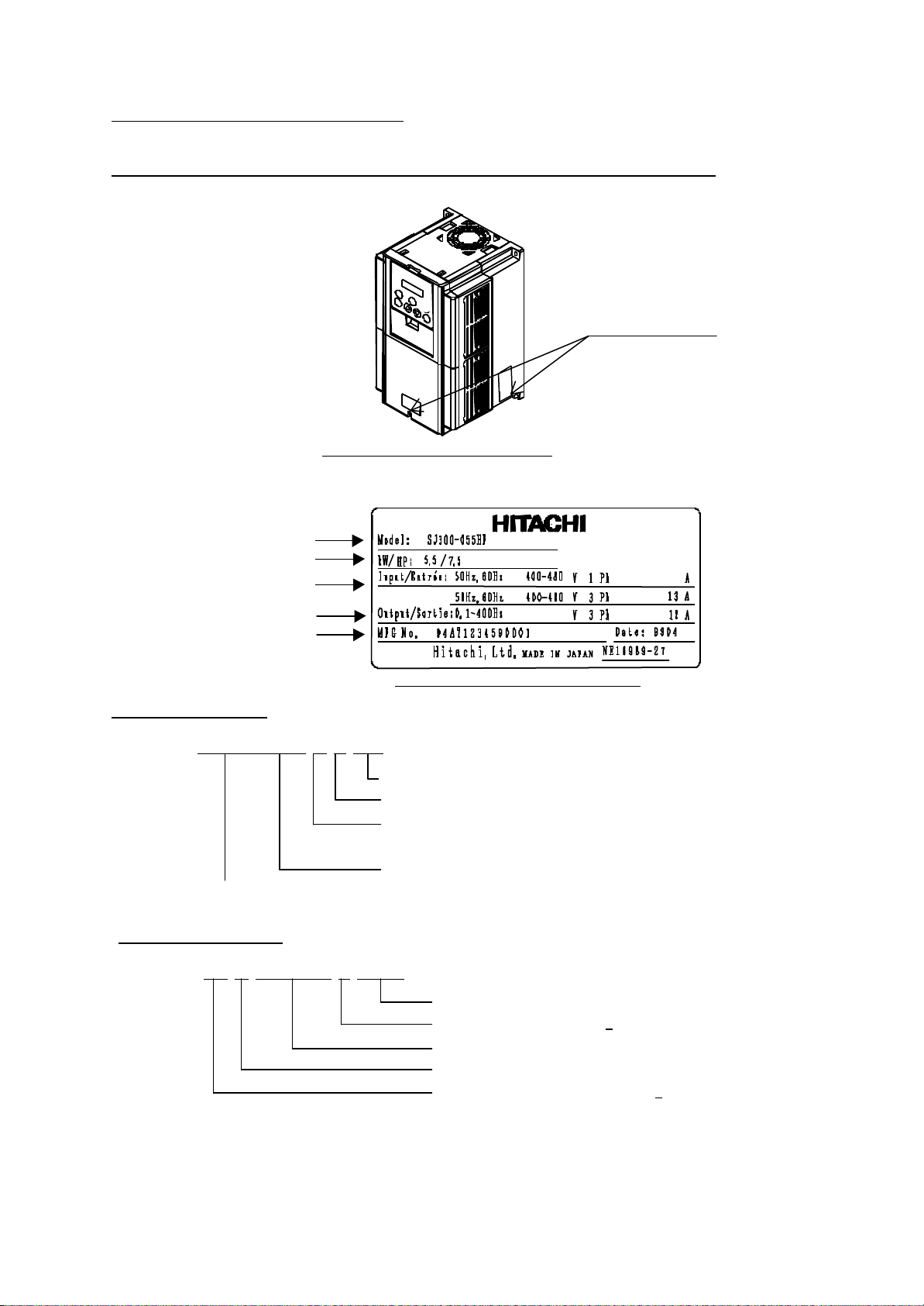
1.1 Specification label (Model name, Manufacturing number ; MFG)
• There are 2 specification label attached to the inverter as shown in Fig 1-1.
Specification label
Fig 1-1 Specification label location
• Please confirm the model name and MFG number from the specification label as follows.
Model name
Applicable motor
Input ratings
Output ratings
MFG number
1.1.1 Model name
SJ300-055 H F (R)
Model name
1.1.2 MFG number
94 A T12345 9 0001
Fig 1-2 contents of specification label
R : with POT meter
F : with digital operator
L : 3φ 200V class
H : 3φ 400V class
Applicable motor (055 : 5.5kW)
Serial No. (0001 ~ 9999)
Year of production (9 : 1999)
Production No.
REV. No.(1 character or 2 characters)
Production year & month (94 : 1999 / April)
1-1
Page 5
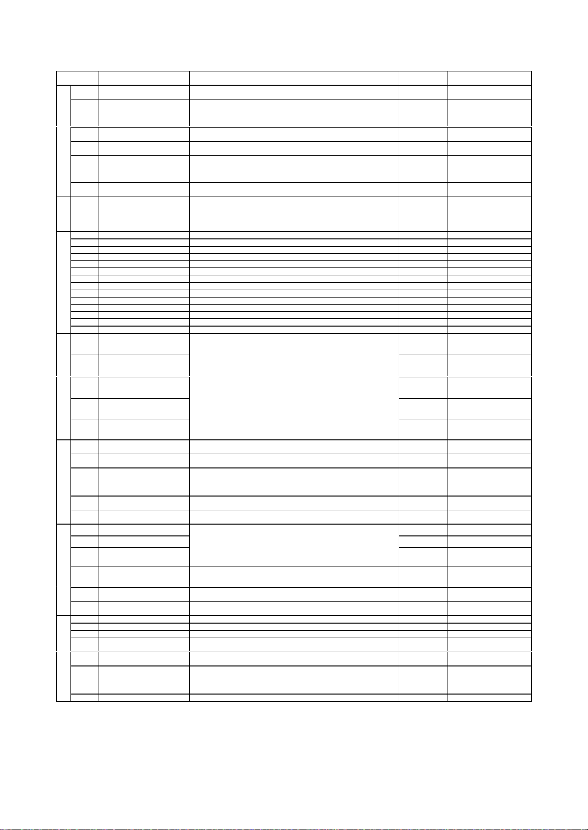
1.2 Inverter specification
F002
1
acceleration time
30.00
OFF
OFF
12
14 13
1.2.1 SJ300
Monitor Mode
Display
Function name
code
d001
d002
d003
d004
d005
d006
d007
Output frequency
monitor
Output current
monitor
Operation direction
monitor
PID feedback
monitor
Intelligent input
terminal monitor
Intelligent output
terminal monitor
Frequency
conversion monitor
0.00-99.99/100.0-400.0(Hz) -
0.0-999.9(A) F(forward)/o(stop)/r(reverse) -
0.00-99.99/100.0-999.9/1000. –9999 . /
1000-9999/ 100- 999 (10000-99900)
0.00-99.99/100.0-999.9/1000. –9999 . /
1000-3996
d012 torque monitor -300.-+300.% d013
d014
Output voltage
monitor
Input electric power
monitor
0.0-600.0 V -
0.0-999.9 kW -
Accumulated time
d016
monitor during
0.-9999./1000-9999/ 100- 999 h -
RUN
d017
d080
Power ON time
monitor
Number of trip time
monitor
0.-9999./1000-9999/ 100- 999 h -
0.-9999./1000-6553(10000-65530) (time) -
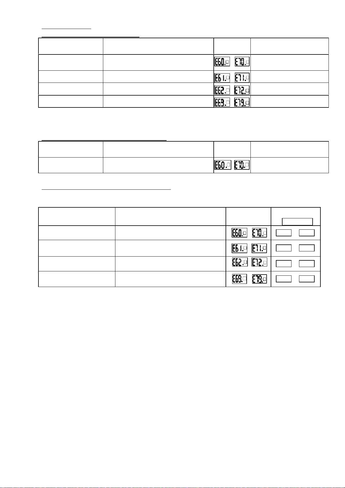
d081 Trip monitor 1 d082 Trip monitor 2 d083 Trip monitor 3 d084 Trip monitor 4 -
Trip Code , frequency(Hz), current(A),
voltage(V),RUN time(h) power ON time(h)
d085 Trip monitor 5 d086 Trip monitor 6
d090 Warning monitor Warning code -
F001
F202 2
F302 3
F003 1
F203 2
F303 3
F004
Output frequency
setting
st
nd
acceleration time 0.01-99.99/100.0-999.9/1000. -3600.(s) 30.00
rd
acceleration time 0.01-99.99/100.0-999.9/1000. -3600.(s) 30.00
st
deceleration time 0.01-99.99/100.0-999.9/1000. -3600.(s) 30.00
nd
deceleration time 0.01-99.99/100.0-999.9/1000. -3600.(s) 30.00
rd
deceleration time 0.01-99.99/100.0-999.9/1000. -3600.(s) 30.00
Operation direction
selection
0.0, starting frequency-Max. frequency
(2nd max. 3rd max. frequency)(Hz)
0.01-99.99/100.0-999.9/1000. -3600.(s)
00(forward)/01(reverse) 00
(Note1) Change mode during run by selection of b031 (software lock selection).
(Note2) Do not forget to press “STR” key when you change the display.
SJ300 monitor or data range
(digital operator)
FW
AL 15
(Example) FW, terminal 7,2, 1: ON
Terminal 8,6,5,4,3:OFF
ON
(Example) Terminal 12,11:ON
AL, 15,14,13:OFF
ON
Initial
data
0.00
(Note1)
Note
-
-
-
-
-
1–2
Page 6
Function Mode
Base setting
Code Function name SJ300 Setting range
A001 Frequency setting selection 01(terminal)/02(operator)/03(RS485)/04(option1)/05(option2) 01/01/02
A002 Operation setting selection 01(terminal)/02(operator)/03(RS485)/04(option1)/05(option2) 01/01/02
A003 Base frequency 30. - Maximum. frequency(Hz) 50./60./60.
A203 Base frequency, 2nd motor 30. – 2nd M aximum. frequency (Hz) 50./60./60.
A303 Base frequency, 3rd motor 30. - 3rd M aximum. frequency (Hz) 50./60./60.
A004 Maximum frequency 30. – 400. (Hz) 50./60./60.
A204 Maximum frequency, 2nd motor 30. – 400. (Hz) 50./60./60.
A304 Maximum frequency, 3rd motor 30. – 400. (Hz) 50./60./60.
A005 AT terminal selection
A006 02 selection
00( Changing of O and OI with AT terminal)/
01(Changing of O and O2 with AT terminal)
00(single)/01(auxiliary speed of O, OI) [no reversible] /
02(auxiliary speed of O, OI [reversible]
A011 0 start 0.00-99.99/100.0-400.0 (Hz) 0.00
A012 0 end 0.00-99.99/100.0-400.0 (Hz) 0.00
A013 0 start rate 0.-100.0 (%) 0.
Analog input setting
A014 0 end rate 0.-100.0(%) 100.
A015 0 start selection 00 (external starting frequency)/01(0Hz) 01
A016 O, OI, O2 sampling 1.-30.(times) 8.
A019 Multi-speed selection
00(binary : range is to 16 stage speed with 4 terminals)/
01(bit : range is to 8 stage speed with 7 terminals)
A020 Multi-speed 0 0.00, starting frequency-maximum. frequency(Hz) 0.00
A220 Multi-speed 0, 2nd motor 0.00, starting frequency-2nd maximum frequency(Hz) 0.00
A320 Multi-speed 0, 3rd motor 0.00, starting frequency-3rd maximum frequency(Hz) 0.00
A021 Multi-speed1 0.00, starting frequency-maximum frequency(Hz) 0.00
A022 Multi-speed2 0.00, starting frequency-maximum frequency(Hz) 0.00
A023 Multi-speed3 0.00, starting frequency-maximum frequency(Hz) 0.00
A024 Multi-speed4 0.00, starting frequency-maximum frequency(Hz) 0.00
A025 Multi-speed5 0.00, starting frequency-maximum frequency(Hz) 0.00
A026 Multi-speed6 0.00, starting frequency-maximum frequency(Hz) 0.00
A027 Multi-speed7 0.00, starting frequency-maximum frequency(Hz) 0.00
A028 Multi-speed8 0.00, starting frequency-maximum frequency(Hz) 0.00
A029 Multi-speed9 0.00, starting frequency-maximum frequency(Hz) 0.00
A030 Multi-speed10 0.00, starting frequency-maximum frequency(Hz) 0.00
A031 Multi-speed11 0.00, starting frequency-maximum frequency(Hz) 0.00
Multistage speed,jogging frequency setting
A032 Multi-speed12 0.00, starting frequency-maximum frequency(Hz) 0.00
A033 Multi-speed13 0.00, starting frequency-maximum frequency(Hz) 0.00
A034 Multi-speed14 0.00, starting frequency-maximum frequency(Hz) 0.00
A035 Multi-speed15 0.00, starting frequency-maximum frequency(Hz) 0.00
A038 Jogging frequency 0.00, starting frequency-9.99(Hz) 1.00
00(free-run on JG stop / invalid on running) / 01(stop decelerating on
JG stop / invalid on running) / 02(DC braking on JG stop/invalid on
A039 Jogging selection
running) / 03(free-run on JG stop/valid on running[JG after stop
decelerating]) / 04 (stop decelerating on JG stop/valid on running) / 05
(DC braking on JG stop/valid on operating)
A041 Torque boost selection 00 (manual torque boost) / 01 (automatic torque boost) 00
Torque boost selection, 2
A241
motor
nd
00 (manual torque boost) / 01 (automatic torque boost) 00
A042 Manual torque boost 0.0-20.0(%) 1.0
A242 Manual torque boost, 2nd motor 0.0-20.0(%) 1.0
A342 Manual torque boost, 3rd motor 0.0-20.0(%) 1.0
A043 Manual torque boost point 0.0-50.0(%) 5.0
V/f characteristic
Manual torque boost point, 2
A243
motor
Manual torque boost point, 3
A343
motor
A044 1st control
nd
rd
0.0-50.0(%) 5.0
0.0-50.0(%) 5.0
00/(VC)/01(VP1.7power)/02(free V/f setting)/03(SLV)/
04(0Hz-SLV)/05(V2)
A244 2nd control 00/(VC)/01(VP1.7power)/02(free V/f setting) /03(SLV)/04(0Hz-SLV) 00
A344 3rd control 00/(VC)/01(VP1.7power) 00
A045 Output voltage gain 20. - 100. 100.
A051 DC braking selection 00(invalid)/01(valid) 00
A052 DC braking frequency 0.00-60.00(Hz) 0.50
A053 DC braking wait time 0.0 - 5.0(s) 0.0
A054 DC braking power 0. - 100. (%) <0.-80.(%)> 0.
A055 DC braking time 0.0 - 60.0(s) 0.0
A056 DC braking edge/level selection 00(edge action)/01(level action) 01
Direct current braking
A057 DC braking power (starting time) 0. - 100. (%) <0.-80.(%)> 0.
A058 DC braking time(starting time) 0.00-60.0(s) 0.0
A059 DC carrier frequency 0.5-15(kHz) Derating <0.5-10kHz> 5.0<3.0>
(Note) < > indicate the setting range of 75 to 150kW
Initial data
-FE/-FU/-F
00
00
00
00
00
Note
1- 3
Page 7
Function Mode
A061
A261
0.00, 2
nd
frequency lower limiter-2
nd
setting maximum frequency(Hz)
A062
A262
A064
A065
A066
A067
A068
A069
A072
A073
A074
A075
A076
A081
(230/460)/
(200/400)
A085
A092
A093
A293
A393
A094
A095
A096
A097
A102
A103
A104
A105
A111
A112
A114
A131
b003
b007
Upper and lower
limiter,jump
frequency
Operation mode/ adjustable function
External frequency
Accel,
Decel
Instantaneous power failure
Code Function name SJ300 Setting range
1st frequency maximum limiter 0.00, 1st frequency lower limitter - maximum frequency(Hz) 0.00
2nd frequency maximum limiter
1st frequency minimum limiter 0.00, start frequency-maximum frequency(Hz) 0.00
2nd frequency minimum limiter 0.00, start frequency-2nd setting maximum frequency(Hz) 0.00
A063 Jump frequency1 0.00-99.99/100.0-400.0(Hz) 0.00
Jump frequency Widt h 1 0.00-10.00(Hz) 0.50
Jump frequency2 0.00-99.99/100.0-400.0(Hz) 0.00
Jump frequency Widt h 2 0.00-10.00(Hz) 0.50
Jump frequency3 0.00-99.99/100.0-400.0(Hz) 0.00
Jump frequency Widt h 3 0.00-10.00(Hz) 0.50
Acceleration stop frequency 0.00-99.99/100.0-400.0(Hz) 0.00
A070 Acceleration stop time 0.00-60.0(s) 0.0
A071 PID selection 00(invalid)/01(valid) 00
PID-P gain 0.2-5.0 1.0
PID-I gain 0.0-3600.(s) 1.0
PID-D gain 0.00-100.0(s) 0.00
PID controlAVR
adjustment
restart
PID scale 0.01-99.99(%) 1.00
PID feedback selection 00(feedback : OI)/01(feedback : O) 00
AVR selection 00(ON always)/01(OFF always)/02(OFF on decelerating) 00/00/02
A082 Motor voltage selection 200/215/220/230/240, 380/400/415/440/460/480
Operation mode selection 00(normal operation)/01(energy-saving operation)/02(Fuzzy) 00
Energy-saving response-
A086
accuracy adjustment
Acceleration time2 0.01-99.99/100.0-999.9/1000.-3600.(s) 15.00
A292 Acceleration time2(2nd motor) 0.01-99.99/100.0-999.9/1000.-3600.(s) 15.00
A392 Acceleration time2(3rd motor) 0.01-99.99/100.0-999.9/1000.-3600.(s) 15.00
Deceleration time2 0.01-99.99/100.0-999.9/1000.-3600.(s) 15.00
Deceleration time2(2nd motor) 0.01-99.99/100.0-999.9/1000.-3600.(s) 15.00
Deceleration time2(3rd motor) 0.01-99.99/100.0-999.9/1000.-3600.(s) 15.00
2nd stage adjustable selection 00(change with 2CH terminal)/01(change with setting) 00
2nd stage adjustable
A294
selection(2nd motor)
2nd acceleration frequency 0.00-99.99/100.0-400.0(Hz) 0.00
2nd acceleration
A295
frequency(2nd motor)
2nd deceleration frequency 0.00-99.99/100.0-400.0(Hz) 0.00
2nd deceleration frequency
A296
(2nd motor)
Acceleration pattern selection 00(straight line)/01(S-curve)/02(U-curve)/03(reverse U-curve) 00
A098 Deceleration pattern selection 00(straight line)/01(S-curve)/02(U-curve)/03(reverse U-curve) 00
A101 OI start 0.00-99.99/100.0-400.0(Hz) 0.00
OI end 0.00-99.99/100.0-400.0(Hz) 0.00
OI start rate 0.-100. (%) 20.
OI end rate 0.-100. (%) 100.
OI start selection 00(external start frequency)/01(0Hz) 01
O2 start -400.--100./-99.9-0.00-99.9/100.-400.(Hz) 0.00
O2 end -400.--100./-99.9-0.00-99.9/100.-400.(Hz) 0.00
A113 O2 start rate -100. - 100. (%) -100.
O2 end rate -100. - 100. (%) 100.
Acceleration curve constant 01(small swelling)-10(large swelling) 02
A132 Deceleration curve constant 01(small swelling-10(large swelling) 02
b001 Retry selection
Allowable under-voltage power
b002
failure time
Retry wait time 0.3-100.(s) 1.0
Instantaneous power failure/
b004
under-voltage trip during stop
Instantaneous power failure/
b005
under-voltage retry time
selection
b006 Open-phase selection 00(invalid)/01(valid) 00
Frequency setting to match 0.00-99.99/100.0-400.0(Hz) 0.00
00(change with 2CH terminal)/01(change with setting) 00
00(trip)/01(0Hz start)/02(start after equal frequency)/
03(trip after equaling frequency and deceleration stop)
00(invalid/01(valid)/02(invalid during stop and deceleration by stop
0.0-100.0 50.0
0.00-99.99/100.0-400.0(Hz) 0.00
0.00-99.99/100.0-400.0(Hz) 0.00
0.3-1.0(s) 1.0
command)
00(16 times)/01(free) 00
Initial data
-FE/-FU/-F
0.00
(230/400)/
00
00
Note
1- 4
Page 8
Function mode
b100
b101
b102
b103
b104
b107
b108
b109
b110
b111
b112
Free V/f setting
Intelligent input terminal setting
Overload limit
Code Function name SJ300 Setting range
b012 Electronic thermal level 0.2*constant current-1.20*constant current(A)
Electronic thermal level
b212
(2nd motor)
Electronic thermal level
b312
(3rd motor)
1st electronic thermal
b013
characteristic selection
2nd electronic thermal
b213
characteristic selection
3rd electronic thermal
b313
characteristic selection
Free electronic thermal
b015
Electronic thermal
frequency 1
Free electronic thermal
b016
current 1
Free electronic thermal
b017
frequency 2
Free electronic thermal
b018
current 2
Free electronic thermal
b019
frequency 3
Free electronic thermal
b020
current 3
b021 Overload restriction selection
b022 Overload restriction level 0.50* rated current-2.00* rated current(A) <-1.80*ratede current(A)>
Overload restriction limit
b023
constant
Overload restriction 2
b024
selection
b025 Overload restriction level 2 0.50*rated current-2.00*rated current(A) <-1.80*rated current(A)>
Overload restriction constant
b026
2
b031 Software lock mode selection
Free V/f frequency 1 0.- Free V/f frequency2(Hz) 0.
Free V/f voltage 1 0.-800.0(V) 0.0
Free V/f frequency 2 0.- Free V/f frequency3(Hz) 0.
Free V/f voltage 2 0.-800.0(V) 0.0
Free V/f frequency 3 0.- Free V/f frequency4(Hz) 0.
b105 Free V/f voltage 3 0.-800.0(V) 0.0
b106 Free V/f frequency 4 0.- Free V/f frequency5(Hz) 0.
Free V/f voltage 4 0.-800.0(V) 0.0
Free V/f frequency 5 0.- Free V/f frequency6(Hz) 0.
Free V/f voltage 5 0.-800.0(V) 0.0
Free V/f frequency 6 0.- Free V/f frequency7(Hz) 0.
Free V/f voltage 6 0.-800.0(V) 0.0
Free V/f frequency 7 0.-400.(Hz) 0.
b113 Free V/f voltage 7 0.-800.0(V) 0.0
C001 Intelligent input 1 setting 18
C002 Intelligent input 2 setting 16
C003 Intelligent input 3 setting 06
C004 Intelligent input 4 setting 11
C005 Intelligent input 5 setting 09
C006 Intelligent input 6 setting 03/13/03
C007 Intelligent input 7 setting 02
C008 Intelligent input 8 setting
02(enabled on constant speed)/03(enabled on acceleration / constant
02(enabled on constant speed)/03(enabled on acceleration / constant
00(impossible to change the data except this item when SFT terminal is
ON)/01(impossible to change the data except setting frequency item
when SFT terminal is ON)/02(impossible to change the data except this
item)/
03(impossible to change the data except setting frequency item)/
10(possible to change data on operating)
01/(RV:Reverse is valid)/02(CF1:Multi-speed1)/ 03(CF2:Multi-speed2)/
04(CF3:Multi-speed3)/ 05(CF4:Multi-speed4)/ 06(JG:Jogging)/
07(DB:External DC braking)/ 08(SET:2nd control)/
09(2CH:two-stage adjustable speed)/ 11(FRS:Free-run)/ 12( EXT:External trip)/
13(USP:Unattended start protection)/ 14(CS:commercial change)/
15(SFT:software lock)/ 16(AT:Analog input voltage/current select)/
17(SET3:3rdcontrol)/ 18(RS:Reset inverter)/ 20(STA:3wire run)/
21(STP:3wire keep)/ 22(F/R:3wire forward/reverse)/
23(PID:PID selection valid/invalid)/ 24(PIDC:PID integrating reset)/
26(CAS:Control gain switch function)/ 27(UP:Remote control UP function)/
28(DWN:Remote control DOWN function)/29( UDC:Remote control data clear)/
31(OPE:Operating by operator select)/ 32(SF1:Multi-speed bit1)/
33(SF2:Multi-speed bit2)/ 34(SF3:Multi-speed bit3)/ 35(SF4:Multi-speed bit4)/
36(SF5:Multi speed bit5)/ 37(SF6:Multi-speed bit6)/ 38(SF7:Multi-speed bit7)/
39(OLR:Overload restriction change) / 40(TL:Torque limit select)/
41(TRQ1:Torque limit switch 1)/ 42(TRQ2:Torque limit switch 2)/
43((PPI:P/PI switch)/ 44(BOK:Braking comformation)/ 45(ORT:Orientation)/
46(LAC:LAD cancel)/ 47(PCLR:Position error clear)/
48(STAT:Permission of pulse train)/ no(NO:No assign)
0.2*constant current-1.20*constant current(A)
0.2*constant current-1.20*constant current(A)
00(reduced characteristic)/ 01(constant torque characteristic)/
00(reduced characteristic)/ 01(constant torque characteristic)/
00/(reduced characteristic)01(constant torque characteristic)/
00(invalid)/01(enabled on acceleration / constant speed)/
speed (speed increasing at regenerating mode))
00(invalid)/01(enabled on acceleration / constant speed)/
speed (speed increasing at regenerating mode))
02(free setting)
02(free setting)
02(free setting)
0.-400.(Hz) 0.
0.0-1000.(A) 0.0
0.-400.(Hz) 0.
0.0-1000. (A) 0.0
0.-400.(Hz) 0.
0.0-1000.(A) 0.0
0.10-30.00(s) 1.00
0.10-30.00(s) 1.00
(Note) < > indicate the setting range of 75 to 150kW
Initial data
-FE/-FU/-F
Rated
Current of
inverter
Rated
Current of
Inverter
Rated
current of
inverter
01/01/00
01/01/00
01/01/00
01
Rated current
of Inverter
x 1.50
01
Rated current
of inverter
x1.50
01
01
Note
1- 5
Page 9
Function mode
C033
C034
C035
C036
C044
C062
C070
C072
C073
C075
C078
Communication waiting time
C085
Analog meter setting
Input terminal setting
intelligent
Output terminal state
Communication
function adjustment
Code Function name SJ300 Setting range
Intelligent input 1 a/b
C011
(NO/NC) selection
Intelligent input 2 a/b
C012
(NO/NC) selection
Intelligent input 3 a/b
C013
(NO/NC) selection
Intelligent input 4 a/b
C014
(NO/NC) selection
Intelligent input 5 a/b
C015
(NO/NC) selection
Intelligent input 6 a/b
C016
(NO/NC) selection
Intelligent input 7a/b
C017
(NO/NC) selection
Intelligent input 8 a/b
C018
(NO/NC) selection
Input FW a/b (NO/NC)
C019
Selection
C021 Intelligent output 11 setting 01
C022 Intelligent output 12 setting 00
C023 Intelligent output 13 setting 03
C024 Intelligent output 14 setting 07
C025 Intelligent output 15 setting 08
C026 Alarm relay output
Intelligent output terminal setting
C027 FM selection
C028 AM selection
C029 AMI selection
C031 Intelligent output 11 a/b 00(NO)/01(NC) 00
C032 Intelligent output 12 a/b 00(NO)/01(NC) 00
Intelligent output 13 a/b 00(NO)/01(NC) 00
Intelligent output 14 a/b 00(NO)/01(NC) 00
Intelligent output 15 a/b 00(NO)/01(NC) 00
Alarm relay output a/b 00(NO)/01(NC) 01
Overload advance notice
C040
signal output mode
Overload advance notice
C041
level
Frequency arrival setting for
C042
acceleration.
Arrival frequency setting for
C043
deceleration .
PID deviation setting level 0.0-100.0(%) 3.0
Frequency arrival setting for
C045
acceleration 2.
setting,Output level setting
Arrival frequency setting for
C046
deceleration 2.
Over torque level setting
C055
(Forward-driving)
Over torque level setting
C056
(Reverse-regenerating)
Over torque level setting
C057
(Reverse-driving)
Over torque level setting
C058
(Forward-regenerating)
Thermal warning level
C061
setting
Alarm code selection 00(Invalid)/01(3bit)/02(4bit) 00
Zero speed detection level
C063
setting
Data command 02(operator)/03(RS485)/04(option1)/05(option2) 02
Communicating transmission
C071
speed
Communication code 1. -32. 1.
Communication bit 7(7bit)/8(8bit) 7
00(RUN:running)/01(FA1:Frequency arrival type1 signal)/
02(FA2:over setting frequency)/03( OL:Overload advance notice signal)/
04( OD:Output deviation for PID control)/05( AL:Alarm signal)/
06(FA3:Only setting frequency)/07( OTQ:Over-torque signal)/
08( IP:On instantaneous stop)/09(UV:Under voltage)/
10(TRQ:Torque limit)/11(RNT:RUN time over/12(ONT:ON time over)/
13(THM:thermal caution)/19(BRK:Brake release signal)/
20( BER:Brake error signal)/21( ZS:Zero speed detect signal)/
22(DSE:Speed error over signal)/23( POK:Positioning completion signal)
24(FA4:Over frequency 2 signal)/25(FA5:Only setting frequency)/
26(OL2: Overload advance notice signal 2)
(Intelligent output terminal 11-13 or 11-14 becomes AC0-AC2 or AC0-AC3
(Can:Alarm cord output) forcibly when alarm cord output is selected in
C062)
00(Output frequency)/01(Output current) /02(Output torque)/
03(Digital output frequency)/04(Output voltage)/
05(Input electric power)/06(thermal load rate)/07(LAD frequency)
00(Output frequency)/01(Output current)/02(Output torque)/
04(Output voltage)/05(Input electric power)/06(thermal load rate)/
07(LAD frequency)
00(Output frequency)/01(Output current)/02(Output torque)/
04(Output voltage)/05(Input electric power)/
06(Thermal load rate)/07(LAD frequency)
00(On accel. And decel, constant speed)/01(Only constant speed) 01
03(2400bps)/04(4800bps)/05(9600bps)/06(19200bps)
C074 Communication parity 00(no parity name)/01(even parity)/02(odd parity) 00
Communication stop bit 1(bit)/2(bit) 1
C081 O adjustment 0.-9999./1000-6553(10000-65530)
C082 OI adjustment 0.-9999./1000-6553(10000-65530)
C083 O2 adjustment 0.-9999./1000-6553(10000-65530)
Thermistor adjustment 0.0 - 1000. 105.0
C086 AM offset adjustment 0.0 - 10.0(V) 0.0
C087 AMI adjustment 0. - 255. 80
C088 AMI offset adjustment 0. - 20.0( mA) 4.0
(Note) < > indicate the setting range of 75 to 150kW
00(NO)/01(NC) 00
00(NO)/01(NC) 00
00(NO)/01(NC) 00
00(NO)/01(NC) 00
00(NO)/01(NC) 00
00(NO)/01(NC) 00/01/00
00(NO)/01(NC) 00
00(NO)/01(NC) 00
00(NO)/01(NC) 00
0.0-2.0*rated current(A)
0.00-99.99/100.0-400.0(Hz) 0.00
0.00-99.99/100.0-400.0(Hz) 0.00
0.00-99.99/100.0-400.0(Hz) 0.00
0.00-99.99/100.0-400.0(Hz) 0.00
0.-200.(%) <0.-180.> 100.
0.-200.(%) 100.
0.-200.(%) <0.-180.> 100.
0.-200.(%) <0.-180.> 100.
0.-100.(%) <0.-180.> 80.
0.00-99.99/100.(Hz) 0.00
02(loop-back test)
0.-1000.(ms) 0.
Initial data
-FE/-FU/-F
05
00
00
00
Inverter
rated current
04
Setting on
forwarding
Setting on
forwarding
Setting on
forwarding
Note
1- 6
Page 10
Function mode
b034
b037
b045
Torque LAD-STOP selection
b080
b081
b083
5.0 <3.0>
b085
Country code for initialization
01/02/00
b087
b090
b091
01(ON during run, After power ON, then for 5 minutes on stop is implied.)
b095
b096
b098
b122
Waiting time for acceleration
b123
b125
C091
C101
The others
Code Function name SJ300 Setting range
(Note) < > indicate the setting range of 75 to 150kW
RUN time/Power ON time level
b035 Operation direction restrict 00(Reverse is valid)/01(Only forward)/02(Only reverse) 00
b036 Start reduced voltage 00(Start reduced voltage time small)-06(Start reduced voltage time large) 06
Display selection 00(all display)/01(each function display)/02(User setting / main setting) 00
b040 Torque limit mode selection
Torque limit level 1 setting
b041
(Forward-driving at
4 quadrant mode)
Torque limit level 2 setting
b042
(Reverse-regenerating at
4 quadrant mode)
Torque limit level 3 setting
b043
(Reverse-driving at
4 quadrant mode)
Torque limit level 4 setting
b044
(Forward-regenerating at
4 quadrant mode)
Reverse run prevention
b046
selection
Selection of non-stop
b050
function at instantaneous
power failure
Start voltage of non-stop
b051
function setting
OV LAD-STOP level of non-
b052
stop function setting
Deceleration time of non-
b053
stop function setting
Deceleration frequency widt h
b054
of non-stop function setting
AM adjustment 0. - 255. 180
FM adjustment 0. - 255. 60
b082 Start frequency adjustment 0.10-9.99(Hz) 0.50
Carrier frequency setting 0.5-15.0(kHz) Derating enable, <0-10kHz>
b084 Initialize mode
Frequency scalar conversion
b086
factor
STOP key enable 00(valid)/01(invalid) 00
Resume on FRS cancellation
b088
mode
BRD usage ratio 0.0-100.0(%) 0.0
Stop mode selection 00(deceleration stop)/01(Free-run stop) 00
b092 Cooling fan control
BRD selection 00(invalid)/01(valid<invalid during stop>)/02(valid<valid during stop>) 00
BRD ON level 330-380/660-760(V) 360/720
Thermistor selection 00(invalid)/01(Positive temperature coefficient enable)/02 (NTC enable) 00
b099 Thermistor error level 0. - 9999. (ohm) 3000.
b120 Braking control selection 00(Invalid)/01(valid) 00
Waiting time for releasing
b121
braking conformation
Waiting time for stop 0.00-5.00(s) 0.00
Waiting time for signal
b124
conformation
Releasing frequency 0.00-99.99/100.0-400.0(Hz) 0.00
b126 Releasing current 0.00*rated current-2.00*rated current(A)
Debug mode selection 00(No display)/01(Display) 00
UP/DWN selection 00(No frequency data)/01(Keep frequency data) 00
C102 Reset selection
Reset f frequency matching
C103
selection
Overload advance notice
C111
level
C121 O zero adjustment 0.-9999./1000-6553(10000-65530)
C122 OI zero adjustment 0.-9999./1000-6553(10000-65530)
C123 O2 zero adjustment 0.-9999./1000-6553(10000-65530)
0.-9999./1000-6553(10000-65530)hr 0.
00(4 quadrant mode)/01(Terminal operation)/
02(Analog input)/03(Option1)/04(Option2)
0.-200.(%)/no(Invalid) <0.-180.(%)/no(Invalid)> 150.
0.-200.(%)/no(Invalid) <0.-180.(%)/no(Invalid)> 150.
0.-200.(%)/no(Invalid) <0.-180.(%)/no(Invalid)> 150.
0.-200.(%)/no(Invalid) <0.-180.(%)/no(Invalid)> 150.
00(Invalid)/01(Valid) 00
00(Invalid)/01(Valid) 00
00(Invalid)/01(Valid) 00
0.0-1000.(V) 0.0
0.0-1000.(V) 0.0
0.01-99.99/100.0-999.9/1000.-3600.(s) 1.00
0.00-10.00(Hz) 0.00
00(Trip history clear)/01(Data initialization)/
02(Trip history clear + data initialization)
00(Interior)/01(EC)/02(USA)
0.1-99.9 1.0
00(0Hz start)/01(Start f-equaling) 00
00(Always ON)/
0.00-5.00(s) 0.00
0.00-5.00(s) 0.00
0.00-5.00(s) 0.00
00(Trip cancel during ON)/01(Trip cancel during OFF)/
02(Valid only during trip<Cancel during ON>)
00(0Hz start)/01(Start f-equaling) 00
0.0-2.0*rated current(A)
Initial data
-FE/-FU/-F
00
00
00
Rated
current of
inverter
00
Inverter
rated
current
Set on
forwarding
Set on
forwarding
Set on
forwarding
Note
1- 7
Page 11
Function mode
forwarding
forwarding
H004
H204
H005
H205
H006
H060
H260
The others
Code Function name SJ300 Setting range
H001 Autotuning selection
H002 1st motor constant selection
H202 2nd motor constant selection
H003 1st allowable motor selection 0.20-75.0(kW) <0.2-160(kW)>
H203 2nd allowable motor selection 0.20-75.0(kW) <0.2-160(kW)>
1st motor pole selection 2/4/6/8(pole) 4
2nd motor pole selection 2/4/6/8(pole) 4
1st speed response setting 0.001-9.999/10.00-65.53 1.590
2nd speed response setting 0.001-9.999/10.00-65.53 1.590
1st stabilized factor 0. - 255. 100.
H206 2nd stabilized factor 0. - 255. 100.
H306 3rd stabilized factor 0. - 255. 100.
H020 1st motor constant R1 0.000-9.999/10.00-65.53(ohm)
H220 2nd motor constant R1 0.000-9.999/10.00-65.53(ohm)
H021 1st motor constant R 2 0.000-9.999/10.00-65.53(ohm)
H221 2nd motor constant R2 0.000-9.999/10.00-65.53(ohm)
H022 1st motor constant L 0.00-99.99/100.0-655.3( mH)
H222 2nd motor constant L 0.00-99.99/100.0-655.3( mH)
H023 1st motor constant I0 0.00-99.99/100.0-655.3(A)
H223 2nd motor constant I0 0.00-99.99/100.0-655.3(A)
H024 1st motor constant J
H224 2nd motor constant J
1st motor constant R1
H030
(Autotuning data)
2nd motor constant R1
H230
(Autotuning data)
1st motor constant R 2
H031
(Autotuning data)
2nd motor constant R2
H231
(Autotuning data)
1st motor constant L
H032
(Autotuning data)
2nd motor constant L
H232
(Autotuning data)
1st motor constant I0
H033
(Autotuning data)
2nd motor constant I0
H233
(Autotuning data)
H034 1st motor constant J 0.001-9.999/10.00-99.99/100.0-9999.( kgm2)
H234 2nd motor constant J 0.001-9.999/10.00-99.99/100.0-9999.( kgm2)
1st PI-control proportion gain
H050
setting
2nd PI -control proportion gain
H250
setting
1st PI-control integration gain
H051
setting
2nd PI -control integration gain
H251
setting
1st P-control proportion gain
H052
setting
2nd P-control proportion gain
H252
setting
1st 0Hz-SLV limiter setting 0.-100.(%) 100.
2nd 0Hz-SLV limiter setting 0.-100.(%) 100.
PI-control proportion gain for
H070
switching
PI-control integration gain for
H071
switching
P-control proportion gain for
H072
switching
(Note) < > indicate the setting range of 75 to 150kW
00(Invalid)/01( Valid(the motor does not rotate) )/
00(Hitachi general purpose motor data )/01(Autotuning data)/
00(Hitachi general purpose motor data )/01(Autotuning data)/
02( Valid(the motor rotates))
02( Autotuning data with online autotuning)
02( Autotuning data with online autotuning)
0.001-9.999/10.00-99.99/100.0-9999.( kgm2)
0.001-9.999/10.00-99.99/100.0-9999.( kgm2)
0.000-9.999/10.00-65.53(ohm)
0.000-9.999/10.00-65.53(ohm)
0.000-9.999/10.00-65.53(ohm)
0.000-9.999/10.00-65.53(ohm)
0.00-99.99/100.0-655.3( mH)
0.00-99.99/100.0-655.3( mH)
0.00-99.99/100.0-655.3(A)
0.00-99.99/100.0-655.3(A)
0.00-99.99/100.0-999.9/1000.(%) 100.0
0.00-99.99/100.0-999.9/1000.(%) 100.0
0.00-99.99/100.0-999.9/1000.(%) 100.0
0.00-99.99/100.0-999.9/1000.(%) 100.0
0.01-10.00 1.00
0.01-10.00 1.00
0.00-99.99/100.0-999.9/1000.(%) 100.0
0.00-99.99/100.0-999.9/1000.(%) 100.0
0.00-10.00 1.00
Initial data
-FE/-FU/-F
00
00
00
Set on
Set on
Set on
forwarding
Set on
forwarding
Set on
forwarding
Set on
forwarding
Set on
forwarding
Set on
forwarding
Set on
forwarding
Set on
forwarding
Set on
forwarding
Set on
forwarding
Set on
forwarding
Set on
forwarding
Set on
forwarding
Set on
forwarding
Set on
forwarding
Set on
forwarding
Set on
forwarding
Set on
forwarding
Set on
forwarding
Set on
forwarding
Note
1- 8
Page 12
Function mode
P010
P012
P015
U003
U004
U005
U006
U007
U008
U009
U011
U012
Option
Code Function name SJ300 Setting range
Option1 operation selection
P001
on error
Option2 operation selection
P002
on error
Feed-back option selection 00(Invalid)/01(Valid) 00
Encoder pulse number
P011
setting
Control mode selection 00(ASR mode)/01(APR mode) 00
Pulse train input mode
P013
selection
Orientation stop position
P014
setting
Orientation speed setting 0.00-99.99/100.0-120.0(Hz) 5.00
Orientation direction
P016
selection
Orientation completion range
P017
setting
Orientation completion delay
P018
time setting
Electronic gear position
P019
selection
Electronic gear numerator of
P020
ratio setting
Electronic gear denominator
P021
of ratio setting
Position control feed-forward
P022
gain setting
Position control loop gain
P023
setting
Compensation of secondary
P025
resistor selection
Over-speed detect level
P026
setting
Speed-error over detect level
P027
setting
Digital input option input
P031
mode selection ( Acc/Dec)
Stop position setting for
P032
orientation input mode
selection
DeviceNet running order of
P044
monitoring timer setting
Setting in action of abnormal
P045
communication
Output assemble instance
P046
Number setting
Input assemble instance
P047
Number setting
Detect of idol mode for
P048
motion setting
P049 Pole setting of rotation speed 0-38(even only) 0
U001 User1 selection no/d001-P049 <-P032> no
U002 User2 selection no/d001-P049 <-P032> no
User3 selection no/d001-P049 <-P032> no
User4 selection no/d001-P049 <-P032> no
User5 selection no/d001-P049 <-P032> no
User6 selection no/d001-P049 <-P032> no
User7 selection no/d001-P049 <-P032> no
User8 selection no/d001-P049 <-P032> no
User selection
User9 selection no/d001-P049 <-P032> no
U010 User10 selection no/d001-P049 <-P032> no
User11 selection no/d001-P049 <-P032> no
User12 selection no/d001-P049 <-P032> no
128.-9999./1000-6500(10000-65000) (pulse) 1024
00(Mode 0)/01(Mode 1)/02(Mode 2)/03(Mode 3) 00
00(trip)/01(trip after deceleration stop)/02(invalid)/
00(trip)/01(trip after deceleration stop)/02(invalid)/
00(TRP)/01(RUN) 00
00(TRP)/01(RUN) 00
0.-4095. 0.
00(Forward)/01(Reverse) 00
0.-9999./1000(10000) (pulse) 5
0.00-9.99(s) 0.00
00(Feedback)/01(Reference) 00
0.-9999. 1.
0.-9999. 1.
0.00-99.99/100.0-655.3 0.00
0.00-99.99/100.0 0.50
00(Invalid)/01(Valid) 00
0.00-99.99/100.0-150.0(%) 135.0
0.00-99.99/100.0-120.0(Hz) 7.50
00(operator)/01(option1)/02(option2) 00
00(operator)/01(option1)/02(option2) 00
0.00-99.99s 1.00
03(free-run)04(deceleration stop)
20,21,100 21
70,71,101 71
03(free-run)04(deceleration stop)
Initial data
-FE/-FU/-F
0.
01
Note
(Note 1) P044-P049 are displayed on a 0.4-55kW model.
1- 9
Page 13
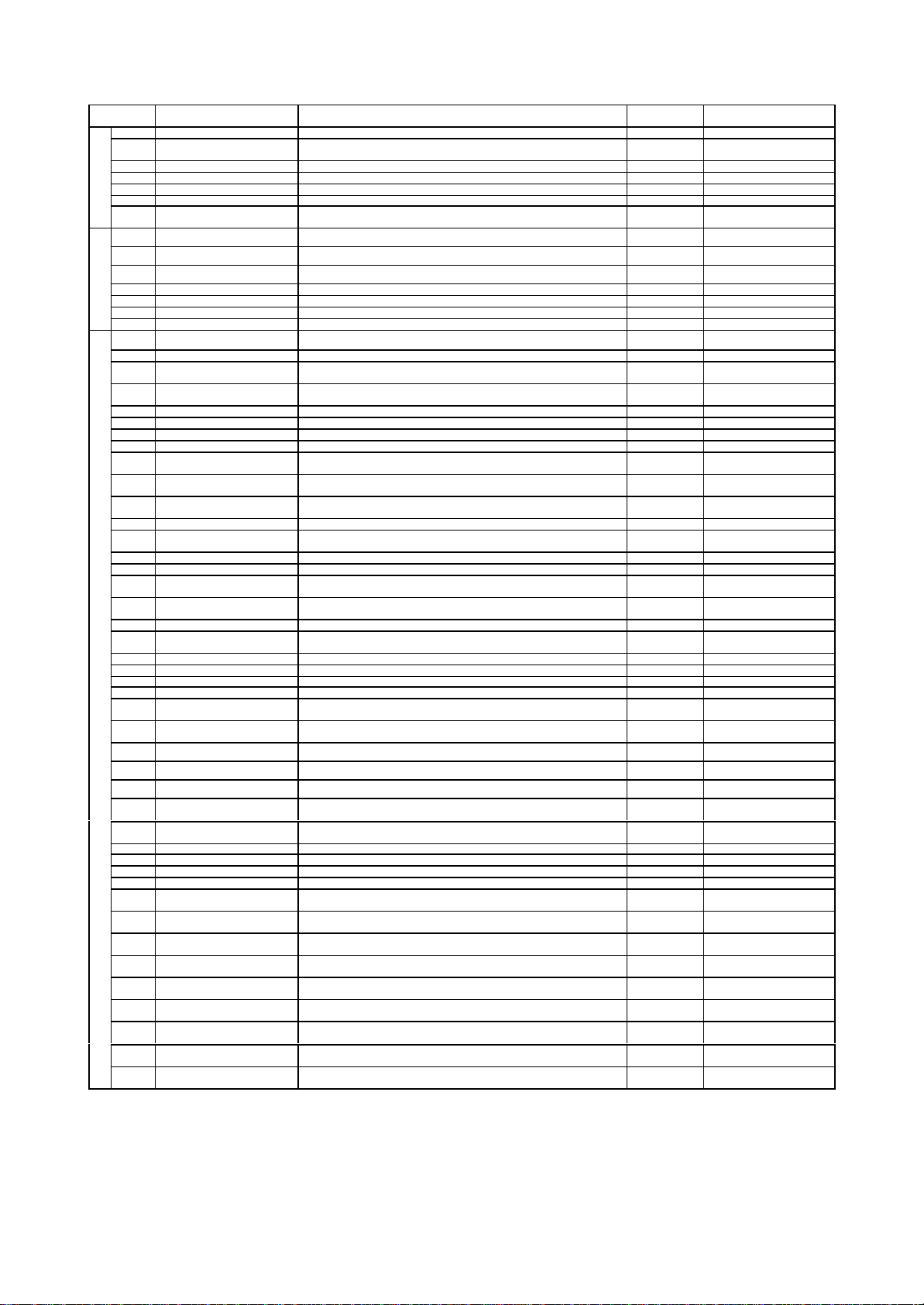
1.2.2 L300P
d090
F203
deceleration time
30.00
OFF
5 4
3 2
1
OFF
12 11
Monitor code
Display
Function name
code
d001
d002
d003
d004
d005
d006
d007
d013
d014
d016
d017
d080
d081 Trip monitor 1
d082 Trip monitor 2
d083 Trip monitor 3
d084 Trip monitor 4
d085 Trip monitor 5
d086 Trip monitor 6
Output frequency
monitor
Output current
monitor
Operation direction
monitor
PID feedback
monitor
Intelligent input
terminal monitor
Intelligent output
terminal monitor
Frequency
conversion monitor
Output voltage
monitor
Electric power
monitor
Accumulated time
monitor during RUN
Power ON time
monitor
Number of trip time
monitor
0.00-99.99/100.0-400.0(Hz) -
0.0-999.9(A) F(forward)/o(stop)/r(reverse) -
0.00-99.99/100.0-999.9/1000. -9999 . /
1000-9999/ 100- 999 (10000-99900)
0.00-99.99/100.0-999.9/1000. –9999 . /
1000-3996
0.0-600.0 V -
0.0-999.9 kW -
0.-9999./1000-9999/ 100- 999 h -
0.-9999./1000-9999/ 100- 999 h -
0.-9999./1000-6553(10000-65530) (time) Trip Code , frequency(Hz), current(A),
voltage(V),RUN time(h) power ON time(h)
Trip Code , frequency(Hz), current(A),
voltage(V),RUN time(h) power ON time(h)
Trip Code , frequency(Hz), current(A),
voltage(V),RUN time(h) power ON time(h)
Trip Code , frequency(Hz), current(A),
voltage(V),RUN time(h) power ON time(h)
Trip Code , frequency(Hz), current(A),
voltage(V),RUN time(h) power ON time(h)
Trip Code , frequency(Hz), current(A),
voltage(V),RUN time(h) power ON time(h)
Warning monitor Warning code F001
F002 1
F202 2
F003 1
F004
Output frequency
setting
st
acceleration time 0.01-99.99/100.0-999.9/1000.-3600.(s) 30.00
nd
acceleration time 0.01-99.99/100.0-999.9/1000. -3600. (s) 30.00
st
deceleration time 0.01-99.99/100.0-999.9/1000. -3600. (s) 30.00
2nd
Operation direction
selection
0.0, starting frequency-Max. frequency
(2nd max. frequency)(Hz)
0.01-99.99/100.0-999.9/1000. -3600. (s)
00(forward)/01(reverse) 00
(Note1) Change mode during run by selection of b031 (software lock selection).
(Note2) Do not forget to press “STR” key when you change the display.
L300P monitor or data range
(digital operator)
FW
AL
(Example) FW, terminal2, and 1: ON
Terminal 5, 4, 3 :OFF
ON
(Example) Terminal2, 1:ON
AL :OFF
ON
Initial
data
-
-
-
-
-
-
-
-
-
-
0.00
Note
1 -10
Page 14
Function Mode
Base setting
Multistage
V/f characteristic
Code Function name L300P Setting range
A001 Frequency setting selection
A002 Operation setting selection 01(terminal)/02(operator)/03(RS485)/04(option1)/05(option2) 01/01/02
A003 Base frequency 30. - Maximum. frequency(Hz) 50./60./60.
A203 Base frequency, 2nd motor 30. - 2nd M aximum. frequency (Hz) 50./60./60.
A004 Maximum frequency 30. - 400. (Hz) 50./60./60.
Maximum frequency, 2nd
A204
motor
A005 AT terminal selection
A006 02 selection
A011 0 start 0.00-99.99/100.0-400.0 (Hz) 0.00
A012 0 end 0.00-99.99/100.0-400.0 (Hz) 0.00
A013 0 start rate 0.-100.0 (%) 0.
A014 0 end rate 0.-100.0(%) 100.
A015 0 start selection 00 (external starting frequency)/01( OHz) 01
A016 O, OI, O2 sampling 1.-30.(times) 8.
A019 Multi-speed selection
A020 Multi-speed 0 0.00, starting frequency-maximum. frequency(Hz) 0.00
A220 Multi-speed 0, 2nd motor 0.00, starting frequency-2nd maximum frequency(Hz) 0.00
A021 Multi-speed1 0.00, starting frequency-maximum frequency(Hz) 0.00
A022 Multi-speed2 0.00, starting frequency-maximum frequency(Hz) 0.00
A023 Multi-speed3 0.00, starting frequency-maximum frequency(Hz) 0.00
A024 Multi-speed4 0.00, starting frequency-maximum frequency(Hz) 0.00
A025 Multi-speed5 0.00, starting frequency-maximum frequency(Hz) 0.00
A026 Multi-speed6 0.00, starting frequency-maximum frequency(Hz) 0.00
A027 Multi-speed7 0.00, starting frequency-maximum frequency(Hz) 0.00
A028 Multi-speed8 0.00, starting frequency-maximum frequency(Hz) 0.00
A029 Multi-speed9 0.00, starting frequency-maximum frequency(Hz) 0.00
A030 Multi-speed10 0.00, starting frequency-maximum frequency(Hz) 0.00
A031 Multi-speed11 0.00, starting frequency-maximum frequency(Hz) 0.00
A032 Multi-speed12 0.00, starting frequency-maximum frequency(Hz) 0.00
speed,jogging frequency setting
A033 Multi-speed13 0.00, starting frequency-maximum frequency(Hz) 0.00
A034 Multi-speed14 0.00, starting frequency-maximum frequency(Hz) 0.00
A035 Multi-speed15 0.00, starting frequency-maximum frequency(Hz) 0.00
A038 Jogging frequency 0.00, starting frequency-9.99(Hz) 1.00
A039 Jogging selection
A041 Torque boost selection 00 (manual torque boost) / 01 (automatic torque boost) 00
Torque boost selection, 2
A241
motor
A042 Manual torque boost 0.0-20.0(%) 1.0
A242 Manual torque boost, 2nd motor 0.0-20.0(%) 1.0
A043 Manual torque boost point 0.0-50.0(%) 5.0
Manual torque boost point, 2
A243
motor
A044 1st control 00/(VC)/01(VP1.7power)/02(free V/f setting) 00
A244 2nd control 00/(VC)/01(VP1.7power)/02(free V/f setting) 00
A045 Output voltage gain 20. - 100. (%) 100.
A051 DC braking selection 00(invalid)/01(valid) 00
A052 DC braking frequency 0.00-60.00(Hz) 0.50
A053 DC braking wait time 0.0 - 5.0(s) 0.0
A054 DC braking power 0. - 70. (%) 0.
A055 DC braking time 0.0 - 60.0(s) 0.0
DC braking edge/level
A056
selection
DC braking power
A057
Direct current braking Analog input setting
(starting time)
DC braking time
A058
(starting time)
A059 DC carrier frequency 0.5-12(kHz) Derating <0.5-8(kHz)> 3.0
00( Changing of O and OI with AT terminal)/01(Changing of O and O2
00(binary : range is to 16 stage speed with 4 terminals)/01(bit : range
00(free-run on JG stop / invalid on running) / 01(stop decelerating on
JG stop / invalid on running) / 02(DC braking on JG stop/invalid on
running) / 03(free-run on JG stop/valid on running[JG after stop
decelerating]) / 04 (stop decelerating on JG stop/valid on running) /
05 (DC braking on JG stop/valid on operating)
nd
nd
00(VR)/01(terminal)/02(operator)/03(RS485)/
04(option1)/05(option2)
30. - 400. (Hz) 50./60./60.
with AT terminal)
00(single)/01(auxiliary speed of O, OI) [no reversible]
/02(auxiliary speed of O, OI [reversible]
is to 6 stage speed with 5 terminals)
00 (manual torque boost) / 01 (automatic torque boost) 00
0.0-50.0(%) 5.0
00(edge action)/01(level action) 01
0. - 70. (%) 0.
0.00-60.0(s) 0.0
(Note) < > indicate the setting range of 90 to 132kW
Initial data
-FE/-FU/-FR
01/01/00
N o t e
00
00
00
00
1- 11
Page 15
Function Mode
Upper and lower
frequency
External frequency
AVR
Operation mode/ adjustable function
Accel
Decel
Instantaneous power failure
Electronic thermal
Code Function name L300P Setting range
A061 1st frequency upper limiter 0.00, 1st frequency lower limiter-maximum frequency(Hz) 0.00
A261 2nd frequency upper limiter 0.00, 2nd frequency lower limiter-2nd setting maximum
A062 1st frequency lower limiter 0.00, start frequency-maximum frequency(Hz) 0.00
A262 2nd frequency lower limiter 0.00, start frequency-2nd setting maximum frequency(Hz) 0.00
limiter / jump
A063 Jump frequency1 0.00-99.99/100.0-400.0(Hz) 0.00
A064 Jump frequency Width 1 0.00-10.00(Hz) 0.50
A065 Jump frequency2 0.00-99.99/100.0-400.0(Hz) 0.00
A066 Jump frequency Width 2 0.00-10.00(Hz) 0.50
A067 Jump frequency3 0.00-99.99/100.0-400.0(Hz) 0.00
A068 Jump frequency Width 3 0.00-10.00(Hz) 0.50
A069 Acceleration stop frequency 0.00-99.99/100.0-400.0(Hz) 0.00
A070 Acceleration stop time 0.00-60.0(s) 0.0
A071 PID selection 00(invalid)/01(valid) 00
A072 PID-P gain 0.2-5.0 1.0
A073 PID-I gain 0.0-3600.(s) 1.0
A074 PID-D gain 0.00-100.0(s) 0.00
A075 PID scale 0.01-99.99 1.00
PID control
A076 PID feedback selection 00(feedback : OI)/01(feedback : O) 00
A081 AVR selection 00(ON always)/01(OFF always)/02(OFF on decelerating) 00/00/02
A082 Motor voltage selection 200/215/220/230/240, 380/400/415/440/460/480
A085 Operation mode selection 00(normal operation)/01(energy-saving operation) 00
Energy-saving response-
A086
accuracy adjustment
A092 Acceleration time2 0.01-99.99/100.0-999.9/1000.-3600.(s) 15.00
A292 2nd acceleration time2 0.01-99.99/100.0-999.9/1000.-3600.(s) 15.00
A093 Deceleration time2 0.01-99.99/100.0-999.9/1000.-3600.(s) 15.00
A293 2nd deceleration time2 0.01-99.99/100.0-999.9/1000.-3600.(s) 15.00
A094 2nd stage adjustable selection 00(change with 2CH terminal)/01(change with setting) 00
2nd stage adjustable
A294
selection(2nd motor)
A095 2nd acceleration frequency 0.00-99.99/100.0-400.0(Hz) 0.00
2nd acceleration
A295
frequency(2nd motor)
A096 2nd deceleration frequency 0.00-99.99/100.0-400.0(Hz) 0.00
2nd deceleration frequency
A296
(2nd motor)
A097 Acceleration pattern selection 00(straight line)/01(S-curve)/02(U-curve)/03(reverse U-curve) 00
A098 Deceleration pattern selection 00(straight line)/01(S-curve)/02(U-curve)/03(reverse U-curve) 00
A101 OI start 0.00-99.99/100.0-400.0(Hz) 0.00
A102 OI end 0.00-99.99/100.0-400.0(Hz) 0.00
A103 OI start rate 0.-100. ( %) 20.
A104 OI end rate 0.-100. ( %) 100.
A105 OI start selection 00(external start frequency)/01(0Hz) 01
A111 O2 start -400.--100./-99.9-0.00-99.9/100.-400.(Hz) 0.00
A112 O2 end -400.--100./-99.9-0.00-99.9/100.-400.(Hz) 0.00
A113 O2 start rate -100. - 100. (%) -100.
adjustment
A114 O2 end rate -100. - 100. (%) 100.
A131 Acceleration curve constant 01(small swelling)-10(large swelling) 02
A132 Deceleration curve constant 01(small swelling-10(large swelling) 02
b001 Retry selection
Allowable under-voltage
b002
power failure time
b003 Retry wait time 0.3-100.(s) 1.0
Instantaneous power-
b004
failure/under-voltage trip
during stop
Instantaneous power-
b005
failure/under-voltage
retry time selection
b006 Open-phase selection 00(invalid)/01(valid) 00
restart
b007 Frequency setting to match 0.00-99.99/100.0-400.0(Hz) 0.00
b012 Electronic thermal level 0.2*constant current-1.20*constant current(A)
Electronic thermal level
b212
(2nd motor)
Electronic thermal
b013
characteristic selection
Electronic thermal
b213
characteristic selection
(2nd motor)
Free electronic thermal
b015
frequency 1
Free electronic thermal
b016
current 1
Free electronic thermal
b017
frequency 2
Free electronic thermal
b018
current 2
Free electronic thermal
b019
frequency 3
Free electronic thermal
b020
current 3
00(change with 2CH terminal)/01(change with setting) 00
00(trip)/01(0Hz start)/02(start after equal frequency)/
03(trip after equaling frequency and deceleration stop)
02(invalid during stop and deceleration by stop command)
0.2*constant current-1.20*constant current(A)
00/(reduced characteristic)01(constant torque characteristic)/
00/(reduced characteristic)01(constant torque characteristic)/
frequency(Hz)
0.0-100.0 50.0
0.00-99.99/100.0-400.0(Hz) 0.00
0.00-99.99/100.0-400.0(Hz) 0.00
0.3-1.0(s) 1.0
00(invalid/01(valid)/
00(16 times)/01(free) 00
02(free setting)
02(free setting)
0.-400.(Hz) 0.
0.0-1000.(A) 0.0
0.-400.(Hz) 0.
0.0-1000. (A) 0.0
0.-400.(Hz) 0.
0.0-1000.(A) 0.0
Initial data
-FE/-FU/-FR
0.00
(230/400)
(230/460)
(200/400)
00
00
Rated
Current of
inverter
Rated
Current of
inverter
01/01/00
01/01/00
N o t e
1- 12
Page 16
Function Mode
Overload limit
Lock
Free V/f setting
Intelligent output terminal setting
intelligent
Code Function name L300P Setting range
Overload restriction
b021
selection
b022 Overload restriction level 0.50* rated current-1.50* rated current(A)
Overload restriction limit
b023
constant
Overload restriction 2
b024
selection
b025 Overload restriction level 2 0.50*rated current-1.50*rated current(A)
Overload restriction
b026
constant 2
Software lock mode
b031
selection
b100 Free V/f frequency 1 0.- Free V/f frequency2(Hz) 0.
b101 Free V/f voltage 1 0.-800.0(V) 0.0
b102 Free V/f frequency 2 0.- Free V/f frequency3(Hz) 0.
b103 Free V/f voltage 2 0.-800.0(V) 0.0
b104 Free V/f frequency 3 0.- Free V/f frequency4(Hz) 0.
b105 Free V/f voltage 3 0.-800.0(V) 0.0
b106 Free V/f frequency 4 0.- Free V/f frequency5(Hz) 0.
b107 Free V/f voltage 4 0.-800.0(V) 0.0
b108 Free V/f frequency 5 0.- Free V/f frequency6(Hz) 0.
b109 Free V/f voltage 5 0.-800.0(V) 0.0
b110 Free V/f frequency 6 0.- Free V/f frequency7(Hz) 0.
b111 Free V/f voltage 6 0.-800.0(V) 0.0
b112 Free V/f frequency 7 0.-400.(Hz) 0.
b113 Free V/f voltage 7 0.-800.0(V) 0.0
C001 Intelligent input 1 setting 18
C002 Intelligent input 2 setting 16
C003 Intelligent input 3 setting 03/13/03
C004 Intelligent input 4 setting 02
Intelligent input terminal setting
C005 Intelligent input 5 setting
Intelligent input1 a/b
C011
(NO/NC) selection
Intelligent input2 a/b
C012
(NO/NC) selection
Intelligent input3 a/b
C013
(NO/NC) selection
Intelligent input4 a/b
C014
(NO/NC) selection
Intelligent input5 a/b
C015
Input terminal setting
(NO/NC) selection
Input FW a/b (NO/NC)
C019
Selection
C021 Intelligent output 11 setting 01
C022 Intelligent output 12 setting 00
C026 Alarm relay output
C027 FM selection
C028 AM selection
C029 AMI selection
C031 Intelligent output 11 a/b 00(NO)/01(NC) 00
C032 Intelligent output 12 a/b 00(NO)/01(NC) 00
C036 Alarm relay output a/b 00(NO)/01(NC) 01
Overload advance notice
C040
signal output mode
Overload advance notice
C041
level
Frequency arrival setting
C042
for acceleration.
Arrival frequency setting for
C043
Output terminal state setting,
Output level setting
deceleration.
C044 PID deviation setting level 0.0-100.0(%) 3.0
00(invalid)/01(enabled on acceleration / constant speed)/02(enabled
on constant speed)
0.10-30.00(s) 1.00
00(invalid)/01(valid on acceleration / constant speed)/02(valid on
constant speed)
0.10-30.00(s) 1.00
00(impossible to change the data except this item when SFT terminal
is ON)/01(impossible to change the data except setting frequency
item when SFT terminal is ON)/02(impossible to change the data
except this item)/03(impossible to change the data except setting
frequency item)/10(possible to change data on operating)
01/(RV:Reverse is valid)/02(CF1:Multi-speed1)/ 03(CF2:Multi-speed2)/
04(CF3:Multi-speed3)/ 05(CF4:Multi-speed4)/ 06(JG:Jogging)/
07(DB:External DC braking)/08(SET:2nd control)/
09(2CH:two-stage adjustable speed)/11(FRS:Free-run)/
12(EXT:External trip)/13(USP:Unattended start protection)/
14(CS:commercial change)/15(SFT:software lock)/
16(AT:Analog input voltage/current select)/18(RS:Reset inverter)/
20(STA:3wire run)/ 21(STP:3wire keep)/22(F/R:3wire forward/reverse)/
23(PID:PID selection valid/invalid)/24(PIDC:PID integrating reset)/
27(UP:Remote control UP function)/
28(DWN:Remote control DOWN function)/
29(UDC:Remote control data clear)/31(OPE:Force operate ope)/
32(SF1:Multi-speed bit1)/
33(SF2:Multi-speed bit2)/34(SF3:Multi-speed bit3)/
35(SF4:Multi-speed bit4)/36(SF5:Multi speed bit5)/
37(SF6:Multi-speed bit6)/38(SF7:Multi-speed bit7)/
39(OLR:Overload restriction change)/no(NO:No assign)
00(NO)/01(NC) 00
00(NO)/01(NC) 00
00(NO)/01(NC) 00/01/00
00(NO)/01(NC) 00
00(NO)/01(NC) 00
00(NO)/01(NC) 00
00(RUN:running)/01(FA1:Frequency arrivaltype1 signal)/
02(FA2:frequency arrival type2 signal)/03(OL:Overload advance
notice signal)/04(OD:Output deviation for PID control)/05(AL:Alarm
signal)/06(FA3:Only setting frequency)/08(IP:On instantaneous stop/
09(UV:Under voltage)/11(RNT:RUN time over)/12(ONT:ON time
over)/
00(Output frequency)/01(Output current) /
03(Digital output frequency)/04(Output voltage)/
05(Input electric power)/06(thermal load rate)/07(LAD frequency)
00(Output frequency)/01(Output current)/04(Output voltage)/
05(Input electric power)/06(thermal load rate)/07(LAD frequency)
00(Output frequency)/01(Output current)/04(Output voltage)/
05(Input electric power)/06(Thermal load rate)/07(LAD frequency)
00(On accel. And decel, constant speed)/01(Only constant speed) 01
0.0-2.0*rated current(A)
0.00-99.99/100.0-400.0(Hz) 0.00
0.00-99.99/100.0-400.0(Hz) 0.00
Initial data
-FE/-FU/-FR
01
Rated
current of
inverter
x 1.20
01
Rated
current of
inverter
x1.20
01
01
05
00
00
00
Inverter
rated current
N o t e
1- 13
Page 17
Function Mode
Communic
function
The others
Code Function name L300P Setting range
C070 Data command 02(operator)/03(RS485)/04(option1)/05(option2) 02
Communicating
C071
ation
transmission speed
C072 Communication code 1. - 32. 1.
C073 Communication bit 7(7bit)/8(8bit) 7
C074 Communication parity 00(no parity name)/01(even parity)/02(odd parity) 00
C075 Communication stop bit 1(bit)/2(bit) 1
Communication waiting
C078
time
C081 O adjustment 0.-9999./1000-6553(10000-65530)
C082 OI adjustment 0.-9999./1000-6553(10000-65530)
C083 O2 adjustment 0.-9999./1000-6553(10000-65530)
C085 Thermistor adjustment 0.0 - 1000. 105.0
C086 AM offset adjustment 0.0 - 10.0(V) 0.0
C087 AMI adjustment 0. - 255. 80
C088 AMI offset adjustment 0. - 20.0( mA) 4.0
Analog meter setting
RUN time/Power ON time
b034
level
b035 Operation direction restrict 00(Reverse is valid)/01(Only forward)/02(Only reverse) 00
b036 Start reduced voltage
b037 Display selection
b080 AM adjustment 0. - 255. 180
b081 FM adjustment 0. - 255. 60
b082 Start frequency adjustment 0.10-9.99(Hz) 0.50
b083 Carrier frequency setting 0.5-12.0(kHz) Derating enable, <0.5-8.0kHz> 3.0
b084 Initialize mode
Country code for
b085
initialization
Frequency scalar
b086
conversion factor
b087 STOP key enable 00(valid)/01(invalid) 00
Resume on FRS
b088
cancellation mode
b090 BRD usage ratio 0.0-100.0(%) 0.0
b091 Stop mode selection 00(deceleration stop)/01(Free-run stop) 00
b092 Cooling fan control
00(Always ON)/01(ON during run, After power ON, then for 5 minutes
b095 BRD selection
b096 BRD ON level 330-380/660-760(V) 360/720
b098 Thermistor selection
b099 Thermistor error level 0. – 9999. ( ohm) 3000.
C061 Thermal warning level 0. – 100. ( %) 80
C091 Debug mode selection 00(No display)/01(Display) 00
C101 UP/DWN selection 00(No frequency data)/01(Keep frequency data) 00
C102 Reset selection
Reset f frequency matching
C103
selection
C121 O zero adjustment 0.-9999./1000-6553(10000-65530)
C122 OI zero adjustment 0.-9999./1000-6553(10000-65530)
C123 O2 zero adjustment 0.-9999./1000-6553(10000-65530)
1st allowable motor
H003
selection
2nd allowable motor
H203
selection
H004 1st motor pole selection 2/4/6/8(pole) 4
H204 2nd motor pole selection 2/4/6/8(pole) 4
H006 1st stabilized factor 0. - 255. 100.
H206 2nd stabilized factor 0. - 255. 100.
Option1 operation selection
P001
on error
Option2 operation selection
P002
on error
Digital input option input
P031
mode selection(Acc/Dec)
DeviceNet running order of
P044
monitoring timer setting
Setting in action of
P045
abnormal communication
Output assemble instance
P046
Number setting
Input assemble instance
P047
Number setting
Detect of idol mode for
P048
motion setting
Pole setting of rotation
P049
(Note) < > indicate the setting range of 90 to 132kW
speed
(Note1) P044-P049 are displayed on a 0.4-75kW model.
02(loop-back test)/03(2400bps)/04(4800bps)/
05(9600bps)/06(19200bps)
0.-1000.(ms) 0.
0.-9999./1000-6553(10000-65530)hr 0.
00(Start reduced voltage time small)
-06(Start reduced voltage time large)
00(all display)/01(each function display)/
02(User setting / main setting)
00(Trip history clear)/01(Data initialization)/
02(Trip history clear + data initialization)
00(Interior)/01(EC)/02(USA) 01/02/00
0.1-99.9 1.0
00(0Hz start)/01(Start f-equaling) 00
00(invalid)/01(valid<invalid during stop>)/
00(invalid)/01(Positive temperature coefficient enable)/
00(Trip cancel during ON)/01(Trip cancel during OFF)/
02(Valid only during trip<Cancel during ON>)
on stop is implied.)
02(valid<valid during stop>)
02 (NTC enable)
00(0H z start)/01(Start f-equaling) 00
0.20-90.0(kW) <0.20-160(kW)>
0.20-90.0(kW) <0.20-160(kW)>
00(TRP)/01(RUN) 00
00(TRP)/01(RUN) 00
00(operation)/01(option1)/02(option2) 00
0.00-99.99s 1.00
00(trip)/01(trip after deceleration stop)/02(invalid)/
03(free-run)04(deceleration stop)
20,21,100 21
70,71,101 71
00(trip)/01(trip after deceleration stop)/02(invalid)/
03(free-run)04(deceleration stop)
0-38(even only) 0
Initial data
-FE/-FU/-FR
04
Setting on
forwarding
Setting on
forwarding
Setting on
forwarding
06
00
00
00
00
00
00
Set on
forwarding
Set on
forwarding
Set on
forwarding
Set on
forwarding
Set on
forwarding
0.
01
N o t e
1- 14
Page 18

Function Mode
Code Function name L300P Setting range
U001 User1 selection no/d001-P040 <P031> no
U002 User2 selection no/d001-P040 <P031> no
U003 User3 selection no/d001-P040 <P031> no
U004 User4 selection no/d001-P040 <P031> no
U005 User5 selection no/d001-P040 <P031> no
U006 User6 selection no/d001-P040 <P031> no
U007 User7 selection no/d001-P040 <P031> no
U008 User8 selection no/d001-P040 <P031> no
U009 User9 selection no/d001-P040 <P031> no
U010 User10 selection no/d001-P040 <P031> no
U011 User11 selection no/d001-P040 <P031> no
User selection
U012 User12 selection no/d001-P040 <P031> no
(Note) < > indicate the setting range of 90 to 132kW
Initial data
-FE/-FU/-FR
N o t e
1- 15
Page 19
2. TROUBLE SHOOTING
2.1 Inverter trip contents, remedy, advice
Trip contents
It’s one of INV failure by locked
motor, fast ACC/DEC because big
current will be flown.
By over current detection, INV will
shut the output by the hardware.
This detection will be done by AC
Over current detection at
output stage
Over load detection at
output stage(with motor)
Over voltage detection
after BRD %ED was run
out
Over voltage detection (DC
bus voltage)
EEPROM (contradiction)
Under voltage(DC bus
voltage)
CT offset
CPU(micro processor misoperation)
External(customer’s
selection)
USP(US version default or
customer’s selection)
Ground default at power on
at output stage
Incoming over voltage
detection
CT.
Over current will be detected about
200% of rated level on SJ300.
Over current will be detected about
150% of rated level on L300P.
INV is monitoring the output current, if the connected
motor was overload conditions, INV will detect the
overload, if the level was exceeded preset level, INV
will shut the output.
(E-thermal characteristic has deleting characteristic by
the output freq. If the freq. Is less than 5Hz, it has more
chance to have the trip.
Over current will be detected about 200% of rated level
on SJ300.
If the load has big inertia moment, while ACC, there is a
possibility to disturb the ACC by the detection.
In this case, adjust torque boost if v/f control is
selected.
This detection is over voltage detection, but the
condition is different from the normal over voltage trip.
The difference is below. If the preset BRD %ED
level(d090) was run out, BRD circuit can not work and if
DC bus voltage will detect the over voltage level, INV
will shut the output.
If DC bus voltage is exceeded specific level by
generating energy from the connected motor, high
incoming AC voltage, INV will shut the output.
The DC bus voltage level is
About 400VDC (200V class)
About 800VDC (400V class)
INV uses EEPROM to preset parameters, if the
EEPROM was affected by external noise, abnormal
heat, micro processor will detect the contradiction such
as sum check , INV will shut the output.
If DC bus voltage is low, INV can’t work properly
especially control circuit, in this case, INV will shut the
output.
The DC bus voltage level is
About 200VDC or less(200V class)
About 400VDC or less(400V class)
INV uses CT to detect motor current, if the CT outputs
unusual offset level while INV stop, INV will shut the
output.
The voltage level is about 0.6V or more.
If built in Micro processor works improper, if it detects
failure, INV will shut the output.
If the intelligent terminal detects the input signal from
external devices, INV will shut the output. This
function/trip is customer ’s selection. If EXT function is
not selected, there is no chance to have the trip.
If INV is ready to start at power on, INV will shut the
output. This function/trip is customer’s selection. If USP
function is not selected, there is no chance to have the
trip.
Only at power on, INV will detect ground fault between
INV and the connected motor, INV will shut the output. If
the motor remaining voltage exists, this detection
doesn’t work.
If DC bus voltage is continuously exceeding specific
level more than 30 sec, INV will shut the output.
The DC bus voltage level is
About 380VDC or above (200V class)
About 760VDC or above (400V class)
While constant
speed
While
deceleration
While
acceleration
others
Digital
operator
display
Remedy, advice
Load changed rapidly.
Short circuit or earth contact (ground
fault) in the motor or the motor cable.
If fast deceleration is happening
preset Decel time longer
If fast acceleration is happening
preset Accel time longer
Any motor locked, check the wires
High preset torque boost, reduce the
value
Is the preset DC injection brake level
high
Any CT malfunction, any noise
Too heavy load
Thermal level proper ?
Perform above adjustment referring
to d104, to reduce the electronic
thermal level.
Any fast decel
Busy running cycle
Preset BRD%ED proper ? low ?
Perform above adjustment referring
to d103, to reduce the BRD usage
ratio.
Any fast decel
Earth contact (ground fault) in the
motor or the motor cable.
Any back energy from the load
Perform above adjustment referring
to d102, so that the DC bus voltage
does not exceed the trip level.
Any big noise near the INV
Ambient temp. is too high.
Any incoming AC V drop
Sufficient power capacity
Any thyristor failure
Perform above adjustment referring
to d102, so that the DC bus voltage
does not exceed the trip level.
Any high offset signal of the CT
Any big noise near the INV
Micro processor failure
Check the configuration, signal,
wiring, conditions
Check the configuration,signal, wiring,
conditions
Earth contact (ground fault) in the
motor or the motor cable., IGBT
failure
Any high incoming voltage except
deceleration
implement input ACL
2- 1
Page 20
Trip contents
Instant power failure
detection
Over heat detection
Gate array(INV domestic
problem)
Input phase failure
detection
IGBT over current
detection (equivalent as
power module)
Thermister(customer’s
selection)
Brake error (customer’s
selection)
Option board 1 error 0–9
Option boad 2 error 0-9
Power off/ waiting from AC
incoming voltage recovery
If Instant power failure 15ms or more happened, INV
will shut the output. If the instant power failure is longer
than preset allowable time or affordable control supply
voltage time, INV will work as normal power off. This
means INV will re-start with the run command after the
long instant power failure.
If main circuit temp. was exceeded specific level such
as high ambient temp., fan failure, INV will shut the
output.
The temp. is detected at heat sink over 100 Celsius.
If there was any communication error between micro
processor and gate array, or if gate array can’t detect
IGBT’s turn on/off such as IGBT failure.
If one of incoming 3 phase voltage was missed, INV will
shut the output if the detect function was preset.
The detection delay is about 1 sec.
If instant over current happened between INV and the
connected motor, INV will shut the output.
Under this INV trip, the detected phase is possible to
refer at d105 display.
Even retry function is preset, INV can not retry after this
detection.
If motor over temp. happened by integrated thermistor’s
resistor value in the motor, INV will shut the output.
After INV output brake release signal, INV couldn’t
detect brake on/off within b124(waiting time for brake
operation. (if b120(brake control switch) was preset
“01”)
Detection of connected option card 1. For more details,
refer to the instruction manual of the card.
Detection of connected option card 2. For more details,
refer to the instruction manual of the card.
Stand by condition because of low DC bus voltage such
as power off, INV will shut the output.
The detection level is same as under voltage trip.
Digital
operator
display
Remedy, advice
Any incoming AC V drop
No contact failure in MCB,Mg?
Any cooling fan failure, disturbance of
the cooling such as dusty fin.
Installation vertical
Ambient temp. high
Any big noise near the INV
Any IGBT failure
Connection of flat cable/ribbon cable
Any missing phase
No contact failure in MCB,Mg?
Short circuit or earth contact (ground
fault) in the motor or the motor cable
Any IGBT failure
Any loose connection on main circuit
such as power board
Check the motor temp.
Any thermistor failure in the motor
Any noise in the thermistor signal
Is the brake working ON/OFF
Preset B124 too short
Brake signal/connection OK
Make sure the connection of the card
1 Make sure if the usage is proper
Make sure the connection of the card
2 Make sure if the usage is proper
Any incoming AC V drop
No contact failure in MCB,Mg?
Check the DC bus voltage
Perform above adjustment referring to
d102, so that the DC bus voltage does
not exceed the trip level.
2- 2
Page 21
2.2 Option error
Display of remote
2.2.1 Feed-back board (SJ-FB)
Trip Contents
ü Wire break and/or loose connection of the encoder signal.
Encorder wire cut
Over speed
Positioning error
Cnnection error
ü Encoder failure or used the encoder which is not line driver
output.
ü Used encoder without Z phase signal.
Detect when the motor rotation exceeds
(Maximum frequency) × (over speed detection level (P026))
Detects when the deviation between actual position and position
command exceeds 1,000,000 pulses.
It displays, when the poor connection with SJ-FB is detected.
Digital
operator
display
Remedy, advice
ü Check the wiring.
ü Replace recommended encoder.
ü Set SWENC-2 “ OFF” on the card.
ü Tune Kp and J parameters which are
related to ASR to reduce the speed
overshoot.
ü Increase position loop gain of APR.
ü Decrease the input pulses per second of
the pulse train input.
ü Make sure the connection of the board
ü Make sure if the usage is proper
2.2.2 Digital-input option board (SJ-DG)
Trip contents
Option card error
To detect the option card error(failure)
Digital
operator
display
2.2.3 Device- Net option board (SJ-DN)
The error display at the time of device network option board (SJ-DN) connection
Trip contents
It displays, when connection cutting and the timeout by
DeviceNet communication error
Duplication MAC ID
External trip
Communication error of inverter
Bus-Off etc. occur at the time of operation by DeviceNet
instructions. (Trip by setup of P045 and P048)
It is shown that the apparatus of the same MAC ID
exists in the same network.
The instance of Control Supervisor object 1 and Force
by the attribute 17 Fault/Trip It displays, when set to 1.
It displays, when a timeout occurs by the
communication between an inverter and a DeviceNet
option board.
Make sure the connection of the board
Make sure if the usage is proper
Digital operator
display
Remedy, advice
operator
ERR1***
O P1-0 OP2-0
O P1-1 OP2-1
O P1-2 OP2-2
O P1-9 OP2-9
2- 3
Page 22
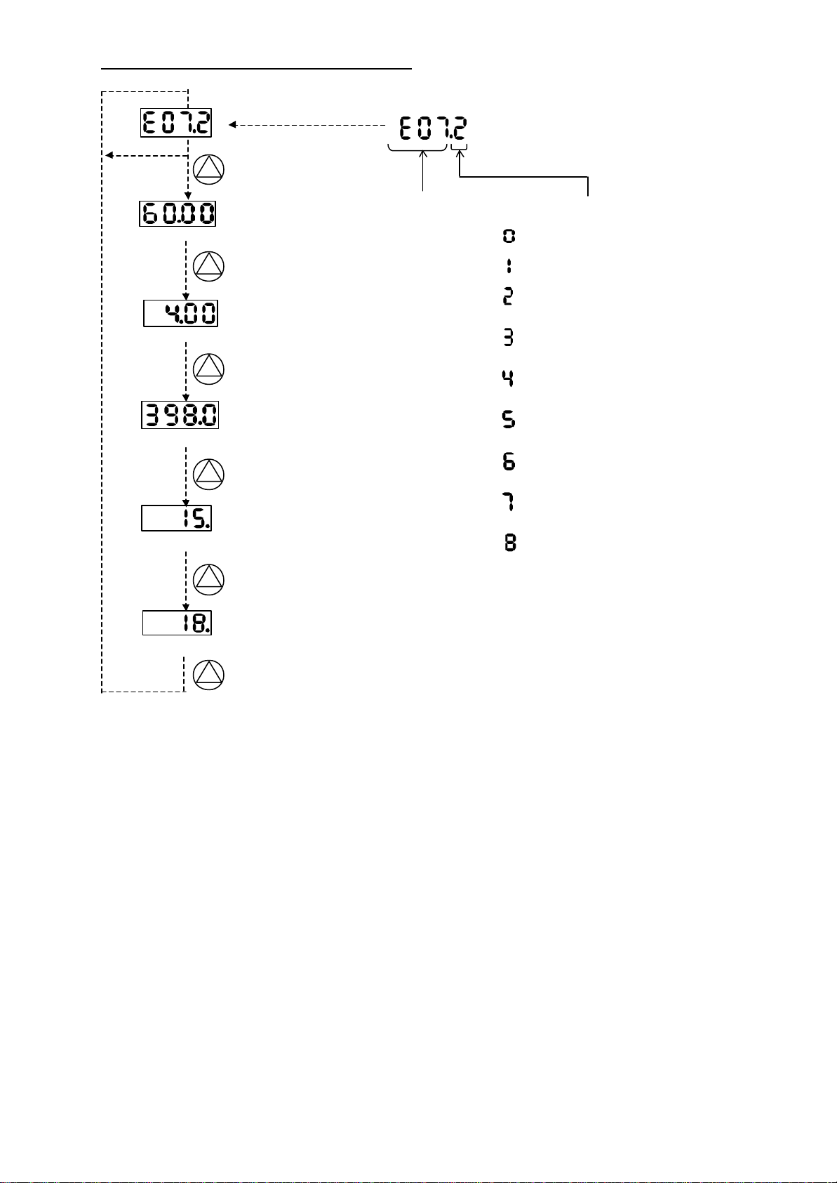
2.3 Check of the trip monitor contents
ing command ON while 0Hz command.
(1) Trip cause / Display explanation
(4) DC bus voltage at trip (V)
11111
1
(2) Output frequency at trip (Hz)
(3) Output current at trip (A)
(5) Accumulated running time until tripping (h)
Trip cause.
Refer to 4.4.1
Inverter status at tripping
: While reset
: While standstill
: While deceleration
: While constant speed
: While acceleration
: Runn
: While start procedure
: While DC injection braking
: While overload limitation
(6) Accumulated power ON time until tripping (h)
2- 4
Page 23
2.4 Check of the warning monitor contents
Warning message is come out when there is any contradiction.
Program lamp “PRG” is turned ON while warning (until the data are corrected).
Warning message and automatic rewriting
Warning Related parameters
001/ 201
002/ 202
004/ 204
005/ 205
006/ 206
009
012/ 212
015/ 215
016/ 216
021/ 221
025/ 225
031/ 231
032/ 232
035/ 235
036
037
085/ 285
086
091/ 291
092/ 292
095/ 295
096
110
120
Warning is cleared when the setting fulfils the above condition.
Date will be changed automatically to the basic code.
Frequency upper limiter A061/A261 >
Frequency lower limiter A062/A262 >
Base frequency A003/A203 >
Output frequency F001, Multistage speed 0 A020/A220 >
Multistage speed 1-15 A021-A035 >
Orientation speed setting P015 >
Frequency lower limiter A062/A262 >
Output frequency F001, Multistage speed 0 A020/A220 >
Multistage speed 1-15 A021 - A035 >
Frequency upper limiter A061/A261 <
Output frequency F001 , Multi stage speed 0 A020/A220 <
Frequency upper limiter A061/A261 <
Frequency lower limiter A062/A262 <
Output frequency F001 , Multi stage speed 0 A020/A220 <
Multi stage speed 1-15 A021-A035 <
Jogging frequency A038 <
Output frequency F001 , Multi stage speed 0 A020/A220 <>
Multi stage speed 1-15 A021-A035 <>
Frequency upper limiter A061/A261 >
Frequency lower limiter A062/A262 >
Output frequency F001 , Multi stage speed 0 A020/A220 >
Multi stage speed 1-15 A021-A035 >
Free v/f frequency 1-6 b100,b102,b104,b106,b108,b110 > Free v/f 1 b100
Free v/f frequency 2-6 b102,b104,b106,b108,b110 <
Free v/f frequency 1 b100 >
Free v/f frequency 3-6 b104,b106,b108,b110 <
Free v/f frequency 1,2 b100,b102 >
Free v/f frequency 4-6 b106,b108,b110 <
Free v/f frequency 1-3 b100,b102,b104 >
Free v/f frequency 5,6 b108,b110 <
Free v/f frequency 1-4 b100,b102,b104,b106 >
Free v/f frequency 6 b110 < Free v/f 6 b110
Free v/f frequency 1-5 b100,b102,b104,b106,b108 > Free v/f 6 b110
Free electronic thermal frequency 2,3 b017,b019 <
Free electronic thermal frequency 1 b015 >
Free electronic thermal frequency 3 b019 <
Free electronic thermal frequency 1,2 b015,b017 >
condit
ion
Base
Maximum
frequency A004/A204
Frequency upper limiter
A061/A261
Frequency lower limiter
A062/A262
Start frequency b082
Jump freq.
1/2/3 +/- Jump width
A063 +/ - A064
A065 +/- A066
A067 +/- A068 (note 1)
Free v/f 7 b112
Free v/f 1 b100
Free v/f 2 b102
Free v/f 3 b104
Free v/f 3 b104
Free v/f 4 b106
Free v/f 4 b106
Free v/f 5 b108
Free v/f 5 b108
Free electronic thermal
frequency 1 b015
Free electronic thermal
frequency 2 b017
Free electronic thermal
frequency 3 b019
(note 1)The jump frequency will be automaically re-written to the lowest jump frequency
(=jump frequency - jump width)
2- 5
Page 24

2.5 Return to an initialization setup (Factory-shipment state)
2
STR
RUN
2
STR
RUN
2
STR
RUN
The rewritten setting value is initialized and it can return to the state at the time of factory shipments.
The career of a trip is clearable.
The contents of initialization are as follows.
RUN time and power supply ON time are unclearable.
Item FNC mode Data Contents
00 Only a trip career is cleared.
Initialization
selection
b084
01
02 A clearance of a trip career and a setup are
00
Initial data
selection
b085
01 Initial cofiguration value for Europe
02 Initial cofiguration value for USA
(The initialization method)
Please initialize by the following methods after setting up the above and a setting item.
Only initialization of setting value is carried out.
Setting value will be in the state at the time of
factory shipments.
initialized.
Initial cofiguration value for inside of Japan
MIN
記憶
POWER
ALARM
Hz
V
A
%
MAX
kW
RUN
PRG
運転 停止/リセット
機能
FUNC
HITACHI
STOP/RESET
1
(1) Where a function key, a
rise key, and a down key
are pushed simultaneously,
please push stop/reset key.
If a display blinks, please
detach a stop/reset.
Then, please detach a
function key, a rise key, and
a down key.
Under initialization for Europe
HITACH
RUN
PRG
運転 停止/リセット
機能
FUNC
1
STOP/RESET
MIN
(2) Under initialization
The above-mentioned
display is for the inside
of Japan. Others are as
follows.
記憶
POWER
ALARM
Hz
V
A
%
MAX
MIN
記憶
POWER
ALARM
Hz
V
A
%
MAX
kW
HITACHI
kW
RUN
PRG
運転 停止/リセット
機能
FUNC
STOP/RESET
1
(3)When displayed on a
monitor part as "d001",
it is the completion of
initialization.
Under initialization for USA
Under trip career initialization
A display turns around a left end.
2- 6
Page 25

3.Debug Mode
Under voltage
Additional displays as follows can be seen by turning Debug mode ON (C091 ->1).
3.1 Monitor mode
No Functional Display code SJ300/L300P A Monitor or data range
1 Control frequency monitor d101 0.00-99.99/100.0-400.0Hz
2 Direct-current voltage monitor d102 0.0-999.9V
3 BRD on-monitor d103 0.00-99.99/100.0s
4 Electronic thermal monitor d104 0.00-99.99/100.0%
5 Gate array trip factor monitor d105 00-FF
6 MCU No. monitor d106 0000-9999
d101 ( Output frequency monitor (Hz)): Monitor of the output frequency of the inverter.
d102 ( DC bus voltage monitor (V)): Monitor of the DC bus voltage (VPN) of the inverter.
d103 ( BRD ON monitor (s)): There is an integrated BRD circuit on 11kW and less for SJ300, and 15kW and less
for L300P series. You can find accumulated turning ON time for the integrated BRD
transistor.
d104 ( Electronic thermal monitor (%)):You can find the usage ratio of electronic thermal performance as %.
d105 (Trip cause monitor of gate array):There are 8 items of trips which are detected by the internal gate array
and these items are transmitted to MCU.
Bit7 bit6 Bit5 bit4 bit3 bit2 bit1 bit0
Gate array
error
(E23)
Contents of d105 are expressed in HEX.
(Example 1)
20
20 (HEX) = 00100000 (BIN)
bit5 = “1” -> IGBT error (V phase)
(Example 1)
62
62 (HEX) = 01100010 (BIN)
bit1, bit5, bit6 = “1 ” -> IGBT error (U, V, W phase)
IGBT error
W phase
(E30)
IGBT error
V phase
(E30)
Over
temperature
(E21)
Over voltage
(E07)
(E09)
IGBT error
U phase
(E30)
Option
Ground fault
(E14)
d106(MCU No monitor): Display the software management number of MCU incorporated.
3- 1
Page 26

3.2 Function mode
SJ300/L300P A monitor or data range
For factory adjustment (change prohibition)
C170 to C194
JP(for Japan)/EU(for EC)/USA(for
USA)
0.2(0.2)-55.0(75.0)<75.0(90.0)-132.0>
200(200V class)/400(400V class)
Inverter (logic board) settings can be done as follows.
NO. Functional Display code
6
18 Inverter area code selection C195
19 Inverter capacity code selection C196
20 Inverter voltage class code selection C197
21 Inverter mode change selection C198 00(SJ300)/01(L300P)
Be sure to perform initialization according to the instruction manual after change the data above.
Parameter b085 is prior to C195.
change prohibition
3- 2
Page 27

3.3 A setup of an inverter
The logic board of 55 or less kW’s is common by each capacity (0.4-55kW) and the voltage class (200/400V).
Please check that name plate of logic is after SJ300P-L K.
However, it is necessary to unite with an inverter main part and to set up a logic board.
3.3.1 Setting procedure
(1) Preparation before switching on a power supply
(1)-1 Please connect a digital operator.
(2) Please carry out a power supply injection.
(3) Each code of an inverter use area, output capacity, and voltage class and model selection, and initial data is
set up.
(3)-1 It is made the debug mode.
(The setting method) Please display C091, push FUNC key, input 01 and push STR key.
(3)-2 A use area code is set up.
(The setting method) Please display C195, push FUNC key, choose either of the codes (JP, EU, USA)
shown in Table 3, and push STR key.
(3)-3 An output capacity code is set up.
(The setting method) Please push FUNC key after displaying C196. Please push a FUNC key and choose
the code SJ300 was shown in Table 1 and L300P was indicated to be to Table 2. Then,
please push STR key.
(3)-4 A voltage class code is set up.
(The setting method) Please push FUNC key after displaying C197. Please push a FUNC key and choose
the code SJ300 was shown in Table 1 and L300P was indicated to be to Table 2. Then,
please push STR key.
(3)-5 A model selection code is set up.
(The setting method) Please push FUNC key after displaying C198 . Please push a FUNC key and choose
the code indicated to be to Table 4. Then, please push STR key.
(3)-6 Data is initialized.
(The setting method) Please display b085 , push FUNC key, choose either of the codes (00, 01, 02) shown in
Table 3, and push STR key.
(4) An initial data code is set up.
(4)-1 Initialization selection is performed. (see the 2-5 clause)
(The setting method) Please display b084 , push FUNC key, input the 02 and push STR key.
Then, where a function key, a rise key, and a down key are pushed simultaneously,
please push a stop key. Please detach a stop key, if a display blinks.
Then, please detach a function key, a rise key, and a down key.
It checks whether the set-up use area code is displayed during initialization.
(for Japan : JP , for Europe : EU , for USA : USA)
(5) Please carry out power supply interception after an initialization end (after displaying d001 again).
(6) Please re-switch on a power supply.
3.3.2 Initial cofiguration completion check procedure
(1) A setup of the voltage class is checked.
(The check method) Please display A082, push FUNC key and check that it is ***.
* Please check having become as shown below about a display of the portion of ***.
Model Display
-LF/LFR -> 200
-LFU -> 230
3- 3
Model Display
-HF/HFR -> 400
-HFE -> 400
-HFU -> 460
Page 28

Code
C196
C197
H003
Code
C196
C197
H003
(2) A setup of output capacity is checked.
Model
(The check method) Please display H003, push FUNC key and check that it is ***.
* Please check having become as shown in H003 of Table 1 and Table 2 about a display of the portion of ***.
(3) Model selection of Sj300 /L300P is checked.
(The check method) Please display H-- and check that the displays when pushing FUNC key once are
SJ300:H001 and L300P:H003.
Table1.The correspondence table by the setting code model of SJ300
Code
Model
-004LF/LFU 0.4 200 0.4
-007LF/LFU 0.75 200 0.75
-015LF/LFU 1.5 200 1.5
-022LF/LFU 2.2 200 2.2
-037LF/LFU 3.7 200 3.7
-055LF/LFU 5.5 200 5.5
-075LF/LFU 7.5 200 7.5
-110LF/LFU 11.0 200 11.0
-150LF/LFU 15.0 200 15.0
-185LF/LFU 18.5 200 18.5
-220LF/LFU 22.0 200 22.0
-300LF/LFU 30.0 200 30.0
-370LF/LFU 37.0 200 37.0
-450LF/LFU 45.0 200 45.0
-550LF/LFU 55.0 200 55.0
C196
(Output
capacity)
C197
(Voltage
class)
H003
(motor
capacity)
Model
-007HF/HFE/HFU 0.75 400 0.75
-015HF/ HFE/HFU 1.5 400 1.5
-022HF HFE/HFU 2.2 400 2.2
-037HF/HFU 3.7 400 3.7
-040HFE 3.7 400 4.0
-055HF/HFE/HFU 5.5 400 5.5
-075HF/HFE/HFU 7.5 400 7.5
-110HF/HFE/HFU 11.0 400 11.0
-150HF/HFE/HFU 15.0 400 15.0
-185HF/HFE/HFU 18.5 400 18.5
-220HF/HFE/HFU 22.0 400 22.0
-300HF/HFE/HFU 30.0
-370HF/HFE/HFU 37.0 400 37.0
-450HF/HFE/HFU 45.0 400 45.0
-550HF/HFE/HFU 55.0 400 55.0
(Output
capacity)
(Voltage
class)
400 30.0
capacity)
(motor
Table2.The correspondence table by the setting code model of L300P
Code
-110LFR/LFU 11.0 200 11.0
-150LFR/LFU 15.0 200 15.0
-185LFR/LFU 18.5 200 18.5
-220LFR/LFU 22.0 200 22.0
-300LFR/LFU 30.0 200 30.0
-370LFR/LFU 37.0 200 37.0
-450LFR/LFU 45.0 200 45.0
-550LFR/LFU 55.0 200 55.0
C196
(Output
capacity)
C197
(Voltage
class)
H003
(motor
capacity)
Model
-110HFR/HFE/HFU 11.0 400 11.0
-150HFR/HFE/HFU 15.0 400 15.0
-185HFR/HFE/HFU 18.5 400 18.5
-220HFR/HFE/HFU 22.0 400 22.0
-300HFR/HFE/HFU 30.0 400 30.0
-370HFR/HFE/HFU 37.0 400 37.0
-450HFR/HFE/HFU 45.0 400 45.0
-550HFR/HFE/HFU 55.0 400 55.0
Table3.Use area code
Local selection
code
C195
(Use area)
b085
(Initial data)
For Japan JP 00
For EU EU 01
For USA USA 02
Table4. Model selection code
Model selection
code
C198
(Model selection)
SJ300 00
L300P 01
(Output
capacity)
(Voltage
class)
(motor
capacity)
3- 4
Page 29

4. The check of control power supply voltage and a control signal
3.5V
5V0VUpper arm ON
Lower arm ON
5V
0.5V
4.1 Control power supply
Item
Tolerance level
Measurement place
+ -
PV5 +5V power supply
PV12 +12V power supply
4.5V - 5.5V J1 connector 25,16pin Control terminal L
10.8V - 13.2V J1 connector 7pin Control terminal L
NV12 -12V power supply -13.2V - -10.8V J1 connector 5pin Control terminal L
PV24 24V power supply
21.6V - 26.4V
J1 connector 3,4pin,
Control terminal P24
Control terminal CM1
4.2 Control signal
Signal Measurement place The contents of operation Observation waveform
A main circuit direct-current voltage
VDC J1 connector 12pin-L
IUF
IWF
J1 connector 9pin-L
J1 connector 8pin-L
detected signal
VDC=6.396V/400V*VPN(200Vclass)
VDC=6.396V/800V*VPN(400Vclass)
A motor current detected signal
At the time of inverter rated load: About
3.3 V peak
Direct-current voltage
3.3V
-3.3V
0V
TRIP J1 connector 21pin-L
PHF J1 connector 22pin-L
IPL J1 connector 11pin-L
GS J1 connector 20pin-L
US
VS
WS
J1 connector 17pin-L
J1 connector 18pin-L
J1 connector 19pin-L
GS J1 connector 30pin-L
The signal at the time of carrying out a
trip by the trip factor which a gate array
judges (P3-1 reference)
Normal : 5V(H)
Inside of a trip : about 0.3V(L)
Phase failure protection detected
signal
Normal :5V(H)
Phase failure detection :about0.5V(L)
The instantaneous power failure signal
of R0-T0 part
Power On : about0.5V(L)
Power Off : 5V(H)
Power-module protection
Under operation : about 5V(H)
Under a stop : about 0.5V(L)
PWM signal
Upper arm ON : about 3.5V(L)
lower arm ON : about 5V(H)
The trip distinguished by GA is canceled.
Normal : about 5V(H)
Under reset : about 0.5V(L)
Direct-current voltage
Direct-current voltage
Direct-current voltage
Direct-current voltage
Reset Reset
4-1
Page 30

5. Maintenance and Inspection
5.1 Maintenance and Inspection
5.1.1 Daily inspection
Main check points to be done while operation are as follows.
(1) Whether the motor rotates as expected.
(2) Whether the installation condition have no problem.
(3) Whether there is no problem in cooling.
(4) Whether there is any abnormal vibration and noise.
(5) Whether there is any abnormal temperature rising and change in color.
(6) Whether there is any abnormal smell.
Measure the input voltage of the inverter by a tester while operation to confirm the followings.
(1) No frequent voltage fluctuation.
(2) All line voltages are balanced and stable.
5.1.2 Cleaning
Always keep the inverter clean.
Use soft cloth dipped with neutrality detergent or ethanol and wipe the dirty portion with care.
(note) Do not use such as acetone, benzene, toluene or alcohol which may damage the coating of the
inverter.
5.1.3 Periodical inspection
Check the portions where the inverter must not be in operation.
Please contact HITACHI for a periodical inspection.
(1) Is there any abnormality in cooling? ---- Cleaning of air filter.
(2) Tightening check and additional tightening. ---- Loose tightening of the screws and bolts could occur
due to vibrations and/or temperature changing. Be
sure to confirm carefully.
(3) Isn’t there any corrosion or damage in the conductors?
(4) Measurement of insulation resistance.
(5) Check and replace of cooling fan, DC bus capacitors and relays if necessary.
5- 1
Page 31

5.2 Daily and annual maintenance
Interval
D
A
Measure the voltage between
within specifications
Make short circuit R, S, T, U,
Megger test between above
Check installation for looseness.
X
X
Terminal block
X
X
Check for stuttering noise during
X
X
Check the balance of the output
voltage of each phase to phase
X
No abnormal vibration & noise?
X
Confirm the smell caused by
With and without motor
Environment
Overall
Power supply
Conductors /
Mains
Item Contents
Ambient
Devices
overall
voltage
Overall
cables
Inverter /
Converter
Check ambient temperature,
humidity, dust, corrosive gas, oil
mist, etc.
Check for abnormal vibrations
and noise.
Check voltage between
input lines
Megger check
(Power terminal - Earth)
Check for evidence of over
heating in the various
components
Cleaning X
No change in shape? X Visual inspection No abnormalities
No damage in coating?
No damage?
Tester check between each
terminal
Method Criteria
X
X Visual inspection No abnormalities
X
Remove connector J61
Disconnect power line
Remove logic terminal
X
V, W, P, PD ,N ,RB
and earth
X Visual inspection No abnormalities
Remove power cables
Measure resistance;
X
with 1ohm range
Refer to
2.1. Installation
input terminals
Tighten No abnormalities
Visual inspection No abnormalities
Visual inspection No abnormalities
Each input ⇔ P, N
Each output ⇔ P, N
Ambient temperature:
-10 ~ +50°C (no icing)
No condensation
No abnormalities and
> 5Mohm
Refer to
“5.5 How to measure
inverter &
converter“ portion
DC bus capacitor Check for leaking liquid X Visual inspection No abnormalities
Relay, contactor
Resistors
Cooling fan
Cooling
Operation check
Control circuit
Display
LED
display
Meter Working correct? X X Visual inspection Displays correct value
Overall
Motor
Insulation
resistance
Check for swelling
Check for capacitance X With capacitance meter
operation
No damage of contact?
Check for cracks or
changes in color
No open circuit? X Tester check
Check for abnormal
vibration and noise
Check for dust
without motor.
Perform a sequence protection
operation test and make sure
that there are no errors in the
protection and display circuits.
No illegible display;
No missing characters;
No segment failure of LEDs
Cleaning
No abnormal smell? X
Megger check
All terminals together - Earth
X Aural inspection No abnormalities
X Visual inspection No abnormalities
X
X
X
X Visual inspection No abnormalities
X
Visual inspection No abnormalities
Visual inspection No abnormalities
Rotate manually
during power off
Visual inspection No abnormalities
Measure the output voltage
between U, V and W
Simulate operation of the
protection circuit
Visual, aural inspection No abnormalities
overheat, damage etc.
Measure resistance;
Each input ⇔ Earth
cables
85% or more of rated
capacitance
Tolerance of within
±10% of rated value
Smooth rotation and
no abnormalities
Within 2% of voltage
difference between
each phases.
Each protection should
be performed
No abnormalities
> 5Mohm
5- 2
Page 32

5.3 Megger test
There must be no
There must be no
Disconnect all the wiring in case of megger test on external circuit, so that no test voltage is supplied to the inverter.
Use tester (high resistance range) for the test of control circuit. Do not use megger nor buzzer.
Megger test should be done only on the power (mains) portions. Do not perform megger test on control circuits.
(Use DC500V megger in case of megger test.)
In case of megger test on power terminals, disconnect short circuit material at connector “J61” located close to R0T0 terminal,
and connect R, S, T, PD, P, N, RB, U, V and W all together. Connect again the short circuit material to J61 after the test is
done.
Motor
IM
connection to the motor.
Be sure to disconnect the short circuit
material for the megger test.
Power supply
power supply
connected
DC500Vmegger
P P N R
R
S
T
Earth terminal
U
V
M
J61
5.4 Withstand voltage test
Do not perform withstand voltage test.
Semiconductors that are used in inverter can be degraded when withstand voltage is performed.
5- 3
Page 33

5.5 How to check inverter & converter portion
(Red)
(
Blk)
D4
U
W
THY
Inverter and converter module can be checked by using a tester.
(Preparation)
(1)Disconnect all the connected wires and devices to the power terminals (R, S, T, U, V, W, P and RB).
(2)Tester is to be set as 1ohm range.
(How to check)
Check the ON condition of each point shown below.
(note 1) Be sure to discharge DC bus voltage beforehand, which should be checked by DC bus voltage.
(note 2) Normally, the resistance shows ∞ in case of OFF mode.
In some cases resistance does not show ∞ due to the capacitance of DC bus capacitors.
Resistance shows 3ohm ~ 50ohm (depends on the tester voltage) in case of ON mode.
Resistance values may not be completely the same due to the electrical device (IGBT chip, diode chip…) difference.
But we can regard the result is okay if all the data are nearly the same.
Tester polarity
D1
D2
D3
D4
Converter
D5
D6
TR1
TR3
TR5
TR4
Inverter
TR6
TR2
R PD OFF
PD R ON
S PD OFF
PD S ON
T PD OFF
PD T ON
R N ON
N R OFF
S N ON
N S OFF
T N ON
N T OFF
U P OFF
P U ON
V P OFF
P V ON
W P OFF
P W ON
U N ON
N U OFF
V N ON
N V OFF
W N ON
N W OFF
RB P OFF
P RB ON
BRD
TR7
RB N OFF
N RB OFF
A K OFF
A G OFF
THY
Thyristor
K A OFF
K G ON
G A OFF
G K ON
ON; Low resistance
OFF; High resistance
Measure
ment
PD P
RB
Converter Inverter
TR1 TR3 TR5
D1
D2 D3
R
S
C+
T
D5 D6
TR7
BRD
N
TR4 TR6 TR2
Thyristor portion
A
K
G
V
5- 4
Page 34

5.6 Parts replacement
Label side of
Inverter is consists from many electrical components. And inverter cannot work properly unless all of them
works normal. Electrical components in following table are the components which may degrade according
to the usage period.
HITACHI recommend to replace those electrical components periodically to avoid any expected failure caused by them.
Parts name Recommended
period for
replacement
Cooling fan 2 ~ 3 years Replace with fresh one.
DC bus capacitors 5 years Replace with fresh one. (Decide after inspection.)
Electrolytic capacitors
on PCB
Relays - Inspection in advance
5 years Replace with fresh one. (Decide after inspection.)
(1) Cooling fan
Lifetime of the cooling fan depends on the usage condition, however it is normally around 35,000 hours.
That means it is recommended to replace the cooling fan every 2 ~ 3 years in case the inverter operates
continuously. Of course it should be replaced immediately in case the abnormality is found.
(How to remove cooling fan for mold case)
• Remove terminal cover and front cover.
‚ Reconfirm that the charge lamp is turned OFF.
ƒ Push both side of the cooling fan holder plate and pull out like following figure.
„ Remove the connector for fan connection.
Remarks
ƒ
•
(How to fix cooling fan for mold case)
• Pay attention to the direction of the cooling fan.
‚ Connect the fan connector to J21 or J22 (depends on the model) on the power PCB.
ƒ Fix the cooling fan holder board to the inverter main body.
„ Fix the front cover and terminal cover.
cooling fan
5- 5
Page 35

(How to remove cooling fan for steel case)
• Remove terminal cover and front cover.
‚ Reconfirm that the charge lamp is turned OFF.
ƒ Remove the all screws of the cooling fan case and pull out like following figure.
„ Remove the connector for fan connection.
(How to fix cooling fan for steel case)
• Pay attention to the direction of the cooling fan.
‚ Connect the fan connector to J21 or J22 or J23 or J24 (depends on the model) on the power PCB.
ƒ Fix the cooling fan case to the inverter main body.
„ Fix the front cover and terminal cover.
(2) DC bus capacitor
Big capacitance of electrolytic capacitors are used in a DC bus line of the inverter as a smoothing circuit.
Due to the chemical reaction inside the capacitor, its lifetime highly depends on the ambient temperature
and usage condition. Replacement is recommended to be done in 5 years under normal usage condition.
Also, it should be anyway replaced with new ones when there is any abnormality is found or its capacity
becomes less than 85% of its rated capacitance.
(How to remove DC bus capacitor for mold case)
• Remove terminal cover.
‚ Reconfirm that the charge lamp is turned OFF.
ƒ Remove blind cover.
„ Remove all the screws connecting capacitor PCB and power PCB.
… Pull the capacitor PCB downwards.
5- 6
Page 36

(How to fix DC bus capacitors for mold case)
• Put capacitor PCB onto the capacitor holder plate and put insulation sheet on it.
‚ Insert capacitor holder plate sliding along the ditch.
ƒ Fix the capacitor PCB with screws.
„ Fix terminal cover.
‚
(How to remove DC bus capacitor for steel case)
•
• Remove terminal cover.
‚ Under a stop confirm that the charge lamp is turned OFF.
ƒ Remove all the screws connecting P,N BAR.
„ Remove all the screws connecting capacitor case and inverter main body.
… Pull the capacitor case downwards.
(How to fix DC bus capacitors for steel case)
• Put capacitor onto the capacitor case and drive all the screws.
‚ Insert capacitor case sliding along the ditch.
ƒ Fix the capacitor case with screws.
„ Fix terminal cover.
5- 7
Page 37

5.7 Unit replacement
Unit replacement can be done without rewiring of the logic signal.
(How to exchange)
• Remove terminal cover.
‚ Reconfirm that the charge lamp is turned OFF.
ƒ Remove the screws, right and left portion , like following figure.
„ Plug out the logic terminal carefully.
… In case of plugging in to the new inverter, pay attention not to bend the connection pins.
5- 8
Page 38

No. English
1 CB circuit / DC bus capacitor circuit
2 CB board / DC bus capacitor board
3 Instantaneous power failure detection
4 Phase failure detection
5 Opt coupler / Photo coupler
6 Reference voltage
7 Inrush current limiting (circuit)
8 Thyrister drive circuit (Suppressing circuit)
9 Power supply for Thyrister gate
10 Control signal for Thyrister
11 BRD drive circuit (incl. Short circuit protection)
12 Control signal for BRD
13 Short circuit detection
14 Power supply for lower arm IGBTs
15 Drive circuit for lower arm IGBTs (incl.Short circuit detection)
16 Drive circuit for upper arm IGBTs (incl.Short circuit detection)
17 Power supply for U phase
18 Current detection for U phase
19 Current detection for W phase
20 Control power supply
21 Temperature detection
22 Control power supply
23 Power supply for GA (Gate Array)
24 Power supply for I/F (interface)
25 UV (Under voltage) detection
26 Instantaneous power failure detection
27 Dividing circuit
28 OV (Over voltage) detection
29 Voltage detection for earch phase
30 f,sita detection
31 Main PCB
32 High speed opt coupler
33 Isolation amplifier
34 30 connections between main PCB and logic PCB
35 "H" while BRD ON
36 Approx. 3.3V peak at rated current
37 "L" while Inverter trips
38 "L" while phase failure
39 Communication signal,operates while standstill
40 PWM signal
41 Approx. 6.4V at OV level
42 "L" while stopped by Gate suppressing
43 Signal for frequency matching
44 Control power supply for digital portion
45 Control power supply for analog portion
46 Power supply for I/F (interface)
47 "H" while instantaneous power failure
48 OC(Over current)detection
49 Hardware latch
50 25 control terminals
51 31 control terminals
52 Logic PCB
Page 39

Internal block diagram
Page 40

J51
1
H I T A C H I
TGToRoUVW
J1
J1
OPT1C
OPT2C
SP
SN RP SN
P24 PLC
121314
15
OOIO2
LAMAMI
AL2 AL1 AL0
Control Terminal Board
CN1
PLUG
OPEC
Plug
J61
P
Main Board
Board
G
TMN
TMP
CIB
RB
8 7 6 5 4 3 2 1
CM1
PD
R
S
SJ300-004-007LF Circuit Diagram
+ +
CTU
N
CTW
Bus Capacitor
Fin
1 2 3
J21
28 29 30
Flat Cable
FAN
1 2 3 28 29 30
OPTXC
Option Board
Digital Operator
RUN
FUNC
STOP/RESE
STR
1 2 3
1 2 3
Logic Board
58 59 60TMC
58 59 60
OPTXC
Option Board
FW FM TH
CM1 11
CM2 H
Page 41

SJ300-015 - 055LF Circuit Diagram
J51
FAN
1
H I T A C H I
PToRo
UVW
J61
J1
J1
OPT1C
OPTX
TMC
7654321
FM TH
CM1 11
12131415CM2HOOIO2
LAMAMI
AL2
AL1
ALO
J21
RSTGNGCTU
TMN
TMP
RB
PD
+
PIM
+ + +
RUN STOP/RESE
FUNC
Fin
STR
1 2 3
1 2 3
1 2 3
1 2 3
PLUG OPEC
Digital Operator
Plug
CN1
Bus Capacitor
Board
28 29 30
28 29 30
Logic Board
58 59 60
58 59 60
CTW
Main Board
Flat Cable
OPTXC
Option Board
OPT2C
Option Board
SP SN RP SN
P24 PLC
FW 8
CM1
Page 42

SJ300-075-110LF , L300P-110-150LFR Circuit Diagram
J61
FAN
1
2
H I T A C H I
PToRoUV
W
J51
J1
J1
TMC
P24 PLC
FW 8
7654321
CM1
FM TH
CM1 11
121314
15
CM2HOOIO2
LAMAMI
AL2
AL1
ALO
Digital operator
RSTGN
G
FAN
TMP
TMN
CT
Note: Control terminal symbol is SJ300.
RB
PD
PIM
+
++++++ +
FUNC
RUN
Fin
STOP/RESE
STR
1 2 3
1 2 3
Bus Capacitor
Board
1 2 3 4 5 28 29 30
1 2 3 4 5 28 29 30
PLUG OPEC
Plug
Logic Board
58 59 60
CN1
58 59 60
Flat Cable
OPT1C
OPT2C
J21
Main Board
J22
OPTXC
Option Board
OPTXC
Option Board
Control Terminal Board
SP SN RP SN
Page 43

SJ300-150 - 220LF , L300P-185 - 300LFR Circuit Diagram
J51
12H I T A C H I
PToRoUV
W
J1
J1
OPTXC
OPT2C
TMC
SP
SN RP SN
FW 8
7654321
CM1
CM1 11
12
13
14
15
CM2HO
OIO2LAMAMI
AL2
AL1
ALO
Control Terminal Board
CN1
PLUG
Digital
G
FAN
FAN
J53
J10
J11
J12
J52
J41
Control Power Board
J52
J41
PD
DM Board
J31
Thermistor
DM
G
IGBT
R
S
+
+ ++
T
N
R T
CT
J21
Main Board
J22
R
J54
J55
T
J61
OPEC
Flat Cable
OPT1C
OPTXC
Option Board
P24 PLC
RUN STOP/RESE
FUNC
STR
Operator
Plug
Logic Board
Option Board
FM TH
Note:
Control terminal symbol is SJ300.
J10 is installed only for SJ300-150LF
and L300P-185LFR.
Page 44

1
H I T A C H I
OPTXC
OPT2C
TMC
SP SN RP SN
FW 8
7654321
CM1
FM TH
CM1 11
121314
15
CM2
HOOIO2L
AM
AMI
AL2
AL1
ALO
CN1
PLUG
OPEC
Digital
SJ300-300LF, L300P-370LFR Circuit Diagram
FAN
UVW
J1
FAN
J11
J16
J52
J41
J52
J41
FAN
J71
J71
J56
J56
J53
Control
J51
To
Ro
J65
J65
J1
PRSTGNG
PD
Power
Board
J62
J62
DM Board
R
R
T
J64
J64
J54
J55
J31
J32
DM
Thermistor
Thermistor
IGBT
CTU
+
+ + +
CTW
T
CT Board
J21
Main Board
J22
Flat Cable
J23
OPT1C
OPTXC
J61
Pre Control Power Board
P24 PLC
FUNC
RUN
STOP/RESE
STR
Operator
Plug
Option Board
Logic Board
Option Board
Control Terminal Board
Note: Control terminal symbol is SJ300.
Page 45

2
H I T A C H I
OPTXC
OPTXC
OPT2C
TMC
SP SN RP SN
7654321
CM1
FM TH
CM1 11
121314
15
CM2HO
OIO2L
AM
AMI
AL2
AL1
ALO
CN1
PLUG
Digital
SJ300-370-450LF, L300P-450-550LFR Circuit Diagram
J1
J11
J16
J52
J41
J52
J41
J71
J71
J56
J56
J53
Control Power
J51
To
Ro
Pre Control
J65
J65
J1
FAN
FAN
FAN
FAN
PRSTG
N
J10
PD
G
Board
J62
J62
DM Board
R T
R
T
J64
J64
J54
J55
DM
THY
+
+ + +
IGBT
Main board
Flat Cable
CTU
CTW
CT Board
OPT1C
J31
J32
J33
J21
J22
J23
J24
Thermistor
Thermistor
Thermistor
U
V
W
J61
Power Board
P24 PLC
FW 8
FUNC
RUN
1
STOP/RESE
STR
Operator
Plug
OPEC
Option Board
Logic Board
Option Board
Control Terminal Board
Note: Control terminal symbol is SJ300.
Page 46

Note: Control terminal symbol is SJ300.
2
H I T A C H I
OPTXC
OPT2C
TMC
SP SN RP SN
FW 8
7654321
CM1
FM TH
CM1 11
121314
15
CM2
HOOIO2L
AM
AMI
AL2
AL1
ALO
CN1
PLUG
Digital
SJ300-550LF,L300P-750LFR Circuit Diagram
J1
TUG
J52
J41
Flat Cable
J52
J41
FAN
FAN
FAN
J71
J71
J56
CT Board
J53
Control
J51ToRo
Pre Control
J65
J65
J1
TUE
TXG
TXE
RSTGN
GPDP
J10
J31
Thermistor
DM Board
Power Board
J62
J62
R
T
R T
J54
J55
J64
J64
DM
THY
+
+ + +
IGBT
Snubber Module
Main Board
R1-R6
CTU
CTW
J32
J33
J21
J22
J23
Thermistor
Thermistor
U
V
W
OPTXCOPT1C
J61
Power Board
P24 PLC
FUNC
RUN
1
STOP/RESE
STR
Operator
Plug
OPEC
Option Board
Logic Board
Option Board
Control Terminal Board
Page 47

H I T A C H I
P
RB
RST
G
J51
ToRoUVWNJ61
OPTXC
OPT2C
SP
SN RP SN
P24 PLC
CM1 11
121314
15
HOOIO2LAMAM
AL
AL1
AL0
Control Terminal Board
PLUG
OPEC
Digital Operator
J1
J1
Bus Capacitor
G
CTU
CTW
TM
TM
CIB
1
2
PD
SJ300-007HF Circuit Diagram
+
+
RU
PR
FUNC
RUN
Fin
STOP/RESE
STR
1 2 3
1 2 3
FW 8 7 6 5 4 3 2 1 CM1 FM TH
POWE
ALAR
H
Board
1 2 3 28 29 30
1 2 3
Plug
28 29 30
Logic Board
58 59 60TMC
CN1
58 59 60
CM2
Main Board
Flat Cable
OPT1C
Option Board
OPTXC
Option Board
J21
FAN
Page 48

J51
FAN
1
H I T A C H I
RUN
PToRoUVWJ61
OPTXC
OPT2C
SP
SN RP SN
P24 PLC
7654321
FM TH
CM1 11
12
131415
CM2
HOOI
O2
AL2
AL1
ALO
Control Terminal Board
PLUG
OPEC
Digital Operator
J1
J1
RSTGN
CTU
CTW
TMN
TMP
PIM
PD
RB
G
SJ300-015-055HF Circuit Diagram
+
+++
Bus Capacitor
Board
FUNC
1 2 3 4 5 28 29 30
Fin
1 2 3 4 5
STOP/RESE
Plug
STR
1 2 3 4 5
1 2 3 4 5
FW 8
CN1
CM1
28 29 30
Logic Board
55 56 57 58 59 60TMC
55 56 57 58 59 60
Min Board
Flat cable
OPT1C
J21
Option Board
OPTXC
Option Board
L AM AMI
Page 49

FAN
1
2
P
J51ToRo
UVW
J61
J1
J1
Option Board
OPTXC
OPT1C
OPTXC
OPT2C
SP
SN RP SN
P24 PLC
FW 8
7654321
FM TH
121314
15
CM2
OIO2LAMAMI
AL2ALALO
Control Terminal Board
RSTGN
+
+
TMP
TMN
FAN
PIM
PD
RB
SJ300-075-110HF , L300P-110-150HFR Circuit Diagram
+
+
++++
Bus Capacitor
G
Board
Main Board
CT
J21
J22
1 2 3 28 29 30
Fin
H I T A C H I
1 2 3
28 29 30
Flat Cable
PLUG OPEC
FUNC
RUN
STOP/RESE
STR
1 2 3
Digital operator
Plug
Logic Board
58 59 60TMC
Option Board
1 2 3
CN1
CM1
CM1 11
58 59 60
H O
Note: Control terminal symbol is SJ300.
Page 50

SJ300-150 - 220HF , L300P-185 - 300HFR Circuit Diagram
J51
12H I T A C H I
PToRo
J1
J1
OPT1C
OPTXC
OPT2C
TMC
SP
SN RP SN
FW 8
7654321
CM1
FM TH
121314
15
CM2
HOOIO2LAMAMI
AL2
AL1
ALO
CN1
PLUG
Digital
T
G
J53
J10
J11
J12
J52
J41
Control Power
Board
J52
J41
VWU
FAN
FAN
PD
G
R
S
N
DM Board
R
J54
J55
R T
T
DM
J61
+
OPEC
J31
Thermistor
IGBT
+
++
CT
J21
Main Board
J22
Flat Cable
OPTXC
Option Board
P24 PLC
FUNC
RUN
STOP/RESE
STR
Operator
Plug
Logic Board
Option Board
Control Terminal Board
CM1 11
Note: Control terminal symbol is SJ300
Page 51

SJ300- 300HF , L300P-370HFR Circuit Diagram
12H I T A C H I
PUV
W
J1J1OPTXC
OPTXC
OPT2C
TMC
SP
SN RP SN
FW 8
7654321
CM1 FM TH
CM1 11
121314
15
CM2HO
OIO2LAMAMI
AL2
AL1
ALO
Control Terminal Board
CN1
PLUG
Digital
T
GNG
CTW
J10
J11
J16
J52
J41
J52
J41
Note: Control terminal symbol is SJ300
J53
Control
J51
To
Ro
Pre Control Power Board
J65
J65
FAN
FAN
FAN
J71
J71
J56
J56
PD
R
S
DM Board
Power Board
J62
J62
R
T
J64
J64
R T
J54
J55
DM
J31
J32
Thermistor
Thermistor
IGBT
+
+
CTU
++
CT Board
J21
Main Board
J22
J23
OPT1C
J61
P24 PLC
FUNC
RUN
STOP/RESE
STR
Operator
Plug
OPEC
Option Board
Logic Board
Option Board
Page 52

SJ300-370- 550HF,L300P-450-750HFR Circuit Diagram
1
2
H I T A C H I
PRS
TGUVW
J1
J1
OPTXC
OPT2C
TMC
SP SN RP SN
FW 8
7654321
CM1
FM TH
CM1 11
121314
15
CM2
HOOIO2L
AM
AMI
AL2
AL1
ALO
CN1
PLUG
Digital
G
J11
J16
J52
J41
J52
J41
J53
Control
J51
To
Ro
Pre Control
J65
J65
J71
J71
J56
J56
FAN
FAN
FAN
FAN
J10
PD
N
DM Board
Power Board
J62
J62
R
T
J64
J64
R T
J54
J55
DM
J31
J32
J33
Thermistor
Thermistor
Thermistor
IGBT
+
+
CTU
++
CTW
CT Board
J21
Main board
J22
J23
Flat Cable
J24
OPT1C
OPTXC
J61
Power Board
P24 PLC
FUNC
RUN
STOP/RESE
STR
Operator
Plug
OPEC
Option Board
Logic Board
Option Board
Control Terminal Board
Note: Control terminal symbol is SJ300.
Page 53

2
OPTXC
OPT1C
OPT2C
TMC
654321CM1
121314
15
HOOIO2L
CN1
Digital
SJ300-750-1320HF , L300P-900-1320HFR Circuit Diagram
UVWJ1PRSTGNG
J52
J41
J52
J41
J53
Control
J51ToRo
Pre Control
J65
J65
J1
FAN
JU1
J80
JU2
JX1
JX2
FAN
FAN
GEG
E
PD
J31
Thermistor
J21
J22
J23
DM Board
Power Board
J62
J62
R
T
J64
J64
R T
J54
J55
DM
H I T A C H I
J10
THY R1-R6
+ + + +
+ + ++
Driver Board
(Total 6)
IGBT
Main Board
PLUG
OPEC
CTU
CTW
GA Board
Flat Cable
J35
Thermistor
Option Board
J61
Power Board
SP SN RP SN
P24 PLC
FW 8
7
FUNC
RUN
1
STOP/RESE
STR
Operator
Plug
FM TH
CM1 11
Logic Board
CM2
OPTXC
Option Board
AMI AL2 AL1
AM
Note : Control terminal symbol is SJ300
Only SJ300-1100,1320HF and
ALO
L300P-1320HFR Connect FAN to J23
Page 54

Page 55

Page 56

Page 57

Page 58

Page 59

Page 60

Page 61

Page 62

Page 63

Page 64

Page 65

Page 66

Page 67

Page 68

Page 69

Page 70

Page 71

Page 72

SJ300/L300P Series SPARE PARTS LIST
No. Parts No. Drawing No. Description Remarks Applied Model Qty/Unit No. Parts No. Drawing No. Description Remarks Applied Model Qty/Unit
255023 3T017245-1
1
255024 3T017245-2
1
255025 3T017245-3
1
255026 3T017997-1
1
255027 3T017997-2
1
255028 3T017997-3
1
255029 3T017997-4
1
255030 3T017997-6
1
254065 3T017997-10
1
254066 3T017997-11
1
254068 3T017997-8
1
254069 3T017997-9
1
255067 3T011307-2
8
255063 3T016823-1
8
255062 3T011307-8
8
255064 3T016823-4
8
255065 3T018306-1
8
255066 3T018716-1
8
255042 NCM150TU1-2F IGBT Module 150A/600V
13
255043 NCM200TU1-2F IGBT Module 200A/600V
13
255044 N2MBI300S-06 IGBT Module 300A/600V
13
255045 NCM300DU1-2F IGBT Module 300A/600V
13
255046 NCM400DU1-2F IGBT Module 400A/600V
13
255047 NCM600HU1-2F IGBT Module 600A/600V
13
255048 NCM75TU24- F IGBT Module 75A/1200V
13
255049 NCM100TU24- F IGBT Module 100A/1200V
13
255050 N2MBI150C-12 IGBT Module 150A/1200V
13
255051 NCM150DU2-4F IGBT Module 150A/1200V
13
DC Bus Capacitor 1500uF 150LFU,LFE,HFU,HFE 185LFU,LFE,HFU,HFE 4
DC Bus Capacitor 1800uF 185LFU,LFE,HFU,HFE 220LFU,LFE,HFU,HFE 4
DC Bus Capacitor 2200uF 220LFU,LFE,HFU,HFE 300LFU,LFE,HFU,HFE 4
DC Bus Capacitor 3300uF 300LFU,LFE,HFU,HFE 370LFU,LFE,HFU,HFE 4
DC Bus Capacitor 3900uF 370LFU,LFE,HFU,HFE 450LFU,LFE,HFU,HFE 4
DC Bus Capacitor 4700uF 450LFU,LFE,HFU,HFE 550LFU,LFE,HFU,HFE 4
DC Bus Capacitor 5600uF 550HFU,HFE 750HFU,HFE 4
DC Bus Capacitor 5600uF 550LFU,LFE 750LFU 4
DC Bus Capacitor 3300uF 750HFU,HFE 900HFU,HFE 8
DC Bus Capacitor 3900uF 900HFU,HFE 1100HFU,HFE 8
DC Bus Capacitor 4700uF 1100HFU,HFE 1320HFU,HFE 8
DC Bus Capacitor 5600uF 1320HFU,HFE 8
Main Circuit Terminals M6 150,185LFU,LFE
Main Circuit Terminals M8 220LFU,LFE 220,300LFU,LFE 1
Main Circuit Terminals M6 300,370HFU,HFE 370HFU,HFE 1
Main Circuit Terminals M8 300,370LFU,LFE,
Main Circuit Terminals M10 450LFU,LFE
Main Circuit Terminals M10 550LFU,LFE
SJ300 L300P SJ300 L300P
150-220HFU,HFE
450,550HFU,HFE
750,900HFU,HFE
1100,1320HFU,HFE
150,185LFU,LFE 185,220LFU,LFE
220LFU,LFE 300LFU,LFE
300LFU,LFE 370LFU,LFE
370LFU,LFE 450LFU,LFE
450LFU,LFE 550LFU,LFE
550LFU,LFE 750LFU
150-185HFU,HFE 185-220HFU,HFE
220HFU,HFE 300HFU,HFE
300HFU,HFE 370HFU,HFE
370HFU,HFE 450HFU,HFE
185LFU,LFE
185-300HFU,HFE
370LFU,LFE
450-750HFU,HFE
450-750LFU,LFE
900,1100HFU,HFE
1320HFU,HFE 1
255052 NCM200DU2-4F IGBT Module 200A/1200V
13
255053 NCM300DU2-4F IGBT Module 300A/1200V
13
254070 NMBN400GR-12 IGBT Module 400A/1200V
13
254071 NMBN600GR-12 IGBT Module 600A/1200V
13
255040 NPHT2508 Thyristor Module 250A/800V
14
255041 NPHT4008 Thyristor Module 400A/800V
14
254077 NPHT25016 Thyristor Module 250A/1600V
14
255177 NPHT40016 Thyristor Module 400A/1600V
14
255031 NPGH1008A- M Diode Module 100A/800V
15
255033 NPGH1508A- M Diode Module 150A/800V
15
255036 NPGH2008A-M Diode Module 200A/800V
15
255038 NPD1008AC Diode Module 100A/800V
15
1
1
1
1
1
3
3
3
6
1
1
3
3
255039 NPD1508 Diode Module 150A/800V
15
255032 NPGH5016A-M Diode Module 50A/1600V
15
255034 NPGH7516A-M Diode Module 75A/1600V
15
255035 NPGH10016-AM Diode Module 100A/1600V
15
255037 NPGH20016-AM Diode Module 200A/1600V
15
254084 NPD10016 Diode Module 100A/1600V
15
254086 NPD15116 Diode Module 150A/1600V
15
254099 2T004540-1 Front Cover
19-2
254101 2T004549-1 Front Cover
19-2
254103 2T004568-1 Front Cover
19-2
254230 2T004549-2 Front Cover
19-2
254251 2T004568-2 Front Cover
19-2
254103 2T004568-1 Front Cover
19-2
254230 2T004549-2 Front Cover
19-2
254251 2T004568-2 Front Cover
19-2
254373 4T016893-1A Terminals Cover
19-3
450HFU,HFE 550HFU,HFE
550HFU,HFE 750HFU,HFE
750,900HFU,HFE 900,1320HFU,HFE
1100,1320HFU,HFE 1320HFU,HFE
370,450LFU,LFE 450,550LFU,LFE
550LFU,LFE 750LFU
750,900HFU,HFE 900,1100HFU,HFE
1100,1320HFU,HFE 1320HFU,HFE
150LFU,LFE 185LFU,LFE
185,220LFU,LFE 220LFU,LFE
300LFU,LFE 300,370LFU,LFE
370,450LFU,LFE 450,550LFU,LFE
550LFU,LFE 750LFU
150HFU,HFE 185HFU,LFE
185,220HFU,HFE 220,300HFU,HFE
300HFU,HFE 370HFU,HFE
370,450,550HFU,HFE 450,550,750HFU,HFE
750,900HFU,HFE 900,1100HFU,HFE
1100,1320HFU,HFE 1320HFU,HFE
004-055LFU,LFE
007-055HFU,HFE
075-110LFU,LFE
075-110HFU,HFE
150-220LFU,LFE
150-220HFU,HFE
150-220LFU,LFE
150-220HFU,HFE
004-055LFU,LFE
007-055HFU,HFE
110-150LFU,LFE
110-150HFU,HFE
185-300LFU,LFE
185-300HFU,HFE
110-150LFU,LFE
110-150HFU,HFE
185-300LFU,LFE
185-300HFU,HFE
3
3
6
6
1
1
1
1
1
1
1
3
3
1
1
1
1
3
3
1
1
1
1
1
1
1
1
1
Page 73

SJ300/L300P Series SPARE PARTS LIST
No. Parts No. Drawing No. Description Remarks Applied Model Qty/Unit No. Parts No. Drawing No. Description Remarks Applied Model Qty/Unit
254501 4T016894-1A Terminals Cover
19-3
254502 4T016895-1A Terminals Cover
19-3
254503 4T016894-1B Terminals Cover
19-3
254504 4T016895-1B Terminals Cover
19-3
254814 3T016788-1 Spacer Cover
19-5
254815 3T016788-2 Spacer Cover
19-5
254979 3T016596-1 Cooling Fan Attachment Board
19-6
254980 2T004544-1 Cooling Fan Attachment Board
19-6
254986 2T004566-1 Cooling Fan Attachment Board
19-6
254990 2T004544-2 Cooling Fan Attachment Board
19-6
254991 2T004566-2 Cooling Fan Attachment Board
19-6
254992 3T016597-3 DC Bus Capacitor Attachment
19-7
255006 3T016597-1 DC Bus Capacitor Attachment
19-7
255119 2T004545-1 DC Bus Capacitor Attachment
19-7
255122 2T004565-1 DC Bus Capacitor Attachment
19-7
255123 2T004545-2 DC Bus Capacitor Attachment
19-7
255124 2T004565-2 DC Bus Capacitor Attachment
19-7
254808 1T001890-1 Main Body Cover
19-11
254810 1T001894-1 Main Body Cover
19-11
254811 1T001906-1 Main Body Cover
19-11
254812 1T001894-2 Main Body Cover
19-11
254813 1T001906-2 Main Body Cover
19-11
255020 3T016890-1 Cooling Fan
21
255021 3T016989-1 Cooling Fan
21
255021 3T016989-1 Cooling Fan
21
255021 3T016989-1 Cooling Fan
21
255022 3T018969-1 Cooling Fan
21
254515 3T019914-1 Cooling Fan
21
Block
Block
Block
Block
Block
Block
(MMF-06F24ES-RN1)
(MMF-08D24ES-RN2)
(MMF-08D24ES-RN2)
(MMF-08D24ES-RN2)
(MMF-12D24DS-RN5)
(109P1324S103)
SJ300 L300P SJ300 L300P
075-110LFU,LFE
075-110HFU,HFE
150-220LFU,LFE
150-220HFU,HFE
004-550LFU,LFE
007-1320HFU,HFE
004-055LFU,LFE
007-055HFU,HFE
075-110LFU,LFE
075-110HFU,HFE
150-220LFU,LFE
150-220HFU,HFE
004-007LFU,LFE
007HFU,HFE
015-055LFU,LFE
015-055HFU,HFE
075-110LFU,LFE 075110HFU,HFE
150-220LFU,LFE
150-220HFU,HFE
004-055LFU,LFE
007-055HFU,HFE
075-110LFU,LFE 075110HFU,HFE
150-220LFU,LFE 150220HFU,HFE
60mm DC24V 004-055LFU,LFE
007-055HFU,HFE
80mm DC24V 075-220LFU,LFE,HFU,HFE 110-300LFU,LFE,HFU,HFE
80mm DC24V 300LFU,LFE,HFU,HFE 370LFU,LFE,HFU,HFE
80mm DC24V 370,450LFU,LFE
120mm DC24V 550LFU,LFE 750LFU
127mm DC24V 750,900HFU,HFE 900,1100HFU,HFE
370-550HFU,HFE
110-150LFU,LFE
110-150HFU,HFE
185-300LFU,LFE
185-300HFU,HFE
110-750LFU,LFE
110-1320HFU,HFE
110-150LFU,LFE 110150HFU,HFE
185-300LFU,LFE
185-300HFU,HFE
110-150LFU,LFE
110-150HFU,HFE
185-300LFU,LFE
185-300HFU,HFE
110-150LFU,LFE
110-150HFU,HFE
185-300LFU,LFE 185300HFU,HFE
450,550LFU,LFE,HFU,HFE
750HFU,HFE
1
1
1
1
1
1
1
1
1
1
1
1
1
1
1
1
1
1
1
1
1
1
1
2
3
4
3
2
254515 3T019914-1 Cooling Fan
21
254516 SJ3 CB004L DC Bus capacitor PCB
60
254517 SJ3 CB007L DC Bus capacitor PCB
60
255008 SJ3 CB015L DC Bus capacitor PCB
60
255009 SJ3 CB022L DC Bus capacitor PCB
60
255010 SJ3 CB037L DC Bus capacitor PCB
60
255011 SJ3 CB055L DC Bus capacitor PCB
60
255016 SJ3 CB075L DC Bus capacitor PCB
60
255017 SJ3 CB110L DC Bus capacitor PCB
60
254518 SJ3 CB007H DC Bus capacitor PCB
60
255012 SJ3 CB015H DC Bus capacitor PCB
60
255013 SJ3 CB022H DC Bus capacitor PCB
60
255014 SJ3 CB037H DC Bus capacitor PCB
60
255015 SJ3 CB055H DC Bus capacitor PCB
60
255018 SJ3 CB075H DC Bus capacitor PCB
60
255019 SJ3 CB110H DC Bus capacitor PCB
60
254937 SJ300P-L Logic PCB
61
255146 SJ300P-L Logic PCB
61
254049 SJ300TM Control circuit Terminals PCB
62
255007 L300PTM Control circuit Terminals PCB
62
254040 SJ3 D030-55L ROTO PCB
63
254043 SJ3 D030-55H ROTO PCB
63
254519 SJ3 B007L Main PCB with Main body case
64
254520 SJ3 B004L Main PCB with Main body case
64
255099 SJ3 B015L Main PCB with Main body case
64
255100 SJ3 B022L Main PCB with Main body case
64
255101 SJ3 B037L Main PCB with Main body case
64
255102 SJ3 B055L Main PCB with Main body case
64
(109P1324S103)
127mm DC24V 1100,1320HFU,HFE 1320HFU,HFE
004LFU,LFE
007LFU,LFE
015LFU,LFE
022LFU,LFE
037LFU,LFE
055LFU,LFE
075LFU,LFE 110LFU,LFE
110LFU,LFE 150LFU,LFE
007HFU,HFE
015HFU,HFE
022HFU,HFE
037HFU,HFE
055HFU,HFE
075HFU,HFE 110HFU,HFE
110HFU,HFE 150HFU,HFE
004-550LFU,LFE
007-550HFU,HFE
750-1320HFU,HFE 900-1320HFU,HFE
004-550LFU,LFE
007-1320HFU,HFE
110-750LFU,LFE
300-550LFU,LFE 370-750LFU,LFE
300-1320HFU,HFE 370-1320HFU,HFE
004LFU,LFE
007LFU,LFE
015LFU,LFE
022LFU,LFE
037LFU,LFE
055LFU,LFE
110-750LFU,LFE
110-750HFU,HFE
110-1320HFU,HFE
3
1
1
1
1
1
1
1
1
1
1
1
1
1
1
1
1
1
1
1
1
1
1
1
1
1
1
1
Page 74

SJ300/L300P Series SPARE PARTS LIST
No. Parts No. Drawing No. Description Remarks Applied Model Qty/Unit No. Parts No. Drawing No. Description Remarks Applied Model Qty/Unit
254985 SJ3 B075L Main PCB with Main body case
64
255103 SJ3 B110L Main PCB with Main body case
64
255104 SJ3 B150L Main PCB
64
255105 SJ3 B185L Main PCB
64
255106 SJ3 B220L Main PCB
64
255110 SJ3 B300L Main PCB
64
255098 SJ3 B370L Main PCB
64
255112 SJ3 B450L Main PCB
64
255116 SJ3 B550L Main PCB
64
254521 SJ3 B007H Main PCB with Main body case
64
254981 SJ3 B015H Main PCB with Main body case
64
254982 SJ3 B022H Main PCB with Main body case
64
254983 SJ3 B037H Main PCB with Main body case
64
254984 SJ3 B055H Main PCB with Main body case
64
254987 SJ3 B075H Main PCB with Main body case
64
254988 SJ3 B110H Main PCB with Main body case
64
255107 SJ3 B150H Main PCB
64
255108 SJ3 B185H Main PCB
64
255109 SJ3 B220H Main PCB
64
255111 SJ3 B300H Main PCB
64
255113 SJ3 B370H Main PCB
64
255114 SJ3 B450H Main PCB
64
255115 SJ3 B550H Main PCB
64
254522 SJ3 B750H Main PCB
64
254523 SJ3 B900H Main PCB
64
254524 SJ3 B1100H Main PCB
64
254525 SJ3 B1320H Main PCB
64
254526 L3P B900H Main PCB
64
SJ300 L300P SJ300 L300P
075LFU,LFE
110FU,LFE
150LFU,LFE
185LFU,LFE
220LFU,LFE
300LFU,LFE 370LFU,LFE
370LFU,LFE 450LFU,LFE
450LFU,LFE 550LFU,LFE
550LFU,LFE 750LFU
007HFU,HFE
015HFU,HFE
022HFU,HFE
037HFU,HFE
055HFU,HFE
075HFU,HFE
110HFU,HFE
150HFU,HFE
185HFU,HFE
220HFU,HFE
300HFU,HFE 370HFU,HFE
370HFU,HFE 450HFU,HFE
450HFU,HFE 550HFU,HFE
550HFU,HFE 750HFU,HFE
750HFU,HFE
900HFU,HFE
1100HFU,HFE
1320HFU,HFE
900HFU,HFE
1
1
1
1
1
1
1
1
1
1
1
1
1
1
1
1
1
1
1
1
1
1
1
1
1
1
1
1
254527 L3P 1100H Main PCB
64
254528 L3P 1320H Main PCB
64
255117 L3P B110L Main PCB with Main body case
64
255118 L3P B150L Main PCB with Main body case
64
254995 L3P B185L Main PCB
64
254996 L3P B220L Main PCB
64
254997 L3P B300L Main PCB
64
254993 L3P B110H Main PCB with Main body case
64
254994 L3P B150H Main PCB with Main body case
64
254998 L3P B185H Main PCB
64
254999 L3P B220H Main PCB
64
255000 L3P B300H Main PCB
64
255054 SJ3 S300L CT/Snubber PCB
65
255056 SJ3 S370L CT/Snubber PCB
65
255057 SJ3 S450L CT/Snubber PCB
65
255058 SJ3 CT550L CT PCB
65
255055 SJ3 S300H CT/Snubber PCB
65
255059 SJ3 S370H CT/Snubber PCB
65
255060 SJ3 S450H CT/Snubber PCB
65
255061 SJ3 S550H CT/Snubber PCB
65
254529 L3P S370L CT/Snubber PCB
65
254530 L3P S450L CT/Snubber PCB
65
254534 L3P S550L CT/Snubber PCB
65
254536 L3P CT750L CT PCB
65
254531 L3P S370H CT/Snubber PCB
65
254532 L3P S450H CT/Snubber PCB
65
254533 L3P S550H CT/Snubber PCB
65
254535 L3P S750H CT/Snubber PCB
65
300LFU,LFE
370LFU,LFE
450LFU,LFE
550LFU,LFE
300HFU,HFE
370HFU,HFE
450HFU,HFE
550HFU,HFE
1100HFU,HFE
1320HFU,HFE
110LFU,LFE
150LFU,LFE
185LFU,LFE
220LFU,LFE
300LFU,LFE
110HFU,HFE
150HFU,HFE
185HFU,HFE
220HFU,HFE
300HFU,HFE
370LFU,LFE
450LFU,LFE
550LFU,LFE
750LFU
370HFU,HFE
450HFU,HFE
550HFU,HFE
750HFU,HFE
1
1
1
1
1
1
1
1
1
1
1
1
1
1
1
1
1
1
1
1
1
1
1
1
1
1
1
1
Page 75

SJ300/L300P Series SPARE PARTS LIST
No. Parts No. Drawing No. Description Remarks Applied Model Qty/Unit No. Parts No. Drawing No. Description Remarks Applied Model Qty/Unit
255084 SJ3 C15L DM PCB
66
255085 SJ3 C18-30L DM PCB
66
255086 SJ3 C37-45L DM PCB
66
255087 SJ3 C55-90L DM PCB
66
255088 SJ3 C15-30H DM PCB
66
255089 SJ3 C37-55H DM PCB
66
254537 SJ3 C75-90H DM PCB
66
254538 SJ3 CX1-X6H DM PCB
66
255001 SJ3D15-22L Power Source PCB
67
255003 SJ3D30-45L Power Source PCB
67
255005 SJ3D55-75L Power Source PCB
67
255002 SJ3D15-22H Power Source PCB
67
255004 SJ3D30-55H Power Source PCB
67
254539 SJ3 D75-X3H Power Source PCB
67
OPE-S OPE-S Digital Operator
68
OPE-SR OPE-SR Digital Operator
68
OPE-SR OPE-SR(E) Digital Operator
68
254431 N4W563JB Blance Resistor
69
254431 N4W563JB Blance Resistor
69
254432 N4W563JB6 Blance Resistor
69
254432 N4W563JB6 Blance Resistor
69
254432 N4W563JB6 Blance Resistor
69
255074 4T015352-1 Snubber Capacitor
70
255075 4T015352-3 Snubber Capacitor
70
255080 3T018884-1 Snubber Capacitor
70
255147 4T016028-1 Snubber Capacitor
70
255148 4T016028-2 Snubber Capacitor
70
255149 4T016028-3 Snubber Capacitor
70
Cable Length
100mm
Cable Length
310mm 250mm
Cable Length
400mm 300mm
Cable Length
480mm 390mm
SJ300 L300P SJ300 L300P
150LFU,LFE 185LFU,LFE
185-300LFU,LFE 220-370LFU,LFE
370-450LFU,LFE 450-550LFU,LFE
550LFU,LFE 750LFU
150-300HFU,HFE 185-370HFU,HFE
370-550HFU,HFE 450-750HFU,HFE
750,900HFU,HFE 900,1100HFU,HFE
1100,1320HFU,HFE 1320HFU,HFE
150-220LFU,LFE 185-300LFU,LFE
300-450LFU,LFE 370-550LFU,LFE
550LFU,LFE 750LFU
150,220HFU,HFE 185-300HFU,HFE
300-550HFU,HFE 370-750HFU,HFE
750-1320HFU,HFE 900-1320HFU,HFE
All models for EC-version 1
All models for EC-version 1
All models for US-version All models for US-version 1
150-220LFU,LFE,HFU,HFE 185-300LFU,LFE,HFU,HFE
750,900HFU,HFE 900,1100HFU,HFE
300-550LFU,LFE 370-750LFU,LFE
300-550HFU,HFE 370-750HFU,HFE
1100,1320HFU,HFE 1320HFU,HFE
150-220LFU,LFE 185-300LFU,LFE
150-220HFU,HFE 185-300HFU,HFE
550LFU,LFE 750LFU
550HFU,HFE 750HFU,HFE
550HFU,HFE 750HFU,HFE
550HFU,HFE 750HFU,HFE
1
1
1
1
1
1
1
1
1
1
1
1
1
1
4
8
2
4
8
1
1
3
1
1
255081 3T018886-1 Snubber Capacitor
71
255076 4T016022-1 Snubber Capacitor Non cable
72
255077 4T016093-1 Snubber Capacitor
73
255078 4T016093-2 Snubber Capacitor
73
255079 4T016093-3 Snubber Capacitor
73
255082 4T014614- 1 FFC
75
255083 4T014614- 2 FFC
75
255072 N55029881-0 Digital Operetor Connection Plug
76
253006 3T001303-16 Snubber Resistor
79
253006 3T001303-16 Snubber Resistor
79
255068 4T014572-3 Current Limiting Resistor
80
255070 3T011643-3 Current Limiting Resistor
80
255069 4T014572-3 Current Limiting Resistor
80
255071 3T011643-4 Current Limiting Resistor
80
254540 3T013573-17 Current Limiting Resistor
80
254541 3T013573-18 Current Limiting Resistor
80
254805 3T016852-2 Wiring Blind Cover
81
254806 3T016959-2 Wiring Blind Cover
81
254807 3T017422-2 Wiring Blind Cover
81
254795 4T016519-1 Thermistor
86
254796 4T016519-1 Thermistor
86
254797 4T016519-3 Thermistor
86
254796 4T016519-2 Thermistor
86
254796 4T016519-2 Thermistor
86
254798 SJ3 DR75-90H Driver PCB
95
254799 SJ3 DRX1-X3H Driver PCB
95
254800 SJ3 GA75-X3H GA PCB
96
1
Cable Length
100mm
Cable Length
410mm
Cable Length
440mm
Cable Length
550mm
550LFU,LFE 750LFU
550LFU,LFE 750LFU
550LFU,LFE 750LFU
550LFU,LFE 750LFU
550LFU,LFE 750LFU
004-220LFU,LFE 007220HFU,HFE
300-550LFU,LFE
300-1320HFU,HFE
004-550LFU,LFE 0071320HFU,HFE
370,450LFU,LFE 370550HFU,HFE
550LFU,LFE 7501320HFU,HFE
150-300LFU,LFE 185-370LFU,LFE 1
370-550LFU,LFE 450-750LFU,LFE 1
150-300HFU,HFE 185-370HFU,HFE 1
370-550HFU,HFE 450-750HFU,HFE 1
750,900HFU,HFE 900,1100HFU,HFE 1
1100,1320HFU,HFE 1320HFU,HFE 1
004-055LFU,LFE 007055HFU,HFE
075-110LFU,LFE 075110HFU,HFE
150-220LFU,LFE
150-220HFU,HFE
150-220LFU,LFE,HFU,HFE 185-300LFU,LFE,HFU,HFE 1
300LFU,LFE,HFU,HFE 370LFU,LFE,HFU,HFE 2
370-450LFU,LFE
370-550HFU,HFE
550LFU,LFE 750LFU,LFE 3
750-1320HFU,HFE 900-1320HFU,HFE 5
750,900HFU,HFE 900-1100HFU,HFE 6
1100,1320HFU,HFE 1320HFU,HFE 6
750-1320HFU,HFE 900-1320HFU,HFE 1
110-300LFU,LFE,HFU, HFE
370-750LFU,LFE
370-1320HFU,HFE
110-750LFU,LFE
110-1320HFU, HFE
450,550LFU,LFE
450-750HFU,HFE
750LFU 9001320HFU,HFE
110-150LFU,LFE
110-150HFU,HFE
185-300LFU,LFE
185-300HFU,HFE
450-550LFU,LFE
450-750HFU,HFE
3
3
1
1
1
1
1
1
3
6
1
1
1
3
Page 76

SJ300/L300P Series SPARE PARTS LIST
No. Parts No. Drawing No. Description Remarks Applied Model Qty/Unit No. Parts No. Drawing No. Description Remarks Applied Model Qty/Unit
254801 NGMB25 Rubber Bush
254802 NGMB31 Rubber Bush
254803 NGMB39 Rubber Bush
254802 NGMB31 Rubber Bush
254804 NGMB51 Rubber Bush
254804 NGMB51 Rubber Bush
255125 N04RC1610-10 Ferrite core for J51
255126 N04FA4035-12 Ferrite core for FFC
255127 N4SR1352-5A Ferrite core
255128 N04SR2093-5A Ferrite core
255129 4T015702-1 Shielding finger
Rev.# 1 = Added MCU100TU24-F in item No.13
Rev.# 2 = Mentioned the parts number
Rev.# 3 = Modified some points (Blue color)
Rev.# 4 = Modified some points and added some items (Orange color)
(16 Block)
SJ300 L300P SJ300 L300P
004-055LFU,LFE
007-055HFU,HFE
075-110LFU,LFE,HFU,HFE 110-150LFU,LFE,HFU,HFE 3
150-220LFU,LFE,HFU,HFE 185-300LFU,LFE,HFU,HFE 4
300LFU,LFE,
370HFU,HFE
370-450LFU,LFE
370-550HFU,HFE
550LFU,LFE 6
004-220LFU,LFE
007-220HFU,HFE
004-220LFU,LFE
007-220HFU,HFE
150-220LFU,LFE,HFU,HFE 185-300LFU,LFE,HFU,HFE 1
150-220LFU,LFE,HFU,HFE 185-300LFU,LFE,HFU,HFE 1
004-110LFU,LFE
007-110HFU,HFE
370LFU,LFE,HFU,HFE 5
450-550LFU,LFE,HFU,HFE 5
110-300LFU,LFE,HFU,HFE 1
110-300LFU,LFE,HFU,HFE 1
110-150LFU,LFE,HFU,HFE 1
3
255130 4T015702-2 Shielding finger
255131 4T015769-2 Shielding finger
(2 Block)
(32 Block)
255132 4T015018-1 Wire for J51
255133 4T015019-1 Wire for J61
255134 2T004745-1 Front cover for sheet metal
004-110LFU,LFE
007-110HFU,HFE
150-220LFU,LFE,HFU,HFE 185-300LFU,LFE,HFU,HFE 2
All Models All Models 1
All Models All Models 1
300-550LFU,LFE
300-1320HFU,HFE
255135 2T004745-2 Front cover for sheet metal
255136 1T002032-1 Logic PCB attachment board
300-550LFU,LFE
300-1320HFU,HFE
255137 1T002032-2 Logic PCB attachment board
255150 4T015209-1 Insulated plate
255151 4T015044-1 Insulated plate
255152 N6208520030 FFC Connector
004-055LFU,LFE
007-055HFU,HFE
075-110LFU,LFE,HFU,HFE 110-150LFU,LFE,HFU,HFE 1
All Models All Models 2
110-150LFU,LFE ,HFU,HFE 2
370-750LFU,LFE
370-1320HFU,HFE
370-750LFU,LFE
370-1320HFU,HFE
1
1
1
1
1
 Loading...