

Page 1
HITACHI PERSONAL
COMPUTER
MB’6890 SERVICE
MANUAL
I
R
0.3012
98
Page 2
HITACHI
PERSONAL
COMPUTER
MB-6890
SERVICE
MANUAL
ev.
O,
30.1.2.1
Page 3
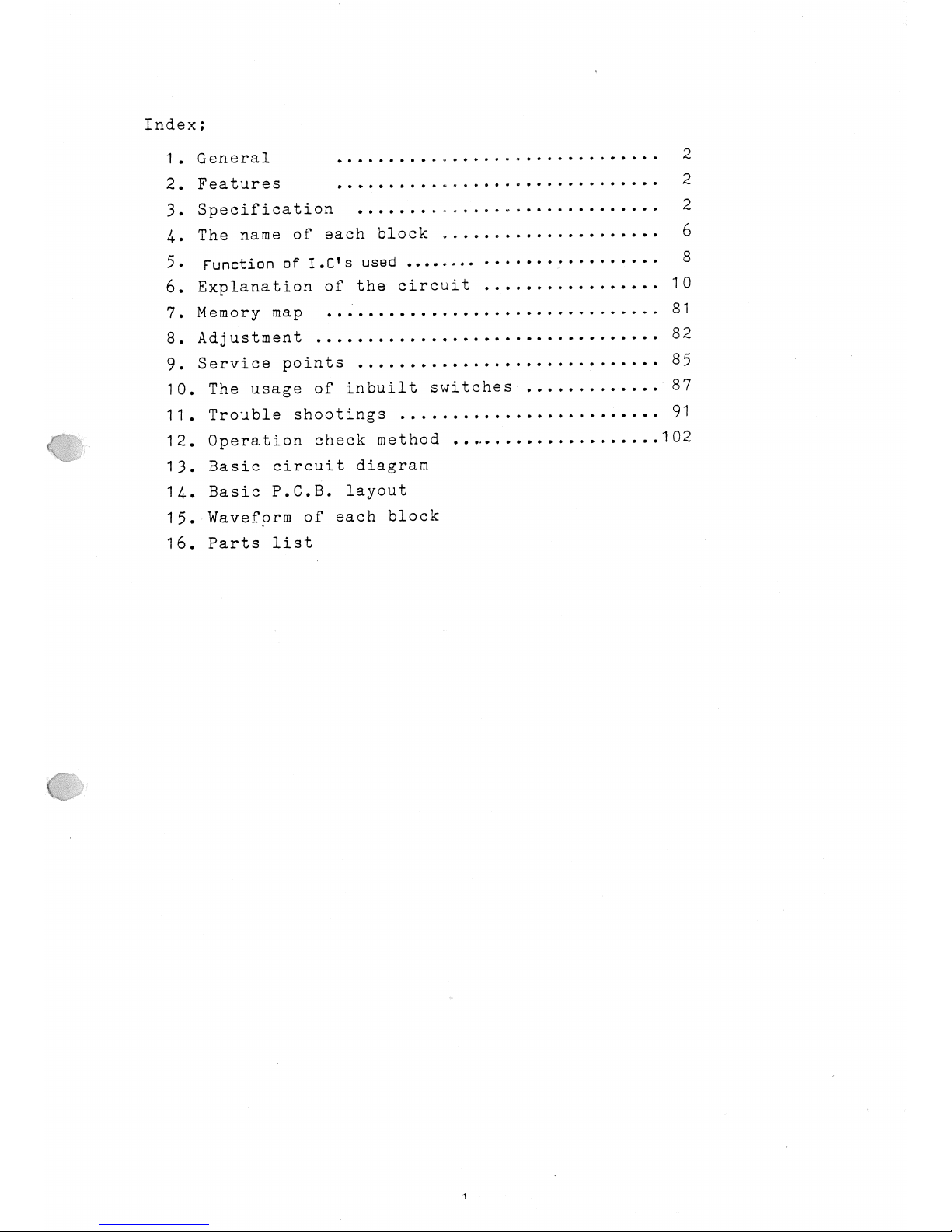
Index
1
2
3
4
5
6
7
8
9
10
11
12
13
14
15
16
a
0
a
o
0
Q
U
0
Q
u
o
0
0
0
0
»
9
General
.
2
Features
.
2
Specification
........
1
,
2
The
name
of
each
block
..
.
6
Function
of
I.C’s
used
........
»
»
3
10
Explanation
of
the circuit
..
..
Memory
map
..Q
....¢iii@;i==
..
31
Adjustment
.....
...
82
Service
points
.................
..
85
The
usage
of inbuilt
switches
..
...
87
Trouble
shootings
............
...
91
Operation
check
method
...
...102
Basic circuit
diagram
Basic
P.C.B.
layout
Waveform
of
each
block
Parts list
1
Page 4
(
Y 4
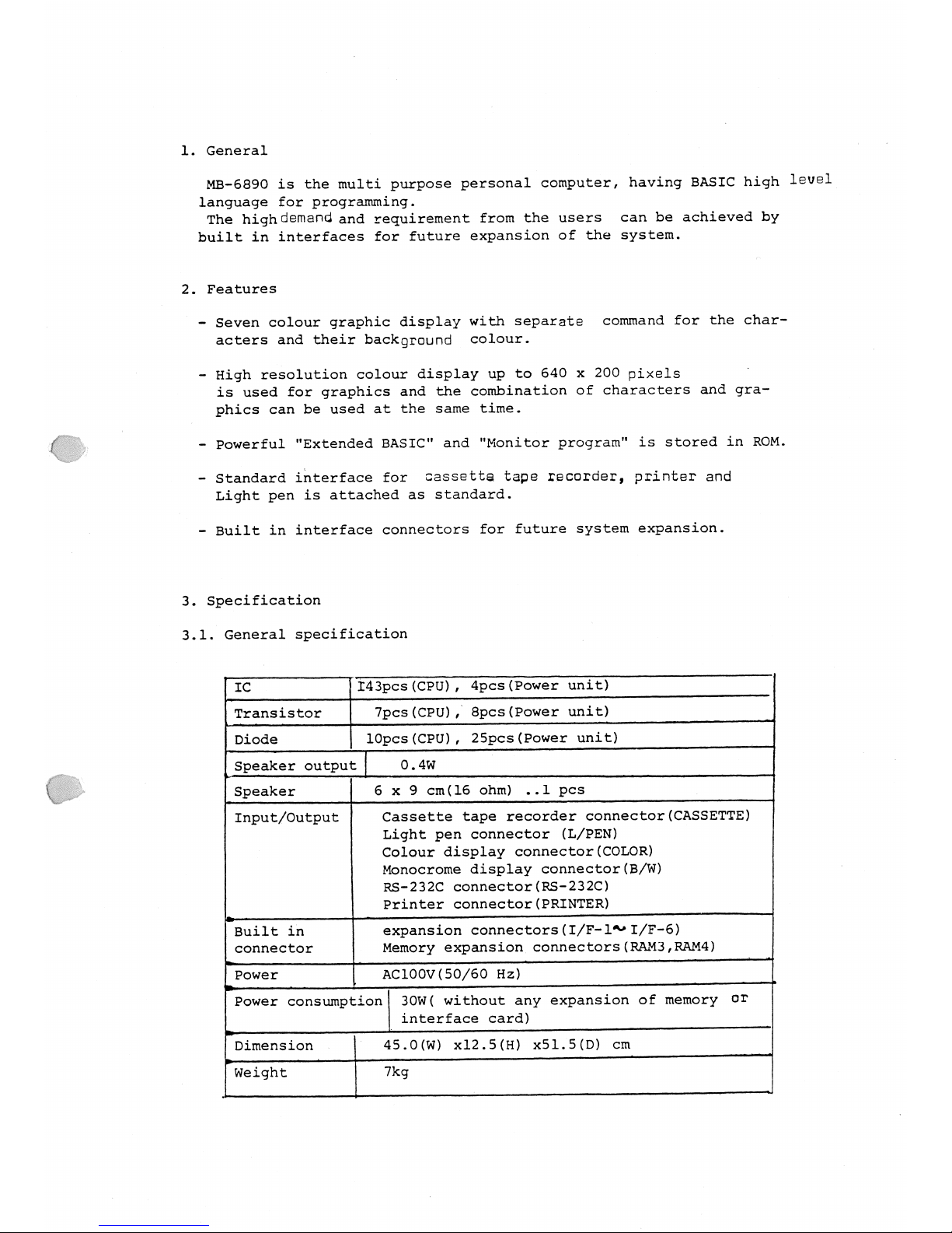
l. General
MB-6890
is the multi
purpose
personal
computer,
having
BASIC
high
language
for
programming.
The
h i g h d ‹ m ‹ H d
and
requirement
from
the users
can
be
achieved
by
built
in interfaces
for future
expansion
of the
system.
2.
Features
-
Seven
colour
graphic
display
with
separate
command
for
the
char
acters
and their
background
colour.
-
High
resolution
colour
display
up
to
640 x
200
pixels
is
used
for
graphics
and
the combination
of characters
and
gra-
phics
can
be
used
at the same
time.
-
Powerful
"Extended
BASIC"
and
"Monitor
program"
is stored
in ROM.
-
Standard
interface
for
cassette
tape
recorder, printer
and
Light
pen
is attached
as
standard.
-
Built
in
interface connectors
for
future
system
expansion.
3.
Specification
3.1.
General
specification
iIC
Wl43pcs(CPU),
4pcs(Power
unit)
Transistor
7pcs(CPU)[
8pcs(Power
unit)
p
Diode
lOpcs(CPU),
25pcs(Power
unit)
Speaker
output
O.4W
_Speaker
6 x 9
cm(l6
ohm)
_.l
pcs
I
Input/Output
Cassette
tape
recorder
connector(CASSETTE)
Light
pen
connector
(L/PEN)
Colour
display
connector(COLOR)
Monocrome
display
connector(B/W)
RS-232C
connector(RS-232C)
Printer
connector(PRINTER)
*
C
Built
in
expansion
connectors(I/F-l**I/F-6)
connector
Memory
expansion
connectors(RAM3,RAM4)
__
,
A
Power
AClOOV(5O/60
Hz)
.g
g_
.
C
,
r
Power
consumption
3OW(
without
any
expansion
of
memory
OT
interface
card)
_
_
Dimension
45.0(W)
x12.5(H)
x5l.5(D)
cm
W e i g h t
A
7kg
level
Page 5
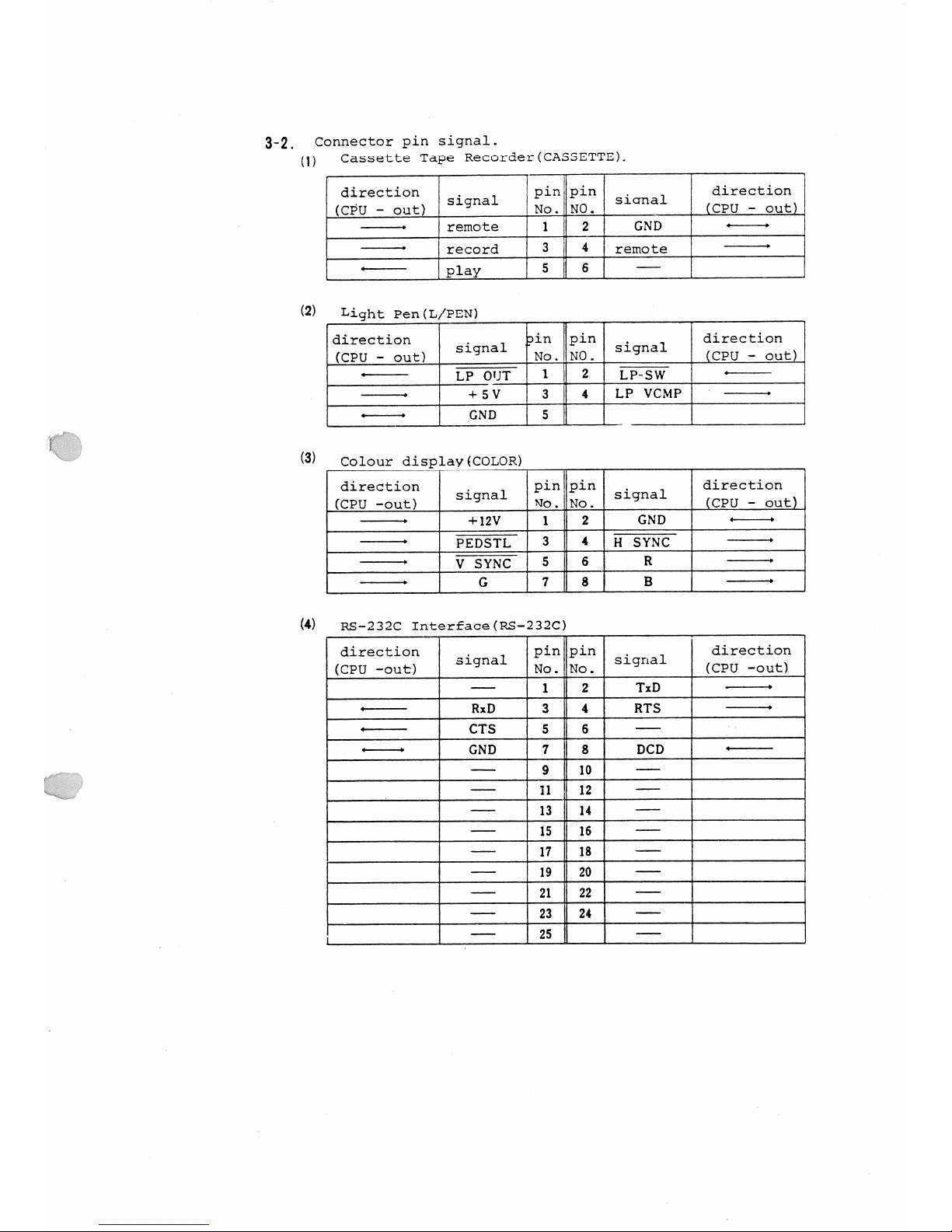
3-2_
Connector
pin
signal.
(1)
Cassette
Tape
Recorder(CASSETTEL
’W
|
direction
Signal
pin
pin
Signal
direction
(CPU
-
out)
No. NO.
(CPU
-
out
--~
remote
1
2
GUD
+--~
* - - *
record
3
4
l
remote
* - ’ *
1
* - ‘
|Play
5
6
1
_
(2)
Light
Penn./PEN)
direction
Signal
pin
pin
Signal
direction
(CPU
-
Out)
NO. NO.
(CPU
-
Out)
---
7675?
1
2
f137§vV
_ -
------
+5V
3
4
LP VCMP
‘
----
--1*
GND
5
(3)
Colour
displav(COLOR)
direction
.
pin pin
.
direction
(CPU
-out)
Slgnal
No.
No.
Signal
(CPU
-
out)
---»
+I2V
1
2
GND
#-~~»
--
T>‘§‘13§TT
3
4
QW
--
--
T565
5
’
6 R
---»
--
G
1 s B
--»
(4)
Rs-232C
Int
rfacems-232c)
direction _
pin pin
.
direction
(CPU
-out)
Signal
No. No.
Signal
(CPU
-out),
‘
*-
1
2
TxD
---*
*---
RxD 3 4 RTS
--~*
---
CTS s
e
-
i
r--
GND
7 8 DCD
- -
-
9 10
--
;
n 4 | 1
-
11
g
12
-
-~
13 14
--
’-
15 16
--
--
17
18
--
--
19 20
--
--
21 22
--
--
23 24
--
}
--
25
-
Page 6
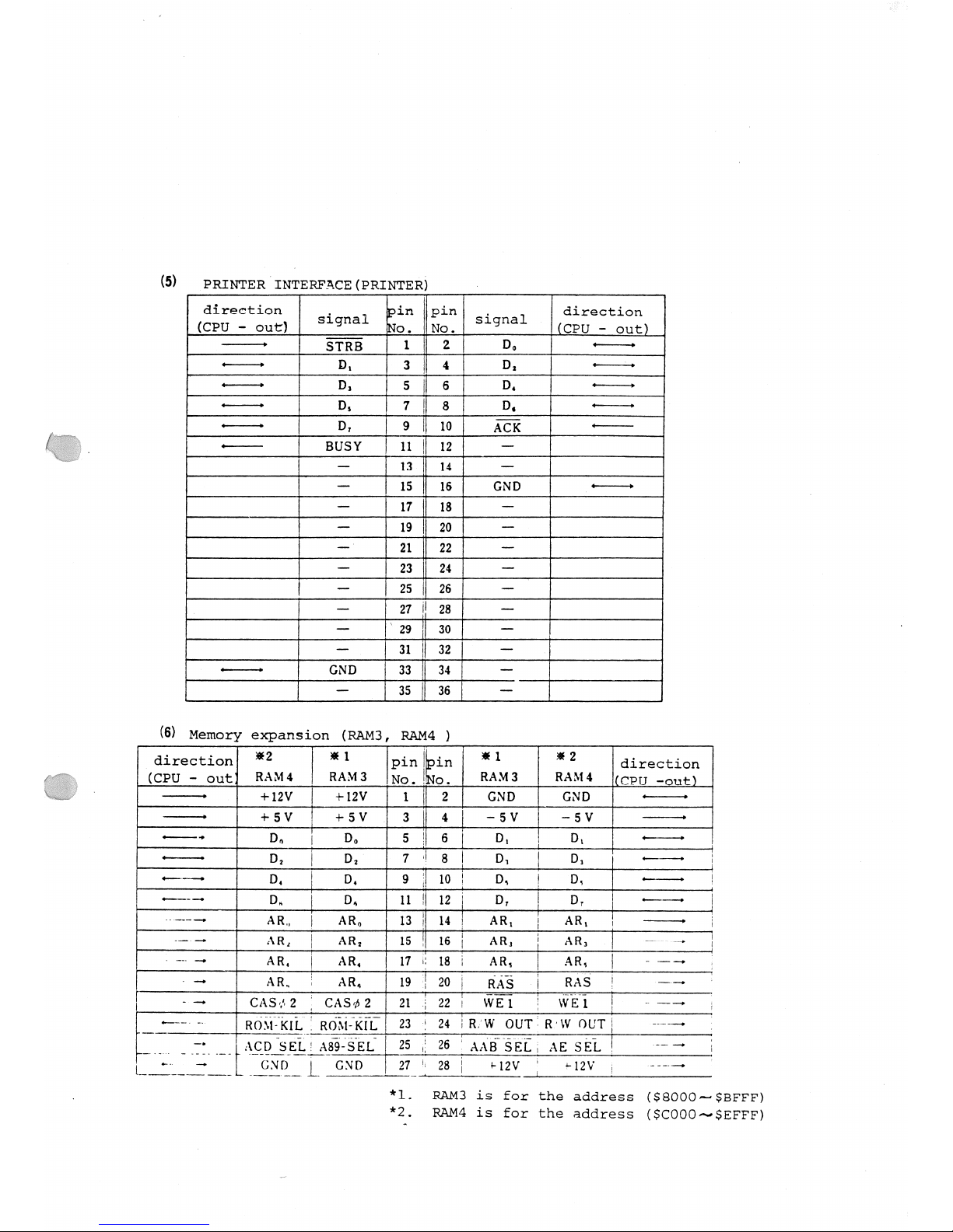
(5)
PRINTER
INTERFACE(PRINTER)
directien
.
min
Qpin
_
1
direction
V
(CPU-out)
S3151
filo.
No.
Signal
(CPU
-
out) 1
--~
STRB
1 2
D,,
-_-
--»
D,
3
_
4
D,
~_-~
---»
D,
Q
5
’_
5
D.
-_»
--~
D,
_
7
Q
s
D.
--»
--
D,
_
9
’
10
A i ; T <
--
---
BUSY
_
11
Q
12
-
Q
Q
-
,
13
Q
L4
,
-
I
I
-
_
15 15
GND
--»
-
17
0
18
-
Q
-
19 20
1
-
-
21 22
1
-
-
23 24
-
-
25
26
-
-
27
QI
28
-
-
\29
Q)
30
-
-
31Q32
-
»-_-
GND 33Q34
_
-
-
0
asQas
-
(5)
Memory expansion (RAM3,
RAM4
)
direction
*Z
*1
p i 1 1 Q
in
*I *Z
directicn
(CPU
_
QU_tI_
RAM4 RAM3
NO_
Q
O_
_
RAM3 RA114
_(CPU wut,
----»
+12v
Q
+12v 1
QQ
2
GND
Q
GND
»---
-_»
+sv
Q
+sv 3
‘
4‘
-sv
Q
-sv
---
--»
D0
Q
D0
5
Q
e
’
D,
DQ
Q
--
---
D,
Q
D,
7
3
Q
D1
D,
Q
---
--~
D.
Q
D.
9
10
Q
D, D,
--
---~»
D.
D.
11QQ12
Q
D,
D,
Q
---
»-----
A R
Q
ARD
13Q14
Q
AR, AR,
--
---»
AR,
Q
AR,
Q
15
16
Q
AR, AR,
--
--~
-
AR.
Q
AR.
_
I7
LE
18 1
AR,
AR,
_
»
--
V
-»
AR,
3
AR,
19’Q20
Q
mis
RAS
~-»
-
-»
CASQHZ
§
CAS’/52
21
22
Q
1?/E1 WEE
Q
2-
--»
*_-~~
-»
ROSFKIL
f R 0 1 1 - ‘ 1 ‹ i ’ E
23z24
QRuw
0UT§
ww
DUTQ
-s--~»
_
--
___
1 1 g D s E 1 ; e
A 8 5 - A S E I _ . _
25
.f
26
FA,11§"sE1I;
AE SEL
Q
’---
_i;N11;*Q_‘GND
0
2 7 Q _ _
28
Q
»12v
Q
»12v
~--~-»
*l,
£143 is
for
the
address
(58000
*2.
RAM4 is
for the
address
(SCOOO
SEFFF)
Page 7
75
Ihterface
expansion
(I/F-I I/F-6)
i
direction
i
_
ipinppin
,
direction
(CPU
-out)
t
Signal
No.
Signal
(cPU-
out)
-4-_~
+5v
1
1
2 GND
---
-~-»
i
D..
3
4
D,
---»
--
D,
5
i
5
D,
--»
---»
D.
1
1
s
D5
---
--»
D1
9
’
10
D,
»--»
--~
A,,
11‘12
A,
----
1
---A
A
{
A,
Q
13
Q
14
A,
|
---
~
{
---»
A.
15 16
A.
--»
---
A.,
17
18
A,
--»
4--»
A.
19 20
A.
---
----
A .
21
A
22
A,,
---
---
A.,
23 24
A,,
--»
--»
A,.
25
26
A,,
--»
-_-
BA 27
’
28
BS
-~
---
‘
E555
‘
29"so
EXROM-KIL
--~
---
11/w IN 31‘32
E356
--~
---»
R/w OUT
33A34
VMA
our
--»
--»
1-:
as
as
Q
---»
1
---
‘1§‘§
37 38
FH
----
---
T55
as 40
mi
---
EXE4142WTTEE.---
EXE
41
42
WTTEE.
---
--
ETA’
43 44
§XN‘1FSW
---
--»
HALT ACK 45 46
SOUND
IN
---
---»
‘
ISMCK
47 48
GND
f--»
---
2Mc1< 49
so
GND
1--»
--~
-5V
51- 52
‘}§;‘§‘{ffR)"§"
--->
-1-
-12v
53 54
+12V
---»
----
GND 55 56
+5v
--
5
Page 8
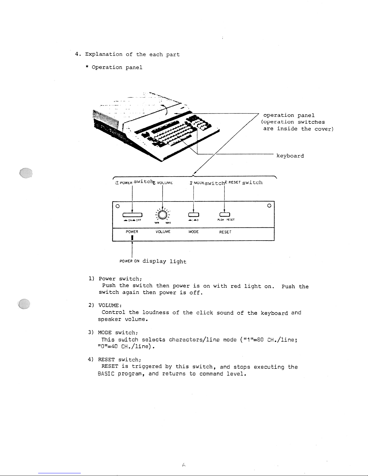
4.
Explanation
of the
each
part
*
Operation
panel
._
~»,‘
_.
.
,..,
:_
_ _
._
~"’"T
M
_
‘ _ -
»-=
’
V"
f_ _’
"
I
*
operation panel
~ W " C 5 G 5 ? ? 7 i W i ~
E
I
/
<@@fafi'H
switches
"fHfi@
~
__
_
~
are inside
the
cover)
.,’i’;i;@;_:_
N
_
-
_
’i
_
V
keyboard
*
\
(Q
eowsfz
S W 5 - C C h i
votufvia
j!MopE5wj_tC1q=?
RESET
Switch
0
}
O
_O,,,¢¢-
if \:
..;¢¢
msn
asssr
WN
MIX
POWER VOLUME MODE
RESET
Powaaon
display
light
l)
Power
switch;
Push the
switch
then
power
is
on with
red
light
on.
Push the
switch
again
then
power
is
off.
2
)
VOLUME :
Control the
loudness
of
the
Click sound
of the
keyboard
and
speaker
volume.
3)
MODE
switch;
This switch
selects
characters/line
mode
("1"=80 CH./line;
"o"=ao
CH./line).
4)
RESET
switch;
RESET
is
triggered by
this
switch,
and
stops executing
the
BASIC
program,
and returns to
command level.
A
Page 9
*
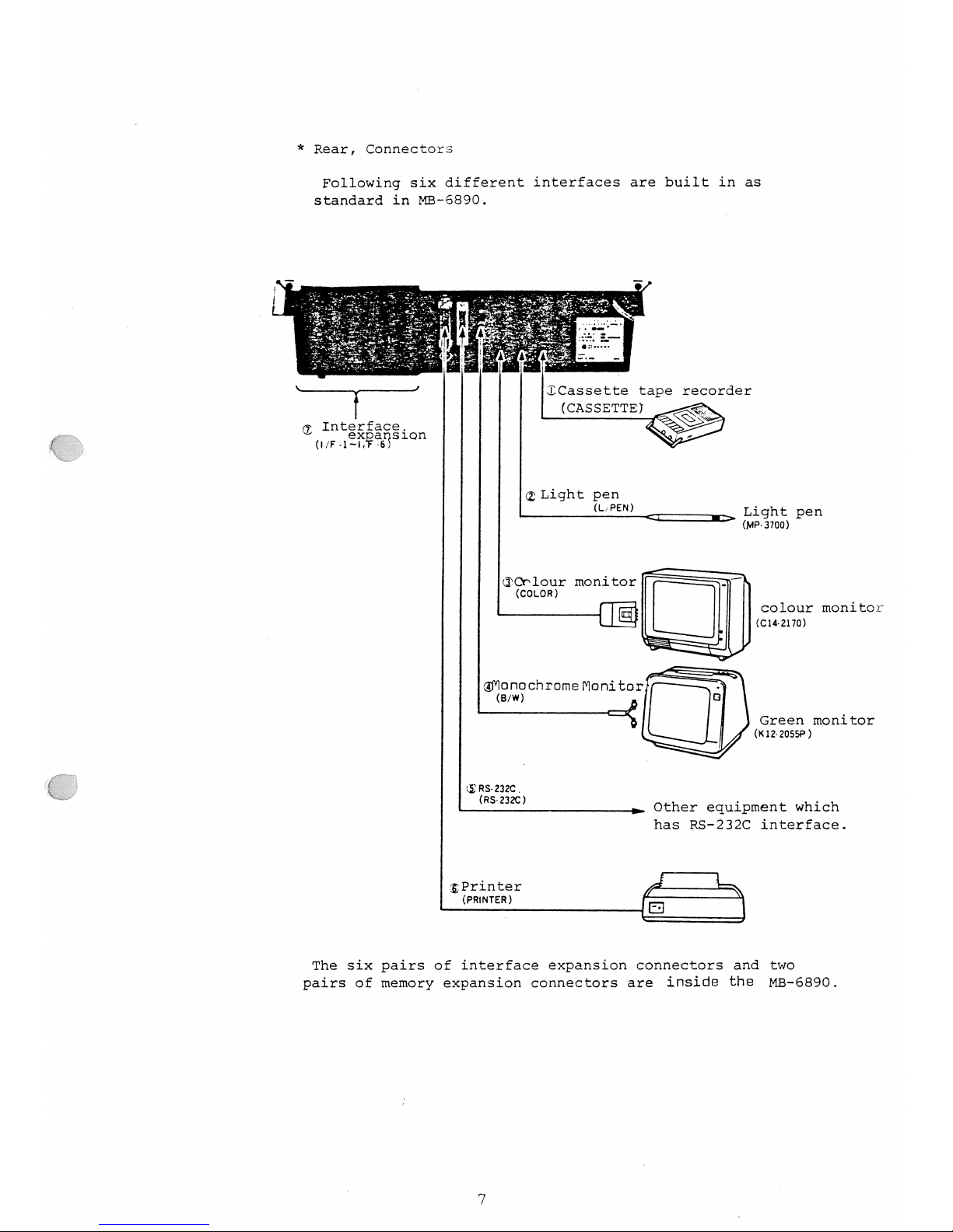
Rear,
Connectors
Following
six
different
interfaces are built in as
standard
in M -6890.
1
*
p.
mm
.H~mi»;_ __‘_
_,_
,
_
{
_
~
,
~ . ’ + = .
’ . ’ Q ~ ’ z ~ : ‹ :
’_
; ~ » ~ - =
_
f-
:""’
~
’;»
n " ¢ ’ 1 ~
‘
’»-
> ’ ~ 1 ; . " 1 ’ - : F i - k c ’ - ’ A
E§»:.-»;_
_V
T _ » " j ! , , 2 5 f " ‘
;-¢_
,_
. ,
‘?’
g’
gf
=
_ : i 2 , [ § » ; : i ; ’ § ’ + - ; § M ; i ? , ; @ 5 ’ , 2 f + l ; , 5 = i ! " 3 3 Z ’ § i : f 1 a a : H t l r f . " -
M;
i ? , ; @ 5 ’ , 2
f
+
l
; , 5 = i ! " 3 3 Z ’ § i : f 1 a a
:Htl
rf."-
, f
-if
» ¢ ~ f = t . = , \ 1 g f f , . ; - ~ - - , » f ’ ~ q ’ -
.V
’
~
~_ "F
~
’
$Cassette
tape
recorder
(CASSETTE)
,
@
Interface.
/W
ex a
sion
_
(I/F
-1~»,$-513
\/
Qlight
pen
(DPW)
__
Light pen
(BAP-3700)
fiCblour
monitor
"""i
-
(coLoR>
colour monitor
(c14-2170>
@MonochromeMonitor’
H
(ww)
B
Green
monitor
(KIZZDSSP)
5
ins-zazc.
Rs~z32c
. .
( )
Other
equipment
which
has RS-232C interface.
isprinter
(PMNTER)
The six
pairs
of interface
expansion
connectors and two
’
connectors are
inside
the
MB-6890.
pairs
of
memory
expansion
7
Page 10
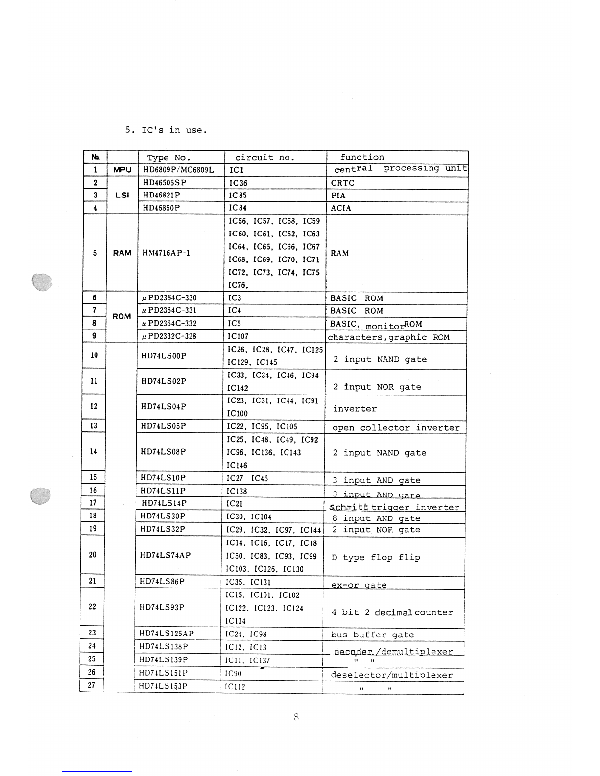
5. IC’s
in
use.
Type
No.
Q
circuit no.
function
Mpu
HDeso9P/MCeao9L
1C1 central
Pf C@SSif19
Unit
Hmssossp
rcse CRTC
L.Sl HD4ea21P
Q
LCSS
Q
PIA
Q
HD4sssoP
ICS4
ACIA
Icse,
1Cs1 Icss 1Cs9
1Cso,1Cs1
xcsz
[css
RAM HM4716AP-1
IC54’
IC65’
IC66
IC57
RAM
ICss,1Cs9
Icvo
IC71
IC12, IC73, IC14,
IC75
1C1s,
/mnzsasc-ssc
Qrcs
BASIC Rom
Q
ROM
uPD2364C-331
IC4
BASIC Rom
Q
uPD2364C-332
I C S
BASIC,
monitoraom
yPD2332C-328
IClO7
\characters,graphic
ROM
HDHLSODP
1C2s, rczs, IC47,
IC12s
2
_
IC129,
IC145
lnput
NAND
gate
Icaa,
IC34,
1C4e,
ICQ4
" D 7 L S " 2 P
[C142
2
input
NOR
gate
HDNLSMP
IC23,
IC31,
IC44,
1C91
inverter
IC100
HD74LS05P
IC22,
lC95,
ICIOS
open
collector inverter
xczs,
Icas,
xC49,
IC92
HD74LS08P
IC96, IC136,
IC143 2
input
NAND
gate
1C14s
HD74LS1OP
1C21
rC4s
3
input
AND
gate
HD74LS11P
Qrclss
3
input
AND
gm?
Q
H D 7 4 ~ 5 1 4 P
[Cm
Q
Stghmitt
trigger
inverter
V
HD74LS30P
rcso,
ICIO4
S
input
AND
gate
Q
HDm.S32P
1C29,
1C3z, IC97,
1Cl44]
2
input
NOP-
gate
IC14,
IC1s, ICI7,
IC1s
HD14Ls74AP
Icso,
xCs3, xC93,
IC99
D
type flop
flip
1C1o3
IC126.
ICl30
Q
HD14LSseP
Azcss,
[C131
eX_Or
qate
Q
1C1s, IC101.
rC1o2
Q
HD74LS93P
‘ICl22
1C123,
rC124
4 bit 2
decimalcounter
Q
IC\34
’
!
HD74LSI25AP
ICQ4,
me
bus buffer
gate
Q
HD14LS13sP
Q1C12.
IC13
_
d&m’dQr_Q/demltiplexer
HD14LS139P
ICU. IC137
-»
»~
Q
Hm4LS1sw
Q
xC9o
’
deselecwr/multiplexer
Q
HD74LS1_53P
Q 1C112
QQ
.» ~
1
3
Page 11
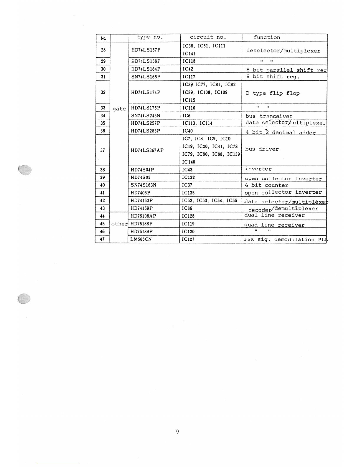
Na
type
no. circuit
no.
function
i
Icas,
IC51,
IC111
28 HD74LSl57P
ICI"
de-selector/rfzultiplexer
I
HD74LSI58P Icus
-- --
__§g_
HD14LS1e4P
IC42
8 bit
parallel
ahlft
req!
31
sN14Ls1seP
xcm
3
bit
shift
reg.
""
1ca91c11,
IC81,
xcsz
32
HD74LSl74P
rcse, ICIOS,
XC109
D
type
flip
flop
Icus
_:ET
gate
HD74LSl75P Icue
"
-’
T a sN741.s245N
arcs
bus
tranceiver
E
HD74LS257P
IC113,
IC114
data
Seleeterhultiplexe-
__§§_a
HD?"-5283? 1C4
4
bit Q
decimal
adder
1c1,
ics,
rcs,
Iclo
37 HD74LS367AP
xcle, Iczo, IC41,
lcvs
bus
driver
IC79,
Icso,
Icsa,
IC139
1c14o
Vi? HD74S04P IC43
inverter
E
H - 3 7 4 5 0 5
IIC132
J
open
collector
inverter
40
SN74S163N
IC37 4
bit
counter
’T Hrmosp IC135
open
collector
inverter
Z
Hm41s3P
1C52,
xcsa,
IC54,
IC55
data
Selecter/multiplØxe
43
HD74159P
IC86
decade):/demultiplexer
44 HD75l08AP IC128
duel
line
receiver
’Teena HD751saP IC119
quad
line
receiver
E;
HD75189P
IC120
" "
47 LMSGSCN
lC127
FSK
sig.
demodulation
PL
9
Page 12
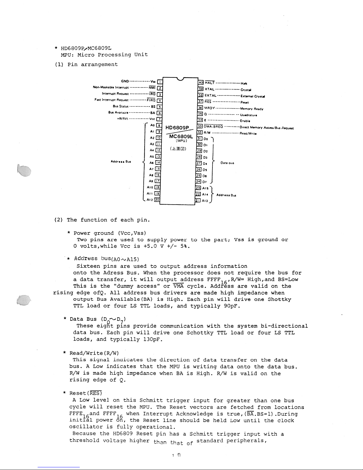
Address
DUS(AOA¢Al5)
*
HD6809P/MC6809L
MTU:
Micro
Processing
Unit
(1)
Pin
arrangement
GND------~-----V"
ll
E51HA|_r’-._--._
..-. __
H,"
Non-Mukabln
lnwrum
----- - ------
NMI
E
xYAL_
_____
___
_____ __
G y m
| \ ¢ " U 9 K
RMIUMI
~"’ - ’-"~~
I
RQ
B
gg]
SXTAL
_______
_____En
Icwnd
Pm
Immun:
Request
-~--~~~--~-
FIRQ
¢-|
gig
___ ____
_____R___t
=~=
B5
n
ss
Mm-,Y
........
-.-..M.m.,,
,.,,_,,
Bus
Avlxiauiq
-- --------
BA
B
Q
_ _ _ _ _ _ _ _ _ _ _
__
__
uu______w_
B15
---~--------
, .. ._
*
‘ V)
___
"’
’Z
"
""
" " " "
’
" "
E nabh
HD6809p
ommanso-
-~--DumMemoryAmer/au.Requen
~--Dum
Memory Amer/au.
Requen
A2
IE 3|
(MPU)
_
Do
W
A3
m
EE Dv
A4
D2
A5
D3
Addrusi
eu!
<
A.
m
D.
Dua nu,
A
’B
Ds
AU
E
E Ds
‘
A9"
E!o1)
AW
@
@ AIS
A"
m
m
A14
AddrnuEus
\A’1EE
n|Au
(2)
The
function of each
pin.
Two
pins
’
*
*
Power
ground
(Vcc,Vss)
are
used to
supply power
to the
part;
Vss is
ground
or
O
volts,while
Vcc is +5.0
V
+/-
5%.
d
to out ut
address
information
Sixteen
pins
are use
p
onto the Adress
Bus.
When the
processor
does not
require
the bus
for
t
t ddress
FFFF
R/W-
High,and
BS=Lowa data
transfer,
it
will ou
pu__a
16,
-
This is the
"dummy
access"
or
VMA
cycle.
Address are valid on the
rising edge
ofQ.
All address
bus drivers are
made
high
impedance
when
c * *
" = i l a b l e ( B A )
is
High.
Each
pin
will
drive
one
Shottky
\.J\.L\-bJ\4l¢
LJIJJ FXVQL
TTL load
or four LS TTL
loads,
and
typically 9OpF.
’d
nication
with
the
system
bi-directional
*
Data
Bus
(D-o/D7)
These
eiggt pins provi
e
commu
data
bus. Each
pin
will drive one
Schottky
TTL load or
four
LS TTL
loads,
and
typically l3OpF.
*
Read/Write(R/W)
This
signal
indicates
e
bus. A
Low indicates
that the MPU is
writing
data onto the data
bus.
R/W
is made
high impedance
when BA is
High.
R/W
is
valid on the
th
direction of data transfer on the data
rising edge
of
Q.
*
R ‹ S ‹ t ( R E S ;
A Low
level
on this
Schmitt
trigger
input
for
greater
than one bus
cycle
will
reset the
MPU. The Reset
vectors are fetched
from locations
‘
’_
-
Din
TFSEl6and
FFFFl6
when
Interrupt Acknowledge
is
true,(BA.BS-l).
ur
g
initial
power
on,
the
Reset
line should be
held Low
until the clock
oscillator is
fully
operational.
Because the HD6809
Reset
pin
has
a Schmitt
trigger input
with a
threshold
voltage
higher
than
that
of
standard
peripherals,
1 YD
Page 13
\
’k
a
simple
R/C
network
may
be
used
to reset
the entire
system.This
higher
threshold
voltage
ensures
that all
peripherals
are
out
of
the
reset
state before
the Processor.
*HALT
A Low level on
this
input pin
will cause
the MPU to
stop running
at
the
end of
the
present
instruction
and
remainhelted
indefinitely
without
loss
of data.
When
halted,
the
BA
output
is driven
High
indicat-
ing
the buses are
high impedance.
BS is also
High
which indicates
the
processor
is in the Halt
or
Bus Grant state.
*HALT
A
Low level on this
input
will cause the MPU
to
stop running
at the
end of the
present
instruction
and
remain
halted
indefinitelywithout
loss
of
data.
When
halted,
the BA
output
is driven
High indicating
the
buses
are
high
impedance.
BS
is
also
High
which indicates
the
processor
is in the
Halt
or
Bus Grant State,
Bus
Available,
Bus
Status(BA,BS)
The BA
output
is an
indication
of
an internal control
signal
which
makes
the MOS buses of the
MPU
high
impedance.
This
signal
does not
imply
that the bus will be
available for
more
than
one
cycle.
when BA
goes
Low,
an additional
dead
cycle
will
elapse
before
the MPU
acquires
the
bus.
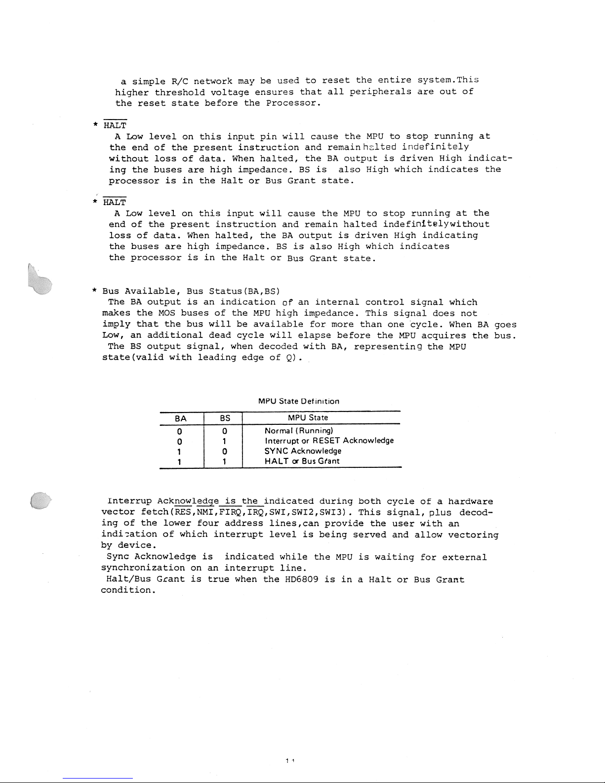
The BS
output signal,
when decoded with
BA,
representing
the MPU
state(valid
with
leading edge
of
Q).
MPU State
Definition
BA
|
as
MPU
stare
0
0
Normal
(Running)
0
1
Interrupt
or RESET
Acknowledge
1
0
SYNC
Acknowledge
1
1
HALT
or Bus Grant
interrup
Acknowledge
is
th§_indicated
during
both
cycle
of a hardware
vector
fetch(RES,NMI,FIRQ,IRQ,SWI,SWI2,SWI3).
This
signal, plus
decod-
ing
of the
lower four address
lines,can
provide
the
user with an
indication
of which
interru
t
level
‘
b
by
device.
Sync
Acknowledge
is
indicated whi
synchronization
on an
interrupt
line.
Halt/Bus
Grant is
true
when the
HD6809 is in
a Halt or Bus
Grant
condition.
p
is
eing
served and
allow
vectoring
le
the MPU is
waiting
for
external
11
Page 14

*
Non Maskable
Interrupt
(NMI)
A
negative edge
on this
input
requests
that a nonmaskable
interrupt
sequence
be
generated.
Anon-maskeble
interrupt
cannot
be
inhibited
by
the
program,
and
also
has a
higher
priority
than
E I R Q , I R Q
or
software
interrupt.
*
Fast-Interrupt
Request(FIRQ)
A
Low
level on this
input pin
will initiate
provided
its
mask
bit(F)
in
the CC
is_§lear.
over
the standard
Interrupt
Request(IRQ),and
it stacks
only
the
contents of the condition
program
counter.
*
Interrupt
Request(I§Q)
A Low
level
input
on this
pin
will initiate
provided
the mask
bit(I)
in
the
CC
is
clear.
a
fast
interrupt sequence
This
sequence
has
priority
is fast in
the sense that
code
register
and the
an
interrupt Request sequence
Since
IRQ
stacks the
entire
machine state it
provides
a
slower
response
to
interrupt
than
FIRQ,IRQ
also has a
lower
priority
than
FIRQ.
*
E,
Q
E is
similar
to
theHD468OO bus
timing
signal
§Z52;Q
is
a
quadrature
clock
signal
which leads
E.Address
from the
MPU
will
be valid
with
the
leading
edge
of
Q.
Data is
latched on the
falling
edge
of
E.
*MRDY
This
input
control
signal
allows
stretching
of
E
and
Q
to extend data
access
time.
*
DMA/BREQ
_
The
DMA/BREQ
input provides
fa
method
of
suspending
execution and
acquiring
the MPU
bus for
another
use.
Typical
uses include
DMA and
dynamic
memory
refresh. When
BA
goes
Low,
the DMA
device
should be
taken
off the
bus.
~HD45821E
(PIA
3
Peripheral
Interface
Adapter)
*
PIA
INTERFACE SIGNALS FOR
MPU
(U
pin arrangement _ ,___ __ __. ._ _ _ _ ._ _ .
K
FLA
aleuirectional
uataLD»~jU7)
(GNDHM
CA’
The
bi-directional
data Qines
PM
CM
(D6’D7)allow
the
transfer
of
PM
WOT
data
between
the
MPU and the
PIA.
PM %§
The data
bus
output
drivers are
PM R50
three
state
devices
that remain
PM RS,
in the
high impedance(off)
state
,As m
exception
when the
MPU
performs
PM
0
a PIA
read
operation.
PA1
32
D1
no HD46821P
nz
*
PIA
Enable(E)
Pm
(Pm)
DJ
The
enable
pulse,E,
is the
only
N215
FED#
I
timing signal
that is
supplied
P91
05
to
the PIA.
Timing
of all
other
PB*
D6
signals
is
referenced
to the
leading
:Es
Z
and
trailing edges
of the E
pulse.
6
Q
*
PIA
Read/wri§;e
C82
CSD
This
signal
is
generated by
the
(5\/WEE:
: RM
MPU to
control the
direction
of
T2
Page 15
data transfers
on the Data Bus.
A Low state on
input
buffers and data is transferred
from
the
signal
if
the
device
has been selected.
A
High
the
PIA for
a
transfer of data to
the bus.
The
the PIA line enables the
MPU to the PIA
on
the E
on
the
R/W
line sets
up
PIA
output
buffers are
enabled when
the
proper
address
and
the and
the enable
pulse
E are
present
*
Reset(RES)
The
active Low RES line is used
to reset all
register
bits in the
PIA to a
logical
zero Low. This line
can be used as a
power
on
reset
and
as
a
master reset
during
system operation.
*PIA
Chip
se1e
These three
input
signals
are used to
select
the
PIA. CS
and
CS
rn1~|a{- kr: Uifvln an/4 PC m11c+- Ha Tr\v.1 Fnr cc1c>/
ma-- -t
nigh
and
e-2
mu-. be ao" lor -election
transfers are then
performed
under
the
control
of
the
devgce.
Dat;
of
the E and
R/W
signals.
The
chip
select lines must be stable for
the
duration
of the E
pulse.
*
PIA
Register
Select(RSO
and
RS1)
The two
register
lines are used to select
the
various
registers
inside
the PIA. These two lines are used
in
conjunction
with
internal Control
Registers
to select a
particular
register
that is to be written
or read.
The
register
and
chip
select lines should
be
stable for the duration
of
the E
pulse
while in the
read or write
cycle.
*
Interrupt Request(IRQA
and
IRQB)
The active Low
Interrupt Request lines(IRQA
and
IRQB)
act to
interrupt
the
MPU either
directly
or
through interrupt priority circuitry.
These
lines are
open
drain(no
load
device)
. This
permits
all
interrupt requ-
est lines to be tied
together
in a wire
QR_configuration
and
accept
up
to 1.6
mA
curret from outside.
gagh
IRQ
line has two
internal
inter-
rupt
flag
bits that can
cause the
IRQ
line to
go
Low.
Each
flag
bit is associated with
a
particular peripheral interrupt
line.
Also
four
interrupt
enable bits are
provided
in the PIA which
may
be
used
to inhibit a
particular interrupt
from a
peripheral
device.
Servicing
an
interrupt by
the MPU
may
be
accomplished
by
a software
routine
that,on
a
prioritized
basis,seqentially
reads and tests the
two control
registers
in
each PIA for
interrupt flag
bits that are set.
The
interrupt flags
are
cleared(zeroed)
as a
result of an MPU Read
Peripheral
Data
Operation
of the
corresponding
data
register.
When
these
lines are used as
interrupt inputs
at least one E
pulse
must
occur from the
inactive
edge
to the active
edge
of these
interrupt
input
signal
to
condition the
edge
sense network.
If
the
interrupt flag
has been
enabled
and
the
edge
sense circuit has
been
properly
conditioned,the
interrupt
flag
will be
set
on
the next active
transition
of the
interrupt input pin.
*
PIA
PERIPHERAL
INTERFACE LINES
The PIA
provides
two 8 bit
bi-directional data
bused and four
interrupt/control
lines
for
interfacing
to
peripheral
devices.
*
Section A
Peripheral
Data(PA’~PA7)
Each of the
peripheraldata
lines can be
programmed
to act as an
input
or
output.
This
is
accomplished
by setting
a l in
the
correspond-
ing
Data
Direction
Register
bit
for those lines which
are to be
outputs.
A O
in a
bit of the
Data
Direction
Register
causes the
corresponding
peripheraldata
line
Operation,
the data
appears
directly
on
The
d a t a i n
Output
to act as
aninput.
During
an MPU Read
Peripheral
Data
on
the
peripheral
lines
programmed
to
act
as
input
the
corresponding
MPU Data Bus lines.
Register A
will
appear
on the data lines that
are
programmed
to
be
outputs.
A
logical
l written into
the
register
will cause a
High
on
the
corresponding
data line while a O
results in
T3
Page 16
*
a Low.
Data in
Output
Register
A
may
be read
by
an M?U "Read
Peripheral
Data A"
operation
when the
corresponding
lines are
programmed
as
outputs.
This data will
be
read
properly
if
the
voltage
on
the
peripheral
data
lines is
greater
than
2.0 volts
for a
logic
l
output
and less
than
0.8 volt
for a
logic
0
output.
Loading
the
output
lines
such that the
voltage
on
these
lines
does
not reach
full
voltage
causes
the data
transferred
into the MPU on
a
Read
operation
to
differ from
that contained
in the
respective
bit of
Output Register
A.
Section
B
Peripheral
Data
(PBSPB7)
The
peripheral
data
lines on
the B Section
of the PIA can
be
programmed
to
act
as either
inputs
or
outputs
on a similar
manner to
P A P A 7 .
However,
the
output
buffers
driving
these lines differ from
Qhose
driving
lines
P A 5 P A 7 .
They
have
three state
capability,allowing
them to enter
a
high
impedance
state
when the
peripheral
data
line is used as
a
input.
In
addition,
data
on the
peripheral
data lines
PB6»PB7
will be
read
properly
from
those
lines
programmed
as
outputs.
As
outputs,
these
lines are
compatible
with
standard
TTL and
may
also
be
used as
a
source
of
up
to 2.5
milliampere(typ.)
at 1.5
volts to
directly
drive
the
base of a
transistor switch.
*
Interrupt
Input(CA1andCB1)
Peripheral Input
lines
CAl
and
CA2
are
input
only
lines that set the
interrupt flag
of
the control
registers,
The active transition
for these
signals
is also
programmed
by
the two control
registers.
*
Peripheral
Control
(te2)
TheD91‘iDh91‘controllineCAcanbeprogrammedtoactasan
control
line CA can
be
programmed
to act as
an
interrupt input
or
asa
D9fiDh9%5l
control
output.
As an
output,
this
line is
compatible
with standard TTL. The
function of this
signal
line
is
programmed
with Control
Register
A.
*
Peripheral
Control(CB2)
Peripheral
COntrol
line
CB2
may
also
be
programmed
to act as
an
inter-
rupt input
or
peripheral
control
output.
As an
input,this
line has
High
input impedance
and is
compatible
with standard TTL.
As an
output
it
is
compatible
with standard
TTL and
may
also be used of
up
to 2.5
mill-
iampere(typ.)
at 1.5 volts
to
directly
drive
the base of a transistor
switch. This
line is controlled
by
Control
Register
B.
(ACIA
3
Asynchronous
Communication
Interface
Adapter)
W)
Pin
arrangement
(GND)
Vss
Rx
Dafa
RICLK
TxCLK
EE
Tx
Dau
EE
Gm
as
(31
M
(5V)V¢c
2
7
HD4685OP
MCM)
2;
23
E5
E5
Do
D1
D7
DJ
D4
Ds
D7
/W
||
||
ll
|$
EE
El
E5
||
I5
El
Ds
IE
@
~
E
R
SIGNAL FUNCTION
*
Interface
Signal
for MPU
*
Bi-
Directional Data
Bus(DO\D7)
The
bi-directional data
bus(DOf
D7)
allow
for data
transfer
between
the ACTA and the MPU.
The data bus
output
drivers are
three state
devices
that in the
high
impedance(off)
state
;xC9Dt
when
the MPU
perform
an ACIA
YDZA nnnrnØ-inn
..~..\..tA
vrf\.._\.r~.a.v|».
Page 17
*
Enable(E)
The
Enable
signal,E,
is a
high impedance
TTL
compatible
input
that
the bus
input/output
data
buffers and
clocks data
to and
from
the
ACIA.
*
Read/Write(R/W)
The
R/W
line is
a
high
impedance
input
that is
TTL
compatible
and
is
used to
control the
direction of data
flow
through
the
ACIA’s
input/output
data bus
interface,
When
R/W
is
High(MPU
Read
cycle),
ACIA
output
drivers
are
turned on and
a
selected
register
is
read.
when it
is
Low,the
ACIA
output
drivers are turned
off
and
the MTU
writes into a
selected
register.
Therefore,
the
R/W
signal
is
used
to select
read
only
or write
only
registers
within the
ACIA.
*
chip
Select(CSO,CSl552)
These three
high impedance
TTL
compatible
input
lines
are
used
to
address
the
ACIA. The
ACIA is
selected when
CSO
andCS1
are
High
and
CS2
is
Low.
*
Register
Select(RS)
The RS line is
a
high impedance input
that is
TTL
compatible.
A
High
level is used to
select the
Transmit/Receive
Data
Registers
and a Low level the
ControVStatusRegisters.
The
R/W
signal
line
is used in
conjunction
with
Register
Select
to
select the
read
only
register
in
each
register pair.
*
Interrupt
Request(TR5)
IRQ
is a TTL
compatible,open
drain(no
internal_pullup),active
Low
output
that is
used to
interrupt
the
MPU. The
IRQ
output
remains
Low as
long
as
the cause
of the
interrupt
is
present
and the
app-
ropriate
enable within
the
ACIA is
set.
*
Clock
INputs
Separate
high impedance
TTL
compatible
inputs
are
provided
for
clocking
of
transmitted and
received
data.
Clock
frequencies
of
l,
16 or 64
times the
data
rate
may
be
selected.
*
Transmit
Clock(Tx CLK)
The
Tx CLK
input
is used
for the
clocking
of
transmitted
data.
The
transmitter
initiates data
on the
negative
transition
of
the
clock.
*
Receive
Clock(Rx CLK)
The Rx
CLK
input
is
used for
synchronization
of
received
data.
(In
the Ø l
mode,
the clock
and data
must be
synchronized
extern-
ally.)
The
receiver
samples
of
the data on
the
positive
transition
of the
clock.
*
Serial
Input/Output
Lines
*
Receive
Data(Rx
Data)
The
Rx
Data line is
a
high impedance
TTL
compatible
input
through
which
data is
received in
a serial
format.
Synchronization
with
a
clock
for
detection of
data is
accomplished
internally
when
clock
rate
are
in the
range
of
O
to SOO
kbps
when
external
synchroniza-
tion is
utilized.
*
Transmit
Data(Tx
Data)
The
Tx
Data
output
line’transfers
serial data
to
a modem
or other
peripheral.
Data
rates in
the
range
of O
to
500
kbps
when
external
synchronization
is
utilized.
N
T5
enables
Page 18
Modem
CC>ntrol
The
ACIA
includes
severa
a
peripheral
or
modem.
The
functions
included
are
CTS,RTS
andDCD.
l functions
that
permit
limited
control
of
Clear to
Send(CTS)
This
high
impedance
TTL
compatible
input
provides
automatic
control
of the
transmitting
end of
a communications
link via
the
modem CTS
active
Low
output by
inhibiting
the
Transmit
Data
Register
Empty(TDRE)
atatus
bit.
Request
to
Send(RTS)
The
RTS
output
enables
the
MPU to control
a
peripheral
or
modem via
the data
bus.
The
RTF;
output
corresponds
to the
state
of the
Control
Register
bits
CRS and CR6.
When CR6=O
or
both CR5
and
CR6=l,
the
RTS
output
is
Low(the
actiire
state).
This
output
can
also
be used
for
Data
Terminal
R e a d y ( D 1 R )
t
Data
Carrier
Detect(DCD)
This
high
impedance
TTL
compatible
input
provides
automatic
control,
such
as
in_the
receivingirld
of
a communications
link
by
means
of
a
modem
DCD
output.
The
DCD
input
inhibits
and
initializes
the
rec-
eiver
section
of
the ACIA
when
High.
A Low to
High
transition
of
the
DCD
initiates
an
interrupt
to the MPU
to indicate
the
occurrence
of
a
loss of carrier
when the Receiver
Interrupt
Enable
bit
is set.
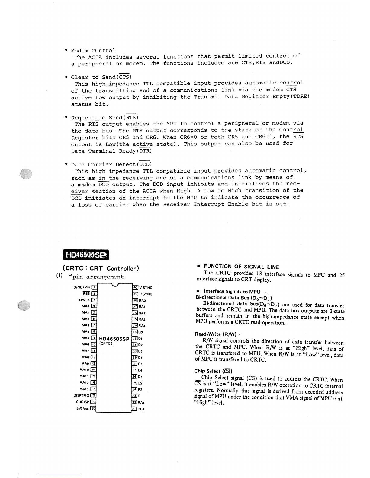
(U
p i n
arrangement
(GND)
Vss
RES
LPSTB
MAG
MAI
MA2
A4
MAS
As
MAT
MAB
A9
MA10
MAH
MAI
2
MAI]
DISPTMG
CUDISP
(5VI
Voc
_
E
E-E
HD46505SP
(CRTC)
EE
v
svnc
H
svmc
nm
nm
RA2
mu
cn
oz
I
I
l
I
Ds
I
Es‘
,
l
IEE mw
Ell CLK
(CRTC
3
CRT
Controller)
ll
4
5
B
EH
MAJ
RAA
M
El
Do
E]
EE
M
IE
gn
Ill so
D3
’2
29
D4
M
Il]
as os
IB
27
S
25
D1
E as
if
z
as
23
E
I
FUNCTION
OF
SIGNAL
LINE
The
CRTC
provides
13
int
f
’
al
interface
signals
to
CRT
d i s p l a y .
ace
sign
S
to MPU
and
25
0
Interface
Signals
to
MPU
.
Bi-directional
Data
Bus
(D0~D.,)
b
t B ! ‘ d ’ e C £ I n 3 l
data
b U 5 ( D o " D 1 )
are
used
for
data
transfer
br;/een
ide
CRTC and
Ub;1PU.
The
data
bus
outputs
are
3-state
ers an
remain
in
e
high-impedance
state
exce t
when
MPU
performs
a
CRTC
read
operation.
P
Read/Write
(R/W)
/
R/W
signal
controls the
direction
of
data
transfer
between
the
CRTC
and
MPU.
When
R/W
is
at
H i g h
level,
data
of
CRTC IS
transfered
to
MPU.
When
R/W
is
at
L o w
level
data
of MPU
is
transfered
to
CRTC.
’
Chip
Select
(C_§)
_Chip
Select
signal
(CS)
is
used
to
address
the
CRTC,
When
CSIIS
at
L o w
level,
it
enables
R/W
operation
to
CRTC
inremaj
ff¢5I5i¢f5-
N o f m a u l
this
Signal
is
derived
from
decoded
address
signal
of
MPU
under the
condition
that
VMA
sigial
ot‘MPU
is
at
H i g h
level.
Page 19

Register
Select (RS)
Register
Select
signal
(RS)
is
used
to
select
the
address’
register
and
18
control
registers
of
the
CRTC.
When
RS is
at
L o w
level,
the
address
register
is
selected
and
when
RS
is
at
H i g h
level,
control
registers
are
selected.
This
signal
is
normally
a
derivative
of
the
lowest
bit
(AO)
of
MPU
address bus.
Enable(El
Enable
signal
(E)
is
used
as
strobe
signal
in
MPU
Rfw
operation
with
the
CRTC
intemal
registers.
This
signal
is
normally
a
derivative
of the
HMCSSSOO
System
95;
clock.
Reset
(lil
___
Reset
siglal
(RES)
is
an
input
signal
used
to
reset
the
CRTC.
When
RES
is
at
L o w
level,
it
forces
the CRTC
into
the
following
status.
~
_ _ _ _ _
1)
All
the
counters
in
the
CRTC
are
cleared
and
the
device
stops
the
display
operation.
2)
All
the
outputs
go
down
to
L o w
level;
3)
Control
registers
in
the
CRTC
are
not
affected
and
remain
unchanged.
This
signal
is
different
from
other
HMCS6800
family
LSls
in the
following
functions
and
has
restrictions
for
usage.
1)
RES
signal
has
capability
of
reset
tiinction
only
when
LPSTB
is
at
L o w
level.
2)
The
CRTC
starts
the
display
operation
immediately
after
RTS
signal
goes
H i g h " .
0
lnterfage
Signals
to CRT
Display
Device
Character
Clock.
QCLK)
CLK
is
a standard
clock
input
signal
which
defines
character
timing
for
the CRTC
display
operation.
This
signal
is
normally
derived
from
the external
high-speed
dot
timing
logic.
Horizontal
Sync (HSYNC)
HSYNC
is
an active
H i g h
level
signal
which
provides
horizontal
synchronization
for
display
device.
Vertical
Sync
NSYNC)
VSYNC
is
an
active
H i g h
level
signal
which
provides
verti-
cal
synchronization
for
display
device.
Display
Timing
(DISPTMG)
DISPTMG
is
an active
H i g h
level
signal
which defines
the
display period
in
horizontal
and vertical
raster
scanning.
It is
necessary
to enable
video
signal
only
when
DISPTMG
is
at
l ’ l i g h "
level.
Refresh
Memory
Address
(MA0~MA13)
_
MA0~MA,,
are refresh
memory
address
signals
which are
used
to access
to refresh
memory
in order
to refresh
the CRT
screen
periodically.
These
outputs
enables 16k
words
max.
refresh
memory
access.
So,
for
instance,
these are
applicable
up
to
2000
characters/screen
and
8-page
system.
Raster
Address
(FlA0~RA4)
RA4,~RA.,
are
raster
address
signals
which
are used to
select
the
raster of
the character
generator
or
graphic
pattem
generator
etc.
Cursor
Display
(CUDISP)
CUDISP
is
an active
H i g h
level video
signal
which is
used
to
display
the
cursor
on the CRT screen.
’This
output
is in-
hibited
while DISPTMG
is
at l o w
level.
Normally
this
output
is mixed
with
video
signal
and
provided
to the
CRT
display
device.
Light_Pen
Strobe
(LPSTB)
LPSTB
is
an
active
H i g h
level
input
signal
which
accepts
strobe
pulse
detected
by
the
light pen
and control
circuit.
When
this
signal
is
activated,
the
refresh
memory
address
(MA,,~
MAH)
which
are shown
in
Fig.
2 are
stored
in
the
14-bit
light
pen
register.
The
stored
refresh
memory
address need
to be
corrected
in
software,
taking
the
delay
time
of
the
display
device,
light
pen,
and
light
pen
control
circuits
into account.
(16,384
BIT
DYNAMIC RAM)
’iff’ 255;
Dan
Ag
A,
A.
A,
H
*
Direct
access
of
l6l
memory by
7
E
El
E
lj
B
address
line(A6~A6)
can
not
be
done.
For
that
reason,
select
one
line
in
2
=l28
under
RAS
mode,
then
select
one
row
from
2 =l23 under
CAS
mode.
I
E] E1
E)
B
thus_select
one
from
l28xl28=l6,384
vu_o___
Dm
wg
nag
A0 A;
A
__\;o_c:
COlllblI’lB.l11Ol.’l..
U...
.....
galqrnw
*
The
corresponding
state
of
each
signal
Dom
-»-Dave OovWY
N>A6~
E"-Wf’9?11
El\UDl9’
FMS
--~~#
Fon Amress Seleul
U3--~Cc|um
Address
Selecn
pin
is as
follows;
RAS...
Low
level;
line
selection
mode
CAS...
Low
level;
row
selection
mode
’V~lE_..
Low
level;
write
mode,
the
data
from
D.
is written
in
RAM.
High
level..
read
mode,
the
data
from
l i l - I M
is read
through
D
out
Page 20
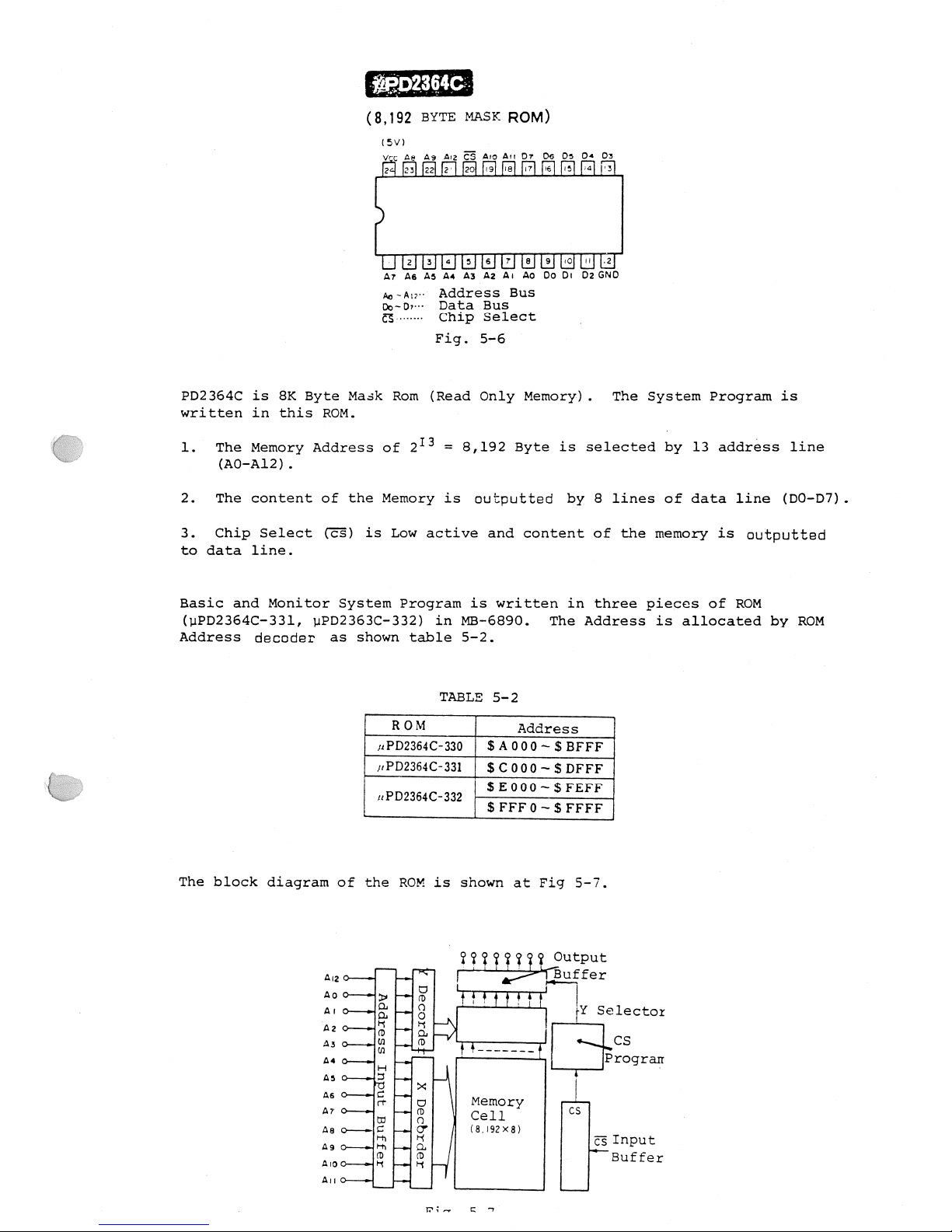
(8,\92
BYTE
MASK
Rom)
(5v)
V.-C
A9
A9 Aszgmo
Arr D1 D6 D5
D4 D3
& @BE B
BBEBB BEBN
I
Ar As A5
A4
A3 A2
An
Ao Do Du Oz
GND
A.»~Aw-»
Address
Bus
m~D~-
Data Bus _
----- ChipSelect
-----
Chip
Select
Fig.
5-6
PD2364C
is
SK
Byte
Mask Rom
(Read
Only Memory)
_ The
System Program
is
written in this
ROM.
I3
8 192 B te is selected
by
13
address
line
1. The
Memory
Address
of
2
=
,
y
(AO-Al2)
.
2. The content of the
Memory
is
outputted
by
8 lines of data line
(DO-D7)
3.
Chip
Select
(EE)
is Low
active and content of the
memory
is
outputted
to data line .
Basic and Monitor
System
Program
is
written
in
three
pieces
of ROM
(uPD2364C-331, pPD2363C-332)
in
MB-6890. The Address is
allocated
by
ROM
Address
decoder
as shown
table 5-2.
TABLE
5-2
R OM
I
Address
/1PD2se4c-aao
|
$
A
oo
o
~
s BFFF
,,PDz3e4c-331
1
s
c
ooo
~
s n1=z=1=
i »~ v- ~ - -
A
--Q-QQ
u P D 2 3 6 4 C 3 3 2
L"UU
5
bb"
s
FFF
o
~
s
FFFF
The block
diagram
of the ROM is shown
at
Fiq
5-7.
212
Output
M2
Buffer
A0
->
3
1
A»
o-Ag
_.Q
YY
Selector
A2
o-+3
-.
3.
A5
o-_~$
_.L_f1D_
_______
CS
M
Q_..H
_.r-’
PrOqra;r
A5
S33
_>
A6
fi
E;
Memory
A
AT
m 3
CS
Aao->C.’
_>O’
(8,l92>
A9
_.’S2
__
E1
5
P W C
.. O_.2
,Q
Buffer
\
A||;¢-L
i.._..¥
¥7§~
E
-1
Page 21
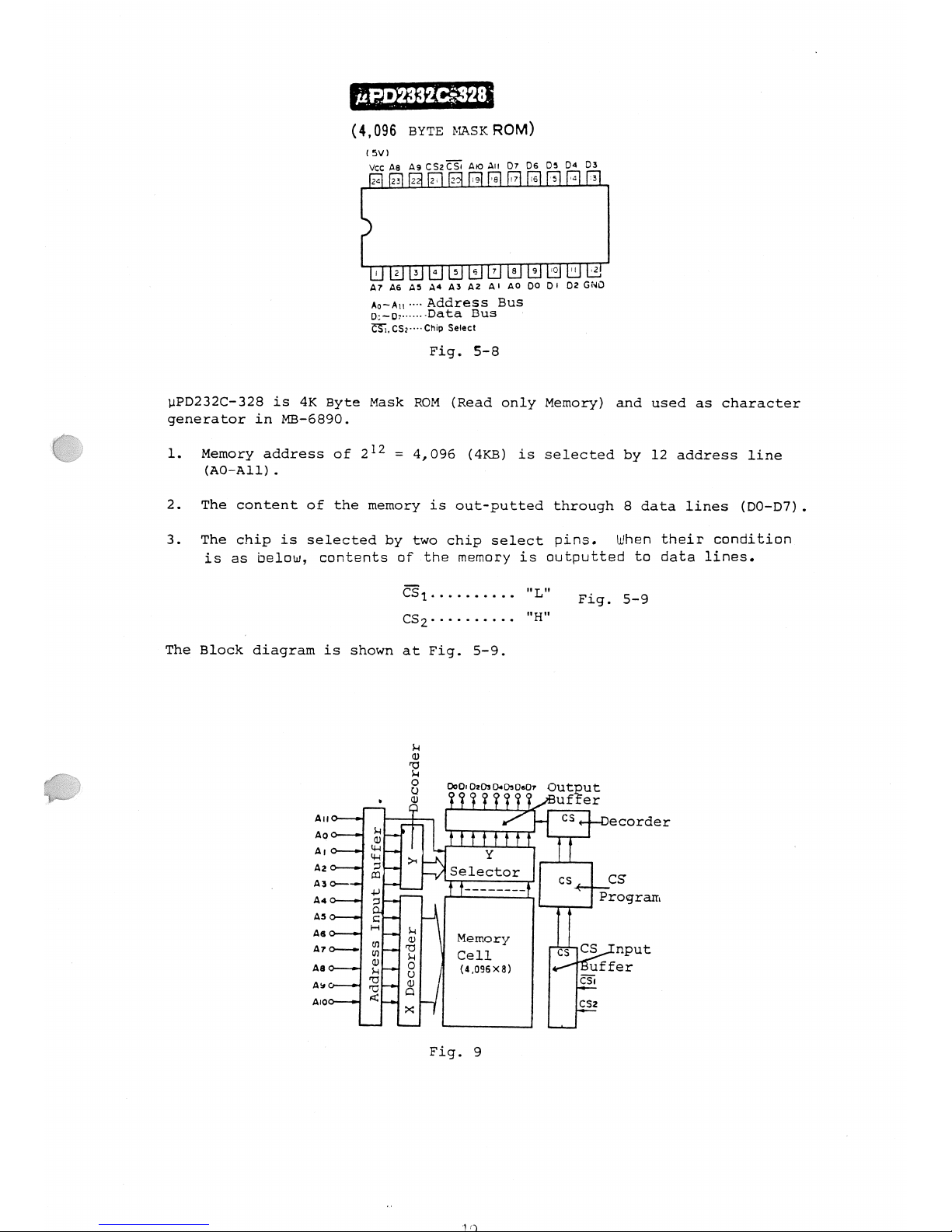
’igl?Q2332C»§328,§,
(4,096
BYTE
MASK
Rom)
:sw
v¢¢Ae
Ae
CSZEEE
Ao
Au
D1
os os
O4
os
EER E !
I B E EIEEU
A7
As
A5
A4 A5 AZ
Au
AO
D0
D’ DZGNU
M _ A
-~~-
Address
Bus
m_g,
......
.Data Bus
f5T.CSz
---~
Chip
Select
Fig.
5-8
uPD232C-328
is
4K
Byte
Mask
ROM
(Read
only
Memory)
and used
as character
generator
in M -6890.
1.
Memory
address of
212
=
4,096
(4KB)
is
selected
by
12
address
line
(A0=All}.
2.
The content of the
memory
is
out-putted
through
8
data lines
(DO-D7)
Fig.
9
1
1]
Page 22
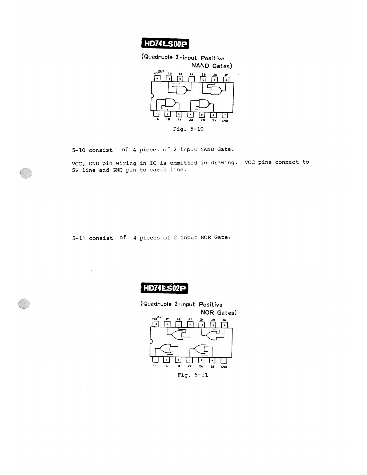
HDZQEQS
OUP
(Quadfllpfe
2‘i|’1DUt
Positive
NAND
Gates)
WØsw
B dA
Av
33
3,
3,
U
U
U
I
B
U
I
" "
’
E-1
*h
’
l’_
nnuunn
’lilvugeavgns
Fig.
5-10
5-10 consist
of 4
pieces
of
2
input
NAND
Gate.
VCC,
GND
pin
wiring
in IC
is omitted
in
drawing.
VCC
pins
connect
to
SV
line and GND
pin
to earth
line.
5-11
consist
of
4
pieces
of
2
input
NOR
Gate.
(Quadrupie
2-input
positive
)
_
NOR
Gates)
vcc(5V
av
ag 4,
3,
Ja M
.,‘, ,¢)_
QTQT
ii
u
»
v
PA
|g 21
25
Gm
Fig.
5-11
Page 23
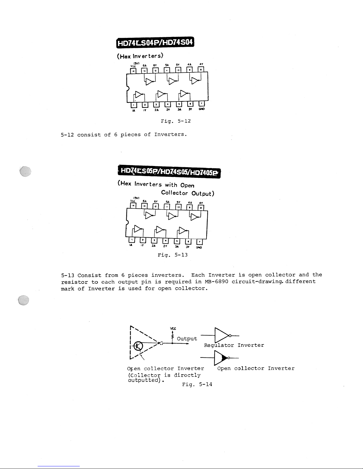
Hn74r.su4e/HD14su4
(Hex
Inv
er
ter
S)
s v
GA
sv
5A
5V
ll
V
I
ll
ll
li
ll
ll
P>
P*
I
Vcc
m
P’
P’
P’
ll
’H’
Fig.
5-12
5-12 consist
of
6
pieces
of
Inverters.
HDl4ES05E/HDZ4s05/Hnz4o5g
(Hex
Inverters
with
Open
CoHector
Output)
(sw
vc:
SA
51
54
5’
A
Y
5|
lF.’§l
II
IH
ll
ll
>
"
’F
li
li
u
II
II
I
IA
nv
Fig.
5-13
5-13 consist
from
6
pieces
inverters.
Each Inverter
is
open
collector and
the
resistor
to
each
output
pin
is
required
in MB-6890
circuit-drawing.different
mark
of Inverter
is
used for
open
collector.
"\
WDC
I
‘\\
:
\\
_
Output
|
/»"
Regulator
Inverter
|
//
v"\
Open
collector
Inverter
Open
collector
Inverter
(Collector
is
directly
outputted).
Fig.
5-14
Page 24
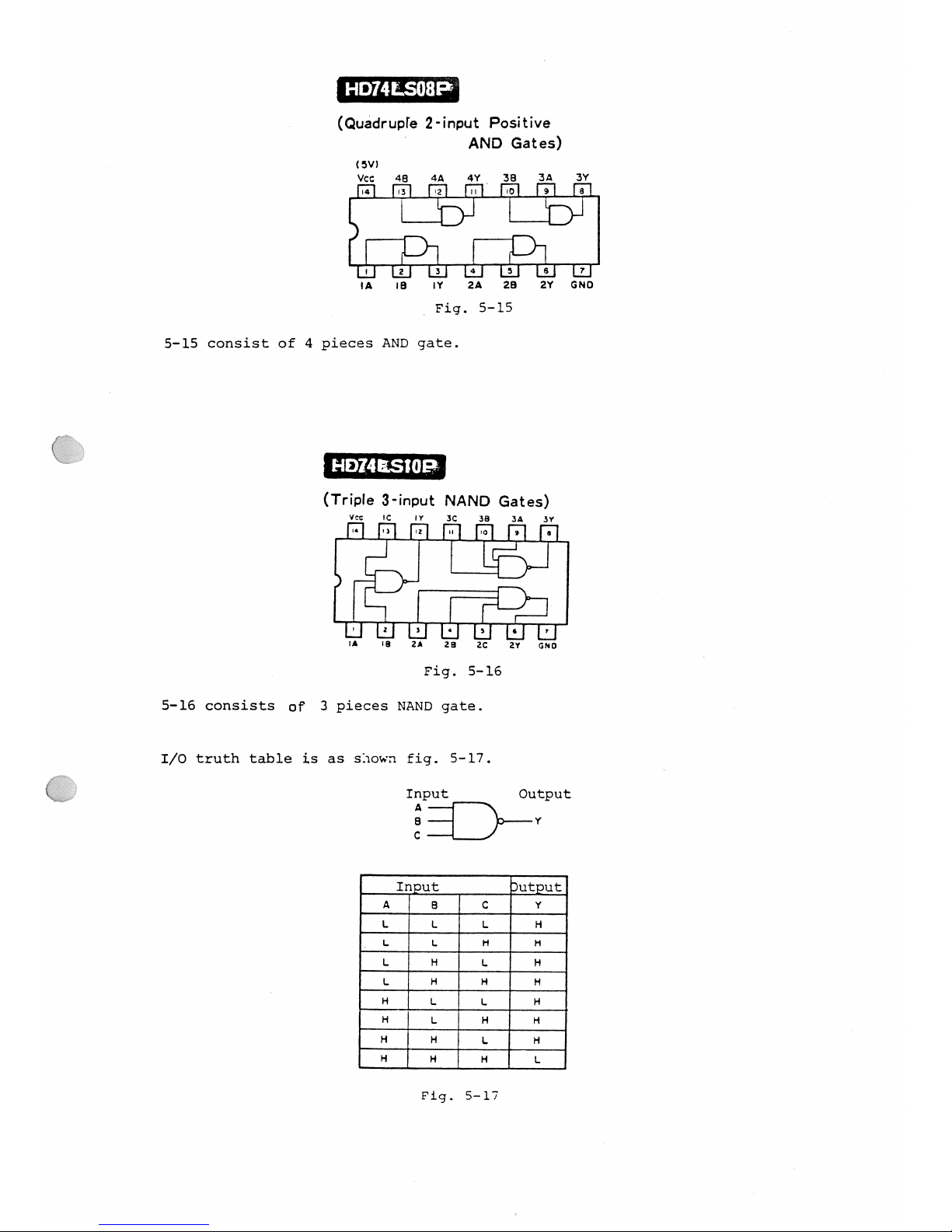
HD74l;S08F¥‘
(Quedrupfe
2-input
Positive
A
AND
Gates)
(svn
vc:
45
4A
avg
BB
BA sv
ml ’»3|
12
II
IO
9 a
§¢;
4
5
s
U:
IA IB
IY 2A
28 ZY GND
Fig.
5-15
5-15
consist of
4
pieces
AND
gate.
(Triple
3-input
NAND
Gates)
ve:
IC IY
_Sc
38
IA
5v
14|
I)
12 1|
ro
9
3
W’
I
l
1
S
V
C
I
7
ll
IB ZA
ZS
2C
ZY
GND
Fig.
S-16
5-16
consists
gf
3
pieces
NAND
gate.
I/O
truth table
is
as
shown
fig.
S-17.
Input
Output
Q
Y
c
In
ut
utput
V A p B l C
Y
L}L
L H
.LIL
H H
L|H|L
H
L H
\
H
H
HLIL
H
:HTL
H
H
HlH|L
H
HIHIH
L
Fin; 5-11
U
Page 25
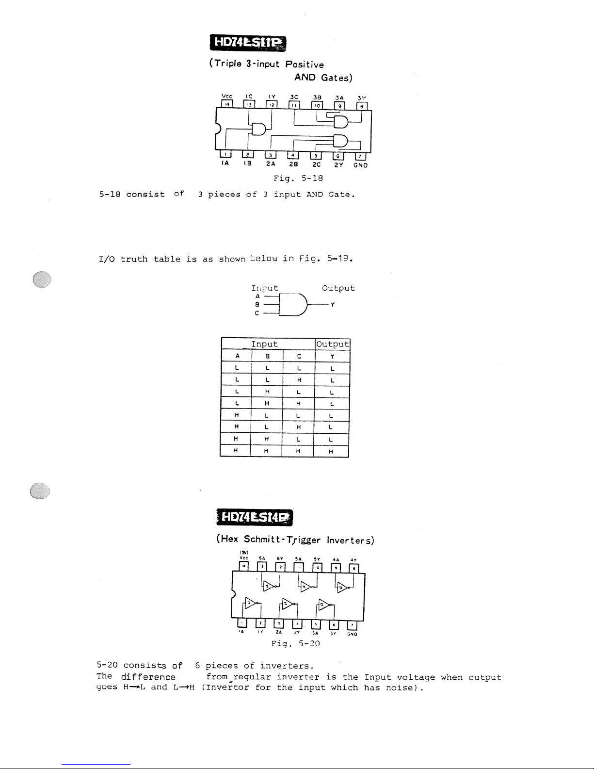
H’5?14¢$;l¥F§,.
(Triple
3
-input
Positive
g
H
L
L
L
AND
Gates)
Vcc IC IY
3C
38
V;/A
3Y
gal
II?
Ed
I
’
Lil
»
’I
2
~1
5
Is[’Ir
IA
IB
ZA
za
2C
2Y
GND
Fig.
5-18
5-18
consist
QF
3
pieces
of 3
input
AND
Gate.
I/O
truth table is
as shown
below
in
Fiq-
5-19-
Input Output
A
____
B Y
C
_
lnput
Output
I
A
I
a
c Y
L
I
L
I
L
L
L
L H
L
I
L H
L
L
L
I
H
H
L
H
H
l.
L
H
H
H
H
I
I
H
L
I
H L
I
I
(Hex
Schnutt-TjiggerInverters)
ISI)
Vcc
SA
SY
SA
5v
4,5
,gy
,I
,
Ii
I
I
I
I
I
I
I
I
’l
If
ZA
ZY
BA
Sv
Quo
Fig.
5-20
5-20
consists
of
5
pieces
of inverters.
The
diffgpengg
from
regular
inverter
is
the
Input
voltage
when
output
goes
H-#L
and
L-#H
(Inverter
for the
input
which has
noise).
Page 26
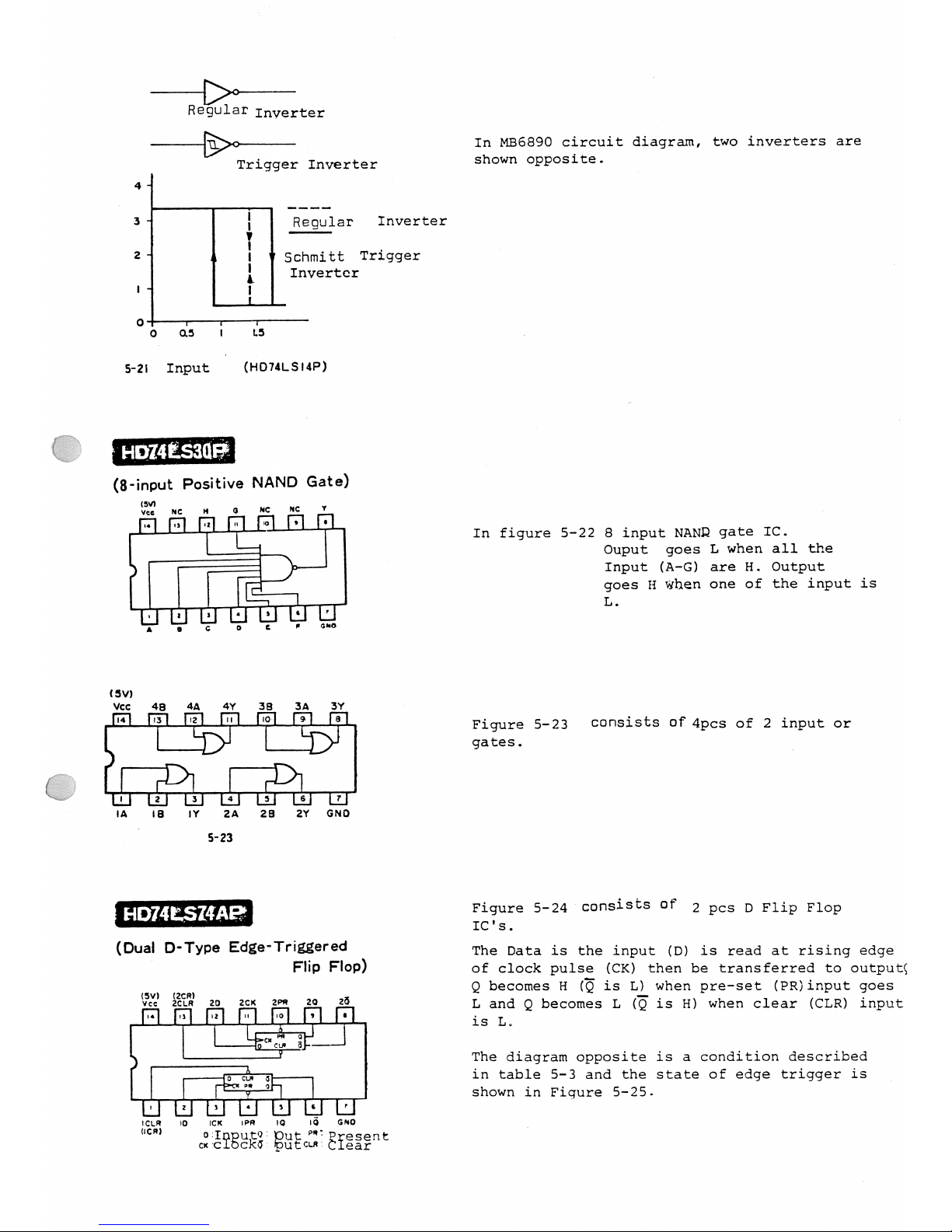
REQUl@f
Inverter
Trigger
Inverter
4
3
Regular
Inverter
2
Schmitt Trigger
Inverter
4
o
-r---
oas
u L5
5-2|
Input
(HD74LS|4P)
I
HDZ4ES3d§
(8-input
Positive
NAND Gate)
NC
pq
0
NC
NC
V
I
ll
D
I
I
ll
’il
K
GND
(SV)
VCC
4B
4A 4Y 38
3A 3Y
un
as nz
Il
IO
9 B
f ‘ i D 1 | i D 1
V!7\
Hn Hnnfr’
’TH V415|"f\
IA
ua
nv za aa av
cnc
’
s-23
E-lDT4|i$I4AE§
(Dual
D-Type
Edge-Triggered
Flip
Flop)
(SV) IZCR)
vee ZCLR
20
2c><
zvn
20
26
M’
.;
|;
ni
|o
9 |
cx ’f
cuvu
E I
li!
. ;
’.;J
*.;.’
’ . ; f ’ . ; i L ; . V
C33§T8E1%§:
$3527
EYSEEM
In
MB689O
circuit
diagram,
two inverters
are
shown
opposite.
In
figure
5-22 8
input
NAND
gate
IC.
Ouput goes
L
when all the
Input
(A-G)
are
H.
Output
goes
H when
one of the
input
is
L.
Figure
5-23
CUf"SiS’CS
of
4pcs
of 2
input
or
gates.
Figure
5-24
CDl’1Si5t5
of
2
pcs
D
Flip Flop
IC’s.
The Data
is
the
input
(D)
is
read
at
rising edge
then be
transferred
to
output;
when
pre-set
(PR)input goes
of
clock
pulse
(CK)
Q
becomes
H
(§
is
L)
L
and
Q
becomes
L
(5
is
H)
when
clear
(CLR)
input
is
L.
The
diagram
opposite
is a condition described
in
table
5-3
and
the state of
edge
trigger
is
shown in
Figure
5-25.
Page 27
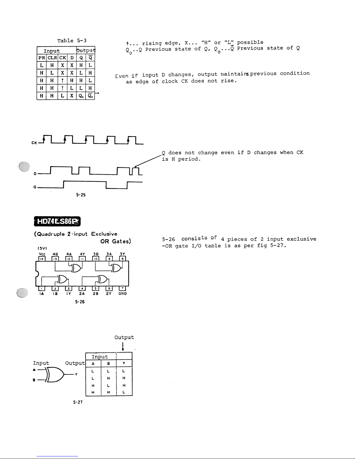
Table
5-3
EB IEIEIEI
EI III
I I I
I
l=
L
IEIIEI
LL
IIIIII
l1llIl
IIIIEI-B
Q~»
E
H
+I
H
H
+L
rising
edge,
X...
"H" or
"L"
possible
+...
Q
..Q
Previous
state
of
Q,
Qo...Q
Previous
state
of
Q
o
Even
if
input
D
changes,
output
maintainsprevious
condition
as
edge
of
clock
CK
does
not rise.
D
0
5-25
HDHESSSVEQ
(Quadruple
2-input
Exclusive
OR
Gates)
(SV)
Vcc
48
4A
4Y 38 3A
3Y
|4f
Lai
Ve;
?v|
Lo?is:
s
|
2
3
|4i
A5:
s
|1
IA
I8
IY 2A 2B ZY GND
S-25
Output
Input
Output
D D - Y
a
5-27
H
L
_
Input
|
L L
L
L
H
H~
H
L
H
H L
Q
does not
change
even if
D
changes
when CK
is H
period.
5-26
consiStS
OF
4
pieces
of 2
input
exclusive
-OR
gate
I/O
table
is as
per
fig
5-27.
Page 28
’
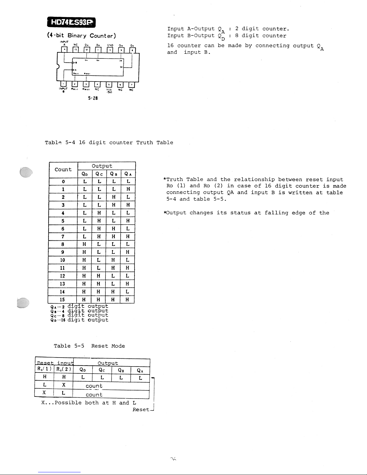
HD14IES93F!?
Input
A-Output
QA
: 2
digit
counter.
(4-mt
Bkmry
Counter)
Input
B-Output
QD
:
8
digit
counter
’NTT
0-
Gu
me
Q.
Q.
16
counter
can
be
made
by
connecting output
QA
I
n
I
B
H
and
input
B.
FQ
Q.
ua
Q.
EIIIIIIIIIIIIIIH
I
I
I
I
I
I
I
INPUT
Run
Run
NC
vcr:
NC
MQ
B
mv)
5-28
Table
5-4 16
digit
counter
Truth Table
O t
if
Cgunt
QD
Qc Qs QA
I
0
I
L
I
L
I
L
I
L
I
*Truth
Table
and
the
relationship
between
reset
input
l
1
|
L
I
L
L
H
’
Ro
(1)
and
Ro
(2)
in
case of 16
digit
counter is made
V
connecting
output
QA
and
input
B is
written at table
2
I
L L
_L
H L
5-4 and
table
5-5.
3
’
L
I
L
H H
4
1
L
I
H L
L
*Output
changes
its
status at
falling
edge
of
the
5
L
H
L
H
s L
H
H
L
L
7 L
H
I
H H
H
8
H L
H
L L
9
I
H L L
H
10
H
L
H L
H
I
H
L
H
H
I
N
12 H H L L
13
H
H L
H
14
H H H L
-
¢
H
»
H
¢
H
_
H
.
W
di it out ut
digit
outgut
Qc-_-5
digit
output
Qu~-~!5
digit output
Table 5-5 Reset
Mode
eseto
inpu
I
Out
ut
)QD’QCEIQBlQ,\
HHLILILIL
L
X
f=9vQt
count
R f1>IR
x
I
L
I
X...Possible both at H
and
I
Reset_1
’TQ
Page 29
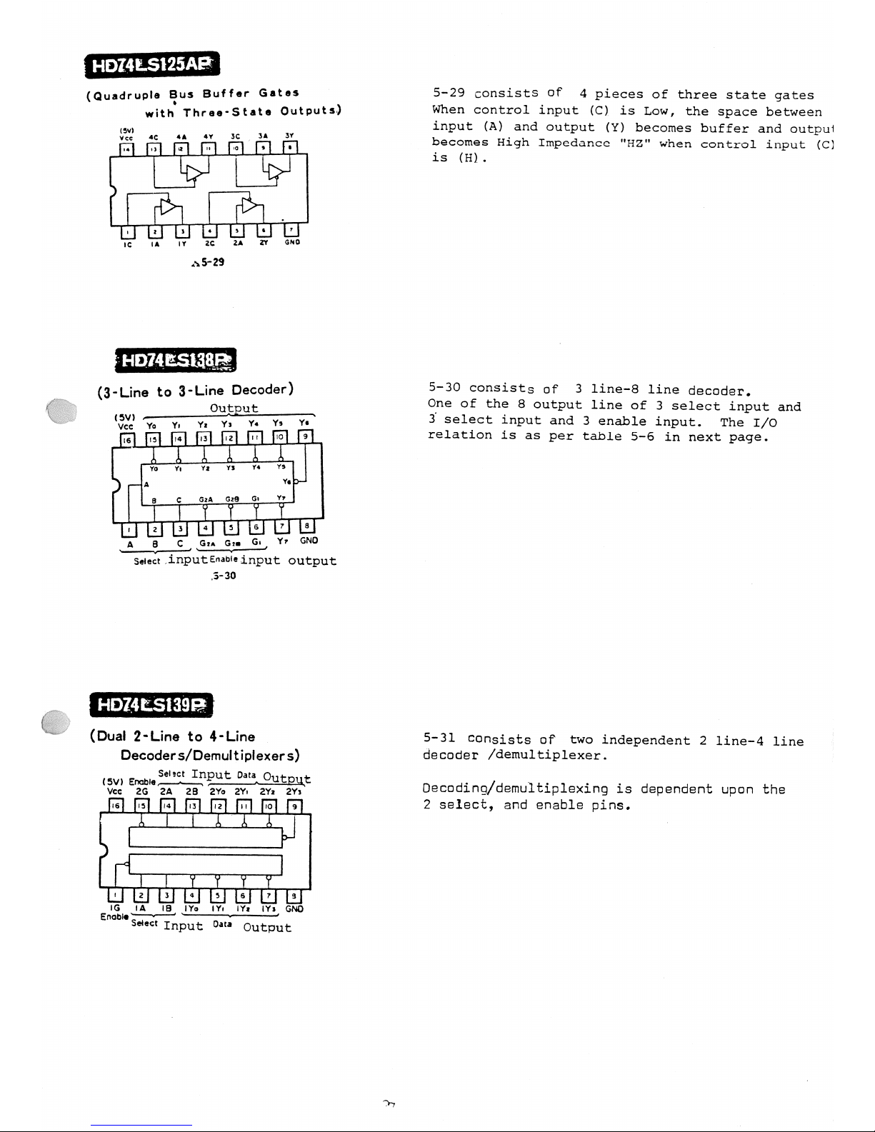
I-lDZ4E.S\
ZSAEP
(Quadruple
Bus
Buffer
Gates
5-29
Consists
Of
4
pieces
of
three
state
gates
with.
Three-State
Outputs()
When
control
input
(C)
is
Low,
the
space
between
(M
input
(A)
and
output
(Y)
becomes
buffer and
output
V"
" 3
" 3’
becomes
High
Impedance
"HZ"
when
control
input
(C)
U
U
EH’
U
’H
is
(H).
E
>
lik
lin
I
I
I
~
I
I
I
|¢
||
IV 2C
ZA
Z7
GNU
AS-29
=HD2=lE}Sl3§§_
(3_|__ine
tc,
3-Line
Decoder)
5-30
consists of
3
line-8
line
decoder,
Ougmt
One
of
the 8
output
line
of 3
select
input
and
(sv)
,
Y _
3
select
input
and
3
enable
input.
The
I/O
v
Y
,___ c. ._
_
t- e
i
~ - - -’ ’ ’ " "
relatlon
lS as
per
table
5-6
1n
next
page.
z
GB
Q YI
Yz
Yx
Ya
Ys
E
m
I3
|
Z
I ¢
O
9
vo
vu
YI
YI
Y*
Y
A
YI
5
Yr
3
C
G
A
.
1 2
B
B
6
8
A B
C
Gu
Gil
G*
Y’
GND
sem:
"input
Enabw
input
output
.3-30
Hnz-msiaseir
(Dual
2~Line to
4-Line
5-31
COF¢sists of
two
independent
2
line-4
line
Decoders/Demultiplexers)
GGCOUSP
/
Select
Input
D
t
Q
_
E ’ § § ’ ’ § ’ j § t
Decoding/demultiplexing
is
dependent
upon
the
,S
m
,4
,,
.2
,.
.O
9
2
select,
and
enable
pins.
IG IA
IB |Yu |Y| |Yz
lY|
GND
Enable?
ect
Input
Dan
Output
7"v
Page 30
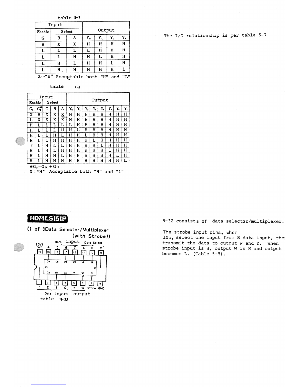
table
5’7
Input
Enable
Select
Output
G
B
A
Y,
Y.I
Y,
I
Y,
H
x
x
H
H
H
I
H
L
L
L
I
L
I
H
I
H
I
H
L
I-
H
I
H
I
L
I
H
I
H
L
H
L
I
H
I
H L
I
H
L
H_
H
_I
H
I
H
I
H
I
L
X--~"H"
Acceptable
both "H" and "L
t a . b l ‹
5_6
I I 1 1 D l . 1 t
Enablg
Select
_
Output
G, of
c
B A
Y,
Y, Y,IY.
Y.
Y. Y. Y,
x H x
x
XIH
H HIH H
H
H
H
L x
x x
X H
H
H
H
H
H
H
H
H
L
L L
L
L
IHJH
HI H
H H H
H L
L L
H
HTL
H H H
H
H H
IH
L
L
H
L
H HIL
H H
H H H
H L
L H
H H H H L
H
H
H H
1
L
H
L
L
H H
H H
L
H H
H
H
Hl L
HITTHIITIH
H H L
I H
I
H
H L
H H L
H H
IH
H H H L
H
H L
H H
H H
HIH
H H H H L
lG,=Gu
+
Gm
X
: H "
Acceptable
both "H"
and "L
HDNESISIP
(I
of
8Data
Selector/Multiplexer
(with
Strobe))
(sv)
I
Dafa*
inpult’
DutoASelect1
VCCQSSTABC
IS
B
I4
B
I2
| I
so
Wg
D4
Ds
Dc
Dr
A
3
D:
C
D2 Du
99 Y
W
5
___
’
1
2
3 4
5
s
7
3
3
2 I
o Y
w
sr}ooe
GND
ww
input
output
table
5
ll
The
I/O
relationship
is
per
table
5-7
5-32
consists
of
data
selector/multiplexer.
The strobe
input
pins,
when
low,
select one
input
from 8
data
input,
the:
transmit
the
data to
output
W and
Y.
When
strobe
input
is
H,
output
W
is H
and
output
becomes
L.
(Table
5-8).
Page 31

(Dual
4-Line
to
I-Line
Data
Selectors/Multiplexers)
I
can
Input
(SV)
Slrcbc Select
Cgyjgput
VCC 2G
A
2CJ 2Cx 2C|
2Co
as I5
’Id
H
I2
II
|o 9
I
I
ll!!
.
;"|
-
..|
I
B
1
4
5 s 1
a
»
IG Sdeci
IC: IC: ICI
lCo IY
GND
Sfmbt
B \
om
Input Output
-5- 33
’IT’1I>Ig_
:5-8
Input
I
Output
Select
Strobe
‘
" " 2 = " " § ’ T =
S
Y
W
X
X
X
H
L
H
L
_
L
_
L
I
L
I
ng
L
ng
I
L
L
I
H
I
L
‘
D,
I
D,
L
H
L
L
D,
I
D,
L
H
H
L
U,
D,
I
H
L
I
I..
‘
L
D,
D,
p
H
L
HI
I
L
D,
D,
I
H
H
I
L
L
I
D,
I
D. I
pp
H
H
H
I
L
’
D,
D,
X
:’H"
Acceptable
both "H" a n d " * L "
;I
eae
we
1/o
Truth
Table
(HD74Ls153P>
,Q
D
Input
I
Out
I
Salocf
I
Dqrq
I
gym"
,
aAcoIcIIc2
cs\
cs
I
Y
I
X
x
I
x
I
x
x
xx
H
I
L
L
L
L
I
x
x
I
x
L
I
L
L
L H
I
x
x
x
L H
I
ILIH
x I L I x I x L , _I . I ., I L. ._ I _. I __ I I ,
I
"
,"
I
"
I
"’
I
I
X
I
I-
I
I*
H
WL
I
x
x
L x
L
I
L
H
L
p
x
x
H
Dx
I
L
H
I
H
I
H
x
x
x
I
L
A
L
I
L
I
HI
H
x
x
xIYH
I
L
"
H
I
"
""
Acceptable
both H
and L g
OR
In ut
I
output
G
I
A
a
I
Y
I
H
I
x
x
I
L
’~
I
’~I’-
I
I
Value
of
Co
L
I
L
H
I
Value
of
Cf
I-
I
H
L
Value of
C2
L
I
n
I
H
I
Value
of
3
OR
by
other
expression
Co
Cx
-=>--Po
I,
Sw’
_
’
‘
Swz
cz-_-_.ee ~L
Cx
d
Yi
,
_,_
means
L
when
A
=
B
=‘L’,
connect a
When
’I
=‘L‘-
B
=‘H}
connect b
5
I1
C
G=’L’,
SW2
connect to X
When
A=‘H’.B=‘L,
connect
P
_H_
SW2
*=
connect to
Y
when
"=B=‘H}
connect
d
5-33
consists
UI’
2
pair
of
Multi-
plexers.
Multiplexer
is
the device which has
similar
function as
rotary
switch
which_take_s
out
necessary outpuii
(Table 5-9).
JDO
D-L-..
.--»-.U a n - I »
ll-UNI
|\|¢|ly .|.l||J\-I
MD
Page 32

HD74lLSl51FF
(Quadruple
2-Line
to
l-Line
Data
Selectors/MultiplexerS(Nonlnverted
Outputs))
Input
Cup
Input
Output
(SV)
,__ pl.1
_
__
VGC $ h & |
4A
48 4Y
3A
35
3Y
l5
B
I4
I3
nz ||
B
9
_-lm
B QA
48 4
34 53
5
’Iv
m m
q
u
n
Q
I
2
3 4
5
6
r
a
seeee
IA
as
_:Y
za
23
2?
GNO
Input
83%
Input
output
5-34
\
.5-I0
Input
Ioutpu
Strobe
I
Select
I
A
-I
B
I
y
I
H
X
X
X
L
I
L
L
I
L
I
X
I
L
I
L
L
_
IH
X
H
I
L
H
I
X
L
L
L
H
gp
X
H
H
X
Z ’ H
Acceptable
"H"
and
"L"
H014
ESISBEE
(Quadruple
2-Line
to
l-Line
Data
Selectors/Multiplexers(
lnver
t
ed
Outputs))
Innmollh
Imam;
output
csv: ,_f’-LPI-If ,-Z-.
Wx swam
4A
48
4Y
3A 36
3*
IBEEE IIIIEIB
338
I
.
¢;
4A
43
4Y
A
5
av
-
IA
IB
nv 2A ze
zv
.
.
I---i
_
»
2 5
4
H
6
T
0
Select
IA
IB
IY
ZA 26
2Y
GND
Input
03%
Input
Output
gas
5-ll
Input
IOutp
k
’Strobe Select
I
A B
I
Y
H
x
I
x x
I
H
L
I
L
I
L
I
x
I
H
L
I
L
I
H
I
X
I
L
JL
I
H
I
x
I
L
I
H
I
L
I
H
I
x
I
H
I
L
I
X;.H-
Acceptable
both
H
and
L
5-34
is
data
selector/multiplexer
which
select
one
data
from
two,
having
4
pairs
i
one
package.
Strobe
and
select
is
common
for
4
outputs.
When
strobe
input
is "H"
all the
output
becomes"LI
if
strobe
input
is
"L",
one
input
data is
selected
then
transmit
to
4
outputs
depending
on
the
state
4
select
input
from
2
input
signals.
The
selected
input
data is
transmit
to the
output
at
the
same
phase.
This is
the
data
selector/multiplexer
to
select one
data
from
two,
having
4
pairs
in
one
package.
The
strobe
and
select is
the
com on
for
4
output.
If
strobe
input
is
"H"
all the
output
is
"H"
If
"L",
one
input
data is
selected
and
transmitted to 4
output
depending
on
the
state of
select
input
from 2
input
signal
In
this
case,
selected
input
data is
transmitted
to the
output
with
reverse
phase.
Page 33

H
L
X X
XIX
H
H X
X X X
(4-Line
to
I6-Line
Decoder/Demulb
iplexer
with
Open
Collector
Output)
ww
VCC
A
B
C D
G:
Gr Oni
Ou
Ou Qu
Qu
EEEE BIEIIIBH EI
.
ABCD IS Z
0
I
"
IIBBIIEIB EIHIEUB
Go
Gu Cz Gu
Ga Gs
Qs
if
Ga C1
Cn
GND
5-35
s-I2 ’rrunh
Table
(HD14IS9P)
5-36
:
4
line-16
line
d9CgdEr_
Qutput
Q O Q 1 5
is
open collector.
Q
QJQtQJQnQ.QJ
L L
I
I
IUPUt
Output
G,G,D
c B A
Q.Q,Q,IQ1i Q¢
Q, Q.Q1Q. .
ILL
L LL
LLLL
LHI
L
L‘L
L
L‘H L
L
LLLLHH L‘
L L L H L L’
L
L L L H L H
L
L L L H H L L
L L L H H
H
L
L L H
L L L
V I I I I I I I I I
L
ruvvu
_IL-I"I’-I I"|||II|Jll|’~ lIlIIII
L H
Therefore,
G1=G2
=
L is
required
to
I
operate
decoder.
Lux. L
_
L
to
LLHLH‘H
L
LLYHHLL
I-I’
I
LLHHLH
Lo
LLHHHLI
I-
LLHHHH
IL
Lnxxxx
Either
of
G1
and
G2
is
"H",
the
output
becomes H
without
input
state
(A-D)
_
I
’Z
1
Page 34

SNZ4Sl
63l\£
(Synchronous
4-bit
Binary
Counter
(Synchronous
C|ear))
m
Output
(SV)
E n o m
VW
6¥
OA
08
Qc OD T
Load
U5
U5 Il
El
U!
ll Il
ll
§gg; ,G»
Ol
oc Oo r
ctw
LW
C*
A
B c
D
P
ll
ll
B
ll B
B
El
Clwf Clock A
B C
0
Emu. GND
om
input
P
5-37
Clsor
[__]
Load
[__]
A
’_t:::::"" ---~-----
om
8
:::::::;::::::;;1;:_;::::
Inputic
| ’ * " l " "
’
’----~----------_-_
_...|
I... ._._
-_
..._
__ ____ _
____
____
D
-----------..-.._...__.._-.._--
5-37
Synchronous
16
digit
counter
with
pxeset
function.
_This
counter
is
1
preset
programmable,
Preset
can
be
done
with
synchronization
with clock.
When
applying
"L"
to the orad
input,
data
is
outputted
which
shoul
be matched
with
input
data
at
next
clock;
pulse
regardless
enable
input
level.
Clock
Enable?
’
’
_ _
I
p
Enom,
.
I
’
Lock
function is
synchronous
with the C § i C 3 C i §
I
n |
»
,./
_
_____
’
and
if the clock
input
J.S"L’;
each
flip
"1
|
I
QA
_____
_+
,
V]
Q
f-LL
as
||
O
_
____
_ _
,
,
output
becomes L
at
next clock.
B______
|
Outpu
o c _ _ _ _ _ _ _ _
:
I
jjj-
In
this
case,
it
has no relation
which
---:T
§
’
input
level.
Curry
;
f
1
|
l
i
I2 I3 IA
I5 0 |
2|
I
i
i ;C U"’i-L-lnnioaf
Clear
Preul
5-38
Page 35

I-IDZ4ESI64F!¥
(8-bar
Parallel-our Shift
5-39
consists
of an
B
hit
parallel
output
Regster)
shift
register.
Q2
El2f§§§i_____
mm (3,
IN
serial
input
A
and
B
,
internal
gates
are
,_l
1;
f;
’
U
included.
Therefore,
if
either
of
the
input
is
"L"
during
the
processincx
data,
new
data
Q
M M M
cy
input
is
prohibited.
Cx
, Q
Q Q
__
Clear
input
is
not
Synchronous
and
the
data
is
shifted
at
the
~
2 1
.
, ,
l,
rising
dege
of
the
clock
pulse.
~;V_B.,m
m
_W
m_
W0
The
time
chart
is
in
5-LO
and
1 H P u t _ _
Output
the
function
table,
in
5-13.
5-39
Clear
L_’
.A
L]
_
Seri.a|_
I
V1
:
input
’
}
_B
,
:
Clock
|
,
I
---4
~
r-1
=
QB
; 1 _ _
F11
;
Qc
1:13 |’_\ r-1
:
Oo
" "
5
output
If,
| |
I
|
f
os
___J
Q=
1:11
;
Oc
" ’]
~
II] r-t
,‘
*_*
swtiming
~(HDMLSm4P)
Table5-13~
(HD74L.SI64P)
7*
71
|
bfi
ff
Clear
i
Clock A
B
QA
Q B
...._.___
Q"
_
L X X X
L L
L
H
T
H
I
H H
*QM
-..... ...
Qc-
H
I
T
I’
i
X
L
QA-"‘
Qc.
H
I
T
X
I
L
Q
L
R
QA!
""""‘
I
Qc.
? = , = L ’ = ~ . H ’
D A S
A A A " "
-
" I.
C
\,u5\:
» . , l , ¢ , - - , _ i G . . .
L‘,L,,;.V
_
X"’L
OT
H
accept
condition of
Q
QL.
4 X
Page 36

SNUESIGBEE3
(8-bit
Parallel/Serial
Input
Serial
Output
Shift’
Register)
(S/L)
15v1smn
(Cm
Vcc
Load
H
On
G
F
E
Cleo?
I6
715
I4 I3
12
ll
IO
9
srwv
14
Q..
G
F
E
Load
Senal
Input
Cho#
Clock
gp(
A
a
c
u Innubil
,
, 2
3
4 5
s
7
a
5¢f1a1 A a
c
0
Clock
Clock
ow
Input
Inhibit
(CK)
(son
lg"
5"4I
CK
5-41
Synchronized
parallel
load
8
bit shift
register
can select
2 states.
Serial
shift
from
serial
input
(SI)
to
output
QH.
Shift
the
data
from
H
to
QH
in order
in
parrallel
input
(A-H).
Having
two
inputs
of
(A-H)
and
serial
(SI),
parrallel
input
one
output
belongs
to serial
output
QH
when shift
load
(S/L)=H,
serial
input
(SI)
becomes
possible.
This
input
is shifted
to
QH by
clock
pulse.
Parallel
input
(A-H)
becomes
possible
when
shift/load
(S/L)=L.
In this
case,
Parrallel
input
(A-H)
is
loaded
with first
clock.
This clock
is
loaded
with
first
clock.
This clock
is
synchronizing
with
parrallel
inputs.
Then,
input
is shifted
by
1
load,
period,
when
not
shift,
and
if
L
(CR)
is
independently
rising
edge
of
clock.
clock
A-H
to
QH
in
order
(during
clock
inhibit
(CI)=I-I,
clock
will
level,
shift
can
be
done.
Clear
valid
when CRFH
shift
is done
at
cx|n11a»11
’I
{
1
| ’ * " ]
Q
Clear
_LJ
f
f
Seria|3: Q
3 :
Q
sr1.f1/tm
’f
1 ’|
E
A
-1
3
Q
I’
1’
’
L
!
1
1
1
C
-1
1
§
|»
1|
1
5
1
1
1
Pm11¢1Out
uqc’i
5
O
5
i
E
-4 1
2
|’1|
1
i
1
F
-1
i
i f
i
.lE5VAT’1J2
.l
E
5
VAT’
1
J
2
H_I 5
5
F f ’ 1 l
¥
3
~I3!
F1
ri ; - L i I ~ 1 L 1 » L _ _ r ~ 1 _
1
I 1 I ]
I
Se’a1 Sh‘f|
= ;
p
:g
‘ ’ "
_--
V
CR
f 1
Loiilnmw
{<
Senal
Sum
5-42
Time
Chart
(SNHLSISSP)
I - | D Z 4 £ S E 1 4 E ?
‘
D
t
Edg
Triagered
¢ ‹
9’
.
_
.
(Hex
Fry
=-’ops
with
Clear)
5-43 consists
of 6
piece
D
Flip
Flop.I/O
xp
.
wx)
relation
is shown
at
table
5-14.
This
table
ax
gg
so
so
50
40
40
ann
shows
the same
one of
HD74LS74AP
I/O
Relation
,6\
,,
[Ml
,,
15
H
IO
9
Table
except preset
(PS).
The
I/O
Timechart
»
V
5
’
is the
same
as
HD74LS74AP
o
u
0
cts
U,
CU’
cn
ctn
Q,
_
Q
§
’
’
11
’
z
1
4
5
5
7
fj
1
Cm:
IQ
ID
2D
20
30
30
GND
ZCR)
"/
Du
Page 37

S-I4
i
Clear
‘c|¢¢k
D
Q
Q
L
X
X
i
1-
H
H
T
H
|
H
L
H
T
I-
I-
f
H
L
X
Qu
Q0
H D I 4 E S H 5 F ! -
(Quadruple
D-tl/535
Ed3e’T"ig3 ’ed
Fiip
Flops
with Clear)
(SV) _
"
sq
(gg
Vcc
40
40
4
3
3
|5’
15
as
[is
*Z
"
O
9
~
*
.
\ 2
3
5
6
1
G.,
,Q
16
no
zo
25
zo
sno
(cm
5-44
V
SNI4ES245Ni
(Hex
Bus
Drivers
and
Receivers
with
Three-State
Outputs)
C q d ( m R )
Function
L
L
H § L c ~ ’ A g H t
I
Enable
Direction
I
L
H
A?
»BO¥1§
ut
EP
I
I
H
I
X
LHigh
Imped
nce
x".Accept
both
H
and L
(SV)
Vcc
Encbln
G ai
In
HD74LS174P,
Q
output
does
not
exist.
X...Acceptable
both H
and
L.
+...Rising
edge.
_
Qo,
Qo...Previous status
of
Q,
§.
5-Ala
consists of
a
lines
Flip
Flop.
Difference
betweer
HD74LS1Z§P
and
this
chip
is
the
existence
of
reverse
output
Q
pin.
The
I/O
relation
and
time
chart is
the
same
as
HD74LSl74P.
5-45
Consistsof
Bi-directional
bus
buffer
(8
input/
output).
By
enable
input
(Ei
Low
and
setting
direction
control
(DIR)
signal
transfer
direction
A+B
is
switched
to
B+A.
When
enable
input
(Ødis
high,
no
signal
communication
between A
and
B
is
done
and
keepsthree
state
High
Impedance.
\= l
I9 IB
V
V
AA
az
as
B4 as
as
37
as
|7
¢§ |5
M I3
IZ
H
I I I I Y
l
GND
i
v
v
v
i
-L I
W i
I
|||
:Za
43| »44 |5\
Q61 |71 L81 i9\ P01
Al
A2 A3
A4
A5
A6
A7
A6
DIR
5-45
Page 38

ABA1-zzz
HD74§525ZE§
(Quadruple
2-Line
to
I-Line
Data
Selectors/Multiplexers
(with
Noninverted
Three-State
Outputs))
uw
v¢¢?:‘Sf» rf‘f=I4A
48 4Y
SA sa av
ue
us
m
I3 I2
||
m
9
--__-
oc
an
as
4V
JA 38
5
n
IA ua
nv
ZA
2B
v
§11__
1
2
3
fi* *S
7
v5
som IA na
Iv ZA ze zv GND
5-46
546
In ut
Output
oc
|
s
A
B
H
x
I
x
X
I
Z
f
L
L
I
L
x
L
L
L
I
H
I
x
H
L
H
I
x
L
L
H
L
H
x
H
I
X
;
-Kclcept
e
botlH and
L
Z;
High
Impedance
(OFF)
H D Z 4 E $ » 2 8 3 E ‹
(4-bit
Binary
Full
Adder)
( 5V)
vtc
BJ
A3
Is
A4 B4
Z4
C4
Data
Selectors/Multiplexers
with
three
State
outputs
Inputs
consist
from 2
data
(A,B)
which
decide
status
of
each
output
and
select,
output
control
which
are
common
for 4
outputs.
When
output
control
is
H,
all the
outputs
go
High
Impedance,
and
when
L,
output
the
status
data B
if
select is
H.
If
select
is
L,
output
the
status
of
data
A.
4
bit adder. Each bit
sum is
obtained
by
the
B
m B B
B
m
m E
Z
output.
The
signal
from
4
bit
output
or
more
higher
bit
can be
obtained at
CL#
output.
Bs
AJ 2|
44 B4
I*
I:
C*
B1
It
2|
M 3*
5
| _ in
_3_
‘4_ >5_
767
S
E2 B2
A2 2|
Al
Br
CO-
GND
S-47
547
Sma:
Out ut
C.:-Lo
C = ¢ H l
Input
c=l_]§_n Ctshgn
The
input
condition
of
Al, Bl,
AZ,
B2,
and
CO
is
’
used to
decide the
El, Z2
and
internal
carrier
C2
c2z’%:
2
A. B,
A.
B. Z, Z. C.
EJ
L
L
L L L L L
H
H
L L
L
H
L L L
LIH
L
LVHpL
L
L
H
H
L
L
L H
L
H
L
L
H
L L H L H
H
L
H L H H
L L
LHHILHHLL
HiHHLLLHH
I I I I I I I 1
~
1
L
|
L
|
H
|
L
|
H
|L1
H
HLLHHH
LL
L
H
L H
H H
L
L
HHLHILLH_H
L
L
H
HILKL
H’
W _H
HLHHHLHL
I
LHIHHHLHL
I
HIHr"HIHII.IHIHIYH_
value.
The
value of
CZ,
A3,
B3,
A4
and
B4
is
used to
decide
Page 39

% .
(
~.‘_,_
HDZ4ES36Z’AE§
(Hex
Bus
Drivers
with
Three-
State
Outputs)
V
5-48 consists
of e
6
piece
bus
driver with
tri-state
outpi
eg
E’
SA
sy
SA
ST M
Y
6
gates
are combined to
4
pieces
each__and
2
pieces
..
., ..
Q,
’Q
H
U
_
then connected
to control
input
(G1, G2).
when
control
input
(G1,
G2)
is
low,
the
space output
(Y)
becomes buffer
and when it is
H,
between
input
(A)
and
output
(Y)
goes High
Impedance
"HZ".
I
2
3 Q
5
¢
,
.
El
IA
IY
ZA
21’
3A
’BY
Guo
5-48
HD75I08AE¥
(Dual
Line
Receivers)
vØbvl
v¢Ø 5V)n B1
Nc
Y, G,
E B I
I
I
U
T
B
’
J
:ell
n
B E u
B U
n
5-49
CO;-,siggs
Of*
2
pairs
of
Line
Receivers.
Aa
Bu NC
vu
Ge
5 GMI
.
+
5-49
Power
is
-15V
two
supply.
when
op
input
(A-B)
is
548
more
than
25mV
amplitude,
TTL
compatible
logic
level
_
Strobe Gut
signals
are
outputted.
put
V|ND=A’-B
G
Y
S
Y
vmzzsmv
1
x
I
x
H
X L
H
-2smvzsmv III
zsmv
III
l..l U
f
ll
1 ll;
A
x
L
H
vm;-zsmv
H
|
H
H L
X-~
Accept
both H
and
L.
,_HDZ5188l?=
(Quadruple
Line
Driver
5)
(Iva)
4
4A 4Y 3B
3A
sv
\’ l
\
5-50
C O V I S 5 - S C SOf
4
pieces
line recØiver
NAND
Gates.
Difierence
from
HD74 Series
is that
the IC
operates
JM 5-jx-\
using
:L-12
v
and
not
5\/,
whir:h_satisfies
the condition
l
H
[Ll
|
required
for
the RSZEZC
interface.
ill
2
H
1
4 5
s
’rf
-v=¢
m
uv
2A
ze
zv
Guo
(-|2V\
5-50
37
Page 40

,»
t
(Quadrupre
Line
Receivers)
5-51 consists
of
A
Schmitt
trigger inverters,
(5V) control
Contrql
each
with
a
line
receiver control
input.. By
Vx
4A 4
4,
BA
3
BY
connectlnq
reslstance to control
lnput pln, lnput
m
[Fl
I
thresh-hold
voltage
can be
changed.
4
2 3 4
5
W
lr.
IA
cPntrol2AcontrQ!
G~g
2
$5|
vcc
W)
2K
5 V )
I
V
.
Y
4‘
""
Jntrol
input
input_
A
""
S
lin
’GND
&S2 Circuit
C
’I;iming
resistence
connection
1
,
|
Tir‘ng
capacitor
connection
~
(+5w
NC
NC
NC
NC +ve:
E1 El
El El
B El
Pha e
21
EXE
Det
Ctor
El
n
u u n
-wr
lHDUtVCOOUE
V60
control
voltage
hsvv
T
pu
.
_
1
Standard
Output
(Reference)
Phase
Comparator
VCO
Input
5-53
5-53
Consists of
3
Blocks
1. Phase
Detector
2. VCO
(Voltage
Controlled
Oscillator)
3.
AMP
:
Amplifier
YQ
Page 41

6 _
STRUCTURE
E16-l
Shown
at
figure
6-l
is
MB-6890’s block
diagram.
The circuit
structure
is
explained
as
below.
f
"
"_;’
il
’T
|
1"
H
»
|
Mpu
, |
F a
6809
EXTAL
e
Clock
I
__
g
nerator
NMI
TE
I
f":""’;"_| J -_.. ! I
Trace
_G?§¢
=
|
| _
’
Counte-
’u
e
_J
Timing signal
|"""’_
Generate
block
T
pi
CRTC
_
1
1
..
Mm.
l
ll
g
,
r
’
~‘
I I
W
E
ol
L___
.
_
~
-
ia
,_-.___-_---.---1. ,
1
I
’
n
;
i
Agdr
7
Li
ht
Li
t
es-
T
~
.
_
gggnecti
I-
|
Øweeai
|
_
_
_
_
e
I
{BREAK|
-1
RAM
I
|
0 0
BLOCK
.
M
’
Keyboar
ll-
I
|
_I
T
’
|
Cassatt
Acm
,
olour
I
Ho4ea5oP
bill!!
I
egiste
|___
_
ideo
D
,
A
||
I
.ØggiØfor
C3558
t s-zszc
|
OC
Pecorve
,,F
T
|
VF
A
|
ll
I
s c
B
I
‘
gggØgggiq
Ølsoiilgfection
U
!
E
"’eri
‘ ’
"o‘our ’Corr
o
i"e
!
e § e C % l n
S
I
araiØel
iØeo
siggai
Princ r
I
OW
C an
e
eneliØto
ge
erat
r
’
‘
PIA
_
gngggg o driv
Ho4ee2|P
,i
gg
|
_
_F
__}
L.
._.._.._._._._
__._......
’........
.
ak;
V
Sneaker
Q
giharacter
@
generator
Colour
Monochrome
U)
»
.
§§\%uiEic
3
Display
Signal
Generator
pp
_
M
Graph
Generator
Expansion
lTerminal
Figure
6-1
MBGBQO Block
Diagram
39
Page 42

[one of page 40-44 missing]
Page 43

1.
MPU
Peripheral
Cirucit
MPU
operatesby
EXTAL
signal
(4.032MCK)
which is
supplied
by
timing
signal
generator.
The
Address
signal
of MPU
is
supplied
to
CRTC, ROM,
RAM,
key-
board
peripheral
circuit,
extension
terminal
through
address
buffer
and
data
bus is
connegted
to
RAM
expansion
terminal
and
expansion
terminal
through
buffer NMI
pin
is
used
to BREAK
interrupt
from
trace
counter and
keyboard.
Eid
pin
is used
to
detect
input
of the
keyboard
and
FIRQ pin
is
for
Timer
interrupt. By
applying
Low
level
signal
from
outside
to
DMA/BREQ,
MPU
operation
stops
temporarily
address
bus
and
data
bus
is
separated
from
MPU in
this
period.
2.
Timing
Signal
Generator
System
signals
are
generated
in
clock
generator
by
dividing
32,
256
MHZ
clock
pulse
from
crystal
oscillator,
16.128
MHZ,
8.064
MHZ,
4.032
MHZ
and
2.016 MHZ
clock
pulse
are
obtained. From
these,
16.128
MHZ
is
for
timing
signal
generator
and
4.032 MHZ
is
for
the
EXTAL
signal
to
MPU
and
Video
Signal
Gerneration.
By
the
E
signal
(l.OO8
MHZ)
outputted
by_MPU
and
system
signal
generated
output
clock
pulse
(l6.l28
MHZ),
RAS
CAS
signals
are
generated.
These
two
signals
are
used
for RAM
driving purpose.
At
the
same
time,
CHRCK
signal
is
outputted
from
system
signal
generator
to
CRTC
(This
signal
is
master
clock)
by
this
signal.
CRTC
generates
the
Address
(MA,RA)
signals,
Horizontal
and
vertical
synchronise
signals
and
cursor
display
signals
and
bridge
the
data
between
MPU.
3.
RAM
Block
RAM
block
consist of
32KB=l6KBxl6
Programme,.
Store RAM
and
l6KBx5
Colour
Store
RAM.
Colour RAM
and
Program
RAM
occupy
the
same
address,
therefore,
the
signal
receipt
and
sending
between
colour
RAM
and
MPU
is
done
through
colour
register
.
4.
Video
Signal
Generator
Program
RAM
data is
outputted
from
character
generator
or
graphic
generator
as a
parallel
signals,
then
converted
to
serial
signals.
After this
con-
version,
these
serial
signals
are
mixed
with
the
colour
signals
from
colour
RAM,
thereby
making
seperate
colour
video
signals,
which
are
supplied
to
the
colour
display.
On
the
other
hand,
separate
colour
video
signal
becomes
monochrome
video
signal
by
monochrome
mixture
video
signal
generator
circuit,
then
is
Supplied
to
monochrome
display.
5.
Keyboard
MB-6890
use
the
hardware
scan
method.
This
method
is
done
by
counting
hori-
zontal
synchronize
signal
and
their
equal
frequency
HP
signal,
then
scanning
decoder
IC86
:
HD74l59P
output
and
multiplexer
(IC9O
:
HD74LSl5lP)
input.
By
this
scanningL_we
can
detect
the
input
from
the
keyboard.
By
detecting
keyboard
input,
IRQ
interrupt
is
generated
to
MPU.
By
this
interrupt,
soft-
ware
procedure
is
done
by
IRQ process
subrutine.‘
Also,
E56
interrupt
method
make
the
keyboard
input possible
even
if
other
data
procedure
is
under the
way.
Page 44

6. Cassette
SAVE
Load
Circuit
Cassette SAVE
circuit convert
the
data
signal
from MPU to
serial
signals
by
ACIA
(Asynchronous
Communications Interface
Adaptor).
This
signal
is
converted
to FSK
(Frequency
Shift
Keying) signals by
the
1.2 KHZ
and
2.4 KHZ
signals
which
are
generated by
dividing
E
signal,
then
outputted
to SAVE
signal
of the Cassette
Recorder.
Cassette Load
Circuit
convert
the
played
signals
from
Analogue
signal
to
digital
signal, by
PLL
Circuit,
also convert from
serial
signal
to
parallel
signal by
ACIA then
outputted
to
MPU data bus.
7. RS232C
Interface
Circuit
In
RS232C
Interface
Circuit,
l6.l28 MHZ
clock
divider
generates
the
receive/send
baud
rate,
and
Sends
this
Signal
to ACIA as
recieve/send
clock.
In
case or
sending,
according
to the
set
baud
rate,
the
data
signals
from
MPU is sent
by
converting
to
serial
signals,
and
v i S @ V @ f S @ »
in
case of the
receiving,
recieved
serial
signals
are converted
by
ACIA and
outputted
to
data bus of
MPU.
8.
Light
Pen
Interface
In
the
Light
Pen Interface
Block,
when
light pen
is
ON,
this
is
detected
by
IRQ interrupt
then
inputsthe pen
location
signal
(LP
STB)
to CRTC
(CRT
Controller).
9.
Acoustic
Output
Circuit
The
acoustic
output
circuit
uses
the
class
E
push/pull
method,
and
is
used
for the
keyboard
input
Click sound
and
beep.
Page 45

(I)D|PSW
&l Internal
Register
Structure
’Addres
Register
Data
Fit
1
R/W
i
FuI1CtilO1T1
Circflit
Name
D, D.
D, D. D,
D, D,
D,
READ wam-:
No
H
sFFcx 6%
BK
Q
><
BK=-x’,.i
anmx Nm
|lC98
sr-*Pcs BBW
D, D.
D,
D; D,
D,
D.
D,
0
><
1 1 s ? i ‹ § t § v r { f \ 1 I \ C t i O 1 l \ f g ; ;
f\1I\CtiO1l\fg;;
SFFCA
?5E§
T
O
X
g&§?}
Timer1RQ
lxcm
srfrca EEE
LP
O
><
Fgigx’
L/PEN
mo
IC24
SFFDO §6 .’ w
HR
1
c
\ClB
as
BB
><
0 Table
6-2
mas
1
sF1=Dx
’WEE
1
f>M1xIO tracecountelzcu1
M
1
x
I
O
trace countelzcu
1
SFFD2
@6175
’RM
F
n
><
0
§§3131’,re1ay
ON
xcxzs
1
s r ~ 1 = D s
TfT5§?i
Ms
><
><
0
rcs:
SFFD4 1TITT¥1?\§E
‘
TM
><
><
0
l;§’§I?1
:cu
1
s m - D s
EFESET
LE
1
><
0
W L ; E 9 1 , § %
_
rcz4
SFFN
iii§EEEEEE
11
I Ars
x
1
C)
§j%§§g;§§%§§i;§2dØuuw1
SFFD8
KETEEETQE
’mx
1
i
’cc RV,
G R
I
D
1
0
0
Tablel16-sl
1
:_
BMISS
Us sr.
HR KN
Q
Table 6-4
Iggy
"Fm
KB
l
D, D.
D,
D.
D,
iD, D.
Do
0
1
mga
I
The
DIPSW
register
to set
initial
condition of
only.
When
Power is
ON.
6-3
Address
0200593
Block’
6-3-1.
Internal
Resistor
Structure
In
basic
Master
L-3,
above
hardware
registers
are
incorporated
_tDachieve
the
various
functions.
The
functions
of the
main
registers
GTE
GS
explained
already.
the
Basic
language
read
Mode Bel
As
shown in
Table
6-2,
the
write
only register
is used to
set number
of
display
character/graphic
mode;
cassette/Rs232C;
and
background
colour.
Table
ez
MODE SEL
Register
Function
w
;HRH_
Made
_GB;RB_13B
1 : f ’ & Ø ; i § 7 . » U 6 : p u
1
0
E0
b h ,
Hiqh
Resolut‘
n
O
0»
0
Black
oi
1|
4&h,
Normal
0
9 1
~B1;e
1;
od
8@h,
High
Resoluti
n
O
.1
lo
R;genEØ
1
’ 1 l U 8 & : h , N o r m a I
011 3
1
0 0
Green
1
C
1
Mode
1
o
1
Cyan
‘
0
f
Cassette
1 1
»0
Yellow
?
|
1
as-2325
1
1_1
1
I
1
Lwmte
1
Page 46

6 2.
MPU
6-2
IC6
sN74Ls245N
RAM3,RAM4’
Connector
- gufgf
HDGBOQP/MCSSOQL
IC7
IC9
|f4~vPs:
U
"
" " " ’ " "
"
74Ls367AP
R0MJMM.W&AmLcRmet¢
AavAa»|F4~oF5;
Connector
ABQ-’A8\3>RAM
+5V1cz4
zc2z+5V
ddress
u
BOMB
-
-e>
»-
Qus
me
2’
Jcm
1/F1~4/F6
+
5 EE
A
~A|5
ddres
KSNMU
ENiMousse.
EN
i
Mousse.
’/F~1’~’/F~6
*Sv
HALT
QECDEfE‘1"f"T
IC9
* " ~ Y
wa-
at
--»
A
.___
+ s v J , " " T -
Zsll
=
v ~ = @ f 9
_
Qfxggi
|/f.’.1_VF5
§
EW
Address
,cn
+
74’-SOS"
Decoder
74Lso5P
EV
gggger
1
M
R/W
>
C?/W
||c24
|c24
74|_sosP
74LS125AP
+5V
I/F»1-1/Fs»~{
__
E
E T
FWO
IC41
rcgz
‘
74LS367AP
1
GZ’
I
Q
_
IC2
W
-
’
T
7 4 | _ s 3 e / A P
I
IC95
’
,
EXTAL
W I
_I/F5
4.o32MH=.
5 2
MPU Circuit
1.
Data Bus
Do-D7
(Bi-Directional) ,
which are
directly
connected
to
ROM,
RAM,
PIA,
ACIA and
CRTC,
conducting
the
receipt
and
sending
of the
data
to MPU.
Through
IC6,
these data
bus
signals
also
conducts
the
transaction
of
the data between
system
expansion
connector
I/F-l-I/F-6,
memory expansion
connector
RAM
3,
RAM
4 and MPU data bus.
6-2 MPU Circuit
Figure
6-2
shows the MPU circuit.
In
CRTC,
the location
of the
light pen
is connected to
the screen
address information
then
outputted
to
MPU
through
CRTC data bus.
Page 47

Table
s-3
c-neo-sen.
Register
function
MK
Mo
es
GC.
Mode
RV
Meds
ic
R B
QØigiki?-Y
I _i
&¥§§;?
I
I
0
gCharacteq
t
Uanormali
O
0 0
Black
1
&
1
rite
s’
Graphic
1
everse
Q
0 1
Blue
0
I 0
Red
0
1 1
Magenta
1 i0
0
Green
1 0 1
Cyan
1 1 0
Yellow
1 1 1
White
Table
&4
Register
function
--- U
’
| 1 r n
BM
I Mode
i
55
H
Mode
i
Sl. HR
KN
|
Function
K B N M 1 P r ? h ’ b i
0
I
KBIRQProhi
i
o o o
YSHIFTIA
Mode
’LED
ON
0 0
|
1
I
h 9 7 J 7 ’ L M O d e - L E D
ou
UE
U
Mode
g
0
en
e
Op
U
1
pro
1 it
2)
3. C-REG-SEL
As shown
in table
6-3.
Read/Write
information
registers
to
RAM
(IC64-IC68).
6-3-2
Address
Decoder
Circuit
Address
Decoder
circuit
is
divided to
3 circuits
depending
on address
area
which
is
decoder
as
follows:
(1)
ROM
Address
Decoder-
Allocated
address
of
IC2-ICS
is shown
at table
6-5.
When
address
each
ROM,
ROM
Address
Decoder
circuit
supply
L level
signal
to
each ROM
20
pin
(Chip
Select
Pin).
Fig
6-3 describes
the
main circuit.
In
the
decoder
circuit
shown at
figure
6-3,
Input
of
ICII
has
upper
3
bit
AB15, AB14,
AB13
of
the
address
bus are connected.
At the
Output
YO-Y3
of
ICII,
L level
signal
is
outputted
as
the block
of
$2,000
address
from
address
$8,000.
When ROM
mask
signal
ROMKIL
is
H
level,
dsssds
signals
are
outputted
as
per
the
allocated
address
in
Table
6-5
(below),
to
20
pin
of
IC2-ICQ.
These
ROM IL
signals
comes
from
system
expansion
connector
and RAM
expansion
connector.
At
pin
number
20 of
IC5,
address
d e C O d e r
signal
is
outputted
after
getting
ri
of
Sygtem
I/Q
addregg
($ppQQ~$FFEF)
from
internal
register
by
IC33
(2)
System
I/0
address
dgggdgr,
circuit.
This circuit
dsssdsrthe
system
I/O
register
(SFFOO-SFFEF)
which is internal
register
address.
Main
circuit
is
shown at
Figure
6-4.
As shown
dsssdsr
circuit
in
Figure
6-4,
input
of
ICl2
has
upper
13 bit
addregg
bus
gf
A315-A33
are
connected,
L Level
signal
is out-
putted
as
a
$8
address
block from the address
SFFCO,
(Table
6-6).
Further,
this
signal
is
decoded.
by
lower
3 bit
address
of
AB2-ABO
in
ICII and
ICl3,
generatesthe
address
dccodØ
signal
which corres-
pond
to each
system
I/O
address.
4
5
Page 48

(3)
RAM
address
decoder
circuit
This
circuit
decode
the allocated address of RAM
and
RAM
expansion
connectors
The
circuit
diagram
is shown at
Figure
6-5. In the
circuit
shown at
Figure
6
standard
incorporated
RAM address is
decoded
by
the address
bus
upper
2
bit
(AB15-ABM)
of
IC33.
Thesetare
outputted
as RAM 2
SEL
signal,
L
level at
the
address
of
$4000-$7FFF
and as RAM l
SEL
signal,
L
level
at the
address
$000-$3FFF.
The
address
signal
which
is
outputted
to the RAM
extension
connector
in
the main unit is also decorded
by
ICl37.
The
upper
5 bit
AB15-A1311
of
the
address
bus
is
inputted
in
ICl37,
and
output
of
ICl37, ILYO-1Y2,
ZYO-2Y,
are
outputted
to the
RAM
expansion
con-
nectors mhich
correspond
with the
address shown
table
6-7.
Therefore,
in
case of
expansion
the
RAM,
no
further address
decording
circuit is
required.
Table
6-5 ROM
Allocated
Address
A
ROMITE*
I
ggi?
{ E u n c t i o n
IC2
---""‘
Ssooo
SQFFF
I
BASIC
Expansion
{C3
~PI>z3s4c~3so
Saooo
SBFFF
i
EASIC
A
’
gIC4
,uPD2364C-331
Scooo
SDFFF
[BASIC
ICS
~Po2ss4c-332
S5000
"EFF
| s B § § I C
SFFFO
SFFFF
[Monitor
A6
Page 49

ICIBB
]C2|
g : § § ‹ § § , I c 1
now x
:_
,>0,
141.s1a9P
MI
|1025
Q
|
m,
-
.>
-.
>
fcziv
PJ-U
A813
A
IC29
.V
’cm
Pin
nam
na
2
ICZ9
,,,
»
.
new
pin
.IICZS
’IC26
:ie
;
-
»
~
Pin
When
5FFoo~$r-’Far
1c33
’H’
Level
Fig.
5~3 RSM
Address
Decoder
Circuit Main Parts
|¢3Q
IC12
14|_S3op
74LS138P
!N
LSI-SE
when sF»=o0~sf=z=rr=
Y
L
L L e v e 1 A B
A
Yu
~
A84
5
Y2
~
ABQ
A B
C
Y:
_
ABS
5
Y
l-
4
*
9
:cans
G
Ye
-
ABIS
#Br
5-
m Y,
.
Fig.
5-4
System
I/O
Address
Decoder Main Parts
Table
6-6
ICIZQ
Decode
Address
.I
YFDEQCOCIE
AddreSS‘
S
.
1.
Y
f
_
*
res?
Decode
lgna
S
Y
~
;FFC
SFFC7
Table
6-7
HAM
expanslon
connector
1
FFC8~
5 FFCF
Yf
$FFDO~SFFD7
ui ut
_
,_
_
__
yi
5
FF-D8__
5
FFDF
Signal
Qxpgnsion
Lf
~
¢
ress
Y.
SFFEO~5
x - F a v
A89’5Ef~
RAM 3
‘
ssooo
~
s
QFFP
Y.
S FF:-:s~
s
F F E 1 -
MB-SEL
5
A000~
5 BFI.-F
1
s
FFFa~
s FFFF
AE-sm.
s E000
5
EFFF
/ 7
Page 50

XC
33
I2
T
_
"
PAMI
SEL
C 3 ’
\ § J - s s r r r
’I
I0
Low
Level
8
xc
33
,O
\w
en
amz SEL
9
_
, , 3 ’
,Z
ii-931 lfegel
lC137
74LS139P
ABQ
Ivo
A89~$EL
ABM
IA \v-
_ / § A _ § ? ‹ f
RAM
_
B
:if
WEEE Expansion
Connector
T815 _
Aan
4 ’ ; E F ‘ S £ ~
AB|2
ze
zvz
’ ’
53
2"
i
1c|3a
+5v
Fig.
5-5
Address
Decwder
Circuit
for
RAM
gf,
-_=3g_255MH,
(Basic
Oscillating
Frequency)
fD@0=1s.12a:~1H=(eocn
Mode
dot
’:-----;___-)(80Cl;(
otsf
FreqØency)
39-53#5(I-Iorizontal
diiplaf’period)
¢fw=
s_oe4MH1
(4Och,
Mode
not
= X40c§d
Bdoism
.
d)
Frequency)
-
(
orizontal
isp ay
perio
fCw=
2-016MHz
(8Och,
Mode Character
$-
Frequency)
Dots
f C =
1~ 5MH1
(4Och,
Mode Character
=
tv.. .. \
1:
1.
@ q u ‹ i ’ 1 C Y ;
0
fr;
=1.008MHz
(MPU
Operation
Clock
Frequency)
f m - : x r 1 . = 4 . 0 3 2 M H 1 ( M P U
Operation
Clock
Frequency)
o
f,,=15_75KH2
(Horizontal
= % = % _
Synohronise
4
U
/v
=60Hz
( a ; g % § % a ‹ r e q u e n ; ! m ’ -
§ § 3 § a i 1 ? » § Ø - e
L 1 ‹ 1 ’ 1 C § ? f 2
~5
|c43
IC37
|c i
|cas
ncaa
H
Dis la
Address
Signals
LII-I
A
N
we
P Y
fu
fv
V000
_
!|
Video
Signal
Generation
Circuit
-1
74S04P
74S163N
HD6809P/MC680?L
74LS157P
HD46505SP
’
cao
4Oc1’1/ Och
Switch
Signal
Fig. 5-5
Clock
generator
circuit
Page 51

6-4
Timing signal
generator.
6-4-1
System
clock
specification
In clock
generator
circuit,
various
clock
are
generating
according
to
ification.
Each clock
specification
is written
the
system
clock
spec
in below and
general
circuit
is
describes
in
Fig.
6-6.
6-4-2
Clock
generator
circuit
Fig.
6-7
shows the clock
generator
circuit.
In clock
generator
circuit
32.256
MHZ
Oscillator
is
done
by
the
3rd oven tone oscillator
circuit
by crystal
oscillator
(XI),
2
’
"
(LI,
C2Ol).
The LC resonance circuit
(LI,
C2Ol)
is
used to
make the
32.256
MHZ oscillation easier.
32.256
MHZ clock
is divided
by
divider
circuit
(IC37)
to 16.128
MHZ
(IC37,
14
Pin)
8.046
MHZ(IC37,
13
Pin),
4.032
MHZ
(IC37,
12
Pin)
and 2.016
MHZ‘(IC37,
ll
pin).
16.128
M H Z i s
used for
system
signal generator,
display
DOTCK
signal
(80
characters)
and RS-232C clock. 8.064
mHZ‘is
used for
the
display
DOTCK
signal
‘
’ ’
tt d from
(40
characters).
4.032
MHZ
is used for
EXTAL
signal,
inpu
e
M U
(ICI)
and for the
display
clock.
Inverters
(IC43)
and
LC resonance
circuit
H
"=u1%mm
,ns
HIT
b
R..
ms
<
uffer),4so4P
’
’Z
" I
8
0
J _
ICG
L’
I
czos
I
.
T
f . i ? _ _ .
(
’4Lb367AP
czoz
PUE
+5V
’Z
H’
,
vols
rs
|
E»Ef
~
cg:
Wag;
rm
§/WH1.
M
z
S
35:1
4*/4:2
C
cnnv
’5
2i"""’ 1
D
‘
WD
u n?
|C37
74S163N
F’
_
19.
67
Clock
generator
¢irCuit
Page 52

P S V
L
Aooorcx
2 s
BMC*
3
Wir
5
ff;
oorcx
4 O C - I P C K
ll
7
7 >
I
2
JI’
-so
spares;
I4
ii
IC_38
9
c2;
IGMCK
5
3
l
53003522
2
Av
I2
GRENB
I5
4Mc»<
IC43
|C34
9
22 18
U
74\_so2P
-
I
S
" f»
|C42
9
xc
35
socns~aL
I
~
E
5
s
I
B
’
A
Q.
P
.
74Ls1s1P
B O
3
Q2
as a:
~
__
lcas
~
_
c»<
Z:
E
H
»o
CAS01
lc42
"
Øcver
M
Q,
===lll-_lg§
N25
Icza
M
_
Q6
,,,,,, l|1l|q
,
CR Q
Sa
1G35
7
GND
C44
4
|C45
+
gy
VVAI
.>
5
I2
I]
I
H
IC46
CASD2
I
sa sv
I3
§
,
EE
IC no
ima
ICAS
5.
;
I0
ICI
.5
IC44
|c46
74Ls3s1AP
74|_so4P
51c4s4
74LSo2P
MPU
D|sP~sw
Fig. 5-8
System
Signal
Generator
Circuit
62.5ns
BODOTCK
’ I
I’
(15128
mPZ_)n
|C38\3,
Pl
gala-4
l25r\s
_
.¢;sa?;=§n1|||||\\|\||\||I||||||1I||
p---250n$-+1
~ "
I I
I
I
I
I
!C1;3
pin
di
e
I
;<
Ius
s
=
E
P6
Mpuperlo
an
~
~
|61
_
P111
I
,_
’
Us
I
T1
I
AOCHRCQ(
,
I
.
|cae@
pln
|
I
I
|II
I
I
BDCHRCI(
l
|
I
I
lC38pln.
pln
.
I
_-A
|40
I-4
I
86005
I
"I
I
LoA"o(4o.
M0331
"S
i
I
|
| I
|038
Li
,
I
y¢----,-
30
---+I
I
I
L ’ 6 ’ A o ( s o
Modal),
7 "
"Il
I
"S
I
|
|
g
I
|
;
\c38
Z
P
1
,
,
Us
--I
l20ns
I~i250ns--|12Dns
If-1-----5O0n$1-’i"’I
_ _ _ _ i
IC4BI_
pin
I’
I
,
I
I1
:so
:IJ
non;
:I
I
rs-A»»
;
"S
:
I
1
Icaei;
pin
I I
p_.__--soons
I80ns-04 l40ns
I-xaons->l
1
CASQI
ICZB
8
P111
I<
320
>&1 680
>I
MPU ousp,
syv
ns
ns
ncaa
1
pln
Fig,
6-9
System
Signals
Time
Chart
50
Page 53

6-4-3
System Signals
Generating
Circuits
Timing
chart of
system signal
generating
circuit
is written
in
Fig.
6-8
and
each
signals timing
charts
is in
Fig.
6-9.
E
signal
(l.008
MHZ)
which is
inputted
in IC42
is shifted
by
clock
generator
l6.l28
MCK,
then
outputted
through
QA,
QB...QH.
By
combining
these
output
signals,
system signals
are
made.
The
general
explanation
of
each
system signal
and
their
generating
method
is
explained
in below.
(1)
CHRCK
(40ch:
IC42 5
Pin,
8Och: IC35
8
Pin)
The
signal
to set
the number of
display
characters
by inputting
to
CRTC
block
and video
signal
generating
block.
For
40
characters,
output
QC
of IC42
is
used
and for
80
characters,
the
signal
is
composed
of
QC
and
QG.
(2)
LOAD
(40ch:
IC45
6
Pin,
8Och:
IC35 6
Pin)
LOAD
is
used
for
the clock
to
latch
the
data
from
store
RAM and
colour
RAM
to
display
character
unit.
Also,
used for
the clock
to
latch
the
data
from
CRTC
and
colour
information
to
display
character
unit.
Further,
the
re-
versed
signal
of
LOAD,
LOAD
signal
is used
for
the
mode
switch
of
each
character
of
the
synchronious
parallel
load
8
bit shift
register
(IC
117
HD74LSl66P).
The
signal
for
40
characters
is
composed
of
output
QD
and
QH
of
IC42 and
one for
80 characters
is from
QF
and
QG.
(3)
GRENBLE
(40ch:
IC42
13
Pin,
8Och:
IC34
10
Pin)
The
signal
to control
the
input signal
to
the Enable
pin
(output
of
graphic
generator),and
also
to
prevent
the
overlap
of
the
output
of
the
graphic
signal
output
and character
generator
output.
The
s-gnal
for
40 character
is
composed
of
output QH
of
IC42,
and
80 characters
if from
QC
and
QG.
(4)
CAS¢l
(IC28
8_§in)
The
signal
to
give
CAS
signal
(column
address
signal
of
RAM)
to the
RAM
during
the
display
period (period
when E
signal
of MPU
is
L).
Used as
a clock
to
latch
the
display
data from
RAM
and
is
composed
of
output
QB,
QE
and
QG
of
IC42.
(5)
CAS¢2
(IC46
l3_pin)
The
signal
to
give
CAS
signal
to
the RAM
during
MPU
period
(during
the time
when E
signal
of MPU
is
H).
Also used as
a
signal
for control
the
Input/
Output
control
of
the data
in
store
RAM and colour
RAM.
Composed
of
E
signal
and
output
QD
of IC42.
(6)
RAS
(IC46
l
Pin)
The basic
signal
for the RAS
(Row
Address
Signal)
of
RAM.
Also,
used
for
the
switch
of
the RAM
address.
Composed
of
output QA,
RC and
QG
of
IC42.
(7)
MPU DISPSW
(IC46
4
Pin)
U09
Of
the
SlQn3lS_t
make thg
RAM address
change,
composed
of
QB
and
QG
of
IC42
outputs.
Page 54

6-4-4
Display
character
modeChBHQ9
circuit
The
display
character
mode
switching
circuit
(fig.
6-8,
IC38)
is the
circuit
to
change display
mode to
40
characters
or
80
characters.
Un
the
input
side,
DOTCK,
LOAD,
CHRCK
and
GRENBLE of
40 and
80 characters
use
are
inputted.
Each
signal
of 40
characters
mode,
when IC38
l Pin
input
(SELECT terminal)
is
Low
level,
and
of
80
character
mode when
High
Level,
are
outputted
to
IC38
output
pins
lY-4Y.
6-4-5
CRTC Block
CRTC block
generates
the
signals
for
video
signal
generators
and_supp1y
the
address
signal
for the
display
to
the RAM.
Also,
have the function to
recognise
the
location
of the
light pen
on
the screen. The circuit
of
CRTC
block is written in
fig.
6-lO.
CRTC-SEL
signal
is
inputted
to EE
terminal
(25
pin)
of came
(11:36)
and ABQ
signal
to RS terminal
(24
Pin)
to
select
the
register
of CRTC.E
TTL
signal
for
the
system
clock is
inputted
to E
terminal
and CHRCK
signal
for
the
clock
signal
of
display
address
signal
to the CLK terminal. Data bus
is
connected
with MPU
data bus.
Fig.5-8
CRTC
Internal
Register
Structure
Address
Name
of the
6?
RS
RSglSt@r
R e l § ? i S t
§egiSter
READ
WRITE
4
3
2 1
o
g
1
x
xxxxx]
on
Valid
|
-
-
o
o{xxxxx
AR
egfgigglt
X
9
o
1
o
o o
o o
R0
Egrfifcghgiacte
X
O_
o
1
o
o o o
1
R1
. 8 ‹ § f t a
|
><
O
o11
o
0 0 1
0
R2
9E&H?B1t\67;!1S
Po .X
O
us
pu
se
O
o
1
o
o o 1
1
R3
1 1 _ 1 _ 1 _._. _ 1 ... ertica1,tOta
X
I n I
,Q
|0’l{UU1uu|
M
a I a C t ‹ r l ’ 1 O . ]
} ‘ - |
o
1
o o 1
o 1
R5
_A
] § $ t § 1 2 § § ? r
g
><
O
o
1
o
o 1 1
111
R6
Ea
ØgØØfdlllggl
YX
O
1o0111R7yncrji-onougkpo.><O1
o 01
1
1
R7
yncrji-onougkpo
.><
O
o 1
o 1
o o
o R8
e
ace
ew
><
O
1
R
to
’
.
5’ t
o 1
o 1
o
o 1
R9
a § § r e S § - f s
er
><
O
o
1
o 1
o1o
R10
QBEQSE
Start
><
O
1
0101011
R11
ggggg§@H<
O
o 1
o
1 1
o
o
R12
§ 1 § § " f t
adifessm
O
O
o 1
o 1
1 o
1
R13
5(E?rt55addfeSS
O
O
o
1
y
o 1 1
1 o
R14 cursor
g(H)
O
O
‘o 1
o
1
1 1
1
R15
C f S f
(L)
O
O
’o
1 1
o
o o o
R16
light
pen
O
><
0,1
1
o
o o 1
‘
R11
light
Pen
O
><
Page 55

!C50
+5V
IC47
18
I
vide
’
1
t
14|.s74AP
74LSOOP
,Z
ale:
Sigma genera
Or
’
pus
o-mf
EE
’
IC47
"’5V
Ssmnmnnznm
4
|
20
2’ $
2
9
n
’
IC49
»
vm
mf
5
|¢5Q
».
9
;
vm
MA:
5
E
xn xx
,U
,U
Eire
M/us
ze n
MM
:Q
IC49
E
[Cys
mu
9
lC396Q,
TP5
74|_503p
ww
» . ¢ » .
" Ø ; , § ‹ . §
’
fe
J;
’
" "
E5
MA
|:=- ~
-»=
Ii
Ill
52
0
who
15
3,
Du MAN
’S
Iso
D!
HAI!
’T
MPU
IZ7
Us Mm:
J
D " 7
III
ze
D’
mspmc
I9
<
>
lll
Ng: C,,"§;ff;
59
»
video
signal
generator
III
ze
D,
vsmc
ao
4
__
TP4
;
.i
9
E
A
L
"L
Lp$?S
=
lcao
R/W
f
HD46505SP
Fig,
5-|o
CRTC
BLOCK
HSYNC
I-I
I-_I
(|C3619PiI’115H$
fl-ie
53~5~S
vsmc
_
VI
(|C36m
I;
16.5315
ri
spme
9
|
I
wus’
on
_
ugggnpln)
H.
s c
Q1
63.5115
>{
l.5m5
v.
§§L__]
lS.6ms
cunD|5P
_
,
I-I
I-I
a u f c h m o d e I n f - - * i - i - 1 5 - 6 f = > 4auf
ch mode
I n f - - * i - i -
1 5 - 6 f =
>4
ac
ch
mode
0»5~S
=++<
15-GMS
>|
6-ll
HSYNC. VSYNC,
DISPTMG
CURDISP
Output
wave
form
time
chart
Mm
-
mm
|4o=§1§deI
Isa§,§deI
-i-4-soons
NG
MAL:
-I---+ ~lu=
w~\’l!!!1!!!l!!!!
I*-2uS-’I
MA\
MA:
i--
#us 14
MA: MAJ
II
Sus
’I
MA)
MAA
il
F i g 5 | 2
Refresh
memory
address
MA
output
’-Wave Time Chart
RAo
-
RA;
5_1
Non
-
’
=
} § g 3 § g § £ § § e
%ace
E12§§=
}*=
H M
RA
_I
(som)
0
_
-’¥-4-’53-5~S
(15.75kHz)
RAA:
RA!
RA.;
I I I I I
I
I
I I V
-T-4
121.5
}-
RAA2
RA;
RA!
}$---254,,s--#I
RAR;
PA;
RAI
_._
RA;
\L.
5-I3
Roster address RA
output:/Wave-form
time
chart
_
_I
Page 56

ua
IlNTERL A-CE-
se’C
FIAo
RAI
RA:
RA!
P
dlll
5
IPS ICR
I
lCl3C|
OO
Q
3
V
ICX
GND
|c13o
’
74L$74AP
"+5v
|A
ZA
5
lllllll
ll
M
as
IY
ICl4|
me
G
ND
lCI36
__......¢_
4
+54
lCl07@
DD7
lCl07’_fi
RAAI
RAA2
RAA5
-
SA
;
lm
"
’2
38
t
43
IH.
ua
ve:
’S
xc
G
|c14a
i ,f
| 1 Q1
5-I4
Interlace/Non
Interlace
switching
’I4LSO8P .-
l\| I9
74LS157P
RM
-4
!--s;=5#$= 5
(lClI6fiPlX’L|
V
L
I
1
’
RAA1 ,
flcxas
QPU)
f"5 5~=(lcharacter
vertical
cycle
MA,
.
P151
P151
Mn]
(AO)
circuit
Fig.
5 5
The roster
address
output
wave-form
after
switching
Fig.
&4
ICSI
Output
signal
mo
ay
Øiara
c h
-
80
ch
xcsx
s
Eilgut
L
H
vfuru \ DA A ’I
’
|.L.:u
L
Iput |
l\~’\nx
|
H
:cm
2Y§EE
|
RAA,
RAA\
xcm
aYg&£
RAA1
RAA=
rcsl
4
Y8E*Ø
L" RAM
eo/40
ICS!
HRSO-SW
N40
74L5157p
74LS2B3P
nam
.A
5
S
MAD
M
RA"
U
cnrc
Mau
A2
RAA3
JA
_;
¢)
Mm,
A3
:I
M
MAL!
Ad
’
#B
IY
ag
Zz
ii
il
Zi
H
49
Y
~
B4
1.
Fig
MAAIO
MAA
u
MAAIZ
MAAIS
6-16
display
address
conversion/switching
circuit
Page 57

I
801
40-
A
f
A
’
_ _
_ __ ._
_ l
sam
um
$w2P - $4&
307
3 ¥L
""
R &
gaze
$429
$ *
sw
:M
n
5
i
:
256
1
Q
K
1
I
I
,
s a
,mo
|7¢|
$7E6
$757
:IC
anal
IW(
9"
(M
@ f
Fig.
6-H
"CRT
address at
Normal
Mode
8Uch
| G
ch
A
\
\
f
400
- ----- - ~
---
I
$427
‘
" " " - _ " - - _ _ - _ _ _
-
19
521
C
f
W.
r
SC27
[yew
slozr
_
,
:goo
|421
ineline
" l
Iii;
.soo |527
In,
62232
seg;
S md
’ ’
I
2 u
l
_
_
|
: gzline g
o
Q
I
2
’
lsscr
ITC
$757
"oi
is-sc:
aco
saer
’ I
|,,C
rgo
QFET
$19105
lux
.xo
IJET
usual
R B C
nco
:rar
ina iin
"lvl
mm,
mco
mer
* f
hm
IFCO
|FE7
UM.;
[guc
:oo
25E7
J
‘
sw
(a)
401 ch mode
(B)
80
Ch mode
Fig
548
High
resolution mode CRT
address
CRTC
outputs
each
signal
to
output
terminal
internal
register by
software.
Fig.
6-8
shows
CRTC and
timing
chart
of each
output
signal
of
fig.
6-11,
fig.
6-12
and
fig.
6-13. The
IC47,
Validate
the
output
address
signal
when
power
i
6-4-6
Interlace/Non
Interlace
switching
circui
Fig.
6-14
shows the
interlace/non-interlace
swi
by
writing
the
data
to each
the
internal
registers
of
each
mode in
CRTC is shown
at
IC49 and ICSO
is the
circuit
to
s
on at 80
character mode.
t
tching
circuit.
To
switching
of the
interlace
mode
(vertical
direction
display
mode)
and the
non-interlace
mode
is done
by
changing
the
write
value in
internal
register
of
CRTC.
The
raster address
RA0-RA3
from
CRTC has
different
raster
address value in
each
mode
which is
described at
CRTC
block
chapter.
In
this
circuit,
the
raster
address
from
CRTC
is
outputted
after
conversion
to
raster
address
of
RAA1-RAA3
which has
no
relationship
to both
modes.
(1)
By
the
rising
edge
of
system
I/O
address
decorder
output
INTERACE
SEL,
the
data
D3
of
MPU is
latched
by IC130,
then
switches
by
ICl46
to make
the
raster
address
equal
in
both
mode.
(2)
Output Q
of IC13O
goes7’H"_level
when
interlace
mode
then B
input
side
of
ICl4l
is
selected
and
outputted
from
IC14l.
On the
other
hand
in
case
of the
non-interlace
mode,
output
Q
of ICl3O
becomes"L"level and A
input
side
of the
IC14l is
selected and
outputted
from
ICl4l.
The
wave
form
of the
raster
address
RAA1-RAA3
after the
switch is
shown
at
fig.
6-l5.
65
Page 58

6-4-7
Display
address conversion
switch circuit
‘
Basic Master L-3 has
normal
mode and
In
high
resolution
mode,
1 character
circuit.
In
fig.
6-16
circuit,
HRSO
IC5l and L level is
outputted
to the
display
address 4
bit
MA13-MA10
from
output
of IC4O without
conversion
in
In
high
resolution
mode,
HRSO-SW
=
L
high
resolution
mode
as
display
mode.
is divided
by
8
to
the raster
direction
circuit
is the
display
shows
the main
part
of
the
is
inputted
to
G
input
of
of C5l.
Therefore,
upper
the CRTC
is still
connected to
the
display
address
as shown in
fig.
6-17.
and
make one
character
with 8
byte
address.
This
address conversion
and
switch
circuit.
Fig.
6-l6
SW ="H"level
output
lY-4Y
level is
inputted
to E
input
of
IC5l,
tha
raster address
RAA1-RAA3
as shown at
fig.
6-9
are
outputted
to
the each
output
lY-4? of IC5l
by
character
display
mode
signal (by inputting
SELECT
pin
of
IC5l).
By
this
raster address
RAA1-RAA3,
upper
4bit
MA13-MA10
display
address
is
converted
to
MAA13’MAA10.
Fig.
6-18 shows the 40
characters and BO
characters
high
resolution
mode
CRT
address.
56
Page 59

Pig.
.642
Colour
bit
combination
of
Displayed
colour
’go
e
bit
2
bit
l bit
0
kolou
9
0
0
0
Flack
1
6
o
1
blue
2
\
o
1
o
ed’
3
0
1
7
1
aqen
a
4
1
C
0
0
rØen
5
|
1
0
1
an
6
1
1
1
0
ello
y
7
1
il
1
white!
Fig.
94|
Colour Ram
5 Bit
meanin
_
bit
4
bit
3
.
bitz
bitl
biifo
’H’
Graphi
revere
r?6§
‹ d 3 N
IUQN
.L-
Chara.
Norma
~
edOFF
1d@FF
RAM¢ir¢
’t
xcssc]
xcsv
y
:ces
16355
ICS4
6-5
Ram Block
6-5~l
Operation
of
RAM block
The access
method of the
RAM block
in
Basic
Master
Level-3
is described
in
fig.
6-19.
In
this
system,
the address
bus
between
RAM and M U is connected
during
E
period
as MPU-RAM connection
period,
and
in
other
period.
display
address
bus
between
RAM and CRTC
is
connected
as
display period.
The bus
change
is
done
by
MPU
display
address switch
signal
(MPU
DISP-SW
signal).
The
RAMS
(HM47l6AP-1)
in
use
in this
system
is
addressing
input
7
bit
Dynamic
RAM. To use
this
chip
as
equivalent
as address
input
l4bit
(l6KB) Ram,
input
of l4bit
inputs
should
be
separated
to 7bit low address
and 7bits
column address.
Each address
should be
inputted
from
7
address
pin by
time
sharing.
The
Low address
is
taken
by
RAS
signal,
so
does column address
by
CAS
signal.
RAS
signal
also act as Low address column
address SWitChi.T
signal.
To
display
80
character
mode
in
this
system,
2
continuous
display
address
must
be read
during
IMPU clock
cycle.
To do
so,
MPU DISP-SW
signal
has
display
period duty
rate of about
the
double
of the MPU RAM connection
period.
:r-r
Page 60

SØ%Ø3Y
N ’FA
1
_
"Ø
(reffeSheperiodI|per§c§
E
§
E
=
»
I
l
\g.L0|S5’$-,E
\
I
:
Ø f § § ‘ ‹ 2 § § § §
av
’
’
Signa
i
I
}
,
I
’
t
MPU dis
lay
I _
_
7
’
sa§§2§§g
X§a§§Ø;§;w1X@§a§§;@YAD§aadfess
aadfess
I
I
E5
ow colum
I
ada
e s
.
|
.
’ ’
swigcg
signql
: 5
E
E
|
5
7
’
mn’
’
D
1
Adare
dggØsx
ggdggØs
QQ
X
adggesx
-~
Mow
address
5 MQLQW
a-»reSS
’
i
3
5
E
S
’
~
s
-
e
1
’
I
CXS
:
2
1
|
1
I
I
MKAddress-W
7
f--1
IAPU
1
1
M
" "
U
dis
Kddress
RØafeØag
, "
§a§§a§§g
gE§%§§Øa¥witChingLow
column
addre
switching signal
signa
G’~l9
RAM
2ig5-w
Output
address of CAS
signals
R A M
lsignall
MPU
period
gØegjggy
FIRST
RAM
(IC56~IC63)
CAS1
so
~$3FFF
|
5400
sgppp
SECONDWRAM
(IC69~IC76)
I
CAS2
$4000‘$7FFF
$4000
$43FF
cqnoua
RAM
|cAscR
$400
~s4ax-1=
$400
5435?
R A M _ A d d r
S5
__
StOI’Sp-(AM
l
L
CQ;_Qur
Y
,g
23476
IC64’68
M
GAP*
HM4716AP-1
1
P
’_
Q-V
L
;_
kgrf-
1.
.1
Em
’
L:
1 !-+4
if
ji
Register
;
Q5
IC77
_f_
*gb
(
HD74LS174P
§
\
,
E
’
F?
vided
signal genereter
fig.
6-20
bidiregtional
colour
register
method
58
Page 61

In
this
case,
RAM used
the
page
mode
(other
display
address
can be
accessed)
for
display,
l
piece
of
the
so
ifit
is
regarded
as
the same low address
by
changing
column
address.
In
40
character
mode
display
address
per
1 MPU clock
cycle
is
enough,
one
column address
by equaling
the
2
continuous
column
address
the same.
CAS
signal
output
address
of
the each RAM
is
described
in table
6-lO.
6-5-2 Colour
RAM circuit
Semi colour
graphic
method
is in use
to
display
colour
in Basic
Master
Level
This
requires
to read
the
characters
graphic
data and colour
information
at
the same
time. For
this
reason,
besides
32K
Byte
Standard
program
store
RAM,
the
system
has
another
5bit x 16K
Byte
colour
RAM.
Fig
6-ll,
Fig
6~l2
shows the combination
of
the
displayed
colour
and
the
meaning
of colour
RAM
5 bit.
By
this
RAM 5
bit,
the colour
and reverse
of one character
unit,
vertical
direction
1/8
character unit and
graphic/character
can be
spe-
cified.
In
Level-3,
bi-directional
colourregisters
method
is
adopted
because
of the
read/write
of different
parts
of
the
memory
is
required.
The
general
concept
is
as
per fig.
6-20.
The
and
I/O
colour
register
is bi-directional three
state
output
latch
capable
read
write
to
MPU,
and used for
read/write
from
MPU to colour
RAM
through
direction
each one
piece
of three
state buffer
(IC78, 79,
HD74LS367AP).
The
RAM
common address are allocated
for
store
RAM and
colour
RAM,
but colour
becomes
valid
only
when the
registers
access the
display
area in
store RAM.
Following
is the
general
explanation
of
the
operation.
(1)
Display
Period
Display
data
is sent
through
data bus
to
video
signal generator
from
store
RAM and
colour RAM.
(2)
M P U RAM connect
period
when MPU read the
display
area,
the
content of the
store
RAM is
taken into
bus then
address
data which
correspond
to the
colour RAM is
colour
register.
MPU via data
taken
to the
If MPU write
RAM. At the
colour RAM.
the data
display
area,
the
data
of MPU is written
into store
same
time,
the
content of the
colour
register
is
written in
(3)
Colour
register
Mask Bit
When
program
is
stored store RAM
of
display
RAM
area,
it is
judged by
one bit mask ROM
of the
colour
register
if the
content is store RAM
or
display
data or
program.
By
this
method,
the
content
of colour
register
will not be
destroyed
if MPU read the
command.
If
recording
is
done
with "H"
level of mask
bit,
the
content in
colour
register
is
kept
even
ifstore RAM is
read. In case
of"L"
level,
colour
information
of the address is taken
into colour
register by
MPU
read
operation.
3
Page 62

6-6
Video
Signal
Generator
Block
Video
Signal
Generator
Block
is shown
at
fig
6-21.
The
explanation
of
each
circuit
is as below.
6-6-1
Character Generator
Circuit
Fig
6-22 shows the character
generator
circuit.
In character
generator
circuit,
the
change
of
the
output
character
to
data
bit
is
required
according
to
the
interlace
mode
or non
interlace
mode
per
dots structure
of
each character.
Colour
RAM
output,
G/C
signal
is
inputted
to IClO7
20
pin
(chip
select
terminal)
When
G/C
signal
is
Low,
i.e.
when it
is character
mode,
character
generator
ROM
IClO7
becomes
operable.
IClO7 consists
of
4K
Byteg
raster
address
signal
RAA
-RAA and
display
RAM data
bit
DDO-DD7
is
inputted
to
address
input
AO-A
and
characger
is
outputted
according
to two
scanning
modes
(interlace
mode and
non-interlace
mode).
Fig
6-23
character
generator
ROM can
be divided
into
three 3f93S
b55iC3llY5
1)
Uses
16
byte per
one
character
and
used for interlace
pattern
recording
ifea.
.
3)
one
character
pattern.
2)
Uses
8
Byte per
character
and used
for Non-Interlace
pattern
recording.
Is interlace
Non-Interlace
common
area and
have record
of 8
Bytes
per
In
this
case,
if
non-interlace
mode,
only
2)
and
3)
area are
in
use,
further
more,
if
character
display
is
required
which
is recorded
in
3)
area,
the
same
pattern
in th
field
and
even
field
is
read
each other
and
make the
balance
with the character
pattern
in area
l)
by
making
double dots
number
of 16 to
vertical
direction.
Therefore,
the
complicatedpattern
of
128 varieties
are recorded
in
area
1).
6-6-2
Graphic
generator
circuit
Graphic
is divided into
high
resolution
mode and
regular
mode.
This mode selection
is done
by
the HRSO-SW
signal
which is
outputted
MODE
SEL
register
IC39
2
pin.
Fig.
6-24
shows
graphic
generator
circuit.
In
fig.
6-24,
HRSO-SW
signal
is
connected
to
ICll3,
ICll4
If
HRSO
SW=H,high
resolution
mode
is
obtained
and
if
Low,
In
high
resolution
mode,
A side
input
which is the
output
ICll3,
ICl14
output
and B side
input
is
connected
in case
,
1
it
-5
UL
of
pin
(select
terminal).
becomes
regular
mode.
ICll2 is connected
to
regular
mode.
In
regular
mode,
raster address
signal
of
RAA3,RAA2
are
inputted
to ICll2 select
input
2,
14
pin. By
this
signal,
data
bit DD
-DD7
is switch
outputted,
one
character
area is
divided
by
8
as
shown
fig.
2-25
(a).
On
the other
hand,
in
high
resolution
mode,
data
bit DD
-DD is
outputted
as
it
is,
l character area
is divided
by
64
as shown
fig.
6-29
(by.
This is because
raster
address direction
is divided 8
by
raster
address
RAA3-RAA1
in one character
area
using
address
switch circuit.
The
dividend
is done l character
area unit
in
fig.
6-25,
double
resolution
of that
of
40
character
mode to horizontal
direction
is obtained in case of
80 character
mode if we
compare
the
relationship
between
display
mode and
graphic
resolution
ratio
is as
per
table 6-13.
6-6-3 Video
Signal generator
circuit
Video
signal
Synchronous signal generator
circuit
is in
Fig.
6-26.
-
(1)
8
bit
signal,
which
is made in
character
generator
or
graphic
generator
circuit,
is
converted
to serial
SiQD5l
by
ICll7
to
make the
brightness signal
in video
/
e odd
Page 63

+5V
2|
Vcc
V
3
M
01;
nAA|
SA’
2,
$23
92;
m:3
WHT
DDQ
;
A.
D5
I5
DD|
2
A:
on
is
ss=
»
31
2
If
3
DD4
2;
’xc|o7
D05
A
|2
gg;
1;
.m
Guo
DD
Au
sw.;
2 . E §
|
yP0233Z3328
Fig.
&42
Character
Generator
Circuit
ucuz
mms
Q 5 f ’ § . ‹ t C
R
mms
Co1ourRAM
G
Data
B_t
B
|cuaetc
_
Ionochrome
E
V
video
5
ideo
S
Slgnalt si
nal
RE,
ge
era
=
ll
Q
me
QC
generat»r
ra
hi
§engra§~r
’CU?
lrcul
D
_B
muv
Pro ra
to
e
MM
9
gaia glt
.
|
,G
Brl
h n-s-
A
I
0?
‘Øge?at r
P
Do,
lC107
g
’
’
N\
haracte
enerato
C W S
I
_Hsmc
sXnchio
ou~
s
gna
v
svvvc
ge
er§t;’
|~»
h
PEDSTL
H
svmc r
mme
V
SYNC
|Cl34f@
Fig&Ql
Video
signal
61
Q ‹ I 1 & I ’ & t O I .
onochr
me
033051
e
V1
o
s1qnal
Raw
Colou
slgnai
r video
Page 64

zu
Byte’-V
Z \‘
7
$sbyi_e
I
_
&
’
- - ~
arg?
r):
Whyte
@Interlac
Da ilefn
)
EØgeha
ern)
\
A
I
-J
fi
Common
1
t
D
Qich
Y
~
a
ern)
Fir
6-23
Character
~enerato1=
% 4
Reoordin"
Concept
Z
J
H
+5v
Ȣ
_’_
Doo
C a m
us
as
M
DDI
oC|
no
DD:
_gg
:si
|c1 12
DD4
Y
--I
zco :CUZ
9
74|__3153p
D05
-
--_
acl av
232
ll
lll
U
SØi
.II
A
5 GND
Ill
I4
2
B
R
R23
lll
lll
~
I
lll
sv
axcszs
.
,
5 .4
+
*SV
GR
535%4
Øs
zasa»:g|4zA5A4A
Vcc
~e
Qazasaaalpzasnu
Vcc
vs
\
ICI‘|3
U
ICI
’I4
HRSO
,
74L$257P
8
I
74LS257P
B
Sw
Sw
zf
suv
G"
S
wav
suv
Gm
ii
~=
~»
:cm
,_
input
Fig
*S-24
Graphic
generator
62
Page 65

signals.
In this
conversion
period,
shift/Load
signals
are
inputted
to ICll7 15
pin
which
makes
it
possible
to
output
video
signal
during
display period.
(2)
Data
bit from
colour
RAM
makes the
timing
per
each l
character at 1c115
9
pin input
(LOAD
signal)to
synchronize
with
brightness
signal
which was
derived
from
ICll7.
(3)
The
brightness
signal
is
combined
with
display
reverse
signal
(REV
signal)
from
colour RAM
at
ICl36 then combined
with
cursor
display
signal
(CUR
DISP
signal
at
ICl3l.
I
(4)
To make
the
synchronization
with
this
brightness
signal
and
colour
inform-
ation
signal
from
colour
RAM,
timing
is
set
per
each
l
dot at
input
6
pin
(DOT
CK
signal)
of
ICll6.
Then,
after
switching
of
background
colour
signal
(R~BK,
G-BK,
B-BK)
of ICll8
and
colour
signal
(R,
G,
B)
of
colour
RAM
to
brightness_signal
at l
pin
input,
output
of
G
signal
to
4
pin,
R
signal
to
7
pin
and B
signal
to 9
pin
of
ICll8
are done.
After reverse
buffering
these
signals
in
ICl32,
colour
display
colour raw
signals
R, G,
B
are
outputted
to
colour
display
connector;
(5)
R,
G,
B
signals
are
composed
with
synchronous
signal,
which
are
made
from
ICl32 and
ICl35,
at;/A
converter
then,
after
impedance
conversion
Q5,
these
signals
are
outputted
to
mono-chrome
video
terminal.
(6)
On the
hand,
synchronous
signal
is
counted
by
synchronizing
the E
(1,008
MHzl
signal
from
MPU and H
SYNC
signal
from
CRTC
in
ICl34,
ICl35,
then
out-
putted
to
IC96
pin
3
as
pulse
width
=
4ps
horizontal
synchronous
signal.
,,-
2 D i 1 - i § ’ 1
/,,-
aDiv-.LSQH
@@M@Q5M@
§§
amlllllls
DD,
lllllllll
’f------’
Hlllllll
m
Ill-I-I-I
WEBER
(0
Normal Mode
(M
High
Resolution
Mode
sis
l
character
area
(correspondence
between
graphic
mode
and
data
bit)
Fig.643
The
Relationship
between
display
mode
and
graphic
resolution
Display
Mode
Graphic
ir
Display
_
"
’
’
RAM
Graphic
Mode
@g§§§gQ§§Ø
resolutlc
Capacity
40
80x
100
Normal
ch
H
v
I
1000Byte
90ch
I
H
160><
V100
zoooayte
40
h
H
320><
vzoo
3000
High
Resoluti
C
I
Byte
Boch
I
H
e4o><
Vzoo
15000Byte
A
A
-
_a
1
*‘\
I
Page 66

.1
G-
BK
39
68us
63‘5u§(l5.7S|\H2)
|C’|’|5
1
wax
Background
colour
V
V _
Infomation
LOAD
74LS174P
Ima
HW
BB"
ICVI6
ICIIB
ns ,
’O CISS’
|‘LCI5i
R98
R91
+59
74LS175P
74L$158P
’
.|
|
VJ:
C 9
’ | 5 V
+5v
31Cl3i
R99
1’5V
REV
31 lo
z
|s
.5
D
Q5
4
1C|I5
5
4
f-¢ 2
A
S
v¢c
IC|32
G 2 2
1 s
’ ’
BIIIB
4
.
.
ww
-
2sc121afi/'
R
H
1
2 r ¢ » | e § §
’*
|
B 4D 40
3D 30
, V
n
s s
,
D
SP Tn/\G\
sro
c x
I
cncx
GND
za
sv
-
-|
Rm
Termlnal
ICK56
s
!C’3’
.0
B
a
sw
xcmz
Pun
ICB’
Puo
9
.
moz
’ ¢ 3
IC131
’=
" ’
Ro,
’
74\.sosP
.MLSBSP
|C132
ICB?
vasosvl
3
.
,__q_B
mor
CK
M32
,_
’|
""
H
§3Y
fJ1!_Yld
o
PU
V
KZ96
xceaz
J
,
74LsoaP
.|
im-
smmoaa
’5
5,L
C*
E
5
41096
lgfgq
o
10:35
.,
_
m
_
vcc
12
-
SYNL
_
gx
on
,,
brl ht
ess|cI34
m 3:
3
i s
on
_
1018536ICG’
Ar
5D,§.,,,
HSN
1
m
2
2
sw;
14Ls9aP
2
, § f ’ 3 § f ,
’=
’2
..
9
8
5 3
916,52
--__
W
S
ISS
,Jn
3
nz
gun
_
PUA
I
ICB)
#sms
_ %;
FICH7
I5
T3
,O
azlcmqo
_,___
_v
I4
3
vw
--+5V
-
~
Blcgq
m o o
,
.
»-
Pau-su
e
.
no
5
5
GND
Pun
’2
an
M a o
IC117
oo o
o"
""
H
me
1C’3 _
IC94
ICI oo lc: as
SN74L$’|66N
H
ZCKZPSZO
.
|
74LS02p
74|_504p
7405-,P
,U
1099 rms
VSVNC
PUD
I2
||
I3
1
X28(6|S:h
"
|C13Q
N95
aoum
l-{
V
74LS74AP
14|_s1 25AP
‘
f-
f.
,ga
_
2
i e
.
1
/
5
X2 lm;
Fig.
5.25
Video
Signal
Synchronous
s1gna1
generator
zgug
D152
FW
I
\Perlod ,mms
Perlod
,mms
or-1
#
;
mt
IDIS
u s
:yin
\60H1>
8
X8
Dots
(non-interlae*_%/ e
*_
%/
Ich
A
.
_
,
Z.4ms
3
X|5D ts (interlace)
’lp
/
?pEfiLf>;d;////
II7/
lt;
aØnolw
u f
S
O
1%ØPØE
e g g
f
Fig
+21
Q
_‘¥
Page 67

6-7
Keyboard
circuit
Figure
6-28
shows
the
general
structure
of
the
keyboard.
1.
Input
of
HP
signal
(scan
clock
: Horizontal
pulse
l5.75KHZ)
to
X-counter
(IClOl.
IClO2)
startsthe
count
and
output
of the
count
down
is
inputted
to
decoder
(IC86).
By
this,
"L"
output
of
the
UECUUQP
scans.
2.
By input
of
the
carry
out
singal
(output Q
of
IC102)
of
X counter
to
the B
pin
of the
same
IC,
the
count
down
of Y counter
(IClO2)
starts
then its
output signal
is
inputted
to the
multiplexer
(IC9O)
and its
reference
points
scans.
3.
By
key
input,
on matrix
(x,
y)
for
example
(xo,
yo)
is
ON,
multiplexer
output
Y becomes
L when
scanning
position
xl
of
the
i ‹ C O d E r
and
the
reference
point yr
of
the
multiplexer
becomes
x1=x0
and
y1=y0.
4.
By
this,
output
of the counter
stop
drive
switch
circuit
pin
No.
5 as
H"leve1,
counter
will
stop
when HP
signal
gate
(IC97)
is
closed
after
IRQ
interrupt.
~
5.
By
reading
allocated
address
(SFFEO)
on
keyboard
which
was
done
by
MPU
IRQ
routine,
keyboard
read
signal
(IC97
6
pin) goes
"L",
three
state
buffer
(IC98,
IC88)
are
enabled,
then
the
state
(Keycode)
of
the
X
counter
and
Y counter are
read to MPU.
After
this,
keycode
in MTU
is
converted
to
character
code
by
software.
6.
When the
keyboard
read
signal
goes
"H"
after
reading
keycode
in MPU
three
state buffer
becomes
high
impedance,
IRQ
interrupt
is released
then,
X-counter
drive
startsafter
opening
HP
signal
gate.
6-8
INTERFACES
6-8-l Cassette
SAVE load
circuit/RS
232C
interface circuit.
1.
Cassette
interface/RS-232C switching
circuit.
In
cassette SAVE
load circuit
and RS-232C
interface
circuit,
ACIA
(IC84)
is
commonly
used
as data
input/output
IC. This
switching
is
done
by
RS/C
SW
signal.
When the
RS/C
SW
signal
which
is
inputted
1
pin
of IClll
is
Low,
cassette
circuit
is selected
and if
it
is’H1
RS-232C circuit
is
selected.
The
table
6-14 shows
the relation
of
RS/C
signal
and IClll
output.
2.
Clock
generating
circuit
Because
different clock
frequency
is used in cassette
and
RS-232C,
E
TTL
(Looe
MHZ;
in cassette
and 16.128
MHZ
in Rszszc dircuit
is divided
in
each circuit.
This divide is done
by binary
counter
(IC122,
ICl23,
ICl24).
Table
6-14
shows the
relationship
between
RS/C
SW
signal
and
each
binary
counter
output
clock
frequency.
3. Cassette
SAVE circuit
Fig.
6-3O.shows
the
cassette SAVE circuit
and
Fig.
6-31
shows
the
input/
output timing
of
each IC.
In cassette
SAVE
circuit,
parallel
data
signal
from
MPU is
converted
to
serial
data
signal
by
ACIA
(K84)
then further
converted
to FSK
(Frequency
shift
keying)
and
used
as SAVE
signal
to the cassette.
65
Page 68

’
’t
.
.
4’ Cassette
Load
Cqlicul-
h s
cassette
Load
circuit
and cassette
load
clrcult
Fig.
6-32 and
Flg.
6 33
S OW
input/output
timing.
Yn
r."___
"_‘ ""‘ """f‘|
I
,
Power
;
/
*"
§§¥fix . lcvo
’
LS151P
F
F § * - 4 - a f - | ~
----
--
,
I s
- ’--
:
V
matched
signal
:
--_
V
E
,
at
(D
’
-----
><
’
4
rn
’
1
~H
3
I
f
Y
Y
"‘ "
:
7
IC88
74LS367AP
,
------
,
|C98
74LS125AP
~-~--
----
_
___.|
L
U
’
A
’
lC86
m
.PECUUER
741s9P
mm
WU
ICIOI
’
l.
" , , ,
|c1o2
_
I
ig
m eyco
-
’4Ls93P
a
s
=_
;
__
’CI
carry
out
Y t e r
ICIO2
HDGBOQP
HP
IC97
14|.ssar>
,9L
Sianging
)
gounter
sto
I
A
C
OC
_ ,
r1v@.;wltc§
k
b
’-511-H1111ev a¥d
’-511-H1111
ev
a¥d
drlve
slgna
&%§_
IC99
.aqinterrupt
74LS74P
IC96
74LS08P
|RQMAsK
Fig
S-
Z8
Keyboard
Page 69

l C l 2 2
lC|23
ICI24
74LS93P
74LS93P
74LS93P
nv
+5v
r+zv
vo
rn
+55v
oo ,
£m_(1_onsMH )
2
Avg
W
4
: ic
w?; .
ICR
vu,
Gm
A
I
v¢¢ aw
lgfa
ll.
gig.
5
Q.
ic
24
0-
xmzamcx
r
_
’
zcuzz
Oc
»
xc|23
Oc
I
=
§$1¢...
2’
" 2
R.
n i
_ - -
Rv
5
m
H’
"gn
ml
|f’1 1 1
||
W
9
2
3
2
J
lbl
I I
3A SY
SICS2
T7
74|_s1s’/P
If
==
,Z
"
"
Q
,,
,S
5
4
rc9|
rczzsl
¢:zz’§7,,
G
9
ns’c
sw
S1
I5
6
B
1c92
’_
.§?§
IC92
|c91
ICI
25
CSS;
piri
mai
pin
74LS08P
14|_so4P
74|.sooP
4
5
Fig.
6-29
Cassette/RS232C
Switching
CiI‘CUit
6-I4
RS/C
Sw
Signal
and
each
IC
output
ICl11fi
pin
r
H H
IL"
(RS/C
SV%ignaI{,
assettgas-zszc
as-2320
Cassette
IC1IlfiPj_n
xe.12sMc1<
1.oosMc1<
_
9_2.YCK
‘
ICl1l@
Pin
ØsifconneØggdcggei
9.5
K
c
K
[C111@
Pin
TT
D
g.]a:;§§§te
output
I
I
ICl23f1;D
Pin i
{53_5KCK
§
9.6KCK
I
IC124@Pin
76.sx 4.sxg§ICl24@Pin 3s.4Kc1<»2.4rA’IC124T_D_19.zx1.21pin
4.sxg
g
§
ICl24@Pin
3s.4Kc1<
»2.4rA
A
’
IC124T_D
_
19.zx1.21pin
1.21
pin
Aw
Page 70

| g1C9|
|+1.66us-I
2.4.KHI~
lcxzs
from
lcuzs
_
@9111
l m
|
pus
4
SAVE
S l g
ICIZS
ICB4
6 _
ua
29
Zpgie
9
sh/
I2
output
Qfinput
YM
I
II
+
"
____
lctze
lC|25
P79
C30
|ClZ6
t
tfl-,us
L2
KH1.
"
"2c 2
8
._
’3
lC|25
Rao
@
Ou
Pu
8
\
~
¥1§3’1putHH
UUUU1
ICI
26
ICIQOZP
‘
,._.m4,,S
74L
C
5
74|_s14AP
jilinput
"’|
Fig.
6-30
:CRS
___
Cassette
SAVE
circuit
C25
.1-i-in |_1 r-*"*’*"’I f*’
@%utput_j
LJ
LJ
LJ
ncxzs
@output
Fig.
6-32 Cassette
LOAD
circuit
Fig.
6-31 Cassette
SAVE
I/O
timing
+5v
I
W
R409
CZI9
cassette
cmz +5v
l
load
sig.
9
lo
8
_LCZIB
lC2l5lC2|641_C2l7
ICZIB
_L
_
czu
55|
E-.Zora
;
2
v¢= ’r
I
I
,,,_I
.MI
f
ll-..,
ICIZ7
was
Rav
nee
E
9
9
tg
H3111
R&
I
6
Q33
1
T
Qi
oe
nas
L
:
C225
_
#3
&""
I
TPB
;
TPM
"
|¢*|
27 _
canal
ICI
28
|_M555¢N
-5V
nsv
75108AP
_’H" levelJ4"L"
level
YLMWX4
Lnmxz
*
wav wav
s
417us
3335
-+--4-
zclzv
ov
Q
input
\---_3_33m§~__---4
l C l 2 7 g ‹
1 3 P U
output
nv
h---~33&m----A
mms
kØloutp
Fig.6-33
Cassette LOAD circuit
I/O
Timing
68
Page 71

Cassette
Load
circuit is
to demodulate
the
FSK
signal
(sine
wave
of
l.2KHZ
and
2.4KHZ)
to
digital
signals.
The
signals
from the
tape
recorder is
limited
to
1.2Vpp
by
limitter
(D3.D4)
and
input
to
ICl27 2
pin
then
inputted
to ICl28
ll
pin
as
VCU
(Voltage
Controlled
Oscillator).
12
pin
of
ICl28 has
standard
voltage
for this
circuit. ICl28 is
the
voltage comparater
which
output
the
digital
converted
data
signal
to
ICl28
9
pin
by
the
relationship
of the
largness
of
VCO
voltage
and
standard
voltage.
(5)
RS-232C
Circuit
RS-232C circuit
is the
interface circuit
to
communicate with the
equipment
outside
through
RS-232C
communication.
When
you
connect
the
other
equipment by
using
RS232C
communication
interface,
the
matching
of the
Logic
and
baud
rate is
required
between
connected
equipment
and
signal
lines.
The
meaning
of the
signals
which
select
sending/receiving
condition is
as follows:
TxD
signal:
sending
data
signal
to
outside
equipment.
(Output)
TxD
means
low
logic.
RTS
signal:
The
signal
to
request
data
to send
to
outside.
(Output)
RTS
signal
means
low
logic.
DCD
signal:
The
signal
which shows
that
sending
from
outside
exist. If
earthed.
(Input)
The
machine
will receive in the
regular way.
CTS
signal:
The
signal
which shows
outside
equipment
can
receive
data. If
(Input)
earthed
this
means
that
always
receiving
can
be
done.
RxD
Signal:
Receiving
data
signal
from
outside.
(Input)
These
signals
are
buffered in
ICll9
or ICl2O
and
connected
to
ACIA
(IC84)
as
shown at
table
6-15.
TaP1@
6‘15
§3§§S§§Ø§¥i§§t¥?§§a§S§§§CAcIA
game
buffer
ACIA
pin pin
no
T X
D
IC119
T x
Data
@
R
T
5
(HD75188P)
ffl?
R
x
D
R D
C T
ICIZO
X
au
fi
(HD75189P)
DCD
DCD
@
TTL
level
M’
inpu
signal
_U
Vfc(+|2V)
O t’
S E g R § i
Vcz
(-IZV)
5-34
HD75l88F
69
Page 72

ICll9
(HD75ll88P)
and ICl2O
(HD75l89P)
are
for the RS232C
communication
interface
receive/sending
IC
and
have
following
features.
HD75l88P
(Quad
line
driver)
High
voltage
IC
which
outputsthe
TTL level
input
date
by
switching
upper
limit
and lower
limit
of Power
voltage
(VCC,
VEE).
In
this
circuit,
VCC=+l2V,
VEE=-12V
,
HD75189P
(Quad
line
driver)
High
voltage
IC
which
inverterst
avert the
input voltage
(Max.
f3OV)
to
TTL
level.
Since
this
driver
has
the control
terminal, input thfgshgld
.
volttcf
level
can
be
changed.
In this
circuit,
it is
used
by
connecting
to
+l5V.
Hgh
inout
Signal
ov
Input
threshold level
,-
M/’\
,
output
signaiT:1
L _ j _
5_ ACIA
665
HD7§3%P
ACIA
(Asynchronous
Communication
Interface
Adapter:
HD4685OP)
is to convert
full
duplex
serial
communication
data
to
parallel
data or to
convert
visa versa.
Full
duplex
mode
In the case
of
receiving sending
serial
data,
Start
bit at the
head
of each
character
and the
stop
bit at
the
tail of the character
is inserted
to
distingula
each
bit of
the data
and character
block.
Fig.
6-36 shows
the
principle
of
this
method.
ACIA
sending
operation
After conversion
of the
parallel
data,
inputted
from
data
bus
(DO-D7)
to serial
data,
start
bit,
stop
bit and
parity
bit is added then
be sent
from Tx Data.
Fig.
6-37
shows the
principle
of
ACIA
sending
operation.
ACIA
receiving operation
Serial
data,
inputted
from Rx
Data,
eliminates
start
bit,
stop
bit and
parity
bit,
then
Converted
to
_serial
data-
After
that,
outputted
to data
hue.
Fig.
6-38
shows the
principle
of
the
receiving operation
of ACIA.
ACIA
peripheral
circuit
Fig.
6-39 shows
the ACIA
peripheral
circuit. Cassette
circuit
and
RS232C
circuit
use_the
both
ACIA_as
data
I/O
interface
and connected
both
in
parallel.
However,
CTS
terminal,
RTS terminal
and
DCD
terminal
can
be
only
used
when
RS232C circuit is selected.
’7\’\
Page 73

L/$31
T i I I \ ‹ | 1 § 2 [ 3 | | ’ 5 1 5 $ l 8 | 9 | l D I l l | ‘ 1 2 |
Serial
lsqnr’
asia
[
B111
|
anz
|
]
5.15
f
B115
|s>amy
jsrØpxfisrifpzi
gglØgive
H!
’
I
clock---
IUW
H
HU
H1 W
j--1’-1--
ØiØØiØided
_
il1||l|||||||lIl_J|%|%
QQ
1
‘
i s Ø a g k
§>1e c£SlØe
P
1
/
\
/
\\\>
,
"A:
s
’ng _,
arit
eck’n Return to "l"
again.
igasfwgw
Ø
da;
i f n g @ ’ » a B § f ; a r t § ‹ Ø 3 b J i ? # 5
§ ‹ Ø 3
b
Ji?
#5
e
§e
o
.
bi
oimic
15
sarng
iI1§
correctØy
i ertl
ا_
S S
tØire-B1t.a¥ØeY
§S%elX§
i?r
s¥ar%
givided
agger.
gg1ii§¥
Øsb
the
synchronization
is
kept
congrgi
.Y
KEEA?
er 1
Fig.
6-36
Theory
of Full
Duplex
communication
I2
345
s
1
s
9 uunnznsunsssl
z 34s s
1 a 9
4
5
s
1
a 9l0lll2l3l4l5l6
Tx
CLK
lgltxj/:mes
ivident
lnte
Tl
CLK
Tx
Data
stanbit
l
lstopbitr
Zstonbit
mae 5139
1
Tx
Data
Reglster
1
_
Y
_
.
"""
*datal
wr-re
atamf,
The
micfcile
of last
stop
bit
(cS‘RS‘R’w‘E)
remarkmne
flag
ACIA
Igtgigal
flag.
If this
flag
is
set,
data transmission
is
T1 Dm
R S ’ S ’ = " = ’ * C " " § Ø 1 § e r a a ; r g g Ø i g g r b i w l Ø e r e
data converted from
parallel
to
[216-§7
grincipal
0%ACIA
l2345STBl234567B9|O|lI2|3|4|5|6l2 7B9|0|||2I3|4I5l6l2345
gi.-...
f 1 | " H ‘ H ’ \ | H ’ 1 l ’ \ | ’ ! I ’ 1 f ‘ | I ‘ U ’ l | ’ H ‘ | l ’ H ‘ 1 | ’ 1 H | ’ | | " | | ’ I f H ’ \ F | I ’ | n l ’ 1 f 1 l ’ 1 | ’ \ f l T H ‘ \ f 1 f ‘ | [ ‘ | f ‘ l | ‘ l | ’ | U l ’ l | ’ | F l | ’ l
- -
JU
ul..|uuu|..|7|
uuuuuuuuuuuuuu
uuuuuuuuuuuu
uuuu
t
rna
; § o § T ‘ ‹ v l
stop
clock divide
Hu
Data
\
start
Bit
/
But
U
i
%
\k amY
su£-Zan
nonrflaq
X
’f~"
1
1
flngiata
Reg|s!er
Y
Y _ _
(CS~R
W-RS~E}
H1 .
s
ling
5
’
t
_
p§’§‘?§e
aft 8
. Q .
f
_
I
1
Rx
agresis
or
.
._|
d t
Ik/
isSiggegØØrØiØf;§§§§k?gSgmp%1n_each16thZlgckisdone.
_each
16th
Zlgck
is
done.
a
‘i?Yf}i§;HR5§§
iRES§R§i
§Ø3?§t£§
§§Ø§e*§@§§§El§
p a § § i i Ø Y 1 2 S n % § r ‹ S 5 S Ø § % §
is
stored.
Fig
6-38
ACIA’
Principle
of
receiging
of
ACIA
gggimØØØcgrdgtgrØrgm
shift
¥e§1§
eg
Emi
3
c
of
lst
st
p
bisg
71
Page 74

from’
+5v =»-mnVi‘
$7
|curfi
Rswsw
\
|
Cassette
2
nszzzc
’
f m
’ra
C f=\m f1
9.
S
0|
max to
Us
"
o=
R-o lC12S»@
D.
D4
no
mcusiij
m
o = EE
lCHS@
.
7
ST
"g:
XCB4
lcllgig
nszszc
zz
from
»
’
l
g
ag
.M
:clams
OI1lY
m\_s| SEL
’O
EE
AB:
CS:
|fC§l
Q
gy
’T
csc E:
H 13
J
.I U
Asa
ns
Icgz
Ern.
’f
E
. _._ -
n/w
’J
sz/w
IC54
’fm
at
Hmeasop
.
r
.
549
ACM
Peripheral
circuit
7.
Cassette Remote control circuit
Fig
6-40 shows
the cassette remote
control circuit. This
circuit is to
control the
operation
of
remote
terminal
in
cassette recorder. The remote terminal of the
cassette
recorder is
usually
connected to
power supply
of the
recorder.
Ry ON/OFF
of
the
relay
RLI,
remote terminal is
closed
and/or
opened
then cassette
recorder
operation
is
controlled.
ICl26
output Q
becomes
"H"
level when REMOTE and D7
are
"H"
level. Then
transistor
Q4
goes
ON and the
cassette
recorder becomes
in
operable
state
by
closed
relay.
If
REMOTE
and
D7
are
"L"
level,
the cassette
recorder
is non
operable.
+5v
+5v
ag;
2SC1213d
4
5 |
D
2
D
we
5
R77
Y
{’
’Q
’
ICIZSIQ
Q
:
:RU
ReMoTE
» m K
.U
S
I
1c\.a
are
:
Q
|
4
an
L J
s
JA
|C‘|
26
2
3
14|.s14AP
Sion
2
Fig.
54
Cassette
remote
control circuit
6-8-2
Printer Interface
Circuit
In
printer
interface
circuit,
PIA
(Peripherals
Interface
Adaptor:
use
for data
output.
HD4682lP)
is
in
Fig.
6-41 shows
the
printer
interface
circuit.
STRB is
the
control
signal
which
inform the
printer
that
the data is
outputted
on
peripheral
data bus
PBo-PB7.
This
signal
is
outputted
from
CB2 of
PIA
through
the
buffer.
BUSY"becomes"H"
level when the
printer
is in
the
process
of data transaction and
then
If’
level when
finished.
During
this
time,
ACK
becomes"L"level1 CBl is the
OR
input
control
signal
of
BUSY
and ACK
and
inform that the
printer
receivedthe data
and
print
output
is
done.
f‘7
\
Page 75

*W
|C105
2
,
,,,
74LS05P
D
26
ve:
vs:
9
_
oz
2;
21
:I
3
3:4
D8
$9
Do
PA:
6
5,4-5
DD
so
D4 PA4
5
H_4
D!
3|
D!
PA!
4
H_5
0?
32
Da
PM
¢,,,-¢
DI
33
DI
[css
PA|
2
~_7
23
93-
PM
as
"’
Tl 5.
24
csa cn
4
an-9
ABI
3 4
2’
CSI
CAA
H_,
rcsu
fgf
as
gf
Ps,
»r
p g - 3
,_
A66
ii
isa
»=s¢
Ig
I ’
,5v
sig.
E
E/W
N
TCIOS
2
#R
£528
R29 13
R30
R32
R53
R34
IRQ
1-:EA P8313
C|O5
D3 4
35-|
_
$5
PS2
’Z
rcnos
59?
i
E‘2
nas
m
Pa-
Q;
1c|o5 9 a
95"
Peo
[C
|05
na?
I
QE"
C81
[9
ICIO5
1352
QE-5
Cwi
ai);
Ices
E‘
»{)glC95
ggj’
RH
;,5
mes
f
’
|C85
ro
4
sms
9 E 9
HD46821
P
’2
wx?
5
M
212
ZCK
5
BUSY
F-T-QE-|2
W
- Q E - 0 3
IC93
U
L1§§;i
l|C95
1
74L$74AP
74LS05P
Fig.
5-H
Printer
Interface
Circuit
6-8-3
Light
Pen Interface
Circuit
Fig.
6-42 is the
Light
Pen
interface circuit.
This circuit
is the
interface
circuit
to
read the
position
of
the
Light
Pen
on
the CRT.
The
content
of
each
terminal
of
I
I
1
JC
is shown
in Table 6-16.
When the
light
pen
is
pressed
LP-SW becomes
L leve
and
LP OUT
which
indicates the
timing
is
outputted.
After
LP-SW
and
LP OUT are
inputted
to
pin
12 and
13 of
IC25,
inputted
as
light
pen
output
data
to
pin
3 of IC17.
After
that,
LP STB
signal
from
5
pin
of
IC17 to CRTC
and the
IRQ signal
which
is
the
light
pen
interrupt signal,
from
6
pin
of IC22
to MPU are
outputted.
Fig
6-42
shows the
timing
of each
input/output signals.
IC17
lC25
IC21
74LS74AP
74LS08P
74L$14P
_
.2
,Z
,3
1»5V
,m»g3
pm
LP
STB
5
’
" 3
I’
»;
Qczu
2
IC17
|C25
B
Q
L2
Rm
LP
VCMP
5
"5
’
2
zc
|C22
czzz
’
Cas’
.
’
TF" 5
74\_sosPIC_2
2
’
lCI8
‘
Q
’
-
T56
9
we
3
74|.s74AP
_L
JC
_Z
5
20
ICK
UST;
;-.~
21
LPENBL
LP
our’
Fig.
6-42
Light
Pon interface
circuit
"7’P.
Page 76

6-9 Other
circuit
6-9-1
Sound
generating
circuit
Sound
generating
circuit
is described
in
fig.
6-44.
1.
By
he
rising
edge
of the
system
I/O
address
decoder
output
MUSIC
SEL,eoLmd
signal
is
outputted
after
latching
MPU data
D7
by
IC93.
Fig.
6-45 shows the
timing
chart
of
Sound generating
circuit.
2.
Sgund
signals
which
was made
by
IC93
is
amplified by
sound
amp.
circuit
(Q
transistors
Ql, Q2
and
Q3)
then
outputted
to the
speaker.
3.
To enable
to
input
the
Sgund
from
expansion
connectors
I/F-1-I/F-6
and
to
play
from
the
speaker,
the
Sound input
terminal
is
incorporated
before the
sound
amplifier
circuit.
Fig,
6-I6
Light
Pen
Interface
JC,
I/O
pins
JCpin
nol
signal
|
content
1
I
fJTI‘_
pen
ir2 I
WW
lf$a§S§¥§sse
H
3
I
*_*
+
5
V
Power
;
E
U VCMP
;§§i§§i§3i¥3l§?g§h§51§§§%
Sin
e
e
er’
d
when
Y
e
EØgØ
pen
~.{
kiiØ
pin
¢ S . ‹ m l
(vertical
sync)
LPOUT
in
nczsri;
P~
p_‘
f
_»"’
3u|++-Q;-"‘~‘_‘
H
H
H
(horizontal
sync)
-4--|-
63.5p|
| 6 . 6 m
LP
sfe
_
lC17‘5‘
P]-n
|6.6m|
me
_
|C1B’§’
pil
i
_ _
Fig
5-43
Light
pen
interface
circuit
I/O
timing
M - + 5 v
.I
D07
Z
DPS
CRO
5
Q35
AMP
Mus|csE|_
J
was
+-jfoq
CK
exam
’
’
|C93
74LS74AP
.
.
Q - 0 ? - 0 3
‘f?§S§
’i9§iE1/F6)
Fiq-
544
Sound
generating
circuit
D01
.
QkvØgzzyyz/3
,¢;5’>33f
M;
,
J
mesa
0
1
P u t
/
f
, 3 1 § 4 ~
’ 1 f % ?
"
4153;
Musfc
SEL
r
i
(ncaa ca
input
H
U
U
"U
SQUUC1
signal
ncaa
Q
output
Fig.
5"45
sound
generating
circuit
timing
chart
7
Page 77

\
6-9-2
system
expansion
interface
block
In
level master
3,
the
memory expansion
connectors
is
incorporated
which
enable
user
to
expand dynamic
RAM
memory
and
also
expansion
connectors
are used
for
the
additional
peripherals
and
for
easy
expansion
of
the
WVU
power.
Following
is the
explanation
of
the
system
expansion
interface
block.
M U
address
bus and
data
bus are
connected
to
general
expansion
connectors
(I/F-l-I/F-6)
and
the
address
decode
signal
ROM-KIL to control
the
inside
main unit
is
outputted
from
system
expansion
PCB.
MPU
data
bus,
RAM address
and
expansion
memory
address area
signals
are
connected
to
memory
expansion
connectors
(RAM3,
RAM4)
The
address
decoder
Signal
ROM-KIL for
internal
control
is
outputted
from
RAM
expansion
card.
Further
more,
this
signal
is
outputted
as address
decode
signal
EXROM-KIL
for
system
expansion
PCB control.
l.
Operation
when the
memory
is
expanded.
The
memory map,
in case
that one
RAM
expansion
card
is added
by
8K
Byte,
is
shown
at
Fig.
es-46
(b).
By
expanding
RAM,"L"level
ROM-KIL
signal
is
outputted
from
memory
expansion
terminal
RAM3 at
the
address
$800-$9FFF.
Also,
ROM-KILO
signal
inside
the
unit
becomes"H"level
and
ROM
IC2 becomes
non-operable
and
instead
of
that
data buffer
IC6 becomes
operable
then
RAM
expansion
PCB
data
bus
and the
one in
MPU
can be connected.
On
the
other
hand,
ROM-KIL
signal,
outputted
from
memory
expansion
terminal
is
outputted
as
EXROM-KIL
signals
on
general
expansion
terminal.this
signal
becomes
H"level
at the
address
$8000-$9FFF
and
limit
the
address
usable
area
in
general
expansion
terminal.
Fig.
6-46
(c)
shows
the
memory map
in case
2 RAM
expansion
PCB
are
added
at
maximum
level.
ROMIC2-IC5
operation
are
limited
by
ROM-KIL
signal
in the
memory expansion
terminal
RAM3,
RAM4
monitor
area
SFOOO-FEFF,
SFFFO-$FFFP
becomes
operable
in
ICS,
and
becomes
non-operable
in
BASIC area
in IC2-ICS.
2.
The
operation
in case
system
is
expanded.
In this case
that
system
expansion
PCB
is added
to
general
expansion
terminal,
system
expansion
data bus
and
the one
in MPU
is connected.
Address
signal
in
use,
in
system
expansion
PCB from
general
expansion
terminal,
is
outputted
as
ROM-KIL
signal,
low
level
inside
the
unit then
ROM-KILO
signal
becomes
"H".
This
limit
the
operation
of
ROMIC2-ICS
and
makes
data
buffer
IC6
operable
only
in address
area
which
is used
in
system
expansion
PCB.
75
Page 78

D
$4000
$8000
SA000
SC000
SEOOO
SFDO0
SFFFF
(;)standard
(b)RAM8KByte
expansion
k)RAM
maxi
expansion
--__
/
~------
---~--
’ " ’ ’
7
/ /
1512
1
RAM
RAM
(xaxbyte
,
*RAM__
______
A
____ _ __..__
_
,
4
f
area
and
2
2
_ _RAM _ A RAM
RAM
,
(mx J
V
1_;_E_-
,
,
»
n
erna
=1rd
RAM
lC2
x
anslon
_
(
,:§f£>§§_______
K b
tØ
A
Raid*
’__
‘
usbyte)
ma
(3KbytØ
_____
______
’
A
--~-
FBAQC
’ " "
BASC
’
W4
’R0Marea
R0Marea
t h
mbyte
*W*
____
( l 2 ’ b Y t ‹ )
/
,
_________
__
Ø
V § ? § % f f i " " "
V § ? § % f f i " "
"
’ " """>"""
""""""
1
structoge
of each
element
3rd
R;m.occ§8§
the
internal
The
ogher
aiea
expanslon
area
exceg
monØ
gr
li
o
cuple y
Fig.
’&45
Memory
map
of
system
expansion
76
Page 79

ICG
SN74LS245N
nmamemory
expansion
terminal
-
\\
b~_
~
RAM
MP0
ldata
bus
AR:
data
._
u
?er
’
F
»
’
my
,Is
RAM’
E.
s
_
B y t e -
.
EE
address
bu
£a9sEL
as;
if 3
t
g’
asia?
Qlrcu
F
’
AESEL
RAMexpans’
n PCB
I |
+5v
_
_
5320
QAM
memory
expanslon
termlnal
pg;
C?
(
X
)
RWE
($C000-SEFFP)
select
Ølg
59FFF
addre
AR;
\
RAM
_
R#
(xsxbytg
’
EE
nc:
.cs
(=A9 )
_
‘
,
C-5
select
,
serrs
pAMexpansi
n PCB
xca
(Waco)
+sv
sele
t
1
’
F§
DFFF
A .
_
C
S
general
expanslon
termlnal
ucs
F
R M
5;
’cs
y
(sefaoo)
~
1
.
0
(TS
F e l
i i l | -
-
F F F
EXROMKIL
gddress
1rcu1
ROM-~K’IL’
ROM-»systemexpansiPCB
system
expansi
PCB
noM+
lnterface
PCB
nth
ROM1n
11;
t
sic
PCB
_*sv
L
sys
em
expan
liiiiini
Fig.6-47
System
expansion
interface
block
77
Page 80

6-10
Power
Unit
Block
The
power
unit
in use
is the
insulated
Switching
regulator
power supply
which
consistS
of
3
single
forward
ON-OFF
generating
circuit.
f
5V
output
is obtained.
Also,
by
chopping
down
the
2nd
output,
+l2V
output
voltage
is obtained.
Further,
small
amp.
-SV/-12V
are
gained
by
using
3
terminal
regulator
dropper
circuit, totally
4
output
are
gained
(i.e. +5V, +12V,
-5V,
-l2V).
In
case of
the
power
on,
supplement
power
output
is
in
use.
Fig
6-48 shows
the block
diagram
of
power
unit.
Each circuit
is
explained
in
below
6-10-2
+5V
regulator
circuit
AclOOV
input
enters
the
regulator
circuit
through
the filter
which
prevent
the
noise
to
leak
to AC
power
line such
as
by power
unit.
y
Regulator
circuit
bridge
regulatesthe
AClOOV
by
DI then
charge!
Cl.
+5V
regulator
uses
Single
forward
method which
uses
switching
transformer
TI
and
switching
Transistor
Ql.
Ql
is activated
by pulse
transformer T3._2nd
pulse
of
switching
transformer
TI is
regulated
by
D100
then
DC
output
can be obtained
to ClOOA
and ClOOB
through
choke
coil
Tl0O.
.
’
h
i n v e r
ecti
w
~
1
-mv
ilter
rØgif
as
a.
ircui
f-efmln
e
lat
my
p
§ § § § ‹
Eve
f u
susan:
,L
rec
i .
3termin,l
-M
circui
regu
a
e
»
rectii
over
~ecti
+WV
circu
curre
choppe
ircui
»
O
e i
control
circui
7:
Maavss
k
i
|recti4v|over
|
|over
| ~ r
l
circu
curre
2
currer
.
-ro
ee- ro
e ion
+w
I
C21
2SC2749L
»
contro
circ it
ggtag
ectif
o r .
nt
ragsf
ircui
circuii
Fig.
945
Power
Unit
Block
Diagram
v
C
0
o|oor=>
’rnoo
,ij
,--
--
---- -_
__-
£1
. ..n.
I
. _ _ j , » * \ Q
2
1,-**ql2
:lllvfgj
nu
_CQQ21
1
\/ \
’
mov
-.-.~
-*Time
i
I6-49
Page 81

Fig.
6-49
explains
the details
of the
regulated
circuit.
when
Q1
is
ON,
il
flows
through
D100
(a)
and
if
Q1
is OFF il2
flows
through
D100
(b)
fly
wheel diode.
When the
energy
is
stored
in
T100.
Total
ill
and
i12
becomes
regulated
output.
ICl00
is
pulse
width control
IC,
R112 and C112 which
connect to
5
and
6
pin
makes
.
~
1
-
wnvn nanillnfinn r " i ’ r r ’ n i + ’ Rv i n h11’i‘|1’ 7 niF=("P§ nf PWN (DHTRQ
widfh
mnd1I1¢3_f;iQn\
triangle
" ’ ~
~-~-------v
---~---f
-1
-~ ~----
-
:-~e~-
-- -~~
r - - - v
---~ ~v---
,
comparator output,
controlled
pulse output
is used to drive
pulse
transformer
T3 at
8
and
ll
pin.
The difference
Amplifier
consist of
pin
1
and
2
control
the
output voltage
and
Amp.
pin
15 and 16 control
output
current.
6-10-2
+l2V
Regulating
circuit
*l2V
regulator
is obtained as
following
method.
The
output
from
2nd
wiring
side
oscillated
by
switching
of
the transformer Tl
is rectified
by
D200.
This
output
is
transformer
T1 and
switching
Tansistor
Q1.
Then,
+22V is
gained
through
T200 to
C200.
This
+22V
is
chopped
down to
+l2V
by
Q200,
Q201
and
IC200 is the
same
pulse
width control IC as
SV
supply
which have the
synchronise
operation
as IClOO master and
as IC
200
slave.
Therefore,
it
operates
under
the
triangle
wave
generating
circuit
which was decided
by
IC100.
p
For
that
reason,
internal
oscillator
in
IC200
has
short
circuit
of
6 and
14
pin
of
IC20O
to
prevent
operation.
IC200
outputsthe
pulse
output
to
pin
8
and
11
which
are
controlled
by
inbuilt
2
pieces
ofPWM
comparator
output,
similar
to
SV
supply.
The
direct
current
output
voltage
is
controlled
by
chopping
darlington
circuit
of
Q200
~ d
Q201,
then
output
voltage
is
obtained
through
T201,
then
output
voltage
is
obtained
nrough
T201
to
C201
which
is
insulated
to
the
lst
wiring
side.
(D201A
and
L20lB
are
the
fly
wheel
diode)
6-10-4
-l2V,
-SV
regulating
circuit
-l2V,
-SV
regulator
takes
out
the
output
which
is
oscillatedlby
switching
transformer
T1
and
switching
Transistor
Q1
at
2nd
wiring
side
of Tl.
then,
it
is
regulated
by
D400,
D300
and
their
output
is
controlled
by
3
terminal
regulator
IC400
and
IC300,
-12V and
-SV
output
are
obtained.
IC400
and
IC300
are so called
series
dropper
control
method,
unneccessary
power
becomes
loss
in IC.
Also,
over
current
protection
and
thermal
shut
down
are
incorporated
in IC.
The block
diagram
of
IC400
and
IC300
are shown
at
fig.
6-SO.
79
Page 82

6-10-5
Other circuit
Power
unit
block have
following protection
circuit.
l. Rush
current
control circuit
when
power
is
ON,
current
control resistor
Rl
in
regulating
circuit,
the
rush
current
is controlled
and
when
power
is
on,
thyristor
THI on both
RI
conducts,
efficiency
ig
improved
S0 that
regulation
is
only
done at the forward
direction
of
THI at
static
condition.
TFI
which is inserted to
the serial to
RI
is the
temperature
fuse to cut
the
circuit
when
abnormal
current
Flows
and
SUPD1Y
Overheats-
2. Over
current
protection
circuit
After
detecting
the
voltage generate
in R107
in
case
of
+5V
supply,
output
current
is
within the
rated
range
by
the control
inputting
the
voltage
to
pin
15 and
16
of
IClQQ=
In case of
+l2V
supply
the
detecting
voltage
generated
in
RZO7,
is
controlled
through
inputting
to 15 and 16
pin
of IC200.
’
-l2V,
-5V
supply,
over current
protection
circuit
in 3 terminal
regulator
IC4OO
and
IC3OO control
the
output
current
in
rated
range.
~3.
Over
voltage
protection
circuit
If
one
of
the
-12, -5, +12,
and
+5V
supply
has over
voltage,
THl3O
becomesoonductive
and
Ql3O
turns ON.
By
this
dropped voltage
of
Rl3l,
IC1OO
pin
4
(dead
time control)
becomes
in
operation
and
it makes
the
pulse
width narrow
and control
output
to
ll
and
16
pin
becomes
zero,
thus
stop
the
Q1
oscillation.
Therefore
+
output
voltage
goes
down
together.
when
over
voltage
protecting
circuit
becomes
active,
power
switch
on
is
required
again.
control circuit
m
1
our
2
t d d
solgagg
feedback circuit
di fence
amp
fr
3
GND
Fig
6-50
Block-diagram
in
IC400,
IC3OOIC
80
Page 83

described
at
Fig.
Master
Level-3
is
The
standard memory
configulation
of
the
Basic
if
the
memory
is
expanded
7.
Please
refer
each
memory
map
decimal
address
0000
0400
USE!
RAM
1>
work
areaw
’15
bit
|_______ _______ _ QL
__"
I 1
_
IZ!
-_C
Hlsplaywnnr
-----
<
CA1nn,oro-r
--am
area.
____ ffm,
I
RAM
I
,A
work
area
(Z)
m
head
a d d r e s s _ _ " ‘ " " " ’
7FFF
A000
FF00
FFFO
FFFF
/
/
/
115621
RAM
area
open
ROM
a f ‹ &
wsm & moniton
(ZIK
/
/
/
/
woadress
_ _ _ _ _ _ ‹ _ _ _ _ ‘
‘
\
\
/
1
/
Fig.
7
Memory
map
in
standard
Eon‘
qu
Conflguratlon
display
RAM
area
&
user
RAM
area
‘~‘\
I
’
d’
1
user
area
display
mode
1
aØgp
ay
head
add
ess
W
ch.normal
|
xx
byte]
0 3
3
.
normal
|
zx
byte
|
gps,
w
_
high
resoll
BK
byte’
ana
B0
»
||
Q
f
’
l6K
‘ ’
!
|755
Fig.
7
7
31
16
decimal
;i----l--
,f
PM
AOA
/
1 _____________
/
CRTCI
/
»-_--_____._..i
/
KB
NMI
I
/
-------l--»
DIP
SW/
/
-_1_.l_.....
UMER
/
I
/
~l1l
I L.PEN FLG
/
-----___.
open
MODE
SEL
/
/
/
------__
/
TRACE
REMOTE
MUSIC SEL
TIME MASK
__..i._..l
L/PEN ENBL
INTERLACE SEL
BANK SEL
Q
CREGSEL
space
KB
SEL
space
s
space
adress
FFCD
FFC4
FFCS
FFCB
FFC9
FFCA
FFCB
FFCC
FFDO
FFDI
FFD2
FFD3
FFD4
FFD5
FFD6
FFD7
FFD8
FFD9
FFEO
FFEI
FFE8
FFEF
Page 84

ADJUSTMENT
METHOD
8-1. PLL circuit
adjustment
1. main
power
ON
2.
Prepare
sine
wave
oscillator,
set
the
oscillator
output
2V+/-
0.2
V as
shown
at
Fig.
8-1
by connecting
cassette
I/O
jack
JA nugger 5
pin
and
number
2
pin
to 1.7K
+/-
5
Hz oscillation.
3.
By
inserting
lO K
ohm,seria1
to
the
measuring
terminal
of the
voltmetre which
has
more
than 1
M ohm
input
impedance,
then
measure the
voltage
between test
pin
TP13 and
TPl4
as shown
in
Fig
8-1.
The
adjustment
of the R109 to be
Ov+/-
2 mv is
necessary
at
this»stage.
(Other
Method)
By
in; utting
the
signal
between no.5
and
no,
2
terminal
of the
cassette
I/O
jack
JA,
under
the
cassette cable
is
connected
to the
main
frame
of the Basic Master Level
3,
the
signal
can
be
inputted
to
the
point
of
ack
,ll t
the mini
jack
Oscl a or
as
Fig
8-2.
wg}te
\
|
earth line
Fig.
e-2
JA
_JC
1
l
TFT6
TPI3
TPH
1
,jggirj
E;
if
_
_
»
Q0
L,
V1
\
-
~
»@
ug,
_- wk
.
e
e
f
_
_
,_
my
7
fa -
’ .13iI1
A
_
_.E-?+a|u-#e~:
’
,
’S
3
_" ’
;¢~»r;::
m
_ - _ - 2 * . J ! ! ‹ § ¢ ; a ; ; e : ¢ \ \
A
ILP’
a§J\1S§-
_ ‘ ¥ * ; i f
__
.
:Eg
" ’ f f h A " » ’ l
’
""" ’
’i’
"
f
’ i
W
_ A
-
» 5 f _
;-__
Jig.
g-:_
5’;k;§_.urrvr
%;;|-,rg
,‘+
,Q
5;
’
v » , = , _ f a i § ¥ f |
:=»~=gr¢
_
-l
¢__,,.,
Ø
,W
_
"’
U 7 1 ¢ » » » 2 ’ f ’ . F " ? ’ b " 6 ! = £ 5 f , . f ’ l " ;
w it
~.e,.:-nu(
._
. .
=
Z
1.
..=1_
___.,;=F?_.
g
RW9
"’ ""‘
, . ; _ _ _
c
"
._
_
Z9\=%pF~xi£2:!?}$¥’\\§_!fli‘
- ~l
_
_
mx-.--~
uri;
_"W
:My _:Q
~_
H;
gf
~§
PU’
’
f 5 § » » u . e r ; f #
~ --’ .;=’f&’:¢37*
msn!!
.metre
rg
....,_,_-
_
_
’..2-,,=¢;-
_
"
_
1
.pi
=f 45
= : ‘ »
-’
.’
!- -
fi
Tag*
Q-UTEUUUQ.
gg’
.
*
1_’f§fQ»§§?a’§ll\ll|
__\l|.ll¢=!\
:
¢_
_,V
,
| | : ! @ s ~ » .
if
gg;
> - . . ? » 4 Z , i ’
T;-m ’
.| ,
"
W
,
Fig.
8-l
82
Page 85

3.
If
1)
2)
3)
4)
5)
System
Timinq
Adjustment
YOU replace
IC
1(HD6809P/MC6809L),
following
procedure
is
required.
Confirm
the
grade
number of
MPU(ICl)
in the unit.
The
confirmation
of the
grade
number
is done
by
the
necessity
of the
jumper
wires
and Cl87.
Table 8-1
shows the
avilability
and
their combination
of
the
jumper
wires
and the Cl87.
Fig.
8-3
shows
the
position
of
each
jumper
wires and
Cl87.
Confirm
the
new
MPU
grade
No.
The
grade
no.
is
printed
at the
position
shown at
Fig.
8-4.
If
the
grade
number
in
the unit
and the service
M U
grade
is the
same,
just
replace
the MPU.
If
not,
the
jumper
wires
and
C187
maybe required
according
to table
grgde
no,
U.
U _..... rrnrr
printed
place
I
r@¢f@Z&zf;a»!’
Fig.
8-4
_grade
JT2
CH7
l
necessity
of
ju per
wire
j
M
Fonneqt
DECESSLFY
JP8 JP9 JPN
I
CD-fi
X
O
i
x x
2
CD-'
O O
x x
3
(D~fi
X
O
x x
4
(D-fi
O O
x
x
5
C D fi
O
x
0
Q
5
C]-@
X
O
x x
7
(D-fi
O
O
x
x
. .
IC-MQ) IC37fi IC37fi ICl4()fi’_
LP S1tJ1 1’1*
-IC4
~.ma>fi
~IC!40ޤ
~ma>fi
O
"" ’
require
x
,..
not
require
* * S 3 6 "
_
i\
I/F’-S
IEE
»
EH!
S " 7 S ’ 6 3 "
E!!
’
_Z
_
ur-3
cnrc
|
IC’
~
-
M
f¢~ rw
IC2
HD74LS|64P
rs
W5
»
Mp.
ll
EEE
IIIIWEB
#BOPP
H D 7 4 § O 4 F
Fig.
8-3
Jumper
wire and C187
connction
drawing
83
E
Page 86

8-4.
RAM
CAPACITY Confirmation
l)
Press
the switch
MODE
"l" on the
operation
panelthen
power
switch ON.
2)
Input
the PRINT
FRE(H)[
command
and confirm
the screen
display
\l4l72\
HITACHI
LEVEL 3
BASIC version
1
This
ls ln case
of
the
high
-
’
.EY
_ .
_
.
iiigglgggeØcØriieg
BY
Microsoft
resolution
mode.
Ready
PRINT
PREM)
.
Key
input
14172
..
display
confirmation
Ready
3)After
confirmation,
press
the MODE
switch
and return
it to
"2W.
8-5 Pom-:R
UNIT
adjustment
To
adjust
the
power
unit,
the
dummy
resister
load is
necessary
as shown
at
Fig.
8-5 to
protect
the other loaded
IC’s.
If
replacement
of
the
components
is
done,
this
power
unit
require
adjustment.
l)
Disconnect
the
A
connector
from
power
unit and connect
the
dummy
resisters
load
to
the A connector.
er
unit
2)
Power
ON,
and
adjust
the
Pow
‘
I
I
two
power
voltages
by
szzxxn
Connector
changing
the value of
VRlOO
H
and VR2OO
voltage adjustment
"
A
volumes
as
shown
at Table 8-2.
A
The measuement
of the
power
voltage
is carried
out at the
f*
V*
K* f*
each
terminal of the
dum y
Q I
resisters
in
Fig.
8-5.
mlgsmfmzjzvlo’aI 7
7
~
ZHJJQD"
».
Oo
,-"con
c
O.Sw/_
"
0_1fW
/W’
¢§0;f-f
I
Fig.
8-5
dummy
resister
load
for
adjustment
Table
8-2
Adjustment
of
power
unit
T\\\\\\l
adjusting
method
i
+12
V
,adjust
vrzzoo
to
be +12v
+/_
0.21
g
I
+
5 V
[adjust
VRlOO
to be +5v
+/
o.1
I
*
*
. - ’ , ‹ % & %
_
»
’
’~
U*
~
J
‘+
-
VRl00
t
f ‘ = - ‘
.
f¢
_
R -
_
_
- - ; » % , , ¢
VR200
(A
connector
side)
Fig.
8-6. Power
unit;
VRlOO &
VRZOO
adjustment
84
Page 87

9. SERVICE
POINTS
The
photo’s
in use
for
this section
may change
with
actual
unit.
The
RAM
cards
in
the
photo
is
option
and sold
separately.
1)
Remove
the
screws
Q)
which hold
upper
case
as
Fig.9-l,
then
Fig.9-2
is obtained.
upper
case
§§%§§$s&3£i
,;§§§$5§,
F l g
9-1
Fig.9-2
extension Ram card
ll ~,
2)
Loose the
upper
cover
screwsfi
\
- - -
,
eqaaaszrf _;~,_
in
F1g,9-2.
Disconnect the
connectors
»
_
#__;
~
¢k‘
then cover
can be
removed as an
E§§§;f;5Q7»
I
\ ¢ § %
arrow direction. The
Fig.9-3
shows
‘ , ~ ? " > 3 Ø * ¥
1_
f‘HV§%
the
photo
after
removing
the
cover.
-\
-
fe -’
Q
’
,-v-..,,
’.:.
f
.-
_a
upper cover(pair)
Fig.9-3
I/F panel
A
p
lk
3)
Remove
the
panel
support
plate
wp
._
Q,
"J
fito
upper
direction
in
Fig.9-3
,L
u igg .
_,
‘
33
,_
Then,panel
A@can
be
removed
]*
‘p;~fgx9F%Tinnext.
‘p;~ fgx
9F%T
in
next.
1*
-
‘.
‘\
vi
~
.
~»’
*5
._1%ie,.
.
_‘1_;‘-,;A
VJ&? , . _A
\_
,-5___~.
id
_ 3 , ‘ _ ’ F f , ¢ § ¢ ?
\/
\’pane1
hold
plate
Fig.
9-4
~
; % ; i § ’F551
3.
p
»
, _
_
3;
=.
Q;
4)
Loosi th
’t
_
~
Y’
- " " ~ >
n
ng
e
power
uni
screwscØgwer
um_t____,..-_. __
,_
Fig.
9-4,
disconnect the
conne
ors.
_ul
,ig
then,
power
unit
can
be
taken out
,,f
_,4_
f
Q;
in the arrow
direction.
,b»-""‘Ø"E
,
fi
_
_
f t ‘
"
86
Page 88

. _
;.
g§;jy;_
Q.; _:_
_
,
.
=
3-Q
’Q
_
..._
,
fall# /I
-
]\
{
,i
,_
,
=_,..,,
\
/ I
f__Db
I
j
.f
Via’-:H
~*’
0
’ ’
5:
’mf
.
.-...
..;_z
*i
T*
‘=.Ø»v~.
*Øs
,
\
;j‘
‹ _ |
~
"T:%j"_’;1;¥;;tTi*
ees
1
A
,
Q
5-iii
...=::"
‹
Q
1.
"
.4
bi
’K
V
I
-s
:K
___~
,
._
Le
, , , % ’ , _
’ii’
_’
,
._
_ .
‘1~¢-
"
1
!_
~~
_
,.>
"‘
-_
_.j»
.
Q
m.
fa;
Mil;
.ani
_
~.
./
\
’
,
!,,
.
_R
y
o
*
1
w
\
Fig.
9-5
Fig.9-7
0
shield case
BM-A
P.c,B.
M.,
.1,.F’:¢il’-
._
=\
_
, Q ¢ »
_
"-
?
3x_,4r:"
%
‘
£3
ta
Qi?
- ’
(rig
_
A
_
-_
. 1 ’ ~ - t =
~-
~
’
~ : " )
\\
\
’sg
as
¥\
F
g._
._
.f
FX"
L1t
;i
Jr’
5)
By
loosening
the
BM-A P.C.B.
screwsgg
in
Fig.9-5,
BM-A
P.C.B can
be removed
as
Fig.9-6.
BM-A
P4C.B,
f
gl.-4
‘
1;
vvfi.,
.,
’
H - f " - ~ Q
’LQ
»_’5i‘
1.
fflfi
ii
"A
3
¥-
_/"
V
Jn-
Y
4
Q*-"U
*
» » - - 5 - \ ~
"
7
-;_,<1
1
f
,
».
r
,x
r
We
--
i w
:
,
»
"ii"
/""’
0
’
’
"
.
:ir ~..,~_.
...F
~_
ff
"’¢
L
T
v
.
A
.».-
-
~
we
.Q
’f
ff
_
-
B
v .
’
x.:
»
16
1
.
6)
By pulling
P.C.B.
can
case.
7)
Remove the
Fig.
9-6
the
BM-A
P.C.B. to
arrow
side,
be taken
out from
the
shield
keyboard
screws
8 in
Fig.9-8,
then
Fig.9-9
is obtained.
Eig.9-9
Fig.
9-8
push
switch
u
Der
cover( air)
"
_
"
P
R36
volume
’
¢ » ;
i
I-push
power
switch
,
u.
_ ,/fl"
"‘
¢»e~
,
_ _
eyboard
\j
___5*
‘
_
V
, . : f ? E . ¥ ’ § ¥ . ‹ ; v £ § 5 r > *
R*
‘
"
‘
"
-~
,A
" " \ > f * " \ ‘
‘
iw
A
’
v sal
A‘
.
"
¢ ,
-
1’
~ * " » : - V . f
*TE
f.
_ \’\
’
\)
FAJR5
.f
.;
Q
.¢)\~»:
--~
-
Mm
._,
-
,anqu-r’
\(
/;_;?_ \_§i‘\\\
r
f,1
V
f
\
_
-
.\
I
f
gm
Page 89

1
I
g_ ELILT
IN Switch
usage;
In
Level-3,four
different switches are built
in
and can be set
in
various
conditions.
1)
2)
Chip
3)
Chip
4)
Chip
When
Dip
switch(SW);
setting
initial_state
when
power
switch
is
ON.
MODE
switch
content
RS232C
baud
rate
thecommunicatiom
condition of
RS232C.
switch(CS1);
setting
switch(CS3):
setting
switch(CS4);
setting
the
setting
changes
are
required,
it
should be
done after
turning
off the
power.
ITIL.-
--».\.J.._.
ll--- _-L ..1._.._- JC JL 1_ J--- J__,-l_._ _-.-Ari f\\v
1118
5 ‹ l . C . L l 1 g
GOES [IUC
C I 1 d . I l Q ‹
.LI LC .L5 U . U I l ¢
Ullrlilq
POWEI
UN .
Q
5 ’
i
d
Janrxectors
J
Jc
Ja
,im ’I VI V1 I’ |‘| VI
|oPe~|
1 a
sa
T
*
"5
N ’T’
_
¢
&
L
e
%
&
Uidip
switch
2
-
> #
- -
cm
.5
51
41
9
1
m3
cs:
E
csa nz\
chip
Switch
n
(CSi)
which
ml
decides
the
setting
ofMODE
ms
‘baud rate sett-
-
switch.
ing
chip
switch
(_CS
\
,
\
(44
sending/receiving
condition
setting dip
switch(CS4)
(6)
memory
expansion
connectors
G
key
board
37
Page 90

(1)
Dip
switch(SW)
The
dip
switch consist
of
8 switches
as shown
Fig.1O-2. By
different
position
of
each
switch,
initial
states after
power
ON is set
as
in
TablelO-l.
8
pcs
each
white switch
shows OPen
state("1")
if
they
are
positioned
to{}side
and
Close
state("O")
if
i n , p o s i t i o n .
The
meaning
of the
each
8 switches’
open
and
close
state is as
in
TablelO-1.
They
indicate
the
initial condition of
the
power
ON.
OPEN
|@@@Q@Q@Q
| G ; ; ; )
|
»
2
3
4
s
s
1
a
| ‘ 7 u
Table 10-l
L
dip
sw
OPEN(l)
condition
setting
CLOSE(O)
condition
setting
normal
setting
set
BASIC
mode
set
TERMINAL mode
(the
same as TERM
command
excution)
l;BASIC
set interlace mode
(same
as SCREEN
O)
set
non-interlace mode
(same
as
SCREEN
1)
1;
interlace
set
8Och./line
mode
(same
as
WIDHSO)
set 40
ch.?line mode
(same
as
WIDTH4O)
l;
*
set normal mode
(same
as
SCREENO)
set
high
resolution mode
(same
asSCREENl)
Ozhigh
re-
solution
display programmable
function
key
content
(Equiv.
CONSOLE
o,
24
,
1)
don’t
display programmable
function content
(Equiv.
CONSOLE
O,24,0)
O;
no
display
i
set half
duplex
mode(H
mode)
by
terminal mode
set
full
duplex
mode(F
mode)"by
O;
full
duplex
set 7
bit/ch.mode
by
set 8
bit/ch.
mode
by
O;
Bbit/ch.
terminal
mode
terminal
mode
,
f
convert
hiragana
code
V
’
g
to
katakana,
print
out
‘print
out
hiragana
code
O;
no
conver-I
i
sion
¥
7
f
--
-
-’~--f
MODE switch
on the
display panel
is
connected
to
correspond
with
dip
switch no.3.
Th@ref0pe,if
MODE switch
is
"O"(button
is
up),
it means
40
ch/line
mode and if
"l"
states(button
is
pressed),it
means
that
80
ch/line
mode _ These are
initially
set
when
power
is
0N_
this
is the standard condition but the relation of the MODE switch is
obtained
by chip
switch(CSl)
88
Page 91

(2)
Chip
switch
(CSl)
The
Chip
switch
(CSl)
can
change
the content
ofth9
setting
by
MODE
switch.
IN the
standard
setting
condition
which
was
described
previously,
MODE
switch
is
connected
to
the
corresponding
dip
switch
No.3.
By
this,
40
ch/line
and
80
ch/line
selection
is
possible
by
MODE
switch.
The
MODE
switch
can
be connected
to the
corresponding
dip
switch
no.l
and
no.2
by doing
f ‘ O l l 0 \ U i V Q
0 P @ 1 ‘ 3 t i 0 V ~
Pull
out
the
tip
in the
standard
setting
in
Fig
10-3,
then
insert
it
to
the
position
described
in
Fig
10-4(A
pinsettermay
be used
to
do
this).
MODE
switch
has
now
their
own
functions.
I
2
3
4 5
fi
1
I
2
3
4
5
Fig.
10-3
Tip
is inserted
O O
O
O
O
.
_
at this
position(white)
fi f
2
3
4
5
"‘
""MODE switch
correspond
with
dip
switch
no.
2.(MODE
switch select
interlace
&
O O O
]
non-interlace)
I
2
3 4
5
@ O
O
O
-
-----
MODE switch
correspond
with
dip
switch
no.
l.(MODE
switch select BASIC mode
‘
& TERM
mode)
Fig.
10-4
(Notice)
The
dip
switch which
correspondgwith
MODE switch must be
open(l)
mode.
If
dip
switch
is
Close(0),
MODE switch does not
function.
Example;
Set the
chip
switch
asC:>in
Fig
10-4.
To select BASIC
mode
and TERM mode
by
MODE
switch,
dip
switch
no.l
must be
OPEN(l)
side.
(3)
Chip
switch(CS3)
The
chip
switch(CS3)
sets
the
baud
rate
of RS232C
communication
interface.
By
inserting
the
chip
in
dip
switch(CS3)
as
shown
in
Fig.
10-5,
the
baud rate
can
be
selected.
However,
actual
baud
rate
is set
by
the
position
of
tip
in
Fig.l0-5
and
the combination
of
the
program.
4
3
2
I
4
3 2 |
¢
o o
o
o o
o
‘#
O O O
"’baud
rate
facto?
O O O
~-
baud rate
factor
1(standard)
3
4
3
2
I 4
3 2
-
0
0
_ ‘o
o o o
L
O
O
O
-
baud
rate
factor
u.baud rate
factor
O
O O
O
2
4
chip
Fig.
10-5
The
standard
condition of the baud rate factor
l can be
changed
GD?C>baud
rate
factor.by changing
the
position
of the
tip.(one
tip
is
fitted
in this
tip
switch)
89
Page 92

(4)
Chip
switch(CS4)
The
chip
switcn(CS4)
defines
the
condition
RS232C
communication interface.
of
sending/receiving
of the
TxD
sig
is
outputted
tip
is
inserted
Q
TxD
sig
is
outputted tip
is in
7.
|
|
1 - ~ ’ \ ’ / 1 - ’ * ‘ ~
I
[___
__
8
7
56
psi
4
3
:Z
i
RTS
sig
is
outputted
the
tip
is in
6
O
:O
ml
0
|
0
W
RTS
sig.
is
outputted
the
tip
is in 5
I
’
|
O
EO
OE
O
EO
O
f"DCD
sig.
becomes active if
the
tip
is in
Q
5__l_.§__,_.
I
DCD
sig
becomes earthed if the
tip
is in 3
4
pcs
of
tips
_
_
_ _
_
are
in this Switch
,
CTS
sig
becomes active
it
the
tip is
in
4
CTS
sig
becomes earthed if
the
tip
is in 3
Fig.
10-6
In
the
case
that
outside
equipment
is
connected
through
RS-232C
communication
interface,
the
matching
of
the baud
rate
and
signal
logic
to
outside
equipment
is
necessary.
The
meaning
of the
signals
which
select
sending/receiving
condition
is
as follows:
TxD
signal:
(output)
low
level.
RTS
signal:
To
request
The
signal
If
earthed
DCD
signal:
CTS
signal:
Data is
in
Sending
data
signal
to
outside
equipment.
TxD
means
signal
is
sending
data
to outside.
RTS
means
signal
is low.
that
indicate
that
sending
is done
from
outside
equipment
condition,
this
unit
only
do
receiving.
receiving
condition
to
outside
equipment.
If
earthed,
always
accept
to recieve.
90
Page 93

aaa
NG
+|2V.
*5V.
_
’norm
YES
,B
i ha -ss
a
a
igg 3
pin?
YES
@
no
Pzewri
I2
’NE
SCREEN
i
"
I3
go
to 13
(power
unit)
-
go
to 5
(video
signal generator)
Y
N0
ag at
N0
i § §
pin?
_
go
to
3
(timing signal generator)
vas
3-
EØion
.
YES
sig; 433 )
go
to
4
(RAM)
NO
-
1
’
YES
e2§%;§l§
2
e
2
NO
(data
bus)
)
gulse
.
i
.EgQØsgai
NO
(
address
decoder
oircu
t)
w en
§
1‘
on
YES
IGJQ.
N0
IG-.I1’1§Et,
out
~
YES
fl; E gi?
slggmil
S e ?
YES
:cu
Q
_
lse
:gg
’
NO
ar
.3_1;_$
mn
:za
Q
$2-E
5
at?
""
:sae
,ES
4
E % § I _ y _
ls
53N
_
1_
:cn
YES
ii
’CW
:cu
|C22
NO
3
||||!ll||||||l
|||l!&l|||||||
YES
ICH
ICI7
NO
IS?
’
ucse
IC’
X
X:=
Defective
91
Page 94

@ ‘ r > A r A
Bus
new
NORMAL
H24
’n
"g"Eevel.
YES
"
A
C24
Yas
- § 3 * L 2 ~ 9 3 1
YES
ln
Gi" le
?
N0 lc"
X
lC27
X
No
lc"
X
|C12
X
ncnaa
X
|¢91
X
|4335
X
IC"
X
’
YES
NO
S
e
Q
YES
n
’%¢5
Q , ,
1
‘t
Eine?
NO
ncn
X
X
2252
X
35,1
_
YES
:cn
X
egine?
|c29
X
’
N
ucsz
x
ncaa
X
’
97
..
YES
’-BØ;.aE;8 lme.
N0
|C97 X
|c29
X
ncs
x
’cn
X
ICH
X
’ 3
X
|c20
X
ncs
:ca
§
|cs
X
ncso
X
:cm
’
.Cu
$5
>
92
Page 95

g~,,
{f i
E
TIMING
SIGNAL
NOT NDRMA
qn5§§
p
Q;
ng
Dug
IYES
of
it38?
’ ""’ ’YW
NO
%g§§ie§ pg
IC
9
YES
|C46
{
V
IC28
!;f
IC4
o re
=
gn;
a
-~
of
5?
33.
YES
correct
si
»
ulse
! .
at
i
i3
D i n
vas
’C4
Y
lse
t
‘ ‹ a § l
pins
YES
IC38
IC36
C5
IC40
tput
IC
_
corr-~
YES
_
C28
pln.
c r-~
slgna
YES
IC37
IC4
IC43
YES
NO
‘
I
X
NO
ll
X
X
No w
’_
O
~
sw
X
I.
X
gi.
OU
ut
YES
IC4
ICO
ICM
X
xcu
X
4
TNQ
X
=
Defective
93
Page 96

*By Running
below
program
each
IC has the
wave
form
which is
described
at
chapter
15
1
10
20
30
40
DATA- PRQM
_RAM
IS NOT-
Nom
0
.
n
ut
Y S
s>§§?f1ei;3,;
E
I=0
o¥a¥§"
_
POKE
&H6000.
I
I=I+1ZIF 1>1s
corox
"
lC56~lC75-
X
COLOR
I Z P R I N T H I T A C H I
sg
lnØ
t
d
GOTO 1
"
-2¢§§§1&§§_
YES
Puls
’cw
X
,
p
e
rs a
NO
|cm
X
?C§§§¥E§53
lem?
X
YES
ucsz
X
.S __
:css
X
.
§’¢
_ted
ucu
X
No
Big?-9
:css
X
|¢:4a
-X
YES
ncm
X
_
ICH3
X’
ta? §2§o§:lt;g§
|c|44
X
’
YES
’
X
ncaa
X
Is
the
t
No
._.fi.}__.__Y
§ % S i C 2 > f § P
~
8
p1n.
YES
ucuz
t
:cus
,_
S
Q
__
ucm
No
-
pgln
|cN5
acaz
X
YES’
ucas
X
IC49
X
s
the
-u
s 1
v
-dV0
a%C§§e2§§§4T
YES
:cn
X
»cs4
X
:css
:css
vcsr
:css
Defective
94
Page 97

NO IDEO SIGNALS
1 riqhØnea
N9
grciififfØpl _
grciifi
ffØpl
_
V55
»ulSe
*p ar
at
YES
C117
15pin?
~
No
C11
pin5,7,1O;
pulse
H " ?
inputted
t6
.
YES
l29,9
‘
.
|ci|5
X
YES
:cms
X
N0
’ ¢
:cm
X
NO
P1-1lS@
uczs
X
~utputted
fro
116
-pin?
ICIIG
X
YES
vcwl
x
ncns
x.
-ulse
nputted
mic
YES
18,15~‘
_
1|
‘
No
"~utted to
»
1&g
7,
9pin?
YES
per
; ; S ’ ; C 1 3
_
vas
:cm
=’n?
colour
di
=
a~o
ucuoo
X
’
YES
|C\32
,cm
X
:cuss
ICI34
X
JB
X
=
Defective
95
Page 98

@ INCORRECT
KEY
ENTRY
*
YES
NO
ke
orking?
YES
r’.zz:.’|’
Can
puls-
inputted~to
;
>’9p1
0
YES
.
u
ulse
appear
‘
Ol&1O
YES
outpu’
lse
appear
YES
ulse
ear at
IC9O
l n
YES
NO
YES
lse
pear
at
Ic99,
N0
ln?
YES
waveform
should
be observed
when the
key
15
pressed
ucn
X
¢
CH
X
:cn
X
O
»
3
?
NO
I
@5121-1-a
stilke
-i».n.-.4-
NO
’
102
&3
ln _ L
?
’
ll ll
YES
,¢w2
chlp
connec
r
keyboard
x
_
T2 contact
x
G
lCl0I
.
lCl02
X
I
I
.
No
»
X
X
N0
8
NO
_
ls
_
N0
pear
at lc:
9
X
ucn
X
N0
_
=~’n?
I
X
2
X
X
I
9 X
I
9
X
X
ICS
C97
IC
9
IU?
YES
ulse
»
ear at IC9
YES
|C88
C8
C
4
lC$00
X
=
Defective
96
Page 99

GRAPHIC
MODE DEFECT
H.
7
Q
Q-
»~
-
-0
iqh
ISS.
YES
ode
work
2
NO
:Cuz
|Cl29
NO
IC39
sl
;
ear at
IC
N0
4,lO&l3pin?
YES
|C40
ICSI
ICH!
X
ICII4
X
X
=
Defective
97
Page 100

ww
DOES
NOT
QPEECATE
*waveform
should
be
observec
after release
of time
mask
uls
-nputted
eve*
N0
ex;
PGKE
sfHFz=n4,c
60
sec.
’
ICli
=
n ?
YES
:cas
X
ucv
X
~uls-
’cm
x
’nputted
eve
N0
-O
sec.
=
IC1~,~¢’
?
YES
ICN
x
-ulse
lnputted
ev-
N0
~O
sec.»t»
IC22,2~‘
?
YES
:cu
X
:cas
X
ICI
X
*
waveform
should be
observed after
11qp
outputting
sound
by
program
,
pe;;_’;;
IC9
No
ex),
1
BEEPZGOTO1
-O
I
i
5
pin
?
YES
ulse
lnputted
to _~
_ulS_
93,3pid
;,¢
Gal’ 5.
CO
~
OI
YES
"
~
1; ll
I
f
Q1
?
QI
x
YES
IC93 x
nu
X
ICU
x
Q2
X
|C20
X
Q3
X
X
=
Defective
98
 Loading...