

Page 1
PA No. 0228
L42S601 / DW3G
L42V651 / DW3G
SERVICE MANUAL
R/C: CLU-4373A p/n HL02403 L42S601
R/C: CLU-4374A p/n HL02404 L42V701
SERVICE MANUAL REVISION HISTORY INFORMATION
DATE REVISION # REASON
Sept. 12, 2007 SM00001 FIRST ISSUE OF MANUAL
Nov. 01, 2007 CH1 Added Part Number for PWBs (Page 87)
Jan. 21, 2008 CH2 Added Part Number for Front Frame “Bezel” (Page 55)
Feb. 14, 2008 CH3 Added Digital Module (Digi-Main) Block Diagram (Page 42-A)
Feb. 14, 2008 CH3 Updated the “Connection” Block Diagram (Page 43)
SPECIFICA TIONS AND P ARTS ARE SUBJECT TO CHANGE FOR IMPROVEMENT
Version 0228-3
Updated 02-14-08
LCD DV PANEL
SEPTEMBER 2007 HHEA-MANUFACTURING DIVISION
Page 2
SERVICE MANUAL
TO GO TO A CHAPTER, CLICK ON ITS HEADING BELOW
IMPORTANT SAFETY PRECAUTIONS ...................................................... 2
PRODUCT SAFETY NOTICE ..................................................................... 3
SERVICING PRECAUTIONS ..................................................................... 4
AGENCY REGULATORY INFORMATION ................................................. 9
ACKNOWLEDGMENTS AND TRADEMARKS ........................................... 10
INTRODUCTION ........................................................................................ 11
SPECIFICATIONS ...................................................................................... 12
BASIC SETUP & OPERATION ................................................................... 15
ADJUSTMENTS ......................................................................................... 32
TROUBLESHOOTING FLOWCHARTS ..................................................... 37
BLOCK DIAGRAMS ................................................................................... 41
CONNECTOR DIAGRAMS ......................................................................... 43
FINAL WIRING DIAGRAM .......................................................................... 44
QUICK DISASSEMBLY GUIDE .................................................................. 46
FINAL ASSEMBLY GUIDE ......................................................................... 56
WAVEFORMS ............................................................................................ 64
DC VOLTAGES .......................................................................................... 65
CIRCUIT SCHEMATIC DIAGRAMS ........................................................... 66
PRINTED CIRCUIT BOARDS .................................................................... 76
PARTS LIST ............................................................................................... 82
QUICK REFERENCE PARTS LIST ............................................................ 88
PA No. 0228
L42S601 / DW3G
L42V651 / DW3G
R/C: CLU-4373A p/n HL02403 L42S601
R/C: CLU-4374A p/n HL02404 L42V701
CONTENTS
CAUTION:
Components having special safety characteristics are identified by a ! on the schematics and on the parts list in this
Service Data and its supplements and bulletins. Before servicing the chassis, it is important that the service technician
Read and follow the “Important Safety Instructions” in this Service Manual.
These servicing instructions are for use by qualified service personnel only. To reduce the risk of
Electric shock do not perform any servicing other than that contained in the operating instructions
Unless you are qualified to do so. Before servicing this chassis, it is important that the service
Technician read the “IMPORTANT SAFETY INSTRUCTIONS” in this service manual.
SAFETY NOTICE
USE ISOLATION TRANSFORMER WHEN SERVICING
SPECIFICA TIONS AND PAR TS ARE SUBJECT TO CHANGE FOR IMPROVEMENT
Version 0228-3
Updated 02-14-08
LIQUID CRISTAL DISPLAY PANEL
SEPTEMBER 2007 HHEA-MANUFACTURING DIVISION
Page 3
SAFETY PRECAUTIONS
NOTICE: Comply with all cautions and safety-related notes
located on or inside the cover case and on the chassis or
module.
WARNING: Since the chassis of this receiver is connected to
one side of the AC power supply during operation, whenever the
receiver is plugged-in service should not be attempted by any-
one unfamiliar with the precautions necessary when working on
this type of receiver.
1. When service is required, an isolation transformer should be
inserted between power line and the receiver before any
service is performed on a “HOT” chassis receiver.
2. When replacing a chassis in the receiver, all the protective
devices must be put back in place, such as barriers, nonmetallic knobs, insulating cover-shields, and isolation
resistors, capacitors, etc.
LCD
DW3G
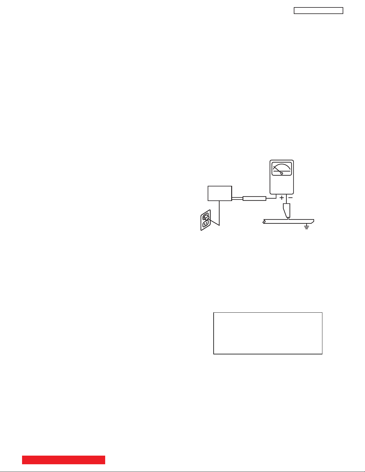
Leakage Current Hot Check
Plug the AC line cord directly into a 120V AC outlet. (Do not use an
isolation transformer during this test.) Use a leakage current
tester or a metering system that complies with the American
National Standards Institute (ANSI) C101.0 Leakage Current
for Appliances. In the case of the LCD, set the AC cable first
in the plugged position and then in the unplugged position,
measure from across Line 1 and Line 2 of the three plug
prongs, do not connect with the third prong, which is physical
ground, to all exposed metal parts of the instrument
(antennas, handle bracket, metal cabinet, screw heads,
metallic overlays, control shafts, etc.), especially any exposed
metal parts that offer an electrical return path to the chassis.
Any current measured must not exceed 0.5 MIU. Reverse the
instrument power cord plug in the outlet and repeat test.
3. When service is required, observe the original lead dress.
4. Always use manufacturer’s replacement components. Critical
components as indicated on the circuit diagram should not be
replaced by another manufacturer’s. Furthermore, where a
short circuit has occurred, replace those components that
indicate evidence of over heating.
5. Before returning a serviced receiver to the customer, the
service technician must thoroughly test the unit to be certain
that it is completely safe to operate without danger of electrical
shock, and be sure that no protective device built into the
receiver by the manufacturer has become defective, or
inadvertently defeated during servicing.
Therefore, the following checks should be performed for the
continued protection of the customer and service technician.
Leakage Current Cold Check
With the AC plug removed from the 120V AC 60Hz source,
place a jumper across Line 1 and Line 2 of the three plug
prongs, do not connect with the third prong, which is physical
ground.
Using an insulation tester (DC500V), connect one of its leads
to the AC plug jumper and touch with the other lead each
exposed metal part (antennas, screwheads, metal overlays,
control shafts, etc.), particularly any exposed metal part
having a return path to the chassis should have a resistor
reading over 4MΩ. Any resistance value below this range
indicates an abnormality which requires corrective action. An
exposed metal part not having a return path to the chassis will
indicate an open circuit.
AC LEAKAGE TEST
(READING
SHOULD NOT
BE ABOVE 0.5MIU)
EARTH
GROUND
DEVICE
UNDER
TEST
TEST ALL
EXPOSED
METAL SURFACES
3-WIRE CORD
ALSO TEST WITH PLUG
REVERSED
(USING AC ADAPTER
PLUS AS REQUIRED)
LEAKAGE
CURRENT
TESTER
ANY MEASUREMENTS NOT WITHIN THE LIMITS OUTLINED
ABOVE ARE INDICATIVE OF A POTENTIAL SHOCK HAZARD
AND MUST BE CORRECTED BEFORE RETURNING THE
RECEIVER TO THE CUSTOMER.
NOTE:
Do not work before the LCD TV set is
unplugged from the power line.
This set does not have a Main Power
Switch.
TABLE OF CONTENTS
2
Page 4

PRODUCT SAFETY NOTICE
Many electrical and mechanical parts in HITACHI television
receivers have special safety-related characteristics. These are
often not evident from visual inspection nor can the protection
afforded by them necessarily be obtained by using replacement
components rated for higher voltage, wattage, etc. Replacement
parts which have these special safety characteristics are
identified in this Service Manual.
Electrical components having such features are identified with a
!
1 mark in the schematics and parts list in this Service Manual.
The use of a substitute replacement component which does not
have the same safety characteristics as the HITACHIrecommended replacement component, shown in the parts list in
this Service Manual, may create shock, fire, X-radiation, or other
hazards.
Product safety is continuously under review and new instructions
are issued from time to time. For the latest information, always
consult the current HITACHI Service Manual. A subscription to,
or additional copies of HITACHI Service Manuals may be
obtained at a nominal charge from HITACHI Sales Corporation.
DW3G
SAFETY NOTICE
USE ISOLATION TRANSFORMER
WHEN SERVICING
POWER SOURCE
This LCD television is designed to operate on 120 Volts/60Hz,,
AC house current. Insert the power cord into a 120 Volts/60Hz
outlet.
NEVER CONNECT THE LCD TV TO OTHER THAN THE
SPECIFIED VOLTAGE OR TO DIRECT CURRENT AND TO
50HZ. TO PREVENT ELECTRIC SHOCK,DO NOT USE THE LCD
TELEVISION’S (POLARIZED) PLUG WITH AN EXTENSION
CORD, RECEPTACLE, OR THE OUTLETS UNLESS THE
BLADES AND GROUND TERMINAL CAN BE FULLY INSERTED
TO PREVENT BLADE EXPOSURE.
L42S601 and L42V651 - LCD TV
1. Follow the general caution recommendations from “Safety
precautions” section.
2. If necessary to replace Panel module, this work must be
started after the panel module and the AC/DC Power supply
becomes sufficiently cool.
3. Special care must be taken with the display area to avoid
damaging its surface.
4. The Panel Module shall not be touched with bare hands to
protect its surface from stains.
5. It is recommended to use clean soft gloves during the
replacing work of the Panel module in order to protect, not
only the display area of the panel module but also the
serviceman.
6. Signal, power supply P.W.B.’s and LCD driving circuits
P.W.B.’s are assembled on the rear side of the LCD module,
take special care with this fragile circuitry; particularly, Flexible
Printed Circuits bonded to surrounding edges of the panel.
They are not strong enough to withstand harsh outer
mechanical forces. Avoid touching the flexible printed circuits
by not only your hands, but also tools, chassis, or any other
object. Extreme bending of the connectors must be avoided
too. In case the flexible printed circuits are damaged, the
corresponding addressed portions of the screen will not be lit
and exchange of the panel will be required.
TABLE OF CONTENTS
3
Page 5

SERVICING PRECAUTIONS
CAUTION: Before servicing instruments covered by this
service data and its supplements and addenda, read and
follow the “Important Safety Instructions” on page 3 of this
publication.
NOTE: If unforeseen circumstances create conflict between
the following servicing precautions and any of the safety
precautions on page 3 of this publication, always follow the
safety precautions. Remember: Safety First.
DW3G
Electrostatically Sensitive (ES) Devices
Some semiconductor (solid state) devices can be damaged
easily by static electricity. Such components commonly are
called Electrostatically Sensitive (ES) Devices. Examples of
typical ES devices are integrated circuits and some fieldeffect transistors and semiconductor “chip” components. The
following techniques should be used to help reduce the
incidence of component damage caused by static electricity.
General Servicing Guidelines
1. Always unplug the instrument AC power cord from the AC
power source before:
a. Removing or reinstalling any component, circuit
board, module, or any other instrument assembly.
b. Disconnecting or reconnecting any instrument
electrical plug or other electrical connection.
c. Connecting a test substitute in parallel with an
electrolytic capacitor in the instrument.
CAUTION: A wrong part substitution or incorrect
polarity installation of electrolytic
capacitors may result in an explosion
hazard.
2. Do not spray chemicals on or near this instrument or any
of its assemblies.
3. Unless specified otherwise in these service data, clean
electrical contacts by applying the following mixture to the
contacts with a pipe cleaner, cotton-tipped stick or
comparable nonabrasive applicator: 10% (by volume)
Acetone and 90% (by volume) isopropyl alcohol (90%99% strength).
CAUTION: This is a flammable mixture. Unless
specified otherwise in these service data,
lubrication of contacts is not required.
4. Do not defeat any plug/socket of voltage interlocks with
which instruments covered by this service data might be
equipped.
5. Do not apply AC power to this instrument and/or any of its
electrical assemblies unless all solid-state device heatsinks are correctly installed.
6. Always connect the test instrument ground lead to the
appropriate instrument chassis ground before connecting
the test instrument positive lead. Always remove the test
instrument ground lead last.
7. Use with this instrument only the test fixtures specified in
this service data.
CAUTION: Do not connect the test fixture ground strap
to any heatsink in this instrument.
1. Immediately before handling any semiconductor
component or semiconductor-equipped assembly, drain
off any electrostatic charge on your body by touching a
known earth ground. Alternatively, obtain and wear a
commercially available discharging wrist strap device,
which should be removed for potential shock reasons
prior to applying power to the unit under test.
2. After removing an electrical assembly equipped with ES
devices, place the assembly on a conductive surface
such as aluminum foil, to prevent electrostatic charge
buildup or exposure of the assembly.
3. Use only a grounded-tip soldering iron to solder or
desolder ES devices.
4. Use only an anti-static type solder removal device. Some
solder removal devices not classified as “anti-static” can
generate electrical charges sufficient to damage ES
device.
5. Do not use freon-propelled chemicals. These can
generate electrical charges sufficient to damage ES
devices.
6. Do not remove a replacement ES device from its
protective package until immediately before you are
ready to install it. (Most replacement ES devices are
packaged with leads electrically shorted together by
conductive foam, aluminum foil or comparable conductive
material.)
7. Immediately before removing the protective material from
the leads of a replacement ES device, touch the
protective material to the chassis or circuit assembly into
which the device will be installed.
CAUTION: Be sure no power is applied to the chassis or
circuit, and observe all other safety
precautions.
8. Minimize bodily motions when handling unpackaged
replacement ES devices. (Otherwise harmless motion
such as the brushing together of your clothes fabric or the
lifting of your foot from a carpeted floor can generate
static electricity sufficient to damage an ES device.)
TABLE OF CONTENTS
4
Page 6
DW3G
General Soldering Guidelines
1. Use a grounded-tip, low-wattage soldering iron and
appropriate tip size and shape that will maintain tip
temperature within the range 500°F to 600°F.
2. Use an appropriate lead free solder (see page 8). Lead
solder can be used, but there is a possibility of failure due
to insufficient strength of the solder.
3. Keep the soldering iron tip clean and well-tinned.
4. Thoroughly clean the surfaces to be soldered. Use a
small wire-bristle (0.5 inch or 1.25 cm) brush with a metal
handle. Do not use freon-propelled spray-on cleaners.
5. Use the following desoldering technique.
a. Allow the soldering iron tip to reach normal
temperature (500°F to 600°F).
b. Heat the component lead until the solder melts.
Quickly draw away the melted solder with an antistatic, suction-type solder removal device or with
solder braid.
CAUTION: Work quickly to avoid overheating the
circuit board printed foil.
6. Use the following soldering technique.
a. Allow the soldering iron tip to reach normal
temperature (500°F to 600°F).
b. First, hold the soldering iron tip and solder strand
against the component lead until the solder melts.
c. Quickly move the soldering iron tip to the junction of
the component lead and the printed circuit foil, and
hold it there only until the solder flows onto and
around both the component lead and the foil.
CAUTION: Work quickly to avoid overheating the
circuit board printed foil or components.
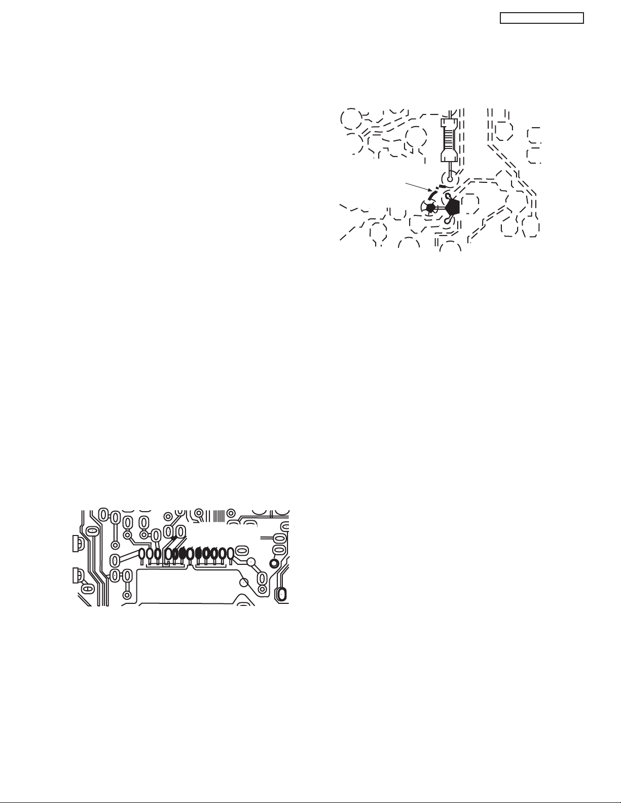
Removal
1. Desolder and straighten each IC lead in one operation by
gently prying up on the lead with the soldering iron tip as
the solder melts.
2. Draw away the melted solder with an anti-static suctiontype solder removal device (or with solder braid) before
removing the IC.
Replacement
1. Carefully insert the replacement IC in the circuit board.
2. Carefully bend each IC lead against the circuit foil pad
and solder it.
3. Clean the soldered areas with a small wire-bristle brush.
(It is not necessary to reapply acrylic coating to areas.)
“Small-signal” Discrete Transistor Removal/Replacement
1. Remove the defective transistor by clipping its leads as
close as possible to the component body.
2. Bend into a “U” shape the end of each of the three leads
remaining on the circuit board.
3. Bend into a “U” shape the replacement transistor leads.
4. Connect the replacement transistor leads to the
corresponding leads extending from the circuit board and
crimp the “U” with long nose pliers to insure metal to
metal contact, then solder each connection.
Power Output Transistor Devices Removal/Replacements
1. Heat and remove all solder from around the transistor
leads.
2. Remove the heatsink mounting screw (if so equipped).
3. Carefully remove the transistor from the circuit board.
d. Closely inspect the solder area and remove any
excess or splashed solder with a small wire-bristle
brush.
Use Soldering Iron to Pry Leads
IC Removal/Replacement
Some Hitachi unitized chassis circuit boards have slotted
holes (oblong) through which the IC leads are inserted and
then bent flat against the circuit foil. When holes are the
slotted type, the following technique should be used to
remove and replace the IC. When working with boards using
the familiar round hole, use the standard technique as
outlined in paragraphs 5 and 6 above.
4. Insert new transistor in circuit board.
5. Solder each transistor lead, and clip off excess lead.
6. Replace heatsink.
Diode Removal/Replacement
1. Remove defective diode by clipping its leads as close as
possible to diode body.
2. Bend the two remaining leads perpendicularly to the
circuit board.
3. Observing diode polarity, wrap each lead of the new
diode around the corresponding lead on the circuit board.
4. Securely crimp each connection and solder it.
5. Inspect (on the circuit board copper side) the solder joints
of the two “original leads”. If they are not shiny, reheat
them and, if necessary, apply additional solder.
5
Page 7
DW3G
Fuses and Conventional Resistor Removal/Replacement
1. Clip each fuse or resistor lead at top of circuit board
hollow stake.
2. Securely crimp leads of replacement component around
stake 1/8 inch from top.
3. Solder the connections.
CAUTION: Maintain original spacing between the
replaced component and adjacent
components and the circuit board, to
prevent excessive component
temperatures.
Circuit Board Foil Repair
Excessive heat applied to the copper foil of any printed
circuit board will weaken the adhesive that bonds the foil to
the circuit board, causing the foil to separate from, or “liftoff,” the board. The following guidelines and procedures
should be followed whenever this condition is encountered.
In Critical Copper Pattern Areas
High component/copper pattern density and/or special
voltage/current characteristics make the spacing and
integrity of copper pattern in some circuit board areas more
critical than in others. The circuit foil in these areas is
designated as Critical Copper Pattern. Because Critical
Copper Pattern requires special soldering techniques to
ensure the maintenance of reliability and safety standards,
contact your Hitachi personnel.
At Other Connections
Use the following technique to repair defective copper
pattern at connections other than IC Pins. This technique
involves the installation of a jumper wire on the component
side of the circuit board.
DEFECTIVE
COPPER
REMOVED
Insulated Jumper Wire
1. Remove the defective copper pattern with a sharp knife.
Remove at least 1/4 inch of copper, to ensure hazardous
condition will not exist if the jumper wire opens.
2. Trace along the copper pattern from both wire sides of
the pattern break and locate the nearest component
directly connected to the affected copper pattern.
At IC Connections
To repair defective copper pattern at IC connections, use the
following procedure to install a jumper wire on the copper
pattern side of the circuit board. (Use this technique only on
IC connections.)
1. Carefully remove the damaged copper pattern with a
sharp knife. (Remove only as much copper as absolutely
necessary.)
2. Carefully scratch away the solder resist and acrylic
coating (if used) from the end of the remaining copper
pattern.
BARE JUMPER
WIRE
CRIMP AND
SOLDER
Install Jumper Wire and Solder
3. Bend a small “U” in one end of a small-gauge jumper wire
and carefully crimp it around the IC pin. Solder the IC
connection.
3. Connect insulated 20-gauge jumper wire from the
nearest component on one side of the pattern break to
the lead of the nearest component on the other side.
Carefully crimp and solder the connections.
CAUTION: Be sure the insulated jumper wire is
dressed so that it does not touch
components or sharp edges.
4. Route the jumper wire along the path of the cut-away
copper pattern and let it overlap the previously scraped
end of the good copper pattern. Solder the overlapped
area, and clip off any excess jumper wire.
6
Page 8
DW3G
NOTE: These components are affixed with glue. Be careful not to break or damage any foil under the
component or at the pins of the ICs when removing. Usually applying heat to the component for a short
time while twisting with tweezers will break the component loose.
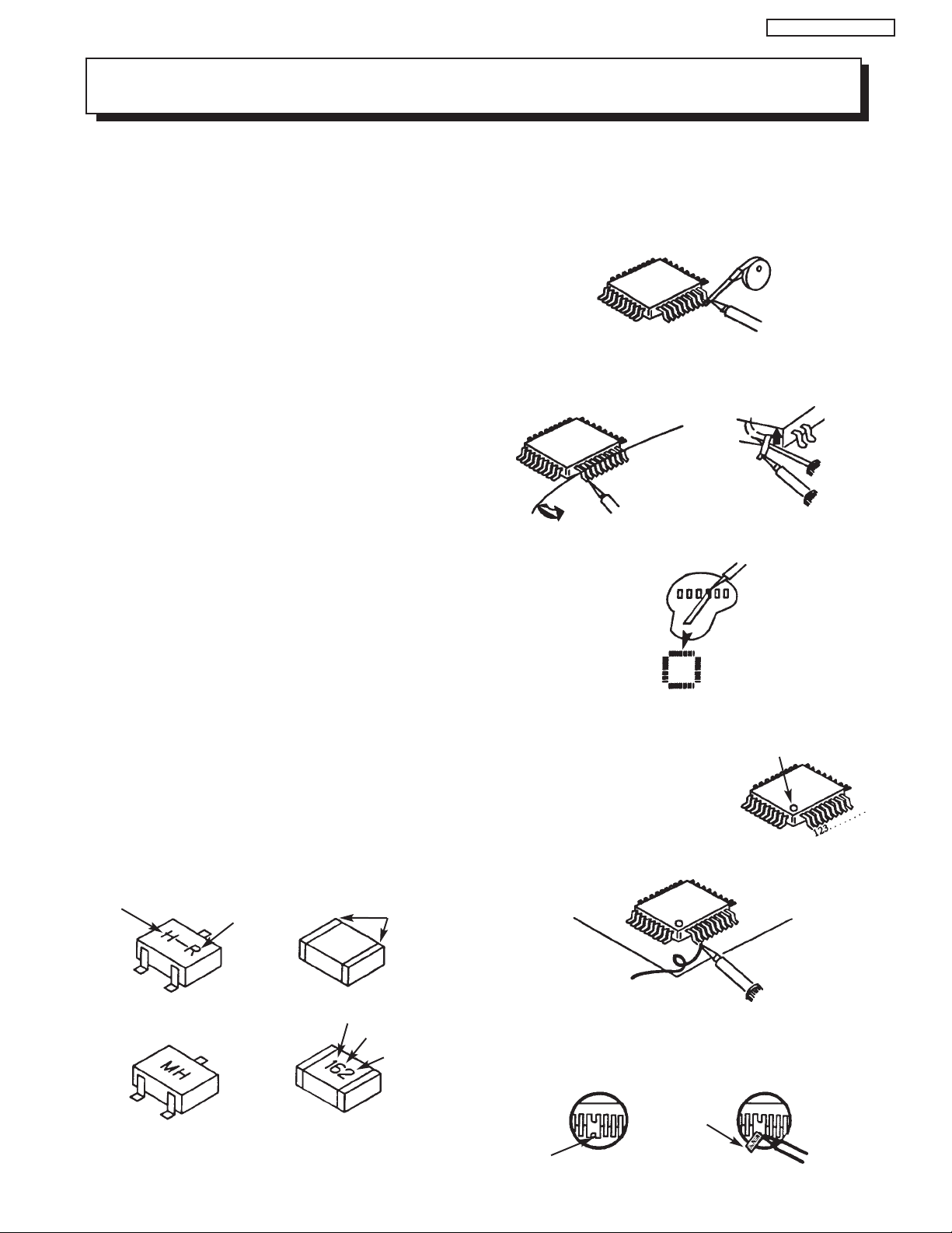
Leadless Chip Components
(surface mount)
Chip components must be replaced with identical
chips due to critical foil track spacing. There are no
holes in the board to mount standard transistors or
diodes. Some chip capacitor or resistor board solder
pads may have holes through the board, however the
hole diameter limits standard resistor replacement to
1/8 watt. Standard capacitors may also be limited for
the same reason. It is recommended that identical
chip components be used. .
Chip resistors have a three digit numerical resistance
code -1st and 2nd significant digits and a multiplier.
Example: 162 = 1600 or 1.6KΩ resistor, 0 = 0Ω
(jumper).
Chip capacitors generally do not have the value
indicated on the capacitor. The color of the component
indicates the general range of the capacitance.
Chip transistors are identified by a two letter code. The
first letter indicates the type and the second letter, the
grade of transistor.
Chip diodes have a two letter identification code as
per the code chart and are a dual diode pack with
either
common anode or common cathode. Check the parts
list for correct diode number.
Component Removal
1. Use solder wick to remove solder from component
end caps or terminals.
2. Without pulling up, carefully twist the component
with tweezers to break the adhesive.
3. Do not reuse removed leadless or chip
components since they are subject to stress
fracture during removal .
Chip Component Installation
1. Put a small amount of solder on the board
soldering pads.
2. Hold the chip component against the soldering
pads with tweezers or with a miniature alligator
clip and apply heat to the pad area with a 30 watt
iron until solder flows. Do not apply heat for more
than 3 seconds
TYPE
Chip Components
C
GRADE
SOLDER
CAPS
How to Replace Flat-lC
—Required Tools—
• Soldering iron • iron wire or small awl
• De-solder braids • Magnifier
1. Remove the solder from all of the pins of a Flat-lC
by using a de-solder braid.
De-Solder
Braid
Soldering
Iron
2. Put the iron wire under the pins of the Flat-lC and
pull it in the direction indicated while heating the
pins using a soldering iron. A small awl can be
used instead of the iron wire.
Pull
Soldering
Iron
3. Remove the solder from all of the pads of the
Flat-lC by using
a de-solder braid.
4. Position the new Flat-lC in place (apply the pins of
the Flat-lC to the soldering pads where the pins
need to be soldered). Properly
determine the positions of the
soldering pads and pins by
correctly aligning the polarity
symbol.
5. Solder all pins to the soldering pads using a fine
tipped soldering iron.
Iron
Wire
Awl
Soldering
Iron
Soldering
Iron
De-Solder
Braid
Flat-IC
Polarity Symbol
B
ANODES
E
COMMON CATHODE
MH DIODE
TRANSISTOR
SOLDER CAPS
1ST DIGIT
RESISTOR
CAPACITOR
2ND DIGIT
MULTIPLIER
= 1600 = 1.6K
Solder
Soldering
Iron
6. Check with a magnifier for solder bridge between
the pins or for dry joint between pins and soldering
pads. To remove a solder bridge, use a de-solder
braid as shown in the figure below.
De-Solder
Braid
Bridge
Solder
7
Soldering
Iron
Page 9
Information for service about lead-free solder introduction
Hitachi introduced lead-free solder to conserve the "Earth Environment".
Please refer to the following before servicing.
(1) Characteristic of lead-free solder
Melting point of lead free solder is 40-50
(2) Solder for service
Following composition is recommended.
" Sn - 3.0Ag - 0.5Cu " , or " Sn - 0.7 Cu "
Lead solder can be used, but there is a possibility of failure due to insufficient strength of the solder.
Caution when using solder containing lead.
Please remove previous solder as much as possible from the soldering point.
When soldering, please perfectly melt the lead-free solder to mix well with the previous solder.
(3) Soldering iron for lead-free solder.
Melting point of lead-free solder is higher than solder containing lead.
Use of a soldering tool "with temperature control" and "with much thermal capacitance" is recommended.
(Recommended temperature control : 320
o
C higher than solder containing lead.
o
C - 450oC)
DW3G
Recommended temperature
PWB with chip parts
PWB without chip parts
Chassis, metal, shield etc.
320oC +/- 30oC
380oC +/- 30oC
420oC +/- 30oC
(4) Identification of lead-free PWB
2004 models >> lead-free solder is introduced
2006 models >> lead-free solder apply
On lead-free PWB, "F" is added at the beginning of stamp on PWB. (e.g. F DW3-TERMINAL)
8
Page 10

AGENCY REGULATORY
INFORMATION
Federal Communications Commission Notice
This equipment has been tested and found to comply with the limits for a Class B digital device, pursuant to Part
15 of the FCC Rules. These limits are designed to provide reasonable protection against harmful interference in
a residential installation. This equipment generates, uses and can radiate radio frequency energy and if not
installed and used in accordance with the instructions, may cause harmful interference to radio
communications. However, there is no guarantee that interference will not occur in a particular installation. If this
equipment does cause harmful interference to radio or television reception, which can be determined by turning
the equipment off and on, the user is encouraged to try to correct the interference by one or more of the
following measures:
• Reorient or relocate the receiving antenna.
• Increase the separation between the equipment and the receiver.
• Connect the equipment into an outlet on a circuit different from that to which the receiver is connected.
• Consult the dealer or an experienced radio/television technician for help.
FCC Information
This device complies with part15 of the FCC Rules.Operation is subject to the following two conditions :
(1) This decide may not cause harmful interference and (2) This decide must accept any interference
received, including interference that may cause undesired operation.
DW3G
Modifications
The FCC requires the user to be notified that any changes or modifications made to this device that are not
expressly approved by Hitachi America ,Ltd. Home Electronics Division may void the user’s authority to
operate the equipment.
Cables
Connections to this device must be made with shielded cables with metallic RFI/EMI connector hoods to
maintain compliance with FCC Rules and Regulations.
Any cables that are supplied with the system must be replaced with identical cables in order to assure
compliance with FCC rules. Order Hitachi spares as replacement cables.
Note
This LCD Televisionreceiver will display television closed captioning,(or),in accordance with
paragraph 15.119 of the FCC rules.
INDUSTRY CANADA AGENCY REGULATORY INFORMATION
Cable Compatible Television Apparatus- Tèlèvision câblocompatible, Canada.
This Class B digital apparatus meets all requirements of the Canadian Interference-Causing Equipment Regulations.
This Class B digital apparatus complies with Canadian ICES-003.
Cet appareil numérique de la classe B est conforme à la norme NMB-003 du Canada.
TABLE OF CONTENTS
9
Page 11
ACKNOWLEDGMENTS
HDMI, the HDMI logo and High-Definition Multimedia
Interface are trademarks or registered trademarks of HDMI Licensing
LLC.
AND TRADEMARKS
*Manufactured under license from Dolby Laboratories. “Dolby” and the double-D symbol are
trademarks of Dolby Laboratories.
㪚㪦㪧㪰㪩㪠㪞㪟㪫㩷㪺㩷㪈㪐㪐㪐㪄㪉㪇㪇㪍㩷㪤㪦㪥㪫㪘㪭㪠㪪㪫㪘㩷㪪㪦㪝㪫㪮㪘㪩㪜㪃㩷㪠㪥㪚㪅㩷㪘㪣㪣㩷㪩㪠㪞㪟㪫㪪㩷㪩㪜㪪㪜㪩㪭㪜㪛㪅
DW3G
TABLE OF CONTENTS
10
Page 12
DW3G
INTRODUCTION
This HITACHI Service Manual is intended for the qualified service personnel and it contains the necessary information for
troubleshooting the LCD television set in case of malfunction.
This service manual includes the information for the next models and chassis.
MODEL CHASSIS
L42S601 DW3G
L42V651 DW3G
DIMENSIONS:
Height: 743 mm(with table top stand).
Width: 1041.7 mm
Depth: 366 mm (with table top stand).
POWER RATINGS:
P
ST(W)
With POD.
less than 14W
Chassis
No.
Model Name
Indicated Value
Max Rating
(W) (A)
Average
Rating (W)
Without POD.
less than 1W
1 L42S601 215 1.85 215 0.6 - DW3G
2 L42V651 215 1.85 215 0.6 - DW3G
CIRCUIT PROTECTION
CAUTION: Below is an EXAMPLE only. See Replacement Parts List for details. The following symbol near the fuse
Example:
“RISK OF FIRE - REPLACE FUSE AS MARKED”
indicates fast operation fuse (to be replaced). Fuse ratings appear within the symbol.
F
8 A 125V
The rating of fuse F1 is 8 A- 125V.
Replace with the same type fuse for continued protection
against fire.
8 A
125V
TABLE OF CONTENTS
11
Page 13
DW3G
SPECIFICATIONS
APPEARANCE
Model name Series Name Cabinet Design
L42S601 UltraVision
L42V651 UltraVision
Gloss Black/Frame, High Gloss Black/Bezel, High Gloss Hidden/SP
Gloss Black/Frame, High Gloss Black/Bezel,High Gloss Hidden/SP
SYSTEM
Channel coverage band Reception system
No. Model name VHF(ch) UHF(ch) CATV(ch) NTSC ATSC 64QAM/
(8VSB) 256QAM
1 L42S601 2~13 14~69 A-5~A-1, A
I,J W,W+1 W+94 X X X
~~ ~
2 L42V651 X X X
STRUCTURAL DIMENSIONS
No. Model name WIDTH HEIGHT DEPTH WEIGHT
[mm] [mm] [mm] [kg] Note
1 L42S601 1041.7 743* 366* 27.8
2 L42V651 1041.7 743* 366* 27.8
*With table top
stand.
*With table top
stand
EXTERNAL TERMINALS AND JACKS
Model Rear
name A/V S COMP. HDMI M A Subwoofer ANT OPT DV IN POD
IN IN IN OUT OUT OUT IN OUT IEEE 1394 CARD
L42S601 3 1 2 2 1 1 - 1 1 - -
L42V651 3 1 2 2 1 1 - 1 1 - -
Model Front Rear
name A/V S COMP. HDMI Photo Upgrade DV IR OUT IR OUT SWIVEL RS232C
IN IN IN (SD) IN /G-LINK OUT
L42S601 1 - - 1 - 1 -(1:Service) - 1 1
L42V651 1 - - 1 1 1 -(1:Service) - 1 1
MAIN FEATURES
No. Feature L42S601 L42V651
1 Panel LPL LPL
2 Resolution
3
4 Seine2 X X
5 FRC (FC8)
6 One NTSC/ATSC Tuner X X
7 POD (Point Of Deployment)
8 PinP (Digital/External Analog SPLIT)
9 3 Picture Mode X X
10 Color Temperature Mode 4 4
11 Color Decoding Adjustment
12 Color Management Adjustment
13 7 Mode Aspect Ratio Interchangeable X X
Front Filter with ARF
(Transparency)
1920x
1080p
- -
- -
- -
- X
- -
- -
1920x
1080p
No. Feature L42S601 L42V651
14 EPG (G-GUIDE) Function
15 SD-card Photo Viewer - X
16 Audio Output 10W x2 10W x2
17 Swivel Power Power
18 AV NET, AV NET Learning
19 IR Pass Through
20 OSD Design B C
21 Energy Star
- -
- -
- -
- -
TABLE OF CONTENTS
12
Page 14
POWER CONSUMPTION
MODEL INDICATED VALUE PST [W] CHASSIS
NAME Max. Rating Max. Rating (Average Rating) Without POD With POD
L42S601 215W 1.85A 215W 0.6W - DW3G
L42V651 215W 1.85A 215W 0.6W - DW3G
SAFETY KEY COMPONENTS
No. Model Symbol No. P# (Rating) Standard
1
2
3
L47S601/V651, L42S601/V651
L47S601/V651, L42S601/V651
L47S601/V651, L42S601/V651
NOTE: The FUSE is in the power supply unit.
(note)
:
(
note)
:
(
note)
:
F1 FN00476
F201
F101
8A/125V UL/CSA
()
4A/250V UL/CSA
()
1A/250V UL/CSA
()
DW3G
TABLE OF CONTENTS
13
Page 15
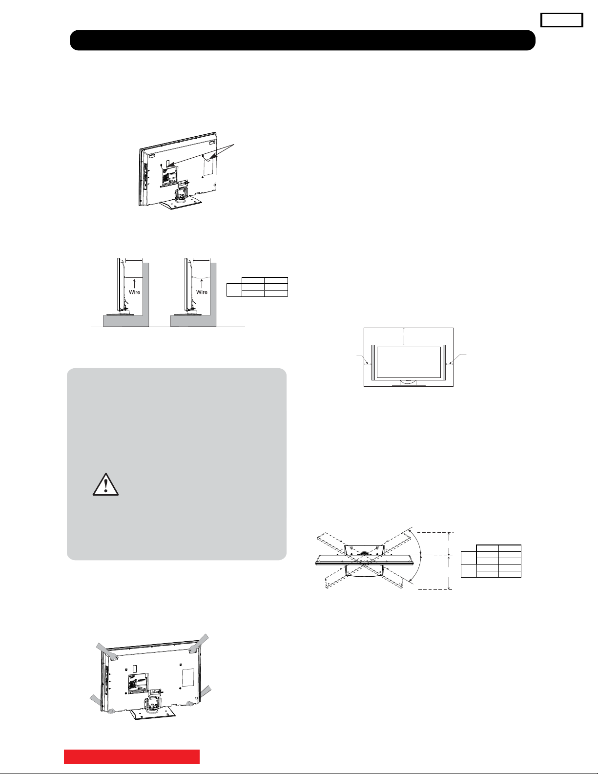
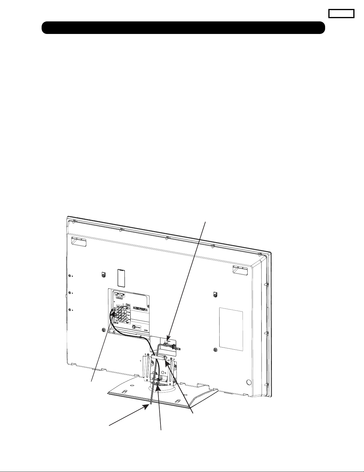
How To Set Up Your New Hitachi LCD Television
To take measures to prevent the LCD Flat Panel Television from tipping over and prevent possible injury
it is important to mount the unit in a stable and flat surface.
DW3G
Securing to a Wall
1. Using metallic wire (two places) fasten the set to
the clamping screw on the rear of the LCD Flat
Panel TV as shown below.
Wire
2. Keep the LCD television 4 inches away from the
wall except when mounted using the wall mount
bracket.
3.Secure the television to the wall as shown.
A
(a) Power Swivel
NOT USED
B
(b) Power Swivel
USED
A B
12
in.
5 in.
42”
47”
1
2.5 cm
30 cm
* Please adjust the wire length to avoid
touching the wall when turning the TV.
NOTES: 1. Do not block the ventilation holes of the
LCD Television. Blocking the ventilation
holes might cause fire or defect.
2. In case of an abnormal symptom, unplug
the AC cord.
3. If you purchased the wall mount bracket
option, please ask for professional installer.
Do not install by yourself.
4. Install the unit at a proper area where it does
not expose anyone to any danger of hitting
themselves (for example their hands, head
or face, etc.) against the edge of the unit and
cause personal injury.
5. If the Power Swivel feature will not be
used, the LCD television should be
secured to the wall as shown in
fig. (a).
6. If the Power Swivel feature will be used,
the LCD television should be secured
to the wall as shown in
fig. (b).
Caution when moving the main unit
As this product is heavy, whenever it is moved, two
people are required to transport it safely. Whenever the
unit is moved it should be lifted forward using the top
and base on both sides of the Television for stability.
When moving the Television, lift the handles , then
support the bottom frame as shown below.
ANTENNA
Unless your LCD Television is connected to a cable
TV system or to a centralized antenna system, a good
outdoor color TV antenna is recommended for best
performance. However, if you are located in an
exceptionally good signal area that is free from
interference and multiple image ghosts, an indoor
antenna may be sufficient.
LOCATION
Select an area where sunlight or bright indoor
illumination will not fall directly on the picture screen.
Also, be sure that the location selected allows a free
flow of air to and from the perforated back cover of the
set. In order to prevent an internal temperature
increase, maintain a space of 10 cm (4 inches) from the
sides/back of the Television, and 30 cm (12 inches)
from the top of the television to the ceiling. To avoid
cabinet warping, cabinet color changes, and increased
chance of set failure, do not place the TV where
temperatures can become excessively hot, for
example, in direct sunlight or near a heating appliance,
etc.
30 cm (12 inches)
10 cm (4 inches)
10 cm (4 inches)
CONNECT POWER SWIVEL CABLE
Connect one end of cable to the swivel slot of the
LCD Rear Panel. Connect the other end to swivel
slot of the Table Top Stand. For more detail information,
please refer to next page installation instruction.
TURNINGANGLE
The maximum turning angle is 30° (left and right). Do
not place any objects on the path of the monitor when
using the power swivel feature.
C
30°
30°
D
C D
9.1 in.
4.05 in.
3.1
2
10.2 in.
5.9
2
cm
cm
1
35.7 cm
15.15 in.
38.5 cm
42"
47"
47” & 42 "
TABLE OF CONTENTS
14
14
Page 16
How to set up your new Hitachi LCD Television
AC CORD AND POWER SWIVEL CABLE INSTALLATION INSTRUCTION
The AC cord and power swivel cable provided with your new LCD Flat Panel Television need to be installed correctly
to avoid their disconnection when rotating the TV on its Table top stand.
Located on the back of the TV are 2 plastic clamps to hold the AC cord and power swivel cable. Please follow
the instructions below.
쐃
Pass the AC cord through Clamp #1 and connect
it to the TV. Pull on the clamp to tighten the
AC cord to the TV.
쐇
Connect power swivel cable on one end to the
swivel slot of the
the other end to the swivel slot of the Table
T
op Stand Base.
The AC cord, power swivel cable and the signal
쐋
cables can all be held together with Clamp #2.
LCD Rear Panel. Connect
DW3G
Clamp #1 : Pass the AC cord through this clamp ;
쐃
then pull the clamp to tighten the AC
cord to the TV.
Swivel slot on the
쐇
LCD back panel.
AC CORD
Swivel slot on Table Top
쐇
Stand Base.
Clamp #2: Use this clamp to hold the AC cord, power
쐋
15
swivel connector and the signal cables.
Page 17
How to set up your new HITACHI LCD Television
SETTING FOR WALL MOUNTING
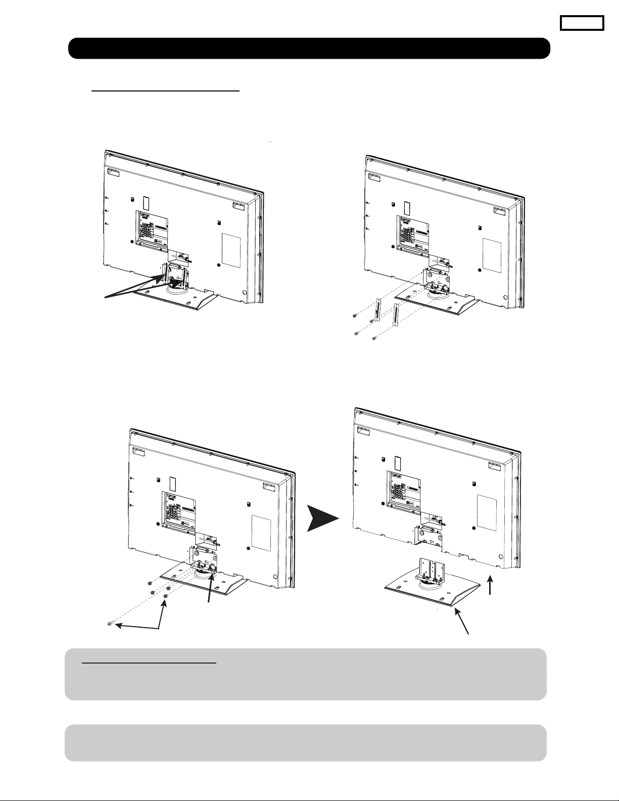
STEP (1) :
Please locate the STAND METAL SUPPORTS on the back of the TV . These metals is use to hold the TV and the Base ;
so it needs to remove 4 screws from the STAND METAL in order to separate the TV from the Base.
2 STAND METAL
SUPPORTS
DW3G
Remove 4 screws
then remove the 2 metal
supports.
STEP (2):
Now please remove the 5 screws of the STAND metal from the TV, now the TV STAND can be separated from the
TV.
STAND METAL
5 SCREWS
TV STAND BASE
For Model L42S601 & L42V651
CAUTION- This LCD Flat Panel for use only with Hitachi WM07S Wall Mount. Use with other
Wall Mount is capable of resulting in instability causing possible injury.
NOTE: Use the specified WALL MOUNT unit for the LCD TV depending on the size of your TV.
Please access our web site at: www.hitachi.us/tv (US) or www.hitachi.ca/tv (CAN) for
recommended accessories for your TV.
16
Page 18
How to set up your new HITACHI LCD Television
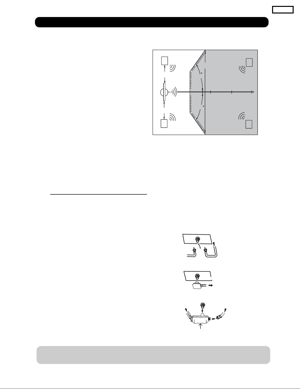
VIEWING
The best picture is seen by sitting directly in front of
the TV and about 10 to 18 feet from the screen.
DW3G
During daylight hours, reflections from outside light
may appear on the screen. If so, drapes or screens
can be used to reduce the reflection or the TV can
be located in a different section of the room.
If the TV’s audio output will be connected to a Hi-Fi
system’s external speakers, the best audio
performance will be obtained by placing the
speakers equidistant from each side of the receiver
cabinet and as close as possible to the height of
the picture screen center. For best stereo
separation, place the external speakers at least
four feet from the side of the TV, place the surround
speakers to the side or behind the viewing area.
Differences in room sizes and acoustical
environments will require some experimentation
with speaker placement for best performance.
ANTENNA CONNECTIONS TO REAR JACK
PANEL
R
4" Minimum
4" Minimum
L
S
80
BEST
HORIZONTAL
5'
10'
VIEWING ANGLE
80
15' 20'
S
VHF (75-Ohm) antenna/CATV (Cable TV)
When using a 75-Ohm coaxial cable system, connect CATV coaxial cable to the AIR/CABLE (75-Ohm) terminal.
Or if you have an antenna, connect the coaxial cable to the same AIR/CABLE terminal.
AIR / CABLE
To CATV cable
VHF (300-Ohm) antenna/UHF antenna
When using a 300-Ohm twin lead from an outdoor
antenna, connect the VHF or UHF antenna leads to
screws of the VHF or UHF adapter. Plug the adapter
To outdoor antenna
or
into the antenna terminal on the TV.
AIR / CABLE
When both VHF and UHF antennas are
connected
Attach an optional antenna cable mixer to the TV
antenna terminal, and connect the cables to the
antenna mixer. Consult your dealer or service store for
the antenna mixer.
To UHF
antenna
AIR / CABLE
Antenna Mixer
To outdoor VHF
or UHF antenna
To outdoor antenna
or CATV system
NOTE: Connecting a 300-Ohm twin lead connector may cause interference. Using a 75-Ohm coaxial
cable is recommended.
17
Page 19
Hook-up Cables and Connectors
Most video/audio connections between components can be made with shielded video and audio cables that have
phono connectors. For best performance, video cables should use 75-Ohm coaxial shielded wire. Cables can be
purchased from most stores that sell audio/video products. Below are illustrations and names of common
connectors. Before purchasing any cables, be sure of the output and input connector types required by the
various components and the length of each cable.
DW3G
300-Ohm Twin Lead
Cable
This outdoor antenna cable must be connected to an
antenna adapter (300-Ohm to 75-Ohm).
Phono or RCA
Cable
Used on all standard video and audio cables which
connect to inputs and outputs located on the
television’s rear jack panel and side control panel.
“F” Type 75-Ohm Coaxial Antenna
For connecting RF signals (antenna or cable TV) to the
antenna jack on the television.
S-Video (Super Video)
Cable
This connector is used on camcorders, VCRs and laserdisc players with an S-Video feature in place of the
standard video cable to produce a high quality picture.
Optical Cable
This cable is used to connect to an audio amplifier with
an Optical Audio In jack. Use this cable for the best
sound quality.
HDMI Cable
This cable is used to connect your external devices
such as Set-Top-Boxes or DVD players equipped with
an HDMI output connection to the TV’s HDMI input.
Stereo Cable (3.8mm plug to 3.5mm plug)
Used on all standard video and audio cable which
connect to inputs and outputs located on the rear jack
panel and side control panel.
Power Swivel Cable (Provided)
This cable is used to connect the swivel stand to the
rear panel of the LCD Television.
AUDIO OUT
3.8mm
STEREO
MINI-PLUG
2
RCA TYPE
PLUGS
18
Page 20
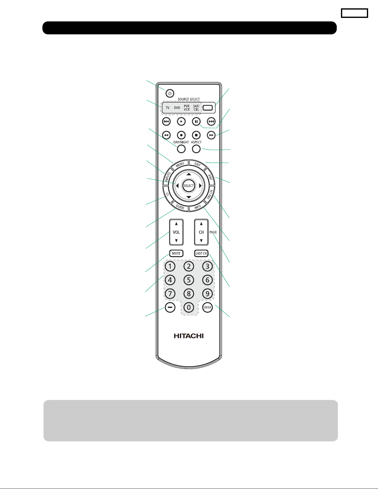
Quick Reference Remote Control Buttons and Functions
In addition to controlling all of the functions on your HITACHI LCD TV, the new remote control is designed to
operate different types of devices, such as, DVD Players, CBL (Cable Boxes), set-top-boxes, satellite receivers,
and VCRs. The remote control must be programmed to control the chosen device.
DW3G
(TV, DVD, SAT/CBL,PVR/VCR)
T
urns the selected device on and o.
Turns on or blinks to show remote control
mode when the SOURCE ACCESS buttons
are pressed.
Toggles picture mode settings
between DAY and NIGHT mode.
(TV,DVD,SAT/CBL,PVR/VCR)
Accesses the OSD menu system.
Accesses the INPUTS menu system.
CURSOR PAD/SELECT BUTTON
(TV, DVD, SAT/CBL,PVR/VCR)
The Cursor Pad is used as a cursor to navigate
through the OSD and INPUT menu systems.
The Select button is used to Select/Activate
highlighted menu items.
Closed Caption (CC) BUTTON
Press to show and change the
Closed Caption mode.
Accesses the program guide of other devices.
Increase up and decrease down to adjust
the audio level of your TV
Reduces the audio level to 50% if pressed
once, and to complete mute if pressed
twice. Press it a third time to restore audio
level.
Used to manually enter the TV channel, and used
for numeric entry when navigating through the
the OSD, INPUTS.
The (-) button is used when the remote is in
Set-Top-Box (STB) mode or when the TV uses a
digital input.
(TV, DVD, SAT/CBL, PVR/VCR)
POWER BUTTON
MODE INDICATOR
DAY/NIGHT BUTTON
MENU BUTTON
INPUTS BUTTON
GUIDE BUTTON
(SAT/CBL, PVR)
VOLUME BUTTONS
MUTE BUTTON (TV)
NUMERIC BUTTONS
.
(-) BUTTON
(TV,STB)
(TV)
(TV)
(TV)
(TV )
SOURCE ACCESS BUTTONS
, DVD, PVR/VCR, SAT/CBL)
(TV
Changes the mode of the Universal Remote
Control to control the device selected.
P
AUSE BUTTON
(TV,PVR/VCR, DVD)
Press to
pause other devices when the remote is
in
DVD, PVR/VCR mode or to show and change the
Frezze mode of the TV(L42V651 Only).
DVD/VCR CONTROL BUTTONS
(DVD, PVR/VCR)
Controls the functions of your VCR
ASPECT BUTTON
(TV)
Changes the aspect ratio of the TV.
EXIT BUTTON
(TV, SAT/CBL, PVR/VCR)
Exits out of the OSD, INPUTS menu
systems if their menu is displayed.
ANT (Antenna) BUTTON
(TV)
Press for change to antenna input.
PIP CONTROL BUTTON in L42V651
(TV)
P ress to s how and change the P icture-in-P icture mo de.
FAVORITE CHANNEL
FAV CH) button (TV)
(
Press to enter/access Favorite Channel (FAV CH) mode.
(Favorite channel is only available for TV mode.)
INFO BUTTON
V, STB, CBL, PVR)
(T
Displays various information on the
screen, such as channel information.
CHANNEL UP & DOWN BUTTONS
(TV, CBL, STB, PVR/VCR)
Changes up or down the channel.
LAST CHANNEL BUTTON
V, SAT/CBL, PVR)
(T
Switches between the current and last channel viewed.
ENTER BUTTON
(TV, VCR, SAT/CBL)
Press to use as SELECT feature.
and DVD.
-L42S601
LEGEND
TV – Television PVR – Video Recorder/Player
CBL – Cable Box DVD – Digital Video Disc Player
SAT –
Satellite
VCR – Videocassete Recorder
NOTES: 1. The TV’s remote control sensor is located on the right bottom portion of the TV screen. To
control TV functions, please point the remote control directly at the remote control sensor for
best results.
VCR precode is included in the PVR mode.
2.
19
Page 21
FRONT VIEW
SIDE PANEL
CONTROLS
Side Panel Controls
햲
햶
햷
햵
햳
햻
햴
DW3G
햲SIDE POWER button
Press this button to turn the LCD Television
ON/OFF. It can also be turned ON/OFF by remote
control. The “MAIN POWER” can only be turn OFF
by unplugging the power cord from the outlet.
After this button is pressed to turn ON the set,
the function of this button will not be available
for a short period of time until the picture appears
on the TV screen.
NOTE:When the TV is unplugged, the clock will
stop and may eventually reset itself.
햳MENU/SELECT button
This button allows you to enter the MENU, making
it possible to set TV features to your preference
without using the remote. This button also serves
as the SELECT button when in MENU mode.
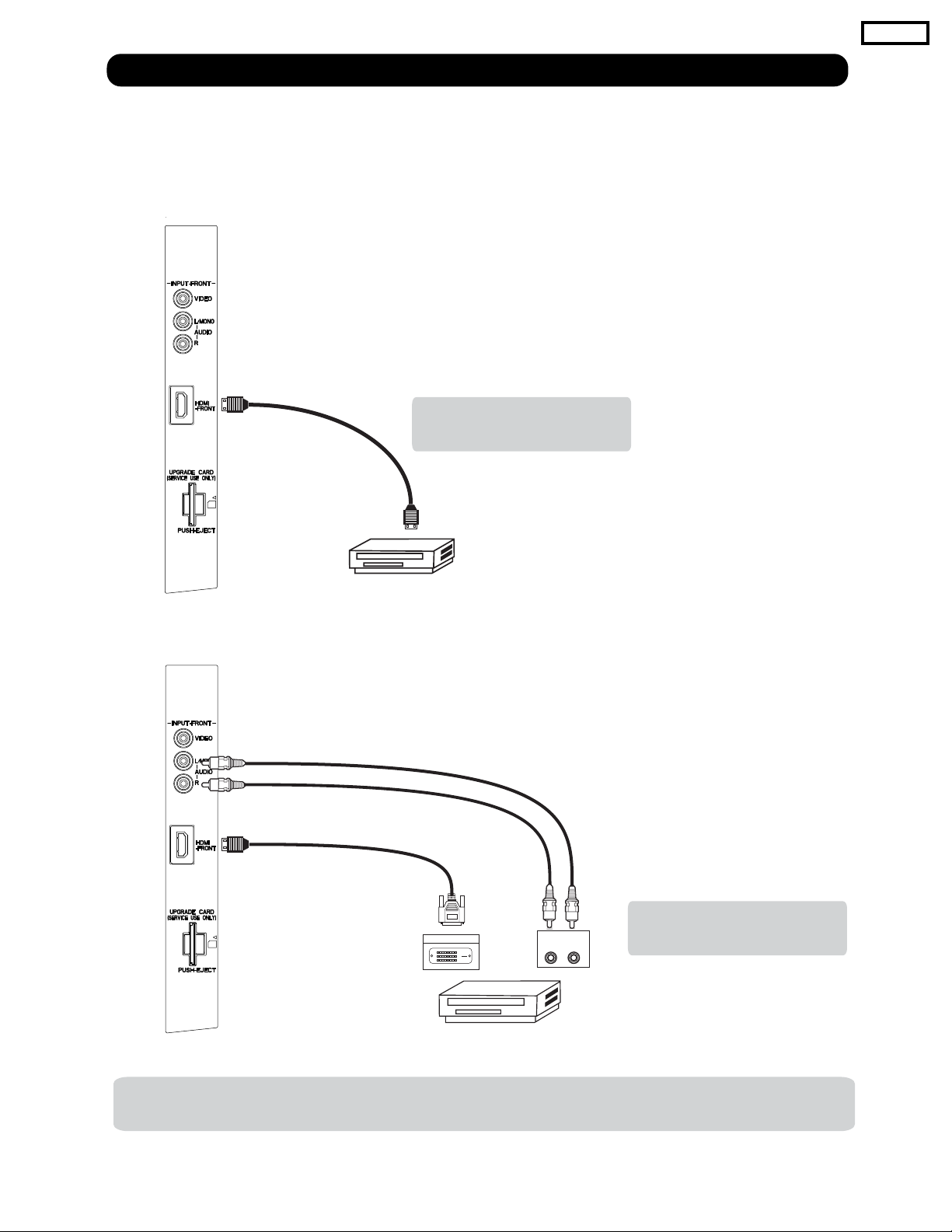
HDMI-FRONT
햴
Use the side HDMI input for external devices such
as Set-Top-Boxes or DVD players equipped with an
HDMI output connection.
햺 햹
햶 CHANNEL selector
Press these buttons until the desired channel
appears in the top right corner of the TV screen.
These buttons also serve as the cursor down ()
and up () buttons when in MENU mode.
햷 VOLUME level
Press these buttons to adjust the sound level. The
volume level will be displayed on the TV screen.
These buttons also serve as the cursor left () and
right () buttons when in MENU mode.
햸
Upgrade Card
This ca
rd slot is for future software upgrades.
Hitachi will notify you if a software upgrade is
required for your TV. In order to receive written
notification, please complete and return your
warranty card.
햸
SD CARD PHOTO INPUT (L42V651 only)
To view digital still pictures, please insert an
card in to the card slot with pictures taken on a
Digital camera, to view them on the TV screen.
햸
SD/MMC
햵INPUT/EXIT button
Press this button to access the INPUT menu.
Press again to exit the MENU mode.
20
Page 22
Side Panel Controls
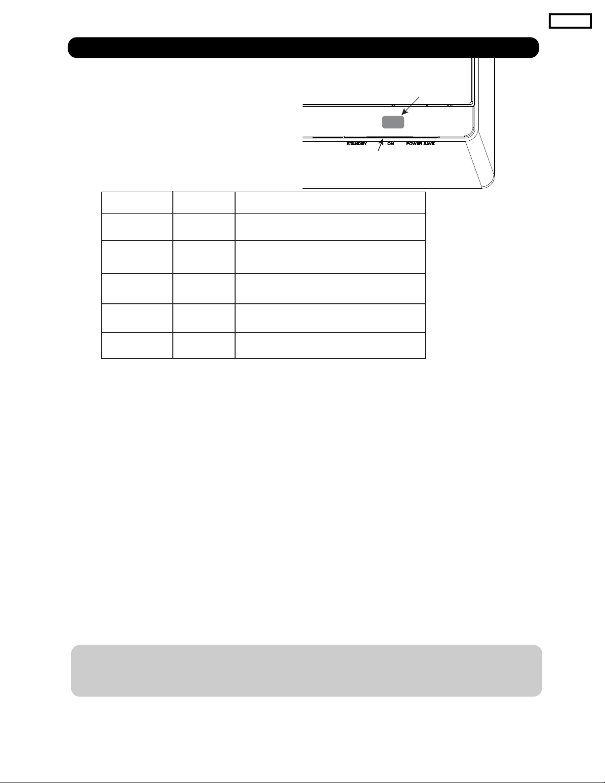
햹
POWER light indicator
To turn the TV ON, press the power button
located on the right side of the TV set.
A red stand-by indicator lamp located on
the lower right corner of the front bezel
is illuminated. The LCD TV is now ready for
remote ON/OFF operation.
Indicating Lamp Power Status Operating
햹
Indicating Lamp
햺
R/C sensor
DW3G
Off
Lights
Red
Lights
TV POWER is ON ; picture is shown.
Blue
Lights
Orange
Blinking
Blue
REMOTE CONTROL sensor
햺
Point your remote at this area when selecting
channels, adjusting volume, etc.
햻
INPUT- FRONT JACKS
INPUT- FRONT provide composite Video jacks for
connecting equipment with this capability,
such as a DVD player or Camcorders.
OFF. When the TV set is unplugged from AC line.
F.
OF
(Stand-by)
On
Off
(Power Saving)
When TV receives the IR signal from R/C.
On
When the TV set is plugged to the AC line.
TV POWER is ON with no signal input
except antenna (no sync. signal).
NOTES: 1. Your HITACHI LCD TV will appear to be turned OFF (lights orange) if there is no video input
when INPUT : 1, 2, 3, Front and HDMI 1, 2 , Front. Check the Power Light to make sure the TV
is turned off or in Stand-by mode (lights red) when not in use.
2.Remote Control can not turn ON/OFF the “MAINPOWER” of the TV.
21
Page 23
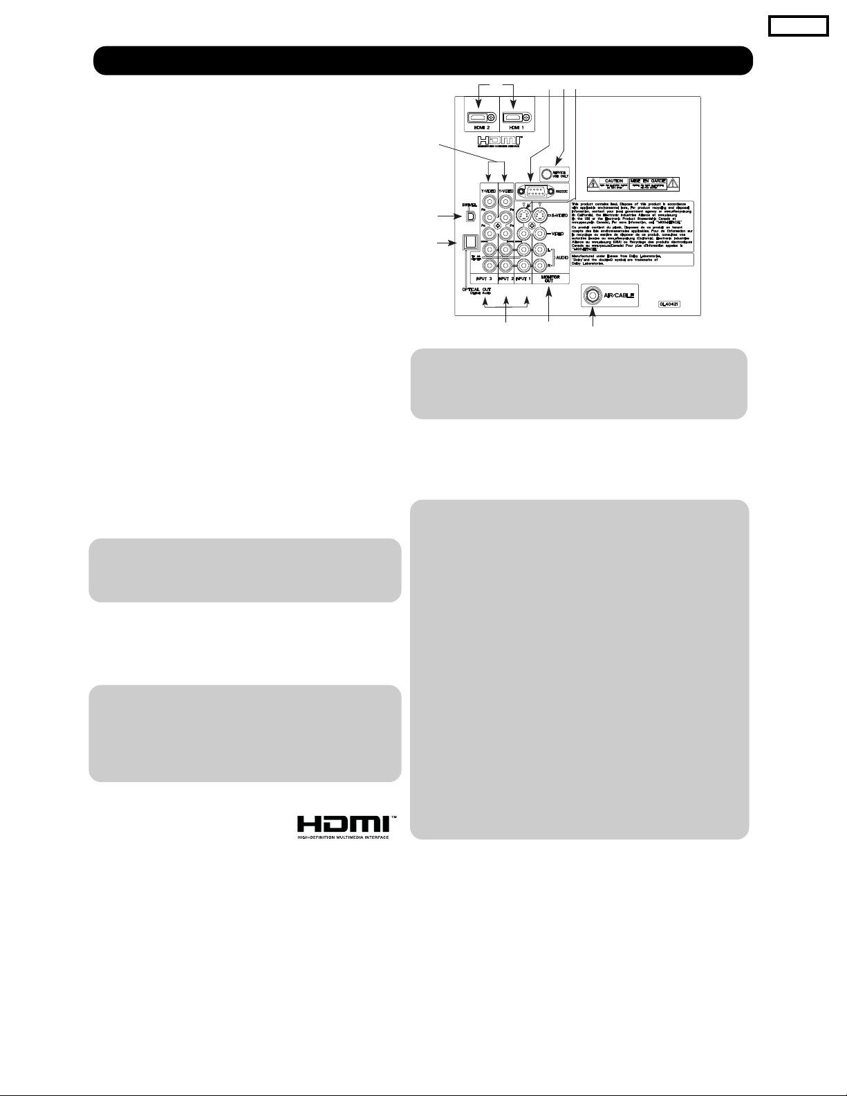
Rear Panel Connections
햲Antenna Input
To switch between Cable and Air input, go to the
Channel Manager option to change the signal
source CABLE or AIR.
Audio/Video Inputs 1, 2 and 3
햳
By using the INPUTS button, the CURSOR PAD (
), and the SELECT button or CURSOR PAD
and
of the remote control, you can select each video
rce. Use the audio and video inputs to connect
sou
external devices, such as VCRs, camcorders,
laserdisc players, DVD players etc. (if you have
mono sound, insert the audio cable into the left
audio jack).
햴
MONITOR OUT &AUDIO OUT
These jacks provide fixed audio and video
signals (CABLE/AIR or INPUTS ) which are
used for recording. Use the S-VIDEO output
for high quality video output. Component signal
to Input 2 and 3, and HDMI inputs will not
have monitor output.
햵 Optical Out (Digital Audio)
This jack provides Digital Audio Output for your
audio device that is Dolby
compatible, such as an audio amplifier
® Digital and PCM
.
NOTE: *Manufactured under license from Dolby
Laboratories. “Dolby” and the double-D
symbol are trademarks of Dolby
Laboratories.
햶 S-VIDEO
Input 1
Input 1 provide S-VIDEO (Super Video)
jacks for connecting equipment with S-VIDEO
output capability
N
1. You may use VIDEO or S-VIDEO inputs to
OTE:
.
connect to INPUT 1 , but only one of
these inputs may be used at a time.
2. S-VIDEO output may be used for
recording, only when the input is of
S-VIDEO type.
햷 HDMI 1, 2 (High Definition Multimedia
Interface)
ABOUT HDMI
– HDMI
is the
next-generation all digital interface for consumer
electronics. HDMI
enables the secure distribution
of uncompressed high-definition video and multichannel audio in a single cable. Because digital
television (DTV) signals remain in digital format,
HDMI
assures that pristine high-definition images
retain the highest video quality from the source all
the way to your television screen.
Use the HDMI
input for your external devices such
as Set-Top-Boxes or DVD players equipped with an
HDMI output connection.
HDMI
the HDMI
,
logo and High-Definition
Multimedia Interface are trademarks or registered
trademarks of HDMI Licensing LLC.
햷
햸
햺
햹
햶
햻
햵
햴
햲
OTE:
N
햳
1. The HDMI input is not intended for use
with personal computers.
2. Only DTV formats such as 1080p, 1080i, 720p,
480i and 480p are available for HDMI input.
햸 Component:
INPUTS
Y-PBPR Inputs
2 and
3 provide Y-P
BPR jacks for
connecting equipment with this capability, such as
a DVD player or Set Top Box. You may use
composite video signal for both inputs.
OTE:
N
1. Do not connect composite VIDEO and
S-VIDEO to INPUT 1 at the same time.
S-VIDEO
has priority over VIDEO input.
2. Your component outputs may be labeled
Y, B-Y, and R-Y. In this case, connect the
components B-Y output to the TV’s P
input and the components R-Y output to
the TV’
s P
R input.
3. Your component outputs may be labeled
Y-CBCR. In this case, connect the component
C
B output to the TV’s PB input and the
component C
R output to the TV’s PR input.
4. It may be necessary to adjust TINT to
obtain optimum picture quality when using
-P
the Y
BPR inputs.
5. To ensure no copyright infringement, the
MONITOR OUT output will be abnormal,
when using the Y-P
BPR jacks and HDMI
Input.
6. INPUT 2 , and 3 (Y/VIDEO) can be used for
composite video and component video
input.
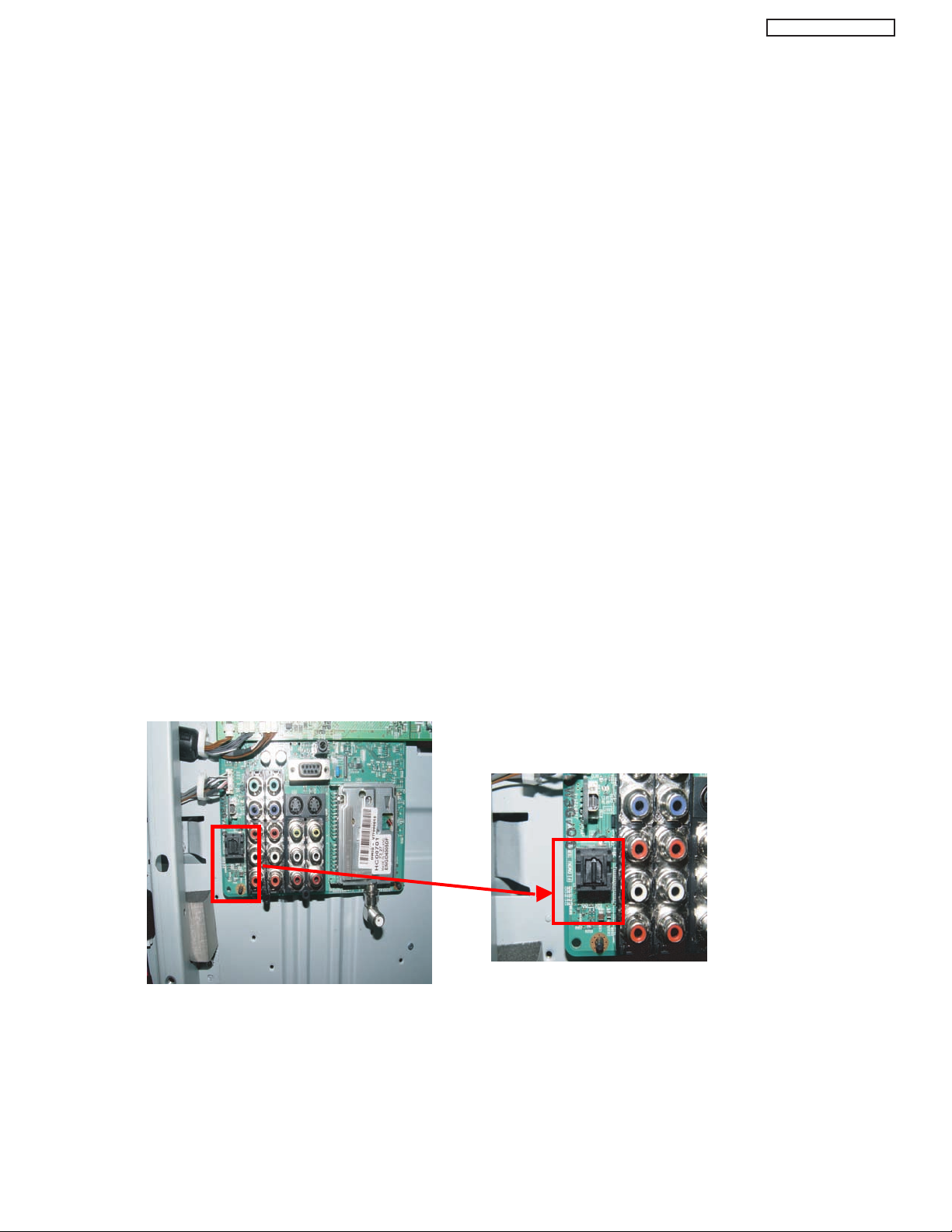
햹 For Special AV control use only.
햺
For Factory use only.
햻
Power Swivel Connector
Connect from here the Power Swivel cable (provided)
to the
Table Top Stand Base swivel slot.
22
DW3G
B
Page 24
23
DVI to HDMI
Cable
Connecting External Video Sources
The SIDE panel jacks are provided as a convenience to allow you to easily connect HDMI or DVI signals
from a DVD, Set Top Box , Video Game as shown in the following examples (When connecting DVI signal it will
need to connect the audio output into the side Audio Input jacks) :
A) Connecting HDMI signal.
SIDE INPUT PANEL
Note : Special device cables will be
according to the own device
specifications.
DW3G
B) Connecting DVI signal.
SIDE INPUT PANEL
Back of
HDTV Set-Top-Box or
DVD Player
OUTPUT CAPABILITY
DVD , Set Top Box,
Video Game Console.
DIGITAL OUTPUT
HDMI DIGITAL
AUDIO OUTPUT
R L
Note : Special device cables will be
according to the own device
specifications.
DVI DIGITAL
OUTPUT CAPABILITY
DVD , Set Top Box,
Video Game Console.
NOTE: 1. Completely insert connection cord plugs when connecting to side panel jacks. If you do not, the
played back picture may be abnormal.
Page 25
Connecting External Video Sources
The SIDE panel jacks are provided as a convenience to allow you to easily connect a camcorder , DVD, Video
Game and a VCR as shown in the following examples:
SIDE INPUT PANEL
Video Game
COMPOSITE VIDEO
OUTPUT CAPABILITY
DVD , Video Game
Console.
OUTPUT
R L
Video
DW3G
N
ote :For Monoaural devices, please
connect
Audio signal cable into
Video Camera
L/Mono input jack .
N
ote :Special device cables will
a
ccording to the own device
specifications.
NOTE:1. Completely insert connection cord plugs when connecting to side panel jacks. If you do not, the
played back picture may be abnormal.
The exact arrangement you use to connect the VCR, camcorder, laserdisc player, DVD player, or HDTVSet
Top Box to your LCD TV is dependent on the model and features of each component. Check the
owner’s manual of each component for the location of video and audio inputs and outputs.
The following connection diagrams are offered as suggestions. However, you may need to modify them to
accommodate your particular assortment of components and features. For best performance, video and
audio cables should be made from coaxial shielded wire.
Before Operating External Video Source
Connect an external source to one of the INPUT terminals, then press the INPUTS button to show the
INPUTS menu. Use the CURSOR PAD ( and ) to select the Input of your choice. Then press
the SELECT button or the CURSOR PAD to confirm your choice.
be
HDMI 2
HDMI-Front
Cable
Air /
Input 1
Input 2
Move SEL Sel.
24
Page 26
Rear Panel Connections
DW3G
DVD Player
/C
Y
P
B
OUTPUT
/C
P
R
B
OUTPUT CAPABILITY
AUDIO OUT
L R
R
DIGITAL
DIGITAL OUTPUT
DVI
to
HDMI
HDMI DIGITAL
OUTPUT CAPABILITY
HDMI OUTPUT
HDMI
to
HDMI
Optional
S-VIDEO
VCR #2
V L R
INPUT
Optional
Y P
P
L R
B
R
OUTPUT
HDTV Set-Top Box
NOTE: Cables are optional, except when specified.
S-VIDEO
OUTPUT
25
V L R
VCR #1
Outside
Antenna
or
Cable TV coaxial cable
ANT
IN
2-Way signal splitter
Page 27

Tips on Rear Panel Connections
•S-VIDEO, Y-PBPR, or HDMI connections are provided for high performance laserdisc players, VCRs etc. that
have this feature. Use these connections in place of the standard video connection if your device has this
feature.
If your device has only one audio output (mono sound), connect it to the left audio jack on (L/(MONO)) the
•
Rear Panel.
•Refer to the operating guide of your other electronic equipment for additional information on connecting
your hook-up cables.
•A single VCR can be used for VCR #1 and VCR #2, but note that a VCR cannot record its own video or line
output. Refer to your VCR operating guide for more information on
Connect only 1 component (VCR, DVD player, camcorder, etc.) to each input jack.
•
line input-output connections.
DW3G
•COMPONENT: Y-P
DVD players and set-top-boxes. Use these connections in place of the standard video connection if your
device has this featu
Your component outputs may be labeled Y, B-Y, and R-Y. In this case, connect the components B-Y
•
output to the TV
Your component outputs may be labeled Y-C
•
TV
It may be necessary to adjust TINT to obtain optimum picture quality when using the Y-P
•
To ensure no copyright infringement, the MONITOR OUT output will be abnormal, when using the
•
HDMI input jacks.
• Input HDMI 1, HDMI 2 or HDMI FRONT can accept HDMI signal.
• S-VIDEO monitor output may be used for recording only when the input is of S-VIDEO type.
• When using a HDMI input fr
•
When HDMI input a 1080p signal, it is recommended that the length of the cable be less than 5 meters.
INSTALLATION RECOMMENDATION:
1. Video signals fed through a VCR may be affected by copyright protection systems and the picture
will be distorted on the television.
2. Connecting the television directly to the Audio/Video output of a Set-Top-Box will assure a more
normal
input and the components CRoutput to the TV’s PRinput.
’s P
B
picture.
(Input 2 & 3) connections are provided for high performance components, such as
BPR
re.
’s P
input and the components R-Y output to the TV
B
. In this case, connect the components CBoutput to the
BCR
om a Set-Top-Box, it is recommended to use a 1080p, 1080i or 720p input signal.
’s P
R
input.
BPR
inputs.
BPR and
Y-P
26
Page 28
Back of
VCR
OUTPUT
VCR
Video
Connecting External Video Sources
CONNECTING A VIDEO AND STEREO AUDIO
SOURCE TO INPUT1 ~ INPUT-FRONT
1.Connect the cable from the VIDEO OUT of the
VCR or the laserdisc player to the INPUT
(VIDEO) jack, as shown on the Rear Panel to the
right.
2.Connect the cable from the AUDIO OUT R of the
VCR or the laserdisc player to the INPUT
(AUDIO/R) jack.
3.Connect the cable from the AUDIO OUT L of the
VCR or the laserdisc player to the INPUT
(AUDIO/L) jack.
4. Press the INPUTS button, then select INPUT 1
2,3 or Front from the INPUTS menu to view the
program from the VCR or laserdisc player.
5. Select CABLE or AIR from the INPUTS menu
or ANT key from the R/C to return to the last
channel tuned.
Cable or
Air signal
DW3G
NOTE:1.Completely insert the connection cord plugs when connecting to rear panel jacks. The picture and
sound that is played back will be abnormal if the connection is loose.
2.A single VCR can be used for VCR #1 and VCR #2 but note that a VCR cannot record its
own video or line output. Refer to your VCR operating guide for more information on line inputoutput connections.
3. When INPUT 2 or 3 are used, it is necessary to connect the video output of the device to the
Y/VIDEO input jack of the TV .
CONNECTING AN S-VIDEO AND STEREO AUDIO
SOURCE TO INPUT 1
1. Connect the cable from the S-VIDEO OUT of
the S-VHS VCR or the laserdisc player to the
INPUT (S-VIDEO) jack, as shown on the Rear
Panel to the right.
2. Connect the cable from the AUDIO OUT R of
the VCR or the laserdisc player to the INPUT
(AUDIO/R) jack.
3. Connect the cable from the AUDIO OUT L of
the VCR or the laserdisc player to the INPUT
(AUDIO/L) jack.
4.
Press the INPUTS button, then select INPUT 1
from the INPUTS menu to view the program
fr
om the VCR or laserdisc player.
5.
Select CABLE or AIR from the INPUTS menu
or ANT key from the R/C to return to the last
channel tuned.
Cable or
Air signal
Back of VCR or
Laserdisc Player
R L
VCR or Laserdisc Player
NOTE: 1. Completely insert the connection cord plugs when connecting to rear panel jacks. The picture and
sound that is played back will be abnormal if the connection is loose.
2.A single VCR can be used for VCR #1 and VCR #2, but note that a VCR cannot record
its own video or line output. Refer to your VCR operating guide for more information on line inputoutput connections.
27
Video
OUTPUT
S-VIDEO
Page 29

Connecting External Video Sources
DW3G
CONNECTING A COMPONENT SOURCE WITH HDMI OR
DVI CAPABILITY TO HDMI 1, HDMI 2 OR HDMI FRONT
1. Connect the HDMI or DVI to HDMI connection
cable from the output of the HDTV set top box
or DVD player to the HDMI input as shown
on the Rear panel below.
2. With DVI output, connect the cable from the
AUDIO OUT R of the HDTV set top box or DVD
player to the INPUT (AUDIO/R) jack as shown on
the Rear Panel below.
3. With DVI output, connect the cable from the
AUDIO OUT L of the HDTV set top box or DVD
player to the INPUT (AUDIO/L) jack as shown
on the Rear Panel below.
4. Press the INPUTS button, then select HDMI 1, 2
or FRONT to view the program from the HDTV
SET TOP BOX or DVD player.
5. Select CABLE or AIR from the INPUTS menu
or ANT key from the R/C to return to the last
channel viewed.
HDMI input
or
HDMI
able
C
DIGITAL OUTPUT
Back of
H
DTV Set-Top-Box or
DVD Player
NOTE: 1. Completely insert the connection cord
plugs when connecting to rear panel jacks.
The picture and sound that is played back
will be abnormal if the connection is loose.
2. The HDMI input on HDMI 1 , 2 and FRONT
contains the copy protection system called
High-bandwidth Digital Content Protection
(HDCP). HDCP is a cryptographic system
that encrypts video signals when using
HDMI connections to prevent illegal
copying of video contents.
3. HDMI is not a “NETWORK” technology. It
establishes a one-way point-to-point
connection for delivery of uncompressed
video to a display.
4.
The connected digital output device
controls the HDMI interface so proper set-up
of device user settings determines final
video appearance.
5. When using a DVI to HDMI cable, connect the
Audio Out L and R cables at the same INPUT
(1 , 2 or Front) as your HDMI INPUT(1 , 2 or Front).
HDTV Set-Top-Box or
DVD Player
DVI to HDMI Input
Back of HDTV
Set-Top-Box
or DVD Player
OUTPUT
L R
HDTV Set-Top-Box or
DVD Player
DIGITAL OUTPUT
DVI to HDMI
Cable
CABLE
or
Air signal
or
CABLE
or
Air signal
28
Page 30

Connecting External Audio/Video Devices
CABLE
or
Air signal
L
CONNECTING A COMPONENT AND STEREO
AUDIO SOURCE TO INPUT 2 or 3 :Y-PBPR.
DW3G
1. Connect the cable from the Y OUT of the
Laserdisc/DVD player or HDTV set top box to
the INPUT (Y) jack, as shown on the Rear
panel below.
2. Connect the cable from the PB/CBOUT or BY OUT of the Laserdisc/DVD player or HDTV
set top box to the INPUT (PB)jack.
3. Connect the cable from the PR/CROUT or RY OUT of the Laserdisc/DVD player or HDTV
set top box to the INPUT (PR) jack.
4. Connect the cable from the AUDIO OUT R of
the Laserdisc/DVD player or HDTV set top box
to the INPUT (AUDIO/R) jack.
5. Connect the cable from the AUDIO OUT L of
the Laserdisc/DVD player or HDTV set top box
to the INPUT (AUDIO/L) jack.
6. Press the INPUTS button, then select INPUT 2 or 3
from the INPUTS menu to view the program
from the Laserdisc/DVD player or HDTV set
top box.
Select CABLE, AIR or ANT key from the
7.
R/C to return to the last channel tuned.
NOTE: 1. Completely insert the connection cord
plugs when connecting to rear panel jacks.
The picture and sound that is played back
will be abnormal if the connection is loose.
29
AUDIO
R
Back of
DVD Player
OUTPUT
PR/CR PB/CB Y
DVD Player
IDEO
V
OR
OUTPUT
R Y P
L
HDTV Set-Top Box
B P
R
Page 31

Connecting External Audio/Video Devices
CONNECTING A VIDEO AND MONAURAL AUDIO
SOURCE TO INPUT 1 ~ FRONT INPUT
1. Connect the cable from the VIDEO OUT of the
VCR or the laserdisc player to the INPUT
(VIDEO) jack, as shown on the Rear Panel on the
right.
2. Connect the cable from the AUDIO OUT of the
VCR or the laserdisc player to the INPUT
(MONO)/L(AUDIO) jack.
3. Press the INPUTS button, then select INPUT 1
2,3 or Front from the INPUTS menu to view the
program from the VCR or the laserdisc player.
DW3G
4.Select CABLE or AIR from the INPUTS menu or
ANT key from the R/C to return to the previous channel.
CONNECTING AN EXTERNAL AUDIO AMPLIFIER
To monitor the audio level of the LCD TV to an
external audio amplifier, connect the system as
shown on the right. The “OPTICAL OUT” from the
Rear Panel is a fixed output. The Volume of the
amplifier is controlled by the amplifier, not
by the LCD Television. The OPTICAL OUT terminal
outputs all audio sources with Optical IN capability.
1. Connect an optical cable from the Optical out to
the Optical input of a separate Stereo System
Amplifier as shown on the Rear Panel on the
right.
CONNECTING MONITOR OUT
The MONITOR OUT terminal outputs video and
audio of CABLE/AIR and INPUTS 1, 2, 3 and Front.
It does not output component and HDMI video.
CABLE or Air signal
CABLE
or
Air signal
Back of
VCR
VIDEO OUT AUDIO OUT
OUTPUT
VCR
Stereo System Amplifier
OPTICAL
IN
Stereo System Amplifier
or DVD Player
1. Connecting S-Video:
Connect the cable from the S-VIDEO OUT of
the Rear Panel to the INPUT (S-VIDEO) jack, of
the VCR or Laserdisk player.
Connecting Video:
Connect the cable from the VIDEO INPUT of
the VCR or the laserdisc player to the VIDEO
out jack on the TV Rear Panel.
2. Connect the cable from the AUDIO IN R of the
VCR or the laserdisc player to the OUTPUT
(AUDIO/R) jack on the TV Rear Panel.
3. Connect the cable from the AUDIO IN L of the
VCR or the laserdisc player to the OUTPUT
(AUDIO/L) jack on the TV Rear Panel.
CABLE
or
Air signal
R L V
VCR or other external
components
NOTE: When making video connections, connect S-Video only or Video only. If both are connected, S-Video
takes priority.
30
Optional
INPUT
S-VIDEO
Page 32

TABLE OF CONTENTS OF ADJUSTMENTS
TO GO TO A SECTION, CLICK ON ITS HEADING BELOW.
1. Adjustment procedure start-up . . . . . . . . . . . . . . . . . . . . . . . . . . . . . . . . . . . . .
1.1. How to get into adjustment mode . . . . . . . . . . . . . . . . . . . . . . . . . . . . . . .
1.2. Changing data and selecting adjustment code . . . . . . . . . . . . . . . . . . . . .
2. Memory Initialize . . . . . . . . . . . . . . . . . . . . . . . . . . . . . . . . . . . . . . . . . . . . . . .
2.1. Memory Initialize operation . . . . . . . . . . . . . . . . . . . . . . . . . . . . . . . . . . .
2.2. Factory and service adjustments . . . . . . . . . . . . . . . . . . . . . . . . . . . . . . .
3. Video Adjustment
3.1. Sub-contrast and clamp adjustment . . . . . . . . . . . . . . . . . . . . . . . . . . . . .
4. White balance adjustment
4.1. Video Color Temperature adjustment (High) . . . . . . . . . . . . . . . . . . . . . . .
4.2. Video Color Temperature adjustment (Medium) . . . . . . . . . . . . . . . . . . . .
4.3. Video Color Temperature adjustment (Standard) . . . . . . . . . . . . . . . . . . .
4.4. Video Color Temperature adjustment (B&W) . . . . . . . . . . . . . . . . . . . . . .
5. Digital Main Check . . . . . . . . . . . . . . . . . . . . . . . . . . . . . . . . . . . . . . . . . . . . . .
6. Picture Check . . . . . . . . . . . . . . . . . . . . . . . . . . . . . . . . . . . . . . . . . . . . . . . . . .
7. Factory Reset . . . . . . . . . . . . . . . . . . . . . . . . . . . . . . . . . . . . . . . . . . . . . . . . . .
DW3G
32
32
32
32
32
33
33
34
34
35
35
35
36
36
TABLE OF CONTENTS
31
Page 33

1 ADJUSTMENT PROCEDURE START-UP
The L42S601 and the L42V651 LCD TV sets
pass through adjustment procedures during the assembly
process. These adjustments must be done to enssure the
best performance of the LCD set for the consumer.
Also, after servicing, these same adjustments must be
done. The adjustments are all made through the I
by changing data in the Adjustment mode menu.
1.1 HOW TO GET TO THE ADJUSTMENT MODE
Chassis adjustment modecan be accessed by pressing
the R/C keys MENU + MENU + 8 + SELECT to enter
adjustment mode. For some parameters the only way
to see them is by selecting the parameter number then
press SELECT in order to see it; then DATA can be
changedif other parameter needs to change then press
key then repeat the same procedure.
ADJUST MODE
FACT RESET
MEMORY INIT
RGB
WHITE BAL HIGH
WHITE BAL MED
WHITE BAL STD
WHITE BAL B/W
2
C bus
DW3G
Side Panel control
B. To make a selection, use the NUMBERpad on the LCD
R/C ; example: selectDEVICE press 69 then SELECT
the DATA shown is "EB"; if this DATA needs to be changed
press the keys to modify, when finish press SELECT
, ,
key to store the new DATA value.
normal condition.
C. After finishing the necessary adjustment press the R/C
EXIT key or EXIT key on the side panel.
Adjustment mode is released and LCD set returns to
normal condition.
Other way to access this mode is by use JIG R/C code: (9C Hex).
To escape from Adjustment Mode press “INPUT” key on Side
panel or EXIT key of R/C to exit service adjustment mode.
1.3 CHANGING DATAAND SELECTING ADJUSTMENT
CODE
When the LCD set is in adjustment mode, the cursor , ,
, and MENU keys of the remote control or side panel
may be used as the adjustment keys.
A. Use any Hitachi remote control when making an
adjustment.
, keys are used for selecting adjustment item.
, keys are used for changing data values.
MENU key is used to advance through the adjustment
mode menus and pages.
2 MEMORYINITIALIZE
2.1 MEMORYINITIALIZEOPERATION
NOTE: The execution of this function returns the
adjustment codes to the preset values, therefore,
adjustment data will be lost.
Procedure
(1) Enter Adjustment mode by the method described in
sub-items 1.1 and 1.2 from item 1 (“Adjustment
procedure start up”).
(2) Get to the second row of Adjust Mode by pressing
R/C or side panel
cursor key once.
(3) Select MEMORY INIT adjust code.
(4) Activate MEMORY INIT by pressing
cursor key for
more than 3 seconds.
(5) Check the following process for initialization opera-
tion.
Part of S and V models remote control keys.
*Note:PIP key(V Models), ANT key(S models)
BACK TO ADJUSTMENTS
32
Page 34

2.1 Process of Memory Initialize operation.
①
The screen is colored blue when MEMORY INIT
start.
The screen is colored green when MEMORY INIT
②
finish normally.
The screen is colored redwhen MEMORY INIT
③
finish abnormally.
(6) Do not unplug from AC outlet until this operation
is complete and do not perform any key operation
either, after this operation each factory setting and
all adjust mode data should reset to delivery settings
automatically.
(7) After Memory Initialize, the AC cord should be un-
plugged. Unplug and plug the AC cord and then all
settings and data will be updated.
(8) When LCD turns ON , it will tune CH03 this is the
complete operation of Memory Initialize process.
2.2 FACTORY AND SERVICE ADJUSTMENTS
The adjustment item that is affected by the memory
initialize operation is shown below:
ITEM
WHITE BALANCE
ADJUSTMENT
DATA
SUB CONTRAST
ADJUSTMENT
DATA
CLAMP OFFSET
ADJUSTMENT
DATA
OTHER
ADJUSTMENT MODE
DATA
RESET
Y
OR
ACT
F
MEMORY
INITIALIZE
NOT
INITIALIZED
NOT
INITIALIZED
NOT
INITIALIZED
INITIALIZED
INITIALIZED NOT
PROTECTION
DATA
INITIALIZED
INITIALIZED
INITIALIZED
NOT
INITIALIZED
INITIALIZED
FACTORY
RESET
NOT
INITIALIZED
NOT
INITIALIZED
NOT
INITIALIZED
NOT
INITIALIZED
INITIALIZED
MMC
SOFTWARE
UPGRADE
NOT
INITIALIZED
NOT
INITIALIZED
NOT
INITIALIZED
NOT
INITIALIZED
NOT
INITIALIZED
BECKHAM
SOFTWARE
UPGRADE
INITIALIZED
INITIALIZED
INITIALIZED
INITIALIZED
INITIALIZED
DW3G
Note: Perform pre heat-run for more than 20 min. before
adjusting.
3 Sub-Contrast Adjustment
Preparation for adjustment
(1) Pre-heat at least 2 min. before the adjustment.
(2) Recall user menu and select ‘Video’ඎ ‘Picture Mode’ඎ
‘Day(Dynamic)’ඎ ‘Reset’.
(3) Receive following signal into input3 or input4(Comp) input.
Adjustment procedure
3.1 525p Sub-Contrast, Y/Cb/Cr Clamp offset adjustment
(1) Receive following 525(480)p Signal.
100% White
V2 V1
Black
Black White
Format : 525(480)p
Adjustment signal for 525(480)p format
(2) Go into Service Adj. Menu and select ‘RGB’ .
(3)
Press for over 2 seconds and the TV will do
automatic adjustment. When it’s completed, the
OSD will appear, during adjustment, it will disappear.
BACK TO ADJUSTMENTS
V1=1Vpp
V2=0.7Vpp
33
Page 35

DW3G
4 WHITE BALANCE ADJUSTMENTS
General Notes for White Balance
(1) If the incident illumination is more than 20 lux,
change the environment (location, lighting, etc.) and
ensure it to be less than 20 lux.
(2) At least one of the color drive codes must stay at its
default value, 110.
4.1 VIDEO COLOR TEMPERATURE ADJUSTMENT
(HIGH)
Preparation 1
(1) Set the output of signal generator to white raster.
(Ratio:100%)
(2) Component signal (480i)
Video level: 0.700Vp-p
SYNC: 0.300Vp-p
Set-up level: 0V
(3) Input white raster signal into COMPONENT input
terminal of the LCD set.
(4) Set user control to Day(Dynamic) mode. (Picture Mode)
(5) Confirm that the mode is set as “Factory Setting
Mode”.
(6) Aspect: 4:3 Expanded
(7) Allow at least 20 minutes heat-run before adjusting.
Remarks
(1) Color temperature should be adjusted under the
condition in which the screen is the brightest, thus
the initial value for adjustment is set to its maximum.
(2) Adjustment is made by reducing brightness only.
Reduce a bright color for adjustment.
(3) Video color temperature & Adjustment no. are the
same, but addresses in the memory are different,
thus there’s no problem.
4.2 VIDEO COLOR TEMPERATURE ADJUSTMENT
(MEDIUM)
Preparation
(1) Same as “Video Color Temperature adjustment:
(HIGH)”.
Adjustment
(1) Perform the following adjustment with the remote
control.
(2) Set the CRT color analyzer (non contact type: CA-210,
BM-5, BM-7, CA-110) at the center of the panel.
(3) Set color temperature to “MEDIUM”.
(4) Ensure that Adjustment R/G/B DRIVE (MEDIUM) are
all set as 110.
(5) After receiving White raster signal, reduce the value
of two (or only one) of the adjustment parameters
R/G/B DRIVE (MEDIUM) and adjust to the target value
shown below.
Adjustment
(1) Perform the following adjustment with the remote
control.
(2) Set the CRT color analyzer (non contact type: CA-210,
BM-5, BM-7, CA-110) at the center of the panel.
(3) Set color temperature to “HIGH”.
(4) Ensure that Adjustment R/G/B DRIVE (HIGH) are all
set as 110.
(5) After receiving the White raster signal, reduce the value
of two (or only one) of the adjustment parameters
R/G/B DRIVE (HIGH) and adjust to the target value
shown below.
Specification
Video Color temperature (HIGH)
x = 0.273 ± 0.005
y = 0.273 ± 0.005
(Color temp: 12000K-7MPCD)
At least one of the data should be 110.
Specification
Video Color temperature (MED)
x = 0.285 ± 0.005
y = 0.293 ± 0.005
(Color temp: 9300K)
At least one of the data should be 110.
Remarks
(1) Color temperature should be adjusted under the
condition in which the screen is the brightest, thus
the initial value for adjustment is set to its maximum.
(2) Adjustment is made by reducing brightness only
Reduce a bright color for adjustment.
(3) Video color temperature &
same, but addresses in the memory are different,
thus there’
s no problem.
Adjustment no. are the
.
BACK TO ADJUSTMENTS
34
Page 36

DW3U
the MMC/SD card with the new software.
4.3 VIDEO COLOR TEMPERATURE ADJUSTMENT
(STD)
Preparation
(1) Same as “Video Color Temperature adjustment: (HIGH)”.
Adjustment
(1) Perform the following adjustment with the remote
control.
(2) Set the CRT color analyzer (non contact type: CA-210,
BM-5, BM-7, CA-110) at the center of the panel.
(3) Set color temperature to “STANDARD”.
(4) Ensure that Adjustment R/G/B DRIVE (STD) are all
set as 110.
(5) After receiving the White raster signal, reduce the
value of two (or only one) of the adjustment
parameters R/G/B DRIVE (STD) and adjust to the
target value shown below.
Specification
Video Color temperature (STD)
x = 0.314 ± 0.005
y = 0.323 ± 0.005
(Color temp: 6500K )
At least one of the data should be 110.
Remarks
(1) Color temperature should be adjusted under the
condition in which the screen is the brightest, thus
the initial value for adjustment is set to its maximum.
(2) Adjustment is made by reducing brightness only.
Reduce a bright color for adjustment.
(3) V
ideo color temperature & Adjustment no. are the
same, but addresses in the memory are different,
thus there’s no problem.
4.4 VIDEO COLOR TEMPERATURE ADJUSTMENT
(B/W)
Preparation
(1) Same as “Video Color Temperature adjustment:
(HIGH)”.
Adjustment
(1) Perform the following adjustment with the remote
control.
(2) Set the CRT color analyzer (non contact type: CA-210,
BM-5, BM-7, CA-110) at the center of the panel.
(3) Ensure that Adjustment R/G/B DRIVE (B/W) are all
set as 1
10.
(4) After receiving the White Raster signal, reduce the
value of two (or only one) of the adjustment
parameters R/G/B DRIVE (B/W) and adjust to the
target value shown below.
Specification
Video Color temperature (B/W)
x = 0.335 ± 0.005
y = 0.343 ± 0.005
(Color temp: 5400K )
At least one of the data should be 110.
Remarks
(1) Color temperature should be adjusted under the
condition in which the screen is the brightest, thus
the initial value for adjustment is set to its maximum.
(2) Adjustment is made by reducing brightness only.
Reduce a bright color for adjustment.
(3) Video color temperature & Adjustment no. are the
same, but addresses in the memory are different,
thus there’s no problem.
DIGITAL MAIN CHECK
5.
5.1
SYSTEM SOFTWARE VERSION CHECK
(1) Press Menu button on the R/C or control
panel.
(2) Enter the SETUP options, and then look
for UPGRADES option.
(3) The Main software version will be display
Vxxx.xxxx as shown on Fig. 1.
(4) If this version needs to be changed for a
design improvement or failure, please
select the Upgrade Now button after inserting.
Fig. 1
Setup
OR
Pl
ease Insert MMCcard
ove Return
Reset The Software
Software Version # : Main Vxxxx.xxxx
MMC Software Upgrade
Upgrade Now
Please Insert MMC card before upgrading.
Reset TV Settings
(Select "Yes" to return all settings to the factory
default after main power OFF/ON.)
Move
SEL Return
No Yes
Software Version
(5) The upgrading process begin by filling a
bar, when finish the message will say,
“U
pgrade complete …” when this appea
r
unplug the TV from the AC line outlet to
complete the process.
(6) Now plug again the TV and verify the
new software version.
(7) The Main software version will display the
latest version issued by Hitachi.
NOTE:
(1
) Always check the service website for
the latest software upgrade version.
www.hitachiserviceusa.com.
(2) In case that the upgrade fails or when a
CARD is inserted with new version and
can’t upgrade ; pl
ease perform the
FACTORY RESET process to the TV,
then try upgrading again.
BACK TO ADJUSTMENTS
35
Page 37

DW3G
6. PICTURE CHECK
Preparation
(1) Set AC120±1V.
(2) Turn on the power and leave it more than 5 min.
(3) Input 480p and 1080i circle pattern into Component
video 3. (ASPECT 16:9 Standard)
Checking
(1) Receive 480p and 1080i signal, then check
the following items 1~4:
1. Check the symmetry of the pattern (right/left).
2. Check the horizontal position and the balance
(right/left).
3. Check the symmetry of the pattern (top/bottom).
4. Check the vertical position and the balance
(top/bottom).
3
7. FACTORY RESET
After all of the adjustments of main chassis are finished,
perform FACTORY RESET.
(1) Enter Adjustment Mode by the method described in
sub-item 1-1 from page 32. (“Adjustment Procedure
Start-up”).
(2) From the first menu in Adjustment Mode, select
FACT RESET adjustment code.
(3) Activate FACT RESET by pressing “Right” cursor
key for more than 3 seconds.
(4) Other procedure to acces the FACTORY RESET is by
sending the 92 hex code with a programable R/C.
(5) The procedure of the FACTORY RESET process is
the following and the DATA table is shown next.
·Process of FACTORY RESET operation.
①
The screen is colored magenta when FACTORY
RESET start.
The screen is colored green when FACTORY
②
RESET finish normally.
The screen is colored RED when FACTORY
③
RESET finish abnormally.
(6) After FACTORY RESET, the AC cord should be
unplugged. Unplug and plug AC cord and then all
settings and data will be updated.
(7) When the LCD turns ON, it will tune CH03 this is the
complete
operation of FACTORY RESET process.
Remarks
A B
SCREEN
0 1 2 2 1 0
SIGNAL ASPECT SPEC(A,B)
Hitachi circle pattern 16:9 Standard1 0 +/- 0.5
BACK TO ADJUSTMENTS
36
Page 38

LCD Panel Module troubleshooting.
DW3G
TROUBLE-SHOOTING FLOW CHARTS
No picture, no color or dark
Is Backlight
Unit lighted?
No Yes Yes
Yes No No
Check Panel Module except Inverter PWB
Are voltages
at Pin1〜2 of CN203
+12V?
Is voltage
at Pin5 of CN203
High level?
Check Main-Digital board
Are voltages
at Pin1〜5 of CN201andCN202
+24V?
Is there voltage
at Pin6 of CN203?
Yes
Check Inverter PWB
No Yes
No
Is there voltage
at Pin7 of CN101?
No Yes
Are voltages
at Pinn 1~3 of CN204
+5.6V?
Yes
No
Check Power Supply Unit
No
Is there voltage
at Pin6 of CN101?
Yes
Check Main-Digital board
TABLE OF CONTENTS
37
Page 39

Y
p
Y
Y
Y
TROUBLE-SHOOTING FLOW CHARTS
Terminal PWB circuit troubleshooting
DW3G
No picture, no color or dark
Analog format signal
NTSC, composite, s, component
Q013-E(Y), Q012-E(PB) and Q011-E(PR)
Are waveforms at
OK?
No
Component video input
osite video input
Com
Are waveforms at
pin73/67(Y), 71/65(PB) 69/63(PR)
pin10/22/53(CV) pin14(Y), 12(C)
of I001 OK?
No
Digital format signal
es
Check Main-Digital board
es
Check I001
HDMI Cable/Air
A
Cable/Air
es
Are waveform at
pin26(CV) of I001 OK?
No
Check Input terminal
Check UT01 (Tuner)
es
Are waveforms at
pin 9(SDA), 10(SCL) and
voltage at pin 2/7/18/20(+5V)
of UT01 OK?
No
Check IT06, IT07
or Main-Digital board
38
Page 40

Y
Y
Y
Y
Y
Y
TROUBLE-SHOOTING FLOW CHARTS
…Terminal circuit Troubleshooting diagram continued.
DW3G
A
Follow next procedure:
(1) Select ‘Maintenance’ of Adjustment mode menu.
(2) Press SELECT. (while ‘<Display>’ at “Front End” lights yellow.)
(3) Check the indication of ‘Frame/MPEG Lock’ line.
Is the indication
[LOCK] ?
No
Check UT01 (Tuner)
es
No sound, abnormal sound
Are waveforms at
terminals of speaker
OK?
No
es
Check Speaker
Check Main-Digital board
Cable/Air, Input 1/2/3/Front HDMI
Cable/Air
Are waveforms at
pin 1(L) and pin 4(R) of Q002
OK?
No
Input 1/2/3/Front
Are waveforms at
pin 91/89/87/85(L) and
pin 92/90/88/86(R) of I001
OK?
No
Check Input terminal
es
Check Main-Digital board
es
Check I001
es
es
Check UT01 (Tuner)
Are waveforms at
pin 83(L) and
pin 84(R) of I001
OK?
No
Are waveforms at
pin 9(SDA), 10(SCL) and
voltage at pin 2, 7, 18(+5V)
of UT01 OK?
No
Check IT06, IT07
or Main-Digital board
39
Page 41

Y
Y
Y
Y
Power Supply troubleshooting
DW3G
TROUBLESHOOTING FLOW CHARTS
(No picture, and No sound)
No Power
Is Power Indicator
orange lighted?
No
Is Power Indicator
not lighted?
es
Power Indicator
blue is lighted normally.
Does Power Supply Unit output
+10V/16.5V/13V/24V?
No
Check Power Supply Unit. (*)
Video Power Save Mode
es
(Input:1~3, Front)
No
es
Does Power Supply Unit
Check Power Supply Unit. (* and Fuse
or AC-Inlet / Connector)
Check Main-Digital board
output +5.6V?
No
or Terminal PWB
es
Check Main-Digital board.
(*) Power-On control signal for Power Supply Unit
(1) Power connected : ON Æ PSU outputs STBY+5V.
(2) PoWER_1 (CN101 [6]) : High Æ PSU outputs +5.6V.
(3) PoWER_2 (CN101 [7]) : High Æ PSU output +10V,16.5V, audio 13V and 24V.
If any control signal does not rise, PSU cannot output the voltage.
・PoWER_1/2 : not rise ----- Main-Digital PWB trouble
40
Page 42

A
A
AC
Inlet
Remote
Control
Speaker R
DW3G
BLOCK DIAGRAM
For L42V651 and L42S601
TFT
Module
Timing
Converter
DC/DC
Converter
LVDS
Receiver
Gate Driver
Back light unit
(Master)
LCD
Panel
Back light Inverter
Module
RGB
Power
Blon
BRT
(LVDS)
Supply
IR
Receiver
LED PWB
Unit
C-CLK
Power2
Power1
LED
Key
SW
Control PWB
BLoN
DoN
VLC
BRT
Main-Digital PWB
Sub
Micro
Seine2
A-chip
Audio
DSP
Audio
PWM
A/V
Pin Jack
PLD
(Nereid)
Seine2
D-chip
DDR2
Digital
Audio
Amplifier
Terminal PWB
DC-DC
Conv.
VCXO
PLL
Audio
DC
Audio
DAC
HDMI
HDMI
I/F
SD PWB
SD/MMC
Card I/F
Stand
Demodulator
UEI
IR-Blaster
Digital/
Analog
Tuner
Video
SW
Driver
Motor
Driver
Drain Driver
Lamp
・
・
・
Audio
A/V
Pin Jack
OPT-Audio
SW
RS-232C
Output
(Slave)
Back light Inverter
Speaker L
TABLE OF CONTENTS
41
Page 43

DS101
+
〜−〜
N/F
1
2
AC(N)
CN1
AC(L)
L301 L302
C301
TH1
F1
8A 125V
C302
C303
R301
R302
R303
Q301
Q302
Q303
D301
IC301
R313
R314
R315
R316
R317
R321
R322
R318
R319
R320
Q307
IC101
BLOCK DIAGRAM
DW3G
POWER SUPPLY BOARD
L42S601 and L42V651
F201
T4A 250V
Q201
+
C201
C202
C203
Q202
R208
R209
T201
●
C205
PC105
IC201
PC104
PC103
Q103
Q102
Q104
F101
T1A 250V
D102
+
C109
D104
ZD102
R112
C110
T101
●
●
PC102
PC101
RY101
D208, D209
●
D210, D211
●
+
C217
DC/DC
+
C227
R266
R267
REG.
R258
R259
D218 R257
R256
24V
13V
16.5V
GND
D212
D223
REG.
D219
R264
R265
D222
●
●
+
C220
REG.
D220
R260
R261
R262
R263
D221
10.5V
12V
VLCD_ON
POWER-2
AC_CLOCK
AC_Clock circuit Power_Off circuit
D106
D105
●
+
C114
D110 R132
Q207
R131
POWER_OFF
STB5V
5.6V
POWER-1
FGS1
42
Page 44

HDMI
USB 2.0
ANTENNA
CABLE
IR OUT
RS232C
G-LINK
Video 1 In
(Y-C-V / L/R)
Video 2 In
(Y-Pr-Pb / V / L/R)
Video 3 In
(Y-Pr-Pb / V / L/R)
Video 4 In
(Y-C-V / L/R)
Monitor Out
(n/a)
FAN
Swivel
OPT Out
SD CARD
or MMC
Upgrade Software
DDC ROM
IH03
IH04, IH05
(P50X901, P60X901, P50V701) only
TS
POD
CableCard
Switch
Oberon2
Digital/Analog Tuner (US)
VP12HSR
UT01
OOB Tuner
(Out of Band)
RS232C
S to P
IW01
IY03MAX202
IY02IY01
TERMINAL PWB
Monitor (Y-C-V)
Monitor Audio Out (L/R)
Fan Not Used
Fan Control
TK73400
IP03
PTW
Motor Driver
BA6287F
Optical Audio
DW-3 DIGITAL MODULE
BLOCK DIAGRAM
VSB/QAM
Demodulator
T314/T312
Video 1 - 3 (Y Pr / Pb / Y-C-V)
Video 1 - 3 Audio in (L / R)
Video 4 in (Y C/V)
Video 4 Audio in (L/R)
IP05
CH3
SD
HDMI SIDE
IT02
25.14Meg
POD (Not Used)
(P50X901, P60X901, P50V701)
Tuner-Main Video
Tuner-Main L/R Audio
IR BLASTER
9DR32DW8
Plasma Models Only
Main L/R
Sub L/R
SD Y/C
5V to 3.3V
Level Shifter
IM01
I001
CableCard
Video SW
Audio SW
R2S11007
IL01
Swivel Motor Drive
Optical Audio
MUTE
HDMI-2
HDMI-1
PMS1 to PSM
PNL-ON
TS0
MPEG (6:0)
MPEG (7:0)
SBCLK
RESET1
CRX, DRX
POWEROFF
I2C0
MAIN L/R
SUB L/R
TUNER RESET
I2C1
MUTE
Sub Y/V
PNL-ON
FAN DET
TV AFC
RS232C
Swivel
POWER OFF
SD Y, C
AEP L, R
ASP L, R
+10.5V
+5.6V
SBY +5V
Power Off
POWER2
POWER1
AC Clock
EC01
- 29
40
- 13
24
PNLRST
43
42
Enable
POWER 2_Td
FC8 (27Meg)
I2C1
PSPK
+13V
+16V
DCR
GK01671
GK01671
POWER SUPPLY
Pins
13,14,15
CN04
Pin 9
Pin 7
Pin 1,2,3
PSU
Pin 1
CN101
Pin 4
Pin 7
Pin 6
Pin 5
Pin 48 and 51
VLCD
T-CON
Back Light Brightnes
TA1-TE1
TA2-TE2
Pin 9 Not Used
Pin 10 (DCR Enable)
FC8
DDR2 SDRAM
256Mbit X 3
333MHz
FC8
RESET2
DC/DC
TPS54310
DC/DC
TPS54310
AC
IN
AC
CN1
INLET
PWB
PANEL
Logic PWB
(Pins 12 through 23)
(Pins 28 through 39)
NOTE
SBY Pow Block
+12V Pow Block
+10V Pow Block
+5.6V Pow Block
Power Line
Power Control
Clock
Reset 1, 2
SWITCH
CXB1441
I405
PI4C3390
I403
Regulator
TK73650
I2U1
DELAY
HDMI (L/R)
SW
SRC
AK4121
IF01
Audio ADC
PCM1808
IF02
Audio ADC
PCM1808
IF03
POWER1
QH01-QH04
IG06, IG07
3DYC
LVDS
TX
42MHz
18.432MHz
18.432M
18.432M
POWER 2_Td
HDMI
Main V
Main SY
Main Y
Main C
Main Pb
Main Pr
RESET 2
Sub CPU
M306H5
IH01
Switch
I901
CLAMP
CLAMP
CLAMP
RX
DDC
GCA
ADC
ADC
ADC
ADC
SYNC
SW 5V to 3.3V
(Level Shifter)
RESET1-IN
Key ROM
TC9K111 I406
TS0
TS3
RESET 1
LAN Initialize
G-TXD, G-RXD
UEI
SYNC SEP
SYNC SEP
UEI
MDM-DCD, RESET
FACTOR USE ONLY "FLASH"
BECKHAM PVM
FLASH
One NAND
Max 64Mb
I103
LVDS/Video (Single)
LVDS/Video (Duel)
LVTTL/Video
Switch
IF09
OneNAND
assist
RESET
MUTE
I/O
SW
POWER 2
SYS-REST
S-REST
PNL-REST
DSP-REST
SBCLK (66M)
I2C2
UART0
I2C0
I2C1
UART3
PNL-On
UART1
UART2
PCI
LVDS
RX
TX49H4
333MHz
IRQ
TSP
Peripheral
EXTB
POD
JTAG
DDR2 SDRAM
512Mbit X 4
333MHz
DDRC
CARD
PLL (20Meg)
I301-I304
CY2305C
SD
DVC
DVC
ASP
AEP
VCR
out
SYSRST
I106
PWM
CG
MAIN L/R
SUB L/R
OPT
I107
LVDS
TX
DAC
RESET
I104
PWM to DC
Regulator
TK11125CS
LVDS (Single)
LVDS (Duel)
LPF
PWM
SD CLK (54Meg)
USB (48Meg)
Audio (36.864Meg)
Audio (18.432Meg)
PCI CLK
CY2305C
IE04
iLink (27Meg)
PWM
SD CLK 54Meg
HD CLOCK
54.054Meg
Audio
Switch
IF04
36.864Meg
IC02
D+1.8V
D+1.3V
D+3.3V
CY22391-03
IE01
SS
CY22388
IE02
SW
SS
CY24900
IE06
Audio
DSP
NJU26040
IF05
DC/DC
MP2361
IG03
DC/DC
MP2361
IG01
DC/DC
TPS54310
IG02
Only High momentarily when AC removed
POWER 2_Td
LAMPCNT
27Meg
VCX0
PLL (54Meg)
PLL (48Meg)
PLL (54.054Meg)
PLL (36.864Meg)
PLL (18.432Meg)
PLL (24.576Meg)
IE03
CY24902
PLL (33.333Meg)
27Meg
VCXO
PLL (20Meg)
PLL (54Meg)
PLL (54.054Meg)
Switch
IE07, IE08
PLL (39.9875M)
PLL (74.9875M)
PLL (79.7142M)
PLL (79.9750M)
PLL (54.054M)
PWM
TAS5086
IF06
Audio DAC
WM8620
IF12
Audio DAC
WM8620
IF13
IE05
CY24901
10.5V
Digital
AMP
TAS5142
IF07
13V
16V
Delay
IG06
PPM3
Pins 4, 5, 6
PPM2
I2C2
PPM1
Others
ASP, AEP-RESET
(10Meg)
BACK TO CHANGE PAGE
Audio / Opt
42-A
S / PDIF
MUTE
TC7SZ125FU IF20
LED
IR
Key
PSL PSC
PLS
PCST
LED PWB
CONTROL PWB
LED
IR
Key
Page 45

CONNECTIONS DIAGRAM
L42S601 and L42V651
CH3
DW3G
CONNECTION DIAGRAM
AC INLET
N
AC IN
L
FG
POWER SUPPLY UNIT
Power PWB
CN1
1
2
Swivel PWB
SWIVEL PWB
SWIVEL PWB
Control PWB
CONTROL PWB
CONTROL PWB
PCST
GH-14V
V4-CY
GND
V4-Y
GND
V4-C
GND
V4-L
V4-R
GND
T+9V
PWRKEY
ADKEY0
ADKEY1
GND
PTW
52418-05HS-D
GND
MOTOR +
MOTOR JOINT DET
SW COM
PCST
GH-14V
1
2
3
4
5
1
2
3
4
5
6
7
8
9
10
11
12
13
14
VT-2P
1
AC (Neutral)
2
AC (Live)
TERMINAL PWB
Terminal PWB
PTW
53290-05VP-D
GND
1
MOTOR +
2
3
MOTOR -
4
JOINT DET
5
SW COM
Terminal PWB
PTC
GH-10V
1
V4-CY
2
GND
3
V4-Y
4
GND
5
V4-C
6
GND
7
V4-L
8
V4-R
9
GND
10
T+9V
LED PWB
LED PWB
LED PWB
VBL +24V
VBL +24V
VBL +24V
VBL +24V
VBL +24V
GND
GND
GND
GND
GND
VBR-A (N.C.)
V ON/OFF
VBR-B
STATUS (N.C.)
VBL +24V
Power PWB
VBL +24V
VBL +24V
VBL +24V
VBL +24V
GND
GND
GND
GND
GND
(N.C.)
(N.C.)
STBY +5V
GND
N.C.
POWER OFF
AC CLOCK
POD STB
REC STB
N.C.
CNPPS
EH-15P
+5.6V
+5.6V
+5.6V
GND
GND
Power PWB
GND
+10.5V
GND
+16V
GND
GND
GND
+13V
+13V
+13V
+12V
+12V
GND
GND
VLCD ON
BL ON
BRT
VBL ON (N.C.)
GND
PLS
501331-11V
501331-11V
iR iN
SBTBY+3.3V
iR-CAPiN
GND
+5.6V
SBTBY+5V
ALARM LED 0
PWR LED 0
PWR LED 1
M LED Green
M LED Red
CN201
PH-14P
1
2
3
4
5
6
7
8
9
10
11
12
13
14
CN202
PH-12P
1
2
3
4
5
6
7
8
9
10
11
12
CN101
EH-8P
1
2
3
4
5
6
7
8
CN204
EH-15P
1
2
3
4
5
6
7
8
9
10
11
12
13
14
15
CN203
PH-9P
1
2
3
4
5
6
7
8
9
1
3
5
7
9
11
13
15
17
19
21
23
25
27
29
31
33
35
37
39
41
43
45
47
49
51
53
55
57
59
61
63
65
67
69
71
73
75
77
79
81
83
85
87
Terminal PWB
89
91
93
95
97
99
101
103
105
107
109
111
113
115
117
119
121
123
125
127
129
131
133
135
137
139
141
143
145
147
149
151
153
155
157
159
PLS
1
2
3
4
5
6
7
8
9
10
11
PSM
501497-160VS
GND
+5.6V
+5.6V
+5.6V
+5.6V
GND
SBY +5V
GND
+16V
GND
No Connection
iR Out
No Connection
No Connection
F iN
R iN
CPDET
Swivel DET
GND
AEP-R
AEP-L
GND
ASP-R
ASP-L
GND
No Connection
GND
SEL-L-S
SEL-R-S
GND
SCL1 (3V) 100
SDA1 (3V) 100
GND
SCL Tuner
SDA Tuner
Analog/Digital
GND
IF AGC
GND
FDC AGC
GND
FAT INP
GND
GND
FAT INN
GND
FDC INP
GND
FDC INN
GND
FS OUTPUT
GND
POWER OFF
GND
FS OUTN
GND
GND
FAN DET
GND
MTV AFC
SIG DET
No Connection
PNLoN
GND
REC MUTE
GND
No Connection
No Connection
GND
No Connection
No Connection
No Connection
No Connection
No Connection
No Connection
No Connection
No Connection
GND
No Connection
GND
MAIN DIGITAL PWB
PPM1
ZH-08P
1
STBY +5V
2
GND
3
N.C.
4
POWER OFF
5
AC CLOCK
6
POWER 1
POWER 2
7
8
PNL ON
PPM2
PPM2
DF3D-15H
DF3D-15H
+5.6V
1
+5.6V
2
+5.6V
3
4
GND
GND
5
GND
6
+10.5V
7
GND
8
+16V
9
GND
10
GND
11
GND
12
N.C.
13
N.C.
14
N.C.
15
PPM2
PPM2
PPM2
PPM3
DF3D-15H
DF3D-15H
DF3D-15H
PA-6V
1
GND
GND
2
3
GND
4
+13V
5
+13V
6
+13V
EC02
ZH-09H
+12V (VDD)
1
2
+12V (VDD)
GND
3
4
GND
5
PNL ON
6
BL ON
7
-PWM
8
VBL ON (N.C.)
GND
9
PMS1
501493-160VP
GND
D +3.3V
D +3.3V
D +3.3V
GND
GND
SBY +3.3V
GND
+10V
SWIVEL-G
MAIN (Y/V)
GND
MAIN (Y/E)
GND
MAIN (Pb)
GND
MAIN (Pr/C)
GND
SUB (Y/V)
GND
S/PDiT
GND
SD Yo
GND
SD Co
GND
FAN Enable
No Connection
GND
No Connection
No Connection
GND
No Connection
No Connection
GND
SEL-L-M
SEL-R-M
GND
UATXD3
UARXD3
GND
SDA2-(3V)-100
GND
SCL2-(3V)-100
GND
No Connection
No Connection
POWER 2 Td
No Connection
GND
FAN CONTROL
No Connection
GND
No Connection
No Connection
No Connection
No Connection
GND
No Connection
GND
No Connection
GND
No Connection
GND
No Connection
GND
No Connection
GND
AVCTXD
AVCRXD
AVCCTS_N
AVCRTS_N
GND
No Connection
No Connection
No Connection
No Connection
No Connection
No Connection
No Connection
PSC
GH-04H
1
PWRKEY
2
ADKEY0
3
ADKEY1
4
GND
Digi-Main PWB
PSL
501568-11H
iR iN
1
2
SBTBY+3.3V
3
iR-CAPiN
4
GND
5
+5.6V
6
SBTBY+5V
ALARM LED 0
7
PWR LED 0
8
9
PWR LED 1
M LED G_N
10
M LED R_N
11
2
4
6
8
10
12
14
16
18
20
22
24
26
28
30
32
34
36
38
40
42
44
46
48
50
52
54
56
58
60
62
64
66
68
70
72
74
76
78
80
82
84
86
88
90
92
94
96
98
100
102
104
106
108
110
112
114
116
118
120
122
124
126
128
130
132
134
136
138
140
142
144
146
148
150
152
154
156
158
160
Digi-Main PWBDigi-Main PWBDigi-Main PWB
GND
N.C.
N.C.
N.C.
N.C.
N.C.
VLDS Select
N.C.
N.C.
(Low-level)
DCR Enable
GND
TA1TA1+
TB1TB1+
TC1-
TC1+
GND (LVDS)
TCLK1TCLK1+
GND
TD1TD1+
N.C.
N.C.
GND
GND
TA2-
Digi-Main PWB
TA2+
TB2TB2+
TC2TC2+
GND (LVDS)
TCLKTCLK+
GND
TD2TD2+
N.C.
N.C.
GND
GND
GND
GND
GND
N.C.
VDD
VDD
VDD
VDD
Digi-Main PWB
L out +
L out R out +
R out -
Speaker (Audio Out)
SD CLK
SDCMD
GND
SDDAT0
SDDAT1
SDDAT2
SDDAT3
+5.6V
Digi-Main PWB
SDCD
SDWP
GND
D+3.3V
PH01
FIR-31V
VBUS
VBUS
VBUS
GND
D+
D-
GND
+3.3V
+5V
WP
HPD
DDCPOW
GND
SDA
SCL
ACK
GND
CLOCK-
Digi-Main PWB
CLOCK+
GND
DATA 0-
DATA 0+
GND
DATA 1DATA 1+
GND
DATA 2DATA 2+
GND
CEC
GND
ECO1
FI-RE51S
PSPK
PA-04V
PSD
501568-12H
P403
FI-RE31S
51
50
49
48
47
46
45
44
43
42
41
40
39
38
37
36
35
34
33
32
31
30
29
28
27
26
25
24
23
22
21
20
19
18
17
16
15
14
13
12
11
10
9
8
7
6
5
4
3
2
1
1
2
3
4
1
2
3
4
5
6
7
8
9
10
11
12
31
30
29
28
27
26
25
24
23
22
21
20
19
18
17
16
15
14
13
12
11
10
9
8
7
6
5
4
3
2
1
SD PWB
SD PWB
PPM2
PPM2
PPM2
PSD
PPM2
PPM2
PPM2
DF3D-15H
DF3D-15H
DF3D-15H
501568-12H
DF3D-15H
DF3D-15H
DF3D-15H
1
2
3
4
5
6
7
8
9
10
11
12
P403
FIR-31H
1
2
3
4
5
6
7
8
9
10
11
12
13
14
15
16
17
18
19
20
21
22
23
24
25
26
27
28
29
30
31
SD PWB
SD CLK
SDCMD
GND
SDDAT0
SDDAT1
SDDAT2
SDDAT3
+5.6V
SDCD
SDWP
GND
D+3.3V
VBUS
VBUS
VBUS
GND
D+
DGND
+3.3V
+5V
WP
HPD
DDCPOW
GND
SDA
SCL
ACK
GND
CLOCKCLOCK+
GND
DATA 0DATA 0+
GND
DATA 1DATA 1+
GND
DATA 2DATA 2+
GND
CEC
GND
LCD MODULE
INVERTER(MASTER)
PH-14P
1
2
3
4
VBL +24V
5
VBL +24V
6
GND
7
GND
8
GND
9
GND
10
GND
11
VBR-A
12
V ON/OFF
VBR-B
13
14
STATUS
INVERTER(SLAVE)
PH-12P
VBL +24V
1
VBL +24V
2
3
VBL +24V
4
VBL +24V
5
VBL +24V
6
GND
7
GND
GND
8
9
GND
GND
10
(N.C.)
11
(N.C.)
12
T-CON PWB
FI-RE51S
1
GND
N.C.
2
3
N.C.
4
N.C.
5
N.C.
6
N.C.
7
VLDS Select
8
VBR-EXE
9
VBR-OUT
10
DCR Enable
11
GND
12
R00-
13
R00+
14
R01-
15
R01+
16
R03-
17
R02+
18
GND
19
R0CLK-
20
R0CLK+
21
GND
22
RE3-
23
RE3+
24
N.C.
25
N.C.
26
GND or N.C.
27
GND or N.C.
28
RE0-
29
RE0+
RE1-
30
31
RE1+
32
RE2-
33
RE2+
34
GND
35
RECLK-
36
RECLK+
37
GND
38
RE3-
39
RE3+
40
N.C.
N.C.
41
42
GND or N.C.
43
GND or N.C.
GND
44
GND
45
GND
46
N.C.
47
48
VLCD
49
VLCD
50
VLCD
51
VLCD
SPEAKER (Left)
SPEAKER (Left)
+
-
SPEAKER (Right)
SPEAKER (Right)
+
-
PDS
501331-12V
PH01
FI-RE31S
VBL +24V
VBL +24V
VBL +24V
Inverter PWB
Logic (Control) PWB
TABLE OF CONTENTS
43
Page 46

Page 47

Page 48

Page 49

Page 50

Page 51

Page 52

Page 53

Page 54

Page 55

Page 56

Page 57

Page 58

Page 59

Page 60

Page 61

Page 62

Page 63

Page 64

Page 65

Page 66

DW3G
WAVEFORMS
Numbers inside circle correspond to locations shown in the circuit diagram. Waveforms taken
using a Color Bar signal with H sync 31 khz and V. sync 60 hz and a X10 probe.
Signal amplitude and DC level shown at and @ respectively.
UT01 Pin 13 TunerM_CV (out) JY02 Pin 4 Monitor-Out I001 Pin 26 TunerM_CV (in)
1
4
I001 Pin 28 MAIN_Y/V (out) I001 Pin 32 SUB_Y/V (out) I001 Pin 44 I2C DATA
∆
2
5
3
6
7
I001 Pin 45 I2C CLK
TABLE OF CONTENTS
64
Page 67

DC VOLTAGES
Symbol Pin No. Voltage Symbol Pin No. Voltage Symbol Pin No. Voltage
CN101 1 5.4 CN201 1 23.8 CN203 1 12.1
2 0.0 2 23.8 2 12.1
3 0.0 3 23.8 3 0.0
4 0.0 4 23.8 4 0.0
5 3.3 5 23.8 5 3.3
6 3.3 6 0.0 6 3.3
7 5.3 7 0.0 7 0~3.3
8 3.3 8 0.0 8 3.3
9 0.0 9 0.0
10 0.0
11 1.6
12 3.3
13 0~3.3
14 3.3 Symbol Pin No. Voltage
CN204 1 5.6
2 5.6
Symbol Pin No. Voltage 3 5.6
CN202 1 23.8 4 0.0
2 23.8 5 0.0
3 23.8 6 0.0
4 23.8 7 10.5
5 23.8 8 0.0
6 0.0 9 16.3
7 0.0 10 0.0
8 0.0 11 0.0
9 0.0 12 0.0
10 0.0 13 13.4
11 1.6 14 13.4
12 0.0 15 13.4
DW3G
TABLE OF CONTENTS
65
Page 68

PRODUCT SAFETY NOTE: Components marked with a ! and shad ed have special characteristics
Y
important to safety. Before replacing any of these com ponents, read caref ully the PRODUCT SAFET
NOTE of this Service Manual. Don't degrade the safety of the receiver through improper servicing.
BASIC CIRCUIT DIAGRAM
DW3G
CONTROL 1 of 1
2
Since this is a basic circuit diagram, the value of the components is subject to change for improvement.
TABLE OF CONTENTS
CONTROL
66
Page 69

PRODUCT SAFETY NOTE: Components marked with a ! and shad ed have special characteristics
Y
important to safety. Before replacing any of these com ponents, read caref ully the PRODUCT SAFET
NOTE of this Service Manual. Don't degrade the safety of the receiver through improper servicing.
BASIC CIRCUIT DIAGRAM
DW3G
LED 1 of 1
Since this is a basic circuit diagram, the value of the components is subject to change for improvement.
LED
67
Page 70

PRODUCT SAFETY NOTE: Components marked with a ! and shad ed have special characteristics
Y
important to safety. Before replacing any of these com ponents, read caref ully the PRODUCT SAFET
NOTE of this Service Manual. Don't degrade the safety of the receiver through improper servicing.
BASIC CIRCUIT DIAGRAM
DW3G
SD 1 of 2
Since this is a basic circuit diagram, the value of the components is subject to change for improvement.
SD
68
Page 71

PRODUCT SAFETY NOTE: Components marked with a ! and shad ed have special characteristics
Y
important to safety. Before replacing any of these com ponents, read caref ully the PRODUCT SAFET
NOTE of this Service Manual. Don't degrade the safety of the receiver through improper servicing.
BASIC CIRCUIT DIAGRAM
DW3G
SD 2 of 2
Since this is a basic circuit diagram, the value of the components is subject to change for improvement.
SD
69
Page 72

PRODUCT SAFETY NOTE: Components marked with a ! and shad ed have special characteristics
Y
important to safety. Before replacing any of these com ponents, read caref ully the PRODUCT SAFET
NOTE of this Service Manual. Don't degrade the safety of the receiver through improper servicing.
BASIC CIRCUIT DIAGRAM
DW3G
Swivel 1 of 1
Since this is a basic circuit diagram, the value of the components is subject to change for improvement.
to Terminal page 5
Swivel
70
Page 73

PRODUCT SAFETY NOTE: Components marked with a ! and shad ed have special characteristics
Y
important to safety. Before replacing any of these com ponents, read caref ully the PRODUCT SAFET
NOTE of this Service Manual. Don't degrade the safety of the receiver through improper servicing.
from Terminal 4/5
to Terminal 2/5
to Terminal 4/5
BASIC CIRCUIT DIAGRAM
DW3G
Terminal 1 of 5
to Terminal 5/5
Since this is a basic circuit diagram, the value of the components is subject to change for improvement.
Terminal
71
Page 74

PRODUCT SAFETY NOTE: Components marked with a ! and shad ed have special characteristics
Y
important to safety. Before replacing any of these com ponents, read caref ully the PRODUCT SAFET
NOTE of this Service Manual. Don't degrade the safety of the receiver through improper servicing.
BASIC CIRCUIT DIAGRAM
DW3G
Terminal 2 of 5
from Terminal 3
from Terminal 4
to Terminal 4, 5
from Terminal 1
to Terminal 4
from Terminal 4
to Terminal 3
Since this is a basic circuit diagram, the value of the components is subject to change for improvement.
from Terminal 4
to Terminal 4
Terminal
72
Page 75

PRODUCT SAFETY NOTE: Components marked with a ! and shad ed have special characteristics
Y
important to safety. Before replacing any of these com ponents, read caref ully the PRODUCT SAFET
NOTE of this Service Manual. Don't degrade the safety of the receiver through improper servicing.
BASIC CIRCUIT DIAGRAM
DW3G
Terminal 3 of 5
to Terminal 4
from Terminal 4
to Terminal 2
from Terminal 2
Since this is a basic circuit diagram, the value of the components is subject to change for improvement.
Terminal
73
Page 76

PRODUCT SAFETY NOTE: Components marked with a ! and shad ed have special characteristics
Y
important to safety. Before replacing any of these com ponents, read caref ully the PRODUCT SAFET
NOTE of this Service Manual. Don't degrade the safety of the receiver through improper servicing.
BASIC CIRCUIT DIAGRAM
DW3G
Terminal 4 of 5
to Terminal 1,2,5
to Terminal 2,3,5
to Terminal 3
to Terminal 5
to Terminal 2
to Terminal 1
to Terminal 2
to Terminal 1
to Terminal 5
to Terminal 1
to Terminal 2
to Terminal 5
to Terminal 2
to Terminal 5
to Terminal 3, 5
to Terminal 3
to Terminal 2, 5
to Terminal 2
to Terminal 5
to Terminal 2
to Terminal 5
to Terminal 2
to Terminal 3
to Terminal 5
to Terminal 1, 2
to Terminal 5
to Terminal 2
to Terminal 3
Since this is a basic circuit diagram, the value of the components is subject to change for improvement.
Terminal
74
Page 77

PRODUCT SAFETY NOTE: Components marked with a ! and shad ed have special characteristics
Y
important to safety. Before replacing any of these com ponents, read caref ully the PRODUCT SAFET
NOTE of this Service Manual. Don't degrade the safety of the receiver through improper servicing.
BASIC CIRCUIT DIAGRAM
DW3G
Terminal 5 of 5
to Terminal 1
to Terminal 4
to Terminal 4
to Terminal 4
(Terminal 4)
(Terminal 4)
(Terminal 4)
(Terminal 4)
(Terminal 4)
Since this is a basic circuit diagram, the value of the components is subject to change for improvement.
Terminal
75
Page 78

DW3-G "CONTROL PWB" PWB p/n X480430
DW3G
PRINTED CIRCUIT BOARDS
CONTROL PWB (COMPONENT SIDE)
CONTROL PWB (SOLDER SIDE)
77
Page 79

DW3-G "LED PWB" PWB p/n X480415
LED PWB (COMPONENT SIDE)
DW3G
PRINTED CIRCUIT BOARDS
LED PWB (SOLDER SIDE)
77
Page 80

PRINTED CIRCUIT BOARDS
DW3-G "SD PWB" (MMC Upgrade Card) p/n X480414
SD PWB (COMPONENT SIDE)
DW3G
SD PWB (SOLDER SIDE)
78
Page 81

DW3-G "TERMINAL PWB" p/n JP55126
TERMINAL PWB
(COMPONENT SIDE)
DW3G
PRINTED CIRCUIT BOARDS
79
Page 82

DW3-G "TERMINAL PWB" p/n JP55126
TERMINAL PWB
(SOLDER SIDE)
DW3G
PRINTED CIRCUIT BOARDS
80
Page 83

PRINTED CIRCUIT BOARDS
DW3-G "JSW PWB" Swivel Stand PWB p/n X480418
DW3G
JSW PWB (COMPONENT SIDE)
JSW PWB (SOLDER SIDE)
81
Page 84

PARTS LIST
For L42S601 and L42V651.
NOTE: All the electronic assembled boards are included in the Terminal PWB assembly.
DW3G
SYMBOL
TERMINAL PWB C059 AA01121R CERAMIC CAPACITOR(0.47UF 10V) 0 0
ASSEMBLY PART NUMBERS C060 AA01144R CERAMIC CAP. 1608-B 1.0UF 16V 0 0
C061 AA01144R CERAMIC CAP. 1608-B 1.0UF 16V 0 0
JP55126 PSA DW3 TERMINAL JOB F 0 0 C062 AA01121R CERAMIC CAPACITOR(0.47UF 10V) 0 0
C063 AA01121R CERAMIC CAPACITOR(0.47UF 10V) 0 0
C070 AA00937R CAP.CHIP-CERAMIC 10UF 10V 2012BK 0 0
BARE BOARDS C071 AA00937R CAP.CHIP-CERAMIC 10UF 10V 2012BK 0 0
C072 AA00937R CAP.CHIP-CERAMIC 10UF 10V 2012BK 0 0
#B JA08722 DW3_LCD_TERMINAL 0 0 C073 AA00937R CAP.CHIP-CERAMIC 10UF 10V 2012BK 0 0
C078 AA01141R CERAMIC CAPACITOR(0.1UF 16V) 0 0
C080 AA01144R CERAMIC CAP. 1608-B 1.0UF 16V 0 0
CAPACITORS C081 0893126R CAP 1608CHIP 100PFJCH 50V TAPE 0 0
C082 0893208R CAP 1608CHIP 1000PFKB 50V TAPE 0 0
C001 AA01144R CERAMIC CAP. 1608-B 1.0UF 16V 0 0 C083 AA01144R CERAMIC CAP. 1608-B 1.0UF 16V 0 0
C002 AA01144R CERAMIC CAP. 1608-B 1.0UF 16V 0 0 C090 AA00951R CERAMIC CAPACITOR(1.0UF 16V) 0 0
C003 AA01231R 0.1UF 16V 1005-B CERAMIC CAPAC 0 0 C091 AA01144R CERAMIC CAP. 1608-B 1.0UF 16V 0 0
C004 AA00699R CAP.CHIP-CERAMIC 10UFK 16V B 3 0 0 C092 AA01144R CERAMIC CAP. 1608-B 1.0UF 16V 0 0
C005 AA01144R CERAMIC CAP. 1608-B 1.0UF 16V 0 0 C093 AA01144R CERAMIC CAP. 1608-B 1.0UF 16V 0 0
C006 AA01144R CERAMIC CAP. 1608-B 1.0UF 16V 0 0 C094 AA01113R CCC225K06-B-16CT 0 0
C007 AA01144R CERAMIC CAP. 1608-B 1.0UF 16V 0 0 C095 AA00937R CAP.CHIP-CERAMIC 10UF 10V 2012BK 0 0
C008 AA01144R CERAMIC CAP. 1608-B 1.0UF 16V 0 0 C0A2 AA01141R CERAMIC CAPACITOR(0.1UF 16V) 0 0
C009 AA01231R 0.1UF 16V 1005-B CERAMIC CAPAC 0 0 C0F0 AA01231R 0.1UF 16V 1005-B CERAMIC CAPAC 0 0
C010 AA01231R 0.1UF 16V 1005-B CERAMIC CAPAC 0 0 C0F1 AA01231R 0.1UF 16V 1005-B CERAMIC CAPAC 0 0
C011 AA01121R CERAMIC CAPACITOR(0.47UF 10V) 0 0 C0F2 AA01231R 0.1UF 16V 1005-B CERAMIC CAPAC 0 0
C012 AA01121R CERAMIC CAPACITOR(0.47UF 10V) 0 0 C0F3 AA01231R 0.1UF 16V 1005-B CERAMIC CAPAC 0 0
C013 AA01121R CERAMIC CAPACITOR(0.47UF 10V) 0 0 C0F4 AA01231R 0.1UF 16V 1005-B CERAMIC CAPAC 0 0
C014 AA01121R CERAMIC CAPACITOR(0.47UF 10V) 0 0 C0F5 AA01231R 0.1UF 16V 1005-B CERAMIC CAPAC 0 0
C015 AA01121R CERAMIC CAPACITOR(0.47UF 10V) 0 0 C0F6 AA01231R 0.1UF 16V 1005-B CERAMIC CAPAC 0 0
C016 AA01121R CERAMIC CAPACITOR(0.47UF 10V) 0 0 C0F7 AA01231R 0.1UF 16V 1005-B CERAMIC CAPAC 0 0
C017 AA01121R CERAMIC CAPACITOR(0.47UF 10V) 0 0 C0F8 AA01231R 0.1UF 16V 1005-B CERAMIC CAPAC 0 0
C018 AA01144R CERAMIC CAP. 1608-B 1.0UF 16V 0 0 C0F9 AA01231R 0.1UF 16V 1005-B CERAMIC CAPAC 0 0
C019 AA01231R 0.1UF 16V 1005-B CERAMIC CAPAC 0 0 CH01 0893348R CCC103K25-B-10CT 1005-B-0.01UF 0 0
C020 AA01144R CERAMIC CAP. 1608-B 1.0UF 16V 0 0 CH11 AA01231R 0.1UF 16V 1005-B CERAMIC CAPAC 0 0
C021 AA01121R CERAMIC CAPACITOR(0.47UF 10V) 0 0 CH12 AA01116R CAP.CHIP1608-B-10UF 6.3V M 0 0
C022 AA01121R CERAMIC CAPACITOR(0.47UF 10V) 0 0 CH20 0893348R CCC103K25-B-10CT 1005-B-0.01UF 0 0
C023 0893188R CERAMIC CAPACITOR(47000PF 16V) 0 0 CH27 AA01216R CAP.CHIP-CERAMIC 1005B 1UF 6.3 0 0
C024 AA01121R CERAMIC CAPACITOR(0.47UF 10V) 0 0 CH28 AA01216R CAP.CHIP-CERAMIC 1005B 1UF 6.3 0 0
C025 AA01141R CERAMIC CAPACITOR(0.1UF 16V) 0 0 CH29 CE00151R EZJZ0V80010 0 0
C026 AA00969R CAP.CHIP2125-B-22UF6.3V 0 0 CH30 CE00151R EZJZ0V80010 0 0
C027 AA01121R CERAMIC CAPACITOR(0.47UF 10V) 0 0 CL01 AA01231R 0.1UF 16V 1005-B CERAMIC CAPAC 0 0
C028 AA01343R CERAMIC CAPACITOR(0.047UF 25V- 0 0 CL02 AA00699R CAP.CHIP-CERAMIC 10UFK 16V B 3 0 0
C029 0893188R CERAMIC CAPACITOR(47000PF 16V) 0 0 CL11 AA00937R CAP.CHIP-CERAMIC 10UF 10V 2012BK 0 0
C030 AA01144R CERAMIC CAP. 1608-B 1.0UF 16V 0 0 CN30 AA01144R CERAMIC CAP. 1608-B 1.0UF 16V 0 0
C031 AA01141R CERAMIC CAPACITOR(0.1UF 16V) 0 0 CN32 AA01144R CERAMIC CAP. 1608-B 1.0UF 16V 0 0
C032 AA00969R CAP.CHIP2125-B-22UF6.3V 0 0 CNJ1 AA00937R CAP.CHIP-CERAMIC 10UF 10V 2012BK 0 0
C033 AA01141R CERAMIC CAPACITOR(0.1UF 16V) 0 0 CNJ2 AA00937R CAP.CHIP-CERAMIC 10UF 10V 2012BK 0 0
C034 AA00969R CAP.CHIP2125-B-22UF6.3V 0 0 CNJ3 AA00937R CAP.CHIP-CERAMIC 10UF 10V 2012BK 0 0
C035 AA01141R CERAMIC CAPACITOR(0.1UF 16V) 0 0 CNJ4 AA00421R CERAMIC CAPACITOR(10UF 16V) 0 0
C036 AA01185R CAP.CHIP-CERAMIC 22UF/16V B 32 0 0 CP18 AA00699R CAP.CHIP-CERAMIC 10UFK 16V B 3 0 0
C040 AA01144R CERAMIC CAP. 1608-B 1.0UF 16V 0 0 CP19 AA00699R CAP.CHIP-CERAMIC 10UFK 16V B 3 0 0
C041 AA01144R CERAMIC CAP. 1608-B 1.0UF 16V 0 0 CP20 AA01231R 0.1UF 16V 1005-B CERAMIC CAPAC 0 0
C042 AA01144R CERAMIC CAP. 1608-B 1.0UF 16V 0 0 CP21 AA00699R CAP.CHIP-CERAMIC 10UFK 16V B 3 0 0
C043 AA01144R CERAMIC CAP. 1608-B 1.0UF 16V 0 0 CP22 AA00937R CAP.CHIP-CERAMIC 10UF 10V 2012BK 0 0
C044 AA01144R CERAMIC CAP. 1608-B 1.0UF 16V 0 0 CP23 0893222R CAP 1608CHIP10000PFKB 50V TAPE 0 0
C045 AA01144R CERAMIC CAP. 1608-B 1.0UF 16V 0 0 CP24 0893222R CAP 1608CHIP10000PFKB 50V TAPE 0 0
C046 AA01144R CERAMIC CAP. 1608-B 1.0UF 16V 0 0 CPS1 AA01144R CERAMIC CAP. 1608-B 1.0UF 16V 0 0
C047 AA01144R CERAMIC CAP. 1608-B 1.0UF 16V 0 0 CPS2 AA01231R 0.1UF 16V 1005-B CERAMIC CAPAC 0 0
C048 AA01115R CAP.CHIP1608-B-4.7UF6.3V 0 0 CPS3 0893211R CAP 1608CHIP 1500PFKB 50V TAPE 0 0
C049 AA00937R CAP.CHIP-CERAMIC 10UF 10V 2012BK 0 0 CPS4 0893127R CAP 1608CHIP 120PFJCH 50V TAPE 0 0
C051 AA01121R CERAMIC CAPACITOR(0.47UF 10V) 0 0 CPS5 0893222R CAP 1608CHIP10000PFKB 50V TAPE 0 0
C052 AA01343R CERAMIC CAPACITOR(0.047UF 25V- 0 0 CPS6 0893127R CAP 1608CHIP 120PFJCH 50V TAPE 0 0
C053 AA01121R CERAMIC CAPACITOR(0.47UF 10V) 0 0 CPS7 0893222R CAP 1608CHIP10000PFKB 50V TAPE 0 0
C055 AA01121R CERAMIC CAPACITOR(0.47UF 10V) 0 0 CPS8 AA00937R CAP.CHIP-CERAMIC 10UF 10V 2012BK 0 0
C056 AA01121R CERAMIC CAPACITOR(0.47UF 10V) 0 0 CQ01 AA01231R 0.1UF 16V 1005-B CERAMIC CAPAC 0 0
C058 AA00937R CAP.CHIP-CERAMIC 10UF 10V 2012BK 0 0 CQ02 AA01231R 0.1UF 16V 1005-B CERAMIC CAPAC 0 0
PART No. DESCRIPTION
SYMBOL PART No. DESCRIPTION
L42S601
L42V651
L42S601
L42V651
TABLE OF CONTENTS
82
Page 85

DW3G
SYMBOL PART No. DESCRIPTION
L42S601
CQ06 0893208R CAP 1608CHIP 1000PFKB 50V TAPE 0 0 DIODES
CQ07 0893208R CAP 1608CHIP 1000PFKB 50V TAPE 0 0
CQ08 0893348R CCC103K25-B-10CT 1005-B-0.01UF 0 0 D001 CC01921R SDS142WKF_PF 0 0
CQ25 AA00969R CAP.CHIP2125-B-22UF6.3V 0 0 DH01 CC01891R SDS511_PF 0 0
CQ26 AA01231R 0.1UF 16V 1005-B CERAMIC CAPAC 0 0 DH02 CC01891R SDS511_PF 0 0
CQ27 AA00969R CAP.CHIP2125-B-22UF6.3V 0 0 DN01 CC01871R LIGHT EMITTING DIODE 0 0
CQ28 AA01231R 0.1UF 16V 1005-B CERAMIC CAPAC 0 0 DN02 CC01863R LIGHT EMITTING DIODE (SML012BC4T) 0 0
CQ29 AA00969R CAP.CHIP2125-B-22UF6.3V 0 0 DN03 CC01872R LIGHT EMITTING DIODE 0 0
CQ30 AA01231R 0.1UF 16V 1005-B CERAMIC CAPAC 0 0 DP10 CC02075R ZENER.CHIP EDZ TE61 5.1B 0 0
CT11 AA01231R 0.1UF 16V 1005-B CERAMIC CAPAC 0 0 DPS1 CC02022R ZENER.CHIP UDZSTE-1730B 0 0
CT12 0893222R CAP 1608CHIP10000PFKB 50V TAPE 0 0 DPS2 CC01891R SDS511_PF 0 0
CT60 AA00937R CAP.CHIP-CERAMIC 10UF 10V 2012BK 0 0 DY01 CC01999R ZENER.CHIP UDZSTE-174.3B 0 0
CT61 AA01231R 0.1UF 16V 1005-B CERAMIC CAPAC 0 0 DY02 CC01999R ZENER.CHIP UDZSTE-174.3B 0 0
CT62 AA01231R 0.1UF 16V 1005-B CERAMIC CAPAC 0 0
CT63 AA00937R CAP.CHIP-CERAMIC 10UF 10V 2012BK 0 0
CT64 AA01231R 0.1UF 16V 1005-B CERAMIC CAPAC 0 0 INTEGRATED CIRCUITS AND MODULES 0 0
CT65 AA01144R CERAMIC CAP. 1608-B 1.0UF 16V 0 0
CT66 AA01144R CERAMIC CAP. 1608-B 1.0UF 16V 0 0 HL01 CZ01391 ANALOG MONOLITHIC IC GP1FSV51TK0F) 0 0
CT67 AA01144R CERAMIC CAP. 1608-B 1.0UF 16V 0 0
CT68 AA01144R CERAMIC CAP. 1608-B 1.0UF 16V 0 0 I001 CK53531U R2S11008FP 0 0
CT71 AA01144R CERAMIC CAP. 1608-B 1.0UF 16V 0 0 I002 CK37218R MONO IC TK11150CSCL 0 0
CT72 AA00937R CAP.CHIP-CERAMIC 10UF 10V 2012BK 0 0 I003 CK51331R TK11100CS 0 0
CT73 AA00937R CAP.CHIP-CERAMIC 10UF 10V 2012BK 0 0 IH01 CK53582R S-24CS02AFT-TB-G 0 0
CT74 AA01231R 0.1UF 16V 1005-B CERAMIC CAPAC 0 0 IH04 CK55511R 1G LOGIC IC (TC7SG17FU) 0 0
CT75 0893222R CAP 1608CHIP10000PFKB 50V TAPE 0 0 IH05 CK55511R 1G LOGIC IC (TC7SG17FU) 0 0
CT76 AA00937R CAP.CHIP-CERAMIC 10UF 10V 2012BK 0 0 IL01 CK50961R SN74CB3T3306DCUR 0 0
CT77 0893208R CAP 1608CHIP 1000PFKB 50V TAPE 0 0 IN01 CK55475R 1GATE LOGIC IC (TC7SZ14FU) 0 0
CT78 0893222R CAP 1608CHIP10000PFKB 50V TAPE 0 0 IP05 CK55331R TX86287AM1 0 0
CT79 AA01231R 0.1UF 16V 1005-B CERAMIC CAPAC 0 0 IQ01 CK53741R TC7MBL3245AFK
CT80 AA00937R CAP.CHIP-CERAMIC 10UF 10V 2012BK 0 0 IQ02 CK37216R MONO IC TK11133CSCL 0 0
CT81 AA00937R CAP.CHIP-CERAMIC 10UF 10V 2012BK 0 0 IQ03 CK55511R 1G LOGIC IC (TC7SG17FU) 0 0
CT85 AA01144R CERAMIC CAP. 1608-B 1.0UF 16V 0 0 IT03 CK53612R TC7PA53FU 0 0
CT86 AA00937R CAP.CHIP-CERAMIC 10UF 10V 2012BK 0 0 IT05 CK37218R MONO IC TK11150CSCL 0 0
CT92 AA01231R 0.1UF 16V 1005-B CERAMIC CAPAC 0 0 IT06 CK37605R IC TK11250CM 0 0
CT93 0893222R CAP 1608CHIP10000PFKB 50V TAPE 0 0 IT07 CK37605R IC TK11250CM 0 0
CT95 AA01231R 0.1UF 16V 1005-B CERAMIC CAPAC 0 0 IT09 CK51152R UPC3231GV 0 0
CT96 AA01231R 0.1UF 16V 1005-B CERAMIC CAPAC 0 0 IY03 CK50027R DIGITAL MONOLITHIC IC (MAX202I 0 0
CT97 0893222R CAP 1608CHIP10000PFKB 50V TAPE 0 0
CTC1 AA01231R 0.1UF 16V 1005-B CERAMIC CAPAC 0 0
CTC2 0893222R CAP 1608CHIP10000PFKB 50V TAPE 0 0 JACKS
CTF3 AA01231R 0.1UF 16V 1005-B CERAMIC CAPAC 0 0
CTF4 AA01231R 0.1UF 16V 1005-B CERAMIC CAPAC 0 0 JH01 EA01801U HDMI RECEPTACLE SMT 0 0
CTF6 AA01231R 0.1UF 16V 1005-B CERAMIC CAPAC 0 0 JNJ1 EQ00403 JACK 0 0
CTF7 AA01231R 0.1UF 16V 1005-B CERAMIC CAPAC 0 0 JQ01 EY02191R SD MEMORY CARD 54786-0971 0 0
CTF8 AA00937R CAP.CHIP-CERAMIC 10UF 10V 2012BK 0 0 JSW EA02231R 8P 0.45 PITCH SOCKET 3234 0 0
CTF9 AA01231R 0.1UF 16V 1005-B CERAMIC CAPAC 0 0 JY01 EQ00721 JACK 0 0
CTG1 AA01231R 0.1UF 16V 1005-B CERAMIC CAPAC 0 0 JY02 EQ00961 JACK 0 0
CTG2 AA00937R CAP.CHIP-CERAMIC 10UF 10V 2012BK 0 0 JY03 EQ00741 JACK 0 0
CTG3 AA01231R 0.1UF 16V 1005-B CERAMIC CAPAC 0 0 JY05 EQ00771 JACK 0 0
CTG4 AA01231R 0.1UF 16V 1005-B CERAMIC CAPAC 0 0
CTG5 AA00937R CAP.CHIP-CERAMIC 10UF 10V 2012BK 0 0
CTH6 0893222R CAP 1608CHIP10000PFKB 50V TAPE 0 0 INDUCTORS
CTH7 0893222R CAP 1608CHIP10000PFKB 50V TAPE 0 0
CTJ8 AA00937R CAP.CHIP-CERAMIC 10UF 10V 2012BK 0 0 L001 BA00887R LBC2518 CHIP COIL 10UH 0 0
CTM8 0893222R CAP 1608CHIP10000PFKB 50V TAPE 0 0 L002 BA00887R LBC2518 CHIP COIL 10UH 0 0
CTM9 AA00937R CAP.CHIP-CERAMIC 10UF 10V 2012BK 0 0 L003 BA00887R LBC2518 CHIP COIL 10UH 0 0
CTN6 AA00937R CAP.CHIP-CERAMIC 10UF 10V 2012BK 0 0 L004 BA00887R LBC2518 CHIP COIL 10UH 0 0
CY02 0893126R CAP 1608CHIP 100PFJCH 50V TAPE 0 0 L005 BA00887R LBC2518 CHIP COIL 10UH 0 0
CY03 0893126R CAP 1608CHIP 100PFJCH 50V TAPE 0 0 L007 BA00887R LBC2518 CHIP COIL 10UH 0 0
CY04 0893126R CAP 1608CHIP 100PFJCH 50V TAPE 0 0 LNJ1 BA02646R LBR2012 CHIP INDUCTOR 47UH 0 0
CY05 0893126R CAP 1608CHIP 100PFJCH 50V TAPE 0 0 LPS1 BA02185R HCC221J2520CT 0 0
CY08 0893222R CAP 1608CHIP10000PFKB 50V TAPE 0 0 LPS2 BA02244R HCC102J32CT 0 0
CY09 AD00433R CEC471M10-EWCT 0 0 LT16 BM00151R FILTER BLM21P300SPT 0 0
CY10 AD00433R CEC471M10-EWCT 0 0 LT20 BA01127R MLF2012 CHIP INDUCTOR 1.8UH 0 0
CY11 AA01144R CERAMIC CAP. 1608-B 1.0UF 16V 0 0 LT34 BM10348R CHIP FERRITE BEAD BLM18PG121SN 0 0
CY12 AA01144R CERAMIC CAP. 1608-B 1.0UF 16V 0 0 LT35 BM10348R CHIP FERRITE BEAD BLM18PG121SN 0 0
CY13 AA01144R CERAMIC CAP. 1608-B 1.0UF 16V 0 0 LT36 BM10348R CHIP FERRITE BEAD BLM18PG121SN 0 0
CY14 AA01144R CERAMIC CAP. 1608-B 1.0UF 16V 0 0 LY01 BA00894R LBC2518 CHIP COIL 100UH 0 0
CY15 AA01231R 0.1UF 16V 1005-B CERAMIC CAPAC 0 0
CY16 AA00966R CERAMIC CAPACITOR(4.7UF 6.3V) 0 0
SYMBOL PART No. DESCRIPTION
L42V651
HN01 CZ01371U INFRARED DETECTING
UNIT(GP1UE281RK0VF)
L42S601
0 0
0 0
83
L42V651
Page 86

DW3G
SYMBOL PART No. DESCRIPTION
L42S601
CONNECTOR TERMINALS R029 0790024R RES.CHIP 1/16W 100 OHM 0 0
R035 AQ00537R 4-NETWORKED CHIP RESISTOR 1.0K 0 0
PCST EA04044R 14P 1.25MM PITCH CONNE. (502382) 0 0 R036 AQ00537R 4-NETWORKED CHIP RESISTOR 1.0K 0 0
PDS EA02352R 12P 1.0MM PITCH CONNE. -501568-1207 0 0 R037 AQ03344R RES.CHIP 1/16W 100KOHM 0 0
PH01 EA02652R PLUG 0 0 R038 AQ03344R RES.CHIP 1/16W 100KOHM 0 0
PLS EA02331R 11P 1.0MM PITCH CONNE. 501331- 0 0 R039 AQ03344R RES.CHIP 1/16W 100KOHM 0 0
PSM EA02223U
PTC EA04039R 10P 1.25MM PITCH CONNE. (502382) 0 0 R041 AQ00164R CHIP RESITOR 1/16W 75OHM TAPE 0 0
PTW ED01073 PLUG 0 0 R042 AQ00164R CHIP RESITOR 1/16W 75OHM TAPE 0 0
PWT ED01053 CONNECTOR 0 0 R043 0790024R RES.CHIP 1/16W 100 OHM 0 0
R044 0790037R RES.CHIP 1/16W 1.0K OHM 0 0
R045 0790024R RES.CHIP 1/16W 100 OHM 0 0
TRANSISTORS R047 0790024R RES.CHIP 1/16W 100 OHM 0 0
R048 0790024R RES.CHIP 1/16W 100 OHM 0 0
Q002 CA02162R SUT487J 0 0 R050 0790024R RES.CHIP 1/16W 100 OHM 0 0
Q004 CA03271R SMD TRS 2SD2704K 0 0 R052 0790024R RES.CHIP 1/16W 100 OHM 0 0
Q005 CA03271R SMD TRS 2SD2704K 0 0 R053 0790024R RES.CHIP 1/16W 100 OHM 0 0
Q006 CA01181R D-TRS.CHIP IMD10A 0 0 R054 0790024R RES.CHIP 1/16W 100 OHM 0 0
Q007 CA02162R SUT487J 0 0 R055 AQ00164R CHIP RESITOR 1/16W 75OHM TAPE 0 0
Q008 CA14091R PHOTO TRANSISTOR 0 0 R056 AQ00164R CHIP RESITOR 1/16W 75OHM TAPE 0 0
Q010 1323294R TRS.CHIP 2SA1774 TL (R/S) 0 0 R058 AQ00164R CHIP RESITOR 1/16W 75OHM TAPE 0 0
Q011 1323294R TRS.CHIP 2SA1774 TL (R/S) 0 0 R061 AQ03317R RES.CHIP 1/16W 1KOHM 0 0
Q012 1323294R TRS.CHIP 2SA1774 TL (R/S) 0 0 R062 AQ03343R RES.CHIP 1/16W 82KOHM 0 0
Q013 1323294R TRS.CHIP 2SA1774 TL (R/S) 0 0 R063 AQ03308R RES.CHIP 1/16W 220OHM 0 0
Q014 1323294R TRS.CHIP 2SA1774 TL (R/S) 0 0 R064 AQ03331R RES.CHIP 1/16W 10KOHM 0 0
QH01 1323293R TRS.CHIP 2SC4617 TL (R/S) 0 0 R065 0790051R RES.CHIP 1/16W 10K OHM 0 0
QH02 1323293R TRS.CHIP 2SC4617 TL (R/S) 0 0 R066 0790073R RES.CHIP 1/16W 470K OHM 0 0
QH03 CA02092R SRC1202EF 0 0 R068 AQ03317R RES.CHIP 1/16W 1KOHM 0 0
QH04 1323293R TRS.CHIP 2SC4617 TL (R/S) 0 0 R071 AQ00544R CHIP RESISTOR 3.3KOHM 0 0
QL01 CA02091R SRC1204EF_PF 0 0 R072 AQ00266R RES.CHIP 1/16W 510K OHM TAPE 0 0
QNJ1 CA14091R PHOTO TRANSISTOR 0 0 R073 AQ00245R RES.CHIP 1/16W 82K OHM TAPE 0 0
QNJ2 CA14091R PHOTO TRANSISTOR 0 0 R080 0790001R
QP04 1323294R TRS.CHIP 2SA1774 TL (R/S) 0 0 R082 0790059R RES.CHIP 1/16W 47K OHM 0 0
QP05 CA14091R PHOTO TRANSISTOR 0 0 R083 0790059R RES.CHIP 1/16W 47K OHM 0 0
QP06 CA02091R SRC1204EF_PF 0 0 R084 0790051R RES.CHIP 1/16W 10K OHM 0 0
QPS1 CA14091R PHOTO TRANSISTOR 0 0 R085 0790064R RES.CHIP 1/16W 100K OHM 0 0
QQ01 CA02091R SRC1204EF_PF 0 0 R086 0790037R RES.CHIP 1/16W 1.0K OHM 0 0
QQ02 CA02091R SRC1204EF_PF 0 0 R087 0790064R RES.CHIP 1/16W 100K OHM 0 0
QT01 CA14091R PHOTO TRANSISTOR 0 0 R088 0790064R RES.CHIP 1/16W 100K OHM 0 0
QT02 CA14091R PHOTO TRANSISTOR 0 0 R089 0790064R RES.CHIP 1/16W 100K OHM 0 0
QT03 CA02171R TRS.CHIP 2SC4082T106P 0 0 R090 0790051R RES.CHIP 1/16W 10K OHM 0 0
QT04 CA02171R TRS.CHIP 2SC4082T106P 0 0 R091 0790051R RES.CHIP 1/16W 10K OHM 0 0
QT05 CA02171R TRS.CHIP 2SC4082T106P 0 0 R092 0790001R
R093 0790001R
R0E0 0790015R RES.CHIP 1/16W 22 OHM 0 0
RESISTORS R0E1 0790015R RES.CHIP 1/16W 22 OHM 0 0
R0E2 0790015R RES.CHIP 1/16W 22 OHM 0 0
R002 AQ00164R CHIP RESITOR 1/16W 75OHM TAPE 0 0 R0E3 0790015R RES.CHIP 1/16W 22 OHM 0 0
R003 AQ00164R CHIP RESITOR 1/16W 75OHM TAPE 0 0 R0E4 0790015R RES.CHIP 1/16W 22 OHM 0 0
R004 AQ00164R CHIP RESITOR 1/16W 75OHM TAPE 0 0 R0E5 0790037R RES.CHIP 1/16W 1.0K OHM 0 0
R005 AQ00164R CHIP RESITOR 1/16W 75OHM TAPE 0 0 R0E6 0790037R RES.CHIP 1/16W 1.0K OHM 0 0
R006 AQ00164R CHIP RESITOR 1/16W 75OHM TAPE 0 0 R0E7 0790037R RES.CHIP 1/16W 1.0K OHM 0 0
R007 AQ00164R CHIP RESITOR 1/16W 75OHM TAPE 0 0 R0E8 0790037R RES.CHIP 1/16W 1.0K OHM 0 0
R008 AQ03317R RES.CHIP 1/16W 1KOHM 0 0 R0E9 0790037R RES.CHIP 1/16W 1.0K OHM 0 0
R010 AQ03317R RES.CHIP 1/16W 1KOHM 0 0 R0F0 0790037R RES.CHIP 1/16W 1.0K OHM 0 0
R011 AQ03317R RES.CHIP 1/16W 1KOHM 0 0 RH03 0790024R RES.CHIP 1/16W 100 OHM 0 0
R013 0790024R RES.CHIP 1/16W 100 OHM 0 0 RH04 0790024R RES.CHIP 1/16W 100 OHM 0 0
R014 0790024R RES.CHIP 1/16W 100 OHM 0 0 RH05 0790024R RES.CHIP 1/16W 100 OHM 0 0
R015 0790024R RES.CHIP 1/16W 100 OHM 0 0 RH14 0790064R RES.CHIP 1/16W 100K OHM 0 0
R016 0790024R RES.CHIP 1/16W 100 OHM 0 0 RH15 0790001R
R017 0790024R RES.CHIP 1/16W 100 OHM 0 0 RH17 0790037R RES.CHIP 1/16W 1.0K OHM 0 0
R018 0790024R RES.CHIP 1/16W 100 OHM 0 0 RH18 0790024R RES.CHIP 1/16W 100 OHM 0 0
R019 0790024R RES.CHIP 1/16W 100 OHM 0 0 RH19 0790051R RES.CHIP 1/16W 10K OHM 0 0
R020 AQ03317R RES.CHIP 1/16W 1KOHM 0 0 RH20 0790051R RES.CHIP 1/16W 10K OHM 0 0
R022 AQ03361R RES.CHIP 1/16W 0OHM 0 0 RH21 0790051R RES.CHIP 1/16W 10K OHM 0 0
R028 0790024R RES.CHIP 1/16W 100 OHM 0 0 RH22 0790059R RES.CHIP 1/16W 47K OHM 0 0
0.5 PITCH 160P B TO B CONN. SHIELD
TYPE RECE 0 0 R040 AQ03344R RES.CHIP 1/16W 100KOHM 0 0
SYMBOL PART No. DESCRIPTION
L42V651
CHIP RESISTOR RECJUMPER-1-
16C16T1608 0 0
CHIP RESISTOR RECJUMPER-1-
16C16T1608 0 0
CHIP RESISTOR RECJUMPER-1-
16C16T1608 0 0
CHIP RESISTOR RECJUMPER-1-
16C16T1608 0 0
L42S601
L42V651
84
Page 87

DW3G
SYMBOL PART No. DESCRIPTION
L42S601
RH23 0790059R RES.CHIP 1/16W 47K OHM 0 0 RNL3 0790001R
RH24 0790046R RES.CHIP 1/16W 4.7K OHM 0 0 RNL5 AQ00501R CHIP RESISTOR 0OHM 0 0
RH25 0790046R RES.CHIP 1/16W 4.7K OHM 0 0 RNL6 AQ00501R CHIP RESISTOR 0OHM 0 0
RH26 0790001R
RH38 0790024R RES.CHIP 1/16W 100 OHM 0 0 RP46 0790024R RES.CHIP 1/16W 100 OHM 0 0
RH39 0790024R RES.CHIP 1/16W 100 OHM 0 0 RP47 0790024R RES.CHIP 1/16W 100 OHM 0 0
RH41 0790024R RES.CHIP 1/16W 100 OHM 0 0 RP49 AQ01954R RES.CHIP RK73B3ATTE 5R6J 0 0
RH43 0790051R RES.CHIP 1/16W 10K OHM 0 0 RP50 0790051R RES.CHIP 1/16W 10K OHM 0 0
RH44 0790001R
RL01 0790046R RES.CHIP 1/16W 4.7K OHM 0 0 RP52 0790037R RES.CHIP 1/16W 1.0K OHM 0 0
RL02 0790027R RES.CHIP 1/16W 180 OHM 0 0 RP53 0790077R RES.CHIP 1/16W 1.0M OHM 0 0
RL03 0790027R RES.CHIP 1/16W 180 OHM 0 0 RP55 0790024R RES.CHIP 1/16W 100 OHM 0 0
RL04 AQ03331R RES.CHIP 1/16W 10KOHM 0 0 RP56 0790051R RES.CHIP 1/16W 10K OHM 0 0
RL05 AQ03361R RES.CHIP 1/16W 0OHM 0 0 RP57 0790051R RES.CHIP 1/16W 10K OHM 0 0
RL08 0790001R
RL11 AQ03299R RES.CHIP 1/16W 47OHM 0 0 RP61 0790001R
RL12 AQ03299R RES.CHIP 1/16W 47OHM 0 0 RP62 0790001R
RL21 0790019R RES.CHIP 1/16W 47 OHM
RL22 0790019R RES.CHIP 1/16W 47 OHM 0 0 RPG1 0790001R
RL23 0790019R RES.CHIP 1/16W 47 OHM 0 0 RPG2 0790001R
RL25 AQ03299R RES.CHIP 1/16W 47OHM 0 0 RPG3 0790001R
RN02 0790039R RES.CHIP 1/16W 1.5K OHM 0 0 RPG4 0790001R
RN03 0790037R RES.CHIP 1/16W 1.0K OHM 0 0 RPS1 0790024R RES.CHIP 1/16W 100 OHM 0 0
RN08 0790034R RES.CHIP 1/16W 560 OHM 0 0 RPS2 0790059R RES.CHIP 1/16W 47K OHM 0 0
RN31 0790024R RES.CHIP 1/16W 100 OHM 0 0 RQ02 0790051R RES.CHIP 1/16W 10K OHM 0 0
RN36 0790001R
RNC3 0790037R RES.CHIP 1/16W 1.0K OHM 0 0 RQ05 0790019R RES.CHIP 1/16W 47 OHM 0 0
RNC4 0790046R RES.CHIP 1/16W 4.7K OHM 0 0 RQ06 0790019R RES.CHIP 1/16W 47 OHM 0 0
RNC5 0790043R RES.CHIP 1/16W 2.7K OHM 0 0 RQ07 0790019R RES.CHIP 1/16W 47 OHM 0 0
RNC6 0790039R RES.CHIP 1/16W 1.5K OHM 0 0 RQ09 0790051R RES.CHIP 1/16W 10K OHM 0 0
RNC7 0790037R RES.CHIP 1/16W 1.0K OHM 0 0 RQ10 0790001R
RNC8 0790051R RES.CHIP 1/16W 10K OHM 0 0 RQ11 0790061R RES.CHIP 1/16W 56K OHM 0 0
RNJ1 0790044R RES.CHIP 1/16W 3.3K OHM 0 0 RQ13 0790001R
RNJ2 0790042R RES.CHIP 1/16W 2.2K OHM 0 0 RQ14 0790015R RES.CHIP 1/16W 22 OHM 0 0
RNJ3 0790037R RES.CHIP 1/16W 1.0K OHM 0 0 RQ15 AQ00501R CHIP RESISTOR 0OHM 0 0
RNJ4 0790037R RES.CHIP 1/16W 1.0K OHM 0 0 RQ17 0790019R RES.CHIP 1/16W 47 OHM 0 0
RNJ5 0790024R RES.CHIP 1/16W 100 OHM 0 0 RQ18 0790019R RES.CHIP 1/16W 47 OHM 0 0
RNJ6 0790037R RES.CHIP 1/16W 1.0K OHM 0 0 RQ21 0790038R RES.CHIP 1/16W 1.2K OHM 0 0
RNJ7 0790037R RES.CHIP 1/16W 1.0K OHM 0 0 RQ31 0790046R RES.CHIP 1/16W 4.7K OHM 0 0
RNJ8 0790024R RES.CHIP 1/16W 100 OHM 0 0 RQ38 0790019R RES.CHIP 1/16W 47 OHM 0 0
RNJ9 0790061R RES.CHIP 1/16W 56K OHM 0 0 RQ39 0790019R RES.CHIP 1/16W 47 OHM 0 0
RNK1 0790069R RES.CHIP 1/16W 270K OHM 0 0 RQ40 0790019R RES.CHIP 1/16W 47 OHM 0 0
RNK2 0790069R RES.CHIP 1/16W 270K OHM 0 0 RQ41 0790001R
RNK6 0790061R RES.CHIP 1/16W 56K OHM 0 0 RT01 0790001R
RNK7 0790001R
RNK8 0790001R
RNK9 0790001R
RNL1 0790001R
RNL2 0790001R
RT24 0790037R RES.CHIP 1/16W 1.0K OHM 0 0
CHIP RESISTOR RECJUMPER-116C16T1608 0 0 RP45 0790001R
CHIP RESISTOR RECJUMPER-116C16T1608 0 0 RP51 AQ01938R RES.CHIP RK73B3ATTE 1R5J 0 0
CHIP RESISTOR RECJUMPER-116C16T1608 0 0 RP60 0790001R
0 0
CHIP RESISTOR RECJUMPER-116C16T1608 0 0 RQ03 0790038R RES.CHIP 1/16W 1.2K OHM 0 0
CHIP RESISTOR RECJUMPER-116C16T1608 0 0 RT02 0790001R
CHIP RESISTOR RECJUMPER-116C16T1608 0 0 RT03 0790001R
CHIP RESISTOR RECJUMPER-116C16T1608 0 0 RT04 0790001R
CHIP RESISTOR RECJUMPER-116C16T1608 0 0 RT05 0790037R RES.CHIP 1/16W 1.0K OHM 0 0
CHIP RESISTOR RECJUMPER-116C16T1608 0 0 RT11 0790001R
SYMBOL PART No. DESCRIPTION
L42V651
CHIP RESISTOR RECJUMPER-116C16T1608 0 0
CHIP RESISTOR RECJUMPER-116C16T1608 0 0
CHIP RESISTOR RECJUMPER-116C16T1608 0 0
CHIP RESISTOR RECJUMPER-116C16T1608 0 0
CHIP RESISTOR RECJUMPER-116C16T1608 0 0
RP63 0790001R
CHIP RESISTOR RECJUMPER-116C16T1608 0 0
CHIP RESISTOR RECJUMPER-116C16T1608 0 0
CHIP RESISTOR RECJUMPER-116C16T1608 0 0
CHIP RESISTOR RECJUMPER-116C16T1608 0 0
CHIP RESISTOR RECJUMPER-116C16T1608 0 0
CHIP RESISTOR RECJUMPER-116C16T1608 0 0
CHIP RESISTOR RECJUMPER-116C16T1608 0 0
CHIP RESISTOR RECJUMPER-116C16T1608 0 0
CHIP RESISTOR RECJUMPER-116C16T1608 0 0
CHIP RESISTOR RECJUMPER-116C16T1608 0 0
CHIP RESISTOR RECJUMPER-116C16T1608 0 0
CHIP RESISTOR RECJUMPER-116C16T1608 0 0
CHIP RESISTOR RECJUMPER-116C16T1608 0 0
L42S601
L42V651
85
Page 88

DW3G
SYMBOL PART No. DESCRIPTION
L42S601
RT25 0790051R RES.CHIP 1/16W 10K OHM 0 0 MODULES
RT38 0790001R
RT39 0790001R
RT40 0790052R RES.CHIP 1/16W 12K OHM 0 0
RT41 0790052R RES.CHIP 1/16W 12K OHM 0 0
RT43 0790001R
RT44 AQ00164R
RT45 0790043R RES.CHIP 1/16W 2.7K OHM 0 0 XT01 BG01624U SAW FILTER(X6875D) 0 0
RT46 AQ00258R RES.CHIP 1/16W 270K OHM TAPE 0 0 XT02 BN00261 BGS TRAP MKTGA47M2CAHP00B05 0 0
RT47 AQ00247R RES.CHIP 1/16W 100K OHM TAPE 0 0 XT06 BK00321R CERAMIC FILTER NFL21SP206X1C7D 0 0
RT48 AQ00229R RES.CHIP 1/16W 22K OHM TAPE 0 0 XT07 BK00321R CERAMIC FILTER NFL21SP206X1C7D 0 0
RT50 0790046R RES.CHIP 1/16W 4.7K OHM 0 0 XT08 AZ01102R NOISE FILTER SGM20F1C104-4A 0 0
RT51 0790037R RES.CHIP 1/16W 1.0K OHM 0 0 XT09 AZ01102R NOISE FILTER SGM20F1C104-4A 0 0
RT52 0790046R RES.CHIP 1/16W 4.7K OHM 0 0 XT10 AZ01102R NOISE FILTER SGM20F1C104-4A 0 0
RT55 0790052R RES.CHIP 1/16W 12K OHM 0 0 XT11 AZ01102R NOISE FILTER SGM20F1C104-4A 0 0
RT56 AQ00212R RES.CHIP 1/16W 4.7K OHM TAPE 0 0
RT57 AQ00244R RES.CHIP 1/16W 75K OHM TAPE 0 0
RT58 0790046R RES.CHIP 1/16W 4.7K OHM 0 0
RT59 0790046R RES.CHIP 1/16W 4.7K OHM 0 0 ASSEMBLY PART NUMBER
RT60 0790001R
RT75 0790043R RES.CHIP 1/16W 2.7K OHM 0 0 # UQ37951 L42S601 FINAL ASSY 0
RT83 0790052R RES.CHIP 1/16W 12K OHM 0 0 # UQ37952 L42V651 FINAL ASSY 0
RT84 0790064R RES.CHIP 1/16W 100K OHM 0 0
RT98 0790055R RES.CHIP 1/16W 22K OHM 0 0
RY17 0790028R RES.CHIP 1/16W 220 OHM 0 0 SPEAKERS
RY18 0790028R RES.CHIP 1/16W 220 OHM 0 0
RY19 0790028R RES.CHIP 1/16W 220 OHM 0 0 SPB GK01672 SPEAKER 6X12 0 0
RY20 0790028R RES.CHIP 1/16W 220 OHM 0 0
RY21 AQ00163R RES.CHIP 1/16W 68 OHM TAPE 0 0
RY22 AQ00163R RES.CHIP 1/16W 68 OHM TAPE 0 0 MISCELLANEOUS
RY23 AQ00163R RES.CHIP 1/16W 68 OHM TAPE 0 0
RY24 0790064R RES.CHIP 1/16W 100K OHM 0 0 A DD02481K FLT LC420WU3 0 0
RY25 0790064R RES.CHIP 1/16W 100K OHM 0 0 A11 UE27037 DW3G CHASSIS ASSY 0 0
RY26 0790064R RES.CHIP 1/16W 100K OHM 0 0 A21 JP55157 L42S601 MA-DIG. SERVICE PARTS 0
RY27 0790064R RES.CHIP 1/16W 100K OHM 0 0 A21 JP55157 L42V651 MA-DIG. SERVICE PARTS 0
RY28 0790064R RES.CHIP 1/16W 100K OHM 0 0 E901 EP00411 AC INLET SK-1015(F1-0) 0 0
RY37 0790037R RES.CHIP 1/16W 1.0K OHM 0 0 U1 HA02471 POWER UNIT 0 0
RY38 0790037R RES.CHIP 1/16W 1.0K OHM 0 0
RY39 0790037R RES.CHIP 1/16W 1.0K OHM 0 0
RY40 0790037R RES.CHIP 1/16W 1.0K OHM 0 0 CONNECTORS 0 0
RY41 0790037R RES.CHIP 1/16W 1.0K OHM 0 0 0 0
RY42 0790037R RES.CHIP 1/16W 1.0K OHM 0 0 ECN1 EF27638 51P FI-R LVDS CABLE L=250MM 0 0
RY43 0790037R RES.CHIP 1/16W 1.0K OHM 0 0 ECN2 EF27352 9P PH-502380 CONNE. L=230MM 0 0
RY44 0790037R RES.CHIP 1/16W 1.0K OHM 0 0 EFAC EF28363 2P VT-FASTON (#250) L=270MM CONNE. 0 0
RY45 0790037R RES.CHIP 1/16W 1.0K OHM 0 0 EFG EF23841 CO-01T-F0R0-500-SRT 0 0
RY46 0790056R RES.CHIP 1/16W 27K OHM 0 0 EGND EF24041 CO-01T-T0R0-101 0 0
RY47 0790001R
RY48 0790001R
CHIP RESISTOR RECJUMPER-116C16T1608 0 0
CHIP RESISTOR RECJUMPER-116C16T1608 0 0 UT01 HC00701 ENGD6305 0 0
CHIP RESISTOR RECJUMPER-116C16T1608 0 0 FILTER CHIPS
CHIP RESITOR 1/16W 75OHM
TAPE 0 0
CHIP RESISTOR RECJUMPER-116C16T1608 0 0
CHIP RESISTOR RECJUMPER-116C16T1608 0 0 ELCD2 EF28681 14J KR IDC CONNECTOR 0 0
CHIP RESISTOR RECJUMPER-116C16T1608 0 0 ELCD3 EF28601 12J IDC KR CONNECTOR 0 0
SYMBOL PART No. DESCRIPTION
L42V651
FINAL ASSEMBLY
L42S601
L42V651
EMH EK01935 31P FI-R FFC LVDS CABLE L=250MM 0 0
EPM1 EF27362 8P EH-502380 CONNE. L=180MM 0 0
SWITCHES EPM2 EF27714 15P EH-DF3/PAP CONNE. L=550MM 0 0
ERF EY02262 PLUG L NIC8014N 0 0
SNC1 FB00021R CHIP PUSH SWITCH 0 0 ESD EF27431
SNC2 FB00021R CHIP PUSH SWITCH 0 0 ESL EF27425
SNC3 FB00021R CHIP PUSH SWITCH 0 0 ESP1 EF28352
SNC4 FB00021R CHIP PUSH SWITCH 0 0 ESTC EF27403
SNC5 FB00021R CHIP PUSH SWITCH 0 0
SNC6 FB00021R CHIP PUSH SWITCH 0 0
SNC7 FB00021R CHIP PUSH SWITCH 0 0
12P 1.0MM PITCH 501330 CONNE.
L=240MM 0 0
11P 1.0MM PITCH 501330 CONNE.
L=530MM 0 0
4P PAP-FASTON (#110/187)
L=1,190/590MM CONNE. 0 0
14P 1.25MM PITCH 502380-GH CONNE.
L=350MM 0 0
86
Page 89

PRODUCT SERVICE NOTE: Components marked with a have special characteristics important to safety. Before
!
DW3G
replacing any of these components, carefully read the product safety notice of this service manual. Don’t degrade the safety of
the receiver through improper servicing.
SYMBOL PART No. DESCRIPTION
L42S601
FERRITE CORES ACCESORIES
0 0
NFAC GX00732 MAGNET K5CRC16X28X9-M2G2 0 0 E01 EV01841 POWER CORD 125V10A UL/CSA 0 0
NLTS GX00732 MAGNET K5CRC16X28X9-M2G2 0 0 E203 FR10162 DRY BATTERY R6P(AR) E2PT 0 0
NLTSA GX00731 MAGNET K5CRC12X15X7-MG2 0 0 ESWVL EW08434 8P PLUG CODE L=470MM 0 0
NPM1 GX00732 MAGNET K5CRC16X28X9-M2G2 0 0 N01 QR72211 DW3 LCD INST. BOOK 0
NPM1A GX00732 MAGNET K5CRC16X28X9-M2G2 0 0 N01 QR72721 DW3 LCD V651 INST.BOOK 0
NPM2 GX00734 MAGNET K5CRC26X30X13-MG2 0 0 N02 QR72431 DW3 LCD EASY GUIDE 0
NPM2A GX00731 MAGNET K5CRC12X15X7-MG2 0 0 N02 QR72731 DW3 LCD V651 EASY GUIDE 0
NSD1 GX00732 MAGNET K5CRC16X28X9-M2G2 0 0 N203 QT44792 2007 CANADA WARRANTY CARD 0 0
NSP1 GX00732 MAGNET K5CRC16X28X9-M2G2 0 0 N204 QT49441 NATIONAL WARRANTY CARD 2006 0 0
NSP1A GX00731 MAGNET K5CRC12X15X7-MG2 0 0 U01 HL02403 REMOTE CONTROL UNIT CLU-4373A 0
NSP1B GX00732 MAGNET K5CRC16X28X9-M2G2 0 0 U01 HL02404 REMOTE CONTROL UNIT CLU-4374A 0
NSTC GX00732 MAGNET K5CRC16X28X9-M2G2 0 0
!
SYMBOL PART No. DESCRIPTION
L42V651
L42S601
L42V651
Part numbers for main boards and assemblies
1
MODEL CHASSIS
MAIN
CHASSIS
TERMINAL
PWB
L42S601 DW3G n/a JP55126 UX30314 HA02471 DD02481K
L42V651 DW3G n/a JP55126 UX30315 HA02471 DD02481K
MAIN
DIGITAL
PWB
2
POWER
UNIT
LCD
PANEL
INVERTERS
Not Available
Part of Panel
Not Available
Part of Panel
NOTES:
1.
2.
Chassis not available as a part.
If the Digi-Main PWB is replaced, Make Sure the replacement PWB has the most recent Software Version.
For most recent Software Version, see http://www.hitachiserviceusa.com, click on Training and then on Software Version.
For other PWBs not listed in the Table above, see Page 76 through Page 81.
87
Page 90

DW3G
QUICK REFERENCE PARTS LIST IC’S AND UNITS
No. SYMBOL PART No. DESCRIPTION
1 A21 JP55157 L42S601 MA-DIG. SERVICE PARTS
2 A21 JP55157 L42V651 MA-DIG. SERVICE PARTS
3 DN01 CC01871R LIGHT EMITTING DIODE LED 0 0
4 DN02 CC01863R LIGHT EMITTING DIODE (SML012BC4T) LED 0 0
5 DN03 CC01872R LIGHT EMITTING DIODE LED 0 0
6 HL01 CZ01391 ANALOG MONOLITHIC IC (GP1FSV51TK0F) 0 0
7 HN01 CZ01371U INFRARED DETECTING UNIT(GP1UE281RK0VF) LED 0 0
8 HN02 CZ01261R IRDA MODULE IC (RPM871-H12) LED 0 0
9 E901 EP00411 AC INLET SK-1015(F1-0) 0 0
10 I001 CK53531U R2S11008FP TERMINAL 0 0
11 I002 CK37218R MONO IC TK11150CSCL TERMINAL 0 0
12 I003 CK51331R TK11100CS TERMINAL 0 0
13 IH01 CK53582R S-24CS02AFT-TB-G CONTROL 0 0
14 IH04 CK38329R DIGITAL MONOLITHIC IC (SN74LVC1G126DCK) CONTROL 0 0
15 IH05 CK38329R DIGITAL MONOLITHIC IC (SN74LVC1G126DCK) CONTROL 0 0
16 IL01 CK50961R SN74CB3T3306DCUR 0 0
17 IN01 CK55475R 1GATE LOGIC IC (TC7SZ14FU) LED 0 0
18 IN02 CK55511R 1G LOGIC IC (TC7SG17FU) LED 0 0
19 IP03 CK52481R TK73400TCB-G 0 0
20 IP05 CK55331R TX86287AM1 0 0
21 IQ01 CK53741R TC7MBL3245AFK SD-CARD 0 0
22 IQ02 CK37216R MONO IC TK11133CSCL SD-CARD 0 0
23 IQ03 CK55511R 1G LOGIC IC (TC7SG17FU) SD-CARD 0 0
24 IT03 CK53612R TC7PA53FU 0 0
25 IT05 CK37218R MONO IC TK11150CSCL 0 0
26 IT06 CK37605R IC TK11250CM 0 0
27 IT07 CK37605R IC TK11250CM 0 0
28 IT09 CK51152R UPC3231GV 0 0
29 IT10 CK51141R UPC3220GR 0 0
30 IY03 CK50027R DIGITAL MONOLITHIC IC (MAX202I 0 0
31 JH01 EA02291U HDMI RECEPTACLE DC1R019HBA 0 0
32 JQ01 EY01772R SD MEMORY CARD 500998-0900 SD-CARD 0 0
33 U1 HA02471 POWER UNIT 0 0
34 UT01 HC00701 ENGD6305 0 0
PWB
ASS’Y
Main
digital
Main
digital
L42V651
L42S601
0
0
TABLE OF CONTENTS
88
Page 91

 Loading...