

Page 1

SERVICE MANUAL
MANUEL D'ENTRETIEN
WARTUNGSHANDBUCH
CAUTION:
Before servicing this chassis, it is important that the service technician read the “Safety
Precautions” and “Product Safety Notices” in this service manual.
No. 0155
HTD-K180UK
HTD-K180E
Data contained within this Service
manual is subject to alteration for
improvement.
ATTENTION:
Avant d’effectuer l’entretien du châassis, le technicien doit lire les «Précautions de sécurité»
et les «Notices de sécurité du produit» présentés dans le présent manuel.
VORSICHT:
Vor Öffnen des Gehäuses hat der Service-Ingenieur die „Sicherheitshinweise“ und „Hinweise
zur Produktsicherheit“ in diesem Wartungshandbuch zu lesen.
Les données fournies dans le présent
manuel d’entretien peuvent faire l’objet
de modifications en vue de perfectionner
le produit.
Die in diesem Wartungshandbuch
enthaltenen Spezifikationen können sich
zwecks Verbesserungen ändern.
SPECIFICATIONS AND PARTS ARE SUBJECT TO CHANGE FOR IMPROVEMENT
Home Cinema
October 2004
Page 2

1. GENERAL DESCRIPTION
1.1 MT 1379
The MT1370 Progressive Scan DVD Player Combo chip is a single-chip MPEG video decoding chip that
integrates audio/video stream data processing, TV encoder four video DACs with macrovision, copy protection,
DVD system navigation, system control and housekeeping functions.
These features can be listed as follows:
General Features:
- Progressive scan DVD-player combo chip.
- Support NTSC, PAL-BDGHI, PAL-N, PAL-M interlace TV format and 480p, 576p progressive TV format.
- Built -in progressive video output.
- DVD-Video, VCD 1.1, 2.0 and SVCD.
- Unified track buffer A/V decoding buffer .
- Supports 16-bit/32-bit SDRAM data bus interface.
- Servo controlling and data channel processing.
Video Related Features:
· Macrovision 7.1 for NTSC/PAL interlaced video.
· Simultaneous composite video and S-video outputs, or composite and YUV outputs, or
composite and RGB outputs.
· 8-bit CCIR 601 YUV 4:2:2 output.
. Decodes MPEG video and MPEG2 main profile at main level.
· Maximum input bit rate of 15 Mbits/sec.
Audio Related Features:
· Dolby Digital (AC-3) and Dolby Pro Logic.
· Dolby Digital S/PDIF digital oudio outputs.
· High-Definition Compatible Digital (HDCD) decoding.
· CD -DA.
· MP3.
1.2 MEMORY
SDRAM Memory Interface
The MT1379 provides a glueless a 16-bit interface to DRAM memory devices used as OSD MPEG stream and
video buffer memory for a DVD player. The maximum amount of memory supported is 16 Mb of Synchronous
DRAM ( SDRAM ). The memory interface is configurable in depth to support 128 Mb adressing. The memory
Page 3

interface controls access to both external SDRAM memories, which can be the sole unified external read/write
memory acting as program and data memory as well as various decoding and display buffers.
1.3 DRIVE INTERFACES
The MT1379 supports the DV34 interface, and other RF and servo interfaces used by any types of DVD loaders.
These interfaces meet the specifications of many DVD loader manufacturers.
1.4 FRONT PANEL
The front panel is based around an Futaba VFD and a common NEC front panel controller chip, (uPD16311).
The MT1379 controls the uPD16311 using several control signals, (clock, data, chip select). The infrared remote
control signal is passed directly to the MT1379 for decoding.
1.5 REAR PANEL
A typical rear panel is included in the referance design. This rear panel supports:
- Six channel or two channel audio outputs .
- Optical and coax S/PDIF outputs.
- Composite, S-Video, and SCART outputs.
The six -video signals used to provide CVBS, S-Video, and RGB are generated by the MT1379’s internal video
DAC. The video signals are buffered by external circutiry.
The S/PDIF serial stream is also generated by the MT1379 output by the rear panel. AK4382, CS4392 Audio
DACs are used for two channel audio output with MT1379.
12-pin DDX board output jack gives out the amplified audio. Digital Audio is processed in the DDX-8228 IC
and then amplified in the DDX-2050 Power Amplifier ICs.
Page 4

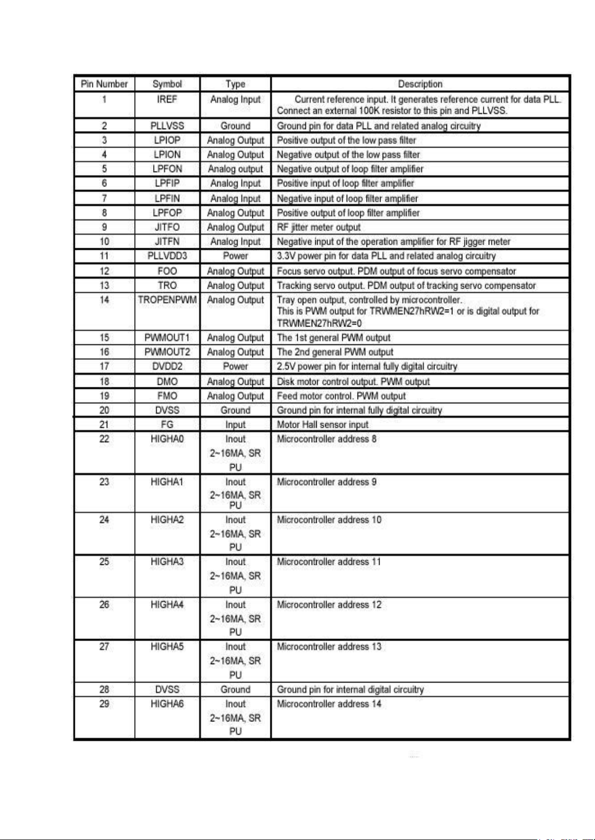
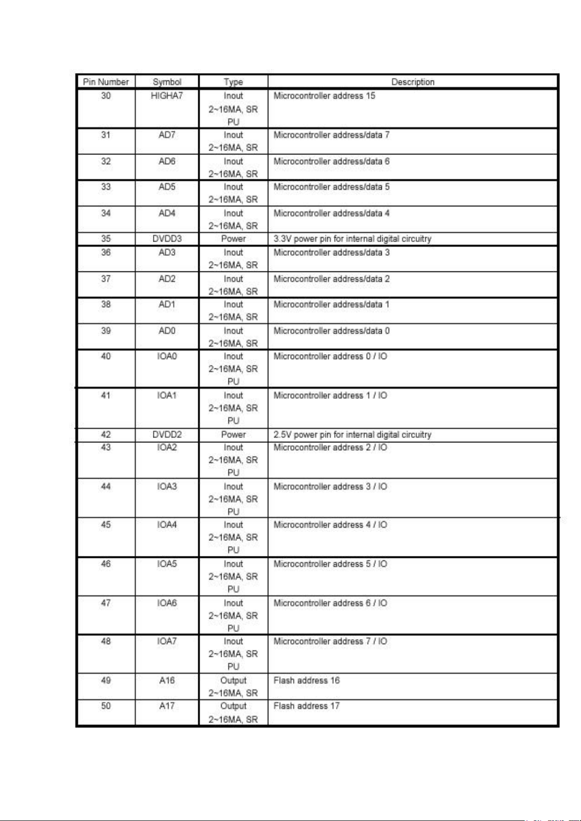
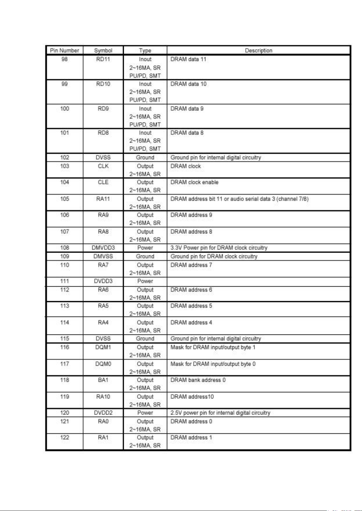
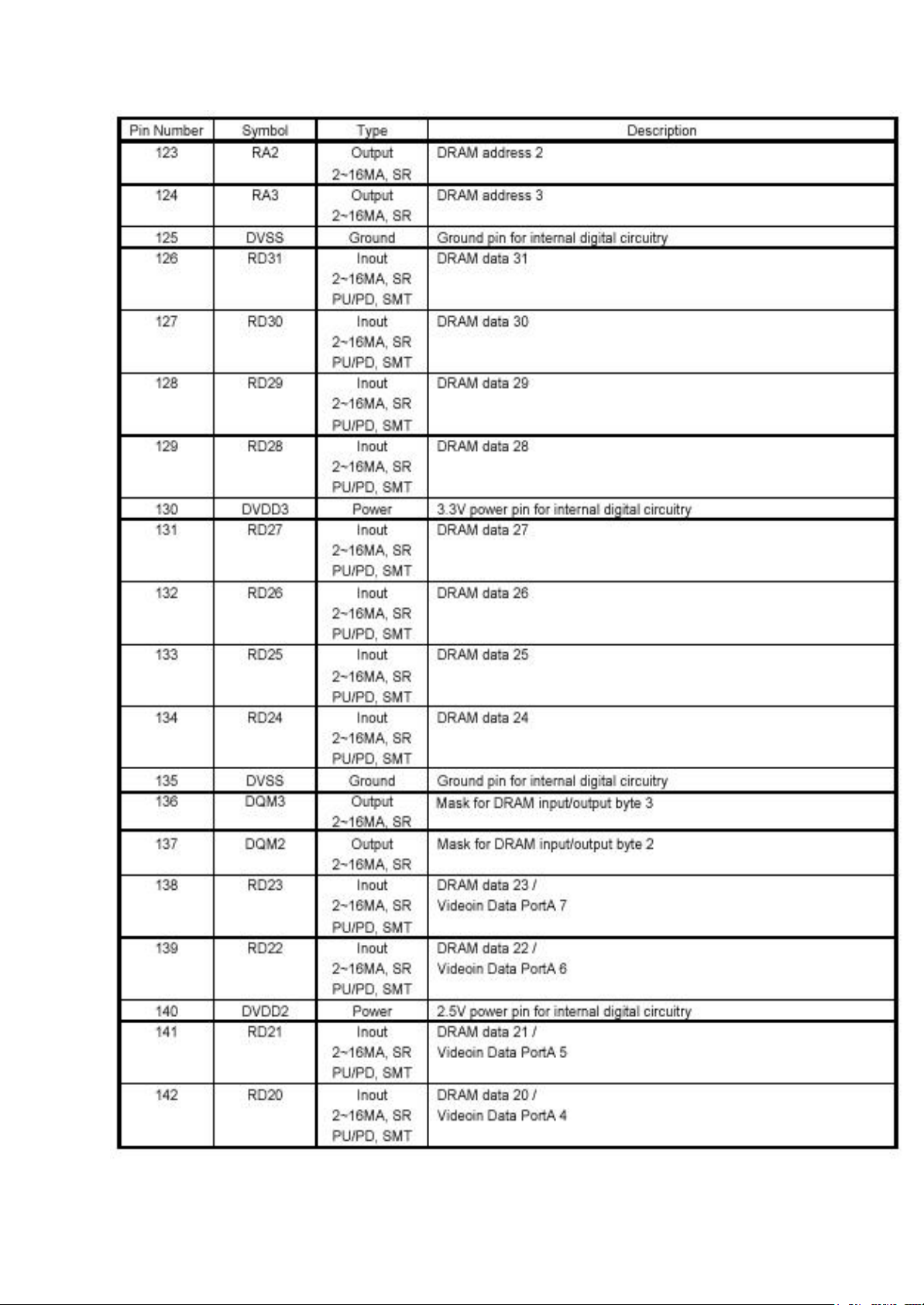
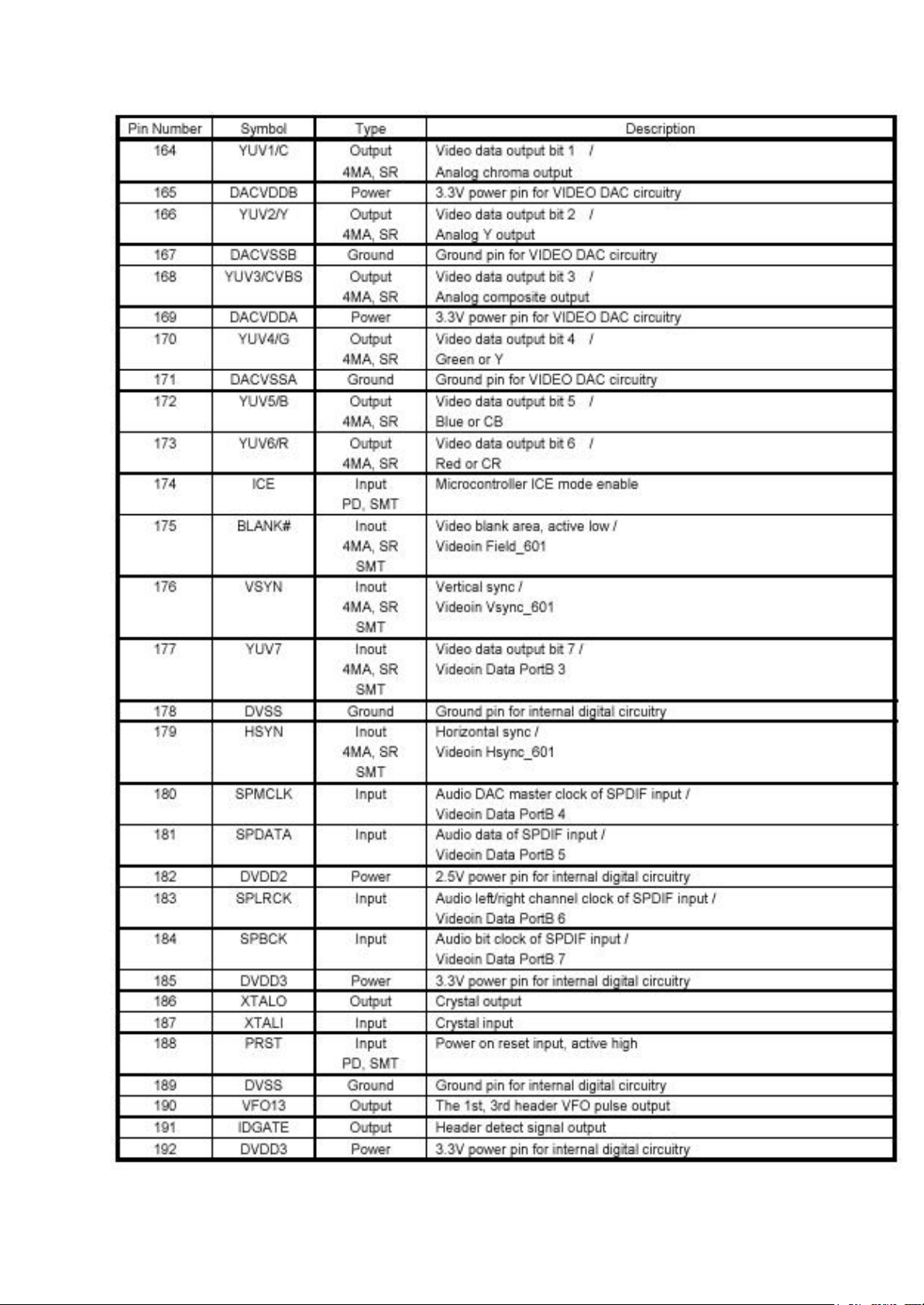
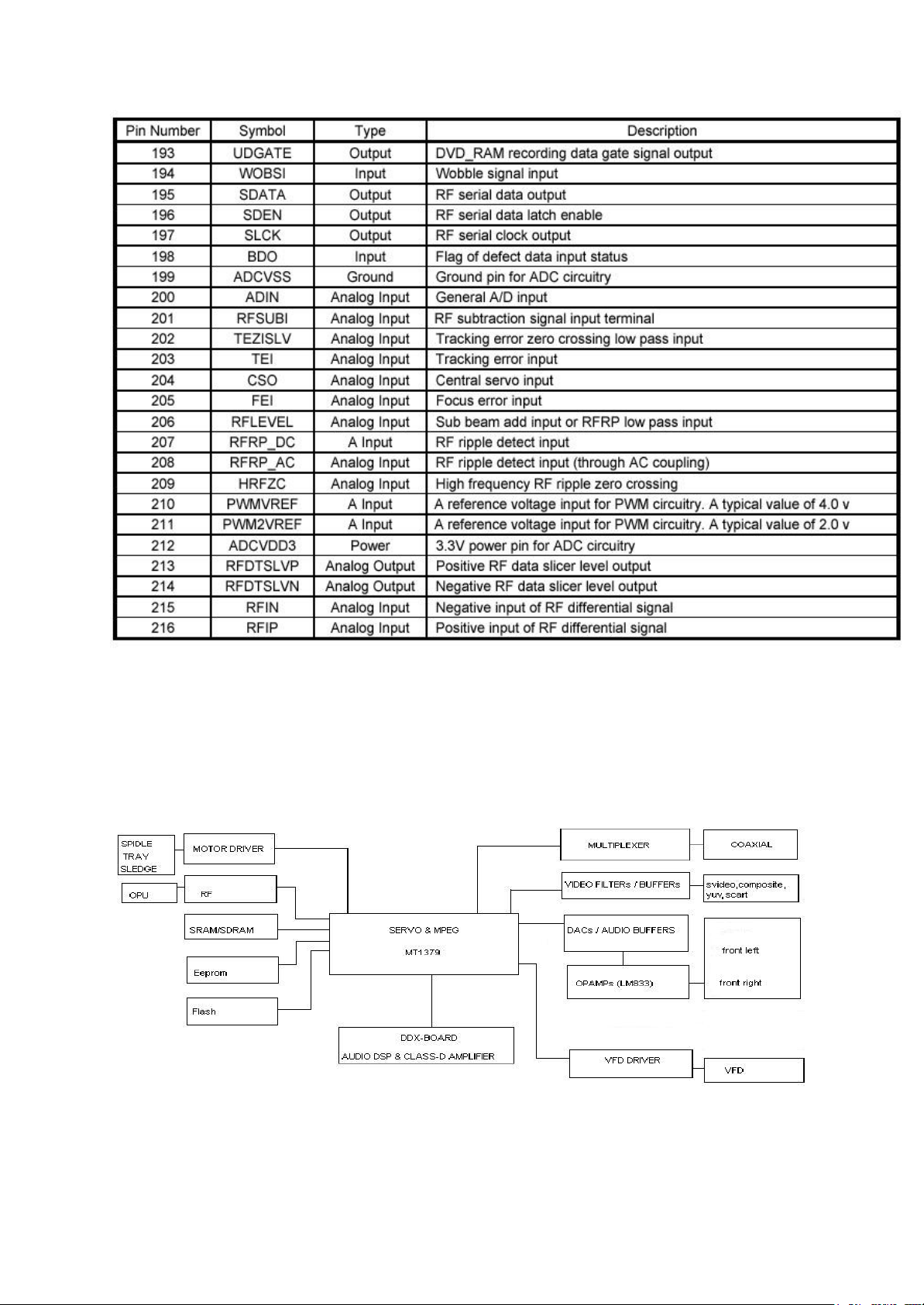
2. SYSTEM BLOCK DIAGRAM and MT1379 PIN DESCRIPTION
2.1 MT1379 PIN DESCRIPTION
Page 5
Page 6
Page 7

Page 8

Page 9
Page 10
Page 11

Page 12
Page 13
2.1 SYSTEM BLOCK DIAGRAM
System block diagram is shown in the following figure:
Page 14

3. AUDIO OUTPUT
The MT1379 supports the stereo (2 channel) outputs .
The MT1379 alTrso provides digital output in S/PDIF format. The board supports coaxial S/PDIF input.
AV2300 has also 5.1 channel Class-D amplifier outputs to 8 ohms satelites and 4 ohms
subwoofer.
4 AUDIO DACS
The MT1379 supports several variations of an I 2 S type bus, varying the order of the data bits (leading or no
leading zero bit, left or right alignment within frame, and MSB or LSB first) is possible usin g the MT1379
internal configuration registers. The I 2 S format uses four stereo data lines and three clock lines. The I 2 S data
and clock lines can be connected directly to one or more audio DAC to generate analog audio output.
The two-channel DAC is an AKM AK4382 . The DACs support up to 192kHz sampling rate.
The outputs of the DACs are differential, not single ended so a buffering circuit is required. The buffer circuits
use National LM833 op-amps to perform the low-pass filtering and the buffering.
5 VIDEO INTERFACE
5.1 Video Display Output
The video output section controls the transfer of video frames stored in memory to the internal TV encoder of the
Vibratto. The output section consists of a programmable CRT controller capable of operating either in Master or
Slave mode.
The video output section features internal line buffers which allow the outgoing luminance and chrominance data
to match the internal clock rates with external pixel clock rates, easily facilitating YUV4: 2:2 to YUV4: 2:0
component and sample conversion. A polyphase filter achieves arbitrary horizontal decimation and interpolation.
Video Bus
The video bus has 8 YUV data pins that transfer luminance and chrominance (YUV) pixels in CCIR601 pixel
format (4:2:2). In this format, there are half as many chrominance (U or V) pixels per line as luminance (Y)
pixels; there are as many chrominance lines as luminance.
Video Post -Processing
The MT1379 video post-processing circuitry provides support for the color conversion, scaling, and filtering
functions through a combination of special hardware and software. Horizontal up-sampling and filtering is done
with a programmable, 7-tap polyphase filter bank for accurate non-integer interpolations. Vertical scaling is
achieved by repeating and dropping lines in accordance with the applicable scaling ratio.
Video Timing
The video bus can be clocked either by double pixel clock and clock qualifier or by a single pixel clock. The
double clock typically is used for TV displays, the single for computer displays.
Page 15

6 FLASH MEMORY
The decoder board supports AMD class Flash memories. Currently 4 configurations are
supported:
FLASH_512K_8b
FLASH_1024K_8b
FLASH_512Kx2_8b
FLASH_512Kx2_16b
The Vibratto permits both 8- and 16 -bit common memory I/O accesses with a removable storage
card via the host interface.
7 SERIAL EEPROM MEMORY
An I2C serial EEPROM is used to store user configuration (i.e. language preferences, speaker setup, etc.) and
software configuration.. Industry standard EEPROM range in size from 1kbit to 256kbit and share the same IC
footprint and pinout. The default device is 2kbit, 256kx 8, SOIC8 SGS Thomson ST24C02M1 or equivalent.
8 AUDIO INTERFACE AUDIO SAMPLING RATE AND PLL COMPONENT
CONFIGURATION
The MT1379 audio mode configuration is selectable, allowing it to interface directly with low-cost audio DACs
and ADCs. The audio port provides a standard I 2 S interface input and output and S/PDIF (IEC958) audio
output. Stereo mode is in I 2 S format while six channels Dolby Digital (5.1 channel) audio output can be
channeled through the S/PDIF. The S/PDIF interface consists of a bi-phase mark encoder, which has low skew.
The transmit I 2 S interface supports the 128, 192, 256, 384, and 512 sampling frequency formats, where
sampling frequency Fs is usually 32 kHz, 44.1 kHz, 48 kHz, 96 kHz, or 192 kHz. The audio samples for the
I 2 S transmit interface can be 16, 18, 20, 24, and 32-bit samples.
For Linear PCM audio stream format, the MT1379 supports 48 kHz and 96 kHz. Dolby Digital audio only
supports 48 kHz. MT1379 incorporates a built -in programmable analog PLL in the device architecture in order
to generate a master audio clock. The MCLK pin is for the audio DAC clock and can either be an output from or
an input to the MT1379. Audio data out (TSD) and audio frame sync (TWS) are clocked out of the MT1379
based on the audio transmit bit clock (TBCK). Audio receive bit clock (RBCK) is used to clock in audio data in
(RSD) and audio receive frame sync (RWS).
9 FRONT PANEL
9.1 VFD CONTROLLER
The VFD controller is a NEC uPD16311. This controller is not a processor, but doesinclude a simple state
machine which scans the VFD and reads the front panel button matrix. The 16311 also includes RAM so it can
store the current state of all the VFD icons and segments. Therefore, the 16311 need only be accessed when the
VFD status changes and when the button status is read. The MT1379 can control this chip by using 3 wire
communication.
10 CONNECTORS
10.1 SCART CONNECTORS
Pinout of the scart connec tor:
1 - Audio Right Out
2 - Audio Right In
3 - Audio Left / Mono Out
4 - Audio Gnd
5 - Blue Gnd
Page 16

6 - Audio Left / Mono In
7 - Blue
8 - Control Voltage
9 - Green Gnd
10 - Comms Data 2
11 - Green
12 - Comms Data 1
13 - Red Gnd
14 - Comms Data Gnd
15 - Red
16 - Fast Blanking
17 - Video Gnd
18 - Fast Blanking Gnd
19 - Composite Video In
20 - Composite Video Out
21 – Shield Gnd
Some cheaper SCART cables use unshielded wires, which is just about acceptable for short cable lengths. For
longer lengths, shielded co-ax cable become essential.
Scart Signals:
Audio signals
0.5V RMS, <1K output impedance, >10K input impedance.
Red, Green, Blue
0.7Vpp ±2dB, 75R input and output impedance. Note that the Red connection (pin 20) can alternatively carry the
S-VHS Chrominance signal, which is 0.3V.
Composite Video / CSync
1Vpp including sync, ±2dB, 75R input and output impedance.Bandwidth = 25Hz to 4.8MHz for normal TV
Video de-emphasis to CCIR 405.1 (625-line TV)
Fast Blanking
75R input and output impedance. This control voltage allows devices to over -ride the composite video input with
RGB inputs, for example when inserting closed caption text. It is called fast because this can be done at the same
speeds as other video signals, which is why it requires the same 75R impedances.
0 to 0.4V: TV is driven by the composite video input signal (pin 19).Left unconnected, it is pulled to 0V by its
75R termination.
1V to 3 V: the TV is driven by the signals Red, Green, Blue and composite sync. The latter is sent to the TV on
pin 19. This signal is useful when using a TV to display the RGB output of devices such as home computers with
TV-compatible frame rates. Tying the signal to 5V via 100R forms a potential divider with the 75R termination,
holding the signal at around 2V. Al ternatively, if a TTL level (0 to 5V) negative sync pulse is available, this will
be high during the display periods, so this can drive the blanking signal via a suitable resistor.
Control Voltage
0 to 2V = TV, Normal.
5 to 8V = TV wide screen
9.5 to 12V = AV mode
Page 17

11. CIRCUIT DESCRIPTION
11.1 POWER SUPPLY:
· Socket PL800 is the 220VAC input.
· 3.5A fuse F800 is used to protect the device against short circuit and unexpected overloads.
· Line filter and capacitors L800, C801 and C803 are used to block the parasitic coming from the mains. They
also prevent the noise, produced in the circuit, from being injected to the line.
· Voltage is rectified by using diodes D805 diode bridge. Using capacitor C815 (100uf) a DC voltage is
produced. (310 - 320VDC).
· The current in the primary side of the transformer TR800 comes to the SMPS IC (IC800 MC44608). The SMPS
IC has a eight-pin DIP-8 package and an external MOSFET with a cooler is mounted on it. It has a built-in
oscillator, overcurrent and overvoltage pr otection circuitry and runs at 100kHz. It starts with the current from the
primary side of the transformer and follows the current from the feedback winding.
· Feedback current is deteceted by optocoupler IC803. Depending on the control current coming from the
secondary side, SMPS IC keeps the output voltage constant by controlling the duty cycle of the ~30kHz signal
(PWM) at the primary side of the transformer.
· Voltages on the secondary side are as follows: +30 Volts at D811, +8 Volts at D808, +15V at D810, -22 Volts at D812,
+12Vst at Q804.
· Using the output of the D808, a photo diode inside of the IC803 generates feedback signal bu using optocoupler's photo
transistor. This photo transistor adjusts the control voltage at the IC800 pin3. The voltage at this pin effects the pwm output
frequency on the IC800 pin5. And finally output voltages reach their correct values by this way.
· Voltage regulator IC805 (LM7805) supplies +5 Volts, IC807 supplies +5V (off on standby mode), IC809 supplies +3.3V
(by using output of the IC807, off on standby mode), Q804 supplies +12Vst, IC806 supplies +12V (off on standby mode),
Q808 supplies -5V, D812 supplies -22V. Standby mode controlled by standby control transistors Q805, Q806, Q807.
· –22 Volts is used to feed the VFD (Vacuum Fluorescent Display) driver IC on the front panel. Using diode R844, –22V is
decreased and connected to the filament winding to produce the DC offset for the filaments.
11.2 FRONT PANEL:
· All the functions on the front panel are controlled by IC300 (MT1379) on the mainboard
· IC300 sends the commands to IC101 uPD16311 via socket PL101 (pins 2,3 and 4).
· There are 16 keys scanning function, 2 LED outputs, 1 Stand-by output and VFD drivers on IC101.
· Pin 52 is the oscillator pin and is connected via R107 56K.
· LED D1 is blue in stand-by mode and off when the device is on.
· Vacuum fluorescent display MD1 is specially designed for AV2300.
· The scanned keys are transmitted via IC101 to IC300 on the mainboard.
· IR re mote control receiver module IC102 (TSOP1836) sends the commands from the remote control directly to
IC300.
· Socket PL102 carries the VFD filament voltage and –22 Volts.
Page 18

11.3 I/Os and Back Panel:
- There are 2 SCART connector , 6 pieces RCA jacks, for audio output, 1 optical digital audio ,1 s-video
output on the back panel.
- TOTX178 is used for laser output.
- For optical audio output S/PDIF is used.
- Q620, Q621 transistors are to mute the audio outputs while switching the state of the unit (power on/of)
- SCART pin 8 controls 16:9 and 4:3 mode .
-
When the pin 8 output of the scart becomes 5 volts, 4:3 mode is selected and 16:9 mode is selected when this is turned off.
-
There are antenna inputs for AM/FM tuner.
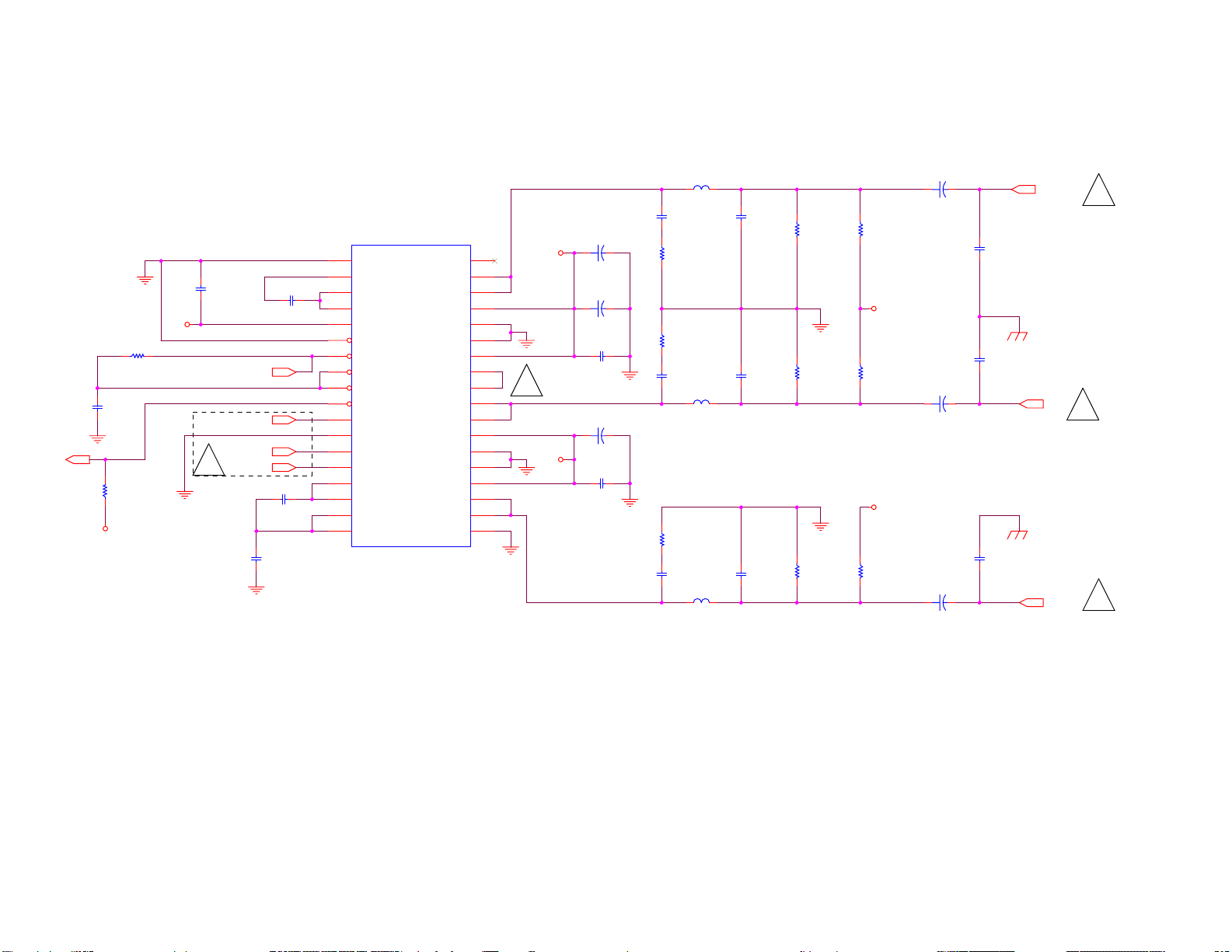
11.4 DDX Board (Class-D Amplifier):
· Chipset : 1xDDX-8228 + 2x DDX-2050
· Architecture : 1xFull-Bridge + 5xHalf -Bridge
· Power Supply : + 30 V unipolar supply @ 6A max., + 3.3V @ 0.1A typ.
· Audio Input Interface: Serial I2S
· Control Interface: I2C
· Power Interface: + 30V @ 6A Max., + 3.3V@ 0.1A Typ
· Output Interface: Speaker Level
· Speakers: 4 Ohm Satellites + 8 Ohm Subwoofer
· Output Power: 5x15 Wrms + 1x25 Wrms
· DDX Audio proccess IC is DDX-8228.
· DDX board have digital audio input with I 2 S bus.
· For mute function, EAPD (pin51, External Amplifier Powerdown) signalis used. This signal comes to the
power output ICs U3 and U4 (DDX-2050 ICs Pin25) as power down signal.
Page 19

12. SOFTWARE
12.1 UNIVERSAL SERVICE PASSWORD
- Universal Password for Parental level is 1369
12.2 VERSION PAGE (Hidden Menu)
To see Version Page:
- Press DISPLAY button from remote for Setup Menu
- Press “1”-“3”-“5”-“7” at Setup Menu
- Setup Menu screen refresh and “Version” selection can be seen under “Preferences Setup”
- Select “Version” for version page
-BUILD NO contains version and Hardware opti on other information for development only.
- Details of Build No as follows:
- Press “DISPLAY” button on remote control to exit menu.
Page 20

12.3 VFD FULL SEGMENT TEST MODE
During Pressing “STOP” button on Front Pannel if you press Standby button all segments of VFD are higligted.
12.4 REGION MANAGEMENT
At Version page by using arrow keys Region can be changed.
12.5 UPDATE FILE NAME
Proper Update file name can be learned from Version Page as follows:
First Characters of DAC, LOADER, TUNER and LANGUAGE group gives proper update file name.
Example: CFK.bin
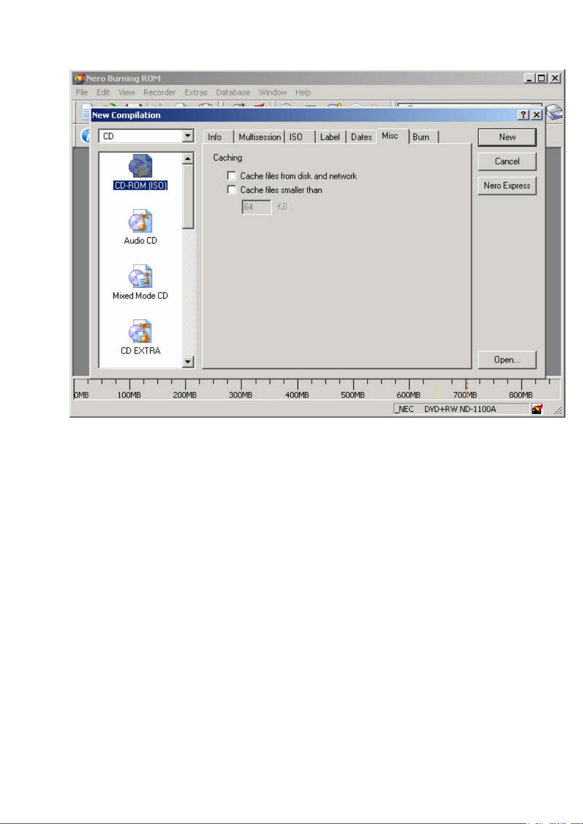
12.5 CD UPDATE PROCEDURE
1) Player can be updated automatically with Update CD which contains proper file.
Check hidden menu for update file name.
2) Burn CD* within proper update file
3) There should be no Volume Name for CD
Open Tray and place update CD
4) You can see
5) Press Play button to start upgrade
6) You can see “File copying” OSD message for a few second
7) Tray is open automatically
8) No need for CD in tray; Take it from away
9) During upgrade procedure “CD upgrade start, Please wait..” indicator at OSD, and “UPG” indicator at VFD
10) Upgrade procedure takes about a few minutes, please wait if tray is open
11) When CD update is finished tray is closed, screen is refreshed, update is finished
NOTE: * For “ NERO Burning Rom” program
Ideal configuration;
Multisession selection should be “No Multisession”
File format should be “ ISO9660” . Do not use “Joliet”
It is better to erase with “Quick Erase” if you use CD-RW before burning
There should be no Volume lable
It may be better to put some dummy files sn CD update file
Page 21

Pay attention the left side. Select CD and CD_ROM (ISO) on the upper left side of screen
Page 22

Select No Multisession
Page 23

Format is Mode 1
Page 24

Page 25

Leave the dates as it is
Page 26
Leave it as it is
Page 27

Click the “New” on the upper right corner of the screen
Select your file from file browser then you will see your file in the “Name” section on the
Page 28

right side and then copy the files to under “Name” section on the left side.(this is just an
example you will see your file name when you are doing this process)
Page 29

Click the “Burns the current compilation”
Then you will see this screen and click the “Burn” on the right upper side of screen
Page 30

Page 31

You will see this screen and tray will open itself on computer ,then place the CD in CD-ROM
And it will start writing. At the end you will see “burn complited”
Page 32

MAIN BOARD
Page 33

Page 34

Page 35

Page 36

Page 37

Page 38

Page 39

Page 40

POWER BOARD
Page 41

FRONT PANEL
Page 42

SDATA0
DDX-BOARD
SDATA1
SDATA2
LRCK
BICK
MCLK
SDA
SCL
PWRDWN
POWER_ON_RST
SDATA0
SDATA1
SDATA2
LRCK
BICK
MCLK
SDA
SCL
PWRDWN
POWER_ON_RST
SDATA0
SDATA1
SDATA2
LRCK
BICK
MCLK
SDA
SCL
PWRDWN
POWER_ON_RST
LEFT_A
CENTER_A
SURRLEFT_A
EAPD
LEFT_A
CENTER_A CENTER+
SURRLEFT_A
EAPD
LEFT_A
CENTER_A
SURRLEFT_A
EAPD TWARN1
Sch_LEFT_SURRLEFT_CENTER_Out
CENTER+
SURRLEFT+
LEFT+
LEFT+
SURRLEFT+
TWARN1
SCH_A_INPUT
TWARN2
TWARN1
TWARN2
TWARN1
Sch_B_Processing
RIGHT_A
SURRRIGHT_A
LFE_A
LFE_B
RIGHT_A
SURRRIGHT_A
LFE_B
RIGHT_A
SURRRIGHT_A
LFE_A
LFE_B
EAPD
Sch_RIGHT_SURRRIGHT_LFE_Out
RIGHT+
SURRRIGHT+
LFE+
LFE-
TWARN2
RIGHT+
SURRRIGHT+
LFE+LFE_A
LFE-
TWARN2
LEFT+
CENTER+
SURRLEFT+
RIGHT+
SURRRIGHT+
LFE+
LFE-
SPEAKER OUTPUT
AMP SCHEMATICS 5X15W+1X25W
Page 43

SDATA0
SDATA2
BICK
+3.3V
R3
NS
0000-0603
R37
R4
NS
0000-0603
TWARN1
R5
NS
0000-0603
SCL
INPUT CONNECTOR
J1
1
3
5
7
9
11
13
15
87256-1611
2
4
6
8
10
12
14
16
0000-0603
NS
R6
SDA
TWARN2
PWRDWN
MCLK
R1
NS
0000-0603
SDATA1
LRCK
R2
NS
0000-0603
+
C7
100NF
Y5V
EIA0603
10K
0000-0603
C1
100UF
10V
100UF-ELEC-16V-RADIAL
C6
+
100UF-ELEC-16V-RADIAL
100UF
10V
+3.3V
C2
100NF
Y5V
EIA0603
+28V
C3
100NF
X7R
EIA0805
U1
LM1117-ADJ
3 2
IN OUT
ADJ
R7
1
R8
154
150 0000-0805
0000-0805
JP1
1
2
3
4
JS-1120-04
+2.5V
C8
+
100UF
10V
100UF-ELEC-16V-RADIAL
C4
100NF
Y5V
EIA0603
POWER_ON_RST
H1
1
DDX2060HS
H2
1
DDX2060HS
POWER_ON_RST
AMP SCHEMATIC INPUT CONNECTOR
Page 44

+2.5V
+3.3V
+3.3V
+2.5V
PWRDWN
+3.3V
C15
100NF
Y5V
EIA0603
C16
100NF
Y5V
EIA0603
+2.5V
0000-0603
LRCK LRCKI
R35
NS
+3.3V
+2.5V
C85
NS
NPO
EIA0603
+3.3V
0000-0603
LRCKI
C21
100NF
Y5V
EIA0603
C26
100NF
Y5V
EIA0603
POWER_ON_RST
(USED ON -01 ONLY)
(USED ON -02 ONLY)
3 4
1
6
5
C86
NS
Y5V
EIA0603
R9
0
R3600000-0603
DQ
CLK
CLR
VCC
GND
2
NC7SZ175/SC70
SDATA2
SDATA1
SDATA0
BICK
U5
NS
C24
1000PF
NPO
EIA0805
C25
NS
NPO
EIA0603
MCLK
SDA
SCL
+3.3V
C10
100NF
Y5V
EIA0603
C14 1000PF
NPO
EIA0805
1
MVO
2
TEST_MODE
3
VDD3.3_1
4
GND_1
5
VDD2.5_1
6
SDI_78
7
SDI_56
8
SDI_34
9
SDI_12
10
LRCKI
11
BICKI
12
VDD3.3_2
13
GND_2
14
VDD2.5_2
15
RESET
PLL_BYPASS
R10
NS
0000-0603
R11
NS
0000-0603
C11
100NF
Y5V
EIA0603
C12
100NF
Y5V
EIA0603
49
LRCKO
CKOUT
26
BICKO
VDD2.5_3
54
VDD2.5_6
GND_3
282027
100PF
NPO
EIA0603
GND_6
VDD3.3_6
VDD3.3_3
OUT8_B
29
C35
50
51
EAPD
OUT1_A
OUT7_B
OUT8_A
OUT1_B
OUT2_A
OUT2_B
VDD2.5_5
GND_5
VDD3.3_5
OUT3_A
OUT3_B
OUT4_A
OUT4_B
OUT5_A
OUT5_B
VDD2.5_4
GND_4
VDD3.3_4
OUT6_A
OUT6_B
OUT7_A
323130
+2.5V
C28
100NF
Y5V
EIA0603
C33
100PF
NPO
EIA0603
GNDA
U2
DDX-8228
C29
100NF
Y5V
EIA0603
60
61
SDO_56
SCL
VDD2.5_7
XTI
GND_7
PLL_FILTER
59
SDO_12
SDO_34
VDD3.3_7
VDDA_PLL
GNDA_PLL
VDD3.3_PLL
221621
23
24
R12
3.40K
0000-0603
C34
1200PF
X7R
EIA0603
56575862555352
25
C27
100NF
Y5V
EIA0603
64
63
PWDN
SDO_78
SDA
SA
181917
C13
100NF
Y5V
EIA0603
EAPD
SURRRIGHT_A
48
47
46
45
44
43
42
41
40
39
38
37
36
35
34
33
VDDA
C31
100NF
Y5V
EIA0603
+3.3V
+
CENTER_A
RIGHT_A
LEFT_A
LFE_A
LFE_B
SURRLEFT_A
C30
22UF
6.3VDC
EIA3528_B
L1
600 ohm@100mhz
1 2
EIA0805
L2
600 ohm@100mhz
1 2
EIA0805
+2.5V
C32
100NF
Y5V
EIA0603
+3.3V
C22
100NF
Y5V
EIA0603
+2.5V
C23
100NF
Y5V
EIA0603
C19
100NF
Y5V
EIA0603
+
+3.3V
C17
2.2UF
6.3VDC
EIA3216_A
C20
100NF
Y5V
EIA0603
+
C18
+2.5V
2.2UF
6.3VDC
EIA3216_A
AMP SCHEMATIC PROCESSING
Page 45
TWARN1
+3.3V
R19 10K
0000-0603
C49
100NF
Y5V
EIA0603
R20
10K
0000-0603
+3.3V
REV3
C41
100NF
X7R
EAPD
SURRLEFT_A
LEFT_A
CENTER_A
C42
100NF
X7R
C52 100NF
X7R
C53
100NF
X7R
20
21
22
23
24
25
26
27
28
29
30
31
32
33
34
35
36
U3
GNDR1
VREG1
VREG1
VL
CONFIG
PWRDN
TRI-STATE
FAULT
TWARN
INLA
INLB
INRA
INRB
VREG2
VREG2
VSIG
VSIG
DDX-2050
OUTPL
OUTPL
VCC1P
PGND1P
PGND1N
VCC1N
OUTNL
OUTNL
OUTPR
OUTPR
VCC2P
PGND2P
PGND2N
VCC2N
OUTNR
OUTNR
GNDS
L3 22uH
1 2
IND-1014P
C37
330PF
1819
NCGNDREF
17
16
15
14
13
12
11
10
9
8
7
6
5
4
3
2
1
+28V
REV3
+28V
C39
+
1000UF
35VDC
C43
+
1UF
35VDC
C45
100NF
X7R
C50
+
1UF
35VDC
C51
100NF
X7R
X7R
R15
20
0000-1206
5%
R16
20
0000-1206
5%
C46
330PF
X7R
L4 22uH
1 2
IND-1014P
R21
20
0000-1206
5%
C55
330PF
X7R
L5 22uH
1 2
IND-1014P
C38
680NF
FILM
C47
680NF
FILM
C56
680NF
FILM
R13
3.3K
0000-1206
5%
R17
3.3K
0000-1206
5%
R22
3.3K
0000-1206
5%
R14
3.3K
0000-1206
5%
+28V
R18
3.3K
0000-1206
5%
+28V
R23
3.3K
0000-1206
5%
C36
+
330UF
35VDC
C48
330UF
35VDC
+
C57
+
330UF
35VDC
C40
1000PF
NPO
C44
1000PF
NPO
C54
1000PF
NPO
SURRLEFT+
4 OHM
4 OHM
LEFT+
4 OHM
CENTER+
REV3
REV3
REV3
AMP SCHEMATIC LEFT, SURRLEFT CHANNELS AMPLIFIER
Page 46

TWARN2
+3.3V
+3.3V
C72
100NF
Y5V
EIA0603
R31
10K
0000-0603
C62
100NF
X7R
R27 10K
0000-0603
SURRRIGHT_A
EAPD
LFE_A
LFE_B
RIGHT_A
C79 100NF
C80
100NF
X7R
X7R
C65
100NF
X7R
20
21
22
23
24
25
26
27
28
29
30
31
32
33
34
35
36
U4
GNDR1
VREG1
VREG1
VL
CONFIG
PWRDN
TRI-STATE
FAULT
TWARN
INLA
INLB
INRA
INRB
VREG2
VREG2
VSIG
VSIG
DDX-2050
OUTPL
OUTPL
VCC1P
PGND1P
PGND1N
VCC1N
OUTNL
OUTNL
OUTPR
OUTPR
VCC2P
PGND2P
PGND2N
VCC2N
OUTNR
OUTNR
GNDS
L6 22uH
1 2
IND-1014P
1819
NCGNDREF
17
16
15
14
13
12
11
10
9
8
7
6
5
4
3
2
1
+28V
+28V
C59
+
1000UF
35VDC
C66
+
1UF
35VDC
C70
100NF
X7R
C74
+
1UF
35VDC
C77
100NF
X7R
R24
20
0000-1210
5%
C67
330PF
X7R
L7 22uH
1 2
IND-1014P
L8 22uH
1 2
IND-1014P
C75
330PF
X7R
R30
20
0000-1206
5%
L9 22uH
1 2
IND-1014P
C82
330PF
X7R
R34
20
0000-1206
5%
C58
100NF
X7R
R25
6.2
0000-1206
5%
R26
6.2
0000-1206
5%
C71
100NF
X7R
C76
680NF
FILM
C83
680NF
FILM
C61
100NF
X7R
C68
100NF
X7R
R28
3.3K
0000-1206
5%
R32
3.3K
0000-1206
5%
C63
470NF
FILM
R29
3.3K
0000-1206
5%
+28V
R33
3.3K
0000-1206
5%
+28V
C60
1000PF
NPO
C69
1000PF
NPO
C73
+
330UF
35VDC
C81
+
330UF
35VDC
C64
1000PF
NPO
C78
1000PF
NPO
C84
1000PF
NPO
LFE+
LFE-
RIGHT+
4 OHM
SURRRIGHT+
4 OHM
8 OHM
AMP SCHEMATIC CENTER, LFE CHANNEL AMPLIFIERS
Page 47

SRIGHT
- OUT
+ OUT
LFE-
12
J2
PT1201
..
34
..
56
..
78
..
910
..
1112
..
SURRRIGHT+
RIGHT+
LFE+
CENTER+
LEFT+
SURRLEFT+
SPEAKER
AMP SCHEMATIC OUTPUT CONNECTOR
RIGHT
LFE
CENTER
LEFT
SLEFT
Rear Panel View
Page 48

THE UPDATED PARTS LIST
FOR THIS MODEL IS
AVAILABLE ON ESTA
Page 49

Hitachi, Ltd. Tokyo, Japan
International Sales Division
THE HITACHI ATAGO BUILDING,
No. 15 –12 Nishi Shinbashi, 2 – Chome,
Minato – Ku, Tokyo 105-8430, Japan.
Tel: 03 35022111
HITACHI EUROPE LTD,
Whitebrook Park
Lower Cookham Road
Maidenhead
Berkshire
SL6 8YA
UNITED KINGDOM
Tel: 01628 643000
Fax: 01628 643400
Email: consumer-service@hitachi-eu.com
HITACHI EUROPE GmbH
Munich Office
Dornacher Strasse 3
D-85622 Feldkirchen bei München
GERMANY
Tel: +49-89-991 80-0
Fax: +49- 89-991 80-224
Hotline: +49-180-551 25 51 (12ct/min)
Email: HSE-DUS.service@hitachi-eu.com
HITACHI EUROPE srl
Via Tommaso Gulli N.39, 20147
Milano, Italia
ITALY
Tel: +39 02 487861
Tel: +39 02 38073415 Servizio Clienti
Fax: +39 02 48786381/2
Email: customerservice.italy@hitachi-eu.com
HITACHI EUROPE S.A.S
Lyon Office
B.P. 45, 69671 BRON CEDEX
FRANCE
Tel: +33 04 72 14 29 70
Fax: +33 04 72 14 29 99
Email: france.consommateur@hitachi-eu.com
HITACH EUROPE AB
Egebækgård
Egebækvej 98
DK-2850 Nærum
DENMARK
Tel: +45 43 43 6050
Fax: +45 43 60 51
Email: csgnor@hitachi-eu.com
Hitachi Europe Ltd
Bergensesteenweg 421
1600 Sint- Pieters-Leeuw
BELGIUM
Tel: +32 2 363 99 01
Fax: +32 2 363 99 00
Email: sofie.van.bom@hitachi-eu.com
www.hitachidigitalmedia.com
HITACHI EUROPE S.A.
364 Kifissias Ave. & 1, Delfon Str.
152 33 Chalandri
Athens
GREECE
Tel: 1-6837200
Fax: 1-6835964
Email: service.hellas@hitachi-eu.com
HITACHI EUROPE S.A.
Gran Via Carlos III, 86, planta 5
Edificios Trade - Torre Este
08028 Barcelona
SPAIN
Tel: +34 93 409 2550
Fax: +34 93 491 3513
Email: atencion.cliente@hitachi-eu.com
HITACHI Europe AB
Box 77 S-164 94 Kista
SWEDEN
Tel: +46 (0) 8 562 711 00
Fax: +46 (0) 8 562 711 13
Email: csgswe@hitachi-eu.com
HITACHI EUROPE LTD (Norway) AB
STRANDVEIEN 18
1366 Lysaker
NORWAY
Tel: 67 5190 30
Fax: 67 5190 32
Email: csgnor@hitachi-eu.com
HITACHI EUROPE AB
Neopoli / Niemenkatu 73
FIN-15140 Lahti
FINLAND
Tel : +358 3 8858 271
Fax: +358 3 8858 272
Email: csgnor@hitachi-eu.com
HITACHI EUROPE LTD
Na Sychrove 975/8
101 27 Praha 10 – Bohdalec
CZECH REPUBLIC
Tel: +420 267 212 383
Fax: +420 267 212 385
Email: csgnor@hitachi-eu.com
 Loading...