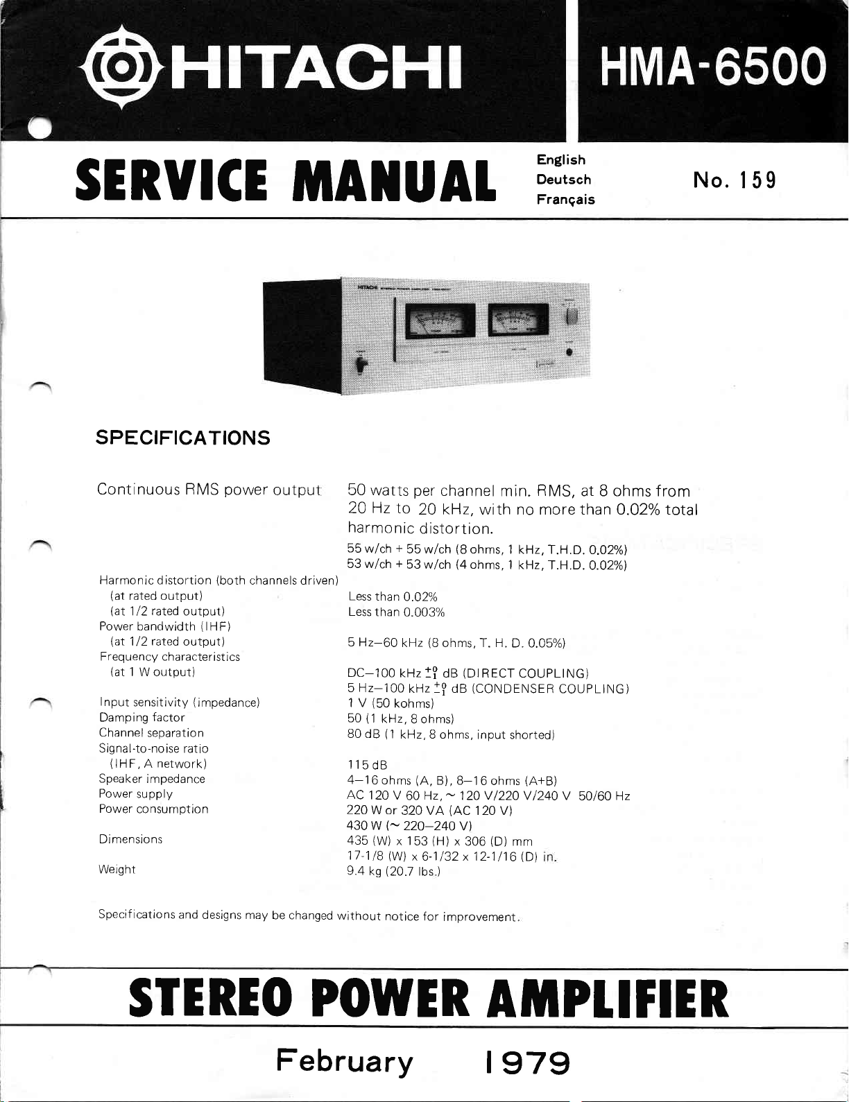
Hitachi HMA-6500 Service manual
SERUICE
SPECIFICATIONS
MATUA1
English
Deutsch
Franqais
No.
159
Continuous RMS
output)
(lHF)
output)
j
(
mpedance)
ratio
(both
Harmonic d istortion
(at
rated output)
rated
1
12
lat
Power bandwidth
(at
rated
1
l2
Frequency characteristics
(at
1 W output)
I
nput
sensitivity
(lHF,
A
supply
consumpllon
factor
separation
network)
impedance
Damping
Channel
Slgnal-to-noise
Speaker
Power
Power
Dimensio ns
Weight
power
outpul
channels driven)
50
watts
20 Hz Io
harmonic
w/ch
than
than
(SO
(1
kHz,
dB
ohms
120
(W)
kg
kohms)
(1
V
or
(-
(wl
(20.7
+
+
kHz
KHZ
kHz, 8 ohms,
320 VA
x 153
55
53 w/ch
Less
Less
5 Hz-60
DC-1OO
5Nz-100
1 V
50
80 dB
115
4-16
AC
22OW
430 W
435
11-118
9.4
per
channel
min.
RMS,
at 8 ohms from
20 kHz, with no more than 0.02% total
distortion.
(8
ohms, T. H.
1? dB
(A,
B), 8-16
-
(H)
lbs
)
(8
ohms,
(4
ohms,
(DIRECT
(CONDENSER
input shorted)
ohms
v
120
x
120 V)
306
l22O
(D)
(AC
1 kHz, T.H.D
1
kHz, T.H.D
D. 0.05%)
COUPLING)
COUpLtNG)
(A+B)
V
v
1240
mm
Dl
O.O2%l
.
.0.02%l
50/60 Hz
55 w/ch
53 w/ch
0.02%
0.003%
kHz 1? dB
8 ohms)
60 Hz,
220-240V1
x 6-1132 x 12-1116
Specif ications
and
designs may
STEREO
be changed
wlthout
notice
POWER
Febru
ary
for
improvement
AIhPI.ITIER
I
979
t
Sinusdauerleistung
Klirrfaktor
(bei
(óei
Leistungsbandbreite
(bei
Frequenzgang
Eingangsempf
(
I mpedanz)
Dampf
Kana
Geràu
(lHF,
Lautsprecherim
Netzspan
Leistu ngsauf
Abmessu ngen
Gewicht
Anderungen der
(beide
Nennlelstung)
1
NennleistÙng)
12
112 Nennleistung)
(bei
lich
ind
aktor
u ngsf
ltrennung
nu
ngsabsta
pedanz
ng
nahme
technischen
schspannu
A-Netz)
(
MS)
R
Kanàle
(
I HF)
1
Watt)
keit
betrieben)
nd
Daten
bleiben
SOWKanal
Gesamtkl irrfaktor
55 W/Kanal
WlKanal
53
Wen iger als O
Weniger als 0,003%
Hz
5
Gleichstrom-l00
5 Hz
1 V
50
{1
80 dB
*'SOWlKanal
+
+
,02o/o
kHz
60
-
100 kHz l?
-
(50
kOhm)
kHz, 8 Ohm)
(1
kHz,8
0,02%)
W/Kanal
55
53
W/Kanal
(8
Ohm, Gesamtklirrfaktor 0,05%)
kHz 1Î Oa
d
Ohm,
1l5dB
(-220
x 153
(A,
120
320
-
VA
240
(H)
B),
V
x
4
16Ohm
-
Wechselstrom
22OW oder
430W
(B)
435
ks
9,4
im Sinne der stàndigen
(g
(
Kapazitive
B
Eingang
16Ohm
8
-
Ohrn;20
(8
Ohm,.1
(+
Ohm,"'!.
(Oiret<tkopplung)
Hz
-20
Gesamtklirrfaktor
kHz,
kHz, Gesamtktirrfaktor
Kopplung)
kurzgeschlossen)
(A+
B)
60H2,-12OVl22OVl24O
20 V Wechselstrom)
f
Vl
(T)
306
mm
Verbesserung
vorbehalten.
kHz,
V 50i60
O
O,O2%l
Hz
'O2%l
SPECIFICATIONS
Pu
issance
effective continue
puissance
la
puissance
f
de
réq
sortie 1
(
impedance)
/bru
A)
(avec
uence
W)
it
Distorsion
(à
(à
harmonique
puissance
la moitié
sortie nominale)
passante
Bande
(à
la moitié de la
nominale)
sortie
Caractéristiques
(à
puissance
Sensibi lité
Coeff icient
Séparation
Rapport
(lH
lmpédance
d'entrée
d'a
de canal
signal
F, Réseau
d'enceinte
Alimentation
Consommation
Dimensions
Poids
de sortie nominale)
de
(lHF)
de
mortissement
sígnal
d'énergie
les deux
de
de
canaux)
50
w/ch
55 w/ch
53 w/ch
lnférieure
lnf
érieure
5 Hz
-
CC_lOO
Hz-100
5
(50
V
1
(1
50
kHz,8
(1
80
dB
115d8
4-1
6 ohms
CA
1
20
22OW
ou
(-220-24OVl
430W
(L)
435
9,4 ks
+
50 w/ch
+
55 w/ch
+
53 w/ch
à
0,02%
à
0,003%
60 kHz
KHZ
kHz
kohms)
ohms)
kHz,8
(A,B),
V
6O
320 VA
'153
x
(8
ohms,
(8
ohms, 1 kHz, D.H.T.
(4
ohms,
(8
ohms, D.H.T.
(COUPLAGE-DIRECT)
dB
1?
(coupLAGE
l? dB
ohms, entrée
8-16 ohms
Hz,
12O V
3OO
1220
120 V)
(P)
(H)
-
(CA
x
Nz
20
1 kHz,
0,05%)
court
(A+B)
V
mm
20 k1z,
-
D.H.T.
pAR
circuitée)
l24O
H.T.
D.
O,O2%"1
O,02"/"1
O,O2y"l
CONDENSATEUR)
v
50/60 Hz
ît
l
I
i
I
I
Les caractéristiques
techniques
présentation
et
a
peuvent
étre
.,
modif iées
sans
préavis
en
raison
d'améliorations.
l
l
l
I
i
I
I
DISASSEMBLY
DEMONTAGE
^
o
Removing the
.
Ausbau
o
Déposer
cover,
Abdeckung, der Schildanbringung
der
le
supérieur,
AND REPLACEMENT.
ET
escutcheon
le cache-entrée
REMONTAGE
ass'y
ZERLEGUNG
The numbers
respond
ZifÍern
Die
entsprechen denen
numéros encerclés
Les
ceux de
à
in the
to those
in the
den Kreismarkierungen
in
in der
la liste de
I
@
I
pièces
,sPxeor@l
UND
circle marks
replacement
Ersatzteilliste.
le
sur
de remplacement,
AUSTAUSCH.
in the diagram cor-
parts
list.
Diagramms
des
schéma
correspondent
2
o
Removing the
o
Ausbau der
o
Déposer
POWER
Leisîun
Tronsisîor
POWER MOS
Leistungs - MOS
le
transistor
MOS
FET(x4)
gs-MOS
3Éx16
ò
-FET(x
effet
(xB)
FET
à effet de
de
chomp(x4)
-
champ
4
)
FET
fo
.3cx6or
(xz)
@
Fig. I
Abb.
Fig.2
Abb.2
I
3Éx8DT(x.,@ì
-3-
HITACHI HMA.6500
o
Removing the
printed
Powen
boards
wiring
supply
o
(A
Stromqúíb
Alimentoîion
Ausbau
der Leitterplatten
3q6Dr
úeor
t
3 I
O
o
^
(O
frloin
omp
Houptversîórker
Amplif
icoteur
5q
Déposer
@
'Woshcr
_kl) @
plaquettes
des
principo
à circuit imprimé
I
I
î.
SERVICE
o
As this unit uses a
careful
repairing.
(1)
To check
to cut off the
Discharge
a resistor
positions
When
discharging through the chassis
danger that
mixed, in this
the
(2)
.
.
@
not
Do
voltmeter
current as malfunction may
meter carefully.
driver.
Parts installation method
Great
care
safety of
tubes,
or they are
board surface. Be sure
tions after
DIRECT
this is
Since
in equipment
occurs
amplified
deterioration
POINTS
the following
of
repair
and
power
power
the
approx.
of
C803
and C804.
Rl or R2 may
case, so be
andQ terminals
touch the terminals
when connecting it for
is
taken
products.
replacing
COUPLING/CONDENSER
a DC amplifier,
and
a DC bias
tone
of
large capacity
points
printed
the
pull
and
capacitors by
10 ohms, 5 watts
be
sure
the electrolytic capacitor.
of
of
result. Handle the DC volt-
Wind insulating tape around the screw-
installing
in
example,
For
kept away from the
maintain
to
parts
for repair.
when
connected
placed
is
quality
and
power
supply,
checking
when
boards,
wiring
out the
power
touching it
capacity at the
ground,
open and noise becomes
bé sure
cord.
there is
to discharge between
nearby
parts
with a DC
adjusting the idle
parts
to improve
parts
are covered
printed
previous
the
COUPLING
direct current
to the input, it
the
to
speaker
generation
of distor-
wiring
condi
switch
leakage
will be
causing
be
and
with
the
with
Fig. 3
Abb.3
tion : this switch
This al.so
because
damage
noise
change
of trouble in the control amplifier
the speaker. If there
("puu
to
prevents
prevents
is heard when turning
...")
CONDENSER COUPLING at that time.
this.
the flow of a large DC component
which would
if
leakage in the input,
DC
switch, so
this
oRl
ground
The
the unit are connected
in Fig. 4.
c
is
The
case, and in order to
and the radiation fan, stability deteriorates by this, so
the FET is isolated
47
ohms.
Accordingly, be careful
ing
the
charge the
this may
nolse.
of
round
orR
because the
lead
Q
electrolytic
cut
the
the signal
lr.
wire of
lead wire of
line and
using Rl
POWER MOS FET is
maintain the capacity between FET
from
the chassis
not to cause an
the speaker to the
capacitor during servicing,
the
(47
v>
ground
Chassis
using
or R2 and introduce
Rl
ground
chassis
ohms) as shown
in the source
a resistor
by
output
chassis or dis-
Fig.4
touch-
since
of
of
î
a
î
-4-
HITACHI HMA-6500
.
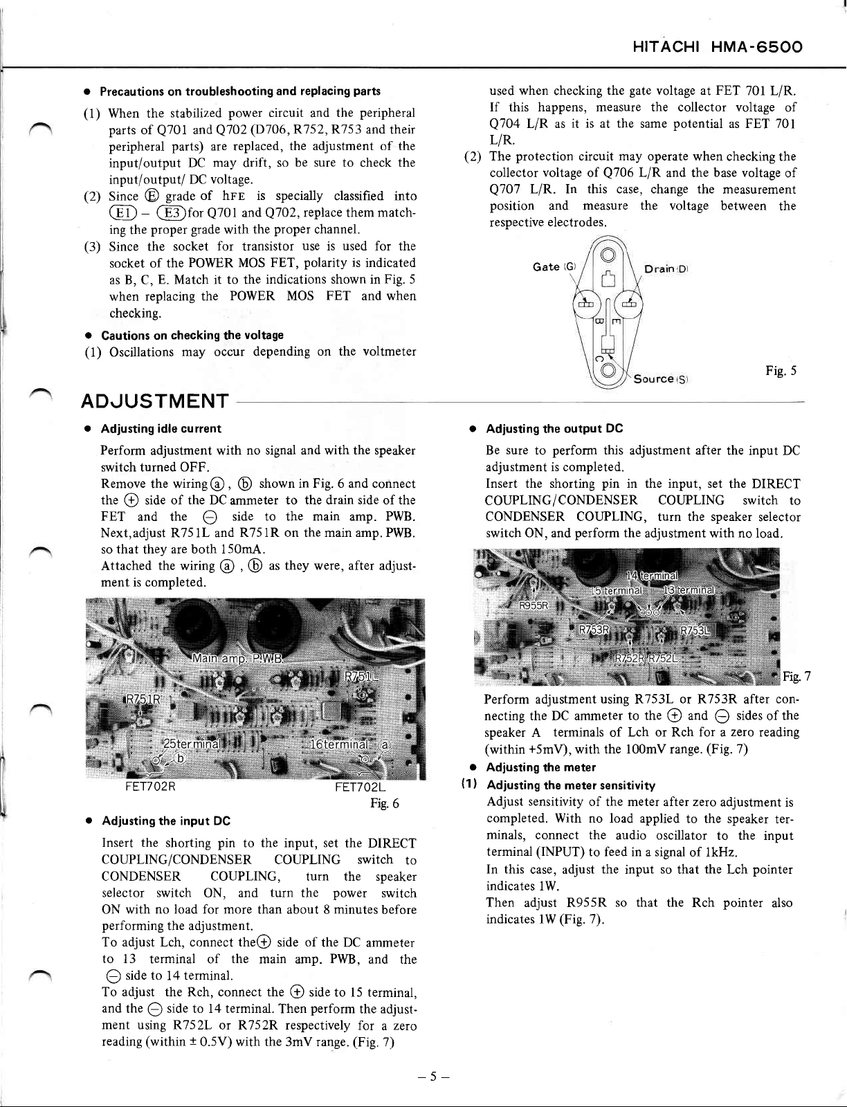
Precautions on
(1)
When
parts
of
peripheral
input/output DC
input/output/
(2)
Since
@
-
ing
the
(3)
Since
socket of the
as B, C,
when replacing
checking.
.
Gautions
(1)
Oscillations
troubleshooting
stabilized
the
and
Q701
parts)
are replaced,
may
voltage.
DC
grade of hrs is specially
@
@fo.
proper grade
the
E. Match it to the
Q701
socket
POWER MOS FET,
the
checking
on
may occur depending
ADJUSTMENT
.
Adjusting idle current
Perform
switch turned OFF.
Remove the wiring
the
FET
Next,adjust R75 lL and
so that
Attached
ment is completed.
adjustment with
of the DC
side
@
and the
are both 150mA.
they
the
wiring
@
O
parts
the
peripheral
power
Q702
and replacing
circuit
(D106,
and
R752, R753 and
the adjustment of the
so be sure to check the
drift,
classified into
and
the
with
for
transistor
POWER MOS
voltage
the
replace
Q702,
proper
use
polarity
indications shown in
them
channel.
used
is
FET
is
indicated
and when
on the voltmeter
no signal and with the speaker
shown in Fig. 6 and connect
,
@
ammeter
to the drain side of the
side to the main amp. PWB.
R75 lR on the main amp. PWB.
as they were, after adjust-
,
@
@
their
match-
for the
Fig.
used
when checking
If this happens, measure the collector voltage
LiR as
Q704
L/R.
(2)
protection
The
collector
Q707
position
respective
5
o
Adjusting
sure
Be
adjustment is completed.
Insert the shorting
COUPLING/CONDENSER
CONDENSER COUPLING, turn the speaker
switch ON, and
it is at the
circuit may operate when
voltage
L/R. In this case, change the
Gate
the
to
of
measure the
and
electrodes.
(G)
output
perform
perform
gate
the
Q706
voltage at FET
potential
same
L/R
and the
voltage between
DC
this adjustment after
pin
in the input, set
COUPLING
the
adjustment with no load.
701 L/R.
as FET 701
checking the
base
voltage
measurement
the input
the DIRECT
switch to
selector
of
of
the
Fig. 5
DC
IEI|OZR
FETT02R
o
Adjusting the input DC
Insert the
shorting
pin
COUPLING/CONDENSER
to the input, set
COUPLING
FETTOZL
Fig.6
Fig.
the DIRECT
switch
CONDENSER COUPLING, turn the speaker
selector switch
ON with
performing
no load for more
the adjustment.
ON,
turn
and
than about 8
To adjust Lch, connect the@
to 13
Q
To adjust the Rch, connect the
and
terminal of
side to
14
the
side to 14 terminal.
Q
terminal.
ment using R152L
reading
(within
the
main amp.
or R752R respectively
t
0.5V) with the 3mV range.
side
@
Then
powet
the
minutes
of
the DC
side to l5 terminal,
perform
PWB,
arnmeter
and the
the adjust-
for
(Fig.
6
switch
before
zero
a
7)
Fig.7
Perform adjustment
necting the DC ammeter
speaker A
(within
o
Adjusting
(1)
Adjusting
Adjust sensitivity
completed.
terminals
+5mV),
the
the meter sensitivity
With no load applied
minals, connect the
to
terminal
In this
indicates
Then
indicates lW
(INPUT)
case, adjust
1W.
adjust R955R
using
R753L
to the
Lch or Rch for a
of
the l00mV range.
with
meter
of the meter after zero
audio oscillator
to feed in a signal
the
input
so that
(Fig.
7).
or
R753R after
and
@
(Fig.
to the speaker
of lkHz.
so
that
the
the Rch
sides
zero
7)
of
reading
ter-
Q
adjustment
to the input
pointer
Lch
pointer
also
con-
the
is
-5-
HITACHI
HMA.6500
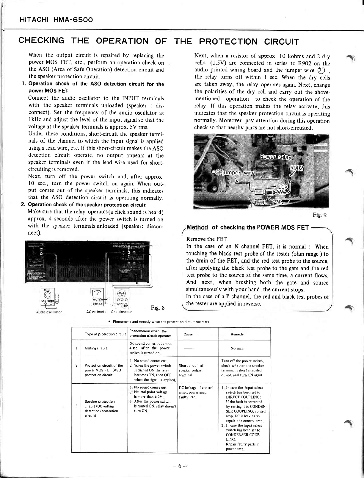
CHECKING
When
the
output circuit is
power
MOS
FET, etc.,
the
the
1. Operation
power
Connect the
with
connect).
lkHz
voltage
Under these
nals of
using a
detection circuit
speaker
circuiting
Next,
10
put
that
2. Operation check
Make
approx. 4 seconds
with
nect).
(Area
ASO
speaker
protection
check
MOS FET
audio
speaker
the
the frequency
Set
and adjust
at the speaker
conditions,
the channel
lead wire, etc.
terminals
is removed.
turn off the
sec., turn the
comes
out
the ASO
sure
that the relay
the
speaker
THE
of
Safe Operation)
OPERATION
repaired
perform
by replacing
an
operation
detection
circuit.
of
the ASO
oscillator
detection circuit
to the INPUT
terminals unloaded (speaker
of the audio
the level
operate, no
even
of the speaker
detection
of
terminals
of the input
terminals
short-circuit
to which the
If this
short-circuit makes
if
lead wire
the
power
power
switch and,
switch
circuit
the
after
speaker
protection
operates(a
power
the
unloaded
ACvolîmeler 0scilloscope
protection
TVpe
of
l Muting circuil
Protection
2
3
power
l\4OS FET
protection
Speaker
(DC
circuit
detection
circuit)
circuit
circuit)
protection
voltage
protection
/
signal so
is approx. 5V
the
input
output
on again.
terminals,
is operating normally.
click
switch
(speaker:
o
Phenomena and remedy
circuil
the
of
(ASO
OF
the
check
circuit
and
for
the
terminals
:
dis-
oscillator
that
the
rms.
speaker
signal is applied
appears
used
after
circuit
sound is
Phenomenon
protecîion
No sound comes
4 rec. after the
switch is turned
I No sound
2. When the
termi-
the
ASO
at the
for short-
approx.
When
out-
this indicates
heard)
is turned
is turned
becomes
when the
No
sound comes out.
Neutral
is more
After the
is tumed
tum ON
on
discon-
Fig.
when the
when
circuit
out about
on
comes out
power
ON the relay
ON, then
signal is
point
voltage
i
thil
2V
power
ON, rclay doesn't
on
at
8
the
operates
power
switch
OFF
applied
switch
THE
proîection
Cause
Short circuiî of
speaker output
teminal
DC leakage of control
amp
faulty,
PROTECTION
Next,
when a resistor
(1.5V)
cells
printed
audio
the
relay
turns off
are
taken
away,
polarities
the
mentioned
relay.
indicates
normally.
check
Remove the FET.
In the case
touching the black
the
drain of the FET,
after
applying the
test probe
And next,
simultaneously
In
the case of a P
the tester
circuit operates
power
amp.
,
etc
operation
If
this operation
that
Moreover,
so that nearby
of checking
of an N channel
to the source
when brushing
with
are applied
Turn
check whether
teminal is
or
not, and tum ON again.
I ln care
switch has been set to
DIRECT COUPLING:
If the fault is corrected
by setting it to coNDEN-
SER COUPLING, control
amp. DC is leaking so
repair the control
2 In case the input s€lect
vitch
CONDENSER COUP.
LINC:
Repair faulty
power
of
approx.
are connected
wiring board
within I
the relay
of the
dry cell
to check
makes
the speaker
test probe
black test
your
channel, the
in reverse.
Remedy
Normal
the
off
short
the
has
amp
protection
pay
attention
parts
are not short-circuited.
POWER
the
of the tester
and the red test
probe
at the same
hand,
power
switch,
the
speaker
circuited
input select
mp
been set to
parts
in
CIRCUIT
l0
kohms
in series
and the
operates
FET, it is normal :
both
the current
red and black test probes
jumper
sec.
When
again.
and
carry
the
the relay
circuit
during
MOS
probe
to
the
time, a current
gate
the
and2
to R902
wire
the
dry cells
Next,
out
the above-
operation
activate,
is operating
this
operation
FET
(ohm
range
the
to
gate
and
and source
stops.
source,
the red
dry
on
the
@
change
of
the
this
When
to
)
flows.
of
î
,
î
î
^
î
-6-
HITACH]
HMA.6500
^
,^
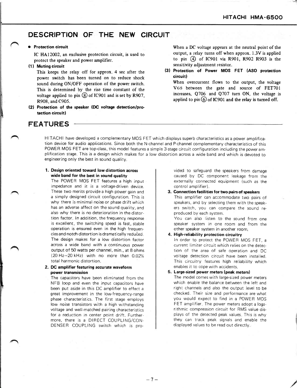
DESCRIPTION
o
Protection circuit
exclusive
an
(1)
IC
HA12002,
protect
Muting
the speaker and
circuit
This keeps the relay
power
sound during
This
voltage applied to
R908, and
(2)
Protection
tection
switch has
is determined
circuit)
C905.
of
been turned on to reduce shock
ON/OFF
by
pin
speaker
the
FEATURES
HITACHI have
tion
device
POWER MOS
plification
engineering only
1.
Design
wide band
POWER N/OS
The
impedance and
These two merits
simply
a
there
why
has an adverse affect on the
also
why
tion factor. ln
excellent,
is
operation is ensured even in
ciesand notch
The design
across a wide band
output of 50 watts
(2O
Hz-2O kHz)
total
2.
amplifier featuring
DC
power
capacitors
The
NFB
been
great
phase
low
noise transistors
voltage
for
a
more, there
DENSER
developed
for
audio applications.
FET are top-class, thls
stage. This is a
the
oriented
for the
designed circuit configuration.
is minimai noise
there
the switching
makes
harmonic
transmission
and even
loop
put
aside in this
improvement in the low-frequency-range
characteristics.
and well-matched
reduction in center
is a DIRECT
COUPLTNG switch
OF
power
off
operation
@
toward low
is
addition, the
distortion is dramatically
THE
protection
amplifier.
for
approx.
rise
the
best
best
it
provide
no
time
IC90l
of
(DC
voltage
a complementary
design which
in sound
in
sound
FET features
is
voltage-driven
a
a high
deterioration
for
a low
NEW
circuit,
4 sec
power
of the
constant
and is set by R907,
detection/pro-
Since
model features
quality.
distoftion
quality
a high
power
phase
or
frequencv
speed is fast,
drift
quality,
sound
in the
the high frequen-
distortion
with a continuous
per
channel,
with no
distortion.
accurate waveform
have
been
min.,
more than
eliminated
the input capacitors
DC amplifier to
first
The
with a high
stage
withstanding
pairing
characteristics
point
drlft. Further-
COUPLING/CON
which
CIRCUIT
When a DC voltage appears
used
is
after
switch.
to
the
of the
MOS FET which
both the N-channel and P-channel
a simple 3-stage circuit conf iguration
makes for
across
device.
gain
response
reduéed.
at 8
from
effect a
employs
is
a low distortion across a
input
and
This
is
which
and
distor-
stable
factor
power
ohms
0.A2%
the
have
pro-
output, a
pin
to
sensitivity
(3)
Protection
circuit)
When overcurrent flows to thé
Vcs between the
increases,
applied to
displays superb characteristics
vided
caused
externally
control
3. Connection
This amplif ier can
speakers,
ers
switch,
produced
You
can also listen
speaker
other
4. High-reliability
ln
order
current limiter
tion of
voltage
This clrcuitry features high
enables
5.
Large-sized
The model
which enable the
right
channels
checked.
you
would expect
FET amplif
rithmic
plays
they
displayed
at
the neutral
relay turns off when approx. l
IC90l via R901,
of
@
adjustment
of
Q70ó
pin@of
complementary
wide band and
to safeguard the
by DC component
connected equipment
amplifier).
facilities
and
by selecting them
you
by each system.
system in
speaker systern
protect
to
the
area
detection
resistor.
Power
MOS
gzte
and source of FET7OI
and
Q707
tC901 and the relay
as a
characteristics
including
which is
speakers
for two
accommodate
can
pairs
compare
to the
one room
in another
protection
circuit
circuitry
the POWER
which relles
of
safe operation
circuit have
FET
turn
power
Ìeakage
sound from
reliability
to cope
it
power
comes
and also the
Their size and
ier
compression circuit for
of the
detected
can track
values to
with
meters
with
balance
The
peak
be
accidents.
(peak
large-sized
between the left
performance
to find
power
peak
signals
read
meters
out directlV
in a POWER
values
output level
and enable
point
is applied
3V
R902 R903 is the
(ASO
protection
output, the voltage
ON, the
poweram-
the
devoted
from
(such
speakers
of
two
with
the
and from
room.
MOS
on the
been
rneters)
power
adopt
RMS value
This is
voltage
is
turned off.
amplif ica-
of this
to
damage
from
the
as
the
pairs
the speak-
sound
re-
one
the
FET,
detec-
and
DC
installed.
which
meters
and
to
be
are
what
MOS
a loga-
dis-
why
the
of
a
of the
is
/^
-7
-
 Loading...