

Page 1

Windows® CE Intelligent Peripheral Controller
HD64465
User’s Manual
ADE-602-168B
Rev. 3.0
03/08/01
Hitachi Ltd.
Page 2

Cautions
1. Hitachi neither warrants nor grants licenses of any rights of Hitachi’s or any third party’s
patent, copyright, trademark, or other intellectual property rights for information contained in
this document. Hitachi bears no responsibility for problems that may arise with third party’s
rights, including intellectual property rights, in connection with use of the information
contained in this document.
2. Products and product specifications may be subject to change without notice. Confirm that you
have received the latest product standards or specifications before final design, purchase or
use.
3. Hitachi makes every attempt to ensure that its products are of high quality and reliability.
However, contact Hitachi’s sales office before using the product in an application that
demands especially high quality and reliability or where its failure or malfunction may directly
threaten human life or cause risk of bodily injury, such as aerospace, aeronautics, nuclear
power, combustion control, transportation, traffic, safety equipment or medical equipment for
life support.
4. Design your application so that the product is used within the ranges guaranteed by Hitachi
particularly for maximum rating, operating supply voltage range, heat radiation characteristics,
installation conditions and other characteristics. Hitachi bears no respon sibility for failure or
damage when used beyond the guaranteed ranges. Even within the guaranteed ranges,
consider normally foreseeable failure rates or failure modes in semiconductor devices and
employ systemic measures such as fail-safes, so that the equipment incorporating Hitachi
product does not cause bodily injury, fire or other consequential damage due to operation of
the Hitachi product.
5. This product is not designed to be radiation resistant.
6. No one is permitted to reproduce or duplicate, in any form, the whole or part of this document
without written approval from Hitachi.
7. Contact Hitachi’s sales office for any questions regarding this document or Hitachi
semiconductor products.
Page 3

Revisions and Additions in this Edition
Page Item Description
- Description of register address <Former Edition> 0x……… / ………h
<This Edition> H’………
- Description of HD64465BQ Add the description of new product “HD64465BQ”
- HD64465BP Specifications
Changed
16 Add the description of M12 to M15 pins
17
26 Table 4.4 Pin Descriptions of
39
52 6.3 Register Dexcription
Table 4.1 HD64465BP Signal
Names (by pin numbers in
alphabetical order)
CPU Interface
Table 4. 24 Pin Descr iptions of
No Connected Pins
Table 4. 25 Pin Descr iptions of
Power/Ground
Table 6.1 The Register List Of
Power Management and System
Configuration
<Former Edition>
PLL used in bypass mode and 48 MHz clock input into
UCK terminal
<This Edition>
PLL used in bypass mode
Add the description of N12 to N15, P12 to P15, R12 to
R15 pins
Signal name of R1 pin
<Former Edition>
RESET#
<This Edition>
RESETPI#
Correct the table name
<Former Edition>
Pin Descriptions of LCD Interface
<This Edition>
Pin Descriptions of No Connected Pins
Pin description of AVSS3
<Former Edition>
Ground for analog circuit (can not connected)
<This Edition>
NC (No Connected Pin)
<Former Edition>
Register Size = 2
Access Size = 2
<This Edition>
Register Size = 16
Access Size = 16
Page 4

Page Item Description
54 6.3.2 System Configuration
Register (SCONFR)
Description of Bits 11 - 8
58 6.3.4 System Peripheral Clock
Control Register (SPCCR)
59 Figure 6.1 AFECK & LCK
Related Clock Diagram
71 7.3.1 Port Data Register <Former Edition>
Add the following description
Note that the relationship between HW[3:0] and CPU
programmed inserted wait states (IWS) is 2 ≤ 1 WS ≤
1+HW[3:0]. Hence, the CPU default inserted wait
states should be 2.
<Former Edition>
Note: The parameter, Twkst, please refer the AC
timing specification.
<This Edition>
Note: The parameter, Twkst = 15 ms
Add the description ofACCLK pin
GPCDR -- Address: 100004018h
<This Edition>
GPEDR -- Address: H’100004018
91 Table 9.1 The Register List of
Timer Module
93 9.2.3 TRVR1:Timer 1 Read Vlue
Register
94 9.2.4 TRVR0:Timer 0 Read
Value Register
99 9.2.9 PWM1CS: PWM1 Clock
Scale Register
Bits 5 - 0
102 9.2.12 PWM0CS: PWM0 Clock
Scale Register
Bits 5 - 0
121 10.4.8 PCC1 General Control
Register (PCC1GCR)
<Former Edition>
Register Size = 2
Access Size = 2
<This Edition>
Register Size = 16
Access Size = 16
<Former Edition> R/W value = R/O
<This Edition> R/W value = R
Delete the default value
Description of bit 7
<Former Edition> PCC0
<This Edition> PCC1
Description of bit 4
<Former Edition> VCC0SEL1
<This Edition> VCC1SEL0
Page 5

Page Item Description
152 (26) Timing control Register
(ITMCR)
Bits 5 - 0
176
227 Table 14.3 AC97 Timing <Former Edition> Unit : Us
336 19.2.1 A/D Data Registers A to D
341 19.3.2 Acan Mode (SCAN = 1) Add the ADCSR table
352, 353 Table 20.13 AFECK clock input
363, 364 Figure 20.26 AFECK Clock Input
(2) ECP Address FIFO Register
(ECPAFifo)
(4) Device Control Register (der)
(Address H’1000A004, Mode All)
(ADDRA to ADDRD, ADCAL)
AC Timing Spec. (PLL1:bypass)
(unit : ns)
Table 20.14 AFECK clock input
AC Timing Spec.
(PLL1:operatings) (unit : ns)
Table 20.15 AFECK clock input
AC Timing Spec. (PLL2:bypass)
(unit : ns)
Table 20.16 AFECK clock input
AC Timing Spec.
(PLL2:operating) (unit : ns)
Timing
Figure 20.27 UCK Clock Input
Timing
Delete the default value
Default value of bits 2 - 0
<Former Edition> 111b
<This Edition> 111
Default value of bits 2 - 0
<Former Edition> 11b
<This Edition> 11
Ns
<This Edition> Unit : µs
ns
<Former Edition> Bit 9 : AD8
Bit 8 : AD9
<This Edition> Bit 9 : AD9
Bit 8 : AD8
New tables added
New figures added
Page 6

HD64465BP Specifications Changed
1. Change in Specifications
Item changed Guaranteed value before change Guaranteed value after change
PLL stabilization time 5ms Not guaranteed
2. Major Influences Due to Above Change in Specifications
Preconditions Problems in usage
PLL used in bypass mode No problem (no standby time added)
Reset signal input after turning power on No problem (no standby time added)
PLL standby not used although oscillation stop used No problem (no standby time added)
Certain interval allowed between PLL standby and
wakeup
3. Countermeasures
Use the system in a state without any problem by referring to "2." above.
•
Create your program in a way to prohibit access other than to the HD64465BP system
•
configuration register (offset address: H'00000000 to H'00000ff0) for a certain period of time
after returning from PLL standby.
4. Debugged Version
The cause of this problem has already been clarified, which can be solved by correcting the
wiring layer. The new mask product (HD64465EBP) is available as the debugged version.
Several seconds may be required for access
by HD64465BP from CPU.
Page 7

Contents
Section 1 Features............................................................................................1
1.1 CPU Interface....................................................................................................................1
1.2 PCMCIA Controller..........................................................................................................1
1.3 AFE Interface....................................................................................................................1
1.4 GPIO Function(Port Interrupt)..........................................................................................1
1.5 Interrupt Controller ...........................................................................................................2
1.6 Power Management...........................................................................................................2
1.7 Timer.................................................................................................................................2
1.8 Keyboard Controller Interface...........................................................................................2
1.9 UART................................................................................................................................ 2
1.10 Printer interface.................................................................................................................3
1.11 Audio CODEC Interface...................................................................................................3
1.12 IrDA ..................................................................................................................................3
1.13 Clock Generator and PLL..................................................................................................3
1.14 USB Host Controller.........................................................................................................4
1.15 10-bit ADC........................................................................................................................4
1.16 Package .............................................................................................................................4
Section 2 General Description.........................................................................5
Section 3 System Block Diagram....................................................................7
3.1 Application Circuit............................................................................................................7
3.2 System Block Diagram......................................................................................................8
3.3 Physical Address Space.....................................................................................................9
3.4 HD64465 Memory Address .............................................................................................. 10
3.5 Pin Configuration..............................................................................................................11
3.5.1 HD64465BP Top View........................................................................................11
3.5.2 HD64465BP Bottom View...................................................................................12
3.5.3 HD64465BQ Top View .......................................................................................13
3.5.4 HD64465BQ Bottom View..................................................................................14
Section 4 Pin Description................................................................................15
Section 5 Internal CPU Interface.....................................................................41
5.1 Introduction.......................................................................................................................41
5.2 CPU Interface Signal Description.....................................................................................42
5.2.1 System Bus Interface Signals...............................................................................42
5.2.2 Internal Bus Interface Signals..............................................................................43
5.3 Function Description.........................................................................................................44
Rev. 3.0, 03/01, page i of xiii
Page 8

5.4 Signal Timing Description ................................................................................................45
5.4.1 Low Speed Timing...............................................................................................45
5.4.2 High Speed Timing..............................................................................................47
5.5 Internal Bus Data Swap Rules...........................................................................................49
5.6 Internal Peripheral Bus AC Timing Specification.............................................................50
Section 6 Power Management and System Configuration..............................51
6.1 Overview...........................................................................................................................51
6.2 Features.............................................................................................................................51
6.3 Register Description..........................................................................................................52
6.3.1 System Module Standby Control Register (SMSCR)..........................................52
6.3.2 System Configuration Register (SCONFR).........................................................54
6.3.3 System Bus Control Register (SBCR)..................................................................55
6.3.4 System Peripheral Clock Control Register (SPCCR)...........................................57
6.3.5 System Peripheral S/W Reset Control Register (SPSRCR).................................61
6.3.6 System PLL Control Register (SPLLCR)............................................................63
6.3.7 System Revision Register (SRR)..........................................................................64
6.3.8 System Device ID Register (SDID) ..................................................................... 64
6.4 System Hardware Reset Timing........................................................................................65
6.4.1 Power-On Reset Output .......................................................................................65
6.4.2 Manual Reset Output............................................................................................66
Section 7 General Purpose I/O Port ................................................................67
7.1 Overview...........................................................................................................................67
7.1.1 Features................................................................................................................67
7.2 Register Configuration......................................................................................................69
7.3 Register Descriptions ........................................................................................................70
7.3.1 Port Data Register................................................................................................70
7.3.2 Port Control Register............................................................................................72
7.3.3 Port Interrupt Control Register.............................................................................74
7.3.4 Port Interrupt Status Register...............................................................................76
Section 8 Interrupt Controller (INTC) ............................................................ 79
8.1 Overview...........................................................................................................................79
8.1.1 Features................................................................................................................79
8.1.2 Block Diagram.....................................................................................................80
8.1.3 Pin Configuration.................................................................................................80
8.1.4 Register Configuration.........................................................................................80
8.2 Interrupt Sources...............................................................................................................81
8.2.1 On-Chip Module Interrupt ...................................................................................81
8.2.2 Interrupt Exception Processing and Priority.........................................................81
8.3 NIRR: Interrupt Request Register.....................................................................................82
8.4 NIMR: Interrupt Mask Register ........................................................................................84
Rev. 3.0, 03/01, page ii of xiii
Page 9

8.5 NITR: Interrupt Trigger Mode Register............................................................................86
Section 9 Timer ...............................................................................................89
9.1 Overview...........................................................................................................................89
9.1.1 Features................................................................................................................89
9.1.2 Block Diagram.....................................................................................................90
9.1.3 Pin Configuration.................................................................................................91
9.1.4 Register Configuration.........................................................................................91
9.2 Timer Register ...................................................................................................................92
9.2.1 TCVR1: Timer 1 Constant Value Register...........................................................92
9.2.2 TCVR0: Timer 0 Constant Value Register...........................................................93
9.2.3 TRVR1: Timer 1 Read Value Register ................................................................93
9.2.4 TRVR0: Timer 0 Read Value Register ................................................................94
9.2.5 TCR1: Timer 1 Control Register..........................................................................95
9.2.6 TCR0: Timer 0 Control Register..........................................................................96
9.2.7 TIRR: Timer Interrupt Request Register..............................................................97
9.2.8 TIDR*: Timer Interrupt Disable Register............................................................98
9.2.9 PWM1CS: PWM 1 Clock Scale Register.............................................................99
9.2.10 PWM1LPC: PWM 1 Low Pulse Width Counter Register....................................100
9.2.11 PWM1HPC: PWM 1 High Pulse Width Counter Register ..................................101
9.2.12 PWM0CS: PWM 0 Clock Scale Register.............................................................102
9.2.13 PWM0LPC: PWM 0 Low Pulse Width Counter Register....................................103
9.2.14 PWM0HPC: PWM 0 High Pulse Width Counter Register ..................................104
9.3 Special Register Programming Sequence..........................................................................104
9.4 Interrupt Timing................................................................................................................104
9.5 A/D Trigger Signal ADTRIG#..........................................................................................106
9.6 DMA Request Enable Function.........................................................................................108
9.7 PWM Operation ................................................................................................................108
Section 10 PC Card Controller (PCC)...............................................................109
10.1 Overview...........................................................................................................................109
10.2 Features.............................................................................................................................109
10.3 Register Configuration......................................................................................................109
10.4 Register Description..........................................................................................................110
10.4.1 PCC0 Interface Status Register (PCC0ISR) .........................................................110
10.4.2 PCC0 General Control Register (PCC0GCR)......................................................112
10.4.3 PCC0 Card Status Change Register (PCC0CSCR)..............................................114
10.4.4 PCC0 Card Status Change Interrupt Enable Register (PCC0CSCIER)................116
10.4.5 PCC0 Software Control Register (PCC0SCR).....................................................118
10.4.6 PCC Serial Power Switch Control Register (PCCPSR).......................................119
10.4.7 PCC1 Interface Status Register (PCC1ISR) .........................................................119
10.4.8 PCC1 General Control Register (PCC1GCR)......................................................121
10.4.9 PCC1 Card Status Change Register (PCC1CSCR)..............................................123
Rev. 3.0, 03/01, page iii of xiii
Page 10

10.4.10 PCC1 Card Status Change Interrupt Enable Register (PCC1CSCIER)................125
10.4.11 PCC1 Software Control Register (PCC1SCR).....................................................127
Section 11 FIR Module.....................................................................................129
11.1 Overview...........................................................................................................................129
11.1.1 Features................................................................................................................129
11.1.2 Functional Block Diagram of FIR........................................................................130
11.2 FIR Controller Register Description..................................................................................132
11.2.1 UART Register of FIR Portion ............................................................................132
11.2.2 FIR Controller Register........................................................................................133
11.2.3 Register Description.............................................................................................134
11.3 FIR Transmit Operation ....................................................................................................1 53
11.4 FIR Receive Operation......................................................................................................154
11.5 Example of Initialization and Programming Procedure for HP-SIR.................................156
Section 12 UART.............................................................................................. 157
12.1 Overview...........................................................................................................................157
12.2 Features.............................................................................................................................157
12.3 Serial Channel Register Description..................................................................................158
12.3.1 Data Register........................................................................................................ 158
12.3.2 Control Registers: UIER, UIIR, UFCR, UDLL, UDLM, ULCR, UMCR ...........159
12.3.3 Status Register ULSR and UMSR........................................................................164
12.4 Reset..................................................................................................................................167
12.5 Programming.....................................................................................................................168
12.5.1 Programming Sequence........................................................................................168
12.6 Software Reset...................................................................................................................168
12.7 Clock Input Operation.......................................................................................................168
12.8 FIFO Interrupt Mode Operation........................................................................................169
12.9 CAUTION.........................................................................................................................170
Section 13 Parallel Port..................................................................................... 171
13.1 Overview...........................................................................................................................171
13.2 Features.............................................................................................................................171
13.3 Parallel Port Register Description.....................................................................................171
13.3.1 SPP and EPP Modes.............................................................................................173
13.3.2 ECP Mode............................................................................................................174
Section 14 Serial CODEC Interface.................................................................. 181
14.1 Overview...........................................................................................................................181
14.1.1 Features................................................................................................................181
14.1.2 Block Diagram.....................................................................................................182
14.2 Register Description..........................................................................................................183
14.2.1 Transmit Data Register (TDR).............................................................................184
Rev. 3.0, 03/01, page iv of xiii
Page 11

14.2.2 Receive Data Register (RDR) ..............................................................................185
14.2.3 Control Register (CR) ..........................................................................................186
14.2.4 Status Register (SR).............................................................................................187
14.2.5 Frequency Select Register....................................................................................189
14.2.6 Command/Status Address Register (CSAR)........................................................190
14.2.7 Command/Status Data Register (CSDR)..............................................................191
14.2.8 PCM Playback/Record Left Channel (PCML).....................................................192
14.2.9 PCM Playback/Record Right Channel (PCMR) ..................................................193
14.2.10 Line 1 Data Register (LINE1)..............................................................................194
14.2.11 PCM Center Playback/MIC ADC Channel (PCMC) ...........................................195
14.2.12 PCM Left Surround Channel Data Register (PCMLS)........................................196
14.2.13 PCM Right Surround Channel Data Register (PCMRS)......................................197
14.2.14 PCMLFE Data Register (PCMLFE) ....................................................................198
14.2.15 Line 2 Channel Data Register (LINE2)................................................................199
14.2.16 HSET Data Register (HSET) ...............................................................................200
14.2.17 IO Control/Status Data Register (IOCS)..............................................................201
14.2.18 AC97 Transmit Interrupt Enable Register (ATIER) ............................................202
14.2.19 AC97 TX FIFO Status Register ...........................................................................205
14.2.20 AC97 RX FIFO Interrupt Enable Register (ARIER) ...........................................208
14.2.21 AC97 RX Status Register (ARSR) .......................................................................211
14.2.22 AC97 Control Register (ACR).............................................................................213
14.2.23 AC97 TAG Register (ATAGR)............................................................................215
14.2.24 Slot Request Active Register (SRAR)..................................................................216
14.3 Function Description.........................................................................................................217
14.3.1 Internal Bus Interface...........................................................................................217
14.3.2 Clock Generator...................................................................................................217
14.3.3 CS4218 or CS4271 TX Controller.......................................................................218
14.3.4 CS4218 or CS4271 RX Controller....................................................................... 218
14.3.5 AC97 TX Controller.............................................................................................218
14.3.6 AC97 RX Controller ............................................................................................219
14.3.7 Miscellaneous Function Block.............................................................................219
14.3.8 Data Structure of Memory in DMA Mode...........................................................219
14.4 Program Flow....................................................................................................................220
Section 15 AFE Interface ..................................................................................229
15.1 Overview...........................................................................................................................229
15.1.1 Features................................................................................................................229
15.1.2 Block Diagram.....................................................................................................230
15.2 Register Description..........................................................................................................231
15.2.1 Control Register (CTR)........................................................................................232
15.2.2 Status Register (STR)...........................................................................................233
15.2.3 Transmit Data Register (TXDR)..........................................................................236
15.2.4 Receive Data Register (RXDR)............................................................................236
Rev. 3.0, 03/01, page v of xiii
Page 12

15.2.5 Transmit Data Buffers (TXDB0,1) ......................................................................236
15.2.6 Transmit Shift Register (TSFTR).........................................................................236
15.2.7 Receive Data Buffers (RXDB0,1)........................................................................237
15.2.8 Receive Shift Register (RSFTR)..........................................................................237
15.3 Data Transfer.....................................................................................................................237
15.3.1 Data Transmit.......................................................................................................237
15.3.2 Data Receive........................................................................................................238
15.4 Divider...............................................................................................................................239
15.5 External Chip Control Signal............................................................................................240
15.6 Interrupt.............................................................................................................................241
15.7 How to Use the Special Pin (RLYCNT, RING)................................................................ 242
15.7.1 How to use the RLYCNT pin...............................................................................242
15.7.2 How to Use the RING pin....................................................................................242
Section 16 Keyboard Controller Interface ........................................................ 243
16.1 Overview...........................................................................................................................243
16.1.1 Features................................................................................................................243
16.1.2 Block Diagram.....................................................................................................244
16.2 Register Description..........................................................................................................245
16.2.1 Control Register (CR) ..........................................................................................245
16.2.2 Status Register (SR).............................................................................................246
16.2.3 H8 Control 1 Register (H8C1R)...........................................................................247
16.2.4 H8 Control 2 Register (H8C2R)...........................................................................247
16.3 Function Description.........................................................................................................247
16.4 Timing Diagram................................................................................................................247
Section 17 PS/2 Interface.................................................................................. 249
17.1 Overview...........................................................................................................................249
17.2 Pin Configuration..............................................................................................................249
17.3 Registers Description ........................................................................................................249
17.3.1 Keyboard Control/Status Register (KBCSR).......................................................250
17.3.2 Keyboard Interrupt Status Register (KBISR).......................................................251
17.3.3 Mouse Control/Status Register (MSCSR)............................................................252
17.3.4 Mouse Interrupt Status Register (MSISR)............................................................253
17.4 Block Diagram ..................................................................................................................254
17.5 Operation...........................................................................................................................255
17.5.1 Serial Data Format...............................................................................................255
17.5.2 Software Operational Sequence...........................................................................255
17.5.3 Communication Protocol......................................................................................256
17.6 CAUTION.........................................................................................................................258
Section 18 USB Host Controller....................................................................... 259
18.1 Introduction.......................................................................................................................259
Rev. 3.0, 03/01, page vi of xiii
Page 13

18.1.1 Device Description / Purpose...............................................................................259
18.1.2 Reference Information..........................................................................................259
18.2 Function Description.........................................................................................................260
18.2.1 System Architecture.............................................................................................260
18.2.2 USB Host Controller............................................................................................261
18.2.3 USB Interface.......................................................................................................293
18.2.4 Power Management..............................................................................................315
18.2.5 Register/Address Summary..................................................................................316
Section 19 A/D Converter.................................................................................333
19.1 Overview...........................................................................................................................333
19.1.1 Features................................................................................................................333
19.1.2 Block Diagram.....................................................................................................334
19.1.3 Input Pins.............................................................................................................334
19.1.4 Register Configuration.........................................................................................335
19.2 Register Descriptions ........................................................................................................336
19.2.1 A/D Data Registers A to D (ADDRA to ADDRD, ADCAL)..............................336
19.2.2 A/D Control/Status Register (ADCSR)................................................................337
19.2.3 A/D Calibration Sample Control Register (ADCALCR).....................................338
19.3 Operation...........................................................................................................................339
19.3.1 Single Mode (SCAN = 0).....................................................................................339
19.3.2 Scan Mode (SCAN = 1).......................................................................................341
19.3.3 Input Sampling and A/D Conversion Time..........................................................343
19.3.4 A/D External Trigger Input Timing .....................................................................344
19.4 Interrupts...........................................................................................................................344
19.5 Usage Notes.......................................................................................................................345
19.6 A/D Conversion Characteristics........................................................................................345
19.7 Analog Input Pin Characteristics....................................................................................... 346
Section 20 Electrical Characteristics (VCC =3.3V±0.3V, VCCA, VCCB,
VCC5=5.0V±0.5V, Ta=0°C to 70°C, unit : ns) ...............................347
20.1 DC Electrical Characteristics ............................................................................................347
20.2 AC Characteristics.............................................................................................................349
Section 21 Recommended Reflow Condition ...................................................365
Section 22 Package Information........................................................................367
Section 23 Ordering Information.......................................................................369
Appendix .........................................................................................................371
Rev. 3.0, 03/01, page vii of xiii
Page 14

Tables
Table 4-1. HD64465BP Signal Names (by pin numbers in alphabetical order) ..........................15
Table 4-2. HD64465BQ Signal Names (by pin numbers in alphabetical order)..........................20
Table 4-3. Pin Descriptions of Test Mode Select.........................................................................25
Table 4-4. Pin Descriptions of CPU Interface..............................................................................25
Table 4-5. Pin Descriptions of PCMCIA 0 Interface................................................................... 27
Table 4-6. Pin Descriptions of PCMCIA 1 Interface................................................................... 29
Table 4-7. Pin Descriptions of UART 0.......................................................................................31
Table 4-8. Pin Description of IrDA..............................................................................................31
Table 4-9. Pin Descriptions of Printer Port Interface...................................................................32
Table 4-10. Pin Descriptions of AFE Interface............................................................................33
Table 4-11. Pin Descriptions of CODEC Interface......................................................................34
Table 4-12. Pin Descriptions of USB Interface............................................................................34
Table 4-13. Pin Descriptions of Keyboard Interface....................................................................35
Table 4-14. Pin Descriptions of IO Port A...................................................................................35
Table 4-15. Pin Description of IO Port B.....................................................................................36
Table 4-16. Pin Descriptions of IO Port C...................................................................................36
Table 4-17. Pin Descriptions of IO Port D...................................................................................37
Table 4-18. Pin Descriptions of IO Port E...................................................................................37
Table 4-19. Pin Descriptions of 10-bit ADC Interface.................................................................37
Table 4-20. Pin Descriptions of PS/2 Interface............................................................................38
Table 4-21. Pin Descriptions of System Reset Interface..............................................................38
Table 4-22. Pin Descriptions of Crystal Interface........................................................................38
Table 4-23. Pin Description of Miscellaneous Interface..............................................................38
Table 4-24. Pin Descriptions of LCD Interface ...........................................................................39
Table 4-25. Pin Descriptions of Power/Ground...........................................................................39
Table 6-1. The Register List of Power Management and System Configuration.........................52
Table 7-1. The List of I/O Port Pin Function Configurations......................................................67
Table 7-2. The List of Register Configurations...........................................................................69
Table 7-3. Control Bits Definition of the Port x Control Register
and Its Relevant READ/WRITE Operation of Port Data Register.........................73
Table 9-1. The Register List of Timer Module............................................................................91
Table 10-1. PC Card Controller Registers....................................................................................109
Table 11-1. Summary of FIR Controller Registers......................................................................133
Table 12-1. Serial Channel Registers...........................................................................................158
Table 12-2. Interrupt Identification Register................................................................................160
Table 12-3. Baud Rates Using (9.216MHz/5) Clock...................................................................162
Table 12-4. Modem Control Register Bits...................................................................................163
Table 12-5. Line Status Register Bits...........................................................................................165
Table 12-6. Modem Status Register Bits......................................................................................166
Table 12-7. Reset Control of Register and Pinout Signals...........................................................167
Table 13-1. The Register List of Parallel Port..............................................................................172
Table 13-2. Bit Map of the EPP Registers...................................................................................172
Rev. 3.0, 03/01, page viii of xiii
Page 15

Table 13-3. Status Port Register Description...............................................................................173
Table 13-4. Control Port Register Description.............................................................................173
Table 13-5. Bit Map of the ECP Mode Register..........................................................................174
Table 13-6. ECP Register Definition ...........................................................................................175
Table 13-7. ECP Mode Description.............................................................................................17 5
Table 14-1. Pin Function of Serial CODEC Interface Module....................................................183
Table 14-2. Registers of SCDI.....................................................................................................183
Table 14-3. AC97 Timing............................................................................................................227
Table 15-1. Pin Function of AFE Interface Module....................................................................231
Table 15-2. Registers of AFE Interface .......................................................................................231
Table 16-1. Pin Function of Keyboard Controller Interface Module...........................................235
Table 16-2. Keyboard Controller Interface Read Cycle AC Timing...........................................248
Table 16-3. Keyboard Controller Interface Write Cycle AC Timing...........................................248
Table 17-1. PS/2 Interface Control Registers...............................................................................249
Table 17-2. Data Receive Timing Parameters..............................................................................257
Table 17-3. Data Send Timing Parameters ..................................................................................258
Table 18-1. Example Calculation of R and Host Controller Action............................................275
Table 18-2. ITD Packet Offset Location......................................................................................276
Table 18-3. Completion Codes ....................................................................................................279
Table 18-4. Dword0 GTD Fields.................................................................................................282
Table 18-5. Dword0 ITD Fields...................................................................................................282
Table 18-6. Dword1 GTD Fields.................................................................................................282
Table 18-7. Dword1 ITD Fields...................................................................................................283
Table 18-8. Dword2 Fields ..........................................................................................................283
Table 18-9. Dword3 GTD Fields.................................................................................................283
Table 18-10. Dword3 ITD Fields.................................................................................................283
Table 18-11. Offset0 Field Description........................................................................................284
Table 18-12. List Processor Control Signals................................................................................285
Table 18-13. Transaction Control Information............................................................................294
Table 18-14. PID Encoding..........................................................................................................295
Table 18-15. Bus Time-out Periods.............................................................................................305
Table 18-16. SIE EOF Timing Requirements..............................................................................306
Table 18-17. SIE Completion Status............................................................................................308
Table 18-18. IN Transaction Error Response...............................................................................309
Table 18-19. OUT Transaction Error Response...........................................................................309
Table 18-20. Hub / Port Commands.............................................................................................310
Table 18-21. Power Switching Configurations............................................................................311
Table 18-22. HC Operational Register Summary........................................................................316
Table 18-23. HcRevision Register...............................................................................................317
Table 18-24. HcControl Register.................................................................................................318
Table 18-25. HcCommandStatus Register...................................................................................319
Table 18-26. HcInterruptStatus Register......................................................................................320
Table 18-27. HcInterrutpEnable Register....................................................................................321
Rev. 3.0, 03/01, page ix of xiii
Page 16

Table 18-28. HcInterruptDisable Register...................................................................................322
Table 18-29. HcHCCA Register..................................................................................................323
Table 18-30. HcPeriodCurrentED Register..................................................................................323
Table 18-31. HcControlHeadED..................................................................................................323
Table 18-32. HcControlCurrentED Register................................................................................324
Table 18-33. HcBulkHeadED Register........................................................................................324
Table 18-34. HcBulkCurrentED Register....................................................................................324
Table 18-35. HcDoneHead Register............................................................................................325
Table 18-36. HcFmInterval Register............................................................................................325
Table 18-37. HcFrameRemaining Register..................................................................................326
Table 18-38. HcFmNumberb Register.........................................................................................326
Table 18-39. HcPeriodicStart Register.........................................................................................326
Table 18-40. HcLSThreshold Register.........................................................................................327
Table 18-41. HcRhDescriptorA Register.....................................................................................328
Table 18-42. HcRhDescriptorB Register.....................................................................................329
Table 18-43. HcRhStatus Register...............................................................................................330
Table 18-44. HcRhPortStatus Register........................................................................................331
Table 19-1. A/D Converter Pins...................................................................................................334
Table 19-2. A/D Converter Registers...........................................................................................335
Table 19-3. Analog Input Channels and A/D Data Registers.......................................................336
Table 19-4. A/D Conversion Time (Single Mode).......................................................................344
Table 19-5. A/D Conversion Characteristics ...............................................................................345
Table 19-6. Analog Input Pin Characteristics..............................................................................346
Table 20-1. DC Electrical Characteristics (Ta=0°C to 70°C) ......................................................347
Table 20-2. CPU Interface AC Timing Spec. .............................................................................349
Table 20-3. Crystal/Oscillator and PLL Settle AC Timing Spec. ...............................................349
Table 20-4. GPIO AC Timing Spec. ...........................................................................................349
Table 20-5. I/O Port Interrupt AC Timing Spec. ........................................................................350
Table 20-6. PCMCIA AC Timing Spec. .....................................................................................350
Table 20-7. UART AC Timing Spec. .........................................................................................350
Table 20-8. Parallel Port AC Timing Spec. ................................................................................351
Table 20-9. SCDI AC Timing Spec. ...........................................................................................351
Table 20-10. AFE Interface AC Timing Spec. ............................................................................352
Table 20-11. KBC AC Timing Spec. ..........................................................................................352
Table 20-12. USB Host AC Timing Spec. ..................................................................................352
Table 20-13. AFECK Clock Input AC Timing Spec. (PLL1 : bypass) .......................................352
Table 20-14. AFECK Clock Input AC Timing Spec. (PLL1 : operating) ...................................353
Table 20-15. UCK Clock Input AC Timing Spec. (PLL2 : bypass) ...........................................353
Table 20-16. UCK Clock Input AC Timing Spec. (PLL2 : operating) .......................................353
Figures
Figure 5-1. CPU Interface Module Interconnection Diagram......................................................44
Figure 5-2. Low-Speed Basic Internal Peripheral Bus Access Timing........................................45
Rev. 3.0, 03/01, page x of xiii
Page 17

Figure 5-3. Low-Speed Internal Peripheral Bus Access Timing With TWe Phase...................... 46
Figure 5-4. High-Speed Basic Internal Peripheral Bus Access Timing.......................................47
Figure 5-5. High-Speed Internal Peripheral Bus Access Timing With TWe Phase.....................48
Figure 6-1. AFECK Related Clock Diagram...............................................................................59
Figure 6-2. UCK Related Clock Diagram....................................................................................60
Figure 6-3. System Hardware Reset Related Pins........................................................................65
Figure 6-4. Power-On Reset Diagram, tPORST=10ms................................................................65
Figure 6-5. SH4 Manual Reset Diagram, tM2PS=tM2PH=80ns, tMARST=10ms......................66
Figure 6-6. SH3 Manual Reset Diagram, tMARST=10ms..........................................................66
Figure 7-1. Pin Configuration of All Ports...................................................................................70
Figure 8-1. Block Diagram of the Interrupt Controller................................................................80
Figure 9-1. Block Diagram of Timer ...........................................................................................90
Figure 9-2. Interrupt Request Timer1/0r Timing Diagram in Case Prescale *1,
Timer1/0_clk=CKIO ..............................................................................................105
Figure 9-3. Interrupt Request Timer1/0r Timing Diagram in Case Prescale*1/4,
Timer1/0_clk = CKIO/4 .........................................................................................105
Figure 9-4. Interrupt Request Timer1/0r Timing Diagram in Case Prescale*1/8,
Timer1/0_clk = CKIO/8 .........................................................................................106
Figure 9-5. Interrupt Request Timer1/0r Timing Diagram in Case Prescale*1/16,
Timer1/0_clk = CKIO/16 .......................................................................................106
Figure 9-6. A/D Trigger Signal ADTRIG# Timing Diagram in Case Prescale 1,
Timer0_clk=CKIO..................................................................................................107
Figure 9-7. A/D Trigger Signal ADTRIG# Timing Diagram in Case Prescale 1/4,
Timer0_clk=CKIO/4 ..............................................................................................107
Figure 9-8. A/D Trigger Signal ADTRIG# Timing Diagram in Case Prescale 1/8,
Timer0_clk=CKIO/8 ..............................................................................................107
Figure 9-9. A/D Trigger Signal ADTRIG# Timing Diagram in Case Prescale 1/16,
Timer0_clk=CKIO/16 ............................................................................................107
Figure 9-10. PWM Signals...........................................................................................................108
Figure 11-1. Functional Block Diagram of FIR...........................................................................130
Figure 14-1. The Block Diagram of Serial CODEC Interface.....................................................182
Figure 14-2. Data Transfer Scheme in DMA TX Mode ..............................................................219
Figure 14-3. CS4218 or CS4271 TX Controller ..........................................................................220
Figure 14-4. CS4218 or CS4271 RX Controller..........................................................................220
Figure 14-5. AC97 TX Controller................................................................................................221
Figure 14-6. AC97 RX Controller ...............................................................................................222
Figure 14-7. TX Flow in PIO Mode for CS4218 or CS4271.......................................................223
Figure 14-8. RX Flow in PIO Mode for CS4218 or CS4271.......................................................224
Figure 14-9. AC97 DMA Program Flow.....................................................................................225
Figure 14-10. Warm/Cold Reset Timing......................................................................................226
Figure 14-11. Serial Data Setup, Hold and Output Delay Timing...............................................226
Figure 15-1. AFE Interface Block Diagram.................................................................................230
Figure 15-2. Divider Configuration.............................................................................................239
Rev. 3.0, 03/01, page xi of xiii
Page 18

Figure 15-3. HC1 Pin and Control Data Outputs.........................................................................240
Figure 15-4. TDEI Output Timing...............................................................................................241
Figure 15-5. RDFI Output Timing...............................................................................................242
Figure 16-1. H8 Keyboard Controller Interface Block Diagram..................................................244
Figure 16-2. Keyboard Controller Interface Read Timing...........................................................247
Figure 16-3. Keyboard Controller Interface Write Timing..........................................................247
Figure 17-1. PS/2 Keyboard/Mouse Interface Block Diagram....................................................254
Figure 17-2. Keyboard Serial Data Format..................................................................................255
Figure 17-3. Data Receive Timing...............................................................................................257
Figure 17-4. Data Send Timing....................................................................................................258
Figure 18-1. USB States...............................................................................................................261
Figure 18-2. List Priority within a USB Frame............................................................................264
Figure 18-3. Example of Control/Bulk Service Ratio of 4:1........................................................265
Figure 18-4. List Service Flow.....................................................................................................268
Figure 18-5. Endpoint Descriptor Service Flow ..........................................................................271
Figure 18-6. Endpoint Descriptor ................................................................................................273
Figure 18-7. Transfer Description Service Flow..........................................................................274
Figure 18-8. Standard Token Packet Format................................................................................296
Figure 18-9. SOF Token Packet Format......................................................................................296
Figure 18-10. Data Packet Format...............................................................................................297
Figure 18-11. Handshake Packet Format.....................................................................................297
Figure 18-12. Preamble Packet Format........................................................................................298
Figure 18-13. Serializer................................................................................................................299
Figure 18-14. CRC Logic.............................................................................................................300
Figure 18-15. Non-Isochronous Bus Transaction........................................................................304
Figure 18-16. Isochronous Bus Transaction.................................................................................305
Figure 19-1. A/D Converter Block Diagram................................................................................334
Figure 19-2. Example of A/D Converter Operation (Single Mode, Channel 1 Selected)............340
Figure 19-3. Example of A/D Converter Operation
(Scan Mode, Channels An0 to AN2 Selected)........................................................342
Figure 19-4. A/D Conversion Timing..........................................................................................343
Figure 19-5. External Trigger Input Timing ................................................................................344
Figure 19-6. Analog Input Pin RC Equivalent Circuit.................................................................346
Figure 20-1. CPU Write Cycle Timing Diagram.........................................................................354
Figure 20-2. CPU Read Cycle Timing Diagram..........................................................................354
Figure 20-3. Crystal/Oscillator and PLL Settle Timing Diagrams...............................................355
Figure 20-4. I/O Port Interrupt Timing (Falling Edge Trigger)...................................................355
Figure 20-5. I/O Port Interrupt Timing (Rising Edge Trigger) ....................................................356
Figure 20-6. IRQ0#/TMO0# Timing For Timer..........................................................................356
Figure 20-7. IRQ0#/TMO1# Timing For Timer..........................................................................356
Figure 20-8. DREQ0# / DREQ1# Timing ...................................................................................356
Figure 20-9. PCMCIA I/O Bus Cycle (NO Wait)........................................................................357
Figure 20-10. PCMCIA Memory Bus Cycle (No Wait)..............................................................358
Rev. 3.0, 03/01, page xii of xiii
Page 19

Figure 20-11. UART DTR, RTS Timing.....................................................................................358
Figure 20-12. UART Rx Timing..................................................................................................359
Figure 20-13. Control Signal Delay Time of Parallel Port Timing..............................................359
Figure 20-14. EPP Address or Data Write Timing ......................................................................359
Figure 20-15. EPP Address or Data Read Timing.......................................................................360
Figure 20-16. ECP Parallel Port Forward Timing........................................................................360
Figure 20-17. ECP Parallel Port Backward Timing.....................................................................360
Figure 20-18. SCDI DMA Request Timing.................................................................................361
Figure 20-19. Cold Reset Timing.................................................................................................361
Figure 20-20. Warm Reset Timing ..............................................................................................361
Figure 20-21. SCDI Sync and Data Timing .................................................................................362
Figure 20-22. AFE Interface Access Timing...............................................................................362
Figure 20-23. Keyboard Controller Interface Read Timing.........................................................363
Figure 20-24. Keyboard Controller Interface Write Timing........................................................363
Figure 20-25. USB Over-Current Detect to Power Down Timing...............................................363
Figure 20-26. AFECK Clock Input Timing.................................................................................363
Figure 20-27. UCK Clock Input Timing......................................................................................364
Figure 22-1. HD64465BP Package Dimensions..........................................................................367
Figure 22-2. HD64465BQ Package Dimensions.........................................................................368
Rev. 3.0, 03/01, page xiii of xiii
Page 20

Section 1 Features
1.1 CPU Interface
Supports Hitachi SH-4/SH7709/SH3-DSP family of CPUs with bus speeds from 15 MHz up to
•
66 MHz.
Supports STANDBY mode when CKIO is stopped.
•
Memory mapped on area 4 of SH4/SH7709/SH3DSP for internal registers
•
3.3 V-CMOS interface
•
32 - bit data interface
•
1.2 PCMCIA Controller
PCMCIA PC card standard v2.1 compliant
•
Supports dual PCMCIA memory or IO cards at SH4/SH7709/SH3-DSP area 5 and area 6
•
8- or 16-bit PCMCIA interface support
•
Mixed voltage (3.3V or 5V) operation is fully supported for PCMCIA address, data and control
•
signals.
Supports TI TPS2206 serial interface
•
Supports STANDBY mode
•
1.3 AFE Interface
Supports SGS-THOMSON STLC7546 and STLC7550 interface
•
Read buffer and write buffer are provided for performance enhancement
•
Supports STANDBY mode
•
1.4 GPIO Function(Port Interrupt)
GPIO pins can be programmed as input, output ports, or as interrupt inputs.
•
Internal pull-up resistor ON/OFF control
•
Interrupt events can be independently generated or masked on each I/O pin.
•
Interrupt can be independently programmed to rising edge or falling edge trigger
•
Power down control by software (input gated and output floating)
•
Maximum 40 bits for I/O port functions
•
Rev. 3.0, 03/01, page 1 of 390
Page 21

1.5 Interrupt Controller
Provides an interrupt to SH-4/SH7709/SH3-DSP, which is generated by an internal module
•
interrupt request
Module interrupts can be masked on/off by setting the registers.
•
1.6 Power Management
Supports STANDBY mode to stop clock for each module
•
All clock inputs can be stopped
•
All built-in PLLs can be set to STANDBY mode
•
The CPU input signals can be gated
•
1.7 Timer
2-channel 16-bit auto-reloaded timer with pre-scale (1, 1/4, 1/8, 1/16) for dividing CKIO
•
Supports generating DMA or Interrupt request whenever timer’s count reaches zero
•
Supports generating ADC external trigger whenever timer’s count reaches zero
•
Provides two-channel Pulse Width Modulation (PWM) for VR control of LCD.
•
Supports STANDBY mode
•
1.8 Keyboard Controller Interface
Supports ISA-bus-like interface to pair with the external keyboard controller
•
Supports 2 channels of PS/2 interface to connect PS/2 device like keyboard and mouse.
•
Supports STANDBY mode
•
1.9 UART
Standard 16550 compatible full spec UART
•
Supports one channel of serial port
•
Supports STANDBY mode
•
Rev. 3.0, 03/01, page 2 of 390
Page 22

1.10 Printer interface
Supports three access modes, SPP, EPP and ECP(ECP mode only supports PIO mode)
•
5V interface to printer
•
Supports STANDBY mode
•
1.11 Audio CODEC Interface
Directly interfaced to CS4271/CS4218/AC97 Codec for controlling voice data to the speaker,
•
or from the mic.
Dual TX/RX FIFO ( 8 × 32 -bit) are supported for CS4271/CS4218 interface
•
12-channel TX FIFO (4 × 20-bit) and 9-channel RX FIFO ( 4 × 20 -bit) are supported for AC97
•
Codec interface
Voice captures and playbacks can be supported by PIO or DMA mode access.
•
The Codec Interface is able to provide SM3 Slave Mode for communication with CS4218 and
•
CS4271, and SM3 Master Mode for CS4218.
Supports AC97 version 1.03 and version 2.0 serial-link interface
•
Supports STANDBY mode
•
1.12 IrDA
Supports HP SIR or ASKIR infrared interface
•
Supports FIR and MIR
•
Provides DMA channel mode for FIR
•
Supports STANDBY mode
•
1.13 Clock Generator and PLL
Provides a × 4 PLL from 12 MHz to 48 MHz for USB, IrDA, and Parallel Port
•
Provides a × 3 PLL from 12.288 MHz to 36.864 MHz for AFE, CS4218/CS4271/AC97 codec
•
interface
12.288 MHz clock input for AFE interface, CODEC interface, USB, IrDA and Parallel Port
•
Each clock generator and PLL supports STANDBY mode
•
Rev. 3.0, 03/01, page 3 of 390
Page 23

1.14 USB Host Controller
Supports direct interfaces of 2 USB ports
•
Supports device bandwidth of 12Mbps or 1.5Mbps
•
Supports power management mode to protect USB Bus power; and over-current detector to
•
protect USB Bus from abnormal over-current load
Fully compatible with the USB specification version 1.0 and register compatible with Open
•
Host Controller Interface (OHCI) specification version v1.0 issued by Microsoft, Compaq and
NS
4 K-byte SRAM provided for USB Open Host Controller driver to store frame lists, transaction
•
descriptors for USB host controller’s schedule control and this local memory is also used as
data buffer for host controller to send/receive data to/from USB devices
1.15 10-bit ADC
10-bit resolution
•
Provides four input channels
•
High-speed conversion, conversion time is maximum 10 µs per channel
•
Two conversion modes
•
Single mode: one channel A/D conversions are supported.
Scan mode: continuous conversions are operated in cycles from one to four channels.
A/D conversion can be triggered by timer or software
•
Supports STANDBY mode
•
1.16 Package
387-pin BGA (35 mm × 35 mm: HD64465BP)
•
387-pin BGA (27 mm × 27 mm: HD64465BQ)
•
Rev. 3.0, 03/01, page 4 of 390
Page 24

Section 2 General Description
The HD64465 is directly connected to SH-4/SH7709/SH3-DSP, and consists of PCMCIA
controller, analog front end (AFE) interface, I/O port controller, timer, UART, parallel port
interface controller, keyboard interface, CS4218/CS4271/AC97 Codec interface, IrDA controller,
USB Host controller, AC97 Codec, 10-bit ADC and power management unit. This chip pairs with
SH-4/SH7709/SH3-DSP processors, and features all the key peripheral functions required by the
sub sub-notebooks designed for Windows
Windows
®
CE Mini NoteBook (SubsubNoteBook) PC system.
®
CE v2.0 and above, providing a total solution for
Rev. 3.0, 03/01, page 5 of 390
Page 25

Rev. 3.0, 03/01, page 6 of 390
Page 26
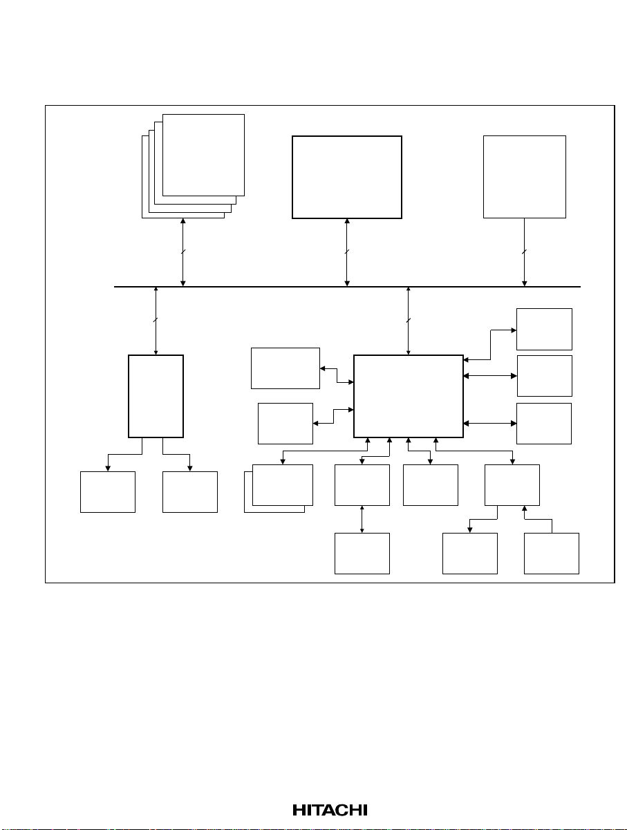
Section 3 System Block Diagram
3.1 Application Circuit
DRAM
SH-4/SH7709
ROM
KEYBOARD
8
Keyboard
Controller
32
TOUCH
PAD
UART
PRINTER
PCMCIA 0
32 32
32
HD64465
STLC7546
DAA
USB
Devices
SPEAKER
CS4218/
CS4271/
AC97
Touch
Panel
IrDA
PS/2
Keyboard
MIC
Rev. 3.0, 03/01, page 7 of 390
Page 27
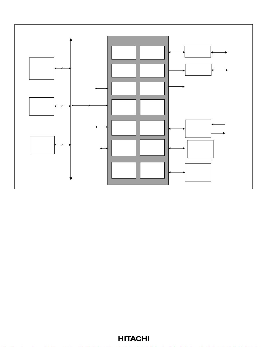
3.2 System Block Diagram
HD64465
Timer & PMU
AFE I/F
STLC7546/7550
AFE
To Public Line
SH-4/SH7709/
SH3-DSP
DRAM
ROM
32
32
32
To Host PC
32
To Host PC
To USB Devices
INTC KBC I/F
UART
Clock Gen &
PLL
IrDA CODEC I/F
USB Host
controller
GPIO(40)
PCMCIA +
Printer I/F
PS/2
Buffers
10-bit ADC
KBC
To Printer
CS4271/
CS4218/AC97
PC Card
PC Card
Touch Panel
To KeyBoard
MIC
SPEAKER
Rev. 3.0, 03/01, page 8 of 390
Page 28

3.3 Physical Address Space
Area 0: H'00000000
Area 1: H'04000000
Area 2: H'08000000
Area 3: H'0C000000
Area 4: H'10000000
Area 5: H'14000000
Area 6: H'18000000
Ordinary memory /
Burst ROM
Internal I/O
Ordinary memory /
SDRAM, DRAM
Ordinary memory /
SDRAM, DRAM, PSRAM
Intelligent Peripheral Controller
Ordinary memory /
Burst ROM / PCMCIA
Ordinary memory /
Burst ROM / PCMCIA
Internal Registers of Intelligent Peripheral
Controller
The PCMCIA interface is shared by the
memory card and I/O card.
The PCMCIA interface is shared by the
memory card and I/O card.
Rev. 3.0, 03/01, page 9 of 390
Page 29
3.4 HD64465 Memory Address
H'10000000H'10000FFF
H'10001000H'10001FFF
H'10002000H'10002FFF
H'10003000H'10003FFF
H'10004000H'10004FFF
H'10005000H'10005FFF
H'10006000H'10006FFF
H'10007000H'10007FFF
H'10008000H'10008FFF
H'10009000H'10009FFF
Standby & System Register
Reserved
PCMCIA Register
AFE I/F Register
GPIO Register
INTC Register
Timer Register
IrDA Register
UART Register
Embeded SRAM
H'1000A000H'1000AFFF
H'1000B000H'1000BFFF
H'1000C000H'1000CFFF
H'1000D000H'1000DFFF
H'1000E000H'1000EFFF
Rev. 3.0, 03/01, page 10 of 390
Paralell Port Register
USB Host Register
Audio Codec I/F Register
KBC Register
ADC I/F Register
Page 30
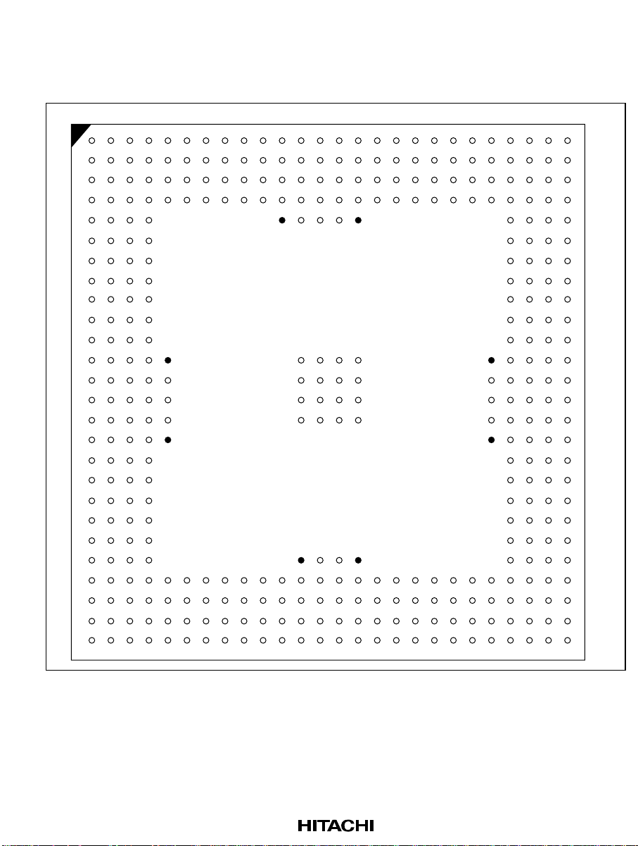
3.5 Pin Configuration
3.5.1 HD64465BP Top View
1 2 3 4 5 6 7 8 9 10 11 12 13 14 15 16 17 18 19 20 21 22 23 24 25 26
RXD0
PC4
PC5
PC6
PCC0
D3
PCC0
D10
PCC0
D2
VCCA
SS3
PC7
PD1
PCC0
A23
PCC0
A24
PCC0
A25
PCC0
D11
AV
AV
PD5
PE5
PE1
PE2
PE3
PE4
PCC0
RESET
PCC0
A13
PCC0
A14
VCCA
PE6
PE7
MSDATA
RDB#
WEB#
PCC0ICI
OWRB#
PCC0IC
IORDB#
MSC
K
KBDATA
KBCK
PWM1
VCC
PCC1
A17
PCC1
D2
PCC1
D13
VCC
PCC0
A12
PCC0
REG#
PCC0
CE2B#
PCC0
CE1B#
CC3
PD2
PD3PD0
PD4
PCC0
A19
PCC0
A20
PCC0
A21
PCC0
A22
PCC0
PCC0
PCC0
A17
PCC0
PD6
PD7
PE0
A15
A16
A18
UCKE
AVSS1
PB1 PB0
PB4
ACPD#
SIBC
SIBD
OUT
TST0
TMS
TDI
AFECK AFECKE BS#
AVSS2
AVCC2
SCLK FS
HC1
AFEP
PA0
DOUT
PA4
XIOW#XIOR#
KBCS#
KBIRQ0
RESE
TPI#
A1 A0 D31
D29
D25
D13
D9
D21
D18
D16
D7
UCK
AVC
C1
PB3 PB2
PB7
LK
AC
RST#
TDO
TRST# TCK
AFER
ST#
DN#
MCLKO
PA3
PA2 PA1
KBIRQ1 P80LE
A12
A11
A7
A8A3A9
A4A5
D28
D27
D15
D24
D12
D11
D23
D8
D20
D19
D17
D4
D6
D3
D2
D5
AVC
C6
USB
D1P
USB
D1M
PB5PB6
ACCLKSIBDIN
SIBSYNC
RING
DIN
OFF
HOOK
PA6PA7
CKIO
A10
A6
A2
D30
D26
D14
D10
D22
D1
D0
IRQ0#
RDY#
VCC5
TSPX
TSPY
AVSS6
VCC
PA5
SH_MODE
VCC
DRAK1
DREQ1#
DRAK0
DRE
Q0#
TSMX
AVCC5
AVSS4
A13
A14
A15
A16
AVCC4TSMY
VCC5
PPD7
A17
A18
A19
ACK#
SLIN#
PPD5PPD6
A21
A22
A23
A24A20
VCC5
SLCT
BUSY
A25
CS4#
RDWR#
RD#
RI0#
PC1
MOD
TXD
RX#
PPD0
USBD
VSS
VSS
VSS
VCC
VCC0
SEL1
VCC0
SEL0
VCC0
VPP1
PC2
SEL
PC3
DCD0#
PC0
DS
USB
DT
R0#
OVR#
R0#
USBD
RTS0#
CTS0#
2P
TXD0
VCC
USBP
EN#
2M
VSSVSSVSS
VSS VSSVSS
VSS
VSS
VSSVSS
VSS VSS
VSS
VCC0
PCC0
VCC
VPP0
WP#
PCC0
PCC0
PCC0
CD2#
PCC0
CD1#
PCC0
PCC0
VS1#
VS2#
WAIT#
PCC0
RDY
PCC0
BVD1
PCC0B
VD2
PCC0
PCC0
PCC0
D9
D1
D8
D0
VCC5
INIT#
PPD1
ERR#
AFD#
PEPPD4
PPD2
PPD3
STB#
VCC
WE0#
CE2A#
IOIS16#
WE1#
CE1A#
CE2B#
WE2#
WE3#
CE1B#
WEA#
PCC1C
RESET
MO#
RESE
TPO#
RESE
TMI#
PWM0
VCC1
VPP1
PCC1
VS2#
PCC1
RDY
E1A#
PCC1
A25
PCC1
A21
PCC1
A16
PCC1
D11
PCC1
D5
PCC1
D15
PCC1
A2
PCC1
A6
PCC1
A9
PCC1
A13
PCC0
D15
PCC0
D13
PCC0
A0
PCC0
A9
PCC0
A10
PCC0
A11
NC
NC
NC
NC
VCC1
VPP0
PCC1
VS1#
PCC1
WP#
PCC1
RESET
RDA#
PCC1
A24
PCC1
A20
PCC1
D8
PCC1
D10
PCC1
D4
PCC1
D6
PCC1
A1
PCC1
A5
PCC1
A8
PCC1
A12
PCC0
D7
PCC0D5PCC0
PCC0
D12
PCC0
A3
PCC0
A8
VCCA
NC
NC
NC
NCNCNC
VCC1
SEL1
PCC1
CD2#
PCC1
BVD2
PCC1
WAIT#
PCC1ICI
OWRA#
PCC1
CE2A#
PCC1
A23
PCC1
A19
PCC1
D0
PCC1
D1
PCC1
D12
PCC1
D14
PCC1
A0
PCC1
A4
PCC1
A7
PCC1
A11
PCC1
A15
D14
PCC0
D4
PCC0
A2
PCC0
A5
PCC0
A7
NC
NC
NC
NC
VCC1
SEL0
PCC1
CD1#
PCC1
BVD1
VCCB
PCC1IC
IORDA#
PCC1
REG#
PCC1
A22
PCC1
A18
VCCB
PCC1
D9
PCC1
D3
VCCB
PCC1
D7
PCC1
A3
VCCB
PCC1
A10
PCC1
A14
PCC0
D6
VCCA
PCC0
A1
PCC0
A4
PCC0
A6
A
B
C
D
E
F
G
H
J
K
L
M
N
P
R
T
U
V
W
Y
AA
AB
AC
AD
AE
AF
Rev. 3.0, 03/01, page 11 of 390
Page 31

3.5.2 HD64465BP Bottom View
26 25 24 23 22 21 20 19 18 17 16 15 14 13 12 11 10 9 8 7 6 5 4 3 2 1
AA
AB
AC
AD
AE
AF
A
B
C
D
E
F
G
PCC1
BVD1/
H
J
PCC1IC
IORDA#
K
L
M
N
P
R
T
U
V
W
Y
PCC0
A4
PCC0
TMO#
NCNCNC RESE
TPO#
TM1#
VCC1
SEL1
SEL0
PCC1
PCC1
CD1#
PCC1BVD
VCCB PCC1
PCC1
REG#
PCC1
A22
PCC1
A18
VCCB PCC1
PCC1
D9
PCC1
D3
VCCB PCC1
PCC1
D7
PCC1
A3
VCCB PCC1
PCC1
A10
PCC1
A14
PCC0
D6
VCCA PCC0
PCC0
A1
PCC0
A6
CD2#
2/SPKR1
PCC1
WAIT#
PCC1IC
IOWRA
CE2A#
PCC1
A23
PCC1
A19
PCC1
D0
PCC1
D1
PCC1
D12
PCC1
D14
PCC1
A0
PCC1
A4
PCC1
A7
PCC1
A11
PCC1
A15
PCC0
D14
PCC0
D4
PCC0
A2
A5
A7
PCC0
VCCAPCC0
VPP0
WP#/
RESET
A24
A20
D10
A12
PCC0
D12
PCC0
A8
D8
D4
D6
A1
A5
A8
D7
D5
A3
VS1#
PCC0
A10
PCC0
VCC1
VPP1
RDY/
PCC1C
E1A#
PCC1
A25
PCC1
A21
A16
PCC1
D11
PCC1
D5
D15
PCC1
PCC1
PCC1
A13
PCC0
D15
PCC0
D13
PCC0
A11
NC
PCC1
VS2#
WEA
A2
A6
A9
A0
A9
#
PCC0
CE2B#
CE1B#
PWM1NCNCNC PWM0
PCC0
REG#
PCC0
ATA
VCC
PCC1
A17
PCC1
PCC1
D13
VCC
A12
D2
ATA
RDB#PCC0
WEB
PCC0ICI
OWRB#
IORDB#
#
PCC0
RESET
PCC0
A13
PCC0
A14
VCCAPCC0IC
PD5PE1PE5MSCKNCNCNC RESE
PCC0
A15
PCC0
A16
PCC0
A17
PCC0
A18
AVCC
PCC0
A19
PCC0
A20
PCC0
A21
PCC0
A22
DTR0
RTS0
TXD0
VSS
VSS
VSS
PCC0
WP#/
PCC0
WAIT#
PCC0
RDY/
PCC0
BVD1/
PCC0
BVD2/
#
#
OVR#
2P
USBP
DN#
VSS VSSVSS
VSS VSS
VCC0
VPP0
PCC0
CD2#
PCC0
CD1#
PCC0
VS2#
VS1#
MOD
SEL
TXDPC7PD2PD6PE2PE6KBD
RX#PD0PD3PD7PE3PE7KBCKNCNCNC RESE
PPD0PD1PD4PE0PE4MSD
USBD
VSSVSSVSS
VSSVSS
VCCVCC
SEL1/
SEL0/
VCC0
VPP1/
PEPPD2DSR0
PPD4AFD# TSMY USB
PPD5STB# AVSS4PB5/KBC
VCC
2M
A21WE0# A13 D1IOIS16#PCC0
WE#
A22WE1#/
A23WE2#/I
R#
A24WE3#/I
CE2B#PCC0
CS5#
CS6#
CIORD#
CIOWR#
AVSS
3
3
PC4 PC0PC3 SLIN#ERR# AVCC5USB
#
PC5 USB
#
PC6 USBD
#
VCC
VSS
VSS
VSS
PCC0
D9
D3
A23
PCC0
PCC0
PCC0
D1
D10
A24
PCC0
PCC0
D8
D2
A25
PCC0
VCCA PCC0
PCC0
D0
D11
4
PPD6BUSYPPD3CTS0
A20RD#CE1B#/
TSPXPPD7SLCTPPD1DCD0
D1P
D1M
S6
_RESUME
SIBSYNCVCC1
DINRDA#PCC1
VCC
PA5
P80LE
SH_M
ODE
VCCPCC1
A14 D0VCC0
A15 IRQ0#VCC0
A16 RDY#/
Q0#
WAIT#
UCKVCC5VCC5VCC5VCC5R10#RXD0 PC1PC2 ACK#INIT# TSMX AVC
AVSS1
UCKE
C6
AVC
PB1/
PB0/
C1
TMO1#
TMO0#
PB2TSPYAVCC
PB4/KB
PB3
WAKEUP#
PB6AVS
ACPD#/
PB7
ACIRQ/
SIBDINACCLKNCVCC1
SIBDO
SIBC
UT
LK
ACRS
TMS
TST
T#
TRSTTCKPCC1
TDI
TDO
AFECKEBS#PCC1
KBIRQ1CKIOPCC1
MCLKORLYPCC1
AFER
ST#
PA2PA1PCC1
PA7PA6PCC1
A11A10PCC1
D31D30PCC1
D27D26PCC1
D15D14PCC1
D11D10PCC0
D23D22PCC0
D19DRAK1A17A25CE2A#PCC0
AVSS2
AFECK
FSRINGPCC1
AVCC2
SCLK
HC1
AFEP
DN#
PA0
DOUT
PA4
PA3
XIOR#
XIOW#
KBCS#
KBIRQ0
RESET#
A12
A7A6
A9
A8
A3A2PCC1
A5
A4
A1
A0
D29
D28
D25
D24
D13
D12
D9
D8
D21
D20
D4DREQ1#A18CS4#CE1A#/
D18
D17
D3DRAK0A19RDW
D16
D6
D2DRE
D7
D5
Rev. 3.0, 03/01, page 12 of 390
Page 32

3.5.3 HD64465BQ Top View
1 2 3 4 5 6 7 8 9 10 11 12 13 14 15 16 17 18 19 20
A
B
C
D
E
F
G
H
J
K
L
M
N
P
R
T
U
V
W
Y
PB0
PB4 ACPD#
ACR
ST#
TDO
AFE
CKE
FS
HC1
PA0
PA3
PA5
KBI
RQ0
P80LE
A8
A6
A0
D28
D24
D10
D23
D19
UCKE
SIB
DIN
TST
TDI
RING
AFE
RST#
DOUT
PA2
PA6
KBCS#
CKIO
A7
A3
D29
D27
D15
D9
D21
D6
AVCC6
UCK
PB3
OFFH
OOK
PA1
KBIRQ1XIOW#
DRAK0D5
TSMY
TSPY
USB
D1P
PB1ACCLK
PB6TRST#
PB7BS#
TMSAVCC2
AFE
CK
AFEP
DN#
PA4PA7
A5A11
D31A4
D25D30
D11D26
D16D13
D17D8
D3D20
A13IRQ0#
PPD4
VCC5
TSMX
SYNC
WAIT#
USB
D1M
CLK
A12
SIB
KO
BUSY
ACK#
TSPX
AVSS6AVSS1
PB2PB5
SIBD
OUT
TCKSIB
AVSS2SCLK
XIOR#MCL
RESE
TPI#
D14D12
A17RDY#/
A20A15
A23A19
PE2
PE4
KBCK
NC
NC
NC
VCC1
VPP0
PCC1
WP#
PCC1
PCC1
A16
PCC1
D14
PCC1
A2
PCC1
A9
PCC0
D13
PCC0
A3
PCC0
A8
PCC0
A7
PCC0
A12
PCC0
VCCA
PE6
RESE
TMO#
NC
NC
VCC1
SEL1
PCC1
VS1#
PCC1
ICIOWRA#
PCC1
A24
PCC1
D0
PCC1
D13
PCC1
A3
PCC1
A10
PCC1
A15
PCC0
D4
PCC0
A1
PCC0
A5
VCCA
PCC0
CE2B#
PCC0
CE1B#
KBD
ATA
NC
NCNC
VCC1
VPP1
PCC1
BVD2
PCC1
WAIT#
WEA#
PCC1
A23
PCC1
A20
PCC1
D9
PCC1
D10
PCC1
D5
PCC1
D7
PCC1
A6
PCC0
A14
PCC0
D15
PCC0
D14
PCC0
D12
PCC0
A4
PCC0
A11
NC
NC
VCC
SEL0
PCC1
VS2#
VCCB
IRIORDA#
PCC1
CE2A#
PCC1
A22
PCC1
A19
VCCB
PCC1
D2
PCC1
D4
D6
PCC1
A0
VCCB
PCC1
A8
PCC1
A12
PCC0
D6
PCC0
A0
PCC0
A6
NC
NC
PCC
CD1#
PCC1
BVD1
PCC1
RESET
RDA#PCC1
PCC1
REG#
PCC1
A21
PCC1
A18
PCC1
D8
PCC1
D11
PCC1
D3
VCCBPCC1
PCC1
D15
PCC1
A4
PCC1
A7
PCC1
A11
PCC0
D7
PCC0
D5
PCC0
A2
PD5
PC5
DSR0#
CTS0#
RXD0
PD2
PD3
DCD0#
VSS
VSS
VSS
VSS
PCC0
A19
PCC0
A21
PCC0
D9
PCC0
D2
PCC0
A22
VCCA
PCC0
D8
PCC0
D0
PC6
PD1
PD4
PE1PD7
MSD
ATA
MSCKPE3
RESE
TMI#
PCC0
REG#
PCC0
RESET
PCC0
A14
PCC0
D11
PCC0
A18
PCC0
A24
PCC0
D3
PCC0
D10
PC7
AVCC3
PD6
PE5
RESE
TPO#
PWM0
VCC3
VCC3
PCC1
A17
PCC1
A1
VCC3
VCC3
PCC0
A13
RDB#
PCC0
A15
PCC0
A17
PCC0
A23
PCC0
A25
PE0
PE7
PWM1
NC
NC
PCC1
CD2#
PCC1
RDY
PCC1
A25
PCC1
D1
PCC1
D12
PCC1
A5
PCC1
A13
VCCA
PCC0
A9
PCC0
A10
WEB#
PCC0
IRIOWRB#
PCC0
A16
PCC0
A20
CE1A#
ICIORDB#
PC2
USB
PPD1
STB#
USB
PEN#
D2M
RTS0#
PC0
PPD0
ERR#
SLCT
VCC5PPD7
SLIN#
PPD5VCC5
AVSS4VCC3
AVCC1
D1VCC3
A18DREQ1#
A16DRAK1
A22A14
A25A21
WE2#RD#
WE3#WE0#
TXDPPD2
VCC5
INT#
DREQ0#
RDWR#
CS4#
CE2A#
CE1A#
CE1B#
IOIS16#
USB
OVR#
USB
D2P
MODSEL
/RX2#
PC1PPD3
RX#AFD#
DTR0#AVCC5
VSSVSS
VSSVSS
VSSVSS
VSSVSS
WE1#
CE2B#A24
VCC0
SEL0
VCC0
SEL1
PCC0
VS2#
PCC0
CD1#
PCC0
CD2#
VCC0
VPP1
PC3
PD0
TXD0
PC4
RI0#
AVSS3
VSS
VSS
VSS
VSS
VCC0
VPP0
PCC0
D1
PCC0
WP#
PCC0
VS1#
PCC0
WAIT#
PCC0
BVD2
PCC0
BVD1
PCC0
RDY
PEPPD6
AVCC4
VCC3
DIN
SH_
MODE
A9A10
VCC3
A1A2
D7D22
D2D18
D0D4
Rev. 3.0, 03/01, page 13 of 390
Page 33

3.5.4 HD64465BQ Bottom View
2019181716151413121110987654321
KBD
NC
NC NC
PCC
CD1#
PCC1
BVD1
PCC1
RESET
RDA#
PCC1
REG#
PCC1
A21
PCC1
A18
PCC1
D8
PCC1
D11
PCC1
D3
VCCB
PCC1
D15
PCC1
A4
PCC1
A7
PCC1
A11
PCC0
D7
PCC0
D5
PCC0
A2
2019181716151413121110987654321
NC
VCC
SEL0
PCC1
VS2#
VCCB
PCC1
IRIORDA#
PCC1
CE2A#
PCC1
A22
PCC1
A19
VCCB
PCC1
D2
PCC1
D4
PCC1
D6
PCC1
A0
VCCB
PCC1
A8
PCC1
A12
PCC0
D6
PCC0
A0
PCC0
A6
ATA
NC
NC
VPP1
BVD2
PCC1
WAIT#
WEA#
PCC1
A23
PCC1
A20
PCC1
D9
PCC1
D10
D5
PCC1
D7
PCC1
A6
PCC0
A14
PCC0
D15
PCC0
D14
D12
PCC0
A4
PCC0
A11
PE6
RESE
TMO#
NC
NCVCC1
NCPCC1
VCC1
SEL1
PCC1
VS1#
PCC1
ICIOWRA#
PCC1
A24
PCC1
D0
PCC1
D13
A3PCC1
PCC1
A10
PCC1
A15
PCC0
D4
PCC0
A1
PCC0
A5
VCCAPCC0
PCC0
CE2B#
PCC0
CE1B#
PE2
PE4
KBCK
NC
PCC1
VPP0
PCC1
WP#
PCC1
CE1A#
PCC1
A16
PCC1
D14
PCC1
A9
D13
PCC0
A3
PCC0
A8
A7
PCC0
A12
PCC0
ICIORDB#
VCCA
PD5
PE0
PWM1
NCNC
NCNC
PCC1
CD2#
PCC1
RDY
PCC1
A25
PCC1
D1
PCC1
D12
A5A2
PCC1
A13
VCCAPCC0
PCC0
A9
PCC0
A10
WEB#PCC0
PCC0
IRIOWRB#
PCC0
A16
PCC0
A20
PC7
AVCC3
PD6PE7
TPO#
PWM0
VCC3
PCC1
A17
PCC1
VCC3
VCC3
PCC0
A13
RDB#
PCC0
A15
PCC0
A17
PCC0
A23
PCC0
A25
PPD4
VCC5
TSMX
USB
D1M
AVSS1
PB5
SIB
CLK
SIB
SYNC
SLCK
MCLKO
A12
A10
A2
D12
D22
D18
D4
RDY#/
WAIT#
A15
A19
TSMY
TSPY
D1P
PB1
PB6
PB7
TMS
AFECK
AFEP
DN#
PA4
KBI
RQ1
A5
D31
D25
D11
D16
D17
D3
DRAK0
A13
AVCC6
UCK
PB3USB
ACCLK
TRST
BS#
AVCC2
OFFH
OOK
PA1
PA7
XIOW#
A11
A4
D30
D26
D13
D8
D20
D5
IRQ0#
UCKE
ACPD#
SIB
DIN
TST
TDI
RST#
KBCS#
D2M
PPD0
TXD
VCC5
VSS
VSS
VSS
VSS
DREQ0#
VCS5
SLIN#INIT#
PPD5PPD3
AVSS4AFD#
AVCC1AVCC5
WE2#CE1B#
WE3#IOIS16#
ERR#
PPD2
D1A24
A18RDWR#
A16CS4#
A22CE2A#
A25CE1A#
STB#
SLCT
PE
PPD7
AVCC4
VCC5
VCC3
VCC3
DIN
SH_
MODE
VCC3
VCC3
DREQ1#
DRAK1
A14
A21
RD#
WE0#
ACK#
PPD6
TSPX
AVSS6
PB2
SIBD
OUT
TCK
AVSS2
XIOR#
RESE
TPI#
A9
A1
D14
D7
D2
D0
A17
A20
A23
USB
PC2
PC5
DSR0#
PEN#
RTS0#
RXD0PD1
PD2
PCC0
A19
PCC0
A21
PCC0
D9
PCC0
D2
PCC0
A22
VCCA
PCC0
D8
PCC0
D0
PC3
PD0
TXD0PD7
PC4PD3
RI0#PE3
AVSS3DCD0#
VSSVSS
VSSVSS
VSSVSS
VSSVSS
VCC0
VPP0
PCC0
PCC0
WP#
PCC0
VS1#
PCC0
WAIT#
PCC0
BVD2
PCC0
BVD1
PCC0
RDY
D1
PC0
USB
OVR#
USB
D2P
MODSEL
/RX2#
PC1
RX#
DTR0#
VSS
VSS
VSS
VSS
WE1#
CE2B#
VCC0
SEL0
VCC0
SEL1
PCC0
VS2#
PCC0
CD1#
PCC0
CD2#
VCC0
VPP1
CTS0#
PC6
PD4PE5
PE1RESE
MSD
ATA
MSCKVCC3
RESE
TMI#
A1
PCC0
REG#
PCC0
RESET
PCC0
A14
PCC0
D11
PCC0
A18
PCC0
A24
PCC0
D3
PCC0
D10
BUSY
PPD1
USB
A
PB0
B
PB4
C
ACR
ST#
D
TDO
E
AFE
CKE
F
FSRING
G
HC1AFE
H
PA0DOUT
J
PA3PA2
K
PA5PA6
L
KBI
RQ0
M
P80LECKIO
N
A8A7
P
A6A3
R
A0D29
T
D28D27
U
D24D15
V
D10D9
W
D23D21
Y
D19D6
Rev. 3.0, 03/01, page 14 of 390
Page 34

Section 4 Pin Description
Table 4.1 HD64465BP Signal Names (by pin numbers in alphabetical order)
Pin Signal Pin Signal Pin Signal Pin Signal
A1 AVSS1 B1 PB1/TMO1# C1 PB4/KBWAKEUP# D1 ACPD#/ACIRQ/
PWE#
A2 UCKE B2 PB0/TMO0# C2 PB3 D2 PB7
A3 UCK B3 AVCC1 C3 PB2 D3 PB6
A4 AVCC6 B4 USBD1P C4 USBD1M D4 PB5/KBRESUME
A5 VCC5 B5 TSPX C5 TSPY D5 AVSS6
A6 TSMX B6 AVCC5 C6 TSMY D6 AVSS4
A7 VCC5 B7 PPD7 C7 AVCC4 D7 PPD6
A8 ACK# B8 SLIN# C8 PPD4 D8 PPD5
A9 VCC5 B9 SLCT C9 PE D9 BUSY
A10 INIT# B10 ERR# C10 AFD# D10 STB#
A11 VCC5 B11 PPD1 C11 PPD2 D11 PPD3
A12 MODSEL/RX2# B12 TXD C12 RX# D12 PPD0
A13 PC1 B13 PC0 C13 USBOVR# D13 USBD2P
A14 PC2 B14 PC3 C14 DTR0# D14 RTS0#
A15 RI0# B15 DCD0# C15 DSR0# D15 CTS0#
A16 RXD0 B16 PC4 C16 PC5 D16 PC6
A17 AVSS3 B17 PC7 C17 PD0 D17 PD1
A18 AVCC3 B18 PD2 C18 PD3 D18 PD4
A19 PD5 B19 PD6 C19 PD7 D19 PE0
A20 PE1 B20 PE2 C20 PE3 D20 PE4
A21 PE5 B21 PE6 C21 PE7 D21 NC
A22 MSCK B22 KBDATA C22 KBCK D22 PWM1
A23 RESETMO# B23 RESETPO# C23 RESETMI# D23 PWM0
A24 NC B24 NC C24 NC D24 NC
A25 NC B25 NC C25 NC D25 NC
A26 NC B26 NC C26 NC D26 NC
Rev. 3.0, 03/01, page 15 of 390
Page 35

Table 4.1 HD64465BP Signal Names (by pin numbers in alphabetical order) [cont’d]
Pin Signal Pin Signal Pin Signal Pin Signal
E1 SIBDOUT G1 TDI J1 AVCC2 L1 PA0
E2 SIBCLK G2 TDO J2 SCLK L2 DOUT
E3 SIBDIN G3 TRST J3 FS L3 MCLKO
E4 ACCLK G4 TCK J4 RING L4 OFFHOOK/RLY
E11 VCC G23 PCC1VS2# J23 WEA# L23 PCC1A25
E12 USBD2M G24 PCC1VS1# J24 PCC1RESET L24 PCC1A24
E13 USBPEN# G25 PCC1BVD2/SPKR1 J25 PCC1ICIOWRA#L25 PCC1A23
E14 TXD0 G26 PCC1BVD1/STSCHG1# J26 PCC1ICIORDA# L26 PCC1A22
E15 VCC
E23 NC H1 AVSS2 K1 HC1 M1 PA4
E24 NC H2 AFECK K2 AFEPDN# M2 PA3
E25 VCC1SEL1 H3 AFECKE K3 AFERST# M3 PA2
E26 VCC1SEL0 H4 BS# K4 DIN M4 PA1
H23 PCC1RDY/IREQ1# K23 PCC1CE1A# M5 VCC
F1 TMS H24 PCC1WP#/IOIS16# K24 RDA# M12 VSS
F2 TST H25 PCC1WAIT# K25 PCC1CE2A# M13 VSS
F3 ACRST# H26 VCCB K26 PCC1REG# M14 VSS
F4 SIBSYNC M15 VSS
F23 VCC1VPP1 M22 VCC
F24 VCC1VPP0 M23 PCC1A21
F25 PCC1CD2# M24 PCC1A20
F26 PCC1CD1# M25 PCC1A19
M26 PCC1A18
Rev. 3.0, 03/01, page 16 of 390
Page 36

Table 4.1 HD64465BP Signal Names (by pin numbers in alphabetical order) [cont’d]
Pin Signal Pin Signal Pin Signal Pin Signal
N1 XIOR# R1 RESETPI# U1 A5 W1 D29
N2 XIOW# R2 A12 U2 A4 W2 D28
N3 PA7 R3 A11 U3 A3 W3 D27
N4 PA6 R4 A10 U4 A2 W4 D26
N5 PA5 R5 SH_MODE U23 PCC1A2 W23 PCC1A9
N12 VSS R12 VSS U24 PCC1A1 W24 PCC1A8
N13 VSS R13 VSS U25 PCC1A0 W25 PCC1A7
N14 VSS R14 VSS U26 PCC1D7 W26 VCCB
N15 VSS R15 VSS
N22 PCC1A17 R22 PCC1D13 V1 A1 Y1 D25
N23 PCC1A16 R23 PCC1D5 V2 A0 Y2 D24
N24 PCC1D8 R24 PCC1D4 V3 D31 Y3 D15
N25 PCC1D0 R25 PCC1D12 V4 D30 Y4 D14
N26 VCCB R26 PCC1D3 V23 PCC1A6 Y23 PCC1A13
V24 PCC1A5 Y24 PCC1A12
P1 KBCS# T1 A9 V25 PCC1A4 Y25 PCC1A11
P2 KBIRQ0 T2 A8 V26 PCC1A3 Y26 PCC1A10
P3 KBIRQ1 T3 A7
P4 CKIO T4 A6
P5 P80LE T5 VCC
P12 VSS T22 VCC
P13 VSS T23 PCC1D15
P14 VSS T24 PCC1D6
P15 VSS T25 PCC1D14
P22 PCC1D2 T26 VCCB
P23 PCC1D11
P24 PCC1D10
P25 PCC1D1
P26 PCC1D9
Rev. 3.0, 03/01, page 17 of 390
Page 37

Table 4.1 HD64465BP Signal Names (by pin numbers in alphabetical order) [cont’d]
Pin Signal Pin Signal Pin Signal Pin Signal
AA1 D13 AC1 D21 AD1 D18 AE1 D16
AA2 D12 AC2 D20 AD2 D17 AE2 D6
AA3 D11 AC3 D19 AD3 D4 AE3 D3
AA4 D10 AC4 D1 AD4 D0 AE4 IRQ0#
AA23 PCC0D15 AC5 DRAK1 AD5 DREQ1# AE5 DRAK0
AA24 PCC0D7 AC6 A13 AD6 A14 AE6 A15
AA25 PCC1A15 AC7 A17 AD7 A18 AE7 A19
AA26 PCC1A14 AC8 A21 AD8 A22 AE8 A23
AC9 A25 AD9 CS4# AE9 RDWR#
AB1 D9 AC10 WE0# AD10 WE1#/WE# AE10 WE2#/ICIORD#
AB2 D8 AC11 CE2A# AD11 CE1A#/CS5# AE11 CE2B#
AB3 D23 AC12 IOIS16# AD12 VCC0SEL1/
CLOCK
AB4 D22 AC13 PCC0CD2# AD13 PCC0CD1# AE13 PCC0VS2#
AB12 VCC AC14 PCC0WAIT# AD14 PCC0RDY/
IREQ0#
AB13 VCC0VPP0 AC15 PCC0D9 AD15 PCC0D1 AE15 PCC0D8
AB14 PCC0WP#/IOIS16B AC16 PCC0D3 AD16 PCC0D10 AE16 PCC0D2
AB15 VCC AC17 PCC0D23 AD17 PCC0A24 AE17 PCC0A25
AB23 PCC0D13 AC18 PCC0A19 AD18 PCC0A20 AE18 PCC0A21
AB24 PCC0D5 AC19 PCC0A15 AD19 PCC0A16 AE19 PCC0A17
AB25 PCC0D14 AC20 PCC0RESET AD20 PCC0A13 AE20 PCC0A14
AB26 PCC0D6 AC21 RDB# AD21 WEB# AE21 PCC0ICIOWRB#
AC22 PCC0A12 AD22 PCC0REG# AE22 PCC0CE2B#
AC23 PCC0A0 AD23 PCC0A9 AE23 PCC0A10
AC24 PCC0D12 AD24 PCC0A3 AE24 PCC0A8
AC25 PCC0D4 AD25 PCC0A2 AE25 PCC0A5
AC26 VCCA AD26 PCC0A1 AE26 PCC0A4
AE12 VCC0SEL0/
DATA
AE14 PCC0BVD1/
STSCHG0#
Rev. 3.0, 03/01, page 18 of 390
Page 38

Table 4.1 HD64465BP Signal Names (by pin numbers in alphabetical order) [cont’d]
Pin Signal Pin Signal Pin Signal
AF1 D7 AF11 CE1B#/CS6# AF21 PCC0ICIORDB#
AF2 D5 AF12 VCC0VPP1/LATCH AF22 PCC0CE1B#
AF3 D2 AF13 PCC0VS1# AF23 PCC0A11
AF4 RDY#/WAIT# AF14 PCC0BVD2/SPKR0 AF24 VCCA
AF5 DREQ0# AF15 PCC0D0 AF25 PCC0A7
AF6 A16 AF16 VCCA AF26 PCC0A6
AF7 A20 AF17 PCC0D11
AF8 A24 AF18 PCC0A22
AF9 RD# AF19 PCC0A18
AF10 WE3#/ICIOWR# AF20 VCCA
Rev. 3.0, 03/01, page 19 of 390
Page 39

Table 4.2 HD64465BQ Signal Names (by pin numbers in alphabetical order)
Pin Signal Pin Signal Pin Signal Pin Signal
A1 PB0/TMO0 B1 PB4/KBWAEUP# C1 ACRST# D1 TDO
A2 UCKE B2 ACPD#/ACIRQ C2 SIBDIN D2 TST
A3 AVCC6 B3 UCK C3 PB3 D3 ACCLK
A4 TSMY B4 TSPY C4 USBD1P D4 PB1/TMO1#
A5 PPD4 B5 VCC5 C5 TSMX D5 USBD1M
A6 BUSY B6 ACK# C6 PPD6 D6 TSPX
A7 STB# B7 SLCT C7 PE D7 PPD7
A8 PDD1 B8 ERR# C8 PPD2 D8 VCC5
A9 USBD2M B9 PPD0 C9 TXD D9 VCC5
A10 USBPEN# B10 PC0 C10 USBOVR# D10 USBD2P
A11 PC2 B11 RTS0# C11 PC3 D11 PD0
A12 DSR0# B12 CTS0# C12 RXD0 D12 PD2
A13 PC5 B13 PC6 C13 PD1 D13 PD4
A14 PC7 B14 AVCC3 C14 PD6 D14 PE5
A15 PD5 B15 PE0 C15 PE7 D15 PWM1
A16 PE2 B16 PE4 C16 KBCK D16 NC
A17 PE6 B17 RESETMO# C17 NC D17 NC
A18 KBDATA B18 NC C18 NC D18 VCC1VPP1
A19 NC B19 NC C19 VCC1SEL0 D19 PCC1VS2#
A20 NC B20 NC C20 PCC1CD1# D20 PCC1BVD1/STSC
HG1#
Rev. 3.0, 03/01, page 20 of 390
Page 40

Table 4.2 HD64465BQ Signal Names (by pin numbers in alphabetical order) [cont’d]
Pin Signal Pin Signal Pin Signal Pin Signal
E1 AFECKE F1 FS G1 HC1 H1 PA0
E2 TDI F2 RING G2 AFERST# H2 DOUT
E3 TRST# F3 BS# G3 AVCC2 H3 OFFHOOK/RLY
E4 PB6 F4 PB7 G4 TMS H4 AFECK
E5 AVSS1 F5 PB5/KBRESUMEG5 SIBCLK H5 SIBSYNC
E6 AVSS6 F6 PB2 G6 SIBDOUT H6 TCK
E7 AVCC4 F7 VCC5 G7 VCC3 H8 AVCC1
E8 SLIN# F8 PPD5 G8 AVSS4 H9 AVCC5
E9 INIT# F9 PPD3 G9 AFD# H10 DTR0#
E10 MODSEL/RX2# F10 PC1 G10 RX# H11 AVSS3
E11 TXD0 F11 PC4 G11 RI0# H12 DCD0#
E12 PD7 F12 PD3 G12 PE3 H13 RESETMI#
E13 PE1 F13 MSDATA G13 MSCK H15 PCC1RDY/IREQ
1#
E14 RESETPO# F14 PWM0 G14 VCC3 H16 PCC1WP#/IOIS
16#
E15 NC F15 NC G15 PCC1CD2# H17 PCC1ICIOWRA#
E16 NC F16 NC G16 VCC1VPP0 H18 PCC1A23
E17 NC F17 VCC1SEL1 G17 PCC1VS1# H19 PCC1A22
E18 PCC1BVD2/SPKR1F18 PCC1WAIT# G18 WEA# H20 PCC1A21
E19 VCCB F19 PCC1ICIORDA#G19 PCC1CE2A#
E20 PCC1RESET F20 RDA# G20 PCC1REG#
Rev. 3.0, 03/01, page 21 of 390
Page 41

Table 4.2 HD64465BQ Signal Names (by pin numbers in alphabetical order) [cont’d]
Pin Signal Pin Signal Pin Signal Pin Signal
J1 PA3 K1 PA5 L1 KBIRQ0 M1 P80LE
J2 PA2 K2 PA6 L2 KBCS# M2 CKIO
J3 PA1 K3 PA7 L3 XIOW# M3 A11
J4 AFEPDN# K4 PA4 L4 KBIRQ1 M4 A5
J5 SCLK K5 MCLKO L5 A12 M5 A10
J6 AVSS2 K6 XIOR# L6 RESETPI# M6 A9
J7 VCC3 K7 DIN L7 SH_MODE M7 VCC3
J9 VSS K9 VSS L9 VSS M9 VSS
J10 VSS K10 VSS L10 VSS M10 VSS
J11 VSS K11 VSS L11 VSS M11 VSS
J12 VSS K12 VSS L12 VSS M12 VSS
J14 VCC3 K14 PCC1A17 L14 PCC1A1 M14 VCC3
J15 PCC1A25 K15 PCC1D1 L15 PCC1D12 M15 PCC1A5
J16 PCC1CE1A# K16 PCC1A1 6 L16 PCC1D14 M16 PCC1A2
J17 PCC1A24 K17 PCC1D0 L17 PCC1D13 M17 PCC1A3
J18 PCC1A20 K18 PCC1D9 L18 PCC1D10 M18 PCC1D5
J19 PCC1A19 K19 VCCB L19 PCC1D2 M19 PCC1D4
J20 PCC1A18 K20 PCC1D8 L20 PCC1D11 M20 PCC1D3
Rev. 3.0, 03/01, page 22 of 390
Page 42

Table 4.2 HD64465BQ Signal Names (by pin numbers in alphabetical order) [cont’d]
Pin Signal Pin Signal Pin Signal Pin Signal
N1 A8 P1 A6 R1 A0 T1 D28
N2 A7 P2 A3 R2 D29 T2 D27
N3 A4 P3 D30 R3 D26 T3 D13
N4 D31 P4 D25 R4 D11 T4 D16
N5 A2 P5 D12 R5 D22 T5 D18
N6 A1 P6 D14 R6 D7 T6 D2
N9 DREQ0# P7 VCC3 R7 DREQ1# T7 DRAK1
N10 WE1#/WE# P8 D1 R8 A18 T8 A16
N11 VCC0VPP0 P9 A24 R9 RDWR# T9 CS4#
N12 PCC0A19 P10 CE2B# R10 VCC0SEL0/
DATA
N13 PCC0REG# P11 PCC0D1 R11 PCC0WP#/
IOIS16
N15 PCC1A13 P12 PCC0A21 R12 PCC0D9 T12 PCC0D2
N16 PCC1A9 P13 PCC0RESET R13 PCC0A14 T13 PCC0D11
N17 PCC1A10 P14 VCC3 R14 PCC0A13 T14 RDB#
N18 PCC1D7 P15 VCCA R15 PCC0A9 T15 PCC0A10
N19 PCC1D6 P16 PCC0D13 R16 PCC0A3 T16 PCC0A8
N20 VCCB P17 PCC1A15 R17 PCC0D4 T17 PCC0A1
P18 PCC1A6 R18 PCC1A14 T18 PCC0D15
P19 PCC1A0 R19 VCCB T19 PCC1A8
P20 PCC1D15 R20 PCC1A4 T20 PCC1A7
T10 VCC0SEL1/
CLOCK
T11 PCC0VS1#
Rev. 3.0, 03/01, page 23 of 390
Page 43

Table 4.2 HD64465BQ Signal Names (by pin numbers in alphabetical order) [cont’d]
Pin Signal Pin Signal Pin Signal Pin Signal
U1 D24 V1 D10 W1 D23 Y1 D19
U2 D15 V2 D9 W2 D21 Y2 D6
U3 D8 V3 D20 W3 D5 Y3 IRQ0#
U4 D17 V4 D3 W4 DRAK0 Y4 A13
U5 D4 V5 RDY#/WAIT# W5 A15 Y5 A19
U6 D0 V6 A17 W6 A20 Y6 A23
U7 A14 V7 A21 W7 RD# Y7 WE0
U8 A22 V8 A25 W8 WE2#/ICIORD#Y8 WE3#/ICIOWR
#
U9 CE2A# V9 CE1A#/CS5# W9 CE1B#/CS6# Y9 IOIS16#
U10 PCC0VS2# V10 PCC0CD1# W10 PCC0CD2# Y10 VCC0VPP1/
LATCH
U11 PCC0WAIT# V11 PCC0BVD2/SPKR0W11 PCC0BVD1/
STSCHG0#
U12 PCC0A22 V12 VCCA W12 PCC0D8 Y12 PCC0D0
U13 PCC0A18 V13 PCC0A24 W13 PCC0D3 Y13 PCC0D10
U14 PCC0A15 V14 PCC0A17 W14 PCC0A23 Y14 PCC0A25
U15 WEB# V15 PCC0ICIOWRB W15 PCC0A16 Y15 PCC0A20
U16 PCC0A7 V16 PCC0A12 W16 PCC0ICIORDB#Y16 VCCA
Y11 PCC0RDY/
IREQ0#
U17 PCC0A5 V17 VCCA W17 PCC0CE2B# Y17 PCC0CE1B#
U18 PCC0D14 V18 PCC0D12 W18 PCC0A4 Y18 PCC0A11
U19 PCC1A12 V19 PCC0D6 W19 PCCA0 Y19 PCC0A6
U20 PCC1A11 V20 PCC0D7 W20 PCC0D5 Y20 PCC0A2
Rev. 3.0, 03/01, page 24 of 390
Page 44

Table 4.3 Pin Descriptions of Test Mode Select
Pin No.
(HD64465BP)
Test Mode
F2 D2 TST I Test Mode Enable
G1 E2 TDI I Boundary Scan Data Input
G2 D1 TDO O Boundary Scan Data Output
F1 G4 TMS I Boundary Scan Mode Select.
G4 H6 TCK I Boundary Scan Clock.
G3 E3 TRST I Boundary Scan Reset
Pin No.
(HD64465BQ) Symbol I/O Description
0 = Disabled
1 = Enabled
This pin can be floating when not using.
This pin can be floating when not using.
This pin can be floating when not using.
Table 4.4 Pin Descriptions of CPU Interface
Pin No.
(HD64465BP)
CPU Interface
P4 M2 CKIO I System clock
AC9, AF8,
AE8, AD8,
AC8, AF7,
AE7, AD7,
AC7,AF6,
AE6, AD6,
AC6, R2-4,T14,
U1-4,V1-2
V3-4, W1-4,
Y1-2, AB3-4,
AC1-3,
AD1-2, AE1,
Y3-4, AA1-4,
AB1-2, AF1,
AE2, AF2,
AD3, AE3,
AF3, AC4, AD4
Pin No.
(HD64465BQ)
V8, P9, Y6, U8,
V7, W6, Y5,
R8, V6, T8,
W5, U7, Y4,
L5, M3, M5,
M6, N1, N2,
P1, M4, N3,
P2, N5, N6, R1
N4, P3, R2, T1,
T2, R3, P4, U1,
W1, R5, W2,
V3, Y1, T5, U4,
T4, U2, P6, T3,
P5, R4, V1, V2,
U3, R6, Y2,
W3, U5, V4,
T6, P8, U6
Symbol I/O Description
A25-A0 I Address bus of CPU
D31-D0 IO Data bus of CPU
Rev. 3.0, 03/01, page 25 of 390
Page 45

Table 4.4 Pin Descriptions of CPU Interface (cont’d)
Pin No.
(HD64465BP)
Pin No.
(HD64465BQ) Symbol I/O Description
AD9 T9 CS4# I Chip select 4 of CPU
AC10 Y7 WE0# I D7-D0 write strobe signal
AD10 N10 WE1#/WE# I D15-D8 write strobe signal, or PCMCIA write
strobe signal
AE10
W8 WE2#/ICIORD#
I D23-D16 write strobe signal, or PCMCIA I/O
READ
AF10
Y8 WE3#/ICIOWR#
I D31-D24 write strobe signal, or PCMCIA I/O
WRITE
AE9 R9 RDWR# I Data bus direction indicator signal
AF9 W7 RD# I Strobe signal indicating the READ cycle
AF4 V5 RDY#/WAIT# O RDY# signal for SH4 / WAIT# signal for
SH7709
H4 F3 BS# I Bus start of CPU
R1 L6 RESETPI# I RESET request
AF5 N9 DREQ0# O DMA request is generated by FIR
AD5 R7 DREQ1# O DMA request is generated by Timer or
Codec interface module
AE5 W4 DRAK0 I DMA request acknowledge for DREQ0#
AC5 T7 DRAK1 I DMA request acknowledge for DREQ1#
AE4 Y3 IRQ0# O Interrupt request to CPU.
R5 L7 SH_MODE I SH7709/SH4 CPU interface selection.
0 = SH7709
1 = SH4
AF11 W9 CE1B#/CS6# I Chip enable 1 for PCMCIA card 0
AE11 P10 CE2B# I Chip enable 2 for PCMCIA card 0
AD11 V9 CE1A#/CS5# I Chip enable 1 for PCMCIA card 1
AC11 U9 CE2A# I Chip enable 2 for PCMCIA card 1
AC12 Y9 IOIS16# O Write protect I/O is 16 bits for PCMCIA card
Rev. 3.0, 03/01, page 26 of 390
Page 46

Table 4.5 Pin Descriptions of PCMCIA 0 Interface
Pin No.
(HD64465BP)
Pin No.
(HD64465BQ) Symbol I/O Description
PCMCIA 0 (memory and IO)
AE17, AD17,
AC17, AF18,
AE18, AD18,
AC18, AF19,
AE19, AD19,
AC19, AE20,
AD20, AC22,
AF23, AE23,
AD23, AE24,
AF25, AF26,
AE25, AE26,
Y14, V13,
W14, U12,
P12, Y15, N12,
U13, V14,
W15, U14,
R13, R14, V16,
Y13, T15, R15,
T16, U16, Y19,
U17, W18,
R16, Y20, T17,
W19
PCC0A25-A0 O Address bus [25:0] of PCMCIA card 0
AD24-26,
AC23
AA23, AB25,
AB23, AC24,
AF17, AD16,
AC15, AE15,
AA24, AB26,
AB24, AC25,
AC16, AE16,
T18, U18, P16,
V18, T13, Y13,
R12, W12,
V20, V19,
W20, R17,
W13, T12,
P11, Y12
PCC0D15-D0 IO Data bus [15:0] of PCMCIA card 0
AD15, AF15
AF22 Y17 PCC0CE1B# O PCMCIA card 0 low byte enable
AE22 W17 PCC0CE2B# O PCMCIA card 0 high byte enable
AC21 T14 RDB# O PCMCIA card 0 Read enable
AD21 U15 WEB# O PCMCIA card 0 Write enable
AF21 W16
AE21
V15 PCC0ICIOWRB#
PCC0ICIORDB#
O PCMCIA card 0 I/O Read enable
O PCMCIA card 0 I/O Write enable
AC20 P13 PCC0RESET O PCMCIA card 0 reset
AC14 U11 PCC0WAIT# I PCMCIA card 0 memory or I/O wait state
Rev. 3.0, 03/01, page 27 of 390
Page 47

Table 4.5 Pin Descriptions of PCMCIA 0 Interface (cont’d)
Pin No.
(HD64465BP)
AB14 R11 PCC0WP#/
AD14 Y11 PCC0RDY/
AE14 W11 PCC0BVD1/
AF14 V11 PCC0BVD2/
AD13 V10 PCC0CD1# I Provides for PCMCIA card 0 insertion
AC13 W10 PCC0CD2# I Provides for PCMCIA card 0 insertion
AF13 T11 PCC0VS1# I PCMCIA card 0 Voltage sense
AE13 U10 PCC0VS2# I PCMCIA card 0 Voltage sense
AD22 N13 PCC0REG# O PCMCIA card 0 attribute memory select
AD12 T10 VCC0SEL1/
AE12 R10 VCC0SEL0/
AF12 Y10 VCC0VPP1/
AB13 N11 VCC0VPP0 O PCMCIA card 0 VPP power control
Pin No.
(HD64465BQ) Symbol I/O Description
I Reflects the states of the Write Protect
IOIS16#
IREQ0#
STSCHG0#
SPKR0
CLOCK
DATA
LATCH
switch on PCCMCIA memory cards. For I/O
cards, PCC0WP# is used for the card,
which is 16-bit Port (IOIS16#) function.
I Driven low by memory PC cards to indicate
that the memory card circuits are busy. For
I/O card, PCC0RDY is used as an interrupt
request.
I The signal is an indication of the battery
condition on the PCC0 memory card. Both
PCC0BVD1 and PCC0BVD2 are in high
level when the battery is in good condition.
When PCC0BVD1 is low, the PC card
battery is no longer serviceable and data
are lost. For I/O card, PCC0BVD1 is card
status change (STSCHG) function.
I The signal is an indication of the battery
condition on the PCC0 memory card. Both
PCC0BVD1 and PCC0BVD2 are high level
when the battery is in good condition. When
PCC0BVD2 is low while PCC0BVD1 is in
high level, the PC card battery is in a
warning state. For I/O card, PCC0BVD2
acts as SPKR function.
detection
detection
O P CMCIA card 0 VCC power control / Clock
for serial data word of TPS2206
O PCMCIA card 0 VCC power control / Serial
data word of TPS2206
O PCMCIA card 0 VPP power control / Latch
for serial data word of TPS2206
Rev. 3.0, 03/01, page 28 of 390
Page 48

Table 4.6 Pin Descriptions of PCMCIA 1 Interface
Pin No.
(HD64465BP)
PCMCIA 1 (memory or IO)
L23-26,
M23-26, N22-
23, AA25-26,
Y23-26, W2325, V23-26,
U23-25
T23, T25, R22,
R25, P23-24,
P26, N24, U26,
T24, R23-24,
R26, P22, P25,
N25
K23 J16 PCC1CE1A# O PCMCIA card 1 low byte enable
K25 G19 PCC1CE2A# O PCMCIA card 1 high byte enable
K24 F20 RDA# O PCMCIA card 1 Read enable
J23 G18 WEA# O PCMCIA card 1 Write enable
J26 F19 PCC1ICIORDA#O PCMCIA card 1 I/O Read enable
Pin No.
(HD64465BQ) Symbol I/O Description
J15, J17, H1820, J18-20,
K14, K16, P17,
R18, N15, U19,
U20, N17, N16,
T19, T20, P18,
M15, R20,
M17, M16,
L14, P19
P20, L16, L17,
L15, L20, L18,
K18, K20, N18,
N19, M18-20,
L19, K15, K17
PCC1A25-A0 O Address bus [25:0] of PCMCIA card 1
PCC1D15-D0 IO Data bus [15:0] of PCMCIA card 1
J25 H17 PCC1ICIOWRA#O PCMCIA card 1 I/O Write enable
J24 E20 PCC1RESET O PCMCIA card 1 reset
H25 F18 PCC1WAIT# I PCMCIA card 1 memory or IO wait state
H24 H16 PCC1WP#/
IOIS16#
H23 H15 PCC1RDY/
IREQ1#
I Reflects the states of the Write Protect switch
on PCC1 memory cards. For I/O cards,
PCC1WP# is used for the card, which is 16bit Port ( IOIS16# ) function.
I Driven low by memory PC cards to indicate
that the memory card circuits are busy. For
I/O card, PCC1RDY is used as an interrupt
request.
Rev. 3.0, 03/01, page 29 of 390
Page 49

Table 4.6 Pin Descriptions of PCMCIA 1 Interface (cont’d)
Pin No.
(HD64465BP)
G26 D20 PCC1BVD1/
G25 E18 PCC1BVD2/
F26 C20 PCC1CD1# I Provided for PCMCIA card 1 insertion
F25 G15 PCC1CD2# I Provided for PCMCIA card 1 insertion
G24 G17 PCC1VS1# I PCMCIA card 1 Voltage sense
G23 D19 PCC1VS2# I PCMCIA card 1 Voltage sense
K26 G20 PCC1REG# O PCMCIA card 1 attribute memory select
E25 F17 VCC1SEL1 O PCMCIA card 1 VCC power control
E26 C19 VCC1SEL0 O PCMCIA card 1 VCC power control
F23 D18 VCC1VPP1 O PCMCIA card 1 VPP power control
F24 G16 VCC1VPP0 O PCMCIA card 1 VPP power control
Pin No.
(HD64465BQ) Symbol I/O Description
I The signal indicates the battery condition on
STSCHG1#
SPKR1
the PCC1 memory card. Both PCC1BVD1
and PCC1BVD2 are in high level when the
battery is in good condition. When
PCC1BVD1 is low, the PC card battery is no
longer serviceable and data are lost. For I/O
card, PCC1BVD1 is used as card status
change ( STSCHG ) function.
I The signal indicates the battery condition on
the PCC1 memory card. Both PCC1BVD1
and PCC1BVD2 are in high level when the
battery is in good condition. When
PCC1BVD2 is low while PCC1BVD1 is in
high level, the PC card battery is in a warning
state. For I/O card, PCC1BVD2 is used
SPKR function.
detection
detection
Rev. 3.0, 03/01, page 30 of 390
Page 50

Table 4.7 Pin Descriptions of UART 0
Pin No.
(HD64465BP)
UART 0
E14 E11 TXD0 O Data output for UART0
A16 C12 RXD0 I Data input for UART0
D14 B11 RTS0# O Request to Send Output for UART0
D15 B12 CTS0# I Clear to Send Input for UART0
C14 H10 DTR0# O Da ta Terminal Ready Output for UART0
C15 A12 DSR0# I Data Set Ready for UART0
B15 H12 DCD0# I Receive Line Signal Detect for UART0
A15 G11 RI0# I Ring Indicator for UART0
Pin No.
(HD64465BQ) Symbol I/O Description
Table 4.8 Pin Description of IrDA
Pin No.
(HD64465BP)
IrDA
A12 E10 MODSEL/RX2#O/I Multifunction pin: For IrDA, Low or high
B12 C9 TXD O Infrared data stream output for IrDA.
C12 G10 RX# I For IrDA, infrared data stream input, is
Pin No.
(HD64465BQ)
Symbol I/O Description
frequency infrared select with IBM transceiver
module / High frequency infrared data stream
input with HP transceiver module. @
connected to infrared receive data stream
output if IBM transceiver module is used, or is
connected to low frequency infrared receive
data stream output if HP transceiver module
Rev. 3.0, 03/01, page 31 of 390
Page 51

Table 4.9 Pin Descriptions of Printer Port Interface
Pin No.
(HD64465BP)
Printer Interface
D10 A7 STB# O Printer Strobe. Active low, this signal is the
C10 G9 AFD# O Printer Autofeed. Active low, this signal is the
B10 B8 ERR# I Printer Error. Active low, indicates printer has
A10 E9 INIT# O Printer Initialize. Active low, this signal is bit 2
B8 E8 SLIN# O Printer Select. Select the printer when it is
A8 B6 ACK# I Printer Acknowledge. This signal goes low to
D9 A6 BUSY I Printer Busy. This signal goes high when the
C9 C7 PE I Printer Paper End. This signal is set high by
B9 B7 SLCT I Printer Select. This signal goes high when
B7, D7-8, C8,
D11, C11,
B11, D12
Pin No.
(HD64465BQ) Symbol I/O Description
complement of bit 0 of the printer control
register. It is used to strobe the printer data
into the printer
complement of bit 1 of the printer control
register. This signal, when in low level, is
used to feed one line after each line is
printed when it is low.
encountered an “ERROR” condition. It can
be read at bit 3 of printer status register
of the printer control register, and is used to
initiate printer when it is low.
low, this signal is the complement of bit 3 of
the printer control register
indicate that the printer has already received
a character and is ready to accept another
line printer has a local operation in process
and cannot accept data
printer when it runs out of paper
the line printer has been selected
D7, C6, F8,
A5, F9, C8,
A8, B9
PPD7-PPD0 IO Parallel Port Data Bus. This bus provides a
byte-wide input or output to the system. The
eight lines are held in a high-impedance
state when the port is not selected.
Rev. 3.0, 03/01, page 32 of 390
Page 52

Table 4.10 Pin Descriptions of AFE Interface
Pin No.
(HD64465BP)
AFE Interface
L2 H2 DOUT O Serial Transmit Data Output Pin (TxD). This
K4 K7 DIN I Serial Receive Data Input Pin (RxD). This
J2 J5 SCLK I Shift Clock Input Pin. This signal comes from
K1 G1 HC1 O Hardware Control Signal 1 for
J3 F1 FS I Frame Sync Signal Input Pin. This signal
K3 G2 AFERST# O This signal outputs to reset AFE module.
K2 J4 AFEPDN# O This signal outputs to power down AFE
L3 K5 MCLKO O Master Clock to AFE module
L4 H3 OFFHOOK/
J4 F2 RING I Ringing Signal Input Pin
Pin No.
(HD64465BQ) Symbol I/O Description
signal is connected to AFE module DI.
signal comes from AFE module DOUT.
AFE module SCLK.
STLC7546/STLC7550
comes form AFE module FS.
module.
O This signal is used as the active control for
RLY
the OFFHOOK relay / RLY control and dial
pulse output
Rev. 3.0, 03/01, page 33 of 390
Page 53

Table 4.11 Pin Descriptions of CODEC Interface
Pin No.
(HD64465BP)
CODEC Interface
E4 D3 ACCLK O Audio Codec clock
F3 C1 ACRST# O Audio Codec reset. The pin can also be used
D1 B2 ACPD#/ACIRQ
E3 C2 SIBDIN I Serial Interface Input Data
E2 G5 SIBCLK IO Serial Interface Clock
E1 G6 SIBDOUT O Serial Interface Output Data
F4 H5 SIBSYNC IO Serial Interface Sync
Pin No.
(HD64465BQ) Symbol I/O Description
to act as PLL3 test output pin at PLL test
mode
IO When the connected CODEC is CS4271, the
/PWE#
pin is input and is used to interrupt the
interface. But when the connected CODEC is
CS4218, the pin is output and is used to
power down CS4218.
Table 4.12 Pin Descriptions of USB Interface
Pin No.
(HD64465BP)
USB interface
E13 A10 USBPEN# O USB Power Enable Control Signal
C13 C10 USBOVR# I USB Over-Current Detect
B4 C4 USBD1P IO USB Port 1 Data D+
C4 D5 USBD1M IO USB Port 1 Data DD13 D10 USBD2P IO USB Port 2 Data D+
E12 A9 USBD2M IO USB Port 2 Data D-
Pin No.
(HD64465BQ)
Symbol I/O Description
Rev. 3.0, 03/01, page 34 of 390
Page 54

Table 4.13 Pin Descriptions of Keyboard Interface
Pin No.
(HD64465BP)
Keyboard Interface
P1 L2 KBCS# O Keyboard Controller Chip Select
N2 L3 XIOW# O Keyboard Controller Write Enable
N1 K6 XIOR# O Keyboard Controller Read Enable
P2 L1 KBIRQ0 I Keyboard Controller Interrupt 0
P3 L4 KBIRQ1 I Keyboard Controller Interrupt 1
Pin No.
(HD64465BQ) Symbol I/O Description
Table 4.14 Pin Descriptions of IO Port A
Pin No.
(HD64465BP)
IO Port A (multifunction with AFE)
N3 K3 PA7 IO Port A bit 7 for GPIO
N4 K2 PA6 IO Port A bit 6 for GPIO
N5 K1 PA5 IO Port A bit 5 for GPIO
M1 K4 PA4 IO Port A bit 4 for GPIO
M2 J1 PA3 IO Port A bit 3 for GPIO
M3 J2 PA2 IO Port A bit 2 for GPIO
M4 J3 PA1 IO Port A bit 1 for GPIO
L1 H1 PA0 IO Port A bit 0 for GPIO
Pin No.
(HD64465BQ) Symbol I/O Description
Rev. 3.0, 03/01, page 35 of 390
Page 55

Table 4.15 Pin Description of IO Po rt B
Pin No.
(HD64465BP)
IO Port B (multifunction with TIMER or AFE)
D2 F4 PB7 IO Port B bit 7 for GPIO
D3 E4 PB6 IO Port B bit 6 for GPIO
D4 F5 PB5/
C1 B1 PB4/
C2 C3 PB3 IO Port B bit 3 for GPIO
C3 F6 PB2 IO Port B bit 2 for GPIO
B1 D4 PB1/TMO1# IO/O Multifunction Pin: Port B bit 1 for GPIO /
B2 A1 PB0/TMO0# IO/O Multifunction Pin: Port B bit 0 for GPIO /
Pin No.
(HD64465BQ) Symbol I/O Description
IO/I Multifunction Pin: Port B bit 5 for GPIO/The
KBRESUME
KBWAKEUP#
signal is used to resume standby keyboard
controller
IO/O Multifunction Pin: Port B bit 4 for
GPIO/Keyboard controller wakes up the
STANDBY system via signal KBWAKEUP#.
Timer 1 output signal is used to trigger
external event
Timer 0 output signal is used to trigger
external event
Table 4.16 Pin Descriptions of IO Port C
Pin No.
(HD64465BP)
IO Port C
B17 A14 PC7 IO Port C bit 7 for GPIO
D16 B13 PC6 IO Port C bit 6 for GPIO
C16 A13 PC5 IO Port C bit 5 for GPIO
B16 F11 PC4 IO Port C bit 4 for GPIO
B14 C11 PC3 IO Port C bit 3 for GPIO
A14 A11 PC2 IO Port C bit 2 for GPIO
A13 F10 PC1 IO Port C bit 1 for GPIO
B13 B10 PC0 IO Port C bit 0 for GPIO
Pin No.
(HD64465BQ) Symbol I/O Description
Rev. 3.0, 03/01, page 36 of 390
Page 56

Table 4.17 Pin Descriptions of IO Port D
Pin No.
(HD64465BP)
IO Port D
C19 E12 PD7 IO Port D bit 7 for GPIO
B19 C14 PD6 IO Port D bit 6 for GPIO
A19 A15 PD5 IO Port D bit 5 for GPIO
D18 D13 PD4 IO Port D bit 4 for GPIO
C18 F12 PD3 IO Port D bit 3 for GPIO
B18 D12 PD2 IO Port D bit 2 for GPIO
D17 C13 PD1 IO Port D bit 1 for GPIO
C17 D11 PD0 IO Port D bit 0 for GPIO
Pin No.
(HD64465BQ) Symbol I/O Description
Table 4.18 Pin Descriptions of IO Port E
Pin No.
(HD64465BP)
IO Port E
C21 C15 PE7 IO Port E bit 7 for GPIO
B21 A17 PE6 IO Port E bit 6 for GPIO
A21 D14 PE5 IO Port E bit 5 for GPIO
D20 B16 PE4 IO Port E bit 4 for GPIO
C20 G12 PE3 IO Port E bit 3 for GPIO
B20 A16 PE2 IO Port E bit 2 for GPIO
A20 E13 PE1 IO Port E bit 1 for GPIO
D19 B15 PE0 IO Port E bit 0 for GPIO
Pin No.
(HD64465BQ)
Symbol I/O Description
Table 4.19 Pin Descriptions of 10-bit ADC Interface
Pin No.
(HD64465BP)
10-bit ADC Interface
A6 C5 TSMX I Touch screen minus X - plate input
C6 A4 TSMY I Touch screen minus Y - plate input
B5 D6 TSPX I Touch screen plus X - plate input
C5 B4 TSPY I Touch screen plus Y - plate input
Pin No.
(HD64465BQ)
Symbol I/O Description
Rev. 3.0, 03/01, page 37 of 390
Page 57

Table 4.20 Pin Descriptions of PS/2 Interface
Pin No.
(HD64465BP)
PS/2 Interface
C22 C16 KBCK IO PS/2 keyboard clock input/output
B22 A18 KBDATA IO PS/2 keyboard data input/output
A22 G13 MSCK IO PS/2 mouse clock input/output
D21 F13 MSDATA IO PS/2 mouse data input/output
Pin No.
(HD64465BQ) Symbol I/O Description
Table 4.21 Pin Descriptions of System Reset Interface
Pin No.
(HD64465BP)
System Reset Interface
R1 L6 RESETPI# I System power-on reset input
C23 H13 RESETMI# I System manual reset input
B23 E14 RESETPO# O RESET# signal for SH-4/SH7709
A23 B17 RESETMO# O MRESET# signal for SH-4/RESETM signal
Pin No.
(HD64465BQ)
Symbol I/O Description
for SH7709
Table 4.22 Pin Descriptions of Crystal Interface
Pin No.
(HD64465BP)
Crystal Interface
H2 H4 AFECK I AFE Clock Input ( 12.288MHz )
H3 E1 AFECKE IO AFE Clock Output ( 12.288MHz )
A3 B3 UCK I USB Clock Input ( 12MHz )
A2 A2 UCKE IO USB Clock Output ( 12MHz )
Pin No.
(HD64465BQ)
Symbol I/O Description
Table 4.23 Pin Description of Miscellaneous Interface
Pin No.
(HD64465BP)
Miscellaneous Interface
D23 F14 PWM0 O PWM channel 0 timer pulse output pins
D22 D15 PWM1 O PWM channel 1 timer pulse output pins
P5 M1 P80LE O Port80 strobe for diagnostic
Rev. 3.0, 03/01, page 38 of 390
Pin No.
(HD64465BQ) Symbol I/O Description
Page 58

Table 4.24 Pin Descriptions of No Connected Pins
Pin No.
(HD64465BP)
No Connection
A24-A26,
B24-B26,
C24-C26,
D24-D26, E23,
E24
Pin No.
(HD64465BQ) Symbol I/O Description
A20, A19, B2018, C18, C17,
D17, D16, E1715, F16, F15
NC I No Connected pins (total 23 pins).
Table 4.25 Pin Descriptions of Po wer/Ground
Pin No.
(HD64465BP)
M12-15, N1215, P12-15,
R12-15
E11, E15, M5,
M22, T5, T22,
AB12, AB15
A5, A7, A9,
A11
AC26, AF16,
AF20, AF24
H26, N26, T26,
W26
B3 H8 AVCC1 I 3.3 Volt power for analog PLL1
A1 E5 AVSS1 I Ground for analog PLL1
J1 G3 AVCC2 I 3.3 Volt power for analog PLL2
H1 J6 AVSS2 I Ground for analog PLL2
A18 B14 AVCC3 I 3.3 Volt power for analog circuit
A17 H11 AVSS3 I NC (No Connected Pin)
C7 E7 AVCC4 I 3.3 Volt for analog portion of 10-bit ADC
D6 G8 AVSS4 I Ground for analog portion of 10-bit ADC
B6 H9 AVCC5 I 3.3 Volt for analog portion of 10-bit ADC
A4 A3 AVCC6 I 3.3 Volt for analog USB Tranceiver
D5 E6 AVSS6 I Ground for analog USB Tranceiver
Note:*HD64465BP = VCC
Pin No.
(HD64465BQ) Symbol I/O Description
J9-12, K9-12,
L9-12, M9-12
G7, G14, J7,
J14, M7, M14,
P7, P14
B5, D8, D9, F7 VCC5 I 5 .0 Volt power for printer port/PS/2 port
P15, V12, V17,
Y16
E19, K19, N20,
R19
HD64465BQ = VCC3
VSS I Ground
VCC (VCC3)*I 3.3 Volt power
VCCA I 0 / 3.3 / 5V power for address/data buffer of
PCMCIA 0
VCCB I 0 / 3.3 / 5V power for address/data buffer of
PCMCIA 1
Rev. 3.0, 03/01, page 39 of 390
Page 59

Rev. 3.0, 03/01, page 40 of 390
Page 60

Section 5 Internal CPU Interface
5.1 Introduction
CPU INTERFACE Module
interface provides a bridge between Hitachi SH-3/SH-4 CPU and all peripheral modules in
HD64465. This section will explain the functionality and timing of all signals defined in CPU
interface module.
builds an internal peripheral bus interface on HD64465. This
Rev. 3.0, 03/01, page 41 of 390
Page 61

5.2 CPU Interface Signal Description
5.2.1 System Bus Interface Signals
In system bus interface, the configuration of
in SH-4/SH-3 needs to be programmed properly.
BSC
The followings list the bus configuration requirements.
1. Area: Area 4
2. Bus width: Longword (32 bits) size and little endian access.
3. Idle state: No idle cycles
4. Wait state: 3 wait states
Signal Name I/O Type Description
CKIO I
RESET# I
CS4# I
RDY/WAIT# O
ADDR[20:1] I
ADDR24 I
ADDR25 I
IDATA[31:0] I
ODATA[31:0] O
RDWR# I
RD# I
WE0# I
WE1# I
WE2# I
WE3# I
Notes: 1.* stands for peripheral module name.
2. # means that a signal is active low.
CKIO:
SH3/SH4 system clock IO. This clock is used as the mast er cl ock for
the internal logic of the CPU Interface
RESET#:
CS4#:
System Wait:
state in CPU cycle. The inserted wait cycles are depended on peripheral
*
Address Bus [20:1]:
Interface. The CPU Interface address decoder uses these signals t o decode
the module select(*MS#) signal of all peripheral modules in IPC.
Address bus 24:
Address bus 25:
Input Data Bus [31:0]:
SH3/SH4.(write data).
Output Data Bus [31:0]:
CPU.(read data).
Read/Write Command:
Read Command:
the ODATA[15:0] for the Host CPU to read. This signal is driven by the CPU.
Write byte 0 Command:
passed from the Host CPU to MIDATA[7:0]. This signal is driven by the CPU.
Write byte 1 Command:
passed from the Host CPU to MIDATA[15:8]. This signal is driven by the CPU.
Write byte 2 Command:
passed from the Host CPU to MIDATA[23:16]. This signal is driven by the
CPU.
Write byte 3 Command:
passed from the Host CPU to MIDATA[31:24]. This signal is driven by the
CPU.
System reset signal.
System Chip select 4 signal.
This signal is controlled by the CPU Interface to insert the wait
WAIT#.
These are the address input signals to the CPU
This signal is address bus number 24 driven by the CPU.
This signal is address bus number 25 driven by the CPU.
These are the bit[31:0] of data bus driven by
These are the bit[31:0] of data bus to be read by the
System read/write indicator driven by the CPU.
When active along with CS4#, a valid data will be put onto
When active along with CS4#, a valid data will be
When active along with CS4#, a valid data will be
When active along with CS4#, a valid data will be
When active along with CS4#, a valid data will be
Rev. 3.0, 03/01, page 42 of 390
Page 62

5.2.2 Internal Bus Interface Signals
Signal Name I/O Type Description
*
RESET# O
*
STBY O
*
WAIT# I
*
MS# O
IMADDR[20:1] O
IMADDR24 O
IMADDR25 O
MIDATA[31:0] O
MODATA[31:0] I
IMRDWR# O
IMRD# O
IMWE0# O
IMWE1# O
IMWE2# O
IMWE3# O
Notes: 1.* stands for peripheral module name.
2. # means that a signal is active low.
Internal Module Reset:
LCDC reset signal is LCDC_RESET#)
Module Standby:
peripheral module. (For LCDC as an example, when LCDC_STBY is asserted,
LCDC module will go into the standby mode)
Module Wait:
state in CPU command cycle. (For LCDC as an example, when LCDC_WAIT#
is active low, the CPU Interface wil l i nsert a wai t si gnal to the CP U cycl e until
the LCDC_WAIT# is high)
Module Select:
module address map. (For LCDC as an example, the LCDC control register
address and LCDC Frame buffer address will activate LCDC_MS# )
Internal Module Address Bus [20:1]:
all the peripheral modules. The peripheral module address decoder can use
these signals to decode the internal registers.
Internal Module Address bus 24:
driven by CPU Interface. This signal is connected to all peripheral modules.
Internal Module Address bus 25:
driven by CPU Interface. This signal is connected to all peripheral modules.
Module Input Data Bus [31:0]:
driven to all the peripheral modules. (Write data from the CPU)
Module Output Data Bus [31:0]:
read by the CPU. (Read data from the peripheral module)
Internal Module Read/Write Command:
driven by CPU Interface.
Internal Module Read Command:
MODATA[31:0] will be mapped onto the ODATA[31:0] for the Host CPU to
read. This signal is driven by CPU Interface.
Internal Module Write byte 0 Command:
valid data IDATA[7:0] will be passed from the Host CPU to MIDATA[7:0]. This
signal is driven by CPU Interface.
Internal Module Write byte 1 Command:
valid data IDATA[15:8] will be passed from the Host CPU to MIDATA[15:8].
This signal is driven by CPU Interface.
Internal Module Write byte 2 Command:
valid data IDATA[23:16] will be passed from the Host CPU to MIDATA[23:16].
This signal is driven by CPU Interface.
Internal Module Write byte 3 Command:
valid data IDATA[31:24] will be passed from the Host CPU to MIDATA[31:24].
This signal is driven by CPU Interface.
This signal is used to control the standby mode for each
This signal is controlled by a peripheral module to insert a wait
This module select signal is decoded based on the IPC
This signal is module reset of *module. (For example,
These are the address input signals to
This signal is address bus number 24
This signal is address bus number 25
These are the bit[31:0] of data bus to be
These are the bit[31:0] of data bus to be
Internal Module read/write indicator
When active along with *MS#, a valid data
When active along with *MS#, a
When active along with *MS#, a
When active along with *MS#, a
When active along with *MS#, a
Rev. 3.0, 03/01, page 43 of 390
Page 63

5.3 Function Description
CPU Interface Module
is a bridge between the CPU bus and all peripheral modules in HD64465.
This interface module handles the command, address and data transaction between CPU and
HD64465 modules. The diagram of Figure 5-1 illustrates how the interface signals are connected.
This CPU interface can operate under the 66MHz CKIO at maximum. The timing relationship of
peripheral signals will be discussed in details in Signal Timing Description.
Hitachi
SH3/SH4
CPU
ADDR
[18:1]
Module Decoder
IMADDR
[18:1]
ADDR
24/25
IMADDR
24/25
*MS#
DATA [31:0]
Controller
MIDATA
[31:0]
Data
MODATA
CPU Bus
WE0/1/2/3# RD# RDWR# CS4#
Main State Machine
CPU Interface
Register
*STBY *RESET#
[31:0]
*WAIT#
IMWE0/1#
IMWE2/3#
RDY/
WAIT#
IMRD#
CKIO
IMRD
WR#
#N
Peripheral Module
Figure 5.1 CPU Interface Module Interconnection Diagram
Rev. 3.0, 03/01, page 44 of 390
Internal Peripheral Bus
Peripheral Module
#2
#1
Peripheral Module
Page 64

5.4 Signal Timing Description
5.4.1 Low Speed Timing
HD64465 provides a programmable bit (SLS) in System Configuration Register (SCONFR) to
increase the system performance, depending on different bus clock (CKIO) rates. When SLS bit is
programmed with 1, the internal bus timing is switched to the basic cycle composed of two wait
states. When it is compared with High Speed Timing, a wait state will be found to save in
command cycle. Thus, the performance in low bus clock rate is increased.
Low-Speed Basic Internal Peripheral Bus Access Timing
is shown in the Figure 5-2. These
basic cycles are T1, TWs1, TWs2, and T2 phases. Note that two wait states (TWs1, TWs2) are in
command cycle. In this case, no external peripheral hardware wait is asserted. The *WAIT# signal
is kept high before T2 stage. This means that peripheral module need no external cycles to
accomplish the command. So, the command cycle enters the T2 phase after TWs2. At the end of
T2 phase, the question that either T1 or T_idle phase is followed depends on the host CPU bus idle
state configuration. If host CPU configures at least one idle state, the corresponding T_idle phase is
followed. If host CPU configures no idle state, the T1 phase is followed after T2.
CKIO
A20-A1
A24,A25
IMADDR
*MS#
IMRDWR#
IMRD#
(READ)
D31-D0
MODATA
IMWE0/1/2/3#
(WRITE)
D31-D0
MIDATA
*WAIT#
T1 T2 T_idle(T1)TWs1
t
AD
t
RWD
t
WDD
t
MSD
t
RDD
t
WED
TWs2
t
WDYS
t
RDS
t
WDYH
t
MSD
t
RDD
t
RDH
t
WED
Figure 5.2 Low-Speed Basic Internal Peripheral Bus Access Timing
Rev. 3.0, 03/01, page 45 of 390
Page 65

Low-Speed Internal Bus Access Timing with TWe phase
is shown in the Figure 5-3. The
diagram shows the cycles are T1, TWs1, TWs2, TWe and T2 phases. Note that there are two wait
states and one external peripheral hardware wait state in command cycle. In this case, the basic
command cycle is not enough for peripheral operation, it is responsible for the peripheral module
to insert its own wait signal before T2 stage. And the *WAIT# signal controlled by the peripheral
module must satisfy the setup/hold time defined in internal peripheral Bus AC timing
specifications. In Figure 5-3, the TWe stands for the external peripheral hardware wait state. The
command cycle can be inserted many TWe states, which depends on the signal *WAIT# of the
peripheral module. At the end of T2 phase, the question that either T1 or T_idle phase is followed
depends on the host CPU bus idle state configuration. If host CPU configures at least one idle state,
the corresponding T_idle phase is followed . If host CPU configures no idle state, the T1 phase is
followed after T2.
CKIO
A20-A1
A24,A25
IMADDR
*MS#
IMRDWR#
IMRD#
(READ)
D31-D0
MODATA
IMWE0/1/2/3#
(WRITE)
D31-D0
MIDATA
*WAIT#
T1 T2TWe T_idle(T1)TWs1
t
AD
t
t
RWD
t
WDD
MSD
TWs2
t
RDD
t
WED
t
WDYStWDYHtWDYStWDYH
t
RDS
Figure 5.3 Low-Speed Internal Peripheral Bus Access Timing With TWe Phase
t
RDD
t
WED
t
RDH
t
MSD
Rev. 3.0, 03/01, page 46 of 390
Page 66

5.4.2 High Speed Timing
With the programmable bit (SLS) contained in System Configuration Register (SCONFR), the
HD64465 is able to increase the system performance, depending on different bus clock (CKIO)
rates. When SLS bit is programmed with 0, the internal bus timing is switched to the basic cycle
composed of three wait states. This is because the internal H/W latency related to such a high
speed clock rate. Though the High Speed Timing has to go through 3 wait states, which is one
more wait state than the 2 wait states for Low Speed Timing, the performance of the High Speed
Timing is still higher. This is because the High Speed Timing has higher CKIO rate. For example
25Mhz basic timing (4 clock cycles) needs 160 ns but 66Mhz basic timing (5 clock cycles) only
requires 75 ns to complete.
High-Speed Basic Internal Peripheral Bus Access Timing
is shown in the Figure 5-4. These
basic cycles are T1, TWs1, TWs2, and TWs3 and T2 phases. Note that three wait states (TWs1,
TWs2, and TWs3) are in command cycle. In this case, no external peripheral hardware wait is
asserted. The *WAIT# signal is kept high before T2 stage. This means that peripheral module does
not need external cycles to accomplish the command. Therefore, the command cycle enters the T2
phase after TWs2. At the end of T2 phase, the question that either T1 or T_idle phase is followed is
determined by the configuration of the host CPU bus idle state. If host CPU configures at least one
idle state, the corresponding T_idle phase is followed. If h ost CPU configures no idle state, the T1
phase is followed after T2.
CKIO
A20-A1
A24,A25
IMADDR
*MS#
IMRDWR#
IMRD#
(READ)
D31-D0
MODATA
IMWE0/1/2/3#
(WRITE)
D31-D0
MIDATA
*WAIT#
T1 T2TWs3 T_idle(T1)TWs1
t
AD
t
RWD
t
WDD
t
MSD
t
RDD
t
WED
TWs2
t
WDYS
t
RDS
t
WDYH
t
RDH
t
RDD
t
WED
t
MSD
Figure 5.4 High-Speed Basic Internal Peripheral Bus Access Timing
Rev. 3.0, 03/01, page 47 of 390
Page 67

High-Speed Internal Bus Access Timing with TWe phase
is shown in the Figure 5-5. The
diagram shows the cycles are T1, TWs1, TWs2, TWs3, TWe and T2 phases. Note that there are
three wait states and one peripheral hardware wait state in command cycle. In this case, the basic
command cycle is insufficient for peripheral operation. The basic command cycle is responsible for
the peripheral module to insert its own wait signal before T2 stage. And the *WAIT# signal
controlled by the peripheral module must satisfy the setup/hold time defined in internal peripheral
Bus AC timing specifications. In Figure 5-5, the TWe stands for the peripheral hardware wait state.
The command cycle can be inserted TWe states, and the number of Twe states insertion is
depended on the signal *WAIT# of the peripheral module. At the end of T2 phase, the timing when
either T1 or T_idle phase is followed is based on the same logic described in Figure 5-2 – the
question that either T1 or T_idle phase is followed depends on the configuration of the host CPU
bus idle state.
CKIO
A20-A1
A24,A25
IMADDR
*MS#
IMRDWR#
IMRD#
(READ)
D31-D0
MODATA
IMWE0/1/2/3#
(WRITE)
D31-D0
MIDATA
*WAIT#
T1 T2TWs3 TWe T_idle(T1)TWs1
t
AD
t
RWD
t
WDD
t
MSD
t
RDD
t
WED
TWs2
t
WDYS
t
RDS
t
WDYH
t
WDYS
t
WDYH
Figure 5.5 High-Speed Internal Peripheral Bus Access Timing With TWe Phase
t
RDD
t
RDH
t
WED
t
MSD
Rev. 3.0, 03/01, page 48 of 390
Page 68

5.5 Internal Bus Data Swap Rules
Internal Bus Data Swap Rules
are defined to satisfy the legacy peripheral modules. This is
because the data bus width has been changed from 16 bits to 32 bits. For the compliance with these
legacy peripheral modules, it is required to establish a data swap mechanism described below:
Case 1: Word Access (16 bits)
IMADDR[1]=0 CPU Bus Internal Bus
Write Enable WE3# WE2# WE1# WE0# IMWE3# IMWE2# IMWE1# IMWE0#
Value HHLLHHL L
Data Position X x Byte1 byte0 x x byte1 byte0
IMADDR[1]=1 CPU Bus Internal Bus
Write Enable WE3# WE2# WE1# WE0# IMWE3# IMWE2# IMWE1# IMWE0#
Value LLHHHHLL
Data Position byte3 byte2 x x x x byte3 byte2
Case 2: Double Word Access (32 bits)
IMADDR[1]=0 CPU Bus Internal Bus
Write Enable WE3# WE2# WE1# WE0# IMWE3# IMWE2# IMWE1# IMWE0#
Value LLLLLLLL
Data Position byte3 byte2 Byte1 byte0 byte3 byte2 byte1 byte0
Rev. 3.0, 03/01, page 49 of 390
Page 69

5.6 Internal Peripheral Bus AC Timing Specification
SH-3 (15MHz) SH-3 (40MHz) SH-4 (66MHz)
Symbol Item Min Max Min Max Min Max Unit
TAD Address delay time - 2 - 2 - 2 ns
TMSD Module Select delay time - 2 - 2 - 2 ns
TRWD Read Write delay time - 2 - 2 - 2 ns
TRDD Read Strobe delay time - 5 - 5 - 5 ns
TRDS Read Data setup time 50 - 30 - 10 - ns
TRDH Read Data hold time 0 - 0 - 0 - ns
TWED Write Enable delay time - 5 - 5 - 5 ns
TEDD Write Data delay time - 0 - 0 - 10 ns
TWDYS Wait setup time 20 - 20 - 10 - ns
TWDYH Wait hold time 0 - 0 - 0 - ns
Note: In Figure 5-2 and Figure 5-3, all AC Timings are related to CKIO. The CKIO signal is inside
IPC, i.e. this CKIO signal is the signal comes out through IPC CKIO input pad and clock
tree, and is used by all peripheral modules.
Rev. 3.0, 03/01, page 50 of 390
Page 70

Section 6 Power Management and System Configuration
6.1 Overview
The System Power Management and Configu ration registers control the functionality of Module
Standby mode, Bus gating, Wait states, Peripheral Clock Control, Module Software Reset and Test
Mode. Each module in the HD64465 is provided with the STANDBY mode. All peripheral module
functions are halted in the STANDBY mode; thereby reducing the power consumption. The Bus
gating control is used with STANDBY mode for further power saving capability The Hardware
external wait cycle inserted by CPU interface module is an option to extend data read/write cycles.
The system registers are described in details below:
6.2 Features
Support STANDBY mode for each peripheral module
•
All peripheral clocks can be halted
•
Provide CPU interface input signals and GPIO pins gated function
•
Flexible selection of peripheral functions
•
Provide an Debug port for system bus test
•
Rev. 3.0, 03/01, page 51 of 390
Page 71

6.3 Register Description
The following table lists all the registers. The unit of the register size and access size is byte. The
register size is the actual size of registers. The access size defines the data bus width of host CPU,
which is used to access each register. In other words, the access of each register is word (2 bytes)
access type.
Table 6.1 The Register List of Power Management and System Configura tion
Name Address Register Size Access Size
System Module Standby Control Register H'10000000 16 16
System Configuration Register H'10000002 16 16
System Bus Control Register H'10000004 16 16
System Peripheral Clock Control Register H'10000006 16 16
System Peripheral S/W Reset Control Register H'10000008 16 16
System PLL Control Register H'1000000A 16 16
System Revision Register H'1000000C 16 16
System Device ID Register H'10000010 16 16
System Debug Port Register H'10000FF0 16 16
6.3.1 System Module Standby Control Register (SMSCR)
This register provides the module standby control for each peripheral module. This standby control
can make the peripheral module enter standby mode. The power consumption can be reduced
considerably as a result. If the module needs to be activated again, the peripheral module must exit
the standby mode by clearing the corresponding bit in the register SMSCR.
Address: 0x10000000
Bit 1514131211109 8
Bit Name - PS2ST - ADCST UARTST - SCDIST PPST
Initial Value01011011
R/W R R/W R R/W R/W R R/W R/W
Bit 76543210
Bit Name - PC0ST PC1ST AFEST TM0ST TM1ST IRDAST KBCST
Initial Value01111111
R/W R R/W R/W R/W R/W R/W R/W R/W
Rev. 3.0, 03/01, page 52 of 390
Page 72

System Module Standby Contro l Register (SMSCR) [cont’d]
Bit Description Default
15 Reserved. 0
14
13 Reserved. 0
12
11
10 Reserved 0
9
8
7 Reserved 0
6
5
4
3
2
1
0
PS2ST:
PS2 Standby. When this bit is set, the PS2 will enter the standby mode until this
bit is cleared. The PS2 will be in normal operation mode after this bit is cleared. This bit is
set after reset.
ADCST:
standby mode until this bit is cleared. The A/D controller will be in normal operation mode
after this bit is cleared. This bit is set after reset.
UARTST:
this bit is cleared. The UART will be in normal operation mode after this bit is cleared. This
bit is set after reset.
SCDIST:
will enter the STANDBY mode until this bit is cleared. The serial codec interface will be in
normal operation mode after this bit is cleared. This bit is set after res et.
PPST:
mode until this bit is cleared. The parallel port will be in normal operation mode after t his
bit is cleared. This bit is set after reset.
PC0ST:
channel 0 will enter the standby mode until this bit is cleared. The PCMCIA interface
channel 0 will be in normal operation mode after this bit is cleared. This bit is set after
reset.
PC1ST:
channel 1 will enter the standby mode until this bit is cleared. The PCMCIA interface
channel 1 will be in normal operation mode after this bit is cleared. This bit is set after
reset.
AFEST:
standby mode until this bit is clear. The AFE interface will be in normal operation mode
after this bit is cleared. This bit is set after reset.
TM0ST:
standby mode until this bit is cleared. The Timer channel 0 will be in normal operation
mode after this bit is cleared. This bit is clear after reset.
TM1ST:
standby mode until this bit is cleared. The Timer channel 1 will be in normal operation
mode after this bit is cleared. This bit is clear after reset.
IRDAST:
standby mode until this bit is cleared. The IrDA controller will be in normal operati on mode
after this bit is cleared. This bit is set after reset.
KBCST:
standby mode until this bit is cleared. The KBC controller will be in normal operation mode
after this bit is cleared. This bit is clear after reset.
A/D Controller Standby. When this bit is set, the A/D controller will enter the
UART Standby. When this bit is set, the UART will enter the standby mode until
Serial Codec Interface Standby. When this bit is set, the serial codec interface
Parallel Port Standby. When this bit is set, the parallel port will enter the standby
PCMCIA interface Channel 0 Standby. When this bit is set, the PCMCIA interface
PCMCIA interface Channel 1 Standby. When this bit is set, the PCMCIA interface
AFE interface Standby. When this bit is set, the AFE interface will enter t he
Timer channel 0 Standby. When this bit is set, the Timer channel 0 will enter the
Timer channel 1 Standby. When this bit is set, the Timer channel 1 will enter the
IRDA Controller Standby. When this bit is set, the IrDA controller will enter the
KBC Controller Standby. When this bit is set, the KBC controller will enter the
1
1
1
1
1
1
1
1
1
1
1
1
Rev. 3.0, 03/01, page 53 of 390
Page 73

6.3.2 System Configuration Register (SCONFR)
This register provides a flexible approach for system configuration. The hardware wait insertion
control is flexible to control CPU interface command cycle. Parallel Port function select can also
be programmed by this register. The detailed function a lity, which can be configured, is described
below:
Address: H'10000002
Bit 1514131211109 8
Bit Name - - SLS HWEN HW3 HW2 HW1 HW0
Initial Value00010001
R/W R R R/W R/W R/W R/W R/W R/W
Bit 76543210
Bit Name - - USBCKS SCDICKS PPFMS1 PPFMS0 KBWUP Initial Value00000000
R/W R R R/W R/W R/W R/W R/W R
Bit Description Default
15 - 14 Reserved. 0
13
12
11 - 8
7 - 6 Reserved. 0
SLS:
System Low Speed Select. This bit is used to select the low speed or high-speed
timing according to different bus clock (CKIO) rat es.
When this bit is set to 1, the low speed timing is selected in internal bus.
When this bit is cleared to 0, the high-speed timing is selected in internal bus.
For CKIO, - 25MHz, low speed is recommended.
For CKIO, 25 – 66MHz, high speed is recommended.
HWEN:
CPU interface Hardware Wait Number Enable. This bit is used to enable the wait
cycles of HW[3:0]. When this bit is set, the CPU interface will insert the hardware wai t
cycles as the HW[3:0] programmed. If this bit is cl eared, the CPU interface will not insert
any hardware wait cycles.
HW[3:0]:
for the cycles of hardware wait state inserted. The insert ed cycl es start at the second
software wait state. This wait number is effective only after the HWEN has been set. The
wait cycle can be any one number from 1 to 15. Note that the relationship between
HW[3:0] and CPU programmed inserted wait states (IWS) is 2 ≤ IWS ≤ 1 + HW[3:0].
Hence, the CPU default inserted wait states should be 2.
CPU interface Hardware Wait Number Control. The number of HW[3:0] stands
1
0001
Rev. 3.0, 03/01, page 54 of 390
Page 74

System Configuration Register (SCONFR) [cont’d]
Bit Description Default
5
4
3, 2
1
0 Reserved. 0
USBCKS:
clock will be the clock output from PLL1. When this bit is set, the USB Host int erfac e cl ock
will be the half frequency of CKIO.
SCDICKS:
be 12MHz from UCK pad path. When this bit is cleared, the SCDI_clk source will be
12.288MHz from AFECK pad path.
PPFMS[1:0]:
When PPFMS[1:0] is 11, the ECP+EPP mode is selected.
When PPFMS[1:0] is 10, the ECP mode is selected.
When PPFMS[1:0] is 01, the EPP mode is selected.
When PPFMS[1:0] is 00, the SPP mode is selected.
KBWUP:
generated to wake up key board controller. This bit is self-cleared after the wake-up pulse
is done.
USB Host interface Clock Switch. When this bit is cl eared, USB Host interface
Serial Codec Interface Clock Switch. When this bit i s set, SCDI_clk source will
Parallel Port Function Mode Select.
Key Board Wake Up. When this bit is set, the key board wake-up pulse will be
0
0
00
0
6.3.3 System Bus Control Register (SBCR)
This register controls the bus state of some input or output signals. This signal gating control can
be used to save power consumption for various system conditions.
Address: H'10000004
Bit 1514131211109 8
Bit Name PDOF PDIG PCOF PCIG PBOF PBIG PAOF PAIG
Initial Value00000000
R/W R/W R/W R/W R/W R/W R/W R/W R/W
Bit 76543210
Bit Name - CSPE CMDPE ADDRPE DATAPE CPUBIG PEOF PEIG
Initial Value00000000
R/W R R/W R/W R/W R/W R/W R/W R/W
Rev. 3.0, 03/01, page 55 of 390
Page 75

System Bus Control Register (SBCR) [cont’d]
Bit Description Default
15
14
13
12
11
10
9
8
7 Reserved 0
6
5
4
3
2
0
0
PDOF:
Port D Output Floating Control. When this bit is set, the output will be floating.
When this bit is cleared, the output floating is disabled.
PDIG:
Port D Input Gating Control. When this bit is set, the input to port D will be gated to
fixed value. When this bit is cleared, the input remains unaffected.
PCOF:
Port C Output Floating Control. When this bit is set, the output will be floating.
When this bit is cleared, the output floating is disabled.
PCIG:
Port C Input Gating Control. When this bit is set, the input to port C will be gated to
fixed value. When this bit is cleared, the input remains unaffect ed.
PBOF:
Port B Output Floating Control. When this bit is set, the output will be floating.
When this bit is cleared, the output floating is disabled.
PBIG:
Port B Input Gating Control. When this bit is set, the input to port B will be gated to
fixed value. When this bit is cleared, the input remains unaffected.
PAOF:
Port A Output Floating Control. When this bit is set, the output will be floating.
When this bit is cleared, the output floating is disabled.
PAIG:
Port A Input Gating Control. When this bit is set, the input to port A will be gated to
fixed value. When this bit is cleared, the input remains unaffected.
CSPE:
CPU Chip Area Select Pull-up Enable. When this bit is cleared, the chip select
CS4_ will be pull-up. When this bit is set, the CS4_ is not pull-up.
CMDPE:
RDWR_, WE0_ and WE1_ will be pull-up. When this bit is set, the signal RD_, RDWR_,
WE0_ and WE1_ are not pull-up.
ADDRPE:
be pull-up. When this bit is set, the address bus is not pull-up.
DATAPE:
When this bit is cleared, the data bus is not pull-up.
CPUBIG:
interface will be automatic input gating by Intelligent Peripheral Controller Select(CS4_)
for reducing power consumption. When this bit is cleared, the CPU bus interf ace is not
gated.
PEOF:
When this bit is cleared, the output floating is disabled.
PEIG:
fixed value. When this bit is cleared, the input remains unaffected.
CPU Command/Status Pull-up Enable. When this bit is cleared, the si gnal RD_,
CPU Address Bus Pull-up Enable. When this bit is cleared, the address bus will
CPU Data Bus Pull-up Enable. When this bit is set, the data bus will be pull-up.
CPU Bus interface Input Gating Control. When this bit is set, the CPU bus
Port E Output Floating Control. When this bit is set, the output will be floati ng.
Port E Input Gating Control. When this bit is set, the input to port E will be gated to
0
0
0
0
0
0
0
0
0
0
0
0
0
0
0
Rev. 3.0, 03/01, page 56 of 390
Page 76

6.3.4 System Peripheral Clock Control Register (SPCCR)
This register provides the function of peripheral clock control for each peripheral module. When
the peripheral module is in standby mode, the peripheral clock can be turned off to reduce more
power consumption, thanks to the free running of the peripheral clock. To stop the peripheral
clock, the peripheral module standby mode must be asserted first.
Address: H'10000006
Bit 15 1413 1211109 8
Bit Name ADCCLK - UARTCLK PPCLK FIRCLK SIRCLK SCDICLK KBCCLK
Initial Value 0 0 0 0 0 0 0 0
R/W R/W R R/W R/W R/W R/W R/W R/W
Bit 7 6 5 4 3 2 1 0
Bit Name USBCLK AFECLK - - - - UCKOSC AFEOSC
Initial Value 0 0 0 0 0 0 0 0
R/W R/W R/W R R R R R/W R/W
Bit Description Default
15
14 Reserved 0
13
12
ADCCLK:
be halted. The A/D controller clock will run normally after this bit is cleared. Note that this
bit can be cleared only Twkst ms later, the UCKOSC bit has already been cleared.
UARTCLK:
halted. The UART channel 0 clock will run normally after this bit is cleared. Note that t his
bit can be cleared only Twkst ms later, the UCKOSC bit has already been cleared.
PPCLK:
halted. The PP clock will run normally after this bit is cleared. Not e that this bi t can be
cleared only Twkst ms later, the UCKOSC bit has already been cleared.
A/D Controller Clock Control. When this bit is set, t he A/D cont rol l e r clock wi l l
UART Controller Clock Control. When this bit is set, the UART clock will be
Parallel Port Controller Clock Control. When this bit is set, the PP clock will be
0
0
0
Rev. 3.0, 03/01, page 57 of 390
Page 77

System Peripheral Clock Control Register (SPCCR) [cont’d]
Bit Description Default
11
10
9
8
7
6
5 - 2 Reserved. 0
1
0
Note: The parameter, Twkst = 15 ms.
FIRCLK:
The FIR clock will run normally after this bit is cleared. Note that this bit can be cleared
only Twkst ms later, the UCKOSC bit has already been cleared.
SIRCLK:
The SIR clock will run normally after this bit is cleared. Note that this bit can be cleared
only Twkst ms later, the UCKOSC bit has already been cleared.
SCDICLK:
be halted. The SCDI clock will run normally after this bit is cleared.. Note that this bit can
be cleared only Twkst ms later after either AFEOSC bit or UCKOSC bit, which is
determined by bit SCDICKS, is cleared.
KBCCLK:
clock will be halted. The KBC command clock will run normally after this bit is cleared.
Note that this bit can be cleared only Twkst ms later, the UCKOSC bit has already been
cleared.
USBCLK:
The USB clock will run normally after this bit is cleared. Note that this bit can be cleared
only Twkst ms later, the UCKOSC bit has already been cleared.
AFECLK:
clock will be halted. The AFE interface clock will run normally after this bit is cleared. Note
that this bit can be cleared only Twkst ms later, the AFEOSC bit has already been
cleared.
UCKOSC:
will be halted. The UCK oscillator/crystal will start to run after this bit is cleared. This bit
must be carefully used. This bit can only be set when all the clocks that use the UCK as a
source clock have been halted.
AFEOSC:
oscillator/crystal will be halted. The AFECK osci llator/crystal will start to run after this bit is
cleared. This bit must be carefully used. This bit can only be set when all the clocks that
use the AFECK as a source clock have been halted.
FIR Controller Clock Control. When this bit is set, the FIR clock will be halted.
SIR Controller Clock Control. When this bit is set, the SIR clock will be halted.
Serial Codec Interface Clock Control. When this bit is set, the SCDI clock will
Key Board Controller Clock Control. When this bit is set, the KBC command
USB Controller Clock Control. When this bit is set, the USB clock will be halted.
AFE interface Controller Clock Control. When this bit is set, the AFE int erface
UCK Oscillator/Crystal Control. When this bit is set, the UCK oscillator/crystal
AFECK Oscillator/Crystal Control. When this bit is set, the AFECK
0
0
0
0
0
0
0
0
Rev. 3.0, 03/01, page 58 of 390
Page 78

Peripheral Clock Relationship Diagrams
shows the working relationship among the clock
source and generated peripheral clocks. It also indicates the sequence of turning off one peripheral
clock without interfering the other peripheral clocks operation. For example, in Figure 6-1, If the
bit
AFEOSC
source clock AFECK is halted. To stop the AFE_clk, users can set the bit
is set, then peripheral clocks like AFE_clk and SCDI_clk will be halted because the
AFECLK
in the system
peripheral clock control register (SPCCR). To turn on the AFE_clk again from the halted
condition, just let the bit
AFECLK
be cleared, AFE_clk will then start to run.
Follow the steps below to save power consumption:
1. Set bits
AFECLK
and
SCDICLK
to turn off AFE_clk and SCDI_clk (under
This will reduce the power consumption of AFE and SCDI modules.
2. Even more power consumption can be saved on PLL1 if users set the bit
Conversely, to make the peripheral clocks AFE_clk and SCDI_clk (under
from
AFEOSC
1. Clear
2. Clear
bit, which has been set, users are required to follow the steps described below:
AFEOSC
AFECLK
, then wait about
and
SCDICLK
ms to allow PLL1 operate normally.
t
PLL
to open the clock gating.
SCDICKS
After these two steps, the peripheral clocks will start to run normally.
PLL1
AFECK
12.288Mhz
AFEOSC
x3
Frequency divider
x(1/4)
36.8Mhz
9.2Mhz
AFECLK
Clock
Gating
Control
AFE_clk
SCDICKS
AFEOSC
=0).
.
=0) to run
Frequency divider
x(1/3)
From Figure 2.
12.288Mhz
12Mhz
SCDICKS
Mux
SCDICLK ACCLK
Figure 6.1 AFECK Related Clock Diagram
Rev. 3.0, 03/01, page 59 of 390
Clock
Gating
Control
SCDI_clk
Page 79

UCK
UCKOSC
12Mhz
Frequency divider
x(1/2)
Frequency divider
Frequency divider
PLL2
x4
UARTCLK & PPCLK
x(1/4)
x(1/26)
AFE_cmd_clk
PPCLK
Gating
Control
SIRCLK
UARTCLK
Clock
Clock
Gating
Control
24Mhz
12Mhz (To Figure 1)
1.8Mhz
48Mhz
Clock
Gating
Control
Clock
Gating
Control
Clock
Gating
Control
USBCLK
Clock
Gating
Control
FIRCLK
PP_clk24
Clock
Gating
Control
KBCCLK
UART_PP_cmd_clk
Clock
Gating
Control
ADCCLK
SIR_clk
UART_clk
USB_clk
FIR_clk
KBC_clk
ADC_clk
Figure 6.2 UCK Related Clock Diagram
Rev. 3.0, 03/01, page 60 of 390
Clock
Gating
Control
PPCLK
PCMCIA_pwr_clk
RST_CLK
PP_clk1p8
Page 80

6.3.5 System Peripheral S/W Reset Control Register (SPSRCR)
The software reset of each peripheral module is an option when the peripheral module encounters
functional failures after clearing the STANDBY mode of the module. These software reset bits
need the clock from UCK oscillator to count the reset period, which means that the
UCKOSC
bit
needs to be cleared first before setting these reset bits. Note that multiple bits can be set at the same
time. But during the reset period, no other bits can be set until all the bits, which have been set, are
cleared.
Address: H'10000008
Bit 15 14 13 12 11 10 9 8
Bit Name SPORST PS2SRT - ADCSRT UARTSRT - SCDISRT PPSRT
Initial Value 1 0 0 0 0 0 0 0
R/W R R/W R R/W R/W R R/W R/W
Bit 7 6 5 4 3 2 1 0
Bit Name USBSRT PC0SRT PC1SRT AFESRT TM0SRT TM1SRT IRDASRT KBCSRT
Initial Value 0 0 0 0 0 0 0 0
R/W R/W R/W R/W R/W R/w R/W R/W R/W
Bit Description Default
15
14
13 Reserved. 0
12
11
10 Reserved 0
9
SPORST:
going. At this time, the whole chip is still in reset state after H/W reset. All R/W accesses
must wait for this bit to clear to zero. Note this register is readable during system poweron reset state.
PS2SRT:
Controller will be reset. This reset is equivalent to hardware reset. All the PS2
Controller registers are set to the reset default values. Not e that the software reset bit is
self-clearing.
ADCSRT:
reset. This reset is equivalent to hardware reset. All the A/D controller registers are set to
the reset default values. Note that the software reset bit is self -clearing.
UARTSRT:
This reset is equivalent to hardware reset. All the UART registers are set to the reset
default values. Note that the software reset bit is self-c learing.
SCDISRT:
reset. This reset is equivalent to hardware reset. All the SCDI registers are set to the reset
default values. Note that the software reset bit is self-c learing.
System Power-On Reset. When this bit is set, the system power-on reset is
PS2 Controller Software Reset. When this bit is set, the PS2
A/D Controller Software Reset. When this bit is set, the A/D controller will be
UART Controller Software Reset. When this bit is set, the UART will be reset.
Serial Codec Controller Software Reset. When this bit is set, the SCDI will be
1
0
0
0
0
Rev. 3.0, 03/01, page 61 of 390
Page 81

System Peripheral S/W Reset Control Register (SPSRCR) [cont’d]
Bit Description Default
8
7
6
5
4
3
2
1
0
PPSRT:
Parallel Port Controller Software Reset. When this bit is set, the paral l el port
controller will be reset. This reset is equivalent to hardware reset. All the parallel port
registers are set to the reset default values. Note that t he soft ware reset bit is selfclearing.
USBSRT:
reset is equivalent to hardware reset. All the USB registers are set to the reset default
values. Note that the software reset bit is self-clearing.
PC0SRT:
PCMCIA channel 0 will be reset. This reset is equivalent to hardware reset. All the
PCMCIA channel 0 registers are set to the reset default values. Note that the soft ware
reset bit is self-clearing.
PC1SRT:
PCMCIA channel 1 will be reset. This reset is equivalent to hardware reset. All the
PCMCIA channel 1 registers are set to the reset default values. Note that the soft ware
reset bit is self-clearing.
AFESRT:
controller will be reset. This reset is equivalent to hardware reset. All the AFE interface
registers are set to the reset default values. Note that t he soft ware reset bit is selfclearing.
TM0SRT:
channel 0 will be reset. This reset is equivalent to hardware reset. All the Timer channel 0
registers are set to the reset default values. Note that t he soft ware reset bit is selfclearing.
TM1SRT:
channel 1 will be reset. This reset is equivalent to hardware reset. All the Timer channel 1
registers are set to the reset default values. Note that t he soft ware reset bit is selfclearing.
IRDASRT:
reset. This reset is equivalent to hardware reset. All the IrDA regist ers are set to the res et
default values. Note that the software reset bit is self-c l eari n g.
KBCSRT:
reset. This reset is equivalent to hardware reset. All the KBC registers are set to the reset
default values. Note that the software reset bit is self-c l eari n g.
USB Controller Software Reset. When this bit is set, the USB will be reset. This
PCMCIA Channel 0 Controller Software Reset. When this bit is set, the
PCMCIA Channel 1 Controller Software Reset. When this bit is set, the
AFE interface Controller Software Reset. When this bit is set, the AFE interface
Timer Channel 0 Controller Software Reset. When this bit is set, the Timer
Timer Channel 1 Controller Software Reset. When this bit is set, the Timer
IrDA Controller Software Reset. When this bit is set, the IrDA controller will be
KBC Controller Software Reset. When this bit is set, the KBC controller will be
0
0
0
0
0
0
0
0
0
Rev. 3.0, 03/01, page 62 of 390
Page 82

6.3.6 System PLL Control Register (SPLLCR)
This register provides the PLL control options.
Address: H'1000000A
Bit 1514131211109 8
Bit Name-------Initial Value00000000
R/W RRRRRRRR
Bit 76543210
Bit Name - - PLL2SB PLL1SB - - PLL2BP PLL1BP
Initial Value00000000
R/W R R R/W R/W R R R/W R/W
Bit Description Default
15 - 6 Reserved. 0
5
4
3, 2 Reserved. 0
1
0
PLL2SB:
When this bit is cleared, the PLL2 standby mode is disabled.
PLL1SB:
When this bit is cleared, the PLL1 standby mode is disabled.
PLL2BP:
The clock input will directly connect to clock output, lik e the PLL multipl i er is one. The
multiplier is one. When this bit is cleared, the PLL2 bypass mode is disabled.
PLL1BP:
The clock input will directly connect to clock output, lik e the PLL multipl i er is one. When
this bit is cleared, the PLL1 bypass mode is disabled.
PLL2 Standby control. When this bit is set, the PLL2 standby mode is enabled.
PLL1 Standby control. When this bit is set, the PLL1 standby mode is enabled.
PLL2 Bypass control. When this bit is set, the PLL2 bypass mode is enabled.
PLL1 Bypass control. When this bit is set, the PLL1 bypass mode is enabled.
0
0
0
0
Rev. 3.0, 03/01, page 63 of 390
Page 83

6.3.7 System Revision Register (SRR)
This register records the revision number of the controller, which is read only. The revision
number is presented with
the content of the register’s high byte. The
mj.mi
. The
mj[7:0]
mi[7:0]
stands for the major change number and its value is
stands for the minor change number, and its
value is the content of the register’s low byte. For this version, the major change number is 1, and
the minor change number is
0.
Address: H'1000000C
Bit 1514131211109 8
Bit Name mj7 mj6 mj5 mj4 mj3 mj2 mj1 mj0
Initial Value00000001
R/W RRRRRRRR
Bit 76543210
Bit Name mi7 mi6 mi5 mi4 mi3 mi2 mi1 mi0
Initial Value00000000
R/W RRRRRRRR
Bit Description Default
15 - 8
7 - 0
mj[7:0]:
This number is the major change number of revision 1
mi[7:0]:
This number is the minor change number of revision. 0
6.3.8 System Device ID Register (SDID)
Address: H'10000010
This register stands for the chip ID. The value of this chip is 0x8122 and it is read only.
Rev. 3.0, 03/01, page 64 of 390
Page 84

6.4 System Hardware Reset Timing
HD64465 provides the system hardware reset function to control SH-4/SH-3 CPU power-on reset
or manual reset. In Figure 6-3, it shows that two input signals on HD64465, RESETMI# and
RESETPI#, which control the manual reset and power-on reset respectively. The other signals,
RESETPO# and RESETMO#, are the output signals connected to SH-4/SH-3 CPU for power-on
reset and manual reset. AFECK must be input to enable this function.
RESETMI# RESETMO#
HD64465
RESETPI#
Figure 6.3 System Hardware Reset Related Pins
6.4.1 Power-On Reset Output
When RESETPI# is asserted, it means the power-on reset has occurred. The power-on reset signal
output from HD64465, RESETPO#, is connected to CPU power-on reset input. The related timing
is illustrated in Fig 6-4.
RESETPO#
RESETPI#
RESETPO#
RESETMO#
tPORST
Figure 6.4 Power-On Reset Diagram, tPORST=10ms
Rev. 3.0, 03/01, page 65 of 390
Page 85

6.4.2 Manual Reset Output
When RESETMI# is asserted, it means the manual reset is occurred. The manual reset signal from
HD64465, RESETMO#, is connected to CPU manual reset input. For SH-4 and SH-3 CPU, the
manual reset mechanism is different. Figure 6-5 shows the manual reset timing for SH-4 CPU and
Figure 6-6 shows the manual reset timing for SH-3 CPU.
RESETMI#
RESETMO#
RESETPO#
tM2PS
tM2PH
tMARST
Figure 6.5 SH4 Manual Reset Diagram, tM2PS=tM2PH=80ns, tMARST=10ms
RESETMI#
RESETMO#
RESETPO#
tMARST
Figure 6.6 SH3 Manual Reset Diagram, tMARST=10ms
CAUTION
•
HD64465 dosen’t have manual reset function for itself. Please be sure that manual reset will
not initialize any register in HD64465.
Rev. 3.0, 03/01, page 66 of 390
Page 86

Section 7 General Purpose I/O Port
7.1 Overview
The HD64465 incorporates five general purpose 8-bit I/O ports (Port A, Port B , Port C, Port D and
Port E ). As shown in the
Table 7-1
which are controlled by Port Control Registers
data register
(GPxDR x: A,B,C,D,E)
pull-up MOS, which can be controlled by the Port Control Register to determine whether this pin
will be pulled up or not. The Interrupt Control Registers
individually control each pin which can be enabled or disabled to generate an Interrupt signal. The
interrupt events type can also be selected through the Interrupt Control Registers
A,B,C,D,E)
to determine which edge (falling edge or rising edge) will generate an interrup t. As
interrupt events occur at any GPIO pin, the Interrupt Status Registers
record the occurring interrupt events, which can be read by system. The interrupt is ended by
writing ‘1’ to the corresponding bit of the Interrupt Status Register, and the interrupt status is then
cleared.
7.1.1 Features
Input pull-up on/off control
•
Interrupt events can be independently enabled or masked on each I/O pin
•
Interrupt events can be independently selected as rising or falling edge trigger
•
Function multiplex with AFE, KBC and TIMER control signals
•
Support power down mode which is controlled by software
•
below, the port pins are multiplexed with other functions,
(GPxCR x: A,B,C,D,E)
. Each port contains a 8-bit
which reflects the data of the pins. Each I/O port pin has a
(GPxICR x: A,B,C,D,E)
are provided to
(GPxICR x:
(GPxISR x: A,B,C,D,E)
can
Table 7.1 The List of I/O Port Pin Function Configurations
Port Function 1 Function 2
A PA7 I/O (port) Reserved
A PA6 I/O (port) Reserved
A PA5 I/O (port) Reserved
A PA4 I/O (port) Reserved
A PA3 I/O (port) Reserved
A PA2 I/O (port) Reserved
A PA1 I/O (port) Reserved
A PA0 I/O (port) Reserved
Rev. 3.0, 03/01, page 67 of 390
Page 87

Table 7.1 The List of I/O Port Pin Function Configurations(cont’d)
Port Function 1 Function 2
B PB7 I/O (port) Reserved
B PB6 I/O (port) Reserved
B PB5 I/O (port) KBC RESUME# (KBC)
B PB4 I/O (port) KBC WAKEUP# (KBC)
B PB3 I/O (port) Reserved
B PB2 I/O (port) Reserved
B PB1 I/O (port) TMO1# (Timer)
B PB0 I/O (port) TMO0# (Timer)
C PC7 I/O (port) Reserved
C PC6 I/O (port) Reserved
C PC5 I/O (port) Reserved
C PC4 I/O (port) Reserved
C PC3 I/O (port) Reserved
C PC2 I/O (port) Reserved
C PC1 I/O (port) Reserved
C PC0 I/O (port) Reserved
D PD7 I/O (port) Reserved
D PD6 I/O (port) Reserved
D PD5 I/O (port) Reserved
D PD4 I/O (port) Reserved
D PD3 I/O (port) Reserved
D PD2 I/O (port) Reserved
D PD1 I/O (port) Reserved
D PD0 I/O (port) Reserved
E PE7 I/O (port) Reserved
E PE6 I/O (port) Reserved
E PE5 I/O (port) Reserved
E PE4 I/O (port) Reserved
E PE3 I/O (port) Reserved
E PE2 I/O (port) Reserved
E PE1 I/O (port) Reserved
E PE0 I/O (port) Reserved
Rev. 3.0, 03/01, page 68 of 390
Page 88

7.2 Register Configuration
Each I/O Port consists of four registers: Port Control Register, Port Data Register, Interrupt
Control Register and Interrupt Status Register. Table 7-2 below summarizes the port address
configuration of each register.
Table 7.2 The List of Register Configurations
Initial
Name Abbr. R/W
Port A Control Register GPACR R/W H’FFFF H’10004000 16 16
Port B Control Register GPBCR R/W H’FFFF H’10004002 16 16
Port C Control Register GPCCR R/W H’FFFF H’10004004 16 16
Port D Control Register GPDCR R/W H’FFFF H’10004006 16 16
Port E Control Register GPECR R/W H’FFFF H’10004008 16 16
Port A Data Register GPADR R/W - H’10004010 8 16
Port B Data Register GPBDR R/W - H’10004012 8 16
Port C Data Register GPCDR R/W - H’10004014 8 16
Port D Data Register GPDDR R/W - H’10004016 8 16
Port E Data Register GPEDR R/W - H’10004018 8 16
Port A Interrupt Control Register GPAICR R/W H’0000 H’10004020 16 16
Port B Interrupt Control Register GPBICR R/W H’0000 H’10004022 16 16
Port C Interrupt Control Register GPCICR R/W H’0000 H’10004024 16 16
Port D Interrupt Control Register GPDICR R/W H’0000 H’10004026 16 16
Port E Interrupt Control Register GPEICR R/W H’0000 H’10004028 16 16
Port A Interrupt Status Register GPAISR R H’0000 H’10004040 8 16
Port B Interrupt Status Register GPBISR R H’0000 H’10004042 8 16
Port C Interrupt Status Register GPCISR R H’0000 H’10004044 8 16
Port D Interrupt Status Register GPDISR R H’0000 H’10004046 8 16
Port E Interrupt Status Register GPEISR R H’0000 H’10004048 8 16
Value Address
Register
Size
Access
Size
Rev. 3.0, 03/01, page 69 of 390
Page 89

7.3 Register Descriptions
All ports are 8-bit input/output ports with the pin configuration shown in
pin contains an input pull-up MOS, which is controlled by its I/O Control Register
x:A,B,C,D,E).
Port X
⇔
PX7 (input / output) / Function 2
⇔
PX6 (input / output) / Function 2
⇔
PX5 (input / output) / Function 2
⇔
PX4 (input / output) / Function 2
⇔
PX3 (input / output) / Function 2
⇔
PX2 (input / output) / Function 2
⇔
PX1 (input / output) / Function 2
⇔
PX0 (input / output) / Function 2
Figure 7.1 Pin Configuration of All Ports
7.3.1 Port Data Register
GPADR -- Address: H'10004010
Figure 7-1
( X : A or B or C or D or E)
below. Each
(GPxCR
Bit 76543210
Bit Name PA7DT PA6DT PA5DT PA4DT PA3DT PA2DT PA1DT PA0DT
Initial Value-------R/W R/W R/W R/W R/W R/W R/W R/W R/W
GPBDR -- Address: H'10004012
Bit 76543210
Bit Name PB7DT PB6DT PB5DT PB4DT PB3DT PB2DT PB1DT PB0DT
Initial Value-------R/W R/W R/W R/W R/W R/W R/W R/W R/W
Rev. 3.0, 03/01, page 70 of 390
Page 90

GPCDR -- Address: H'10004014
Bit 76543210
Bit Name PC7DT PC6DT PC5DT PC4DT PC3DT PC2DT PC1DT PC0DT
Initial Value-------R/W R/W R/W R/W R/W R/W R/W R/W R/W
GPDDR -- Address: H'10004016
Bit 76543210
Bit Name PD7DT PD6DT PD5DT PD4DT PD3DT PD2DT PD1DT PD0DT
Initial Value-------R/W R/W R/W R/W R/W R/W R/W R/W R/W
GPEDR -- Address: H'10004018
Bit 76543210
Bit Name PE7DT PE6DT PE5DT PE4DT PE3DT PE2DT PE1DT PE0DT
Initial Value-------R/W R/W R/W R/W R/W R/W R/W R/W R/W
The Port Data register
(GPxDR x: A,B,C,D,E)
be a general output port, the value of the
is an 8-bit register. When the pin function is set to
PxnDT(x: A,B,C,D,E n: 7~0)
bit is directly output to its
corresponding pin. When the pin function is set to be a general input port, the pin level status can
be detected by reading the corresponding register bit. Please refer to
read/write operation in regards to its setting func tions
.
Table 7-3
Rev. 3.0, 03/01, page 71 of 390
on page 65 for the
Page 91

7.3.2 Port Control Register
GPACR -- Address: H'10004000
Bit 1514131211109 8
Bit Name PA7MD1 PA7MD0 PA6MD1 PA6MD0 PA5MD1 PA5MD0 PA4MD1 PA4MD0
Initial Value11111111
R/W R/W R/W R/W R/W R/W R/W R/W R/W
Bit 76543210
Bit Name PA3MD1 PA3MD0 PA2MD1 PA2MD0 PA1MD1 PA1MD0 PA0MD1 PA0MD0
Initial Value11111111
R/W R/W R/W R/W R/W R/W R/W R/W R/W
GPBCR -- Address: H'10004002
Bit 1514131211109 8
Bit Name PB7MD1 PB7MD0 PB6MD1 PB6MD0 PB5MD1 PB5MD0 PB4MD1 PB4MD0
Initial Value11111111
R/W R/W R/W R/W R/W R/W R/W R/W R/W
Bit 76543210
Bit Name PB3MD1 PB3MD0 PB2MD1 PB2MD0 PB1MD1 PB1MD0 PB0MD1 PB0MD0
Initial Value11111111
R/W R/W R/W R/W R/W R/W R/W R/W R/W
GPCCR -- Address: H'10004004
Bit 1514131211109 8
Bit Name PC7MD1 PC7MD0 PC6MD1 PC6MD0 PC5MD1 PC5MD0 PC4MD1 PC4MD0
Initial Value11111111
R/W R/W R/W R/W R/W R/W R/W R/W R/W
Bit 76543210
Bit Name PC3MD1 PC3MD0 PC2MD1 PC2MD0 PC1MD1 PC1MD0 PC0MD1 PC0MD0
Initial Value11111111
R/W R/W R/W R/W R/W R/W R/W R/W R/W
Rev. 3.0, 03/01, page 72 of 390
Page 92

GPDCR -- Address: H'10004006
Bit 1514131211109 8
Bit Name PD7MD1 PD7MD0 PD6MD1 PD6MD0 PD5MD1 PD5MD0 PD4MD1 PD4MD0
Initial Value11111111
R/W R/W R/W R/W R/W R/W R/W R/W R/W
Bit 76543210
Bit Name PD3MD1 PD3MD0 PD2MD1 PD2MD0 PD1MD1 PD1MD0 PD0MD1 PB0MD0
Initial Value11111111
R/W R/W R/W R/W R/W R/W R/W R/W R/W
GPECR -- Address: H'10004008
Bit 1514131211109 8
Bit Name PE7MD1 PE7MD0 PE6MD1 PE6MD0 PE5MD1 PE5MD0 PE4MD1 PE4MD0
Initial Value11111111
R/W R/W R/W R/W R/W R/W R/W R/W R/W
Bit 76543210
Bit Name PE3MD1 PE3MD0 PE2MD1 PE2MD0 PE1MD1 PE1MD0 PE0MD1 PE0MD0
Initial Value11111111
R/W R/W R/W R/W R/W R/W R/W R/W R/W
The register is used to control the functions of each I/O port pin. Control bits of MD0 and MD1 are
defined in
Table 7-3.
Table 7.3 Control Bits Definition of the Port x Control Register and Its Relevant
READ/WRITE Operation of Port Data Register
PxnMD1 PxnMD0 Pin Status READ WRITE
0 0 Function 2 Pin status Can write to GPxDR, but has no effect
on pin status.
1 Output Pin Status Value written to GPxDR is output to pin.
1 0 Input
(Pull-up MOS on)
1 Input
(Pull-up MOS off)
Pin status Can write to GPxDR, but has no effect
on pin status.
Pin status Can write to GPxDR, but has no effect
on pin status.
Rev. 3.0, 03/01, page 73 of 390
Page 93

7.3.3 Port Interrupt Control Register
This register is used to enable or disable to generate the interrupt request when an interrupt event is
triggered on each I/O port pin. An interrupt request is generated when an interrupt event is
triggered and its corresponding register bit is set to “1”. But the Interrupt request will not be
generated if its corresponding control register bit is “0,” despite that the interrupt event is trig gered.
This register can independently select the trigger edge of the interrupt events on each I/O port pin.
GPAICR -- Address: H'10004020
Bit 1514131211109 8
Bit Name PA7TS PA6TS PA5TS PA4TS PA3TS PA2TS PA1TS PA0TS
Initial Value00000000
R/W R/W R/W R/W R/W R/W R/W R/W R/W
Bit 76543210
Bit Name PA7IM PA6IM PA5IM PA4IM PA3IM PA2IM PA1IM PA0IM
Initial Value11111111
R/W R/W R/W R/W R/W R/W R/W R/W R/W
GPBICR -- Address: H'10004022
Bit 1514131211109 8
Bit Name PB7TS PB6TS PB5TS PB4TS PB3TS PB2TS PB1TS PB0TS
Initial Value00000000
R/W R/W R/W R/W R/W R/W R/W R/W R/W
Bit 76543210
Bit Name PB7IM PB6IM PB5IM PB4IM PB3IM PB2IM PB1IM PB0IM
Initial Value11111111
R/W R/W R/W R/W R/W R/W R/W R/W R/W
GPCICR -- Address: H'10004024
Bit 1514131211109 8
Bit Name PC7TS PC6TS PC5TS PC4TS PC3TS PC2TS PC1TS PC0TS
Initial Value00000000
R/W R/W R/W R/W R/W R/W R/W R/W R/W
Rev. 3.0, 03/01, page 74 of 390
Page 94

GPCICR -- Address: H'10004024 (cont’d)
Bit 76543210
Bit Name PC7IM PC6IM PC5IM PC4IM PC3IM PC2IM PC1IM PC0IM
Initial Value11111111
R/W R/W R/W R/W R/W R/W R/W R/W R/W
GPDICR -- Address: H'10004026
Bit 1514131211109 8
Bit Name PD7TS PD6TS PD5TS PD4TS PD3TS PD2TS PD1TS PD0TS
Initial Value00000000
R/W R/W R/W R/W R/W R/W R/W R/W R/W
Bit 76543210
Bit Name PD7IM PD6IM PD5IM PD4IM PD3IM PD2IM PD1IM PD0IM
Initial Value11111111
R/W R/W R/W R/W R/W R/W R/W R/W R/W
GPEICR: Address: H'10004028
Bit 1514131211109 8
Bit Name PE7TS PE6TS PE5TS PE4TS PE3TS PE2TS PE1TS PE0TS
Initial Value00000000
R/W R/W R/W R/W R/W R/W R/W R/W R/W
Bit 76543210
Bit Name PE7IM PE6IM PE5IM PE4IM PE3IM PE2IM PE1IM PE0IM
Initial Value11111111
R/W R/W R/W R/W R/W R/W R/W R/W R/W
PxnTS: Port x Bit n interrupt trigger select
= 0: select falling edge trigger
= 1: select rising edge trigger
PxnIM: Port x Bit n interrupt mask
= 0: interrupt is enabled
= 1: interrupt is masked
Rev. 3.0, 03/01, page 75 of 390
Page 95

7.3.4 Port Interrupt Status Register
GPAISR -- Address: H'10004040
Bit 76543210
Bit Name PA7ISR PA6ISR PA5ISR PA4ISR PA3ISR PA2ISR PA1ISR PA0ISR
Initial Value00000000
R/W R/W R/W R/W R/W R/W R/W R/W R/W
GPBISR -- Address: H'10004042
Bit 76543210
Bit Name PB7ISR PB6ISR PB5ISR PB4ISR PB3ISR PB2ISR PB1ISR PB0ISR
Initial Value00000000
R/W R/W R/W R/W R/W R/W R/W R/W R/W
GPCISR -- Address: H'10004044
Bit 76543210
Bit Name PC7ISR PC6ISR PC5ISR PC4ISR PC3ISR PC2ISR PC1ISR PC0ISR
Initial Value00000000
R/W R/W R/W R/W R/W R/W R/W R/W R/W
GPDISR-- Address: H'10004046
Bit 76543210
Bit Name PD7ISR PD6ISR PD5ISR PD4ISR PD3ISR PD2ISR PD1ISR PD0ISR
Initial Value00000000
R/W R/W R/W R/W R/W R/W R/W R/W R/W
Rev. 3.0, 03/01, page 76 of 390
Page 96

GPEISR -- Address: H'10004048
Bit 76543210
Bit Name PE7ISR PE6ISR PE5ISR PE4ISR PE3ISR PE2ISR PE1ISR PE0ISR
Initial Value00000000
R/W R/W R/W R/W R/W R/W R/W R/W R/W
When an interrupt event occurs on an I/O port pin and its corresponding interrupt control register
(GPXICR) bit is set to “1” (enabled), the corresponding interrupt status bit is read as “1”. Note that
interrupt output is kept active till writing ‘1’ to the corresponding status bit. The status bit and
interrupt output will be cleared after “1” is written to the status register.
Rev. 3.0, 03/01, page 77 of 390
Page 97

Rev. 3.0, 03/01, page 78 of 390
Page 98

Section 8 Interrupt Controller (INTC)
8.1 Overview
The Intelligent Peripheral Controller interrupts are issued from the modules of PS/2, PCMCIA,
AFE, GPIO port, Timer, Keyboard Controller, IrDA , UART, PP, SCDI, USB, and ADC. The
controller contains a register for the interrupt request status issued from each module.
After SH-4/SH7709 detects the interrupt, it reads the interrupt request register to see which module
generates the interrupt, and then reads the interrupt request register in each module. As the
controller provides the feature of gathering interrupts from all modules into one register, it will
help to simplify the CPU interrupt processing.
8.1.1 Features
All interrupts issued from the internal modules are gathered into one register
•
Only one external interrupt output pin IRQ0# is used to request the interrupt service
•
Interrupt request lines from each module are high active and level trigger signals
•
The priority order of interrupt request lines is determined by software
•
Each module provides an interrupt mask bit. A mask register, which is able to perform masking
•
for each module interrupt, is also included
Rev. 3.0, 03/01, page 79 of 390
Page 99

8.1.2 Block Diagram
(Interrupt Request)
PS/2
PCMCIA
GPIO Port
Timer
UART
SCDI
(Interrupt Request)
(Interrupt Request)
AFE
(Interrupt Request)
(Interrupt Request)
(Interrupt Request)
KBC
(Interrupt Request)
IrDA
(Interrupt Request)
(Interrupt Request)
PP
(Interrupt Request)
(Interrupt Request)
USB
(Interrupt Request)
ADC
NITR
NIRR
NIMR
Bus
Interface
IRQ0#
External
Bus
Figure 8.1 Block Diagram of the Interrupt Controller
8.1.3 Pin Configuration
Name Abbr. I/O Description
Interrupt Request IRQ0# O Interrupt output to SH-4/SH7709 from the Intelligent
Peripheral Controller
8.1.4 Register Configuration
Name Abbr. R/W Initial Value Address Access Size
Interrupt Request Register NIRR R/W - H’10005000 16
Interrupt Mask Register NIMR R/W H’0000 H’10005002 16
Interrupt Trigger Mode Register NITR R/W H’0000 H’10005004 16
Rev. 3.0, 03/01, page 80 of 390
Page 100

8.2 Interrupt Sources
8.2.1 On-Chip Module Interrupt
Interrupt sources are derived from on-chip peripheral module Interrupts. Each interrupt provides a
mask bit in each module listed below:
PS/2 Keyboard
•
PS/2 Mouse
•
PCMCIA Controller (PCC)
•
Analog Front End (AFE) Interface
•
GPIO
•
Timer
•
Keyboard Controller (KBC)
•
IrDA
•
UART
•
PP
•
SCDI
•
USB
•
ADC
•
8.2.2 Interrupt Exception Processing and Priority
The priority order of the on-chip modules is determined by software. After detecting the interrupt
request IRQ0# from the Intelligent Peripheral Controller, the CPU must read the NIRR (Interrupt
Request Register) to check the interrupt sources. The interrupt sources will be recorded by the
CPU. The CPU will then determine the priority order and execute the interrupt service b ased on the
determined priority order. That is to say, the interrupt service will be executed for the interrupt
requests in the order from the highest priority to the lowest.
After the highest priority interrupt service is decided by the CPU, the CPU will set mask bit of
NIMR (Interrupt Mask Register) to those lower priority interrupts and set CPU priority level to the
current serviced one.
One exception is that the CPU can still accept an incoming interrupt, which ha s higher prio rity than
the one being serviced. After the CPU completes reading the interrupt request register in each
module, the status of interrupt request for each module is cleared automatically, or by software.
Rev. 3.0, 03/01, page 81 of 390
 Loading...