

Page 1

Hitachi 16-Bit Single-Chip Microcomputer
H8S/2678 Series
H8S/2677
HD64F2677, HD6432677
H8S/2676
HD64F2676, HD6432676
H8S/2675
HD6432675
H8S/2673
HD6432673
H8S/2670
ADE-602-192A
Rev. 2.0
12/5/00
Hitachi, Ltd.
HD6412670
Reference Manual
Page 2

H8S/2678 Series, H8S/2677 F-ZTAT™,
H8S/2676 F-ZTAT™ Reference Manual
Publication Date: 1st Edition, March 2000
2nd Edition, December 2000
Published by: Electronic Devices Sales & Marketing Group
Semiconductor & Integrated Circuits
Hitachi, Ltd.
Edited by: Technical Documentation Group
Hitachi Kodaira Semiconductor Co., Ltd.
Copyright © Hitachi, Ltd., 2000. All rights reserved. Printed in Japan.
Page 3

Cautions
1. Hitachi neither warrants nor grants licenses of any rights of Hitachi’s or any third party’s
patent, copyright, trademark, or other intellectual property rights for information contained in
this document. Hitachi bears no responsibility for problems that may arise with third party’s
rights, including intellectual property rights, in connection with use of the information
contained in this document.
2. Products and product specifications may be subject to change without notice. Confirm that you
have received the latest product standards or specifications before final design, purchase or
use.
3. Hitachi makes every attempt to ensure that its products are of high quality and reliability.
However, contact Hitachi’s sales office before using the product in an application that
demands especially high quality and reliability or where its failure or malfunction may directly
threaten human life or cause risk of bodily injury, such as aerospace, aeronautics, nuclear
power, combustion control, transportation, traffic, safety equipment or medical equipment for
life support.
4. Design your application so that the product is used within the ranges guaranteed by Hitachi
particularly for maximum rating, operating supply voltage range, heat radiation characteristics,
installation conditions and other characteristics. Hitachi bears no responsibility for failure or
damage when used beyond the guaranteed ranges. Even within the guaranteed ranges,
consider normally foreseeable failure rates or failure modes in semiconductor devices and
employ systemic measures such as fail-safes, so that the equipment incorporating Hitachi
product does not cause bodily injury, fire or other consequential damage due to operation of
the Hitachi product.
5. This product is not designed to be radiation resistant.
6. No one is permitted to reproduce or duplicate, in any form, the whole or part of this document
without written approval from Hitachi.
7. Contact Hitachi’s sales office for any questions regarding this document or Hitachi
semiconductor products.
Page 4

Main Revisions and Additions in this Edition
Page Item Revisions (See Manual for Details)
6 1.2 Block Diagram Figure 1.1 Internal Block Diagram
PLLVCC and PLLVSS pins added
151 4.5.12 Burst Operation Figure 4.29 Operation Timing in Fast Page Mode (1)
Title in parentheses amended
CAST = 1 → CAST = 0
286 5.16.3 Pin Functions Table 5.35 Port G Pin Functions
PG3 to PG0: Description amended
291 5.17.3 Pin Functions Table 5.37 Port H Pin Functions
PH1 and PH0: Description amended
295, 296 5.18.1 Port States in Each
Processing State
378 to
7.1.2 DC Characteristics Table 7.2 DC Characteristics
380
384 7.1.3 AC Characteristics Figure 7.3 (2) Oscillation Stabilization Timing added
414 Figure 7.36 WDT Output Timing amended
417 7.2.1 Absolute Maximum
Ratings
418, 419 7.2.2 DC Characteristics Table 7.12 DC Characteristics
420 Table 7.13 Permissible Output Currents
432, 433 7.2.6 Flash Memory
Characteristics
Table 5.38 I/O Port States in Each Processing State
PG5 and PG4 states amended
Entire table amended
Table 7.3 Permissible Output Currents
Max. values of ΣI
and Σ–IOH amended
OL
Table 7.11 Absolute Maximum Ratings
Note: Operating temperature ranges amended
Entire table amended
Max. values of ΣI
and Σ–IOH amended
OL
Conditions: Operating temperature range amended
Unit of t
amended
E
z and γ amended
Page 5

Page 6

Organization of H8S/2678 Series
Reference Manual
The following manuals are available for H8S/2678 Series products.
Table 1 H8S/2678 Series Manuals
Title Document Code
H8S/2600 Series, H8S/2000 Series Programming Manual ADE-602-083A
H8S/2678 Series Hardware Manual ADE-602-193A
H8S/2678 Series Reference Manual ADE-602-192A
The H8S/2600 Series, H8S/2000 Series Programming Manual gives a detailed description of the
architecture and instruction set of the H8S/2600 CPU incorporated into H8S/2678 Series products.
The H8S/2678 Series Hardware Manual describes the operation of on-chip functions common to
H8S/2678 Series products, and gives a detailed description of the related registers.
The H8S/2678 Series Reference Manual mainly covers information specific to H8S/2678 Series
products, including pin arrangement, I/O ports, MCU operating modes (memory maps), interrupt
vectors, bus control, and electrical characteristics, and also includes a brief description of all I/O
registers for the convenience of the user.
Page 7
The contents of the H8S/2678 Series Hardware Manual and the H8S/2678 Series Reference
Manual are summarized in table 2.
Table 2 Contents of Hardware Manual and Reference Manual
Hardware
No. Item
1 Overview
2 MCU operating modes (including memory maps) —
3 Exception handling
4 Interrupt controller
5 Bus controller
6 DMA controller (DMAC) —
7 Data transfer controller (DTC) —
8 16-bit timer unit (TPU) —
9 Programmable pulse generator (PPG) —
10 8-bit timers —
11 Watchdog timer —
12 Serial communication interface (SCI) —
13 Smart card interface —
14 A/D converter —
15 D/A converter —
16 RAM —
17 ROM (flash memory) —
18 Clock pulse generator —
19 Power-down modes —
20 I/O ports (including port block diagrams) —
21 Electrical characteristics —
22 Register reference chart (in address order,
with function summary)
23 Instruction set —
24 Package dimension diagrams —
: Included
: Included (with detailed register descriptions)
—: Not included
Manual
—
Reference
Manual
(Including pin
arrangement)
Page 8
The following chart shows where to find various kinds of information for different purposes.
For product
evaluation
information, or
comparative
specification
information
for current
users of Hitachi
products
For detailed
information
on functions
For H8S/2678 Series specifications
Overview
Pin arrangement diagram
Block diagrams of function modules
Pin functions
Electrical characteristics
For details of operation of H8S/2678 Series modules
I/O port information
Interrupts and exception handling
Information on other modules
Pin functions
For information on H8S/2678 Series operating modes
List
Detailed descriptions
1.1 Overview
1.3 Pin Arrangement
Section 6 Peripheral Block Diagrams
1.5 Pin Functions
Section 7 Electrical Characteristics
Section 5 I/O Ports
Section 3 Exception Handling and
Interrupt Controller
H8S/2678 Series Hardware Manual
1.5 Pin Functions
1.4 Pin Functions in Each Operating
Mode
Section 2 MCU Operating Modes
For use as design
material
For information on H8S/2678 Series registers
List
To find a register from its address
To find register information by function
Setting procedure and notes
For information on H8S/2678 Series instructions
List
Operation description and notes
Program examples
Section 8 Registers
8.1 List of Registers (Address Order)
8.2 List of Registers (By Module)
H8S/2678 Series Hardware Manual
H8S/2600 Series, H8S/2000 Series
Programming Manual
Page 9

Page 10

Contents
Section 1 Overview........................................................................................................... 1
1.1 Overview............................................................................................................................ 1
1.2 Block Diagram................................................................................................................... 6
1.3 Pin Arrangement................................................................................................................ 7
1.4 Pin Functions in Each Operating Mode............................................................................. 8
1.5 Pin Functions..................................................................................................................... 20
1.6 Product Lineup................................................................................................................... 28
1.7 Package Dimensions..........................................................................................................28
Section 2 MCU Operating Modes................................................................................. 29
2.1 Overview............................................................................................................................ 29
2.1.1 Operating Mode Selection (F-ZTAT Version)..................................................... 29
2.1.2 Operating Mode Selection (ROMless and Mask ROM Versions)....................... 31
2.1.3 Register Configuration ......................................................................................... 33
2.2 Register Descriptions......................................................................................................... 33
2.2.1 Mode Control Register (MDCR).......................................................................... 33
2.2.2 System Control Register (SYSCR)....................................................................... 34
2.3 Operating Mode Descriptions............................................................................................ 35
2.3.1 Mode 1 (Expanded Mode with On-Chip ROM Disabled) ................................... 35
2.3.2 Mode 2 (Expanded Mode with On-Chip ROM Disabled) ................................... 35
2.3.3 Mode 3.................................................................................................................. 35
2.3.4 Mode 4 (Expanded Mode with On-Chip ROM Enabled)..................................... 36
2.3.5 Mode 5 (External ROM Activation Expanded Mode with On-Chip ROM
Enabled)................................................................................................................ 36
2.3.6 Mode 6 (External ROM Activation Expanded Mode with On-Chip ROM
Enabled)................................................................................................................ 36
2.3.7 Mode 7 (Single-Chip Activation Mode with On-Chip ROM Enabled) ............... 36
2.3.8 Modes 8 and 9 [F-ZTAT Version Only]............................................................... 37
2.3.9 Mode 10 [F-ZTAT Version Only]........................................................................ 37
2.3.10 Mode 11................................................................................................................ 37
2.3.11 Mode 12 ............................................................................................................... 37
2.3.12 Modes 13 and 14 [F-ZTAT Version Only]........................................................... 37
2.3.13 Mode 15 [F-ZTAT Version Only]........................................................................ 37
2.4 Pin Functions in Each Operating Mode............................................................................. 38
2.5 Memory Map in Each Operating Mode............................................................................. 39
Section 3 Exception Handling and Interrupt Controller......................................... 53
3.1 Overview............................................................................................................................ 53
3.1.1 Exception Handling Types and Priority ............................................................... 53
i
Page 11

3.2 Interrupt Controller............................................................................................................ 54
3.2.1 Interrupt Controller Features ................................................................................ 54
3.2.2 Block Diagram...................................................................................................... 55
3.2.3 Pin Configuration ................................................................................................. 56
3.2.4 Register Configuration ......................................................................................... 57
3.3 Register Descriptions......................................................................................................... 58
3.3.1 Interrupt Control Register (INTCR)..................................................................... 58
3.3.2 Interrupt Priority Registers A to K (IPRA to IPRK) ............................................ 59
3.3.3 IRQ Enable Register (IER)................................................................................... 60
3.3.4 IRQ Sense Control Registers H and L (ISCRH, ISCRL)..................................... 61
3.3.5 IRQ Status Register (ISR) .................................................................................... 62
3.3.6 IRQ Pin Select Register (ITSR) ........................................................................... 64
3.3.7 Software Standby Release IRQ Enable Register (SSIER) ................................... 65
3.4 Interrupt Sources................................................................................................................ 66
3.4.1 External Interrupts................................................................................................ 66
3.4.2 Internal Interrupts................................................................................................. 67
3.4.3 Interrupt Vector Table .......................................................................................... 68
3.5 Interrupt Operation............................................................................................................. 74
3.5.1 Interrupt Control Modes and Interrupt Operation ................................................ 74
3.5.2 Interrupt Control Mode 0...................................................................................... 77
3.5.3 Interrupt Control Mode 2...................................................................................... 79
3.5.4 Interrupt Exception Handling Sequence............................................................... 81
3.5.5 Interrupt Response Times..................................................................................... 83
3.6 Usage Notes....................................................................................................................... 84
3.6.1 Contention between Interrupt Generation and Disabling..................................... 84
3.6.2 Instructions that Disable Interrupts....................................................................... 85
3.6.3 Periods when Interrupts are Disabled................................................................... 85
3.6.4 Interrupts during Execution of EEPMOV Instruction.......................................... 85
3.7 DTC and DMAC Activation by Interrupt.......................................................................... 85
3.7.1 Overview............................................................................................................... 85
3.7.2 Block Diagram...................................................................................................... 86
3.7.3 Operation .............................................................................................................. 87
Section 4 Bus Controller.................................................................................................. 91
4.1 Overview............................................................................................................................ 91
4.1.1 Features................................................................................................................. 91
4.1.2 Block Diagram ..................................................................................................... 93
4.1.3 Pin Configuration ................................................................................................. 94
4.1.4 Register Configuration ......................................................................................... 96
4.2 Register Descriptions......................................................................................................... 97
4.2.1 Bus Width Control Register (ABWCR)............................................................... 97
4.2.2 Access State Control Register (ASTCR).............................................................. 97
4.2.3 Wait Control Registers A and B (WTCRA, WTCRB)......................................... 98
ii
Page 12

4.2.4 Read Strobe Timing Control Register (RDNCR)................................................. 99
4.2.5 CS Assertion Period Control Registers (CSACRH, CSACRL)........................... 101
4.2.6 Area 0 Burst ROM I/F Control Register (BROMCRH)
Area 1 Burst ROM I/F Control Register (BROMCRL) ....................................... 103
4.2.7 Bus Control Register (BCR)................................................................................. 105
4.2.8 DRAM Control Register (DRAMCR).................................................................. 107
4.2.9 DRAM Access Control Register (DRACCR) ...................................................... 112
4.2.10 Refresh Control Register (REFCR)...................................................................... 113
4.2.11 Refresh Timer Counter (RTCNT) ........................................................................ 117
4.2.12 Refresh Time Control Register (RTCOR)............................................................ 117
4.3 Overview of Bus Control................................................................................................... 118
4.3.1 Area Division........................................................................................................ 118
4.3.2 Bus Specifications ................................................................................................ 119
4.3.3 Memory Interfaces................................................................................................ 120
4.3.4 Chip Select Signals............................................................................................... 122
4.4 Basic Bus Interface............................................................................................................ 123
4.4.1 Overview............................................................................................................... 123
4.4.2 Data Size and Data Alignment ............................................................................. 123
4.4.3 Valid Strobes ........................................................................................................ 124
4.4.4 Basic Timing......................................................................................................... 126
4.4.5 Wait Control......................................................................................................... 134
4.4.6 Read Strobe (RD) Timing..................................................................................... 136
4.4.7 Extension of Chip Select (CS) Assertion Period.................................................. 137
4.5 DRAM Interface ................................................................................................................ 138
4.5.1 Overview............................................................................................................... 138
4.5.2 Setting DRAM Space ........................................................................................... 138
4.5.3 Address Multiplexing........................................................................................... 139
4.5.4 Data Bus ............................................................................................................... 139
4.5.5 Pins Used for DRAM Interface ............................................................................ 140
4.5.6 Basic Timing......................................................................................................... 141
4.5.7 Column Address Output Cycle Control ............................................................... 142
4.5.8 Row Address Output Cycle Control..................................................................... 143
4.5.9 Precharge State Control........................................................................................ 145
4.5.10 Wait Control......................................................................................................... 146
4.5.11 Byte Access Control............................................................................................. 149
4.5.12 Burst Operation..................................................................................................... 150
4.5.13 Refresh Control..................................................................................................... 154
4.5.14 DMAC and EXDMAC Single Address Transfer Mode and DRAM Interface.... 159
4.6 Burst ROM Interface ......................................................................................................... 162
4.6.1 Overview............................................................................................................... 162
4.6.2 Basic Timing......................................................................................................... 162
4.6.3 Wait Control......................................................................................................... 164
4.6.4 Write Access......................................................................................................... 164
iii
Page 13

4.7 Idle Cycle........................................................................................................................... 165
4.7.1 Operation .............................................................................................................. 165
4.7.2 Pin States in Idle Cycle......................................................................................... 173
4.8 Write Data Buffer Function............................................................................................... 173
4.9 Bus Release........................................................................................................................ 174
4.9.1 Overview............................................................................................................... 174
4.9.2 Operation .............................................................................................................. 175
4.9.3 Pin States in External Bus Released State............................................................ 176
4.9.4 Transition Timing................................................................................................. 177
4.9.5 Usage Notes.......................................................................................................... 178
4.10 Bus Arbitration................................................................................................................... 179
4.10.1 Overview............................................................................................................... 179
4.10.2 Operation .............................................................................................................. 179
4.10.3 Bus Transfer Timing............................................................................................. 180
4.11 Bus Controller Operation in a Reset .................................................................................. 181
Section 5 I/O Ports............................................................................................................. 183
5.1 Overview............................................................................................................................ 183
5.2 Port 1.................................................................................................................................. 192
5.2.1 Overview............................................................................................................... 192
5.2.2 Register Configuration ......................................................................................... 193
5.2.3 Pin Functions........................................................................................................ 194
5.3 Port 2.................................................................................................................................. 203
5.3.1 Overview............................................................................................................... 203
5.3.2 Register Configuration ......................................................................................... 204
5.3.3 Pin Functions........................................................................................................ 205
5.4 Port 3.................................................................................................................................. 214
5.4.1 Overview............................................................................................................... 214
5.4.2 Register Configuration ......................................................................................... 215
5.4.3 Pin Functions........................................................................................................ 217
5.5 Port 4.................................................................................................................................. 220
5.5.1 Overview............................................................................................................... 220
5.5.2 Register Configuration ......................................................................................... 220
5.5.3 Pin Functions........................................................................................................ 221
5.6 Port 5.................................................................................................................................. 222
5.6.1 Overview............................................................................................................... 222
5.6.2 Register Configuration ......................................................................................... 222
5.6.3 Pin Functions........................................................................................................ 224
5.7 Port 6.................................................................................................................................. 227
5.7.1 Overview............................................................................................................... 227
5.7.2 Register Configuration ......................................................................................... 227
5.7.3 Pin Functions........................................................................................................ 229
5.8 Port 7.................................................................................................................................. 233
iv
Page 14

5.8.1 Overview............................................................................................................... 233
5.8.2 Register Configuration ......................................................................................... 234
5.8.3 Pin Functions........................................................................................................ 236
5.9 Port 8.................................................................................................................................. 240
5.9.1 Overview............................................................................................................... 240
5.9.2 Register Configuration ......................................................................................... 241
5.9.3 Pin Functions........................................................................................................ 242
5.10 Port A................................................................................................................................. 246
5.10.1 Overview............................................................................................................... 246
5.10.2 Register Configuration ......................................................................................... 247
5.10.3 Pin Functions........................................................................................................ 252
5.10.4 MOS Input Pull-Up Function............................................................................... 253
5.11 Port B................................................................................................................................. 254
5.11.1 Overview............................................................................................................... 254
5.11.2 Register Configuration ......................................................................................... 255
5.11.3 Pin Functions........................................................................................................ 257
5.11.4 MOS Input Pull-Up Function............................................................................... 258
5.12 Port C................................................................................................................................. 259
5.12.1 Overview............................................................................................................... 259
5.12.2 Register Configuration ......................................................................................... 260
5.12.3 Pin Functions........................................................................................................ 262
5.12.4 MOS Input Pull-Up Function............................................................................... 263
5.13 Port D................................................................................................................................. 264
5.13.1 Overview............................................................................................................... 264
5.13.2 Register Configuration ......................................................................................... 265
5.13.3 Pin Functions........................................................................................................ 267
5.13.4 MOS Input Pull-Up Function............................................................................... 268
5.14 Port E................................................................................................................................. 269
5.14.1 Overview............................................................................................................... 269
5.14.2 Register Configuration ......................................................................................... 270
5.14.3 Pin Functions........................................................................................................ 272
5.14.4 MOS Input Pull-Up Function............................................................................... 273
5.15 Port F ................................................................................................................................. 274
5.15.1 Overview............................................................................................................... 274
5.15.2 Register Configuration ......................................................................................... 275
5.15.3 Pin Functions........................................................................................................ 278
5.16 Port G................................................................................................................................. 282
5.16.1 Overview............................................................................................................... 282
5.16.2 Register Configuration ......................................................................................... 282
5.16.3 Pin Functions........................................................................................................ 285
5.17 Port H................................................................................................................................. 287
5.17.1 Overview............................................................................................................... 287
5.17.2 Register Configuration ......................................................................................... 287
v
Page 15

5.17.3 Pin Functions........................................................................................................ 290
5.18 Pin Functions..................................................................................................................... 292
5.18.1 Port States in Each Processing State..................................................................... 292
5.19 I/O Port Block Diagrams ................................................................................................... 297
5.19.1 Port 1..................................................................................................................... 297
5.19.2 Port 2..................................................................................................................... 301
5.19.3 Port 3..................................................................................................................... 303
5.19.4 Port 4..................................................................................................................... 307
5.19.5 Port 5..................................................................................................................... 308
5.19.6 Port 6..................................................................................................................... 313
5.19.7 Port 7..................................................................................................................... 316
5.19.8 Port 8..................................................................................................................... 319
5.19.9 Port A.................................................................................................................... 322
5.19.10 Port B.................................................................................................................... 324
5.19.11 Port C.................................................................................................................... 325
5.19.12 Port D.................................................................................................................... 326
5.19.13 Port E.................................................................................................................... 327
5.19.14 Port F.................................................................................................................... 328
5.19.15 Port G.................................................................................................................... 336
5.19.16 Port H.................................................................................................................... 341
Section 6 Supporting Module Block Diagrams........................................................ 345
6.1 Interrupt Controller............................................................................................................ 345
6.1.1 Features................................................................................................................. 345
6.1.2 Block Diagram...................................................................................................... 345
6.1.3 Pins....................................................................................................................... 346
6.2 DMA Controller................................................................................................................. 346
6.2.1 Features................................................................................................................. 346
6.2.2 Block Diagram...................................................................................................... 347
6.2.3 Pins....................................................................................................................... 348
6.3 Data Transfer Controller.................................................................................................... 348
6.3.1 Features................................................................................................................. 348
6.3.2 Block Diagram...................................................................................................... 349
6.4 EXDMA Controller (EXDMAC) ...................................................................................... 350
6.4.1 Features................................................................................................................. 350
6.4.2 Block Diagram...................................................................................................... 351
6.4.3 Pins....................................................................................................................... 352
6.5 16-bit Timer Pulse Unit..................................................................................................... 353
6.5.1 Features................................................................................................................. 353
6.5.2 Block Diagram...................................................................................................... 354
6.5.3 Pins....................................................................................................................... 355
6.6 Programmable Pulse Generator......................................................................................... 356
6.6.1 Features................................................................................................................. 356
vi
Page 16

6.6.2 Block Diagram...................................................................................................... 357
6.6.3 Pins....................................................................................................................... 358
6.7 8-Bit Timer......................................................................................................................... 358
6.7.1 Features................................................................................................................. 358
6.7.2 Block Diagram...................................................................................................... 359
6.7.3 Pins....................................................................................................................... 360
6.8 Watchdog Timer ................................................................................................................ 360
6.8.1 Features................................................................................................................. 360
6.8.2 Block Diagram...................................................................................................... 361
6.8.3 Pins....................................................................................................................... 361
6.9 Serial Communication Interface........................................................................................ 362
6.9.1 Features................................................................................................................. 362
6.9.2 Block Diagram...................................................................................................... 362
6.9.3 Pins....................................................................................................................... 363
6.10 Smart Card Interface.......................................................................................................... 364
6.10.1 Features................................................................................................................. 364
6.10.2 Block Diagram...................................................................................................... 364
6.10.3 Pins....................................................................................................................... 365
6.11 IrDA................................................................................................................................... 365
6.11.1 Features................................................................................................................. 365
6.11.2 Block Diagram...................................................................................................... 366
6.11.3 Pins....................................................................................................................... 366
6.12 A/D Converter ................................................................................................................... 367
6.12.1 Features................................................................................................................. 367
6.12.2 Block Diagram...................................................................................................... 368
6.12.3 Pins....................................................................................................................... 369
6.13 D/A Converter ................................................................................................................... 370
6.13.1 Features................................................................................................................. 370
6.13.2 Block Diagram...................................................................................................... 370
6.13.3 Pins....................................................................................................................... 371
6.14 RAM .................................................................................................................................. 372
6.14.1 Features................................................................................................................. 372
6.14.2 Block Diagram...................................................................................................... 372
6.15 ROM .................................................................................................................................. 373
6.15.1 Features................................................................................................................. 373
6.15.2 Block Diagrams.................................................................................................... 373
6.16 Clock Pulse Generator ....................................................................................................... 375
6.16.1 Features................................................................................................................. 375
6.16.2 Block Diagram...................................................................................................... 375
Section 7 Electrical Characteristics.............................................................................. 377
7.1 Electrical Characteristics of Mask ROM Version (H8S/2677, H8S/2676, H8S/2675,
H8S/2673) and ROMless Version (H8S/2670) ................................................................. 377
vii
Page 17

7.1.1 Absolute Maximum Ratings................................................................................. 377
7.1.2 DC Characteristics................................................................................................ 378
7.1.3 AC Characteristics................................................................................................ 381
7.1.4 Conversion Characteristics................................................................................... 415
7.1.5 D/A Conversion Characteristics........................................................................... 416
7.2 Electrical Characteristics of F-ZTAT Version (H8S/2677, H8S/2676)............................. 417
7.2.1 Absolute Maximum Ratings................................................................................. 417
7.2.2 DC Characteristics................................................................................................ 418
7.2.3 AC Characteristics................................................................................................ 421
7.2.4 A/D Conversion Characteristics........................................................................... 430
7.2.5 D/A Conversion Characteristics........................................................................... 431
7.2.6 Flash Memory Characteristics.............................................................................. 432
7.3 Usage Note......................................................................................................................... 434
Section 8 Registers ............................................................................................................ 435
8.1 List of Registers (Address Order)...................................................................................... 435
8.2 List of Registers (By Module)........................................................................................... 447
8.3 Register Descriptions......................................................................................................... 458
viii
Page 18

Section 1 Overview
1.1 Overview
The H8S/2678 Series comprises microcomputers (MCUs), built around the H8S/2600 CPU,
employing Hitachi’s original architecture, and equipped with on-chip supporting functions
necessary for system configuration.
The H8S/2600 CPU has an internal 32-bit architecture, is provided with sixteen 16-bit general
registers and a concise, optimized instruction set designed for high-speed operation, and can
address a 16-Mbyte linear address space. The instruction set is upward-compatible with H8/300
and H8/300H CPU instructions at the object-code level, facilitating migration from the H8/300,
H8/300L, or H8/300H Series.
On-chip supporting functions required for system configuration include direct memory access
controller (DMAC), EXDMA controller (EXDMAC), and data transfer controller (DTC) bus
masters, ROM and RAM memory, a16-bit timer pulse unit (TPU), programmable pulse generator
(PPG), 8-bit timer module (TMR), watchdog timer module (WDT), serial communication
interfaces (SCI, IrDA), A/D converter, D/A converter, and I/O ports.
A high-functionality bus controller is also provided, enabling fast and easy connection of DRAM
and other kinds of memory.
The on-chip ROM is either single-power-supply flash memory (F-ZTAT™*) or mask ROM,
enabling users to respond quickly and flexibly to changing application specifications, growing
production volumes, and other conditions. The ROM is connected to the CPU via a 16-bit data
bus, enabling both byte and word data to be accessed in one state. Instruction fetching is thus
speeded up, and processing speed increased.
The features of the H8S/2678 Series are shown in table 1.1.
Note: * F-ZTAT is a trademark of Hitachi, Ltd.
1
Page 19

Table 1.1 Overview
Item Specifications
CPU
• General-register architecture
Sixteen 16-bit general registers (also usable as sixteen 8-bit registers
or eight 32-bit registers)
• High-speed operation suitable for realtime control
Maximum operating frequency: 33 MHz
High-speed arithmetic operations
8/16/32-bit register-register add/subtract: 30 ns (33 MHz operation)
16 × 16-bit register-register multiply: 90 ns (33 MHz operation)
32 ÷ 16-bit register-register divide: 600 ns (33 MHz operation)
• Instruction set suitable for high-speed operation
Sixty-five basic instructions
8/16/32-bit transfer/arithmetic and logic instructions
Unsigned/signed multiply and divide instructions
Powerful bit-manipulation instructions
• CPU operating mode
Advanced mode: 16-Mbyte address space
Bus controller
DMA controller
(DMAC)
2
• Address space divided into 8 areas, with bus specifications settable
independently for each area
• Chip select output possible for each area
• Selection of 8-bit or 16-bit access space for each area
• 2-state or 3-state access space can be designated for each area
• Number of program wait states can be set for each area
• Maximum 8-Mbyte DRAM directly connectable
(or use of interval timer possible)
• External bus release function
• Selection of short address mode or full address mode
• Four channels in short address mode, two channels in full address mode
• Transfer possible in repeat mode, block transfer mode, etc.
• Single address mode transfer possible
• Can be activated by internal interrupt
Page 20

Item Specifications
EXDMA controller
(EXDMAC)
• Four DMA channels exclusively for external bus use
• Selection of dual address mode or single address mode
• Transfer possible in burst transfer mode, block transfer mode, etc.
• Repeat area setting function
• Can operate in parallel with internal bus operations by internal bus master
Data transfer
controller (DTC)
16-bit timer-pulse
unit (TPU)
Programmable
pulse generator
(PPG)
8-bit timer,
2 channels
Watchdog timer
Serial communi-
cation interface
(SCI), 3 channels
• Activated by internal interrupt or software
• Multiple transfers or multiple types of transfer possible for one activation
source
• Transfer possible in repeat mode, block transfer mode, etc.
• Request can be sent to CPU for interrupt that activated DTC
• Six-channel 16-bit timer on-chip
• Pulse I/O processing capability for up to 16 pins
• Automatic 2-phase encoder count capability
• Maximum 16-bit pulse output possible with TPU as time base
• Output trigger selectable in 4-bit groups
• Non-overlap margin can be set
• Direct output or inverse output setting possible
• 8-bit up-counter (external event count capability)
• Two time constant registers
• Two-channel connection possible
• Watchdog timer or interval timer selectable
• Asynchronous mode or synchronous mode selectable
• Multiprocessor communication function
• Smart card interface function
• One channel (SCI0) functions as SCI with IrDA
Conforms to IrDA specification ver. 1.0
IrDA format encoding/decoding of TxD and RxD
3
Page 21

Item Specifications
A/D converter
• Resolution: 10 bits
• Input: 12 channels
• 6.7 µs minimum conversion time (at 20 MHz operation)
• Single or scan mode selectable
• Sample-and-hold function
• A/D conversion can be activated by external trigger or timer trigger
D/A converter
I/O ports
Memory
Interrupt controller
Power-down state
• Resolution: 8 bits
• Output: 4 channels
• 103 input/output pins, 12 input pins
• Flash memory, mask ROM
• High-speed static RAM
Product
Name
H8S/2677 384 k/8 k In planning
H8S/2676 256 k/8 k HD64F2676 HD6432676 —
H8S/2675 128 k/8 k — In planning
H8S/2673 64 k/8 k — HD6432673 —
H8S/2670 —/8 k — — HD6412670
• 17 external interrupt pins (NMI, IRQ0 to IRQ15)
• 56 internal interrupt sources
• Eight interrupt priority levels settable
• Clock division mode
• Sleep mode
• Module stop mode
• Software standby mode
• Hardware standby mode
ROM/RAM
(Bytes)
F-ZTAT
Version
stage
Mask ROM
Version
In planning
stage
stage
ROMless
Version
—
—
4
Page 22
Item Specifications
Operating modes
• Selection of twelve MCU operating modes (F-ZTAT™ version)
MCU CPU
Operating
Mode
0 —— ———
1 Advanced Expanded mode with on-chip ROM Disabled 16 bits 16 bits
2
3 — ———
4 Expanded mode with on-chip ROM
5 External ROM activation expanded Enabled 16 bits 16 bits
6
7 Single-chip activation mode with
8 —— ———
9
10 Advanced Boot mode Enabled 8 bits 16 bits
11 — —
12 Advanced User program mode Enabled 8 bits 16 bits
13 16 bits 16 bits
14 Advanced User program mode Enabled 8 bits 16 bits
15 — 16 bits
• Selection of six MCU operating modes (mask ROM version, ROMless
version)
MCU CPU
Operating
Mode
0 —— ———
1* Advanced Expanded mode with on-chip ROM Disabled 16 bits 16 bits
2*
3 —— ———
4 Advanced Expanded mode with on-chip ROM
5 External ROM activation expanded Enabled 16 bits 16 bits
6
7 Single-chip activation mode with
Note: * Only modes 1 and 2 are available in the ROMless version.
Clock pulse
generator
• Built-in PLL circuits (×1, ×2, ×4)
Input clock frequency (2 to 33 MHz)
Operating
Mode
Operating
Mode
Description On-Chip
disabled
enabled
mode with on-chip ROM enabled
on-chip ROM enabled
Description On-Chip
disabled
enabled
mode with on-chip ROM enabled
on-chip ROM enabled
External Data Bus
Initial
ROM
Enabled 8 bits 16 bits
Enabled — 16 bits
External Data Bus
ROM
Enabled 8 bits 16 bits
Enabled — 16 bits
Maximum
Value
8 bits 16 bits
8 bits 16 bits
Initial
Value
8 bits 16 bits
8 bits 16 bits
Value
Maximum
Value
Packages
• 144-pin plastic QFP (FP-144)
5
Page 23
1.2 Block Diagram
PLLVCC
PLLVSS
VCC
VCC
VCC
VCC
VCC
VSS
VSS
VSS
VSS
VSS
VSS
VSS
PD7/D15
PD6/D14
PD5/D13
PD4/D12
PD3/D11
PD2/D10
PD1/D9
PD0/D8
PE7/D7
PE6/D6
PE5/D5
PE4/D4
PE3/D3
PE2/D2
PE1/D1
PE0/D0
MD2
MD1
MD0
EXTAL
XTAL
STBY
RES
WDTOVF
FWE
NMI
PF7/ø
PF6/AS
PF5/RD
PF4/HWR
PF3/LWR
PF2/LCAS/IRQ15
PF1/UCAS/IRQ14
PF0/WAIT
PG6/BREQ
PG5/BACK
PG4/BREQO
PG3/CS3
PG2/CS2
PG1/CS1
PG0/CS0
P65/TMO1/DACK1/IRQ13
P64/TMO0/DACK0/IRQ12
P63/TMCI1/TEND1/IRQ11
P62/TMCI0/TEND0/IRQ10
P61/TMRI1/DREQ1/IRQ9
P60/TMRI0/DREQ0/IRQ8
P85/EDACK3/(IRQ5)
P84/EDACK2/(IRQ4)
P83/ETEND3/(IRQ3)
P82/ETEND2/(IRQ2)
P81/EDREQ3/(IRQ1)
P80/EDREQ2/(IRQ0)
Port D
H8S/2600 CPU
generator
2
*
Port 6 Port G Port F
Port 8
Clock pulse
Interrupt controller
*
1
ROM
RAM
TPU
PPG
DTC
DMAC
EXDMAC
8-bit timer
D/A converter
A/D converter
WDT
SCI
Port E
Internal address bus
Internal data bus
Bus controller
Port APort BPort CPort 3Port 5
Peripheral address bus
Peripheral data bus
PA7/A23
PA6/A22
PA5/A21
PA4/A20
PA3/A19
PA2/A18
PA1/A17
PA0/A16
PB7/A15
PB6/A14
PB5/A13
PB4/A12
PB3/ A11
PB2/A10
PB1/A9
PB0/A8
PC7/A7
PC6/A6
PC5/A5
PC4/A4
PC3/A3
PC2/A2
PC1/A1
PC0/A0
P35/SCK1/(OE)
P34/SCK0
P33/RxD1
P32/RxD0/IrRxD
P31/TxD1
P30/TxD0/IrTxD
P57/AN15/DA3/IRQ7
P56/AN14/DA2/IRQ6
P55/AN13/IRQ5
P54/AN12/IRQ4
P53/ADTRG//IRQ3
P52/SCK2/IRQ2
P51/RxD2/IRQ1
P50/TxD2/IRQ0
6
P10/PO8/TIOCA0
P11/PO9/TIOCB0
P14/PO12/TIOCA1
P20/PO0/TIOCA3/(IRQ8)
P15/PO13/TIOCB1/TCLKC
P16/PO14/TIOCA2/EDRAK2
P21/PO1/TIOCB3/(IRQ9)
P17/PO15/TIOCB2/TCLKD/EDRAK3
P12/PO10/TIOCC0/TCLKA
P13/PO11/TIOCD0/TCLKB
1.
Notes:
ROM is not supported in the ROMless version.
2.
The FWE pin is used only in the F-ZTAT version. In other versions, this is an NC pin.
Figure 1.1 Internal Block Diagram
Port 4
Vref
AVCC
AVSS
P45/AN5
P44/AN4
P43/AN3
P42/AN2
P47/AN7/DA1
P46/AN6/DA0
P24/PO4/TIOCA4/(IRQ12)
P25/PO5/TIOCB4/(IRQ13)
P22/PO2/TIOCC3/(IRQ10)
P23/PO3/TIOCD3/(IRQ11)
P27/PO7/TIOCB5/EDRAK1/(IRQ15)
P26/PO6/TIOCA5/EDRAK0/(IRQ14)
P41/AN1
P40/AN0
Port 7
P73/ETEND1/(TEND1)
P72/ETEND0/(TEND0)
P75/EDACK1/(DACK1)
P74/EDACK0/(DACK0)
Port HPort 2Port 1
PH1/CS5
PH0/CS4
PH2/CS6/(IRQ6)
PH3/CS7/OE/(IRQ7)
P71/EDREQ1/(DREQ1)
P70/EDREQ0/(DREQ0)
Page 24
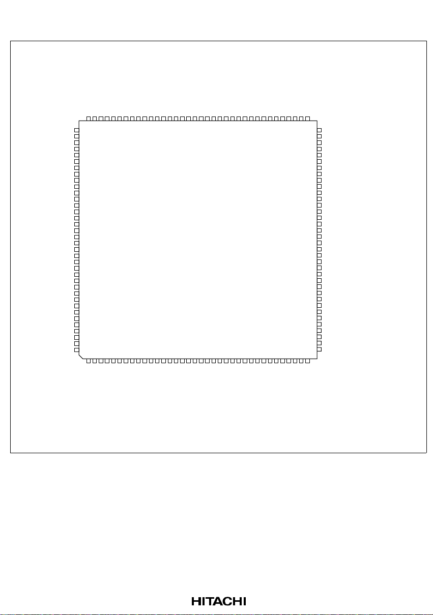
1.3 Pin Arrangement
P51/RxD2/IRQ1
P50/TxD2/IRQ0
PH1/CS5
PH0/CS4
PG3/CS3
PG2/CS2
PG1/CS1
PG0/CS0
STBY
108
107
106
105
104
103
102
101
VCC
PC0/A0
PC1/A1
100
PC2/A2
PC3/A3
P52/SCK2/IRQ2
P53/ADTRG/IRQ3
PH2/CS6/(IRQ6)
PH3/CS7/OE/(IRQ7)
PG4/BREQO
PG5/BACK
PG6/BREQ
VCC
P40/AN0
P41/AN1
P42/AN2
P43/AN3
Vref
AVCC
P44/AN4
P45/AN5
P46/AN6/DA0
P47/AN7/DA1
P54/AN12/IRQ4
P55/AN13/IRQ5
P56/AN14/DA2/IRQ6
P57/AN15/DA3/IRQ7
P80/EDREQ2/(IRQ0)
P81/EDREQ3/(IRQ1)
P82/ETEND2/(IRQ2)
AVSS
NC
P35/SCK1/(OE)
P34/SCK0
P33/RxD1
P32/RxD0/IrRxD
VSS
P31/TxD1
P30/TxD0/IrTxD
MD0
MD1
109
110
111
112
113
114
115
116
117
118
119
120
121
122
123
124
125
126
127
128
129
130
131
*2
132
133
134
135
136
137
138
139
140
141
142
143
144
1234567891011121314151617181920212223242526272829303132333435
MD2
VSS
XTAL
EXTAL
VCC
PF7/ø
PLLVCC
RES
PLLVSS
PF6/AS
PF5/RD
PF4/HWR
PF3/LWR
PF2/LCAS/IRQ15
PF1/UCAS/IRQ14
PF0/WAIT
P65/TMO1/DACK1/IRQ13
P64/TMO0/DACK0/IRQ12
P63/TMCI1/TEND1/IRQ11
P62/TMCI0/TEND0/IRQ10
PD0/D8
PD1/D9
PD2/D10
PD3/D11
VSS
PD4/D12
PD5/D13
999897969594939291908988878685848382818079787776757473
Pin Arrangement
(FP-144)
PC4/A4
PC5/A5
VSS
PC6/A6
PC7/A7
PB0/A8
PB1/A9
VSS
PB2/A10
PB3/A11
PB4/A12
PB5/A13
PB6/A14
PB7/A15
PA0/A16
PA1/A17
VSS
PA2/A18
PA3/A19
PA4/A20
PA5/A21
PA6/A22
NC
PA7/A23
PD6/D14
PD7/D15
72
PE0/D0
71
PE1/D1
70
PE2/D2
69
PE3/D3
68
VCC
67
PE4/D4
66
PE5/D5
65
PE6/D6
64
PE7/D7
63
*1
FWE
62
P61/TMRI1/DREQ1/IRQ9
61
P60/TMRI0/DREQ0/IRQ8
60
P27/PO7/TIOCB5/EDRAK1/(IRQ15)
59
P26/PO6/TIOCA5/EDRAK0/(IRQ14)
58
P25/PO5/TIOCB4/(IRQ13)
57
P24/PO4/TIOCA4/(IRQ12)
56
P23/PO3/TIOCD3/(IRQ11)
55
P22/PO2/TIOCC3/(IRQ10)
54
P21/PO1/TIOCB3/(IRQ9)
53
P20/PO0/TIOCA3/(IRQ8)
52
P17/PO15/TIOCB2/TCLKD/EDRAK3
51
P16/PO14/TIOCA2/EDRAK2
50
P15/PO13/TIOCB1/TCLKC
49
P14/PO12/TIOCA1
48
VSS
47
P13/PO11/TIOCD0/TCLKB
46
P12/PO10/TIOCC0/TCLKA
45
P11/PO9/TIOCB0
44
P10/PO8/TIOCA0
43
P75/EDACK1/(DACK1)
42
P74/EDACK0/(DACK0)
41
P73/ETEND1/(TEND1)
40
VCC
39
NMI
38
WDTOVF
37
36
P83/ETEND3/(IRQ3)
P84/EDACK2/(IRQ4)
P85/EDACK3/(IRQ5)
Notes: 1. The FWE pin is used only in the F-ZTAT version. In other versions, this is an NC pin.
2. An NC pin should be either fixed to VSS or opened.
Figure 1.2 Pin Arrangement (FP-144: Top View)
P72/ETEND0/(TEND0)
P70/EDREQ0/(DREQ0)
P71/EDREQ1/(DREQ1)
7
Page 25

1.4 Pin Functions in Each Operating Mode
Table 1.2 Pin Functions in Each Operating Mode
Pin Name
Pin
No. Mode 1 Mode 2 Mode 4 Mode 5 Mode 6 Mode 7
1
MD2 MD2 MD2 MD2 MD2
2
P83/
ETEND3/
(IRQ3)
3
P84/
EDACK2/
(IRQ4)
4
P85/
EDACK3/
(IRQ5)
5
VCC VCC VCC VCC VCC
6
A0 A0 PC0/A0 A0 A0
7
A1 A1 PC1/A1 A1 A1
8
A2 A2 PC2/A2 A2 A2
9
A3 A3 PC3/A3 A3 A3
10
A4 A4 PC4/A4 A4 A4
P83/
ETEND3/
(IRQ3)
P84/
EDACK2/
(IRQ4)
P85/
EDACK3/
(IRQ5)
P83/
ETEND3/
(IRQ3)
P84/
EDACK2/
(IRQ4)
P85/
EDACK3/
(IRQ5)
P83/
ETEND3/
(IRQ3)
P84/
EDACK2/
(IRQ4)
P85/
EDACK3/
(IRQ5)
P83/
ETEND3/
(IRQ3)
P84/
EDACK2/
(IRQ4)
P85/
EDACK3/
(IRQ5)
MD2 VSS
When EXPE = 1:
P83/ETEND3/
(IRQ3)
When EXPE = 0:
P83/(IRQ3)
When EXPE = 1:
P84/EDACK2/
(IRQ4)
When EXPE = 0:
P84/(IRQ4)
When EXPE = 1:
P85/EDACK3/
(IRQ5)
When EXPE = 0:
P85/(IRQ5)
VCC VCC
When EXPE = 1:
PC0/A0
When EXPE = 0:
PC0
When EXPE = 1:
PC1/A1
When EXPE = 0:
PC1
When EXPE = 1:
PC2/A2
When EXPE = 0:
PC2
When EXPE = 1:
PC3/A3
When EXPE = 0:
PC3
When EXPE = 1:
PC4/A4
When EXPE = 0:
PC4
Flash
Memory
Programmer Mode
NC
NC
NC
A0
A1
A2
A3
A4
8
Page 26

Pin Name
Pin
No. Mode 1 Mode 2 Mode 4 Mode 5 Mode 6 Mode 7
11 A5 A5 PC5/A5 A5 A5 When EXPE = 1:
PC5/A5
When EXPE = 0:
PC5
12 VSS VSS VSS VSS VSS VSS VSS
13 A6 A6 PC6/A6 A6 A6 When EXPE = 1:
PC6/A6
When EXPE = 0:
PC6
14 A7 A7 PC7/A7 A7 A7 When EXPE = 1:
PC7/A7
When EXPE = 0:
PC7
15 A8 A8 PB0/A8 A8 A8 When EXPE = 1:
PB0/A8
When EXPE = 0:
PB0
16 A9 A9 PB1/A9 A9 A9 When EXPE = 1:
PB1/A9
When EXPE = 0:
PB1
17 A10 A10 PB2/A10 A10 A10 When EXPE = 1:
PB2/A10
When EXPE = 0:
PB2
18 A11 A11 PB3/A11 A11 A11 When EXPE = 1:
PB3/A11
When EXPE = 0:
PB3
19 VSS VSS VSS VSS VSS VSS VSS
20 A12 A12 PB4/A12 A12 A12 When EXPE = 1:
PB4/A12
When EXPE = 0:
PB4
21 A13 A13 PB5/A13 A13 A13 When EXPE = 1:
PB5/A13
When EXPE = 0:
PB5
Flash
Memory
Programmer Mode
A5
A6
A7
A8
A9
A10
A11
A12
A13
9
Page 27

Pin Name
Pin
No. Mode 1 Mode 2 Mode 4 Mode 5 Mode 6 Mode 7
22 A14 A14 PB6/A14 A14 A14 When EXPE = 1:
PB6/A14
When EXPE = 0:
PB6
23 A15 A15 PB7/A15 A15 A15 When EXPE = 1:
PB7/A15
When EXPE = 0:
PB7
24 A16 A16 PA0/A16 A16 A16 When EXPE = 1:
PA0/A16
When EXPE = 0:
PA0
25 A17 A17 PA1/A17 A17 A17 When EXPE = 1:
PA1/A17
When EXPE = 0:
PA1
26 VSS VSS VSS VSS VSS VSS VSS
27 A18 A18 PA2/A18 A18 A18 When EXPE = 1:
PA2/A18
When EXPE = 0:
PA2
28 A19 A19 PA3/A19 A19 A19 When EXPE = 1:
PA3/A19
When EXPE = 0:
PA3
29 A20 A20 PA4/A20 A20 A20 When EXPE = 1:
PA4/A20
When EXPE = 0:
PA4
30 PA5/A21 PA5/A21 PA5/A21 PA5/A21 PA5/A21 When EXPE = 1:
PA5/A21
When EXPE = 0:
PA5
31 PA6/A22 PA6/A22 PA6/A22 PA6/A22 PA6/A22 When EXPE = 1:
PA6/A22
When EXPE = 0:
PA6
Flash
Memory
Programmer Mode
A14
A15
A16
A17
A18
NC
NC
NC
NC
10
Page 28

Pin Name
Pin
No. Mode 1 Mode 2 Mode 4 Mode 5 Mode 6 Mode 7
32 PA7/A23 PA7/A23 PA7/A23 PA7/A23 PA7/A23 When EXPE = 1:
PA7/A23
When EXPE = 0:
PA7
33 NC NC NC NC NC NC NC
34 P70/
EDREQ0/
(DREQ0)
35 P71/
EDREQ1/
(DREQ1)
36 P72/
ETEND0/
(TEND0)
37 WDTOVF WDTOVF WDTOVF WDTOVF WDTOVF WDTOVF NC
38 NMI NMI NMI NMI NMI NMI VCC
39 VCC VCC VCC VCC VCC VCC VCC
40 P73/
ETEND1/
(TEND1)
41 P74/
EDACK0/
(DACK0)
42 P75/
EDACK1/
(DACK1)
43 P10/PO8/
TIOCA0
P70/
EDREQ0/
(DREQ0)
P71/
EDREQ1/
(DREQ1)
P72/
ETEND0/
(TEND0)
P73/
ETEND1/
(TEND1)
P74/
EDACK0/
(DACK0)
P75/
EDACK1/
(DACK1)
P10/PO8/
TIOCA0
P70/
EDREQ0/
(DREQ0)
P71/
EDREQ1/
(DREQ1)
P72/
ETEND0/
(TEND0)
P73/
ETEND1/
(TEND1)
P74/
EDACK0/
(DACK0)
P75/
EDACK1/
(DACK1)
P10/PO8/
TIOCA0
P70/
EDREQ0/
(DREQ0)
P71/
EDREQ1/
(DREQ1)
P72/
ETEND0/
(TEND0)
P73/
ETEND1/
(TEND1)
P74/
EDACK0/
(DACK0)
P75/
EDACK1/
(DACK1)
P10/PO8/
TIOCA0
P70/
EDREQ0/
(DREQ0)
P71/
EDREQ1/
(DREQ1)
P72/
ETEND0/
(TEND0)
P73/
ETEND1/
(TEND1)
P74/
EDACK0/
(DACK0)
P75/
EDACK1/
(DACK1)
P10/PO8/
TIOCA0
When EXPE = 1:
P70/EDREQ0/
(DREQ0)
When EXPE = 0:
P70/(DREQ0)
When EXPE = 1:
P71/EDREQ1/
(DREQ1)
When EXPE = 0:
P71/(DREQ1)
When EXPE = 1:
P72/ETEND0/
(TEND0)
When EXPE = 0:
P72/(TEND0)
When EXPE = 1:
P73/ETEND1/
(TEND1)
When EXPE = 0:
P73/(TEND1)
When EXPE = 1:
P74/EDACK0/
(DACK0)
When EXPE = 0:
P74/(DACK0)
When EXPE = 1:
P75/EDACK1/
(DACK1)
When EXPE = 0:
P75/(DACK1)
P10/PO8/
TIOCA0
Flash
Memory
Programmer Mode
NC
NC
NC
NC
NC
NC
NC
NC
11
Page 29

Pin Name
Pin
No. Mode 1 Mode 2 Mode 4 Mode 5 Mode 6 Mode 7
44 P11/PO9/
TIOCB0
45 P12/PO10/
TIOCC0/
TCLKA
46 P13/PO11/
TIOCD0/
TCLKB
47 VSS VSS VSS VSS VSS VSS VSS
48 P14/PO12/
TIOCA1
49 P15/PO13/
TIOCB1/
TCLKC
50 P16/PO14/
TIOCA2/
EDRAK2
51 P17/PO15/
TIOCB2/
TCLKD/
EDRAK3
52 P20/PO0/
TIOCA3/
(IRQ8)
53 P21/PO1/
TIOCB3/
(IRQ9)
54 P22/PO2/
TIOCC3/
(IRQ10)
55 P23/PO3/
TIOCD3/
(IRQ11)
P11/PO9/
TIOCB0
P12/PO10/
TIOCC0/
TCLKA
P13/PO11/
TIOCD0/
TCLKB
P14/PO12/
TIOCA1
P15/PO13/
TIOCB1/
TCLKC
P16/PO14/
TIOCA2/
EDRAK2
P17/PO15/
TIOCB2/
TCLKD/
EDRAK3
P20/PO0/
TIOCA3/
(IRQ8)
P21/PO1/
TIOCB3/
(IRQ9)
P22/PO2/
TIOCC3/
(IRQ10)
P23/PO3/
TIOCD3/
(IRQ11)
P11/PO9/
TIOCB0
P12/PO10/
TIOCC0/
TCLKA
P13/PO11/
TIOCD0/
TCLKB
P14/PO12/
TIOCA1
P15/PO13/
TIOCB1/
TCLKC
P16/PO14/
TIOCA2/
EDRAK2
P17/PO15/
TIOCB2/
TCLKD/
EDRAK3
P20/PO0/
TIOCA3/
(IRQ8)
P21/PO1/
TIOCB3/
(IRQ9)
P22/PO2/
TIOCC3/
(IRQ10)
P23/PO3/
TIOCD3/
(IRQ11)
P11/PO9/
TIOCB0
P12/PO10/
TIOCC0/
TCLKA
P13/PO11/
TIOCD0/
TCLKB
P14/PO12/
TIOCA1
P15/PO13/
TIOCB1/
TCLKC
P16/PO14/
TIOCA2/
EDRAK2
P17/PO15/
TIOCB2/
TCLKD/
EDRAK3
P20/PO0/
TIOCA3/
(IRQ8)
P21/PO1/
TIOCB3/
(IRQ9)
P22/PO2/
TIOCC3/
(IRQ10)
P23/PO3/
TIOCD3/
(IRQ11)
P11/PO9/
TIOCB0
P12/PO10/
TIOCC0/
TCLKA
P13/PO11/
TIOCD0/
TCLKB
P14/PO12/
TIOCA1
P15/PO13/
TIOCB1/
TCLKC
P16/PO14/
TIOCA2/
EDRAK2
P17/PO15/
TIOCB2/
TCLKD/
EDRAK3
P20/PO0/
TIOCA3/
(IRQ8)
P21/PO1/
TIOCB3/
(IRQ9)
P22/PO2/
TIOCC3/
(IRQ10)
P23/PO3/
TIOCD3/
(IRQ11)
P11/PO9/
TIOCB0
P12/PO10/
TIOCC0/
TCLKA
P13/PO11/
TIOCD0/
TCLKB
P14/PO12/
TIOCA1
P15/PO13/
TIOCB1/
TCLKC
When EXPE = 1:
P16/PO14/
TIOCA2/
EDRAK2
When EXPE = 0:
P16/PO14/
TIOCA2
When EXPE = 1:
P17/PO15/
TIOCB2/TCLKD/E
DRAK3
When EXPE = 0:
P17/PO15/
TIOCB2/TCLKD
P20/PO0/
TIOCA3/
(IRQ8)
P21/PO1/
TIOCB3/
(IRQ9)
P22/PO2/
TIOCC3/
(IRQ10)
P23/PO3/
TIOCD3/
(IRQ11)
Flash
Memory
Programmer Mode
NC
NC
NC
NC
NC
NC
NC
NC
NC
OE
CE
12
Page 30

Pin Name
Pin
No. Mode 1 Mode 2 Mode 4 Mode 5 Mode 6 Mode 7
56 P24/PO4/
TIOCA4/
(IRQ12)
57 P25/PO5/
TIOCB4/
(IRQ13)
58 P26/PO6/
TIOCA5/
EDRAK0/
(IRQ14)
59 P27/PO7/
TIOCB5/
EDRAK1/
(IRQ15)
60 P60/TMRI0/
DREQ0/
IRQ8
61 P61/TMRI1/
DREQ1/
IRQ9
62 FWE* FWE* FWE* FWE* FWE* FWE* FWE*
63 D7 PE7/D7 PE7/D7 D7 PE7/D7 When EXPE = 1:
64 D6 PE6/D6 PE6/D6 D6 PE6/D6 When EXPE = 1:
65 D5 PE5/D5 PE5/D5 D5 PE5/D5 When EXPE = 1:
P24/PO4/
TIOCA4/
(IRQ12)
P25/PO5/
TIOCB4/
(IRQ13)
P26/PO6/
TIOCA5/
EDRAK0/
(IRQ14)
P27/PO7/
TIOCB5/
EDRAK1/
(IRQ15)
P60/TMRI0/
DREQ0/
IRQ8
P61/TMRI1/
DREQ1/
IRQ9
P24/PO4/
TIOCA4/
(IRQ12)
P25/PO5/
TIOCB4/
(IRQ13)
P26/PO6/
TIOCA5/
EDRAK0/
(IRQ14)
P27/PO7/
TIOCB5/
EDRAK1/
(IRQ15)
P60/TMRI0/
DREQ0/
IRQ8
P61/TMRI1/
DREQ1/
IRQ9
P24/PO4/
TIOCA4/
(IRQ12)
P25/PO5/
TIOCB4/
(IRQ13)
P26/PO6/
TIOCA5/
EDRAK0/
(IRQ14)
P27/PO7/
TIOCB5/
EDRAK1/
(IRQ15)
P60/TMRI0/
DREQ0/
IRQ8
P61/TMRI1/
DREQ1/
IRQ9
P24/PO4/
TIOCA4/
(IRQ12)
P25/PO5/
TIOCB4/
(IRQ13)
P26/PO6/
TIOCA5/
EDRAK0/
(IRQ14)
P27/PO7/
TIOCB5/
EDRAK1/
(IRQ15)
P60/TMRI0/
DREQ0/
IRQ8
P61/TMRI1/
DREQ1/
IRQ9
P24/PO4/
TIOCA4/
(IRQ12)
P25/PO5/
TIOCB4/
(IRQ13)
When EXPE = 1:
P26/PO6/
TIOCA5/
EDRAK0/
(IRQ14)
When EXPE = 0:
P26/PO6/
TIOCA5/(IRQ14)
When EXPE = 1:
P27/PO7/
TIOCB5/
EDRAK1/
(IRQ15)
When EXPE = 0:
P27/PO7/
TIOCB5/(IRQ15)
P60/TMRI0/
DREQ0/
IRQ8
P61/TMRI1/
DREQ1/
IRQ9
PE7/D7
When EXPE = 0:
PE7
PE6/D6
When EXPE = 0:
PE6
PE5/D5
When EXPE = 0:
PE5
Flash
Memory
Programmer Mode
WE
VSS
NC
NC
NC
NC
NC
NC
NC
13
Page 31

Pin Name
Pin
No. Mode 1 Mode 2 Mode 4 Mode 5 Mode 6 Mode 7
66 D4 PE4/D4 PE4/D4 D4 PE4/D4 When EXPE = 1:
PE4/D4
When EXPE = 0:
PE4
67 VCC VCC VCC VCC VCC VCC VCC
68 D3 PE3/D3 PE3/D3 D3 PE3/D3 When EXPE = 1:
PE3/D3
When EXPE = 0:
PE3
69 D2 PE2/D2 PE2/D2 D2 PE2/D2 When EXPE = 1:
PE2/D2
When EXPE = 0:
PE2
70 D1 PE1/D1 PE1/D1 D1 PE1/D1 When EXPE = 1:
PE1/D1
When EXPE = 0:
PE1
71 D0 PE0/D0 PE0/D0 D0 PE0/D0 When EXPE = 1:
PE0/D0
When EXPE = 0:
PE0
72 D15 D15 D15 D15 D15 When EXPE = 1:
D15
When EXPE = 0:
PD7
73 D14 D14 D14 D14 D14 When EXPE = 1:
D14
When EXPE = 0:
PD6
74 D13 D13 D13 D13 D13 When EXPE = 1:
D13
When EXPE = 0:
PD5
75 D12 D12 D12 D12 D12 When EXPE = 1:
D12
When EXPE = 0:
PD4
76 VSS VSS VSS VSS VSS VSS VSS
Flash
Memory
Programmer Mode
NC
NC
NC
NC
NC
I/O7
I/O6
I/O5
I/O4
14
Page 32

Pin Name
Pin
No. Mode 1 Mode 2 Mode 4 Mode 5 Mode 6 Mode 7
77 D11 D11 D11 D11 D11 When EXPE = 1:
D11
When EXPE = 0:
PD3
78 D10 D10 D10 D10 D10 When EXPE = 1:
D10
When EXPE = 0:
PD2
79 D9 D9 D9 D9 D9 When EXPE = 1: D9
When EXPE = 0:
PD1
80 D8 D8 D8 D8 D8 When EXPE = 1: D8
When EXPE = 0:
PD0
81 P62/TMCI0/
TEND0/
IRQ10
82 P63/TMCI1/
TEND1/
IRQ11
83 P64/TMO0/
DACK0/
IRQ12
84 P65/TMO1/
DACK1/
IRQ13
85 PF0/WAIT PF0/WAIT PF0/WAIT PF0/WAIT PF0/WAIT When EXPE = 1:
86 PF1/UCAS/
IRQ14
P62/TMCI0/
TEND0/
IRQ10
P63/TMCI1/
TEND1/
IRQ11
P64/TMO0/
DACK0/
IRQ12
P65/TMO1/
DACK1/
IRQ13
PF1/UCAS/
IRQ14
P62/TMCI0/
TEND0/
IRQ10
P63/TMCI1/
TEND1/
IRQ11
P64/TMO0/
DACK0/
IRQ12
P65/TMO1/
DACK1/
IRQ13
PF1/UCAS/
IRQ14
P62/TMCI0/
TEND0/
IRQ10
P63/TMCI1/
TEND1/
IRQ11
P64/TMO0/
DACK0/
IRQ12
P65/TMO1/
DACK1/
IRQ13
PF1/UCAS/
IRQ14
P62/TMCI0/
TEND0/
IRQ10
P63/TMCI1/
TEND1/
IRQ11
P64/TMO0/
DACK0/
IRQ12
P65/TMO1/
DACK1/
IRQ13
PF1/UCAS/
IRQ14
P62/TMCI0/
TEND0/
IRQ10
P63/TMCI1/
TEND1/
IRQ11
P64/TMO0/
DACK0/
IRQ12
P65/TMO1/
DACK1/
IRQ13
PF0/WAIT
When EXPE = 0:
PF0
When EXPE = 1:
PF1/UCAS/
IRQ14
When EXPE = 0:
PF1/IRQ14
Flash
Memory
Programmer Mode
I/O3
I/O2
I/O1
I/O0
NC
NC
NC
NC
NC
NC
15
Page 33

Pin Name
Pin
No. Mode 1 Mode 2 Mode 4 Mode 5 Mode 6 Mode 7
87 PF2/LCAS/
IRQ15
88 PF3/LWR PF3/LWR PF3/LWR PF3/LWR PF3/LWR When EXPE = 1:
89 HWR HWR HWR HWR HWR When EXPE = 1:
90 RD RD RD RD RD When EXPE = 1: RD
91 PF6/AS PF6/AS PF6/AS PF6/AS PF6/AS When EXPE = 1:
92 PLLVSS PLLVSS PLLVSS PLLVSS PLLVSS PLLVSS VSS
93 RES RES RES RES RES RES RES
94 PLLVCC PLLVCC PLLVCC PLLVCC PLLVCC PLLVCC VCC
95 PF7/ø PF7/ø PF7/ø PF7/ø PF7/ø PF7/ø NC
96 VCC VCC VCC VCC VCC VCC VCC
97 EXTAL EXTAL EXTAL EXTAL EXTAL EXTAL EXTAL
98 XTAL XTAL XTAL XTAL XTAL XTAL XTAL
99 VSS VSS VSS VSS VSS VSS VSS
100 STBY STBY STBY STBY STBY STBY VCC
101 PG0/CS0 PG0/CS0 PG0/CS0 PG0/CS0 PG0/CS0 When EXPE = 1:
102 PG1/CS1 PG1/CS1 PG1/CS1 PG1/CS1 PG1/CS1 When EXPE = 1:
PF2/LCAS/
IRQ15
PF2/LCAS/
IRQ15
PF2/LCAS/
IRQ15
PF2/LCAS/
IRQ15
When EXPE = 1:
PF2/LCAS/
IRQ15
When EXPE = 0:
PF2/IRQ15
PF3/LWR
When EXPE = 0:
PF3
HWR
When EXPE = 0:
PF4
When EXPE = 0:
PF5
PF6/AS
When EXPE = 0:
PF6
PG0/CS0
When EXPE = 0:
PG0
PG1/CS1
When EXPE = 0:
PG1
Flash
Memory
Programmer Mode
NC
NC
NC
NC
NC
NC
NC
16
Page 34

Pin Name
Pin
No. Mode 1 Mode 2 Mode 4 Mode 5 Mode 6 Mode 7
103 PG2/CS2 PG2/CS2 PG2/CS2 PG2/CS2 PG2/CS2 When EXPE = 1:
PG2/CS2
When EXPE = 0:
PG2
104 PG3/CS3 PG3/CS3 PG3/CS3 PG3/CS3 PG3/CS3 When EXPE = 1:
PG3/CS3
When EXPE = 0:
PG3
105 PH0/CS4 PH0/CS4 PH0/CS4 PH0/CS4 PH0/CS4 When EXPE = 1:
PH0/CS4
When EXPE = 0:
PH0
106 PH1/CS5 PH1/CS5 PH1/CS5 PH1/CS5 PH1/CS5 When EXPE = 1:
PH1/CS5
When EXPE = 0:
PH1
107 P50/TxD2/
IRQ0
108 P51/RxD2/
IRQ1
109 P52/SCK2/
IRQ2
110 P53/
ADTRG/
IRQ3
111 PH2/CS6/
(IRQ6)
112 PH3/CS7/
OE/(IRQ7 )
113 PG4/
BREQO
P50/TxD2/
IRQ0
P51/RxD2/
IRQ1
P52/SCK2/
IRQ2
P53/
ADTRG/
IRQ3
PH2/CS6/
(IRQ6)
PH3/CS7/
OE/(IRQ7 )
PG4/
BREQO
P50/TxD2/
IRQ0
P51/RxD2/
IRQ1
P52/SCK2/
IRQ2
P53/
ADTRG/
IRQ3
PH2/CS6/
(IRQ6)
PH3/CS7/
OE/(IRQ7 )
PG4/
BREQO
P50/TxD2/
IRQ0
P51/RxD2/
IRQ1
P52/SCK2/
IRQ2
P53/
ADTRG/
IRQ3
PH2/CS6/
(IRQ6)
PH3/CS7/
OE/(IRQ7 )
PG4/
BREQO
P50/TxD2/
IRQ0
P51/RxD2/
IRQ1
P52/SCK2/
IRQ2
P53/ADTRG/
IRQ3
PH2/CS6/
(IRQ6)
PH3/CS7/
OE/(IRQ7 )
PG4/BREQO When EXPE = 1:
P50/TxD2/
IRQ0
P51/RxD2/
IRQ1
P52/SCK2/
IRQ2
P53/ADTRG/
IRQ3
When EXPE = 1:
PH2/CS6/(IRQ6)
When EXPE = 0:
PH2/(IRQ6)
When EXPE = 1:
PH3/CS7/OE/
(IRQ7)
When EXPE = 0:
PH3/(IRQ7)
PG4/BREQO
When EXPE = 0:
PG4
Flash
Memory
Programmer Mode
NC
NC
NC
NC
VSS
VSS
VCC
NC
NC
NC
NC
17
Page 35

Pin Name
Pin
No. Mode 1 Mode 2 Mode 4 Mode 5 Mode 6 Mode 7
114 PG5/BACK PG5/BACK PG5/BACK PG5/BACK PG5/BACK When EXPE = 1:
PG5/BACK
When EXPE = 0:
PG5
115 PG6/BREQ PG6/BREQ PG6/BREQ PG6/BREQ PG6/BREQ When EXPE = 1:
PG6/BREQ
When EXPE = 0:
PG6
116 VCC VCC VCC VCC VCC VCC VCC
117 P40/AN0 P40/AN0 P40/AN0 P40/AN0 P40/AN0 P40/AN0 NC
118 P41/AN1 P41/AN1 P41/AN1 P41/AN1 P41/AN1 P41/AN1 NC
119 P42/AN2 P42/AN2 P42/AN2 P42/AN2 P42/AN2 P42/AN2 NC
120 P43/AN3 P43/AN3 P43/AN3 P43/AN3 P43/AN3 P43/AN3 NC
121 Vref Vref Vref Vref Vref Vref NC
122 AVCC AVCC AVCC AVCC AVCC AVCC VCC
123 P44/AN4 P44/AN4 P44/AN4 P44/AN4 P44/AN4 P44/AN4 NC
124 P45/AN5 P45/AN5 P45/AN5 P45/AN5 P45/AN5 P45/AN5 NC
125 P46/
AN6/DA0
126 P47/AN7/
DA1
127 P54/AN12/
IRQ4
128 P55/AN13/
IRQ5
129 P56/AN14/
DA2/IRQ6
130 P57/AN15/
DA3/IRQ7
131 AVSS AVSS AVSS AVSS AVSS AVSS VSS
132 NC NC NC NC NC NC NC
133 P35/SCK1/
(OE)
134 P34/SCK0 P34/SCK0 P34/SCK0 P34/SCK0 P34/SCK0 P34/SCK0 NC
135 P33/RxD1 P33/RxD1 P33/RxD1 P33/RxD1 P33/RxD1 P33/RxD1 NC
136 VSS VSS VSS VSS VSS VSS VSS
P46/
AN6/DA0
P47/AN7/
DA1
P54/AN12/
IRQ4
P55/AN13/
IRQ5
P56/AN14/
DA2/IRQ6
P57/AN15/
DA3/IRQ7
P35/SCK1/
(OE)
P46/
AN6/DA0
P47/AN7/
DA1
P54/AN12/
IRQ4
P55/AN13/
IRQ5
P56/AN14/
DA2/IRQ6
P57/AN15/
DA3/IRQ7
P35/SCK1/
(OE)
P46/
AN6/DA0
P47/AN7/
DA1
P54/AN12/
IRQ4
P55/AN13/
IRQ5
P56/AN14/
DA2/IRQ6
P57/AN15/
DA3/IRQ7
P35/SCK1/
(OE)
P46/AN6/DA0 P46/AN6/DA0 NC
P47/AN7/DA1 P47/AN7/DA1 NC
P54/AN12/
IRQ4
P55/AN13/
IRQ5
P56/AN14/
DA2/IRQ6
P57/AN15/
DA3/IRQ7
P35/SCK1/
(OE)
P54/AN12/
IRQ4
P55/AN13/
IRQ5
P56/AN14/
DA2/IRQ6
P57/AN15/
DA3/IRQ7
When EXPE = 1:
P35/SCK1/(OE)
When EXPE = 0:
P35/SCK1
Flash
Memory
Programmer Mode
NC
NC
NC
NC
NC
NC
NC
18
Page 36

Pin Name
Pin
No. Mode 1 Mode 2 Mode 4 Mode 5 Mode 6 Mode 7
137 P32/RxD0/
IrRxD
138 P31/TxD1 P31/TxD1 P31/TxD1 P31/TxD1 P31/TxD1 P31/TxD1 NC
139 P30/TxD0/
IrTxD
140 P80/
EDREQ2/
(IRQ0)
141 P81/
EDREQ3/
(IRQ1)
142 P82/
ETEND2/
(IRQ2)
143 MD0 MD0 MD0 MD0 MD0 MD0 VSS
144 MD1 MD1 MD1 MD1 MD1 MD1 VSS
P32/RxD0/
IrRxD
P30/TxD0/
IrTxD
P80/
EDREQ2/
(IRQ0)
P81/
EDREQ3/
(IRQ1)
P82/
ETEND2/
(IRQ2)
P32/RxD0/
IrRxD
P30/TxD0/
IrTxD
P80/
EDREQ2/
(IRQ0)
P81/
EDREQ3/
(IRQ1)
P82/
ETEND2/
(IRQ2)
P32/RxD0/
IrRxD
P30/TxD0/
IrTxD
P80/
EDREQ2/
(IRQ0)
P81/
EDREQ3/
(IRQ1)
P82/
ETEND2/
(IRQ2)
P32/RxD0/
IrRxD
P30/TxD0/
IrTxD
P80/
EDREQ2/
(IRQ0)
P81/
EDREQ3/
(IRQ1)
P82/
ETEND2/
(IRQ2)
P32/RxD0/
IrRxD
P30/TxD0/
IrTxD
When EXPE = 1:
P80/EDREQ2/
(IRQ0)
When EXPE = 0:
P80/(IRQ0)
When EXPE = 1:
P81/EDREQ3/
(IRQ1)
When EXPE = 0:
P81/(IRQ1)
When EXPE = 1:
P82/ETEND2/
(IRQ2)
When EXPE = 0:
P82/(IRQ2)
Flash
Memory
Programmer Mode
VCC
NC
NC
NC
NC
Note: *F-ZTAT version only. In other versions, this is an NC pin.
19
Page 37

1.5 Pin Functions
Table 1.3 Pin Functions
Pin No.
Type Symbol FP-144 I/O Name and Function
Power VCC 5, 39, 67,
96, 116
VSS 12, 19, 26,
47, 76, 99,
136
PLLVCC 94 Input PLL power: The on-chip PLL oscillator
PLLVSS 92 Input PLL ground: The on-chip PLL oscillator
Clock XTAL 98 Input For connection to a crystal oscillator.
EXTAL 97 Input For connection to a crystal oscillator.
ø 95 Output System clock: Supplies the system
Input Power: For connection to the power
supply. All V
pins should be connected
CC
to the system power supply.
Input Ground: For connection to the power
supply. All V
pins should be connected
SS
to the system power supply (0 V).
power supply.
ground.
See section 19, Clock Pulse Generator,
in the H8S/2678 Series Hardware
Manual for typical connection diagrams
for a crystal oscillator and external clock
input.
The EXTAL pin can also input an
external clock. See section 19, Clock
Pulse Generator, in the H8S/2678
Series Hardware Manual for typical
connection diagrams for a crystal
oscillator and external clock input.
clock to external devices.
20
Page 38

Pin No.
Type Symbol FP-144 I/O Name and Function
Operating mode
control
MD2 to MD0 1, 144, 143 Input Mode pins: These pins set the
operating mode. The relation between
the settings of pins MD2 to MD0 and the
operating mode is shown below. These
pins should not be changed while the
MCU is operating.
MD0 MD1 MD0 Operating Mode
000 —
1 Mode 1
1 0 Mode 2
1 —
1 0 0 Mode 4
1 Mode 5
1 0 Mode 6
1 Mode 7
System control RES 93 Input Reset input: When this pin is driven
low, the chip is reset.
STBY 100 Input Standby: When this pin is driven low, a
transition is made to hardware standby
mode.
BREQ 115 Input Bus request: Requests chip to release
the bus to an external bus master.
BREQO 113 Output Bus request output: External bus
request signal used when an internal
bus master accesses external space
when the external bus is released.
BACK 114 Output Bus request acknowledge: Indicates
that the bus has been released to an
external bus master.
FWE* 62 Input Flash write enable: Enables/disables
flash memory.
21
Page 39

Pin No.
Type Symbol FP-144 I/O Name and Function
Interrupt signals NMI 38 Input Nonmaskable interrupt: Requests a
nonmaskable interrupt. Fix high when
not used.
IRQ15 to
IRQ0
(IRQ15) to
(IRQ0)
Address bus A23 to A0 32 to 27,
Data bus D15 to D0 72 to 75,
Bus control CS7 to CS0 112, 111,
AS 91 Output Address strobe: When this pin is low, it
RD 90 Output Read: When this pin is low, it indicates
HWR 89 Output High write/write enable: Strobe signal
LWR 88 Output Low write: Strobe signal indicating that
87, 86,
84 to 81,
61, 60,
130 to 127,
110 to 107,
59 to 52,
112, 111,
4 to 2,
142 to 140
25 to 20,
18 to 13,
11 to 6
77 to 80,
63 to 66,
68 to 71
106 to 101
Input Interrupt request 15 to 0: These pins
request a maskable interrupt.
Output Address bus: These pins output an
address.
Input/
output
Output Chip select: Signals that select areas 7
Data bus: These pins constitute a
bidirectional data bus.
to 0.
indicates that address output on the
address bus is valid.
that the external address space is being
read.
indicating that external space is to be
written, and the upper half (D15 to D8)
of the data bus is enabled.
Write enable signal for DRAM interface
space.
external space is to be written, and the
lower half (D7 to D0) of the data bus is
enabled.
22
Page 40

Pin No.
Type Symbol FP-144 I/O Name and Function
Bus control UCAS 86 Output Upper column address strobe: Upper
column address strobe signal for 16-bit
DRAM interface space.
Column address strobe signal for 8-bit
DRAM interface space.
LCAS 87 Output Lower column address strobe: Lower
column address strobe signal for 16-bit
DRAM interface space.
WAIT 85 Input Wait: Requests insertion of a wait state
in the bus cycle when accessing
external 3-state address space.
DMA controller
(DMAC)
EXDMA controller
(EXDMAC)
OE
(OE)
DREQ1,
DREQ0,
(DREQ1),
(DREQ0)
TEND1,
TEND0,
(TEND1),
(TEND0)
DACK1,
DACK0,
(DACK1),
(DACK0),
EDREQ3 to
EDREQ0
ETEND3 to
ETEND0
EDACK3 to
EDACK0
EDRAK3 to
EDRAK0
112
133
61
60
35
34
82
81
40
36
84
83
42
41
141, 140,
35, 34
2, 142, 40,36Output EXDMA transfer end 3 to 0: These
4, 3, 42, 41
51, 50, 59,
58 Output
Output Output enable: Output enable signal for
DRAM interface space.
Input DMA transfer request 1, 0: These
signals request DMAC activation.
Output DMA transfer end 1, 0: These signals
indicate the end of DMAC data transfer.
DMA transfer acknowledge 1, 0:
Output
Input EXDMA transfer request 3 to 0: These
Output
DMAC single address transfer
acknowledge signals.
signals request EXDMAC activation.
signals indicate the end of EXDMAC
data transfer.
EXDMA transfer acknowledge 3 to 0:
EXDMAC single address transfer
acknowledge signals.
EDREQ acknowledge 3 to 0: These
signals notify an external device of
acceptance and start of execution of an
external request.
23
Page 41

Pin No.
Type Symbol FP-144 I/O Name and Function
16-bit timer pulse
unit (TPU)
Programmable
pulse generator
(PPG)
8-bit timer TMO0,
TCLKD to
TCLKA
TIOCA0,
TIOCB0,
TIOCC0,
TIOCD0
TIOCA1,
TIOCB1
TIOCA2,
TIOCB2
TIOCA3,
TIOCB3,
TIOCC3,
TIOCD3
TIOCA4,
TIOCB4
TIOCA5,
TIOCB5
PO15 to
PO0
TMO1
TMCI0,
TMCI1
TMRI0,
TMRI1
51, 49, 46,
45 Input
43 to 46 Input/
output
48, 49 Input/
output
50, 51 Input/
output
52 to 55 Input/
output
56, 57 Input/
output
58, 59 Input/
output
51 to 48,
46 to 43,
59 to 52
83, 84 Output Compare match output: Compare
81, 82 Input Counter external clock input: Input
60, 61 Input Counter external reset input: Counter
Output Pulse output 15 to 0: Pulse output
Clock input D to A: External clock input
pins.
Input capture/output compare match
A0 to D0: TGR0A to TGR0D input
capture input/output compare
output/PWM output pins.
Input capture/output compare match
A1, B1: TGR1A and TGR1B input
capture input/output compare
output/PWM output pins.
Input capture/output compare match
A2, B2: TGR2A and TGR2B input
capture input/output compare
output/PWM output pins.
Input capture/output compare match
A3 to D3: TGR3A to TGR3D input
capture input/output compare
output/PWM output pins.
Input capture/output compare match
A4, B4: TGR4A and TGR4B input
capture input/output compare
output/PWM output pins.
Input capture/output compare match
A5, B5: TGR5A and TGR5B input
capture input/output compare
output/PWM output pins.
pins.
match output pins.
pins for the external clock input to the
counter.
reset input pins.
24
Page 42

Pin No.
Type Symbol FP-144 I/O Name and Function
Watchdog timer
(WDT)
Serial communication interface
(SCI)/smart card
interface (SCI0
with IrDA function)
A/D converter AN15 to
D/A converter DA3, DA2,
A/D converter,
D/A converter
WDTOVF 37 Output Watchdog timer overflow: Counter
overflow signal output pin in watchdog
timer mode.
TxD2, TxD1,
TxD0/IrTxD
RxD2, RxD1,
RxD0/IrRxD
SCK2, SCK1,
SCK0
AN12,
AN7 to AN0
ADTRG 110 Input A/D conversion external trigger input:
DA1, DA0
AVCC 122 Input The power supply pin for the A/D
AVSS 131 Input The ground pin for the A/D converter
Vref 121 Input The reference voltage input pin for the
107, 138,
139
108, 135,
137
109, 133,
134
130 to 127,
126 to 123,
120 to 117
130, 129,
126, 125
Output Transmit data (channels 0, 1, 2): Data
output pins.
Input Receive data (channels 0, 1, 2): Data
input pins.
Input/
output
Input Analog 15 to 12, 7 to 0: Analog input
Output Analog output: D/A converter analog
Serial clock (channels 0, 1, 2): Clock
input/output pins.
pins.
Pin for input of an external trigger to
start A/D conversion.
output pins.
converter and D/A converter.
When the A/D converter and D/A
converter are not used, this pin should
be connected to the system power
supply (+3 V).
and D/A converter.
This pin should be connected to the
system power supply (0 V).
A/D converter and D/A converter.
When the A/D converter and D/A
converter are not used, this pin should
be connected to the system power
supply (+3 V).
25
Page 43

Pin No.
Type Symbol FP-144 I/O Name and Function
I/O ports P17 to P10 51 to 48,
46 to 43
P27 to P20 59 to 52 Input/
P35 to P30 133 to 135,
137 to 139
P47 to P40 126 to 123,
120 to 117
P57 to P50 130 to 127,
110 to 107
P65 to P60 84 to 81,
61, 60
P75 to P70 42 to 40,
36 to 34
P85 to P80 4 to 2,
142 to 140
PA7 to PA0 32 to 27,
25, 24
PB7 to PB0 23 to 20,
18 to 15
Input/
output
output
Input/
output
Input Port 4: Eight input pins.
Input
Input/
output
Input/
output
Input/
output
Input/
output
Input/
output
Input/
output
Port 1: Eight input/output pins. The
direction of each pin can be selected in
the port 1 data direction register
(P1DDR).
Port 2: Eight input/output pins. The
direction of each pin can be selected in
the port 2 data direction register
(P2DDR).
Port 3: Six input/output pins. The
direction of each pin can be selected in
the port 3 data direction register
(P3DDR).
Port 5: Four input pins and four
input/output pins. The direction of each
input/output pin can be selected in the
port 5 data direction register (P5DDR).
Port 6: Six input/output pins. The
direction of each pin can be selected in
the port 6 data direction register
(P6DDR).
Port 7: Six input/output pins. The
direction of each pin can be selected in
the port 7 data direction register
(P7DDR).
Port 8: Six input/output pins. The
direction of each pin can be selected in
the port 8 data direction register
(P8DDR).
Port A: Eight input/output pins. The
direction of each pin can be selected in
the port A data direction register
(PADDR).
Port B: Eight input/output pins. The
direction of each pin can be selected in
the port B data direction register
(PBDDR).
26
Page 44

Pin No.
Type Symbol FP-144 I/O Name and Function
I/O ports PC7 to PC0 14, 13,
11 to 6
PD7 to PD0 72 to 75,
77 to 80
PE7 to PE0 63 to 66,
68 to 71
PF7 to PF0 95,
91 to 85
PG6 to PG0 115 to 113,
104 to 101
PH3 to PH0 112, 111,
106, 105
Note: * F-ZTAT version only. In other versions, this is an NC pin.
Input/
output
Input/
output
Input/
output
Input/
output
Input/
output
Input/
output
Port C: Eight input/output pins. The
direction of each pin can be selected in
the port C data direction register
(PCDDR).
Port D: Eight input/output pins. The
direction of each pin can be selected in
the port D data direction register
(PDDDR).
Port E: Eight input/output pins. The
direction of each pin can be selected in
the port E data direction register
(PEDDR).
Port F: Eight input/output pins. The
direction of each pin can be selected in
the port F data direction register
(PFDDR).
Port G: Seven input/output pins. The
direction of each pin can be selected in
the port G data direction register
(PGDDR).
Port H: Four input/output pins. The
direction of each pin can be selected in
the port H data direction register
(PHDDR).
27
Page 45

1.6 Product Lineup
Table 1.4 H8S/2678 Series Product Lineup
Package
Product Type Model Marking
2
H8S/2677*
F-ZTAT™ version HD64F2677 HD64F2677VFC 144-pin plastic QFP (FP-144)
H8S/2676*1F-ZTAT™ version HD64F2676 HD64F2676VFC 144-pin plastic QFP (FP-144)
Mask ROM version HD6432676 HD6432676FC
H8S/2675*2Mask ROM version HD6432675 HD6432675FC 144-pin plastic QFP (FP-144)
H8S/2673*1Mask ROM version HD6432673 HD6432673FC 144-pin plastic QFP (FP-144)
H8S/2670*1ROMless version HD6412670 HD6412670VFC 144-pin plastic QFP (FP-144)
Notes: 1. Under development
2. In planning stage
(Hitachi Package Code)
1.7 Package Dimensions
22.0 ± 0.2
20
108
109
22.0 ± 0.2
144
0.22 ± 0.05
*
0.20 ± 0.04
*Dimension including the plating thickness
1
0.10
0.10
Base material dimension
M
Figure 1.3 FP-144 Package Dimensions
73
36
72
37
2.70
+0.15
–0.10
0.10
0.5
3.05 Max
0.17 ± 0.05
0.15 ± 0.04
*
Hitachi Code
JEDEC
EIAJ
Weight
1.25
(reference value)
Unit: mm
1.0
0° – 8°
0.5 ± 0.1
FP-144G
—
Conforms
2.4 g
28
Page 46

Section 2 MCU Operating Modes
2.1 Overview
2.1.1 Operating Mode Selection (F-ZTAT Version)
The H8S/2678 Series F-ZTAT version has twelve operating modes (modes 1, 2, 4 to 7, and 10 to
15) that are selected by the flash write enable pin (FWE) and the mode pins (MD2 to MD0). The
input at these pins determines the CPU operating mode and the initial bus width, as shown in table
2.1.
Table 2.1 lists the MCU operating modes.
29
Page 47

Table 2.1 MCU Operating Mode Selection (F-ZTAT Version)
External Data
MCU CPU
Operating
Mode FWE MD2 MD1 MD0
0 0000— — — — —
1 1 Advanced Expanded mode
210
31————
4 1 0 0 Expanded mode
5 1 External ROM
610
Operating
Mode Description
with on-chip
ROM disabled
with on-chip
ROM enabled
activation
expanded mode
with on-chip
ROM enabled
On-Chip
ROM
Disabled 16 bits 16 bits
Enabled 8 bits 16 bits
Enabled 16 bits 16 bits
Bus
Initial
Width
8 bits 16 bits
8 bits 16 bits
Max.
Width
7 1 Single-chip
activation mode
with on-chip
ROM enabled
8 1000— — — — —
91
10 1 0 Advanced Boot mode Enabled 8 bits 16 bits
11 1 — —
12 1 0 0 Advanced User program Enabled 8 bits 16 bits
13 1
14 1 0 Advanced User program Enabled 8 bits 16 bits
15 1
mode
mode
Enabled — 16 bits
16 bits 16 bits
— 16 bits
30
Page 48

The CPU’s architecture allows for 4 gigabytes of address space, but the H8S/2678 Series chip
actually accesses a maximum of 16 Mbytes.
Modes 1, 2, and 4 to 6 are externally expanded modes that allow access to external memory and
peripheral devices.
The externally expanded modes allow switching between 8-bit and 16-bit bus modes. After
program execution starts, an 8-bit or 16-bit address space can be set for each area, depending on
the bus controller setting. If 16-bit access is selected for any one area, 16-bit bus mode is set; if 8bit access is selected for all areas, 8-bit bus mode is set. Pin functions depend on the operating
mode.
Mode 7 is a single-chip activation externally expanded mode that allows access to external
memory and peripheral devices to be switched at the start of program execution.
In the single-chip activation externally expanded mode, it is possible to switch between externally
expanded mode and single-chip mode by means of the EXPE bit in the system control register
(SYSCR). Immediately after a reset, the chip starts up in single-chip mode, but after the start of
program execution, it is possible to change to externally expanded mode by setting EXPE
accordingly. Pin functions depend on the operating mode.
Modes 10 to 15 are boot modes and user program modes that allow programming and erasing of
flash memory. For details see section 18, ROM, in the H8S/2678 Series Hardware Manual.
The H8S/2678 Series F-ZTAT Version can be used only in modes 1, 2, 4 to 7, and 10 to 15. This
means that the flash write enable pin and mode pins must be set to select one of these modes.
Do not change the inputs at the mode pins during operation.
2.1.2 Operating Mode Selection (ROMless and Mask ROM Versions)
The H8S/2678 Series ROMless and mask ROM versions have six operating modes* (modes 1, 2,
and 4 to 7) that are selected by the mode pins (MD2 to MD0). The input at these pins determines
the CPU operating mode, enabling or disabling of on-chip ROM, and the initial bus width, as
shown in table 2.2.
Table 2.2 lists the MCU operating modes.
31
Page 49

Table 2.2 MCU Operating Mode Selection* (ROMless and Mask ROM Versions)
External Data
MCU CPU
Operating
Mode MD2 MD1 MD0
0 000— — — ——
1 1 Advanced Expanded mode
210
31—————
4 1 0 0 Advanced Expanded mode
5 1 External ROM
610
Operating
Mode Description
with on-chip
ROM disabled
with on-chip
ROM enabled
activation
expanded mode
with on-chip
ROM enabled
On-Chip
ROM
Disabled 16 bits 16 bits
Enabled 8 bits 16 bits
Bus
Initial
Width
8 bits 16 bits
16 bits 16 bits
8 bits 16 bits
Max.
Width
7 1 Single-chip
activation mode
with on-chip
ROM enabled
Note: * Only modes 1 and 2 are available in the ROMless version.
— 16 bits
The CPU’s architecture allows for 4 gigabytes of address space, but the H8S/2678 Series chip
actually accesses a maximum of 16 Mbytes.
Modes 1, 2, and 4 to 6 are externally expanded modes that allow access to external memory and
peripheral devices.
The externally expanded modes allow switching between 8-bit and 16-bit bus modes. After
program execution starts, an 8-bit or 16-bit address space can be set for each area, depending on
the bus controller setting. If 16-bit access is selected for any one area, 16-bit bus mode is set; if 8bit access is selected for all areas, 8-bit bus mode is set. Pin functions depend on the operating
mode.
In the single-chip activation externally expanded mode, it is possible to switch between externally
expanded mode and single-chip mode. Immediately after a reset, the chip starts up in single-chip
mode, but after the start of program execution, it is possible to change to externally expanded
mode by setting the EXPE bit in the system control register (SYSCR) accordingly. Pin functions
depend on the operating mode.
32
Page 50

The H8S/2678 Series mask ROM version can be used only in modes 1, 2, and 4 to 7, and the
ROMless version only in modes 1 and 2. This means that the mode pins must be set to select one
of these modes.
Do not change the inputs at the mode pins during operation.
2.1.3 Register Configuration
The H8S/2678 Series has a mode control register (MDCR) that indicates the inputs at the mode
pins (MD2 to MD0), and a system control register (SYSCR) that controls the operation of the
chip. Table 2.3 summarizes these registers.
Table 2.3 Registers
Name Abbreviation R/W Initial Value Address*
Mode control register MDCR R Undefined H'FF3E
System control register SYSCR R/W H'C1/H'C3*2H'FF3D
Notes: 1. Lower 16 bits of the address.
2. Determined by pins MD2 to MD0.
1
2.2 Register Descriptions
2.2.1 Mode Control Register (MDCR)
Bit 76543210
—————MDS2 MDS1 MDS0
Initial value 00000—* —* —*
Read/Write ————— R R R
Note: * Determined by pins MD2 to MD0.
MDCR is an 8-bit read-only register that monitors the current operating mode of the H8S/2678
Series chip.
Bits 7 to 3—Reserved: These bits are always read as 0 and cannot be modified. The write value
should always be 1.
Bits 2 to 0—Mode Select 2 to 0 (MD2 to MD0): These bits indicate the input levels at pins MD2
to MD0 (the current operating mode). Bits MDS2 to MDS0 correspond to pins MD2 to MD0.
MDS2 to MDS0 are read-only bits—they cannot be written to. The mode pin (MD2 to MD0) input
levels are latched into these bits when MDCR is read. These latches are canceled by a reset.
33
Page 51

2.2.2 System Control Register (SYSCR)
Bit 76543210
— — MACS — FLSHE — EXPE RAME
Initial value 110000—* 1
Read/Write R/W R/W R/W R/W R/W — R/W R/W
Note: * Determined by pins MD2 to MD0.
Bits 7 and 6—Reserved: These are readable/writable bits, but the write value should always be 1.
Bit 5—MAC Saturation (MACS): Selects either saturating or non-saturating calculation for the
MAC instruction.
Bit 5
MACS Description
0 Non-saturating calculation for MAC instruction (Initial value)
1 Saturating calculation for MAC instruction
Bit 4—Reserved: This is a readable/writable bit, but the write value should always be 0.
Bit 3—Flash Memory Control Register Enable (FLSHE): Controls CPU access to the flash
memory control registers (FLMCR1, FLMCR2, EBR1, and EBR2). For details see section 18,
ROM, in the H8S/2678 Series Hardware Manual.
In the mask ROM and ROMless versions, 0 should be written to this bit.
Bit 3
FLSHE Description
0 Flash memory control registers are not selected for area H'FFFFC8 to H'FFFFCB
(Initial value)
1 Flash memory control registers are selected for area H'FFFFC8 to H'FFFFCB
Bit 2—Reserved: This bit is always read as 0 and cannot be modified. The write value should
always be 0.
Bit 1—External Bus Mode Enable (EXPE): Sets external bus mode.
In modes 1, 2, 4, 5, 6, 10, 12, 13, and 14, this bit is fixed at 1 and cannot be modified. In modes 7,
11, and 15, this bit has an initial value of 0, and can be read and written.
34
Page 52

Writing of 0 to EXPE when its value is 1 should only be carried out when an external bus cycle* is
not being executed.
Note: * There are cases where external and internal bus cycles are executed in parallel due to the
write data buffer function, the refresh control function, the EXDMAC, the bus-released
state, and so forth.
Bit 1
EXPE Description
0 External bus disabled
1 External bus enabled
Bit 0—RAM Enable (RAME): Enables or disables the on-chip RAM. The RAME bit is
initialized when the reset state is released. It is not initialized in software standby mode.
Bit 0
RAME Description
0 On-chip RAM disabled
1 On-chip RAM enabled (Initial value)
2.3 Operating Mode Descriptions
2.3.1 Mode 1 (Expanded Mode with On-Chip ROM Disabled)
The CPU can access a 16-Mbyte address space in advanced mode. The on-chip ROM is disabled.
Ports A, B, and C function as an address bus, ports D and E function as a data bus, and parts of
ports F and G carry bus control signals.
The initial bus mode after a reset is 16 bits, with 16-bit access to all areas. However, if 8-bit access
is designated for all areas by the bus controller, the bus mode switches to 8 bits.
2.3.2 Mode 2 (Expanded Mode with On-Chip ROM Disabled)
This is an externally expanded mode with on-chip ROM disabled.
Operation is the same as in mode 1, except that the initial external bus mode after a reset is 8 bits.
2.3.3 Mode 3
This mode is not supported in the H8S/2678 Series, and must not be selected.
35
Page 53

2.3.4 Mode 4 (Expanded Mode with On-Chip ROM Enabled)
The CPU can access a 16-Mbyte address space in advanced mode. The on-chip ROM is enabled.
Ports A, B, and C function as input ports immediately after a reset, but can be set to function as an
address bus. For details see section 5, I/O Ports. Port D functions as a data bus, and parts of ports
F and G carry bus control signals.
The initial bus mode after a reset is 8 bits, with 8-bit access to all areas. The program in on-chip
ROM connected to the first half of area 0 is executed. However, if 16-bit access is designated for
any area by the bus controller, the bus mode switches to 16 bits and port E functions as a data bus.
2.3.5 Mode 5 (External ROM Activation Expanded Mode with On-Chip ROM Enabled)
The CPU can access a 16-Mbyte address space in advanced mode. The on-chip ROM*1 is enabled.
Ports A, B, and C function as an address bus, ports D and E function as a data bus, and parts of
ports F and G carry bus control signals.
The initial bus mode after a reset is 16 bits, with 16-bit access to all areas. The program in on-chip
ROM*2 connected to the first half of area 0 is executed. However, if 8-bit access is designated for
any area by the bus controller, the bus mode switches to 8 bits.
Notes: 1. H8S/2678: H'100000 to H'180000; H8S/2675: H'100000 to H'140000
2. H8S/2678, H8S/2675: H'000000 to H'100000
2.3.6 Mode 6 (External ROM Activation Expanded Mode with On-Chip ROM Enabled)
This is an external ROM activation expanded mode with on-chip ROM disabled.
Operation is the same as in mode 5, except that the initial external bus mode after a reset is 8 bits.
2.3.7 Mode 7 (Single-Chip Activation Mode with On-Chip ROM Enabled)
The CPU can access a 16-Mbyte address space in advanced mode. The on-chip ROM is enabled,
and the chip starts up in single-chip mode. External addresses cannot be used in single-chip mode,
but they can be made accessible by means of a setting in the system control register (SYSCR).
When external addresses are enabled, settings can be made to designate ports A, B, and C for
address output, and ports D and E as data bus. For details see section 5, I/O Ports.
The initial mode after a reset is single-chip mode, with all I/O ports available for use as
input/output ports. However, the mode can be switched to externally expanded mode by means of
a setting in SYSCR. When externally expanded mode is selected, all areas are initially designated
as 16-bit access space. The function of pins in ports A to H is the same as in externally expanded
mode with on-chip ROM enabled.
36
Page 54

2.3.8 Modes 8 and 9 [F-ZTAT Version Only]
Modes 8 and 9 are not supported in the H8S/2678 Series, and must not be selected.
2.3.9 Mode 10 [F-ZTAT Version Only]
This is a flash memory boot mode. For details see section 18, ROM, in the H8S/2678 Series
Hardware Manual.
Except for flash memory erasing and programming, operation is the same as in mode 4 (advanced
expanded mode with on-chip ROM enabled).
2.3.10 Mode 11
This is a flash memory boot mode. For details see section 18, ROM, in the H8S/2678 Series
Hardware Manual.
Except for flash memory erasing and programming, operation is the same as in mode 7 (advanced
single-chip activation expanded mode with on-chip ROM enabled).
2.3.11 Mode 12
This is a flash memory user program mode. For details see section 18, ROM, in the H8S/2678
Series Hardware Manual.
Except for flash memory erasing and programming, operation is the same as in mode 4 (advanced
expanded mode with on-chip ROM enabled).
2.3.12 Modes 13 and 14 [F-ZTAT Version Only]
This is a flash memory user program mode. For details see section 18, ROM, in the H8S/2678
Series Hardware Manual.
Except for flash memory erasing and programming, operation is the same as in modes 5 and 6
(advanced external ROM activation expanded mode with on-chip ROM enabled).
2.3.13 Mode 15 [F-ZTAT Version Only]
This is a flash memory user program mode. For details see section 18, ROM, in the H8S/2678
Series Hardware Manual.
Except for flash memory erasing and programming, operation is the same as in mode 7 (advanced
single-chip activation expanded mode with on-chip ROM enabled).
37
Page 55

2.4 Pin Functions in Each Operating Mode
The pin functions of ports A to H vary depending on the operating mode. Table 2.4 shows their
functions in each operating mode.
Table 2.4 Pin Functions in Each Operating Mode
Mode1Mode2Mode4Mode5Mode6Mode7Mode10Mode11Mode12Mode13Mode14Mode
Port
Port A PA7 to
PA5
PA4 to
PA0
Port B A A P*/AAAP*/A P*/A P*/A P*/AAAP*/A
Port C A A P*/AAAP*/A P*/A P*/A P*/AAAP*/A
Port D DDDDDP*/D D P*/DDDDP*/D
Port E P/D* P*/D P/D* P/D* P*/D P*/D P*/D P*/D P*/D P/D* P*/D P*/D
Port F PF7,
PF6
PF5,
PF4
PF3 P/C* P/C* P/C* P/C* P/C* P/C* P/C* P/C* P/C*
PF2 to
PF0
Port G PG7 to
PG1
PG0 P/C* P/C* P*/C P/C* P/C* P/C* P*/C P/C* P/C*
Port H P*/C P*/C P*/C P*/C P*/C P*/C P*/C P*/C P*/C P*/C P*/C P*/C
P*/A P*/A P*/A P*/A P*/A P*/A P*/A P*/A P*/A P*/A P*/A P*/A
AA AA A A
P/C* P/C* P/C* P/C* P/C* P*/C P*/C P*/C P/C* P/C* P/C* P*/C
CCCCC C CCC
P*/C P*/C P*/C P*/C P*/C P*/C P*/C P*/C P*/C
P*/C P*/C P*/C P*/C P*/C P*/C P*/C P*/C P*/C P*/C P*/C P*/C
Legend: P: I/O port
A: Address bus output
D: Data bus input/output
C: Control signals, clock input/output
Note: * After reset
15
38
Page 56

2.5 Memory Map in Each Operating Mode
Figures 2.1 to 2.13 show memory maps for each of the operating modes.
The address space is 16 Mbytes.
The on-chip ROM capacity is 384 kbytes in the H8S/2677, 256 kbytes in the H8S/2676, 128
kbytes in the H8S/2675, and 64 kbytes in the H8S/2673; the on-chip RAM capacity is 8 kbytes.
The address space is divided into eight areas. For details see section 4, Bus Controller.
Only advanced mode is supported in the H8S/2678 Series.
39
Page 57

Modes 1 and 2
(expanded modes
with on-chip ROM disabled)
Mode 4
(expanded mode
with on-chip ROM enabled)
H'000000
H'FFA000
H'FFC000
H'FFFC00
H'FFFF00
H'FFFF20
H'FFFFFF
External
address space
On-chip RAM/external
address space*
External address space
Internal I/O registers
External address space
Internal I/O registers
H'000000
H'060000
H'FFA000
H'FFC000
H'FFFC00
H'FFFF00
H'FFFF20
H'FFFFFF
On-chip ROM
External
address space
On-chip RAM/external
address space*
External address space
Internal I/O registers
External address space
Internal I/O registers
Note: * External addresses can be accessed by clearing the RAME bit in SYSCR to 0.
Figure 2.1 H8S/2677 Memory Map in Each Operating Mode (1)
40
Page 58

Modes 5 and 6
(external ROM activation
expanded modes
with on-chip ROM enabled)
Mode 7
(single-chip activation
expanded mode
with on-chip ROM enabled)
H'000000
H'100000
H'160000
External
address space
On-chip ROM
External
address space
H'000000
H'060000
On-chip ROM
External address
space/reserved area
*2
H'FFA000
H'FFC000
H'FFFC00
H'FFFF00
H'FFFF20
H'FFFFFF
On-chip RAM/external
address space
*1
External address space
Internal I/O registers
External address space
Internal I/O registers
H'FFA000
H'FFC000
H'FFFC00
H'FFFF00
H'FFFF20
H'FFFFFF
On-chip RAM/external
address space
External address
space/reserved area
Internal I/O registers
External address
space/reserved area
Internal I/O registers
Notes: 1. External addresses can be accessed by clearing the RAME bit in SYSCR to 0.
2. When EXPE = 1, external address space; when EXPE = 0, reserved area.
3. When EXPE = 1, external address space when RAME = 0, on-chip RAM when RAME = 1.
When EXPE = 0, on-chip RAM area.
Figure 2.2 H8S/2677 Memory Map in Each Operating Mode (2)
*3
*2
*2
41
Page 59

Mode 10 Boot mode
(expanded mode
with on-chip ROM enabled)
(single-chip activation expanded mode
Mode 11 Boot mode
with on-chip ROM enabled)
H'000000
H'FFA000
H'FFC000
H'FFFC00
H'FFFF00
H'FFFF20
H'FFFFFF
On-chip ROM
External
address space
On-chip RAM
*2
External address space
Internal I/O registers
External address space
Internal I/O registers
H'000000
H'060000H'060000
H'FFA000
H'FFC000
H'FFFC00
H'FFFF00
H'FFFF20
H'FFFFFF
On-chip ROM
External address
space/reserved area
On-chip RAM
External address
space/reserved area
*2
Internal I/O registers
External address
space/reserved area
Internal I/O registers
*1
*1
*1
Notes: 1. When EXPE = 1, external address space; when EXPE = 0, reserved area.
2. On-chip RAM is used for flash memory programming. Do not clear the RAME bit in SYSCR to 0.
Figure 2.3 H8S/2677 Memory Map in Each Operating Mode (3)
[F-ZTAT™ Version Only]
42
Page 60

Mode 12 User program mode
(expanded mode
with on-chip ROM enabled)
Modes 13 and 14
(external ROM activation
expanded modes
with on-chip ROM enabled)
Mode 15 User program mode
(single-chip activation
expanded mode
with on-chip ROM enabled)
H'000000
H'FFA000
H'FFC000
H'FFFC00
H'FFFF00
H'FFFF20
H'FFFFFF
On-chip ROM
External
address space
On-chip RAM
*2
External address space
Internal I/O registers
External address space
Internal I/O registers
H'000000
H'100000
H'160000
H'FFA000
H'FFC000
H'FFFC00
H'FFFF00
H'FFFF20
H'FFFFFF
External
address space
On-chip ROM
External
address space
On-chip RAM
*2
External address space
Internal I/O registers
External address space
Internal I/O registers
H'000000
H'060000H'060000
H'FFA000
H'FFC000
H'FFFC00
H'FFFF00
H'FFFF20
H'FFFFFF
On-chip ROM
External address
space/reserved area
On-chip RAM
External address
space/reserved area
*2
Internal I/O registers
External address
space/reserved area
Internal I/O registers
*1
*1
*1
Notes: 1. When EXPE = 1, external address space; when EXPE = 0, reserved area.
2. On-chip RAM is used for flash memory programming. Do not clear the RAME bit in SYSCR to 0.
Figure 2.4 H8S/2677 Memory Map in Each Operating Mode (4)
[F-ZTAT™ Version Only]
43
Page 61

Modes 1 and 2
(expanded modes
with on-chip ROM disabled)
Mode 4
(expanded mode
with on-chip ROM enabled)
H'000000
H'FFA000
H'FFC000
H'FFFC00
H'FFFF00
H'FFFF20
H'FFFFFF
External
address space
On-chip RAM/external
address space*
External address space
Internal I/O registers
External address space
Internal I/O registers
H'000000
H'040000
H'FFA000
H'FFC000
H'FFFC00
H'FFFF00
H'FFFF20
H'FFFFFF
On-chip ROM
External
address space
On-chip RAM/external
address space*
External address space
Internal I/O registers
External address space
Internal I/O registers
Note: * External addresses can be accessed by clearing the RAME bit in SYSCR to 0.
Figure 2.5 H8S/2676 Memory Map in Each Operating Mode (1)
44
Page 62

Modes 5 and 6
(external ROM activation
expanded modes
with on-chip ROM enabled)
Mode 7
(single-chip activation
expanded mode
with on-chip ROM enabled)
H'000000
H'100000
H'140000
H'FFA000
H'FFC000
H'FFFC00
H'FFFF00
H'FFFF20
H'FFFFFF
External
address space
On-chip ROM
External
address space
On-chip RAM/external
address space
*1
External address space
Internal I/O registers
External address space
Internal I/O registers
H'000000
H'040000
H'FFA000
H'FFC000
H'FFFC00
H'FFFF00
H'FFFF20
H'FFFFFF
On-chip ROM
External address
space/reserved area
On-chip RAM/external
address space
External address
space/reserved area*2
*3
Internal I/O registers
External address
space/reserved area
*2
Internal I/O registers
*2
Notes: 1. External addresses can be accessed by clearing the RAME bit in SYSCR to 0.
2. When EXPE = 1, external address space; when EXPE = 0, reserved area.
3. When EXPE = 1, external address space when RAME = 0, on-chip RAM when RAME = 1.
When EXPE = 0, on-chip RAM area.
Figure 2.6 H8S/2676 Memory Map in Each Operating Mode (2)
45
Page 63

Mode 10 Boot mode
(expanded mode
with on-chip ROM enabled)
Mode 11 Boot mode
(single-chip activation expanded mode
with on-chip ROM enabled)
H'000000
H'FFA000
H'FFC000
H'FFFC00
H'FFFF00
H'FFFF20
H'FFFFFF
On-chip ROM
External
address space
On-chip RAM
*2
External address space
Internal I/O registers
External address space
Internal I/O registers
H'000000
H'040000H'040000
H'FFA000
H'FFC000
H'FFFC00
H'FFFF00
H'FFFF20
H'FFFFFF
On-chip ROM
External address
space/reserved area
On-chip RAM
External address
space/reserved area
*2
Internal I/O registers
External address
space/reserved area
Internal I/O registers
*1
*1
*1
Notes: 1. When EXPE = 1, external address space; when EXPE = 0, reserved area.
2. On-chip RAM is used for flash memory programming. Do not clear the RAME bit in SYSCR to 0.
Figure 2.7 H8S/2676 Memory Map in Each Operating Mode (3)
[F-ZTAT™ Version Only]
46
Page 64

Mode 12 User program mode
(expanded mode
with on-chip ROM enabled)
Modes 13 and 14
(external ROM activation
expanded modes
with on-chip ROM enabled)
Mode 15 User program mode
(single-chip activation
expanded mode
with on-chip ROM enabled)
H'000000
H'FFA000
H'FFC000
H'FFFC00
H'FFFF00
H'FFFF20
H'FFFFFF
On-chip ROM
External
address space
On-chip RAM
*2
External address space
Internal I/O registers
External address space
Internal I/O registers
H'000000
H'100000
H'140000
H'FFA000
H'FFC000
H'FFFC00
H'FFFF00
H'FFFF20
H'FFFFFF
External
address space
On-chip ROM
External
address space
On-chip RAM
*2
External address space
Internal I/O registers
External address space
Internal I/O registers
H'000000
H'040000H'040000
H'FFA000
H'FFC000
H'FFFC00
H'FFFF00
H'FFFF20
H'FFFFFF
On-chip ROM
External address
space/reserved area
On-chip RAM
External address
space/reserved area
*2
Internal I/O registers
External address
space/reserved area
Internal I/O registers
*1
*1
*1
Notes: 1. When EXPE = 1, external address space; when EXPE = 0, reserved area.
2. On-chip RAM is used for flash memory programming. Do not clear the RAME bit in SYSCR to 0.
Figure 2.8 H8S/2676 Memory Map in Each Operating Mode (4)
[F-ZTAT™ Version Only]
47
Page 65

Modes 1 and 2
(expanded modes
with on-chip ROM disabled)
Mode 4
(expanded mode
with on-chip ROM enabled)
H'000000
H'FFA000
H'FFC000
H'FFFC00
H'FFFF00
H'FFFF20
H'FFFFFF
External
address space
On-chip RAM/external
address space*
External address space
Internal I/O registers
External address space
Internal I/O registers
H'000000
H'020000
H'FFA000
H'FFC000
H'FFFC00
H'FFFF00
H'FFFF20
H'FFFFFF
On-chip ROM
External
address space
On-chip RAM/external
address space*
External address space
Internal I/O registers
External address space
Internal I/O registers
Note: * External addresses can be accessed by clearing the RAME bit in SYSCR to 0.
Figure 2.9 H8S/2675 Memory Map in Each Operating Mode (1)
48
Page 66

Modes 5 and 6
(external ROM activation
expanded modes
with on-chip ROM enabled)
Mode 7
(single-chip activation
expanded mode
with on-chip ROM enabled)
H'000000
H'100000
H'120000
H'FFA000
H'FFC000
H'FFFC00
H'FFFF00
H'FFFF20
H'FFFFFF
External
address space
On-chip ROM
External
address space
On-chip RAM/external
address space
*1
External address space
Internal I/O registers
External address space
Internal I/O registers
H'000000
H'020000
H'FFA000
H'FFC000
H'FFFC00
H'FFFF00
H'FFFF20
H'FFFFFF
On-chip ROM
External address
space/reserved area
On-chip RAM/external
address space
External address
space/reserved area*2
*3
Internal I/O registers
External address
space/reserved area
*2
Internal I/O registers
*2
Notes: 1. External addresses can be accessed by clearing the RAME bit in SYSCR to 0.
2. When EXPE = 1, external address space; when EXPE = 0, reserved area.
3. When EXPE = 1, external address space when RAME = 0, on-chip RAM when RAME = 1.
When EXPE = 0, on-chip RAM area.
Figure 2.10 H8S/2675 Memory Map in Each Operating Mode (2)
49
Page 67

Modes 1 and 2
(expanded modes
with on-chip ROM disabled)
Mode 4
(expanded mode
with on-chip ROM enabled)
H'000000
H'FFA000
H'FFC000
H'FFFC00
H'FFFF00
H'FFFF20
H'FFFFFF
External
address space
On-chip RAM/external
address space*
External address space
Internal I/O registers
External address space
Internal I/O registers
H'000000
H'010000
H'FFA000
H'FFC000
H'FFFC00
H'FFFF00
H'FFFF20
H'FFFFFF
On-chip ROM
External
address space
On-chip RAM/external
address space*
External address space
Internal I/O registers
External address space
Internal I/O registers
Note: * External addresses can be accessed by clearing the RAME bit in SYSCR to 0.
Figure 2.11 H8S/2673 Memory Map in Each Operating Mode (1)
50
Page 68

Modes 5 and 6
(external ROM activation
expanded modes
with on-chip ROM enabled)
Mode 7
(single-chip activation
expanded mode
with on-chip ROM enabled)
H'000000
H'100000
H'110000
H'FFA000
H'FFC000
H'FFFC00
H'FFFF00
H'FFFF20
H'FFFFFF
External
address space
On-chip ROM
External
address space
On-chip RAM/external
address space
*1
External address space
Internal I/O registers
External address space
Internal I/O registers
H'000000
H'010000
H'FFA000
H'FFC000
H'FFFC00
H'FFFF00
H'FFFF20
H'FFFFFF
On-chip ROM
External address
space/reserved area
On-chip RAM/external
address space
External address
space/reserved area*2
*3
Internal I/O registers
External address
space/reserved area
*2
Internal I/O registers
*2
Notes: 1. External addresses can be accessed by clearing the RAME bit in SYSCR to 0.
2. When EXPE = 1, external address space; when EXPE = 0, reserved area.
3. When EXPE = 1, external address space when RAME = 0, on-chip RAM when RAME = 1.
When EXPE = 0, on-chip RAM area.
Figure 2.12 H8S/2673 Memory Map in Each Operating Mode (2)
51
Page 69

Modes 1 and 2
(expanded modes
with on-chip ROM disabled)
H'000000
External
address space
H'FFA000
H'FFC000
H'FFFC00
H'FFFF00
H'FFFF20
H'FFFFFF
Note: * External addresses can be accessed by clearing the RAME bit in SYSCR to 0.
On-chip RAM/external
address space*
External address space
Internal I/O registers
External address space
Internal I/O registers
Figure 2.13 H8S/2670 Memory Map in Each Operating Mode
52
Page 70

Section 3 Exception Handling and Interrupt Controller
3.1 Overview
3.1.1 Exception Handling Types and Priority
As table 3.1 indicates, exception handling may be caused by a reset, trap instruction, or interrupt.
Exception handling is prioritized as shown in table 3.1. If two or more exceptions occur
simultaneously, they are accepted and processed in order of priority. Trap instruction exceptions
are accepted at all times in the program execution state.
Exception handling sources, the stack structure, and the operation of the CPU vary depending on
the interrupt control mode set by the INTM0 and INTM1 bits in INTCR.
For details of exception handling and the interrupt controller, see section 2, Exception Handling,
and section 3, Interrupt Controller, in the H8S/2678 Series Hardware Manual.
Table 3.1 Exception Types and Priority
Priority Exception Type Start of Exception Handling
High Reset Starts after a low-to-high transition at the RES pin, or
when the watchdog timer overflows
1
Trace*
Interrupt Starts when execution of the current instruction or
Low Trap instruction*3 (TRAPA) Started by execution of a trap instruction (TRAPA)
Notes: 1. Traces are enabled only in interrupt control mode 2. Trace exception handling is not
executed after execution of an RTE instruction.
2. Interrupt detection is not performed on completion of ANDC, ORC, XORC, or LDC
instruction execution, or on completion of reset exception handling.
3. Trap instruction exception handling requests are accepted at all times in the program
execution state.
Starts when execution of the current instruction or
exception handling ends, if the trace (T) bit is set to 1
exception handling ends, if an interrupt request has
been issued*
2
53
Page 71

3.2 Interrupt Controller
3.2.1 Interrupt Controller Features
• Two interrupt control modes
Either of two interrupt control modes can be set by means of the INTM1 and INTM0 bits in
the interrupt control register (INTCR).
• Priorities settable with IPRs
Interrupt priority registers (IPRs) are provided for setting interrupt priorities. Eight priority
levels can be set for each module for all interrupts except NMI.
NMI is assigned the highest priority level of 8, and can be accepted at all times.
• Independent vector addresses
All interrupt sources are assigned independent vector addresses, making it unnecessary for
the source to be identified in the interrupt handling routine.
• Seventeen external interrupt pins
NMI is the highest-priority interrupt, and is accepted at all times. Rising edge or falling
edge can be selected for NMI.
Falling edge, rising edge, or both edge detection, or level sensing, can be selected
independently for IRQ15 to IRQ0.
• DTC and DMAC control
DTC and DMAC activation is controlled by means of interrupts.
54
Page 72

3.2.2 Block Diagram
Figure 3.1 shows a block diagram of the interrupt controller.
NMI input
IRQ input
Internal
interrupt
sources
SWDTEND
to TEI
INTM1 INTM0
INTCR
Legend
ISCR: IRQ sense control register
IER: IRQ enable register
ISR: IRQ status register
IPR: Interrupt priority register
INTCR: Interrupt control register
ITSR: IRQ pin select register
NMIEG
NMI input unit
IRQ input unit
ISR
ITSR IER
Interrupt controller
ISCR
Priority
determination
IPR
Interrupt
request
Vector
number
I
I2 to I0
CPU
CCR
EXR
Figure 3.1 Block Diagram of Interrupt Controller
55
Page 73

3.2.3 Pin Configuration
Table 3.2 summarizes the interrupt controller pins.
Table 3.2 Interrupt Controller Pins
Name Abbreviation I/O Function
Nonmaskable interrupt NMI Input Nonmaskable external interrupt; rising
or falling edge can be selected
External interrupt request
15 to 0
IRQ15 to IRQ0 Input Maskable external interrupts; rising,
falling, or both edges, or level sensing,
can be selected
56
Page 74

3.2.4 Register Configuration
Table 3.3 summarizes the registers of the interrupt controller.
Table 3.3 Interrupt Controller Registers
Initial
Name Abbreviation R/W
Value Address*
Interrupt control register INTCR R/W H'00 H'FF31
IRQ sense control register H ISCRH R/W H'0000 H'FE1A
IRQ sense control register L ISCRL R/W H'0000 H'FE1C
IRQ enable register IER R/W H'0000 H'FF32
IRQ status register ISR R/(W)*2H'0000 H'FF34
IRQ pin select register ITSR R/W H'0000 H'FE16
Software standby release IRQ enable register SSIER R/W H'0007 H'FE18
Interrupt priority register A IPRA R/W H'7777 H'FE00
Interrupt priority register B IPRB R/W H'7777 H'FE02
Interrupt priority register C IPRC R/W H'7777 H'FE04
Interrupt priority register D IPRD R/W H'7777 H'FE06
Interrupt priority register E IPRE R/W H'7777 H'FE08
Interrupt priority register F IPRF R/W H'7777 H'FE0A
Interrupt priority register G IPRG R/W H'7777 H'FE0C
Interrupt priority register H IPRH R/W H'7777 H'FE0E
Interrupt priority register I IPRI R/W H'7777 H'FE10
Interrupt priority register J IPRJ R/W H'7777 H'FE12
Interrupt priority register K IPRK R/W H'7777 H'FE14
Notes: 1. Lower 16 bits of the address.
2. Only 0 can be written, to clear flags.
1
57
Page 75

3.3 Register Descriptions
3.3.1 Interrupt Control Register (INTCR)
Bit 76543210
— — INTM1 INTM0 NMIEG — — —
Initial value 00000000
Read/Write — — R/W R/W R/W — — —
INTCR is an 8-bit readable/writable register that selects the interrupt control mode, and the
detected edge for NMI.
INTCR is initialized to H'00 by a reset and in hardware standby mode. It is not initialized in
software standby mode.
Bits 7 and 6—Reserved: These bits are always read as 0 and cannot be modified.
Bits 5 and 4—Interrupt Control Mode 1 and 0 (INTM1, INTM0): These bits select either of
two interrupt control modes for the interrupt controller.
Bit 5
INTM1
0 0 0 Interrupts are controlled by I bit (Initial value)
1 0 2 Interrupts are controlled by bits I2 to I0, and IPR
Bit 4
INTM0
1 — Setting prohibited
1 — Setting prohibited
Interrupt
Control Mode Description
Bit 3—NMI Edge Select (NMIEG): Selects the input edge for the NMI pin.
Bit 3
NMIEG Description
0 Interrupt request generated at falling edge of NMI input (Initial value)
1 Interrupt request generated at rising edge of NMI input
Bits 2 to 0—Reserved: These bits are always read as 0 and cannot be modified.
58
Page 76

3.3.2 Interrupt Priority Registers A to K (IPRA to IPRK)
Bit 15 14 13 12 11 10 9 8
— IPR14 IPR13 IPR12 — IPR10 IPR9 IPR8
Initial value 01110111
Read/Write — R/W R/W R/W — R/W R/W R/W
Bit 76543210
— IPR6 IPR5 IPR4 — IPR2 IPR1 IPR0
Initial value 01110111
Read/Write — R/W R/W R/W — R/W R/W R/W
The IPR registers are eleven 16-bit readable/writable registers that set priorities (levels 7 to 0) for
interrupts other than NMI.
The correspondence between interrupt sources and IPR settings is shown in table 3.4.
The IPR registers set a priority (level 7 to 0) for each interrupt source other than NMI.
The IPR registers are initialized to H'7777 by a reset and in hardware standby mode.
Bits 15, 11, 7, and 3—Reserved: These bits are always read as 0 and cannot be modified.
Table 3.4 Correspondence between Interrupt Sources and IPR Settings
Register Bits 14 to 12 Bits 10 to 8 Bits 6 to 4 Bits 2 to 0
IPRA IRQ0 IRQ1 IRQ2 IRQ3
IPRB IRQ4 IRQ5 IRQ6 IRQ7
IPRC IRQ8 IRQ9 IRQ10 IRQ11
IPRD IRQ12 IRQ13 IRQ14 IRQ15
IPRE DTC Interval timer —* Refresh timer
IPRF —* A/D converter TPU channel 0 TPU channel 1
IPRG TPU channel 2 TPU channel 3 TPU channel 4 TPU channel 5
IPRH 8-bit timer channel 0 8-bit timer channel 1 DMAC EXDMAC channel 0
IPRI EXDMAC channel 1 EXDMAC channel 2 EXDMAC channel 3 SCI channel 0
IPRJ SCI channel 1 SCI channel 2 —* —*
IPRK —* —* —* —*
Note: * Reserved bits. These bits are read as H'7, and the write value should be H'7.
59
Page 77

As shown in table 3.4, multiple interrupts are assigned to one IPR. Setting a value in the range
from H'0 to H'7 in the 3-bit groups of bits 14 to 12, 10 to 8, 6 to 4, and 2 to 0 sets the priority of
the corresponding interrupt. The lowest priority level, level 0, is assigned by setting H'0, and the
highest priority level, level 7, by setting H'7.
When interrupt requests are generated, the highest-priority interrupt according to the priority
levels set in the IPR registers is selected. This interrupt level is then compared with the interrupt
mask level set by the interrupt mask bits (I2 to I0) in the extend register (EXR) in the CPU, and if
the priority level of the interrupt is higher than the set mask level, an interrupt request is issued to
the CPU.
3.3.3 IRQ Enable Register (IER)
Bit 15 14 13 12 11 10 9 8
IRQ15E IRQ14E IRQ13E IRQ12E IRQ11E IRQ10E IRQ9E IRQ8E
Initial value 00000000
Read/Write R/W R/W R/W R/W R/W R/W R/W R/W
Bit 76543210
IRQ7E IRQ6E IRQ5E IRQ4E IRQ3E IRQ2E IRQ1E IRQ0E
Initial value 00000000
Read/Write R/W R/W R/W R/W R/W R/W R/W R/W
IER is a 16-bit readable/writable register that controls enabling and disabling of interrupt requests
IRQ15 to IRQ0.
IER is initialized to H'0000 by a reset and in hardware standby mode.
Bits 15 to 0—IRQ15 to IRQ0 Enable (IRQ15E to IRQ0E): These bits select whether interrupts
IRQ15 to IRQ0 are enabled or disabled.
Bit n
IRQnE Description
0 IRQn interrupts disabled (Initial value)
1 IRQn interrupts enabled
(n = 15 to 0)
60
Page 78

3.3.4 IRQ Sense Control Registers H and L (ISCRH, ISCRL)
ISCRH
Bit 15 14 13 12 11 10 9 8
IRQ15SCB IRQ15SCA IRQ14SCB IRQ14SCA IRQ13SCB IRQ13SCA IRQ12SCB IRQ12SCA
Initial value 00000000
Read/Write R/W R/W R/W R/W R/W R/W R/W R/W
Bit 76543210
IRQ11SCB IRQ11SCA IRQ10SCB IRQ10SCA IRQ9SCB IRQ9SCA IRQ8SCB IRQ8SCA
Initial value 00000000
Read/Write R/W R/W R/W R/W R/W R/W R/W R/W
ISCRL
Bit 15 14 13 12 11 10 9 8
IRQ7SCB IRQ7SCA IRQ6SCB IRQ6SCA IRQ5SCB IRQ5SCA IRQ4SCB IRQ4SCA
Initial value 00000000
Read/Write R/W R/W R/W R/W R/W R/W R/W R/W
Bit 76543210
IRQ3SCB IRQ3SCA IRQ2SCB IRQ2SCA IRQ1SCB IRQ1SCA IRQ0SCB IRQ0SCA
Initial value 00000000
Read/Write R/W R/W R/W R/W R/W R/W R/W R/W
The ISCR registers are two 16-bit readable/writable registers that select rising edge, falling edge,
or both edge detection, or level sensing, for the input at pins IRQ15 to IRQ0.
The ISCR registers are initialized to H'0000 by a reset and in hardware standby mode.
61
Page 79

Bits 15 to 0—IRQ15 Sense Control A and B (IRQ15SCA, IRQ15SCB) to IRQ0 Sense
Control A and B (IRQ0SCA, IRQ0SCB)
IRQnSCB IRQnSCA Description
0 0 Interrupt request generated at IRQn input low level (Initial value)
1 Interrupt request generated at falling edge of IRQn input
1 0 Interrupt request generated at rising edge of IRQn input
1 Interrupt request generated at both falling and rising edges of IRQn
input
(n = 15 to 0)
3.3.5 IRQ Status Register (ISR)
Bit 15 14 13 12 11 10 9 8
IRQ15F IRQ14F IRQ13F IRQ12F IRQ11F IRQ10F IRQ9F IRQ8F
Initial value 00000000
Read/Write R/(W)* R/(W)* R/(W)* R/(W)* R/(W)* R/(W)* R/(W)* R/(W)*
Bit 76543210
IRQ7F IRQ6F IRQ5F IRQ4F IRQ3F IRQ2F IRQ1F IRQ0F
Initial value 00000000
Read/Write R/(W)* R/(W)* R/(W)* R/(W)* R/(W)* R/(W)* R/(W)* R/(W)*
Note: * Only 0 can be written, to clear the flag.
ISR is a 16-bit readable/writable register that indicates the status of IRQ15 to IRQ0 interrupt
requests.
ISR is initialized to H'0000 by a reset and in hardware standby mode.
As IRQnF may be set to 1 depending on the pin states after a reset, it is necessary to read ISR, and
then write 0s to it, following a reset.
62
Page 80

Bits 15 to 0—IRQ15 to IRQ0 Flags (IRQ15F to IRQ0F): These bits indicate the status of
IRQ15 to IRQ0 interrupt requests.
Bit n
IRQnF Description
0 [Clearing conditions] (Initial value)
• When 0 is written to IRQnF after reading IRQnF = 1
• When interrupt exception handling is executed when low-level detection is set
(IRQnSCB = IRQnSCA = 0) and IRQn input is high
• When IRQn interrupt exception handling is executed when falling, rising, or both-
edge detection is set (IRQnSCB = 1 or IRQnSCA = 1)
• When the DTC is activated by an IRQn interrupt and the DISEL bit in MRB of the
DTC is 0
1 [Setting conditions]
• When IRQn input goes low when low-level detection is set (IRQnSCB =
IRQnSCA = 0)
• When a falling edge occurs in IRQn input when falling edge detection is set
(IRQnSCB = 0, IRQnSCA = 1)
• When a rising edge occurs in IRQn input when rising edge detection is set
(IRQnSCB = 1, IRQnSCA = 0)
• When a falling or rising edge occurs in IRQn input when both-edge detection is
set (IRQnSCB = IRQnSCA = 1)
(n = 15 to 0)
63
Page 81

3.3.6 IRQ Pin Select Register (ITSR)
Bit 15 14 13 12 11 10 9 8
ITS15 ITS14 ITS13 ITS12 ITS11 ITS10 ITS9 ITS8
Initial value 00000000
Read/Write R/W R/W R/W R/W R/W R/W R/W R/W
Bit 76543210
ITS7 ITS6 ITS5 ITS4 ITS3 ITS2 ITS1 ITS0
Initial value 00000000
Read/Write R/W R/W R/W R/W R/W R/W R/W R/W
ITSR is a 16-bit readable/writable register that selects input pins IRQ15 to IRQ0.
ITSR is initialized to H'0000 by a reset and in hardware standby mode.
Bits 15 to 0—IRQ Input Pin Select (ITS15 to ITS0): IRQn input pins can be used as the pins
shown below according to the value of ITSn. (n = 15 to 0)
Bit ITS = 0 (Initial Value) ITS = 1
ITS15 PF2 P27
ITS14 PF1 P26
ITS13 P65 P25
ITS12 P64 P24
ITS11 P63 P23
ITS10 P62 P22
ITS9 P61 P21
ITS8 P60 P20
ITS7 P57 PH3
ITS6 P56 PH2
ITS5 P55 P85
ITS4 P54 P84
ITS3 P53 P83
ITS2 P52 P82
ITS1 P51 P81
ITS0 P50 P80
64
Page 82

When an ITSR setting is changed, if the selected pin level before the change is different from the
selected pin level after the change, an edge may be generated internally and IRQnF (n = 0 to 15) in
ISR may be set at an unintended timing. If the IRQn interrupt (n = 0 to 15) is enabled at this time,
the associated interrupt exception handling will be executed.
To prevent unintended interrupts, make changes to ITSR settings with IRQn interrupts (n = 0 to
15) disabled, and then clear IRQnF (n = 0 to 15).
3.3.7 Software Standby Release IRQ Enable Register (SSIER)
Bit 15 14 13 12 11 10 9 8
SSI15 SSI14 SSI13 SSI12 SSI11 SSI10 SSI9 SSI8
Initial value 00000000
Read/Write R/W R/W R/W R/W R/W R/W R/W R/W
Bit 76543210
SSI7 SSI6 SSI5 SSI4 SSI3 SSI2 SSI1 SSI0
Initial value 00000111
Read/Write R/W R/W R/W R/W R/W R/W R/W R/W
SSIER is a 16-bit readable/writable register that selects the IRQ pins used to recover from the
software standby state.
SSIER is initialized to H'0007 by a reset and in hardware standby mode.
An IRQ interrupt used to recover from the software standby state must not be set as a DTC
activation source.
Bits 15 to 0—Software Standby Release IRQ Setting (SSI15 to SSI0): These bits select the
IRQ pins used to recover from the software standby state.
Bit n
SSIn Description
0 IRQn requests are not sampled in the software standby state
(Initial value when n = 15 to 3)
1 When an IRQn request occurs in the software standby state, the chip recovers from
the software standby state after the elapse of the oscillation settling time
(Initial value when n = 2 to 0)
65
Page 83

3.4 Interrupt Sources
Interrupt sources comprise external interrupts (NMI and IRQ15 to IRQ0) and internal interrupts
(56 sources).
3.4.1 External Interrupts
There are 17 external interrupt sources: NMI and IRQ15 to IRQ0. Setting an SSI bit to 1 in SSIER
enables the corresponding IRQ15–IRQ0 interrupt to be used as a software standby mode release
source.
NMI Interrupt: NMI is the highest-priority interrupt, and is always accepted by the CPU
regardless of the interrupt control mode and the status of the CPU interrupt mask bits. The
NMIEG bit in INTCR specifies whether an interrupt is requested at a rising edge or a falling edge
on the NMI pin.
The vector number for NMI interrupt exception handling is 7.
IRQ15 to IRQ0 Interrupts: Interrupts IRQ15 to IRQ0 are requested by an input signal at pins
IRQ15 to IRQ0. Interrupts IRQ15 to IRQ0 have the following features:
• Using ISCR, it is possible to select whether an interrupt is generated by a low level, falling
edge, rising edge, or both edges, at pins IRQ15 to IRQ0.
• Enabling or disabling of interrupt requests IRQ15 to IRQ0 can be selected with IER.
• The interrupt priority level can be set with IPR.
• The status of interrupt requests IRQ15 to IRQ0 is indicated in ISR. ISR flags can be cleared to
0 by software.
A block diagram of interrupts IRQ15 to IRQ0 is shown in figure 3.2.
IRQnE
Q
IRQn
input
Note: n = 15 to 0
IRQnSCA, IRQnSCB
Edge/
level detection
circuit
Clear signal
IRQnF
S
R
Figure 3.2 Block Diagram of Interrupts IRQ15 to IRQ0
66
IRQn interrupt
request
Page 84

Figure 3.3 shows the timing of the setting of IRQnF.
ø
IRQn
input pin
IRQnF
Figure 3.3 Timing of Setting of IRQnF
The vector numbers for IRQ15 to IRQ0 interrupt exception handling are 31 to 16.
Detection of IRQ15 to IRQ0 interrupts does not depend on whether the relevant pin has been set
for input or output. When a pin is used as an external interrupt input pin, clear the corresponding
DDR bit to 0 and do not use the pin as an I/O pin for another function.
When interrupt request generation by a low level at the IRQ pin is selected for an IRQ15 to IRQ0
interrupt by means of an ISCR setting, when an interrupt is requested the relevant IRQ pin should
be held low until interrupt handling starts. The IRQ pin should then be returned to the high level,
and IRQnF (n = 0 to 15) cleared, in the interrupt handling routine. If the IRQ pin is returned to the
high level before interrupt handling is started, the associated interrupt may not be executed.
3.4.2 Internal Interrupts
There are 56 sources for internal interrupts from on-chip supporting modules.
1. For each on-chip supporting module there are flags that indicate the interrupt request status,
and enable bits that select enabling or disabling of these interrupts. If any one of these is set to
1, an interrupt request is issued to the interrupt controller.
2. The interrupt priority level can be set by means of IPR.
3. The DMAC and DTC can be activated by a TPU, SCI, or other interrupt request. When the
DMAC or DTC is activated by an interrupt, the interrupt control mode and CPU interrupt mask
bits have no effect.
67
Page 85

3.4.3 Interrupt Vector Table
Table 3.5 shows interrupt exception handling sources, their vector addresses, and their priority
order. In the default priority order, smaller vector numbers have higher priority.
Priorities among modules can be set by means of IPR. The priority order when two or more
modules are set to the same priority, and the priority order within a module, are fixed as shown in
table 3.5.
68
Page 86

Table 3.5 Interrupt Sources, Vector Addresses, and Priority Order
Origin of
Interrupt
Interrupt Source
Power-on reset 0 H'0000 — High ——
Reserved 1 H'0004
Reserved for system 2 H'0008
Trace 5 H'0014
Reserved for system 6 H'0018
NMI External
Trap instruction 8 H'0020
(4 sources)
Reserved for system 12 H'0030
IRQ0 External 16 H'0040 IPRA14–IPRA12 —
IRQ1
IRQ2 18 H'0048 IPRA6–IPRA4 —
IRQ3 19 H'004C IPRA2–IPRA0 —
IRQ4 20 H'0050 IPRB14–IPRB12 —
IRQ5 21 H'0054 IPRB10–IPRB8 —
IRQ6 22 H'0058 IPRB6–IPRB4 —
IRQ7 23 H'005C IPRB2–IPRB0 —
IRQ8 24 H'0060 IPRC14–IPRC12 —
IRQ9 25 H'0064 IPRC10–IPRC8 —
IRQ10 26 H'0068 IPRC6–IPRC4 —
IRQ11 27 H'006C IPRC2–IPRC0 —
IRQ12 28 H'0070 IPRD14–IPRD12 —
IRQ13 29 H'0074 IPRD10–IPRD8 —
IRQ14 30 H'0078 IPRD6–IPRD4 —
IRQ15 31 H'007C IPRD2–IPRD0 Low —
Source
pin
pin
Vector
Number
3 H'000C
4 H'0010
7 H'001C
9 H'0024
10 H'0028
11 H'002C
13 H'0034
14 H'0038
17 H'0044 IPRA10–IPRA8 —
Vector
Address* IPR Priority
DTC
Activation
DMAC
Activation
69
Page 87

Origin of
Interrupt
Interrupt Source
SWDTEND (softwareactivated data transfer
end)
WOVI (interval timer) Watchdog
Reserved — 34 H'0088 IPRE6–IPRE4 ——
CMI (compare match) Refresh
Reserved — 36 H'0090 IPRF14–IPRF12 ——
ADI (A/D conversion end) A/D 38 H'0098 IPRF10–IPRF8
Reserved — 39 H'009C ——
TGI0A (TGR0A input
capture/compare match)
TGI0B (TGR0B input
capture/compare match)
TGI0C (TGR0C input
capture/compare match)
TGI0D (TGR0D input
capture/compare match)
TCI0V (overflow 0) 44 H'00B0 ——
Reserved — 45 H'00B4 ——
TGI1A (TGR1A input
capture/compare match)
TGI1B (TGR1B input
capture/compare match)
TCI1V (overflow 1) 50 H'00C8 ——
TCI1U (underflow 1) 51 H'00CC ——
TGI2A (TGR2A input
capture/compare match)
TGI2B (TGR2B input
capture/compare match)
TCI2V (overflow 2) 54 H'00D8 ——
TCI2U (underflow 2) 55 H'00DC Low ——
Source
DTC 32 H'0080 IPRE14–
timer
controller
TPU
channel 0
TPU
channel 1
TPU
channel 2
Vector
Number
33 H'0084 IPRE10–IPRE8 ——
35 H'008C IPRE2–IPRE0 ——
37 H'0094 ——
40 H'00A0 IPRF6–IPRF4
41 H'00A4 —
42 H'00A8 —
43 H'00AC —
46 H'00B8
47 H'00BC
48 H'00C0 IPRF2–IPRF0
49 H'00C4 —
52 H'00D0 IPRG14–
53 H'00D4 —
Vector
Address* IPR Priority
High —
IPRE12
IPRG12
DTC
Activation
DMAC
Activation
70
Page 88

Origin of
Interrupt
Interrupt Source
TGI3A (TGR3A input
capture/compare match)
TGI3B (TGR3B input
capture/compare match)
TGI3C (TGR3C input
capture/compare match)
TGI3D (TGR3D input
capture/compare match)
TCI3V (overflow 3) 60 H'00F0 ——
Reserved — 61 H'00F4 ——
TGI4A (TGR4A input
capture/compare match)
TGI4B (TGR4B input
capture/compare match)
TCI4V (overflow 4) 66 H'0108 ——
TCI4U (underflow 4) 67 H'010C ——
TGI5A (TGR5A input
capture/compare match)
TGI5B (TGR5B input
capture/compare match)
TCI5V (overflow 5) 70 H'0118 ——
TCI5U (underflow 5) 71 H'011C ——
CMIA0 (compare match A) 8-bit timer 72 H'0120 IPRH14–IPRH12 —
CMIB0 (compare match B)
OVI0 (overflow 0) 74 H'0128 ——
Reserved — 75 H'012C ——
CMIA1 (compare match A) 8-bit timer 76 H'0130 IPRH10–IPRH8 —
CMIB1 (compare match B)
OVI1 (overflow 1) 78 H'0138 ——
Reserved — 79 H'013C Low ——
Source
TPU
channel 3
TPU
channel 4
TPU
channel 5
channel 0
channel 1
Vector
Number
56 H'00E0 IPRG10–
57 H'00E4 —
58 H'00E8 —
59 H'00EC —
62 H'00F8
63 H'00FC
64 H'0100 IPRG6–IPRG4
65 H'0104 —
68 H'0110 IPRG2–IPRG0
69 H'0114 —
73 H'0124 —
77 H'0134 —
Vector
Address* IPR Priority
High
IPRG8
DTC
Activation
DMAC
Activation
71
Page 89

Origin of
Interrupt
Interrupt Source
DMTEND0A (channel
0/channel 0A transfer end)
DMTEND0B (channel 0B
transfer end)
DMTEND1A (channel
1/channel 1A transfer end)
DMTEND1B (channel 1B
transfer end)
EXDMTEND0 (channel 0
transfer end)
EXDMTEND1 (channel 1
transfer end)
EXDMTEND2 (channel 2
transfer end)
EXDMTEND3 (channel 3
transfer end)
ERI0 (receive error 0) SCI 88 H'0160 IPRI2–IPRI0 ——
RXI0 (receive completed 0)
TXI0 (transmit data empty
0)
TEI0 (transmit end 0) 91 H'016C ——
ERI1 (receive error 1) SCI 92 H'0170 IPRJ14–IPRJ12 ——
RXI1 (receive completed 1)
TXI1 (transmit data empty
1)
TEI1 (transmit end 1) 95 H'017C ——
ERI2 (receive error 2) SCI 96 H'0180 IPRJ10–IPRJ8 ——
RXI2 (receive completed 2)
TXI2 (transmit data empty
2)
TEI2 (transmit end 2) 99 H'018C Low ——
Source
DMAC 80 H'0140 IPRH6–IPRH4 High —
EXDMAC 84 H'0150 IPRH2–IPRH0 ——
channel 0
channel 1
channel 2
Vector
Number
81 H'0144 —
82 H'0148 —
83 H'014C —
85 H'0154 IPRI14–IPRI12 ——
86 H'0158 IPRI10–IPRI8 ——
87 H'015C IPRI6–IPRI4 ——
89 H'0164
90 H'0168
93 H'0174
94 H'0178
97 H'0184 —
98 H'0188 —
Vector
Address* IPR Priority
DTC
Activation
DMAC
Activation
72
Page 90

Origin of
Interrupt
Interrupt Source
Reserved — 100 H'0190 IPRJ6–IPRJ4 High ——
Source
Vector
Number
101 H'0194
102 H'0198
103 H'019C
104 H'01A0 IPRJ2–IPRJ0
105 H'01A4
106 H'01A8
107 H'01AC
108 H'01B0 IPRK14–IPRK12
109 H'01B4
110 H'01B8
111 H'01BC
112 H'01C0 IPRK10–IPRK8
113 H'01C4
114 H'01C8
115 H'01CC
116 H'01D0 IPRK6–IPRK4
117 H'01D4
118 H'01D8
119 H'01DC
120 H'01E0 IPRK2–IPRK2
121 H'01E4
122 H'01E8
123 H'01EC
124 H'01F0
125 H'01F4
126 H'01F8
127 H'01FC Low
Vector
Address* IPR Priority
DTC
Activation
DMAC
Activation
Notes: Interrupt sources vary depending on the model. See the reference manual for the relevant
model for details.
* Lower 16 bits of the start address.
73
Page 91

3.5 Interrupt Operation
3.5.1 Interrupt Control Modes and Interrupt Operation
Interrupt operations in the H8S/2678 Series differ depending on the interrupt control mode.
NMI interrupts are accepted at all times except in the reset state and the hardware standby state. In
the case of IRQ interrupts and on-chip supporting module interrupts, an enable bit is provided for
each interrupt. Clearing an enable bit to 0 disables the corresponding interrupt request. Interrupt
sources for which the enable bits are set to 1 are controlled by the interrupt controller.
Table 3.6 shows the interrupt control modes.
The interrupt controller performs interrupt control according to the interrupt control mode set by
the INTM1 and INTM0 bits in INTCR, the priorities set in IPR, and the masking state indicated by
the I bit in the CPU’s CCR, and bits I2 to I0 in EXR.
Table 3.6 Interrupt Control Modes
Interrupt
Control
Mode INTM1 INTM0
000— I Interrupt mask control is performed by
— 1 ——Setting prohibited
2 1 0 IPR I2 to I0 8-level interrupt mask control is
— 1 ——Setting prohibited
INTCR
Priority
Setting
Registers
Interrupt
Mask Bits Description
the I bit.
performed by bits I2 to I0.
8 priority levels can be set with IPR.
74
Page 92

Figure 3.4 shows a block diagram of the priority decision circuit.
Interrupt
control
mode 0
Interrupt
acceptance
I
control
Interrupt source
8-level
mask control
I2 to I0
IPR
Interrupt control mode 2
Default priority
determination
Vector number
Figure 3.4 Block Diagram of Interrupt Control Operation
Interrupt Acceptance Control: In interrupt control mode 0, interrupt acceptance control is
performed by means of the I bit in CCR.
Table 3.7 shows the interrupts that can be selected in each interrupt control mode.
Table 3.7 Interrupts Selected in Each Interrupt Control Mode (1)
Interrupt Mask Bit
Interrupt Control Mode I Selected Interrupts
0 0 All interrupts
1 NMI interrupt
2 * All interrupts
*: Don’t care
75
Page 93

8-Level Control: In interrupt control mode 2, 8-level mask level determination is performed
according to the interrupt priority level (IPR) for interrupts selected in interrupt acceptance
control.
The interrupt source selected is the interrupt with the highest priority level, and for which the
priority level set in IPR is higher than the mask level.
Table 3.8 Interrupts Selected in Each Interrupt Control Mode (2)
Interrupt Control Mode Selected Interrupts
0 All interrupts
2 Highest-priority-level (IPR) interrupt whose priority level is greater
than the mask level (IPR > I2 to I0)
Default Priority Determination: When an interrupt is selected by 8-level control, its priority is
determined and a vector number is generated.
If the same value is set for IPR, acceptance of multiple interrupts is enabled, and so only the
interrupt source with the highest priority according to the preset default priorities is selected and
has a vector number generated.
Interrupt sources with a lower priority than the accepted interrupt source are held pending.
Table 3.9 shows operations and control signal functions in each interrupt control mode.
Table 3.9 Operations and Control Signal Functions in Each Interrupt Control Mode
Interrupt
Acceptance
Interrupt
Control Mode INTM1 INTM0 I I2–I0 IPR Determination (Trace)
0 0 0 O IM X ——*2O —
210X—*
Legend
O: Interrupt operation control performed
X: No operation (all interrupts enabled)
IM: Used as interrupt mask bit
PR: Sets priority.
—: Not used.
Notes: 1. Set to 1 when interrupt is accepted.
2. Keep the initial setting (IPR writes prohibited).
76
Setting
Control 8-Level Control
1
OIM PR O T
Default Priority T
Page 94

3.5.2 Interrupt Control Mode 0
Enabling and disabling of IRQ interrupts and on-chip supporting module interrupts can be set by
means of the I bit in the CPU’s CCR. Interrupts are enabled when the I bit is cleared to 0, and
disabled when the I bit is set to 1.
Figure 3.5 shows a flowchart of the interrupt acceptance operation in this case.
1. If an interrupt source occurs when the corresponding interrupt enable bit is set to 1, an interrupt
request is sent to the interrupt controller.
2. The I bit is then referenced. If the I bit is cleared to 0, the interrupt request is accepted. If the I
bit is set to 1, only an NMI interrupt is accepted, and other interrupt requests are held pending.
3. Interrupt requests are sent to the interrupt controller, the highest-priority interrupt according to
the priority order is selected, and the others are held pending.
4. When an interrupt request is accepted, processing for the instruction being executed at that
time is completed before interrupt exception handling is started.
5. PC and CCR are saved to the stack area in interrupt exception handling. The PC value saved
on the stack shows the address of the first instruction to be executed after returning from the
interrupt service routine.
6. Next, the I bit in CCR is set to 1. This masks all interrupts except NMI.
7. A vector address is generated for the accepted interrupt, and execution of the interrupt service
routine starts at the address indicated by the contents of that vector address.
77
Page 95

Program execution
state
IRQ0?
Yes
Yes
No
Save PC and CCR
Interrupt
generated?
Yes
NMI?
No
I = 0?
Yes
IRQ1?
Yes
No
No
No
Hold pending
TEI2?
Yes
78
I ← 1
Read vector address
Branch to interrupt
service routine
Figure 3.5 Flowchart of Procedure Up to Interrupt Acceptance
in Interrupt Control Mode 0
Page 96

3.5.3 Interrupt Control Mode 2
Eight-level masking is implemented for IRQ interrupts and on-chip supporting module interrupts
by comparing the interrupt mask level set by bits I2 to I0 of EXR in the CPU with IPR.
Figure 3.6 shows a flowchart of the interrupt acceptance operation in this case.
1. If an interrupt source occurs when the corresponding interrupt enable bit is set to 1, an interrupt
request is sent to the interrupt controller.
2. When interrupt requests are sent to the interrupt controller, the interrupt with the highest
priority level according to the interrupt priority levels set in IPR is selected, and lower-priority
interrupt requests are held pending. If a number of interrupt requests with the same priority are
generated at the same time, the interrupt request with the highest priority according to the
priority system shown in table 3.4 is selected.
3. Next, the priority of the selected interrupt request is compared with the interrupt mask level set
in EXR. An interrupt request with a priority no higher than the mask level set at that time is
held pending, and only an interrupt request with a priority higher than the interrupt mask level
is accepted.
4. When an interrupt request is accepted, processing for the instruction being executed at that
time is completed before interrupt exception handling is started.
5. PC, CCR, and EXR are saved to the stack area in interrupt exception handling. The PC value
saved on the stack shows the address of the first instruction to be executed after returning from
the interrupt service routine.
6. The T bit in EXR is cleared to 0. As a result, the interrupt mask level is rewritten with the
priority level of the accepted interrupt.
If the accepted interrupt is NMI, the interrupt mask level is set to H'7.
7. A vector address is generated for the accepted interrupt, and execution of the interrupt service
routine starts at the address indicated by the contents of that vector address.
79
Page 97

Program execution state
Level 7 interrupt?
Yes
Mask level 6
or below?
Yes
Interrupt
generated?
Yes
No
No
Save PC, CCR, and EXR
NMI?
Level 6 interrupt?
Mask level 5
or below?
Yes
No
Yes
Yes
No
No
Level 1 interrupt?
No
Yes
Mask level 0?
Yes
Hold pending
No
No
80
Clear T bit to 0
Update mask level
Read vector address
Branch to interrupt
service routine
Figure 3.6 Flowchart of Procedure Up to Interrupt Acceptance
in Interrupt Control Mode 2
Page 98

3.5.4 Interrupt Exception Handling Sequence
Figure 3.7 shows the interrupt exception handling sequence. The example shown is for the case
where interrupt control mode 0 is set in advanced mode, and the program area and stack area are
in on-chip memory.
81
Page 99

Interrupt service
routine instruction
prefetch
Internal
operation
Vector fetchStack
(14)(12)(10)(6)(4)(2)
(11)
(8)
82
Internal
operation
Instruction
prefetch
Interrupt
acceptance
Interrupt level determination
Wait for end of instruction
(3)
(1) (5) (7) (9) (13)
ø
Interrupt request
signal
Internal address
bus
Internal read
signal
Internal write
signal
Internal data
bus
Figure 3.7 Interrupt Exception Handling
(1) Instruction prefetch address (not executed; saved PC contents (return address))
(2), (4) Instruction code (not executed)
(3) Instruction prefetch address (not executed)
(5) SP – 2
(7) SP – 4
(6), (8) Saved PC and saved CCR
(9), (11) Vector address
(10), (12) Interrupt service routine start address (vector address contents)
(13) Interrupt service routine start address ((13) = (10), (12))
(14) First instruction of interrupt service routine
Page 100

3.5.5 Interrupt Response Times
The H8S/2678 Series is capable of fast word access to on-chip memory, and the program area is
provided in on-chip ROM and the stack area in on-chip RAM, enabling high-speed processing.
Table 3.10 shows interrupt response times—the interval between generation of an interrupt request
and execution of the first instruction in the interrupt service routine. The symbols used in table
3.10 are explained in table 3.11.
Table 3.10 Interrupt Response Times
Advanced Mode
No. Item INTM1 = 0 INTM1 = 1
1 Interrupt priority determination*
2 Number of wait states until executing
instruction ends*
2
3 Saving PC, CCR, EXR to stack 2 ⋅ S
4 Vector fetch 2 ⋅ S
5 Instruction fetch*
6 Internal processing*
3
4
Total (using on-chip memory) 12 to 32 13 to 33
Notes: 1. Two states in case of internal interrupt.
2. Refers to MULXS and DIVXS instructions.
3. Prefetch after interrupt acceptance and interrupt service routine prefetch.
4. Internal processing after interrupt acceptance and internal processing after vector fetch.
1
33
1 to 19 + 2 ⋅ S
K
I
2 ⋅ S
I
I
1 to 19 + 2 ⋅ S
3 ⋅ S
K
2 ⋅ S
I
2 ⋅ S
I
I
22
Table 3.11 Number of States in Interrupt Exception Handling
Object of Access
External Device
8-Bit Bus 16-Bit Bus
Symbol Internal
Memory
Instruction fetch S
I
Branch address read S
Stack manipulation S
K
1 4 6 + 2m 2 3 + m
J
Legend
m: Number of wait states in an external device access
2-State
Access
3-State
Access
2-State
Access
3-State
Access
83
 Loading...