

Page 1

查询H8/3640供应商查询H8/3640供应商
H8/3644 Series
H8/3644
HD6473644, HD6433644
H8/3643
HD6433643
H8/3642
HD6433642
H8/3641
HD6433641
H8/3640
HD6433640
ADE-602-087C
Rev. 4.0
08/08/98
Hitachi, Ltd.
MC-Setsu
H8/3644F-ZTAT™
HD64F3644
H8/3643F-ZTAT™
HD64F3643
H8/3642AF-ZTAT™
HD64F3642A
Hardware Manual
Page 2

Cautions
1. Hitachi neither warrants nor grants licenses of any rights of Hitachi’s or any third party’s
patent, copyright, trademark, or other intellectual property rights for information contained in
this document. Hitachi bears no responsibility for problems that may arise with third party’s
rights, including intellectual property rights, in connection with use of the information
contained in this document.
2. Products and product specifications may be subject to change without notice. Confirm that you
have received the latest product standards or specifications before final design, purchase or
use.
3. Hitachi makes every attempt to ensure that its products are of high quality and reliability.
However, contact Hitachi’s sales office before using the product in an application that
demands especially high quality and reliability or where its failure or malfunction may directly
threaten human life or cause risk of bodily injury, such as aerospace, aeronautics, nuclear
power, combustion control, transportation, traffic, safety equipment or medical equipment for
life support.
4. Design your application so that the product is used within the ranges guaranteed by Hitachi
particularly for maximum rating, operating supply voltage range, heat radiation characteristics,
installation conditions and other characteristics. Hitachi bears no responsibility for failure or
damage when used beyond the guaranteed ranges. Even within the guaranteed ranges,
consider normally foreseeable failure rates or failure modes in semiconductor devices and
employ systemic measures such as fail-safes, so that the equipment incorporating Hitachi
product does not cause bodily injury, fire or other consequential damage due to operation of
the Hitachi product.
5. This product is not designed to be radiation resistant.
6. No one is permitted to reproduce or duplicate, in any form, the whole or part of this document
without written approval from Hitachi.
7. Contact Hitachi’s sales office for any questions regarding this document or Hitachi
semiconductor products.
Page 3

Preface
The H8/300L Series of single-chip microcomputers has the high-speed H8/300L CPU at its core,
with many necessary peripheral functions on-chip. The H8/300L CPU instruction set is compatible
with the H8/300 CPU.
The H8/3644 Series has a system-on-a-chip architecture that includes such peripheral functions as
a D/A converter, five timers, a 14-bit PWM, a two-channel serial communication interface, and an
A/D converter. This makes it ideal for use in advanced control systems.
This manual describes the hardware of the H8/3644 Series. For details on the H8/3644 Series
instruction set, refer to the H8/300L Series Programming Manual.
Page 4

Contents
Section 1 Overview........................................................................................................... 1
1.1 Overview............................................................................................................................ 1
1.2 Internal Block Diagram ..................................................................................................... 5
1.3 Pin Arrangement and Functions........................................................................................ 6
1.3.1 Pin Arrangement .................................................................................................. 6
1.3.2 Pin Functions........................................................................................................ 9
Section 2 CPU..................................................................................................................... 15
2.1 Overview............................................................................................................................ 15
2.1.1 Features ................................................................................................................ 15
2.1.2 Address Space ...................................................................................................... 16
2.1.3 Register Configuration ......................................................................................... 16
2.2 Register Descriptions......................................................................................................... 17
2.2.1 General Registers.................................................................................................. 17
2.2.2 Control Registers.................................................................................................. 17
2.2.3 Initial Register Values.......................................................................................... 19
2.3 Data Formats...................................................................................................................... 19
2.3.1 Data Formats in General Registers....................................................................... 20
2.3.2 Memory Data Formats.......................................................................................... 21
2.4 Addressing Modes............................................................................................................. 22
2.4.1 Addressing Modes................................................................................................ 22
2.4.2 Effective Address Calculation.............................................................................. 24
2.5 Instruction Set.................................................................................................................... 28
2.5.1 Data Transfer Instructions.................................................................................... 30
2.5.2 Arithmetic Operations.......................................................................................... 32
2.5.3 Logic Operations.................................................................................................. 33
2.5.4 Shift Operations.................................................................................................... 33
2.5.5 Bit Manipulations................................................................................................. 35
2.5.6 Branching Instructions.......................................................................................... 39
2.5.7 System Control Instructions ................................................................................. 41
2.5.8 Block Data Transfer Instruction ........................................................................... 42
2.6 Basic Operational Timing.................................................................................................. 44
2.6.1 Access to On-Chip Memory (RAM, ROM)......................................................... 44
2.6.2 Access to On-Chip Peripheral Modules ............................................................... 45
2.7 CPU States......................................................................................................................... 46
2.7.1 Overview.............................................................................................................. 46
2.7.2 Program Execution State...................................................................................... 48
2.7.3 Program Halt State ............................................................................................... 48
2.7.4 Exception-Handling State .................................................................................... 48
i
Page 5

2.8 Memory Map..................................................................................................................... 49
2.9 Application Notes.............................................................................................................. 50
2.9.1 Notes on Data Access........................................................................................... 50
2.9.2 Notes on Bit Manipulation ................................................................................... 52
2.9.3 Notes on Use of the EEPMOV Instruction .......................................................... 58
Section 3 Exception Handling........................................................................................ 59
3.1 Overview............................................................................................................................ 59
3.2 Reset.................................................................................................................................. 59
3.2.1 Overview.............................................................................................................. 59
3.2.2 Reset Sequence..................................................................................................... 59
3.2.3 Interrupt Immediately after Reset ........................................................................ 61
3.3 Interrupts............................................................................................................................ 61
3.3.1 Overview.............................................................................................................. 61
3.3.2 Interrupt Control Registers................................................................................... 63
3.3.3 External Interrupts................................................................................................ 72
3.3.4 Internal Interrupts................................................................................................. 72
3.3.5 Interrupt Operations.............................................................................................. 73
3.3.6 Interrupt Response Time ...................................................................................... 78
3.4 Application Notes.............................................................................................................. 79
3.4.1 Notes on Stack Area Use...................................................................................... 79
3.4.2 Notes on Rewriting Port Mode Registers............................................................. 80
Section 4 Clock Pulse Generators................................................................................. 83
4.1 Overview............................................................................................................................ 83
4.1.1 Block Diagram...................................................................................................... 83
4.1.2 System Clock and Subclock ................................................................................. 83
4.2 System Clock Generator.................................................................................................... 84
4.3 Subclock Generator ........................................................................................................... 87
4.4 Prescalers........................................................................................................................... 88
4.5 Note on Oscillators............................................................................................................ 88
Section 5 Power-Down Modes...................................................................................... 89
5.1 Overview............................................................................................................................ 89
5.1.1 System Control Registers ..................................................................................... 92
5.2 Sleep Mode........................................................................................................................ 96
5.2.1 Transition to Sleep Mode ..................................................................................... 96
5.2.2 Clearing Sleep Mode............................................................................................ 96
5.2.3 Clock Frequency in Sleep (Medium-Speed) Mode.............................................. 96
5.3 Standby Mode.................................................................................................................... 97
5.3.1 Transition to Standby Mode ................................................................................. 97
5.3.2 Clearing Standby Mode........................................................................................ 97
5.3.3 Oscillator Settling Time after Standby Mode is Cleared...................................... 98
ii
Page 6

5.4 Watch Mode ...................................................................................................................... 99
5.4.1 Transition to Watch Mode.................................................................................... 99
5.4.2 Clearing Watch Mode .......................................................................................... 99
5.4.3 Oscillator Settling Time after Watch Mode is Cleared........................................ 99
5.5 Subsleep Mode .................................................................................................................. 100
5.5.1 Transition to Subsleep Mode................................................................................ 100
5.5.2 Clearing Subsleep Mode ...................................................................................... 100
5.6 Subactive Mode................................................................................................................. 101
5.6.1 Transition to Subactive Mode .............................................................................. 101
5.6.2 Clearing Subactive Mode ..................................................................................... 101
5.6.3 Operating Frequency in Subactive Mode............................................................. 101
5.7 Active (Medium-Speed) Mode.......................................................................................... 102
5.7.1 Transition to Active (Medium-Speed) Mode ....................................................... 102
5.7.2 Clearing Active (Medium-Speed) Mode.............................................................. 102
5.7.3 Operating Frequency in Active (Medium-Speed) Mode...................................... 102
5.8 Direct Transfer................................................................................................................... 103
Section 6 ROM................................................................................................................... 105
6.1 Overview............................................................................................................................ 105
6.1.1 Block Diagram...................................................................................................... 105
6.2 PROM Mode...................................................................................................................... 106
6.2.1 Setting to PROM Mode........................................................................................ 106
6.2.2 Socket Adapter Pin Arrangement and Memory Map........................................... 106
6.3 Programming ..................................................................................................................... 108
6.3.1 Writing and Verifying .......................................................................................... 109
6.3.2 Programming Precautions .................................................................................... 112
6.3.3 Reliability of Programmed Data .......................................................................... 113
6.4 Flash Memory Overview................................................................................................... 113
6.4.1 Principle of Flash Memory Operation.................................................................. 113
6.4.2 Mode Pin Settings and ROM Space ..................................................................... 114
6.4.3 Features ................................................................................................................ 115
6.4.4 Block Diagram...................................................................................................... 116
6.4.5 Pin Configuration ................................................................................................. 117
6.4.6 Register Configuration ......................................................................................... 117
6.5 Flash Memory Register Descriptions................................................................................ 118
6.5.1 Flash Memory Control Register (FLMCR).......................................................... 118
6.5.2 Erase Block Register 1 (EBR1)............................................................................ 120
6.5.3 Erase Block Register 2 (EBR2)............................................................................ 121
6.6 On-Board Programming Modes........................................................................................ 123
6.6.1 Boot Mode............................................................................................................ 123
6.6.2 User Program Mode ............................................................................................. 128
6.7 Programming and Erasing Flash Memory......................................................................... 130
6.7.1 Program Mode...................................................................................................... 130
iii
Page 7

6.7.2 Program-Verify Mode.......................................................................................... 131
6.7.3 Programming Flowchart and Sample Program .................................................... 132
6.7.4 Erase Mode........................................................................................................... 135
6.7.5 Erase-Verify Mode............................................................................................... 135
6.7.6 Erase Flowcharts and Sample Programs .............................................................. 136
6.7.7 Prewrite-Verify Mode .......................................................................................... 149
6.7.8 Protect Modes....................................................................................................... 149
6.7.9 Interrupt Handling during Flash Memory Programming/Erasing........................ 150
6.8 Flash Memory PROM Mode (H8/3644F, H8/3643F, and H8/3642AF)........................... 151
6.8.1 PROM Mode Setting............................................................................................ 151
6.8.2 Socket Adapter and Memory Map ....................................................................... 151
6.8.3 Operation in PROM Mode ................................................................................... 154
6.9 Flash Memory Programming and Erasing Precautions..................................................... 163
Section 7 RAM................................................................................................................... 169
7.1 Overview............................................................................................................................ 169
7.1.1 Block Diagram...................................................................................................... 169
Section 8 I/O Ports ............................................................................................................ 171
8.1 Overview............................................................................................................................ 171
8.2 Port 1.................................................................................................................................. 173
8.2.1 Overview.............................................................................................................. 173
8.2.2 Register Configuration and Description............................................................... 173
8.2.3 Pin Functions........................................................................................................ 177
8.2.4 Pin States.............................................................................................................. 178
8.2.5 MOS Input Pull-Up .............................................................................................. 178
8.3 Port 2.................................................................................................................................. 179
8.3.1 Overview.............................................................................................................. 179
8.3.2 Register Configuration and Description............................................................... 179
8.3.3 Pin Functions........................................................................................................ 181
8.3.4 Pin States.............................................................................................................. 181
8.4 Port 3.................................................................................................................................. 182
8.4.1 Overview.............................................................................................................. 182
8.4.2 Register Configuration and Description............................................................... 182
8.4.3 Pin Functions........................................................................................................ 186
8.4.4 Pin States.............................................................................................................. 187
8.4.5 MOS Input Pull-Up .............................................................................................. 187
8.5 Port 5.................................................................................................................................. 188
8.5.1 Overview.............................................................................................................. 188
8.5.2 Register Configuration and Description............................................................... 188
8.5.3 Pin Functions........................................................................................................ 190
8.5.4 Pin States.............................................................................................................. 191
8.5.5 MOS Input Pull-Up .............................................................................................. 191
iv
Page 8

8.6 Port 6.................................................................................................................................. 192
8.6.1 Overview.............................................................................................................. 192
8.6.2 Register Configuration and Description............................................................... 192
8.6.3 Pin Functions........................................................................................................ 193
8.6.4 Pin States.............................................................................................................. 194
8.7 Port 7.................................................................................................................................. 195
8.7.1 Overview.............................................................................................................. 195
8.7.2 Register Configuration and Description............................................................... 195
8.7.3 Pin Functions........................................................................................................ 197
8.7.4 Pin States.............................................................................................................. 197
8.8 Port 8.................................................................................................................................. 198
8.8.1 Overview.............................................................................................................. 198
8.8.2 Register Configuration and Description............................................................... 198
8.8.3 Pin Functions........................................................................................................ 200
8.8.4 Pin States.............................................................................................................. 201
8.9 Port 9.................................................................................................................................. 202
8.9.1 Overview.............................................................................................................. 202
8.9.2 Register Configuration and Description............................................................... 202
8.9.3 Pin Functions........................................................................................................ 204
8.9.4 Pin States.............................................................................................................. 204
8.10 Port B................................................................................................................................. 205
8.10.1 Overview.............................................................................................................. 205
8.10.2 Register Configuration and Description............................................................... 205
8.10.3 Pin Functions........................................................................................................ 206
8.10.4 Pin States.............................................................................................................. 206
Section 9 Timers................................................................................................................ 207
9.1 Overview............................................................................................................................ 207
9.2 Timer A.............................................................................................................................. 208
9.2.1 Overview.............................................................................................................. 208
9.2.2 Register Descriptions............................................................................................ 210
9.2.3 Timer Operation ................................................................................................... 212
9.2.4 Timer A Operation States..................................................................................... 213
9.3 Timer B1............................................................................................................................ 214
9.3.1 Overview.............................................................................................................. 214
9.3.2 Register Descriptions............................................................................................ 215
9.3.3 Timer Operation ................................................................................................... 217
9.3.4 Timer B1 Operation States ................................................................................... 218
9.4 Timer V.............................................................................................................................. 219
9.4.1 Overview.............................................................................................................. 219
9.4.2 Register Descriptions............................................................................................ 222
9.4.3 Timer Operation ................................................................................................... 228
9.4.4 Timer V Operation Modes.................................................................................... 233
v
Page 9

9.4.5 Interrupt Sources .................................................................................................. 233
9.4.6 Application Examples .......................................................................................... 234
9.4.7 Application Notes................................................................................................. 236
9.5 Timer X.............................................................................................................................. 242
9.5.1 Overview.............................................................................................................. 242
9.5.2 Register Descriptions............................................................................................ 246
9.5.3 CPU Interface....................................................................................................... 257
9.5.4 Timer Operation ................................................................................................... 260
9.5.5 Timer X Operation Modes.................................................................................... 267
9.5.6 Interrupt Sources .................................................................................................. 267
9.5.7 Timer X Application Example ............................................................................. 268
9.5.8 Application Notes................................................................................................. 269
9.6 Watchdog Timer................................................................................................................ 274
9.6.1 Overview.............................................................................................................. 274
9.6.2 Register Descriptions............................................................................................ 275
9.6.3 Timer Operation ................................................................................................... 278
9.6.4 Watchdog Timer Operation States ....................................................................... 279
Section 10 Serial Communication Interface................................................................ 281
10.1 Overview............................................................................................................................ 281
10.2 SCI1................................................................................................................................... 281
10.2.1 Overview.............................................................................................................. 281
10.2.2 Register Descriptions............................................................................................ 284
10.2.3 Operation in Synchronous Mode.......................................................................... 288
10.2.4 Operation in SSB Mode........................................................................................ 291
10.2.5 Interrupts .............................................................................................................. 293
10.3 SCI3................................................................................................................................... 293
10.3.1 Overview.............................................................................................................. 293
10.3.2 Register Descriptions............................................................................................ 296
10.3.3 Operation.............................................................................................................. 314
10.3.4 Operation in Asynchronous Mode........................................................................ 318
10.3.5 Operation in Synchronous Mode.......................................................................... 327
10.3.6 Multiprocessor Communication Function............................................................ 334
10.3.7 Interrupts .............................................................................................................. 341
10.3.8 Application Notes................................................................................................. 342
Section 11 14-Bit PWM..................................................................................................... 347
11.1 Overview............................................................................................................................ 347
11.1.1 Features ................................................................................................................ 347
11.1.2 Block Diagram...................................................................................................... 347
11.1.3 Pin Configuration ................................................................................................. 348
11.1.4 Register Configuration........................................................................................ 348
11.2 Register Descriptions......................................................................................................... 348
vi
Page 10

11.2.1 PWM Control Register (PWCR).......................................................................... 348
11.2.2 PWM Data Registers U and L (PWDRU, PWDRL)............................................ 349
11.3 Operation ........................................................................................................................... 350
Section 12 A/D Converter ................................................................................................. 351
12.1 Overview............................................................................................................................ 351
12.1.1 Features ................................................................................................................ 351
12.1.2 Block Diagram...................................................................................................... 352
12.1.3 Pin Configuration ................................................................................................. 353
12.1.4 Register Configuration ......................................................................................... 353
12.2 Register Descriptions......................................................................................................... 354
12.2.1 A/D Result Register (ADRR)............................................................................... 354
12.2.2 A/D Mode Register (AMR).................................................................................. 354
12.2.3 A/D Start Register (ADSR).................................................................................. 356
12.3 Operation ........................................................................................................................... 357
12.3.1 A/D Conversion Operation................................................................................... 357
12.3.2 Start of A/D Conversion by External Trigger Input............................................. 357
12.4 Interrupts............................................................................................................................ 358
12.5 Typical Use........................................................................................................................ 358
12.6 Application Notes.............................................................................................................. 361
Section 13 Electrical Characteristics.............................................................................. 363
13.1 Absolute Maximum Ratings.............................................................................................. 363
13.2 Electrical Characteristics (ZTAT™, Mask ROM Version)............................................... 364
13.2.1 Power Supply Voltage and Operating Range....................................................... 364
13.2.2 DC Characteristics (HD6473644)........................................................................ 367
13.2.3 AC Characteristics (HD6473644)........................................................................ 373
13.2.4 DC Characteristics (HD6433644, HD6433643, HD6433642, HD6433641,
HD6433640)......................................................................................................... 376
13.2.5 AC Characteristics (HD6433644, HD6433643, HD6433642, HD6433641,
HD6433640)......................................................................................................... 381
13.2.6 A/D Converter Characteristics ............................................................................. 385
13.3 Electrical Characteristics (F-ZTAT™ Version)................................................................ 386
13.3.1 Power Supply Voltage and Operating Range....................................................... 386
13.3.2 DC Characteristics (HD64F3644, HD64F3643, HD64F3642A) ......................... 389
13.3.3 AC Characteristics (HD64F3644, HD64F3643, HD64F3642A) ......................... 395
13.3.4 A/D Converter Characteristics ............................................................................. 398
13.4 Operation Timing .............................................................................................................. 399
13.5 Output Load Circuit........................................................................................................... 402
Appendix A CPU Instruction Set.................................................................................... 403
A.1 Instructions........................................................................................................................ 403
A.2 Operation Code Map.......................................................................................................... 411
vii
Page 11

A.3 Number of Execution States.............................................................................................. 413
Appendix B Internal I/O Registers................................................................................. 420
B.1 Addresses........................................................................................................................... 420
B.2 Functions............................................................................................................................ 424
Appendix C I/O Port Block Diagrams.......................................................................... 471
C.1 Block Diagrams of Port 1.................................................................................................. 471
C.2 Block Diagrams of Port 2.................................................................................................. 475
C.3 Block Diagrams of Port 3.................................................................................................. 478
C.4 Block Diagrams of Port 5.................................................................................................. 481
C.5 Block Diagram of Port 6.................................................................................................... 484
C.6 Block Diagrams of Port 7.................................................................................................. 485
C.7 Block Diagrams of Port 8.................................................................................................. 489
C.8 Block Diagram of Port 9.................................................................................................... 497
C.9 Block Diagram of Port B................................................................................................... 498
Appendix D Port States in the Different Processing States.................................... 499
Appendix E Product Code Lineup................................................................................. 500
Appendix F Package Dimensions.................................................................................. 501
viii
Page 12

Section 1 Overview
1.1 Overview
The H8/300L Series is a series of single-chip microcomputers (MCU: microcomputer unit), built
around the high-speed H8/300L CPU and equipped with peripheral system functions on-chip.
Within the H8/300L Series, the H8/3644 Series of microcomputers are equipped with a UART
(Universal Asynchronous Receiver/Transmitter). Other on-chip peripheral functions include five
timers, a 14-bit pulse width modulator (PWM), two serial communication interface channels, and
an A/D converter, providing an ideal configuration as a microcomputer for embedding in highlevel control systems. In addition to the mask ROM version, the H8/3644 is also available in a
ZTAT™*1 version with on-chip user-programmable PROM, and an F-ZTAT™*2 version with onchip flash memory that can be programmed on-board. Table 1 summarizes the features of the
H8/3644 Series.
Notes: 1. ZTAT is a trademark of Hitachi, Ltd.
2. F-ZTAT is a registered trademark of Hitachi, Ltd.
1
Page 13

Table 1.1 Features
Item Description
CPU High-speed H8/300L CPU
• General-register architecture
General registers: Sixteen 8-bit registers (can be used as eight 16-bit
registers)
• Operating speed
Max. operation speed: 5 MHz (mask ROM and ZTAT versions)
8 MHz (F-ZTAT version)
Add/subtract: 0.4 µs (operating at ø = 5 MHz)
0.25 µs (operating at ø = 8 MHz)
Multiply/divide: 2.8 µs (operating at ø = 5 MHz)
1.75 µs (operating at ø = 8 MHz)
Can run on 32.768 kHz subclock
• Instruction set compatible with H8/300 CPU
Instruction length of 2 bytes or 4 bytes
Basic arithmetic operations between registers
MOV instruction for data transfer between memory and registers
• Typical instructions
Multiply (8 bits × 8 bits)
Divide (16 bits ÷ 8 bits)
Bit accumulator
Register-indirect designation of bit position
Interrupts 33 interrupt sources
• 12 external interrupt sources (IRQ
• 21 internal interrupt sources
Clock pulse
generators
Power-down
modes
Note: *Values in parentheses are for the F-ZTAT version.
Two on-chip clock pulse generators
• System clock pulse generator: 1 to 10 MHz (1 to 16 MHz)*
• Crystal or ceramic resonator: 2 to 10 MHz (2 to 16 MHz)*
• External clock input: 1 to 10 MHz (1 to 16 MHz)*
Seven power-down modes
• Sleep (high-speed) mode
• Sleep (medium-speed) mode
• Standby mode
• Watch mode
• Subsleep mode
• Subactive mode
• Active (medium-speed) mode
to IRQ0, INT7 to INT0)
3
2
Page 14

Table 1.1 Features (cont)
Item Description
Memory Large on-chip memory
• H8/3644: 32-kbyte ROM, 1-kbyte RAM
• H8/3643: 24-kbyte ROM, 1-kbyte RAM
• H8/3642: 16-kbyte ROM, 512 byte RAM (1-kbyte RAM F-ZTAT version)
• H8/3641: 12-kbyte ROM, 512 byte RAM
• H8/3640: 8-kbyte ROM, 512 byte RAM
I/O ports 53 pins
• 45 I/O pins
• 8 input pins
Timers Five on-chip timers
• Timer A: 8-bit timer
Count-up timer with selection of eight internal clock signals divided from the
system clock (ø)* and four clock signals divided from the watch clock (ø
• Timer B1: 8-bit timer
Count-up timer with selection of seven internal clock signals or event
input from external pin
Auto-reloading
• Timer V: 8-bit timer
Count-up timer with selection of six internal clock signals or event input
from external pin
Compare-match waveform output
Externally triggerable
• Timer X: 16-bit timer
Count-up timer with selection of three internal clock signals or event
input from external pin
Output compare (2 output pins)
Input capture (4 input pins)
• Watchdog timer
Reset signal generated by 8-bit counter overflow
)*
w
Note: *ø and ø
are defined in section 4, Clock Pulse Generators.
W
3
Page 15

Table 1.1 Features (cont)
Item Description
Serial
communication
interface
14-bit PWM Pulse-division PWM output for reduced ripple
A/D converter Successive approximations using a resistance ladder
Product lineup Product Code
Two on-chip serial communication interface channels
• SCI1: synchronous serial interface
Choice of 8-bit or 16-bit data transfer
• SCI3: 8-bit synchronous/asynchronous serial interface
Incorporates multiprocessor communication function
• Can be used as a 14-bit D/A converter by connecting to an external low-pass
filter.
• 8-channel analog input pins
• Conversion time: 31/ø or 62/ø per channel
Mask ROM
Version
HD6433644H HD6473644H HD64F3644H 64-pin QFP (FP-64A) ROM: 32 kbytes
HD6433644P HD6473644P HD64F3644P 64-pin SDIP (DP-64S)
HD6433644W HD6473644W HD64F3644W 80-pin TQFP (TFP-80C)
HD6433643H — HD64F3643H 64-pin QFP (FP-64A) ROM: 24 kbytes
HD6433643P — HD64F3643P 64-pin SDIP (DP-64S)
HD6433643W — HD64F3643W 80-pin TQFP (TFP-80C)
HD6433642H — HD64F3642AH 64-pin QFP (FP-64A) ROM: 16 kbytes
HD6433642P — HD64F3642AP 64-pin SDIP (DP-64S) RAM: 512 kbytes
HD6433642W — HD64F3642AW 80-pin TQFP (TFP-80C) RAM: 1 kbyte
HD6433641H — — 64-pin QFP (FP-64A) ROM: 12 kbytes
HD6433641P — — 64-pin SDIP (DP-64S)
HD6433641W — — 80-pin TQFP (TFP-80C)
HD6433640H — — 64-pin QFP (FP-64A) ROM: 8 kbytes
HD6433640P — — 64-pin SDIP (DP-64S)
HD6433640W — — 80-pin TQFP (TFP-80C)
ZTAT™
Version
F-ZTAT™
Version Package ROM/RAM Size
RAM: 1 kbyte
RAM: 1 kbyte
(F-ZTAT version)
RAM: 512 bytes
RAM: 512 bytes
4
Page 16

1.2 Internal Block Diagram
Figure 1.1 shows a block diagram of the H8/3644 Series.
P10/TMOW
P1
/PWM
4
P1
/IRQ
5
P16/IRQ
P17/IRQ3/TRGV
P20/SCK3
P2
/RXD
1
P2
/TXD
2
P30/SCK
P31/SI
P32/SO
2
OSC1OSC2X1X
Subclock
generator
generator
System clock
1
Port 1
2
Port 2
1
1
Port 3
1
VSSVCCRES
IRQ0TEST
CPU
H8/300L
Data bus (lower)
ROM
RAM
Timer A SCI1
Timer B1
SCI3
Timer X
Timer V
Address bus
Data bus (upper)
Port 8
Port 7
Port 6
P8
7
P86/FTID
P8
/FTIC
5
P8
/FTIB
4
P8
/FTIA
3
P8
/FTOB
2
P8
/FTOA
1
P8
/FTCI
0
P7
7
P76/TMOV
P7
/TMCIV
5
P7
/TMRIV
4
P7
3
P6
7
P6
6
CMOS large-
P6
5
current port
P6
4
I
P6
OL
3
@V
P6
2
P6
1
P6
0
= 10 mA
= 1V
OL
*
P90/FV
PP
P9
1
P9
2
Port 9
P9
3
P9
4
Watchdog
timer
14-bit PWM
A/D converter
Port B
SS
CC
0
1
2
3
4
5
6
AV
AV
/AN
/AN
/AN
/AN
0
1
2
PB
PB
PB
PB
7
/AN
/AN
/AN
/AN
3
4
5
6
7
PB
PB
PB
PB
Note: * There is no P90 function in the flash memory version.
Figure 1.1 Block Diagram
P57/INT
P56/INT6/TMIB
P5
P5
P53/INT
Port 5
P52/INT
P51/INT
P50/INT
7
/INT5/ADTRG
5
/INT
4
4
3
2
1
0
5
Page 17
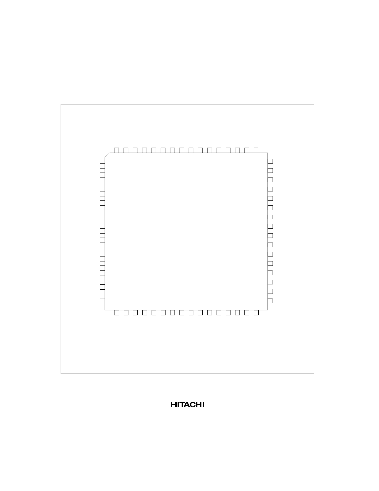
1.3 Pin Arrangement and Functions
1.3.1 Pin Arrangement
The H8/3644 Series pin arrangement is shown in figures 1.2 (FP-64A), 1.3 (DP-64S), and 1.4
(TFP-80C).
PB1/AN
PB0/AN
P9
0
AV
TEST
OSC
OSC
/FV
V
RES
PP
P9
P9
P9
P9
IRQ
SS
X
X
SS
/TRGV
3
2
/IRQ
6
P1
56
1
/IRQ
5
P1
55
/PWM
4
P1
54
2
3
4
5
6
7
/AN
/AN
/AN
/AN
/AN
/AN
2
3
4
5
6
PB
PB
PB
PB
PB
64
64
62
61
1
1
2
0
60
7
PB
59
/IRQ
7
AVCCP1
58
57
3
4
5
2
6
1
7
8
1
9
2
10
*
11
12
1
13
2
14
3
15
4
16
0
17
18
19
20
21
22
23
24
25
26
27
1
/TMOW
/SCK
0
0
P1
P3
53
52
28
29
/SI
P3
51
30
1
1
/SO
/TXD
1
2
2
P3
P2
50
49
48
P21/RXD
47
P2
/SCK
0
3
46
P8
7
45
P86/FTID
44
P8
/FTIC
5
43
P8
/FTIB
4
42
P8
/FTIA
3
41
P8
/FTOB
2
40
P8
/FTOA
1
39
P8
/FTCI
0
38
P7
7
37
P76/TMOV
36
P7
/TMCIV
5
35
P7
/TMRIV
4
34
P7
3
33
V
31
32
CC
0
/INT
0
P5
1
/INT
1
P5
P60P61P62P63P64P65P66P6
7
Note: * There is no P90 function in the flash memory version.
Figure 1.2 Pin Arrangement (FP-64A: Top View)
6
2
/INT
2
P5
3
/INT
3
P5
4
/INT
4
P5
/TMIB
6
/ADTRG
5
/INT
6
/INT
5
P5
P5
7
/INT
7
P5
Page 18

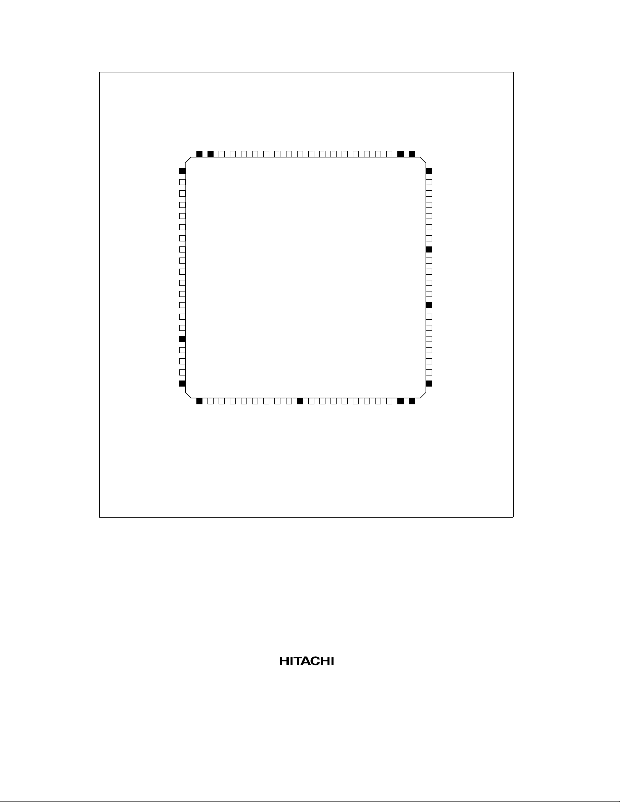
P17/IRQ3/TRGV
AV
CC
PB7/AN
PB6/AN
PB5/AN
PB4/AN
PB3/AN
PB2/AN
PB1/AN
PB0/AN
AV
SS
TEST
X
X
V
SS
OSC
OSC
RES
/FV
P9
0
PP
P9
P9
P9
P9
IRQ
P6
P6
P6
P6
P6
P6
P6
P6
1
2
3
7
4
6
5
5
6
4
7
3
8
2
9
1
10
0
11
12
13
2
14
1
15
16
1
17
2
18
*
19
20
1
21
2
22
3
23
4
24
0
25
0
26
1
27
2
28
3
29
4
30
5
31
6
32
7
64
63
62
61
60
59
58
57
56
55
54
53
52
51
50
49
48
47
46
45
44
43
42
41
40
39
38
37
36
35
34
33
/IRQ
P1
6
2
P15/IRQ
1
P14/PWM
/TMOW
P1
0
/SCK
P3
0
1
P31/SI
1
P32/SO
1
P22/TXD
/RXD
P2
1
/SCK
P2
0
3
P8
7
P86/FTID
/FTIC
P8
5
/FTIB
P8
4
/FTIA
P8
3
/FTOB
P8
2
/FTOA
P8
1
/FTCI
P8
0
P7
7
P76/TMOV
/TMCIV
P7
5
/TMRIV
P7
4
P7
3
V
CC
P57/INT
7
P56/INT6/TMIB
/INT5/ADTRG
P5
5
/INT
P5
4
4
P53/INT
3
P52/INT
2
P51/INT
1
P50/INT
0
Note: * There is no P90 function in the flash memory version.
Figure 1.3 Pin Arrangement (DP-64S: Top View)
7
Page 19
2
/AN
2
NCNCPB
3
/AN
3
PB
4
/AN
4
PB
5
/AN
5
PB
6
/AN
6
PB
7
/AN
7
PB
/TRGV
3
/IRQ
7
AVCCP1
2
/IRQ
6
P1
1
/IRQ
5
P1
/PWM
/TMOW
4
0
P1
P1
1
/SCK
/SI
0
P3
P3
1
1
/SO
/TXD
1
2
2
NC
P2
NC
P3
PB
PB0/AN
P9
0
NC
/AN
1
AV
SS
TEST
X
X
V
SS1
OSC
OSC
V
SS2
RES
/FVPP*
P9
P9
NC
P9
P9
IRQ
NC
80797877767574737271706968676665646362
1
2
1
3
0
4
5
6
2
7
1
8
9
1
10
2
11
12
13
14
1
15
2
16
17
3
18
4
19
0
20
21222324252627282930313233343536373839
0
1
2
3
/INT
2
P5
/INT
3
P5
4
/INT
4
/ADTRG
P5
/INT
5
5
/TMIB
6
/INT
6
P5
0P61P62P63P64P65P66P67
NC
P6
NC
/INT
0
P5
/INT
1
P5
7
/INT
7
P5
NC
61
60
59
58
57
56
55
54
53
52
51
50
49
48
47
46
45
44
43
42
41
40
NC
NC
P2
/RXD
1
P2
/SCK
0
P8
3
7
P86/FTID
P8
/FTIC
5
P8
/FTIB
4
NC
P8
/FTIA
3
P8
/FTOB
2
P8
/FTOA
1
P8
/FTCI
0
NC
P7
7
P76/TMOV
P7
/TMCIV
5
P7
/TMRIV
4
P7
3
V
CC
NC
P5
Note: * There is no P90 function in the flash memory version.
Figure 1.4 Pin Arrangement (TFP-80C: Top View)
8
Page 20

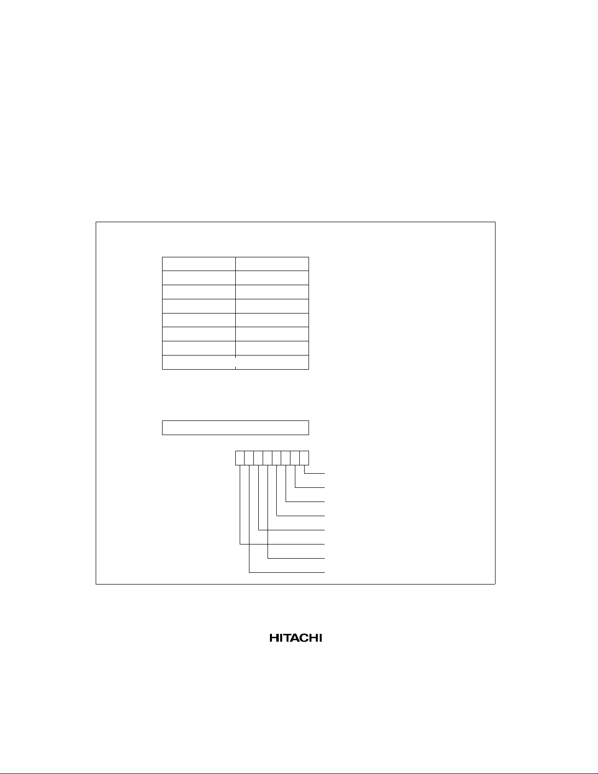
1.3.2 Pin Functions
Table 1.2 outlines the pin functions of the H8/3644 Series.
Table 1.2 Pin Functions
Pin No.
Type Symbol FP-64A DP-64S TFP-80C I/O Name and Functions
Power
source pins
Clock pins OSC
V
CC
V
SS
AV
CC
AV
SS
OSC
33 41 42 Input Power supply: All VCC pins
should be connected to the user
system V
.
CC
7 15 8, 11 Input Ground: All VSS pins should be
connected to the user system
GND.
58 2 72 Input Analog power supply: This is
the power supply pin for the A/D
converter. When the A/D
converter is not used, connect
this pin to the user system V
3 11 4 Input Analog ground: This is the A/D
converter ground pin. It should be
connected to the user system
GND.
8 16 9 Input System clock: These pins
1
connect to a crystal or ceramic
oscillator, or can be used to input
an external clock.
9 17 10 Output
2
See section 4, Clock Pulse
Generators, for a typical
connection diagram.
.
CC
System
control
X
1
6 14 7 Input Subclock: These pins connect to
a 32.768-kHz crystal oscillator.
X
2
5 13 6 Output
See section 4, Clock Pulse
Generators, for a typical
connection diagram.
RES 10 18 12 Input Reset: When this pin is driven
low, the chip is reset
TEST 4 12 5 Input Test: This is a test pin, not for
use in application systems. It
should be connected to V
.
SS
9
Page 21

Table 1.2 Pin Functions (cont)
Pin No.
Type Symbol FP-64A DP-64S TFP-80C I/O Name and Functions
Interrupt
pins
IRQ
IRQ
IRQ
IRQ
INT
INT
16
0
55
1
56
2
57
3
to
7
0
32 to 25 40 to 33 38 to 31 Input INT interrupt request 0 to 7:
24
63
64
1
19
69
70
71
Timer pins TMOW 53 61 67 Output Clock output: This is an output
TMIB 31 39 37 Input Timer B1 event counter input:
TMOV 37 45 46 Output Timer V output: This is an output
TMCIV 36 44 45 Input Timer V event input: This is an
TMRIV 35 43 44 Input Timer V counter reset: This is a
TRGV 57 1 71 Input Timer V counter trigger input:
FTCI 39 47 49 Input Timer X clock input: This is an
FTOA 40 48 50 Output Timer X output compare A
FTOB 41 49 51 Output Timer X output compare B
Input IRQ interrupt request 0 to 3:
These are input pins for edgesensitive external interrupts, with
a selection of rising or falling
edge
These are input pins for edgesensitive external interrupts, with
a selection of rising or falling
edge
pin for waveforms generated by
the timer A output circuit
This is an event input pin for input
to the timer B1 counter
pin for waveforms generated by
the timer V output compare
function
event input pin for input to the
timer V counter
counter reset input pin for timer V
This is a trigger input pin for the
timer V counter and realtime
output port
external clock input pin for input
to the timer X counter
output: This is an output pin for
timer X output compare A
output: This is an output pin for
timer X output compare B
10
Page 22

Table 1.2 Pin Functions (cont)
Pin No.
Type Symbol FP-64A DP-64S TFP-80C I/O Name and Functions
Timer pins FTIA 42 50 52 Input Timer X input capture A input:
This is an input pin for timer X
input capture A
FTIB 43 51 54 Input Timer X input capture B input:
This is an input pin for timer X
input capture B
FTIC 44 52 55 Input Timer X input capture C input:
This is an input pin for timer X
input capture C
FTID 45 53 56 Input Timer X input capture D input:
This is an input pin for timer X
input capture D
14-bit
PWM pin
I/O ports PB7 to
PWM 54 62 68 Output 14-bit PWM output: This is an
output pin for waveforms
generated by the 14-bit PWM
PB
0
P17 to
P1
,
4
P1
0
59 to 64,
1 to 2
57 to 53 1,
3 to 10 73 to 78
2, 3
71 to 67 I/O Port 1: This is a 5-bit I/O port.
64 to 61
Input Port B: This is an 8-bit input port
Input or output can be designated
for each bit by means of port
control register 1 (PCR1)
P22 to
P2
0
49 to 47 57 to 55 63, 5958I/O Port 2: This is a 3-bit I/O port.
Input or output can be designated
for each bit by means of port
control register 2 (PCR2)
P32 to
P3
0
50 to 52 58 to 60 64 to 66 I/O Port 3: This is a 3-bit I/O port.
Input or output can be designated
for each bit by means of port
control register 3 (PCR3)
P57 to
P5
0
32 to 25 40 to 33 38 to 31 I/O Port 5: This is an 8-bit I/O port.
Input or output can be designated
for each bit by means of port
control register 5 (PCR5)
P67 to
P6
0
24 to 17 32 to 25 29 to 22 I/O Port 6: This is an 8-bit I/O port.
Input or output can be designated
for each bit by means of port
control register 6 (PCR6)
11
Page 23

Table 1.2 Pin Functions (cont)
Pin No.
Type Symbol FP-64A DP-64S TFP-80C I/O Name and Functions
I/O ports P77 to
P7
3
P87 to
P8
0
P94 to
P9
0
Serial com-
SI
1
munication
interface
(SCI)
SO
1
SCK
RXD 48 56 59 Input SCI3 receive data input:
TXD 49 57 63 Output SCI3 transmit data output:
SCK
A/D
converter
AN7 to
AN
0
ADTRG 30 38 36 Input A/D converter trigger input:
38 to 34 46 to 42 47 to 43 I/O Port 7: This is a 5-bit I/O port.
Input or output can be designated
for each bit by means of port
control register 7 (PCR7)
46 to 39 54 to 47 57 to 54,
52 to 49
I/O Port 8: This is an 8-bit I/O port.
Input or output can be designated
for each bit by means of port
control register 8 (PCR8)
15 to 11 23 to 19 18, 17
15 to 13
I/O Port 9: This is a 5-bit I/O port.
Input or output can be designated
for each bit by means of port
control register 9 (PCR9)
Note: There is no P9
the flash memory version
since P9
FV
pin.
PP
51 59 65 Input SCI1 receive data input:
This is the SCI1 data input pin
50 58 64 Output SCI1 transmit data output:
This is the SCI1 data output pin
52 60 66 I/O SCI1 clock I/O:
1
This is the SCI1 clock I/O pin
This is the SCI3 data input pin
This is the SCI3 data output pin
47 55 58 I/O SCI3 clock I/O:
3
This is the SCI3 clock I/O pin
59 to 64,
1 to 2
3 to 10 73 to 78
2, 3
Input Analog input channels 11 to 0:
These are analog data input
channels to the A/D converter
This is the external trigger input
pin to the A/D converter
is used as the
0
function in
0
12
Page 24

Table 1.2 Pin Functions (cont)
Pin No.
Type Symbol FP-64A DP-64S TFP-80C I/O Name and Functions
Flash
memory
Other NC — — 1, 16,
FV
PP
11 19 13 Input On-board-programmable flash
memory power supply:
Connected to the flash memory
programming power supply
(+12 V). When the flash memory
is not being programmed,
connect to the user system V
In versions other than the on-chip
flash memory version, this pin is
P9
0
— Non-connected pins: These
20, 21,
pins must be left unconnected
30, 39,
40, 41,
48, 53,
60 to 62,
79, 80
.
CC
13
Page 25

Section 2 CPU
2.1 Overview
The H8/300L CPU has sixteen 8-bit general registers, which can also be paired as eight 16-bit
registers. Its concise instruction set is designed for high-speed operation.
2.1.1 Features
Features of the H8/300L CPU are listed below.
• General-register architecture
Sixteen 8-bit general registers, also usable as eight 16-bit general registers
• Instruction set with 55 basic instructions, including:
Multiply and divide instructions
Powerful bit-manipulation instructions
• Eight addressing modes
Register direct
Register indirect
Register indirect with displacement
Register indirect with post-increment or pre-decrement
Absolute address
Immediate
Program-counter relative
Memory indirect
• 64-kbyte address space
• High-speed operation
All frequently used instructions are executed in two to four states
High-speed arithmetic and logic operations
8- or 16-bit register-register add or subtract: 0.4 µs (operating at ø = 5 MHz)
0.25 µs (operating at ø = 8 MHz)*
8 × 8-bit multiply: 2.8 µs (operating at ø = 5 MHz)
1.75 µs (operating at ø = 8 MHz)*
16 ÷ 8-bit divide: 2.8 µs (operating at ø = 5 MHz)
1.75 µs (operating at ø = 8 MHz)*
Note: * F-ZTAT version only.
• Low-power operation modes
SLEEP instruction for transfer to low-power operation
Note: * These values are at ø = 5 MHz.
15
Page 26
2.1.2 Address Space
The H8/300L CPU supports an address space of up to 64 kbytes for storing program code and
data.
See 2.8, Memory Map, for details of the memory map.
2.1.3 Register Configuration
Figure 2.1 shows the register structure of the H8/300L CPU. There are two groups of registers: the
general registers and control registers.
General registers (Rn)
7070
R0H
R1H
R2H
R3H
R4H
R5H
R6H
R7H
(SP)
R0L
R1L
R2L
R3L
R4L
R5L
R6L
R7L
SP: Stack pointer
16
Control registers (CR)
15 0
PC
75321064
CCR I U H U N Z V C
Figure 2.1 CPU Registers
PC: Program counter
CCR: Condition code register
Carry flag
Overflow flag
Zero flag
Negative flag
Half-carry flag
Interrupt mask bit
User bit
User bit
Page 27

2.2 Register Descriptions
2.2.1 General Registers
All the general registers can be used as both data registers and address registers.
When used as data registers, they can be accessed as 16-bit registers (R0 to R7), or the high bytes
(R0H to R7H) and low bytes (R0L to R7L) can be accessed separately as 8-bit registers.
When used as address registers, the general registers are accessed as 16-bit registers (R0 to R7).
R7 also functions as the stack pointer (SP), used implicitly by hardware in exception processing
and subroutine calls. When it functions as the stack pointer, as indicated in figure 2.2, SP (R7)
points to the top of the stack.
Lower address side [H'0000]
Unused area
SP (R7)
Stack area
Upper address side [H'FFFF]
Figure 2.2 Stack Pointer
2.2.2 Control Registers
The CPU control registers include a 16-bit program counter (PC) and an 8-bit condition code
register (CCR).
Program Counter (PC): This 16-bit register indicates the address of the next instruction the CPU
will execute. All instructions are fetched 16 bits (1 word) at a time, so the least significant bit of
the PC is ignored (always regarded as 0).
17
Page 28

Condition Code Register (CCR): This 8-bit register contains internal status information,
including the interrupt mask bit (I) and half-carry (H), negative (N), zero (Z), overflow (V), and
carry (C) flags. These bits can be read and written by software (using the LDC, STC, ANDC,
ORC, and XORC instructions). The N, Z, V, and C flags are used as branching conditions for
conditional branching (Bcc) instructions.
Bit 7—Interrupt Mask Bit (I): When this bit is set to 1, interrupts are masked. This bit is set to 1
automatically at the start of exception handling. The interrupt mask bit may be read and written by
software. For further details, see section 3.3, Interrupts.
Bit 6—User Bit (U): Can be used freely by the user.
Bit 5—Half-Carry Flag (H): When the ADD.B, ADDX.B, SUB.B, SUBX.B, CMP.B, or NEG.B
instruction is executed, this flag is set to 1 if there is a carry or borrow at bit 3, and is cleared to 0
otherwise.
The H flag is used implicitly by the DAA and DAS instructions.
When the ADD.W, SUB.W, or CMP.W instruction is executed, the H flag is set to 1 if there is a
carry or borrow at bit 11, and is cleared to 0 otherwise.
Bit 4—User Bit (U): Can be used freely by the user.
Bit 3—Negative Flag (N): Indicates the most significant bit (sign bit) of the result of an
instruction.
Bit 2—Zero Flag (Z): Set to 1 to indicate a zero result, and cleared to 0 to indicate a non-zero
result.
Bit 1—Overflow Flag (V): Set to 1 when an arithmetic overflow occurs, and cleared to 0 at other
times.
Bit 0—Carry Flag (C): Set to 1 when a carry occurs, and cleared to 0 otherwise. Used by:
• Add instructions, to indicate a carry
• Subtract instructions, to indicate a borrow
• Shift/rotate carry
The carry flag is also used as a bit accumulator by bit manipulation instructions.
Some instructions leave some or all of the flag bits unchanged.
Refer to the H8/300L Series Programming Manual for the action of each instruction on the flag
bits.
18
Page 29

2.2.3 Initial Register Values
In reset exception handling, the program counter (PC) is initialized by a vector address (H'0000)
load, and the I bit in the CCR is set to 1. The other CCR bits and the general registers are not
initialized. In particular, the stack pointer (R7) is not initialized. The stack pointer should be
initialized by software, by the first instruction executed after a reset.
2.3 Data Formats
The H8/300L CPU can process 1-bit data, 4-bit (BCD) data, 8-bit (byte) data, and 16-bit (word)
data.
The H8/300L CPU can process 1-bit, 4-bit BCD, 8-bit (byte), and 16-bit (word) data. 1-bit data is
handled by bit manipulation instructions, and is accessed by being specified as bit n (n = 0, 1, 2, ...
7) in the operand data (byte).
Byte data is handled by all arithmetic and logic instructions except ADDS and SUBS. Word data
is handled by the MOV.W, ADD.W, SUB.W, CMP.W, ADDS, SUBS, MULXU ( b bits × 8 bits),
and DIVXU (16 bits ÷ 8 bits) instructions.
With the DAA and DAS decimal adjustment instructions, byte data is handled as two 4-bit BCD
data units.
19
Page 30

2.3.1 Data Formats in General Registers
Data of all the sizes above can be stored in general registers as shown in figure 2.3.
Data Type Register No. Data Format
70
1-bit data RnH
1-bit data RnL
Byte data RnH
Byte data RnL
Word data Rn
76543210 don’t care
70
76543210don’t care
70
MSB LSB
70
don’t care
15 0
MSB LSB
MSB LSB
don’t care
4-bit BCD data RnH
4-bit BCD data RnL
Legend:
Upper byte of general register
RnH:
Lower byte of general register
RnL:
Most significant bit
MSB:
Least significant bit
LSB:
20
7034
Upper digit Lower digit
70
don’t care
Upper digit Lower digit
Figure 2.3 General Register Data Formats
don’t care
34
Page 31

2.3.2 Memory Data Formats
Figure 2.4 indicates the data formats in memory. For access by the H8/300L CPU, word data
stored in memory must always begin at an even address. When word data beginning at an odd
address is accessed, the least significant bit is regarded as 0, and the word data beginning at the
preceding address is accessed. The same applies to instruction codes.
1-bit data
Byte data
Word data
Byte data (CCR) on stack
Word data on stack
CCR: Condition code register
Note: Ignored on return*
AddressData Type
Address n
Address n
Even address
Odd address
Even address
Odd address
Even address
Odd address
Data Format
70
76543210
MSB LSB
MSB
MSB LSBCCR
MSB LSB
MSB
Upper 8 bits
Lower 8 bits
*
CCR
LSB
LSB
Figure 2.4 Memory Data Formats
When the stack is accessed using R7 as an address register, word access should always be
performed. The CCR is stored as word data with the same value in the upper 8 bits and the lower 8
bits. On return, the lower 8 bits are ignored.
21
Page 32

2.4 Addressing Modes
2.4.1 Addressing Modes
The H8/300L CPU supports the eight addressing modes listed in table 2.1. Each instruction uses a
subset of these addressing modes.
Table 2.1 Addressing Modes
No. Address Modes Symbol
1 Register direct Rn
2 Register indirect @Rn
3 Register indirect with displacement @(d:16, Rn)
4 Register indirect with post-increment
Register indirect with pre-decrement
5 Absolute address @aa:8 or @aa:16
6 Immediate #xx:8 or #xx:16
7 Program-counter relative @(d:8, PC)
8 Memory indirect @@aa:8
1. Register Direct—Rn: The register field of the instruction specifies an 8- or 16-bit general
register containing the operand.
@Rn+
@–Rn
Only the MOV.W, ADD.W, SUB.W, CMP.W, ADDS, SUBS, MULXU (8 bits × 8 bits), and
DIVXU (16 bits ÷ 8 bits) instructions have 16-bit operands.
2. Register Indirect—@Rn: The register field of the instruction specifies a 16-bit general
register containing the address of the operand in memory.
3. Register Indirect with Displacement—@(d:16, Rn): The instruction has a second word
(bytes 3 and 4) containing a displacement which is added to the contents of the specified
general register to obtain the operand address in memory.
This mode is used only in MOV instructions. For the MOV.W instruction, the resulting address
must be even.
22
Page 33

4. Register Indirect with Post-Increment or Pre-Decrement—@Rn+ or @–Rn:
• Register indirect with post-increment—@Rn+
The @Rn+ mode is used with MOV instructions that load registers from memory.
The register field of the instruction specifies a 16-bit general register containing the address
of the operand. After the operand is accessed, the register is incremented by 1 for MOV.B
or 2 for MOV.W, and the result of the addition is stored in the register. For MOV.W, the
original contents of the 16-bit general register must be even.
• Register indirect with pre-decrement—@–Rn
The @–Rn mode is used with MOV instructions that store register contents to memory.
The register field of the instruction specifies a 16-bit general register which is decremented
by 1 or 2 to obtain the address of the operand in memory. The register retains the
decremented value. The size of the decrement is 1 for MOV.B or 2 for MOV.W. For
MOV.W, the original contents of the register must be even.
5. Absolute Address—@aa:8 or @aa:16: The instruction specifies the absolute address of the
operand in memory.
The absolute address may be 8 bits long (@aa:8) or 16 bits long (@aa:16). The MOV.B and bit
manipulation instructions can use 8-bit absolute addresses. The MOV.B, MOV.W, JMP, and
JSR instructions can use 16-bit absolute addresses.
For an 8-bit absolute address, the upper 8 bits are assumed to be 1 (H'FF). The address range is
H'FF00 to H'FFFF (65280 to 65535).
6. Immediate—#xx:8 or #xx:16: The second byte (#xx:8) or the third and fourth bytes (#xx:16)
of the instruction code are used directly as the operand. Only MOV.W instructions can be used
with #xx:16.
The ADDS and SUBS instructions implicitly contain the value 1 or 2 as immediate data. Some
bit manipulation instructions contain 3-bit immediate data in the second or fourth byte of the
instruction, specifying a bit number.
7. Program-Counter Relative—@(d:8, PC): This mode is used in the Bcc and BSR
instructions. An 8-bit displacement in byte 2 of the instruction code is sign-extended to 16 bits
and added to the program counter contents to generate a branch destination address, and the PC
contents to be added are the start address of the next instruction, so that the possible branching
range is –126 to +128 bytes (–63 to +64 words) from the branch instruction. The displacement
should be an even number.
23
Page 34

8. Memory Indirect—@@aa:8: This mode can be used by the JMP and JSR instructions. The
second byte of the instruction code specifies an 8-bit absolute address. This specifies an
operand in memory, and a branch is performed with the contents of this operand as the branch
address.
The upper 8 bits of the absolute address are assumed to be 0 (H'00), so the address range is
from H'0000 to H'00FF (0 to 255). Note that with the H8/300L Series, the lower end of the
address area is also used as a vector area. See 3.3, Interrupts, for details on the vector area.
If an odd address is specified as a branch destination or as the operand address of a MOV.W
instruction, the least significant bit is regarded as 0, causing word access to be performed at the
address preceding the specified address. See 2.3.2, Memory Data Formats, for further information.
2.4.2 Effective Address Calculation
Table 2.2 shows how effective addresses are calculated in each of the addressing modes.
Arithmetic and logic instructions use register direct addressing (1). The ADD.B, ADDX, SUBX,
CMP.B, AND, OR, and XOR instructions can also use immediate addressing (6).
Data transfer instructions can use all addressing modes except program-counter relative (7) and
memory indirect (8).
Bit manipulation instructions use register direct (1), register indirect (2), or 8-bit absolute
addressing (5) to specify a byte operand, and 3-bit immediate addressing (6) to specify a bit
position in that byte. The BSET, BCLR, BNOT, and BTST instructions can also use register direct
addressing (1) to specify the bit position.
24
Page 35

Table 2.2 Effective Address Calculation
Addressing Mode and
No.
Instruction Format
1
Register indirect, Rn
op rm rn
2
Register indirect, @Rn
op rm
3
Register indirect with
displacement, @(d:16, Rn)
op rm
4
Register indirect with
post-increment, @Rn+
op rm
Register indirect with
pre-decrement, @–Rn
op rm
87 34015
disp
Effective Address
Calculation Method Effective Address (EA)
30rn30
rm
Operand is contents of
registers indicated by rm/rn
015
Contents (16 bits) of
register indicated by rm
76 34015
015
Contents (16 bits) of
register indicated by rm
76 34015
015
015
disp
015
Contents (16 bits) of
register indicated by rm
76 34015
015
1 or 2
015
Contents (16 bits) of
register indicated by rm
76 34015
015
Incremented or
decremented by 1 if
operand is byte size,
1 or 2
and by 2 if word size
25
Page 36

Table 2.2 Effective Address Calculation (cont)
Addressing Mode and
No.
Instruction Format
5
Absolute address
@aa:8
op
@aa:16
6
Immediate
#xx:8
op
#xx:16
87 015
op
abs
87 015
op
IMM
abs
IMM
Effective Address
Calculation Method Effective Address (EA)
87 015
H'FF
015
015
Operand is 1- or 2-byte
immediate data
015
7
26
Program-counter relative
@(d:8, PC)
7015
8
op disp
PC contents
Sign
extension
015
015
disp
Page 37

Table 2.2 Effective Address Calculation (cont)
Addressing Mode and
No.
Instruction Format
8
Memory indirect, @@aa:8
87 015
op
Legend:
rm, rn: Register field
op: Operation field
disp: Displacement
IMM: Immediate data
abs: Absolute address
abs
Effective Address
Calculation Method Effective Address (EA)
87 015
H'00
abs
Memory contents
(16 bits)
015
27
Page 38

2.5 Instruction Set
The H8/300L Series can use a total of 55 instructions, which are grouped by function in table 2.3.
Table 2.3 Instruction Set
Function Instructions Number
Data transfer MOV, PUSH*
1
Arithmetic operations ADD, SUB, ADDX, SUBX, INC, DEC, ADDS,
SUBS, DAA, DAS, MULXU, DIVXU, CMP, NEG
Logic operations AND, OR, XOR, NOT 4
Shift SHAL, SHAR, SHLL, SHLR, ROTL, ROTR,
ROTXL, ROTXR
Bit manipulation BSET, BCLR, BNOT, BTST, BAND, BIAND, BOR,
BIOR, BXOR, BIXOR, BLD, BILD, BST, BIST
Branch Bcc*2, JMP, BSR, JSR, RTS 5
System control RTE, SLEEP, LDC, STC, ANDC, ORC, XORC, NOP 8
Block data transfer EEPMOV 1
Notes: 1. PUSH Rn is equivalent to MOV.W Rn, @–SP.
POP Rn is equivalent to MOV.W @SP+, Rn.
2. Bcc is a conditional branch instruction. The same applies to machine language.
, POP*
1
1
14
8
14
Total: 55
Tables 2.4 to 2.11 show the function of each instruction. The notation used is defined next.
28
Page 39

Notation
Rd General register (destination)
Rs General register (source)
Rn General register
(EAd), <Ead> Destination operand
(EAs), <Eas> Source operand
CCR Condition code register
N N (negative) flag of CCR
Z Z (zero) flag of CCR
V V (overflow) flag of CCR
C C (carry) flag of CCR
PC Program counter
SP Stack pointer
#IMM Immediate data
disp Displacement
+ Addition
– Subtraction
× Multiplication
÷ Division
∧ AND logical
∨ OR logical
⊕ Exclusive OR logical
→ Move
~ Logical negation (logical complement)
:3 3-bit length
:8 8-bit length
:16 16-bit length
( ), < > Contents of operand indicated by effective address
29
Page 40

2.5.1 Data Transfer Instructions
Table 2.4 describes the data transfer instructions. Figure 2.5 shows their object code formats.
Table 2.4 Data Transfer Instructions
Instruction Size* Function
MOV B/W (EAs) → Rd, Rs → (EAd)
Moves data between two general registers or between a general
register and memory, or moves immediate data to a general register.
The Rn, @Rn, @(d:16, Rn), @aa:16, #xx:16, @–Rn, and @Rn+
addressing modes are available for word data. The @aa:8 addressing
mode is available for byte data only.
The @–R7 and @R7+ modes require a word-size specification.
POP W
PUSH W
Notes: * Size: Operand size
B: Byte
W: Word
@SP+ → Rn
Pops a general register from the stack. Equivalent to MOV.W @SP+,
Rn.
Rn → @–SP
Pushes general register onto the stack. Equivalent to MOV.W Rn,
@–SP.
Certain precautions are required in data access. See 2.9.1, Notes on Data Access, for details.
30
Page 41

15 087
op rm rn
15 087
op rm rn
15 087
op rm rn
disp
MOV
Rm→Rn
@Rm←→Rn
@(d:16, Rm)←→Rn
15 087
op rm rn
15 087
op rn abs
15 087
op rn
abs
15 087
op rn IMM
15 087
op rn
IMM
15 087
op rn
Legend:
op:
rm, rn:
disp:
abs:
IMM:
Operation field
Register field
Displacement
Absolute address
Immediate data
111
@Rm+→Rn, or
Rn →@–Rm
@aa:8←→Rn
@aa:16←→Rn
#xx:8→Rn
#xx:16→Rn
PUSH, POP
@SP+ Rn, or
→
Rn @–SP
→
Figure 2.5 Data Transfer Instruction Codes
31
Page 42

2.5.2 Arithmetic Operations
Table 2.5 describes the arithmetic instructions.
Table 2.5 Arithmetic Instructions
Instruction Size* Function
ADD
SUB
ADDX
SUBX
INC
DEC
ADDS
SUBS
DAA
DAS
MULXU B
DIVXU B
CMP B/W
B/W Rd ± Rs → Rd, Rd + #IMM → Rd
Performs addition or subtraction on data in two general registers, or
addition on immediate data and data in a general register. Immediate
data cannot be subtracted from data in a general register. Word data
can be added or subtracted only when both words are in general
registers.
B Rd ± Rs ± C → Rd, Rd ± #IMM ± C → Rd
Performs addition or subtraction with carry on data in two general
registers, or addition or subtraction with carry on immediate data and
data in a general register.
B
W
B
Rd ± 1 → Rd
Increments or decrements a general register
Rd ± 1 → Rd, Rd ± 2 → Rd
Adds or subtracts 1 or 2 to or from a general register
Rd decimal adjust → Rd
Decimal-adjusts (adjusts to packed BCD) an addition or subtraction
result in a general register by referring to the CCR
Rd × Rs → Rd
Performs 8-bit × 8-bit unsigned multiplication on data in two general
registers, providing a 16-bit result
Rd ÷ Rs → Rd
Performs 16-bit ÷ 8-bit unsigned division on data in two general
registers, providing an 8-bit quotient and 8-bit remainder
Rd – Rs, Rd – #IMM
Compares data in a general register with data in another general
register or with immediate data, and indicates the result in the CCR.
Word data can be compared only between two general registers.
NEG B
Notes: * Size: Operand size
B: Byte
W: Word
32
0 – Rd → Rd
Obtains the two’s complement (arithmetic complement) of data in a
general register
Page 43

2.5.3 Logic Operations
Table 2.6 describes the four instructions that perform logic operations.
Table 2.6 Logic Operation Instructions
Instruction Size* Function
AND B
OR B
XOR B
NOT B
Notes: * Size: Operand size
B: Byte
Rd ∧ Rs → Rd, Rd ∧ #IMM → Rd
Performs a logical AND operation on a general register and another
general register or immediate data
Rd ∨ Rs → Rd, Rd ∨ #IMM → Rd
Performs a logical OR operation on a general register and another
general register or immediate data
Rd ⊕ Rs → Rd, Rd ⊕ #IMM → Rd
Performs a logical exclusive OR operation on a general register and
another general register or immediate data
~ Rd → Rd
Obtains the one’s complement (logical complement) of general
register contents
2.5.4 Shift Operations
Table 2.7 describes the eight shift instructions.
Table 2.7 Shift Instructions
Instruction Size* Function
SHAL
SHAR
SHLL
SHLR
ROTL
ROTR
ROTXL
ROTXR
Notes: * Size: Operand size
B: Byte
B Rd shift → Rd
Performs an arithmetic shift operation on general register contents
B Rd shift → Rd
Performs a logical shift operation on general register contents
B
B
Rd rotate → Rd
Rotates general register contents
Rd rotate → Rd
Rotates general register contents through the C (carry) bit
33
Page 44

Figure 2.6 shows the instruction code format of arithmetic, logic, and shift instructions.
15 087
op rm rn
15 087
op rn
15 087
op rn
15 087
op
15 087
rn IMM
op rn
15 087
op
15 087
rn IMM
op
Legend:
op:
rm, rn:
IMM:
Operation field
Register field
Immediate data
rm
rm
rn
ADD, SUB, CMP,
ADDX, SUBX (Rm)
ADDS, SUBS, INC, DEC,
DAA, DAS, NEG, NOT
MULXU, DIVXU
ADD, ADDX, SUBX,
CMP (#XX:8)
AND, OR, XOR (Rm)
AND, OR, XOR (#xx:8)
SHAL, SHAR, SHLL, SHLR,
ROTL, ROTR, ROTXL, ROTXR
34
Figure 2.6 Arithmetic, Logic, and Shift Instruction Codes
Page 45

2.5.5 Bit Manipulations
Table 2.8 describes the bit-manipulation instructions. Figure 2.7 shows their object code formats.
Table 2.8 Bit-Manipulation Instructions
Instruction Size* Function
BSET B 1 → (<bit-No.> of <EAd>)
Sets a specified bit in a general register or memory to 1. The bit
number is specified by 3-bit immediate data or the lower three bits of
a general register.
BCLR B 0 → (<bit-No.> of <EAd>)
Clears a specified bit in a general register or memory to 0. The bit
number is specified by 3-bit immediate data or the lower three bits of
a general register.
BNOT B
~ (<bit-No.> of <EAd>) → (<bit-No.> of <EAd>)
Inverts a specified bit in a general register or memory. The bit number
is specified by 3-bit immediate data or the lower three bits of a
general register.
BTST B
BAND B
BIAND B
BOR B
BIOR B C ∨ [~ (<bit-No.> of <EAd>)] → C
Notes: * Size: Operand size
B: Byte
~ (<bit-No.> of <EAd>) → Z
Tests a specified bit in a general register or memory and sets or
clears the Z flag accordingly. The bit number is specified by 3-bit
immediate data or the lower three bits of a general register.
C ∧ (<bit-No.> of <EAd>) → C
ANDs the C flag with a specified bit in a general register or memory,
and stores the result in the C flag.
C ∧ [~ (<bit-No.> of <EAd>)] → C
ANDs the C flag with the inverse of a specified bit in a general
register or memory, and stores the result in the C flag.
The bit number is specified by 3-bit immediate data.
C ∨ (<bit-No.> of <EAd>) → C
ORs the C flag with a specified bit in a general register or memory,
and stores the result in the C flag.
ORs the C flag with the inverse of a specified bit in a general register
or memory, and stores the result in the C flag.
The bit number is specified by 3-bit immediate data.
35
Page 46

Table 2.8 Bit-Manipulation Instructions (cont)
Instruction Size* Function
BXOR B
BIXOR B
BLD B
BILD B
C ⊕ (<bit-No.> of <EAd>) → C
XORs the C flag with a specified bit in a general register or memory,
and stores the result in the C flag.
C ⊕ [~(<bit-No.> of <EAd>)] → C
XORs the C flag with the inverse of a specified bit in a general
register or memory, and stores the result in the C flag.
The bit number is specified by 3-bit immediate data.
(<bit-No.> of <EAd>) → C
Copies a specified bit in a general register or memory to the C flag.
~ (<bit-No.> of <EAd>) → C
Copies the inverse of a specified bit in a general register or memory
to the C flag.
The bit number is specified by 3-bit immediate data.
BST B
BIST B
Notes: * Size: Operand size
B: Byte
C → (<bit-No.> of <EAd>)
Copies the C flag to a specified bit in a general register or memory.
~ C → (<bit-No.> of <EAd>)
Copies the inverse of the C flag to a specified bit in a general register
or memory.
The bit number is specified by 3-bit immediate data.
Certain precautions are required in bit manipulation. See 2.9.2, Notes on Bit Manipulation, for
details.
36
Page 47

15 087
op IMM rn
BSET, BCLR, BNOT, BTST
Operand:
Bit No.:
register direct (Rn)
immediate (#xx:3)
15 087
op rn
15 087
op 0
op
15 087
op 0
15 087
op
op
15 087
op
15 087
op IMM rn
rm
rn
rn
abs
abs
Operand:
Bit No.:
Operand:
0000000IMM
Bit No.:
Operand:
0000000rmop
Bit No.:
Operand:
0000IMM
Bit No.:
Operand:
0000rmop
Bit No.:
register direct (Rn)
register direct (Rm)
register indirect (@Rn)
immediate (#xx:3)
register indirect (@Rn)
register direct (Rm)
absolute (@aa:8)
immediate (#xx:3)
absolute (@aa:8)
register direct (Rm)
BAND, BOR, BXOR, BLD, BST
Operand:
Bit No.:
register direct (Rn)
immediate (#xx:3)
15 087
op 0
15 087
op
Legend:
op:
rm, rn:
abs:
IMM:
Operation field
Register field
Absolute address
Immediate data
Figure 2.7 Bit Manipulation Instruction Codes
rn
0000000IMMop
abs
0000IMMop
Operand:
Bit No.:
Operand:
Bit No.:
register indirect (@Rn)
immediate (#xx:3)
absolute (@aa:8)
immediate (#xx:3)
37
Page 48

15 087
op IMM rn
15 087
op 0
15 087
op
Legend:
op:
Operation field
rm, rn:
Register field
abs:
Absolute address
IMM:
Immediate data
Figure 2.7 Bit Manipulation Instruction Codes (cont)
BIAND, BIOR, BIXOR, BILD, BIST
Operand:
Bit No.:
rn
0000000IMMop
abs
0000IMMop
Operand:
Bit No.:
Operand:
Bit No.:
register direct (Rn)
immediate (#xx:3)
register indirect (@Rn)
immediate (#xx:3)
absolute (@aa:8)
immediate (#xx:3)
38
Page 49

2.5.6 Branching Instructions
Table 2.9 describes the branching instructions. Figure 2.8 shows their object code formats.
Table 2.9 Branching Instructions
Instruction Size* Function
Bcc — Branches to the designated address if condition cc is true. The
branching conditions are given below.
Mnemonic Description Condition
BRA (BT) Always (true) Always
BRN (BF) Never (false) Never
BHI High C ∨ Z = 0
BLS Low or same C ∨ Z = 1
BCC (BHS) Carry clear (high or same) C = 0
BCS (BLO) Carry set (low) C = 1
BNE Not equal Z = 0
BEQ Equal Z = 1
BVC Overflow clear V = 0
BVS Overflow set V = 1
BPL Plus N = 0
BMI Minus N = 1
BGE Greater or equal N ⊕ V = 0
BLT Less than N ⊕ V = 1
BGT Greater than Z ∨ (N ⊕ V) = 0
BLE Less or equal Z ∨ (N ⊕ V) = 1
JMP —
BSR —
JSR —
RTS —
Branches unconditionally to a specified address
Branches to a subroutine at a specified address
Branches to a subroutine at a specified address
Returns from a subroutine
39
Page 50

15 087
op cc disp
15 087
op rm 0
15 087
op
abs
15 087
op abs
15 087
op disp
15 087
op rm 0
15 087
op
abs
000
000
Bcc
JMP (@Rm)
JMP (@aa:16)
JMP (@@aa:8)
BSR
JSR (@Rm)
JSR (@aa:16)
40
15 087
op abs
15 087
op
Legend:
op:
Operation field
cc:
Condition field
rm:
Register field
disp:
Displacement
abs:
Absolute address
Figure 2.8 Branching Instruction Codes
JSR (@@aa:8)
RTS
Page 51

2.5.7 System Control Instructions
Table 2.10 describes the system control instructions. Figure 2.9 shows their object code formats.
Table 2.10 System Control Instructions
Instruction Size* Function
RTE — Returns from an exception-handling routine
SLEEP — Causes a transition from active mode to a power-down mode. See
section 5, Power-Down Modes, for details.
LDC B Rs → CCR, #IMM → CCR
Moves immediate data or general register contents to the condition
code register
STC B CCR → Rd
Copies the condition code register to a specified general register
ANDC B CCR ∧ #IMM → CCR
Logically ANDs the condition code register with immediate data
ORC B CCR ∨ #IMM → CCR
Logically ORs the condition code register with immediate data
XORC B CCR ⊕ #IMM → CCR
Logically exclusive-ORs the condition code register with immediate
data
NOP — PC + 2 → PC
Only increments the program counter
Notes: * Size: Operand size
B: Byte
41
Page 52

15 087
op
15 087
op rn
RTE, SLEEP, NOP
LDC, STC (Rn)
15 087
op IMM
Legend:
op:
Operation field
rn:
Register field
IMM:
Immediate data
ANDC, ORC,
XORC, LDC (#xx:8)
Figure 2.9 System Control Instruction Codes
2.5.8 Block Data Transfer Instruction
Table 2.11 describes the block data transfer instruction. Figure 2.10 shows its object code format.
Table 2.11 Block Data Transfer Instruction
Instruction Size Function
EEPMOV — If R4L ≠ 0 then
repeat @R5+ → @R6+
R4L – 1 → R4L
until R4L = 0
else next;
Block transfer instruction. Transfers the number of data bytes
specified by R4L from locations starting at the address indicated by
R5 to locations starting at the address indicated by R6. After the
transfer, the next instruction is executed.
Certain precautions are required in using the EEPMOV instruction. See 2.9.3, Notes on Use of the
EEPMOV Instruction, for details.
42
Page 53

15 087
op
op
Legend:
op: Operation field
Figure 2.10 Block Data Transfer Instruction Code
43
Page 54

2.6 Basic Operational Timing
CPU operation is synchronized by a system clock (ø) or a subclock (ø
clock signals see section 4, Clock Pulse Generators. The period from a rising edge of ø or ø
). For details on these
SUB
SUB
to
the next rising edge is called one state. A bus cycle consists of two states or three states. The cycle
differs depending on whether access is to on-chip memory or to on-chip peripheral modules.
2.6.1 Access to On-Chip Memory (RAM, ROM)
Access to on-chip memory takes place in two states. The data bus width is 16 bits, allowing access
in byte or word size. Figure 2.11 shows the on-chip memory access cycle.
Bus cycle
ø or ø
SUB
Internal address bus
Internal read signal
Internal data bus
(read access)
T1 state
Address
T2 state
Read data
44
Internal write signal
Internal data bus
(write access)
Figure 2.11 On-Chip Memory Access Cycle
Write data
Page 55

2.6.2 Access to On-Chip Peripheral Modules
On-chip peripheral modules are accessed in two states or three states. The data bus width is 8 bits,
so access is by byte size only. This means that for accessing word data, two instructions must be
used.
Two-State Access to On-Chip Peripheral Modules: Figure 2.12 shows the operation timing in
the case of two-state access to an on-chip peripheral module.
Bus cycle
ø or ø
SUB
Internal address bus
Internal read signal
Internal data bus
(read access)
Internal write signal
Internal data bus
(write access)
T1 state
Address
state
T
2
Read data
Write data
Figure 2.12 On-Chip Peripheral Module Access Cycle (2-State Access)
45
Page 56

Three-State Access to On-Chip Peripheral Modules: Figure 2.13 shows the operation timing in
the case of three-state access to an on-chip peripheral module.
Bus cycle
ø or ø
SUB
Internal
address bus
Internal
read signal
Internal
data bus
(read access)
Internal
write signal
Internal
data bus
(write access)
Figure 2.13 On-Chip Peripheral Module Access Cycle (3-State Access)
2.7 CPU States
T1 state
T2 state T3 state
Address
Read data
Write data
2.7.1 Overview
There are four CPU states: the reset state, program execution state, program halt state, and
exception-handling state. The program execution state includes active (high-speed or mediumspeed) mode and subactive mode. In the program halt state there are a sleep (high-speed or
medium-speed) mode, standby mode, watch mode, and sub-sleep mode. These states are shown in
figure 2.14. Figure 2.15 shows the state transitions.
46
Page 57

CPU state Reset state
The CPU is initialized
Program
execution state
Active
(high speed) mode
The CPU executes successive program
instructions at high speed,
synchronized by the system clock
(medium speed) mode
The CPU executes successive
program instructions at
reduced speed, synchronized
by the system clock
The CPU executes
successive program
instructions at reduced
speed, synchronized
by the subclock
Active
Subactive mode
Low-power
modes
Program halt state
A state in which some
or all of the chip
functions are stopped
to conserve power
Exception-
handling state
A transient state in which the CPU changes
the processing flow due to a reset or an interrupt
Note: See section 5, Power-Down Modes, for details on the modes and their transitions.
Sleep (high-speed)
mode
Sleep (medium-speed)
mode
Standby mode
Watch mode
Subsleep mode
Figure 2.14 CPU Operation States
47
Page 58

Reset state
Reset cleared
Exception-handling state
Reset occurs
Reset
occurs
Program halt state
Reset
occurs
SLEEP instruction executed
Interrupt
source
Exceptionhandling
request
Program execution state
Exceptionhandling
complete
Figure 2.15 State Transitions
2.7.2 Program Execution State
In the program execution state the CPU executes program instructions in sequence.
There are three modes in this state, two active modes (high speed and medium speed) and one
subactive mode. Operation is synchronized with the system clock in active mode (high speed and
medium speed), and with the subclock in subactive mode. See section 5, Power-Down Modes for
details on these modes.
2.7.3 Program Halt State
In the program halt state there are five modes: two sleep modes (high speed and medium speed),
standby mode, watch mode, and subsleep mode. See section 5, Power-Down Modes for details on
these modes.
2.7.4 Exception-Handling State
The exception-handling state is a transient state occurring when exception handling is started by a
reset or interrupt and the CPU changes its normal processing flow. In exception handling caused
by an interrupt, SP (R7) is referenced and the PC and CCR values are saved on the stack.
For details on interrupt handling, see section 3.3, Interrupts.
48
Page 59

2.8 Memory Map
Figure 2.16 shows a memory map of the H8/3644 Series.
H'0000
H'002F
H'0030
H'1FFF
H'2FFF
H'3FFF
H'5FFF
H'7FFF
Interrupt vectors
On-chip ROM
Reserved
H8/3640
8 kbytes
H8/3641
12 kbytes
H8/3642
16 kbytes
H8/3643
24 kbytes
H8/3644
32 kbytes
H'F770
H'F77F
H'FB80
H'FD7F
H'FD80
H'FF7F
H'FF80
H'FF9F
H'FFA0
H'FFFF
Internal I/O registers
(16 bytes)
Reserved
On-chip RAM
Reserved
Internal I/O registers
(128 bytes)
Figure 2.16 H8/3644 Series Memory Map
512 bytes 512 bytes 512 bytes
1 kbyte 1 kbyte
49
Page 60

2.9 Application Notes
2.9.1 Notes on Data Access
1. Access to empty areas
The address space of the H8/300L CPU includes empty areas in addition to the RAM,
registers, and ROM areas available to the user. If these empty areas are mistakenly accessed by
an application program, the following results will occur.
Data transfer from CPU to empty area:
The transferred data will be lost. This action may also cause the CPU to misoperate.
Data transfer from empty area to CPU:
Unpredictable data is transferred.
2. Access to internal I/O registers
Internal data transfer to or from on-chip modules other than the ROM and RAM areas makes
use of an 8-bit data width. If word access is attempted to these areas, the following results will
occur.
Word access from CPU to I/O register area:
Upper byte: Will be written to I/O register.
Lower byte: Transferred data will be lost.
Word access from I/O register to CPU:
Upper byte: Will be written to upper part of CPU register.
Lower byte: Unpredictable data will be written to lower part of CPU register.
Byte size instructions should therefore be used when transferring data to or from I/O registers
other than the on-chip ROM and RAM areas. Figure 2.17 shows the data size and number of states
in which on-chip peripheral modules can be accessed.
50
Page 61

H'0000
H'002F
H'0030
H'7FFF
Interrupt vector area
(48 bytes)
On-chip ROM
Access
Word Byte
States
2
Reserved
H'F770
Internal I/O registers
(16 bytes)
H'F77F
Reserved
H'FB80
On-chip RAM
H'FF7F
H'FF80
H'FF9F
H'FFA0
H'FFFF
Notes: The H8/3644 is shown as an example.
Internal I/O registers in areas assigned to timer X (H'F770 to H'F77F),
*
SCI3 (H'FFA8 to H'FFAD), and timer V (H'FFB8 to H'FFBD) are accessed in three
states.
Reserved
Internal I/O registers
(96 bytes)
1,024 bytes
———
×
———
——
×
×
*
3
2
2 or 3
*
Figure 2.17 Data Size and Number of States for Access to and from
On-Chip Peripheral Modules
51
Page 62

2.9.2 Notes on Bit Manipulation
The BSET, BCLR, BNOT, BST, and BIST instructions read one byte of data, modify the data,
then write the data byte again. Special care is required when using these instructions in cases
where two registers are assigned to the same address, in the case of registers that include writeonly bits, and when the instruction accesses an I/O port.
Order of Operation Operation
1 Read Read byte data at the designated address
2 Modify Modify a designated bit in the read data
3 Write Write the altered byte data to the designated address
Bit Manipulation in Two Registers Assigned to the Same Address
Example 1: timer load register and timer counter
Figure 2.18 shows an example in which two timer registers share the same address. When a bit
manipulation instruction accesses the timer load register and timer counter of a reloadable timer,
since these two registers share the same address, the following operations take place.
Order of Operation Operation
1 Read Timer counter data is read (one byte)
2 Modify The CPU modifies (sets or resets) the bit designated in the instruction
3 Write The altered byte data is written to the timer load register
The timer counter is counting, so the value read is not necessarily the same as the value in the
timer load register. As a result, bits other than the intended bit in the timer load register may be
modified to the timer counter value.
Count clock Timer counter
Reload
Timer load register
R
R:W:Read
Write
W
Internal bus
Figure 2.18 Timer Configuration Example
52
Page 63

Example 2: BSET instruction executed designating port 3
P37 and P36 are designated as input pins, with a low-level signal input at P37 and a high-level
signal at P36. The remaining pins, P35 to P30, are output pins and output low-level signals. In this
example, the BSET instruction is used to change pin P30 to high-level output.
[A: Prior to executing BSET]
P3
7
P3
P3
6
5
P3
4
P3
P3
3
P3
2
P3
1
0
Input/output Input Input Output Output Output Output Output Output
Pin state Low
level
High
level
Low
level
Low
level
Low
level
Low
level
Low
level
Low
level
PCR3 00111111
PDR3 10000000
[B: BSET instruction executed]
BSET #0 , @PDR3
The BSET instruction is executed designating port 3.
[C: After executing BSET]
P3
7
Input/output Input Input Output Output Output Output Output Output
Pin state Low
level
PCR3 00111111
PDR3 0 1000001
P3
High
level
P3
6
5
Low
level
P3
4
Low
level
P3
Low
level
P3
3
Low
level
P3
2
Low
level
P3
1
0
High
level
[D: Explanation of how BSET operates]
When the BSET instruction is executed, first the CPU reads port 3.
Since P37 and P36 are input pins, the CPU reads the pin states (low-level and high-level input).
P35 to P30 are output pins, so the CPU reads the value in PDR3. In this example PDR3 has a value
of H'80, but the value read by the CPU is H'40.
Next, the CPU sets bit 0 of the read data to 1, changing the PDR3 data to H'41. Finally, the CPU
writes this value (H'41) to PDR3, completing execution of BSET.
As a result of this operation, bit 0 in PDR3 becomes 1, and P30 outputs a high-level signal.
However, bits 7 and 6 of PDR3 end up with different values.
53
Page 64

To avoid this problem, store a copy of the PDR3 data in a work area in memory. Perform the bit
manipulation on the data in the work area, then write this data to PDR3.
[A: Prior to executing BSET]
MOV. B #80, R0L
MOV. B R0L, @RAM0
MOV. B R0L, @PDR3
P3
P3
7
6
The PDR3 value (H'80) is written to a work area in
memory (RAM0) as well as to PDR3.
P3
P3
5
4
P3
P3
3
P3
2
1
P3
0
Input/output Input Input Output Output Output Output Output Output
Pin state Low
level
High
level
Low
level
Low
level
Low
level
Low
level
Low
level
Low
level
PCR3 00111111
PDR3 10000000
RAM0 10000000
[B: BSET instruction executed]
BSET #0 , @RAM0
The BSET instruction is executed designating the PDR3
work area (RAM0).
[C: After executing BSET]
MOV. B @RAM0, R0L
The work area (RAM0) value is written to PDR3.
MOV. B R0L, @PDR3
P3
P3
7
6
P3
P3
5
4
P3
P3
3
P3
2
1
P3
0
Input/output Input Input Output Output Output Output Output Output
Pin state Low
level
High
level
Low
level
Low
level
Low
level
Low
level
Low
level
High
level
PCR3 00111111
PDR3 10000001
RAM0 10000001
54
Page 65

Bit Manipulation in a Register Containing a Write-Only Bit
Example 3: BCLR instruction executed designating port 3 control register PCR3
As in the examples above, P37 and P36 are input pins, with a low-level signal input at P37 and a
high-level signal at P36. The remaining pins, P35 to P30, are output pins that output low-level
signals. In this example, the BCLR instruction is used to change pin P30 to an input port. It is
assumed that a high-level signal will be input to this input pin.
[A: Prior to executing BCLR]
P3
7
P3
P3
6
5
P3
4
P3
P3
3
P3
2
P3
1
0
Input/output Input Input Output Output Output Output Output Output
Pin state Low
level
High
level
Low
level
Low
level
Low
level
Low
level
Low
level
Low
level
PCR3 00111111
PDR3 10000000
[B: BCLR instruction executed]
BCLR #0 , @PCR3
The BCLR instruction is executed designating PCR3.
[C: After executing BCLR]
P3
7
Input/output Output Output Output Output Output Output Output Input
Pin state Low
level
PCR3 1 1 111110
PDR3 10000000
P3
High
level
P3
6
5
Low
level
P3
4
Low
level
P3
Low
level
P3
3
Low
level
P3
2
Low
level
P3
1
0
High
level
[D: Explanation of how BCLR operates]
When the BCLR instruction is executed, first the CPU reads PCR3. Since PCR3 is a write-only
register, the CPU reads a value of H'FF, even though the PCR3 value is actually H'3F.
Next, the CPU clears bit 0 in the read data to 0, changing the data to H'FE. Finally, this value
(H'FE) is written to PCR3 and BCLR instruction execution ends.
As a result of this operation, bit 0 in PCR3 becomes 0, making P30 an input port. However, bits 7
and 6 in PCR3 change to 1, so that P37 and P36 change from input pins to output pins.
55
Page 66

To avoid this problem, store a copy of the PCR3 data in a work area in memory. Perform the bit
manipulation on the data in the work area, then write this data to PCR3.
[A: Prior to executing BCLR]
MOV. B #3F, R0L
MOV. B R0L, @RAM0
MOV. B R0L, @PCR3
P3
P3
7
6
The PCR3 value (H'3F) is written to a work area in
memory (RAM0) as well as to PCR3.
P3
P3
5
4
P3
P3
3
P3
2
1
P3
0
Input/output Input Input Output Output Output Output Output Output
Pin state Low
level
High
level
Low
level
Low
level
Low
level
Low
level
Low
level
Low
level
PCR3 00111111
PDR3 10000000
RAM0 00111111
[B: BCLR instruction executed]
BCLR #0 , @RAM0
The BCLR instruction is executed designating the PCR3
work area (RAM0).
[C: After executing BCLR]
MOV. B @RAM0, R0L
The work area (RAM0) value is written to PCR3.
MOV. B R0L, @PCR3
P3
P3
7
6
P3
P3
5
4
P3
P3
3
P3
2
1
P3
0
Input/output Input Input Output Output Output Output Output Output
Pin state Low
level
High
level
Low
level
Low
level
Low
level
Low
level
Low
level
High
level
PCR3 00111110
PDR3 10000000
RAM0 00111110
56
Page 67

Table 2.12 lists the pairs of registers that share identical addresses. Table 2.13 lists the registers
that contain write-only bits.
Table 2.12 Registers with Shared Addresses
Register Name Abbreviation Address
Output compare register AH and output compare register BH (timer X) OCRAH/OCRBH H'F774
Output compare register AL and output compare register BL (timer X) OCRAL/OCRBL H'F775
Timer counter B1 and timer load register B1 (timer B1) TCB1/TLB1 H'FFB3
Port data register 1* PDR1 H'FFD4
Port data register 2* PDR2 H'FFD5
Port data register 3* PDR3 H'FFD6
Port data register 5* PDR5 H'FFD8
Port data register 6* PDR6 H'FFD9
Port data register 7* PDR7 H'FFDA
Port data register 8* PDR8 H'FFDB
Port data register 9* PDR9 H'FFDC
Note: *Port data registers have the same addresses as input pins.
Table 2.13 Registers with Write-Only Bits
Register Name Abbreviation Address
Port control register 1 PCR1 H'FFE4
Port control register 2 PCR2 H'FFE5
Port control register 3 PCR3 H'FFE6
Port control register 5 PCR5 H'FFE8
Port control register 6 PCR6 H'FFE9
Port control register 7 PCR7 H'FFEA
Port control register 8 PCR8 H'FFEB
Port control register 9 PCR9 H'FFEC
PWM control register PWCR H'FFD0
PWM data register U PWDRU H'FFD1
PWM data register L PWDRL H'FFD2
57
Page 68

2.9.3 Notes on Use of the EEPMOV Instruction
• The EEPMOV instruction is a block data transfer instruction. It moves the number of bytes
specified by R4L from the address specified by R5 to the address specified by R6.
→
R5
←
R6
R5 + R4L
→
←
R6 + R4L
• When setting R4L and R6, make sure that the final destination address (R6 + R4L) does not
exceed H'FFFF. The value in R6 must not change from H'FFFF to H'0000 during execution of
the instruction.
→
R5
R5 + R4L
→
H'FFFF
Not allowed
←
R6
←
R6 + R4L
58
Page 69

Section 3 Exception Handling
3.1 Overview
Exception handling is performed in the H8/3644 Series when a reset or interrupt occurs. Table 3.1
shows the priorities of these two types of exception handling.
Table 3.1 Exception Handling Types and Priorities
Priority Exception Source Time of Start of Exception Handling
High Reset Exception handling starts as soon as the reset state is cleared
Interrupt When an interrupt is requested, exception handling starts after
execution of the present instruction or the exception handling
Low
3.2 Reset
3.2.1 Overview
A reset is the highest-priority exception. The internal state of the CPU and the registers of the onchip peripheral modules are initialized.
in progress is completed
3.2.2 Reset Sequence
Reset by RES Pin: As soon as the RES pin goes low, all processing is stopped and the chip enters
the reset state.
To make sure the chip is reset properly, observe the following precautions.
• At power on: Hold the RES pin low until the clock pulse generator output stabilizes.
• Resetting during operation: Hold the RES pin low for at least 10 system clock cycles.
Reset exception handling begins when the RES pin is held low for a given period, then returned to
the high level.
Reset exception handling takes place as follows.
• The CPU internal state and the registers of on-chip peripheral modules are initialized, with the
I bit of the condition code register (CCR) set to 1.
• The PC is loaded from the reset exception handling vector address (H'0000 to H'0001), after
which the program starts executing from the address indicated in PC.
59
Page 70

When system power is turned on or off, the RES pin should be held low.
Figure 3.1 shows the reset sequence starting from RES input.
Reset cleared
Vector fetch
RES
ø
Internal
processing
Program initial
instruction prefetch
Internal
address bus
Internal read
signal
Internal write
signal
Internal data
bus (16-bit)
(1) Reset exception handling vector address (H'0000)
(2) Program start address
(3) First instruction of program
(1)
(2) (3)
(2)
Figure 3.1 Reset Sequence
Reset by Watchdog Timer: The watchdog timer counter (TCW) starts counting up when the
WDON bit is set to 1 in the watchdog timer control/status register (TCSRW). If TCW overflows,
the WRST bit is set to 1 in TCSRW and the chip enters the reset state. While the WRST bit is set
to 1 in TCSRW, when TCW overflows the reset state is cleared and reset exception handling
begins. The same reset exception handling is carried out as for input at the RES pin. For details on
the watchdog timer, see 9.1.1, Watchdog Timer.
60
Page 71

3.2.3 Interrupt Immediately after Reset
After a reset, if an interrupt were to be accepted before the stack pointer (SP: R7) was initialized,
PC and CCR would not be pushed onto the stack correctly, resulting in program runaway. To
prevent this, immediately after reset exception handling all interrupts are masked. For this reason,
the initial program instruction is always executed immediately after a reset. This instruction should
initialize the stack pointer (e.g. MOV.W #xx: 16, SP).
3.3 Interrupts
3.3.1 Overview
The interrupt sources include 12 external interrupts (IRQ3 to IRQ0, INT7 to INT0) and 21 internal
interrupts from on-chip peripheral modules. Table 3.2 shows the interrupt sources, their priorities,
and their vector addresses. When more than one interrupt is requested, the interrupt with the
highest priority is processed.
The interrupts have the following features:
• Internal and external interrupts can be masked by the I bit in CCR. When the I bit is set to 1,
interrupt request flags can be set but the interrupts are not accepted.
• IRQ3 to IRQ0 and INT7 to INT0 can be set independently to either rising edge sensing or falling
edge sensing.
61
Page 72

Table 3.2 Interrupt Sources and Their Priorities
Interrupt Source Interrupt Vector Number Vector Address Priority
RES Reset 0 H'0000 to H'0001 High
IRQ
0
IRQ
1
IRQ
2
IRQ
3
INT
0
INT
1
INT
2
INT
3
INT
4
INT
5
INT
6
INT
7
Timer A Timer A overflow 10 H'0014 to H'0015
Timer B1 Timer B1 overflow 11 H'0016 to H'0017
Timer X Timer X input capture A 16 H'0020 to H'0021
Timer V Timer V compare match A 17 H'0022 to H'0023
SCI1 SCI1 transfer complete 19 H'0026 to H'0027
SCI3 SCI3 transmit end 21 H'002A to H'002B
A/D A/D conversion end 22 H'002C to H'002D
(SLEEP instruction
executed)
Note: Vector addresses H'0002 to H'0007, H'0012 to H'0013, H'0018 to H'001F, H'0024 to
H'0025, H'0028 to H'0029 are reserved and cannot be used.
62
IRQ
IRQ
IRQ
IRQ
INT
INT
INT
INT
INT
INT
INT
INT
0
1
2
3
0
1
2
3
4
5
6
7
4 H'0008 to H'0009
5 H'000A to H'000B
6 H'000C to H'000D
7 H'000E to H'000F
8 H'0010 to H'0011
Timer X input capture B
Timer X input capture C
Timer X input capture D
Timer X compare match A
Timer X compare match B
Timer X overflow
Timer V compare match B
Timer V overflow
SCI3 transmit data empty
SCI3 receive data full
SCI3 overrun error
SCI3 framing error
SCI3 parity error
Direct transfer 23 H'002E to H'002F Low
Page 73

3.3.2 Interrupt Control Registers
Table 3.3 lists the registers that control interrupts.
Table 3.3 Interrupt Control Registers
Name Abbreviation R/W Initial Value Address
Interrupt edge select register 1 IEGR1 R/W H'70 H'FFF2
Interrupt edge select register 2 IEGR2 R/W H'00 H'FFF3
Interrupt enable register 1 IENR1 R/W H'10 H'FFF4
Interrupt enable register 2 IENR2 R/W H'00 H'FFF5
Interrupt enable register 3 IENR3 R/W H'00 H'FFF6
Interrupt request register 1 IRR1 R/W* H'10 H'FFF7
Interrupt request register 2 IRR2 R/W* H'00 H'FFF8
Interrupt request register 3 IRR3 R/W* H'00 H'FFF9
Note: *Write is enabled only for writing of 0 to clear a flag.
Interrupt Edge Select Register 1 (IEGR1)
Bit 76543210
————IEG3 IEG2 IEG1 IEG0
Initial value 01110000
Read/Write ————R/WR/WR/WR/W
IEGR1 is an 8-bit read/write register used to designate whether pins IRQ3 to IRQ0 are set to rising
edge sensing or falling edge sensing. Upon reset, IEGR1 is initialized to H'70.
Bit 7—Reserved Bit: Bit 7 is reserved: it is always read as 0 and cannot be modified.
Bits 6 to 4—Reserved Bits: Bits 6 to 4 are reserved; they are always read as 1, and cannot be
modified.
Bit 3—IRQ3 Edge Select (IEG3): Bit 3 selects the input sensing of pin IRQ3.
Bit 3: IEG3 Description
0 Falling edge of IRQ
1 Rising edge of IRQ3 pin input is detected
pin input is detected (initial value)
3
63
Page 74

Bit 2—IRQ2 Edge Select (IEG2): Bit 2 selects the input sensing of pin IRQ2.
Bit 2: IEG2 Description
0 Falling edge of IRQ
pin input is detected (initial value)
2
1 Rising edge of IRQ2 pin input is detected
Bit 1—IRQ1 Edge Select (IEG1): Bit 1 selects the input sensing of pin IRQ1.
Bit 1: IEG1 Description
0 Falling edge of IRQ
pin input is detected (initial value)
1
1 Rising edge of IRQ1 pin input is detected
Bit 0—IRQ0 Edge Select (IEG0): Bit 0 selects the input sensing of pin IRQ0.
Bit 0: IEG0 Description
0 Falling edge of IRQ
1 Rising edge of IRQ0 pin input is detected
pin input is detected (initial value)
0
64
Page 75

Interrupt Edge Select Register 2 (IEGR2)
Bit 76543210
INTEG7 INTEG6 INTEG5 INTEG4 INTEG3 INTEG2 INTEG1 INTEG0
Initial value 00000000
Read/Write R/W R/W R/W R/W R/W R/W R/W R/W
IEGR2 is an 8-bit read/write register, used to designate whether pins INT7 to INT0, TMIY, and
TMIB are set to rising edge sensing or falling edge sensing. Upon reset, IEGR2 is initialized to
H'00.
Bit 7—INT7 Edge Select (INTEG7): Bit 7 selects the input sensing of the INT7 pin and TMIY
pin.
Bit 7: INTEG7 Description
0 Falling edge of INT
and TMIY pin input is detected (initial value)
7
1 Rising edge of INT7 and TMIY pin input is detected
Bit 6—INT6 Edge Select (INTEG6): Bit 6 selects the input sensing of the INT6 pin and TMIB
pin.
Bit 6: INTEG6 Description
0 Falling edge of INT
1 Rising edge of INT6 and TMIB pin input is detected
and TMIB pin input is detected (initial value)
6
Bit 5—INT5 Edge Select (INTEG5): Bit 5 selects the input sensing of the INT5 pin and ADTRG
pin.
Bit 5: INTEG5 Description
0 Falling edge of INT
and ADTRG pin input is detected (initial value)
5
1 Rising edge of INT5 and ADTRG pin input is detected
Bits 4 to 0—INT4 to INT0 Edge Select (INTEG4 to INTEG0): Bits 4 to 0 select the input
sensing of pins INT4 to INT0.
Bit n: INTEGn Description
0 Falling edge of INT
1 Rising edge of INTn pin input is detected
pin input is detected (initial value)
n
(n = 4 to 0)
65
Page 76

Interrupt Enable Register 1 (IENR1)
Bit 76543210
IENTB1 IENTA — — IEN3 IEN2 IEN1 IEN0
Initial value 00010000
Read/Write R/W R/W — — R/W R/W R/W R/W
IENR1 is an 8-bit read/write register that enables or disables interrupt requests. Upon reset, IENR1
is initialized to H'10.
Bit 7—Timer B1 Interrupt Enable (IENTB1): Bit 7 enables or disables timer B1 overflow
interrupt requests.
Bit 7: IENTB1 Description
0 Disables timer B1 interrupt requests (initial value)
1 Enables timer B1 interrupt requests
Bit 6—Timer A Interrupt Enable (IENTA): Bit 6 enables or disables timer A overflow interrupt
requests.
Bit 6: IENTA Description
0 Disables timer A interrupt requests (initial value)
1 Enables timer A interrupt requests
Bit 5—Reserved Bit: Bit 5 is reserved: it is always read as 0 and cannot be modified.
Bit 4—Reserved Bit: Bit 4 is reserved; it is always read as 1, and cannot be modified.
Bits 3 to 0—IRQ3 to IRQ0 Interrupt Enable (IEN3 to IEN0): Bits 3 to 0 enable or disable IRQ
to IRQ0 interrupt requests.
Bit n: IENn Description
0 Disables interrupt requests from pin IRQ
1 Enables interrupt requests from pin IRQ
66
n
n
(initial value)
(n = 3 to 0)
3
Page 77

Interrupt Enable Register 2 (IENR2)
Bit 76543210
IENDT IENAD — IENS1 ————
Initial value 00000000
Read/Write R/W R/W — R/W ————
IENR2 is an 8-bit read/write register that enables or disables interrupt requests. Upon reset, IENR2
is initialized to H'00.
Bit 7—Direct Transfer Interrupt Enable (IENDT): Bit 7 enables or disables direct transfer
interrupt requests.
Bit 7: IENDT Description
0 Disables direct transfer interrupt requests (initial value)
1 Enables direct transfer interrupt requests
Bit 6—A/D Converter Interrupt Enable (IENAD): Bit 6 enables or disables A/D converter
interrupt requests.
Bit 6: IENAD Description
0 Disables A/D converter interrupt requests (initial value)
1 Enables A/D converter interrupt requests
Bit 5—Reserved Bit: Bit 5 is reserved: it is always read as 0 and cannot be modified.
Bit 4—SCI1 Interrupt Enable (IENS1): Bit 4 enables or disables SCI1 transfer complete
interrupt requests.
Bit 4: IENS1 Description
0 Disables SCI1 interrupt requests (initial value)
1 Enables SCI1 interrupt requests
Bits 3 to 0—Reserved Bits: Bits 3 to 0 are reserved: they are always read as 0 and cannot be
modified.
67
Page 78

Interrupt Enable Register 3 (IENR3)
Bit 76543210
INTEN7 INTEN6 INTEN5 INTEN4 INTEN3 INTEN2 INTEN1 INTEN0
Initial value 00000000
Read/Write R/W R/W R/W R/W R/W R/W R/W R/W
IENR3 is an 8-bit read/write register that enables or disables INT7 to INT0 interrupt requests. Upon
reset, IENR3 is initialized to H'00.
Bits 7 to 0—INT7 to INT0 Interrupt Enable (INTEN7 to INTEN0): Bits 7 to 0 enable or
disable INT7 to INT0 interrupt requests.
Bit n: INTENn Description
0 Disables interrupt requests from pin INT
1 Enables interrupt requests from pin INT
n
n
(initial value)
(n = 7 to 0)
68
Page 79

Interrupt Request Register 1 (IRR1)
Bit 76543210
IRRTB1 IRRTA — — IRRI3 IRRI2 IRRI1 IRRI0
Initial value 00010000
Read/Write R/W* R/W* — — R/W* R/W* R/W* R/W*
Note: *Only a write of 0 for flag clearing is possible.
IRR1 is an 8-bit read/write register, in which a corresponding flag is set to 1 when a timer B1,
timer A, timer Y, or IRQ3 to IRQ0 interrupt is requested. The flags are not cleared automatically
when an interrupt is accepted. It is necessary to write 0 to clear each flag. Upon reset, IRR1 is
initialized to H'10.
Bit 7—Timer B1 Interrupt Request Flag (IRRTB1)
Bit 7: IRRTB1 Description
0 Clearing conditions: (initial value)
When IRRTB1 = 1, it is cleared by writing 0
1 Setting conditions:
When the timer B1 counter value overflows from H'FF to H'00
Bit 6—Timer A Interrupt Request Flag (IRRTA)
Bit 6: IRRTA Description
0 Clearing conditions: (initial value)
When IRRTA = 1, it is cleared by writing 0
1 Setting conditions:
When the timer A counter value overflows from H'FF to H'00
Bit 5—Reserved Bit: Bit 5 is reserved: it is always read as 0 and cannot be modified.
Bit 4—Reserved Bit: Bit 4 is reserved; it is always read as 1, and cannot be modified.
Bits 3 to 0—IRQ3 to IRQ0 Interrupt Request Flags (IRRI3 to IRRI0)
Bit n: IRRIn Description
0 Clearing conditions: (initial value)
When IRRIn = 1, it is cleared by writing 0
1 Setting conditions:
When pin IRQ
is input
is designated for interrupt input and the designated signal edge
n
(n = 3 to 0)
69
Page 80

Interrupt Request Register 2 (IRR2)
Bit 76543210
IRRDT IRRAD — IRRS1 ————
Initial value 00000000
Read/Write R/W* R/W* — R/W* ————
Note: *Only a write of 0 for flag clearing is possible.
IRR2 is an 8-bit read/write register, in which a corresponding flag is set to 1 when a direct
transfer, A/D converter, or SCI1 interrupt is requested. The flags are not cleared automatically
when an interrupt is accepted. It is necessary to write 0 to clear each flag. Upon reset, IRR2 is
initialized to H'00.
Bit 7—Direct Transfer Interrupt Request Flag (IRRDT)
Bit 7: IRRDT Description
0 Clearing conditions: (initial value)
When IRRDT = 1, it is cleared by writing 0
1 Setting conditions:
When a direct transfer is made by executing a SLEEP instruction while DTON
= 1 in SYSCR2
Bit 6—A/D Converter Interrupt Request Flag (IRRAD)
Bit 6: IRRAD Description
0 Clearing conditions: (initial value)
When IRRAD = 1, it is cleared by writing 0
1 Setting conditions:
When A/D conversion is completed and ADSF is cleared to 0 in ADSR
Bit 5—Reserved bit: Bit 5 is reserved: it is always read as 0 and cannot be modified.
Bit 4—SCI1 Interrupt Request Flag (IRRS1)
Bit 4: IRRS1 Description
0 Clearing conditions: (initial value)
When IRRS1 = 1, it is cleared by writing 0
1 Setting conditions:
When an SCI1 transfer is completed
Bits 3 to 0—Reserved Bits: Bits 3 to 0 are reserved: they are always read as 0 and cannot be
modified.
70
Page 81

Interrupt Request Register 3 (IRR3)
Bit 76543210
INTF7 INTF6 INTF5 INTF4 INTF3 INTF2 INTF1 INTF0
Initial value 00000000
Read/Write R/W* R/W* R/W* R/W* R/W* R/W* R/W* R/W*
Note: * Only a write of 0 for flag clearing is possible.
IRR3 is an 8-bit read/write register, in which a corresponding flag is set to 1 by a transition at pin
INT7 to INT0. The flags are not cleared automatically when an interrupt is accepted. It is necessary
to write 0 to clear each flag. Upon reset, IRR3 is initialized to H'00.
Bits 7 to 0—INT7 to INT0 Interrupt Request Flags (INTF7 to INTF0)
Bit n: INTFn Description
0 Clearing conditions: (initial value)
When INTFn = 1, it is cleared by writing 0
1 Setting conditions:
When the designated signal edge is input at pin INT
n
(n = 7 to 0)
71
Page 82

3.3.3 External Interrupts
There are 12 external interrupts: IRQ3 to IRQ0 and INT7 to INT0.
Interrupts IRQ3 to IRQ0: Interrupts IRQ3 to IRQ0 are requested by input signals to pins IRQ3 to
IRQ0. These interrupts are detected by either rising edge sensing or falling edge sensing,
depending on the settings of bits IEG3 to IEG0 in IEGR1.
When these pins are designated as pins IRQ3 to IRQ0 in port mode register 1 and the designated
edge is input, the corresponding bit in IRR1 is set to 1, requesting an interrupt. Recognition of
these interrupt requests can be disabled individually by clearing bits IEN3 to IEN0 to 0 in IENR1.
These interrupts can all be masked by setting the I bit to 1 in CCR.
When IRQ3 to IRQ0 interrupt exception handling is initiated, the I bit is set to 1 in CCR. Vector
numbers 7 to 4 are assigned to interrupts IRQ3 to IRQ0. The order of priority is from IRQ0 (high)
to IRQ3 (low). Table 3.2 gives details.
INT Interrupts: INT interrupts are requested by input signals to pins INT7 to INT0. These
interrupts are detected by either rising edge sensing or falling edge sensing, depending on the
settings of bits INTEG7 to INTEG0 in IEGR2.
When the designated edge is input at pins INT7 to INT0, the corresponding bit in IRR3 is set to 1,
requesting an interrupt. Recognition of these interrupt requests can be disabled individually by
clearing bits INTEN7 to INTEN0 to 0 in IENR3. These interrupts can all be masked by setting the
I bit to 1 in CCR.
When INT interrupt exception handling is initiated, the I bit is set to 1 in CCR. Vector number 8 is
assigned to the INT interrupts. All eight interrupts have the same vector number, so the interrupthandling routine must discriminate the interrupt source.
Note: Pins INT7 to INT0 are multiplexed with port 5. Even in port usage of these pins, whenever
the designated edge is input or output, the corresponding bit INTFn is set to 1.
3.3.4 Internal Interrupts
There are 21 internal interrupts that can be requested by the on-chip peripheral modules. When a
peripheral module requests an interrupt, the corresponding bit in IRR1 or IRR2 is set to 1.
Recognition of individual interrupt requests can be disabled by clearing the corresponding bit in
IENR1 or IENR2 to 0. All these interrupts can be masked by setting the I bit to 1 in CCR. When
internal interrupt handling is initiated, the I bit is set to 1 in CCR. Vector numbers from 23 to 9 are
assigned to these interrupts. Table 3.2 shows the order of priority of interrupts from on-chip
peripheral modules.
72
Page 83

3.3.5 Interrupt Operations
Interrupts are controlled by an interrupt controller. Figure 3.2 shows a block diagram of the
interrupt controller. Figure 3.3 shows the flow up to interrupt acceptance.
Interrupt controller
External or
internal
interrupts
Priority decision logic
External
interrupts or
internal
interrupt
enable
signals
Interrupt
request
CCR (CPU)I
Figure 3.2 Block Diagram of Interrupt Controller
Interrupt operation is described as follows.
• If an interrupt occurs while the interrupt enable register bit is set to 1, an interrupt request
signal is sent to the interrupt controller.
• When the interrupt controller receives an interrupt request, it sets the interrupt request flag.
• From among the interrupts with interrupt request flags set to 1, the interrupt controller selects
the interrupt request with the highest priority and holds the others pending. (Refer to
table 3.2 for a list of interrupt priorities.)
• The interrupt controller checks the I bit of CCR. If the I bit is 0, the selected interrupt request is
accepted; if the I bit is 1, the interrupt request is held pending.
• If the interrupt is accepted, after processing of the current instruction is completed, both PC
and CCR are pushed onto the stack. The state of the stack at this time is shown in figure 3.4.
The PC value pushed onto the stack is the address of the first instruction to be executed upon
return from interrupt handling.
73
Page 84

• The I bit of CCR is set to 1, masking further interrupts.
• The vector address corresponding to the accepted interrupt is generated, and the interrupt
handling routine located at the address indicated by the contents of the vector address is
executed.
Notes: 1. When disabling interrupts by clearing bits in an interrupt enable register, or when
clearing bits in an interrupt request register, always do so while interrupts are masked
(I = 1).
2. If the above clear operations are performed while I = 0, and as a result a conflict arises
between the clear instruction and an interrupt request, exception processing for the
interrupt will be executed after the clear instruction has been executed.
74
Page 85

Program execution state
IRRIO = 1
Yes
IENO = 1
Yes
I = 0
No
No
No
IRRI1 = 1
Yes
IEN1 = 1
Yes
No
No
IRRI2 = 1
Yes
IEN2 = 1
Yes
No
No
IRRDT = 1
IENDT = 1
No
Yes
No
Yes
PC contents saved
CCR contents saved
I ← 1
Branch to interrupt
handling routine
Legend:
PC:
Program counter
CCR:
Condition code register
I:
I bit of CCR
Yes
Figure 3.3 Flow up to Interrupt Acceptance
75
Page 86

SP – 4
SP – 3
SP – 2
SP – 1
SP (R7)
Stack area
SP (R7)
SP + 1
SP + 2
SP + 3
SP + 4
CCR
CCR
PC
PC
H
L
Even address
Prior to start of interrupt
exception handling
PC and CCR
saved to stack
After completion of interrupt
exception handling
Legend:
PC
Upper 8 bits of program counter (PC)
:
H
Lower 8 bits of program counter (PC)
PC
:
L
Condition code register
CCR:
Stack pointer
SP:
1.2.PC shows the address of the first instruction to be executed upon return from the interrupt
Notes:
handling routine.
Register contents must always be saved and restored by word access, starting from
an even-numbered address.
Figure 3.4 Stack State after Completion of Interrupt Exception Handling
Figure 3.5 shows a typical interrupt sequence where the program area is in the on-chip ROM and
the stack area is in the on-chip RAM.
76
Page 87

Prefetch instruction of
interrupt-handling routine
Internal
processing
Vector fetch
Stack access
Internal
processing
Instruction
prefetch
(9)
(3) (9)(8)(6)(5)
(4) (1) (7) (10)
Interrupt is
accepted
Interrupt level
decision and wait for
end of instruction
Interrupt
request signal
(1)
ø
Internal
address bus
Internal read
signal
(2)
Internal write
signal
Internal data bus
Figure 3.5 Interrupt Sequence
(1) Instruction prefetch address (Instruction is not executed. Address is saved as PC contents, becoming return address.)
(2)(4) Instruction code (not executed)
(3) Instruction prefetch address (Instruction is not executed.)
(5) SP – 2
(6) SP – 4
(7) CCR
(8) Vector address
(9) Starting address of interrupt-handling routine (contents of vector)
(16 bits)
(10) First instruction of interrupt-handling routine
77
Page 88

3.3.6 Interrupt Response Time
Table 3.4 shows the number of wait states after an interrupt request flag is set until the first
instruction of the interrupt handler is executed.
Table 3.4 Interrupt Wait States
Item States
Waiting time for completion of executing instruction* 1 to 13
Saving of PC and CCR to stack 4
Vector fetch 2
Instruction fetch 4
Internal processing 4
Total 15 to 27
Note: *Not including EEPMOV instruction.
78
Page 89

3.4 Application Notes
3.4.1 Notes on Stack Area Use
When word data is accessed in the H8/3644 Series, the least significant bit of the address is
regarded as 0. Access to the stack always takes place in word size, so the stack pointer (SP: R7)
should never indicate an odd address. Use PUSH Rn (MOV.W Rn, @–SP) or POP Rn (MOV.W
@SP+, Rn) to save or restore register values.
Setting an odd address in SP may cause a program to crash. An example is shown in figure 3.6.
→
SP
Contents of PC are lost
R1L
PC
L
H'FEFC
H'FEFD
H'FEFF
H
→
SP
SP set to H'FEFF Stack accessed beyond SP
Legend:
PC
:
Upper byte of program counter
H
PC
:
Lower byte of program counter
L
R1L:
General register R1L
SP:
Stack pointer
→
SP
BSR instruction
PC
PC
H
L
MOV. B R1L, @–R7
Figure 3.6 Operation when Odd Address is Set in SP
When CCR contents are saved to the stack during interrupt exception handling or restored when
RTE is executed, this also takes place in word size. Both the upper and lower bytes of word data
are saved to the stack; on return, the even address contents are restored to CCR while the odd
address contents are ignored.
79
Page 90

3.4.2 Notes on Rewriting Port Mode Registers
When a port mode register is rewritten to switch the functions of external interrupt pins, the
following points should be observed.
When an external interrupt pin function is switched by rewriting the port mode register that
controls pins IRQ3 to IRQ1, the interrupt request flag may be set to 1 at the time the pin function is
switched, even if no valid interrupt is input at the pin. Table 3.5 shows the conditions under which
interrupt request flags are set to 1 in this way.
Table 3.5 Conditions under which Interrupt Request Flag is Set to 1
Interrupt Request
Flags Set to 1 Conditions
IRR1 IRRI3 When PMR1 bit IRQ3 is changed from 0 to 1 while pin IRQ3 is low and IEGR
bit IEG3 = 0.
When PMR1 bit IRQ3 is changed from 1 to 0 while pin IRQ3 is low and IEGR
bit IEG3 = 1.
IRRI2 When PMR1 bit IRQ2 is changed from 0 to 1 while pin IRQ2 is low and IEGR
bit IEG2 = 0.
When PMR1 bit IRQ2 is changed from 1 to 0 while pin IRQ2 is low and IEGR
bit IEG2 = 1.
IRRI1 When PMR1 bit IRQ1 is changed from 0 to 1 while pin IRQ1 is low and IEGR
bit IEG1 = 0.
When PMR1 bit IRQ1 is changed from 1 to 0 while pin IRQ1 is low and IEGR
bit IEG1 = 1.
Figure 3.7 shows the procedure for setting a bit in a port mode register and clearing the interrupt
request flag.
When switching a pin function, mask the interrupt before setting the bit in the port mode register.
After accessing the port mode register, execute at least one instruction (e.g., NOP), then clear the
interrupt request flag from 1 to 0. If the instruction to clear the flag is executed immediately after
the port mode register access without executing an intervening instruction, the flag will not be
cleared.
An alternative method is to avoid the setting of interrupt request flags when pin functions are
switched by keeping the pins at the high level so that the conditions in table 3.5 do not occur.
80
Page 91

CCR I bit 1
Set port mode register bit
Execute NOP instruction
Clear interrupt request flag to 0
←
Interrupts masked. (Another possibility
is to disable the relevant interrupt in
interrupt enable register 1.)
After setting the port mode register bit,
first execute at least one instruction
(e.g., NOP), then clear the interrupt
request flag to 0
CCR I bit 0
←
Interrupt mask cleared
Figure 3.7 Port Mode Register Setting and Interrupt Request Flag
Clearing Procedure
81
Page 92

Section 4 Clock Pulse Generators
4.1 Overview
Clock oscillator circuitry (CPG: clock pulse generator) is provided on-chip, including both a
system clock pulse generator and a subclock pulse generator. The system clock pulse generator
consists of a system clock oscillator and system clock dividers. The subclock pulse generator
consists of a subclock oscillator circuit and a subclock divider.
4.1.1 Block Diagram
Figure 4.1 shows a block diagram of the clock pulse generators.
ø /2
OSC
System clock
divider
(1/64, 1/32,
1/16, 1/8)
ø /2
W
ø /4
W
ø /8
W
ø
ø
ø
ø
OSC
OSC
OSC
OSC
/128
/64
/32
/16
ø
Prescaler S
(13 bits)
ø
SUB
Prescaler W
(5 bits)
ø/2
to
ø/8192
ø /2
W
ø /4
W
ø /8
W
to
ø /128
W
OSC
OSC
1
System clock
2
oscillator
System clock pulse generator
X
1
X
2
Subclock
oscillator
Subclock pulse generator
ø
OSC
(f )
OSC
ø
W
(f )
W
System clock
divider (1/2)
Subclock
divider
(1/2, 1/4, 1/8)
Figure 4.1 Block Diagram of Clock Pulse Generators
4.1.2 System Clock and Subclock
The basic clock signals that drive the CPU and on-chip peripheral modules are ø and ø
the clock signals have names: ø is the system clock, ø
is the subclock, ø
SUB
is the oscillator
OSC
. Four of
SUB
clock, and øW is the watch clock.
The clock signals available for use by peripheral modules are ø/2, ø/4, ø/8, ø/16, ø/32, ø/64, ø/128,
ø/256, ø/512, ø/1024, ø/2048, ø/4096, ø/8192, øW/2, øW/4, øW/8, øW/16, øW/32, øW/64, and øW/128.
The clock requirements differ from one module to another.
83
Page 93

4.2 System Clock Generator
Clock pulses can be supplied to the system clock divider either by connecting a crystal or ceramic
oscillator, or by providing external clock input.
Connecting a Crystal Oscillator: Figure 4.2 shows a typical method of connecting a crystal
oscillator.
C
OSC
1
R
f
OSC
2
Figure 4.2 Typical Connection to Crystal Oscillator
Figure 4.3 shows the equivalent circuit of a crystal oscillator. An oscillator having the
characteristics given in table 4.1 should be used.
1
R = 1 M ±20%
C = C = 12 pF ±20%
C
2
C
S
12
Ω
f
OSC
L
S
1
C
0
R
S
OSC
2
Figure 4.3 Equivalent Circuit of Crystal Oscillator
Table 4.1 Crystal Oscillator Parameters
Frequency 2 MHz 4 MHz 8 MHz 10 MHz
RS (max) 500 Ω 100 Ω 50 Ω 30 Ω
C0 (max) 7 pF 7 pF 7 pF 7 pF
84
Page 94

Connecting a Ceramic Oscillator: Figure 4.4 shows a typical method of connecting a ceramic
oscillator.
C
OSC
OSC
1
R
f
2
1
R = 1 M ±20%
f
C = 30 pF ±10%
C
2
1
C = 30 pF ±10%
2
Ω
Ceramic oscillator: Murata
Figure 4.4 Typical Connection to Ceramic Oscillator
Notes on Board Design: When generating clock pulses by connecting a crystal or ceramic
oscillator, pay careful attention to the following points.
Avoid running signal lines close to the oscillator circuit, since the oscillator may be adversely
affected by induction currents. (See figure 4.5.)
The board should be designed so that the oscillator and load capacitors are located as close as
possible to pins OSC1 and OSC2.
To be avoided
C
2
C
1
Figure 4.5 Board Design of Oscillator Circuit
Signal A Signal B
OSC
OSC
1
2
85
Page 95

External Clock Input Method: Connect an external clock signal to pin OSC1, and leave pin
OSC2 open. Figure 4.6 shows a typical connection.
OSC
1
OSC
2
Open
Figure 4.6 External Clock Input (Example)
Frequency Oscillator Clock (ø
Duty cycle 45% to 55%
OSC
External clock input
)
86
Page 96

4.3 Subclock Generator
Connecting a 32.768-kHz Crystal Oscillator: Clock pulses can be supplied to the subclock
divider by connecting a 32.768-kHz crystal oscillator, as shown in figure 4.7. Follow the same
precautions as noted under 4.2 Notes on Board Design.
C
X
1
X
2
Figure 4.7 Typical Connection to 32.768-kHz Crystal Oscillator
Figure 4.8 shows the equivalent circuit of the 32.768-kHz crystal oscillator.
C
S
1
C = C = 15 pF (typ.)
C
2
12
LR
X
1
S
C
0
S
C = 1.5 pF (typ.)
0
R = 14 k (typ.)
S
f = 32.768 kHz
W
Ω
Crystal oscillator:
X
2
MX38T
(Nihon Denpa Kogyo)
Figure 4.8 Equivalent Circuit of 32.768-kHz Crystal Oscillator
Pin Connection when Not Using Subclock: When the subclock is not used, connect pin X1 to
VCC and leave pin X2 open, as shown in figure 4.9.
V
CC
X
1
X
2
Open
Figure 4.9 Pin Connection when not Using Subclock
87
Page 97

4.4 Prescalers
The H8/3644 Series is equipped with two on-chip prescalers having different input clocks
(prescaler S and prescaler W). Prescaler S is a 13-bit counter using the system clock (ø) as its
input clock. Its prescaled outputs provide internal clock signals for on-chip peripheral modules.
Prescaler W is a 5-bit counter using a 32.768-kHz signal divided by 4 (øW/4) as its input clock. Its
prescaled outputs are used by timer A as a time base for timekeeping.
Prescaler S (PSS): Prescaler S is a 13-bit counter using the system clock (ø) as its input clock. It
is incremented once per clock period.
Prescaler S is initialized to H'0000 by a reset, and starts counting on exit from the reset state.
In standby mode, watch mode, subactive mode, and subsleep mode, the system clock pulse
generator stops. Prescaler S also stops and is initialized to H'0000.
The CPU cannot read or write prescaler S.
The output from prescaler S is shared by the on-chip peripheral modules. The divider ratio can be
set separately for each on-chip peripheral function.
In active (medium-speed) mode the clock input to prescaler S is determined by the division factor
designated by MA1 and MA0 in SYSCR1.
Prescaler W (PSW): Prescaler W is a 5-bit counter using a 32.768 kHz signal divided by 4 (øW/4)
as its input clock.
Prescaler W is initialized to H'00 by a reset, and starts counting on exit from the reset state.
Even in standby mode, watch mode, subactive mode, or subsleep mode, prescaler W continues
functioning so long as clock signals are supplied to pins X1 and X2.
Prescaler W can be reset by setting 1s in bits TMA3 and TMA2 of timer mode register A (TMA).
Output from prescaler W can be used to drive timer A, in which case timer A functions as a time
base for timekeeping.
4.5 Note on Oscillators
Oscillator characteristics are closely related to board design and should be carefully evaluated by
the user, referring to the examples shown in this section. Oscillator circuit constants will differ
depending on the oscillator element, stray capacitance in its interconnecting circuit, and other
factors. Suitable constants should be determined in consultation with the oscillator element
manufacturer. Design the circuit so that the oscillator element never receives voltages exceeding
its maximum rating.
88
Page 98

Section 5 Power-Down Modes
5.1 Overview
The H8/3644 Series has eight modes of operation after a reset. These include seven power-down
modes, in which power dissipation is significantly reduced. Table 5.1 gives a summary of the eight
operating modes.
Table 5.1 Operating Modes
Operating Mode Description
Active (high-speed) mode The CPU and all on-chip peripheral functions are operable on
the system clock
Active (medium-speed) mode The CPU and all on-chip peripheral functions are operable on
the system clock, but at 1/64, 1/32, 1/6, or 1/8
active (high-speed) mode
Subactive mode The CPU, and the time-base function of timer A are operable
on the subclock
Sleep (high-speed) mode The CPU halts. On-chip peripheral functions except PWM are
operable on the system clock
Sleep (medium-speed) mode The CPU halts. On-chip peripheral functions except PWM are
operable on the system clock, but at 1/64, 1/32, 1/6, or 1/8* the
speed in active (high-speed) mode
Subsleep mode The CPU halts. The time-base function of timer A are operable
on the subclock
Watch mode The CPU halts. The time-base function of timer A is operable
on the subclock
Standby mode The CPU and all on-chip peripheral functions halt
Note: *Determined by the value set in bits MA1 and MA0 of system control register 1 (SYSCR1).
* the speed in
Of these eight operating modes, all but the active (high-speed) mode are power-down modes. In
this section the two active modes (high-speed and medium speed) will be referred to collectively
as active mode, and the two sleep modes (high-speed and medium speed) will be referred to
collectively as sleep mode.
Figure 5.1 shows the transitions among these operation modes. Table 5.2 indicates the internal
states in each mode.
89
Page 99

Reset state
Program
halt state
Standby
mode
SLEEP
instruction
SLEEP
instruction
*4
*e
SLEEP
instruction
*1
SLEEP
Watch
instruction
mode
Mode Transition Conditions (1)
LSON MSON SSBY DTON
a
b
c
d
e
f
g
h
i
J
Notes: 1.
0
0
0
0
1
0
1
0
*
0
0
0
1
0
0
*
1
*
1
*
0
0
1
0
1
1
1
*
0
1
A transition between different modes cannot be made to occur simply because an interrupt
request is generated. Make sure that interrupt handling is performed after the interrupt is
accepted.
Details on the mode transition conditions are given in the explanations of each mode,
2.
in sections 5.2 through 5.8.
*d
*4
*d
*e
SLEEP
instruction
*1
*e
TMA3
*
*
1
0
1
*
*
1
1
1
Don’t care
*
Program
execution state
Active
(high-speed)
mode
*f
SLEEP
instruction
Active
(medium-speed)
mode
*h
SLEEP
instruction
Subactive
mode
Mode Transition Conditions (2)
0
0
0
0
0
1
1
1
1
1
SLEEP
instruction
*g
*a
*3
SLEEP
instruction
SLEEP
instruction
SLEEP
instruction
SLEEP
instruction
*j
*i
*b
*3
*i
SLEEP
instruction
SLEEP
instruction
SLEEP
instruction
SLEEP
instruction
*2*1
*c
Interrupt Sources
1
Timer A interrupt, IRQ0 interrupt
Timer a interrupt, IRQ
2
INT interrupt
All interrupts
3
IRQ
4
or IRQ0 interrupt
1
Program
halt state
Sleep
(high-speed)
*a
mode
*b
Sleep
(medium-speed)
mode
Subsleep
mode
Power-down modes
to IRQ0 interrupts,
3
90
Figure 5.1 Mode Transition Diagram
Page 100

Table 5.2 Internal State in Each Operating Mode
Active Mode Sleep Mode
Function
Speed
System clock oscillator Functions Functions Functions Functions Halted Halted Halted Halted
Subclock oscillator Functions Functions Functions Functions Functions Functions Functions Functions
CPU Instructions Functions Functions Halted Halted Halted Functions Halted Halted
High-
operations
Registers Retained Retained Retained Retained Retained
RAM
I/O ports Retained*
External IRQ
interrupts
IRQ
IRQ
IRQ
INT
INT
INT
INT
INT
INT
INT
INT
0
1
2
3
0
1
2
3
4
5
6
7
Functions Functions Functions Functions Functions Functions Functions Functions
Functions Functions Functions Functions Retained*2Functions Functions Retained*
Peripheral Timer A Functions Functions Functions Functions Functions*3Functions*3Functions*3Retained
functions
Timer B1 Retained Retained Retained
Timer V Reset Reset Reset Reset
Timer X
Watchdog
timer
SCI1
SCI3 Reset Reset Reset Reset
PWM Retained Retained Retained Retained Retained Retained
A/D
converter
Notes: 1. Register contents are retained, but output is high-impedance state.
2. External interrupt requests are ignored. Interrupt request register contents are not
altered.
3. Functions if timekeeping time-base function is selected.
MediumSpeed
HighSpeed
MediumSpeed
Functions Functions
Watch
Mode
Retained*
Subactive
Mode
2
Subsleep
Mode
Standby
Mode
Retained*
Retained Retained Retained Retained
1
2
2
5.1.1 System Control Registers
The operation mode is selected using the system control registers described in table 5.3.
91
 Loading...