

Page 1
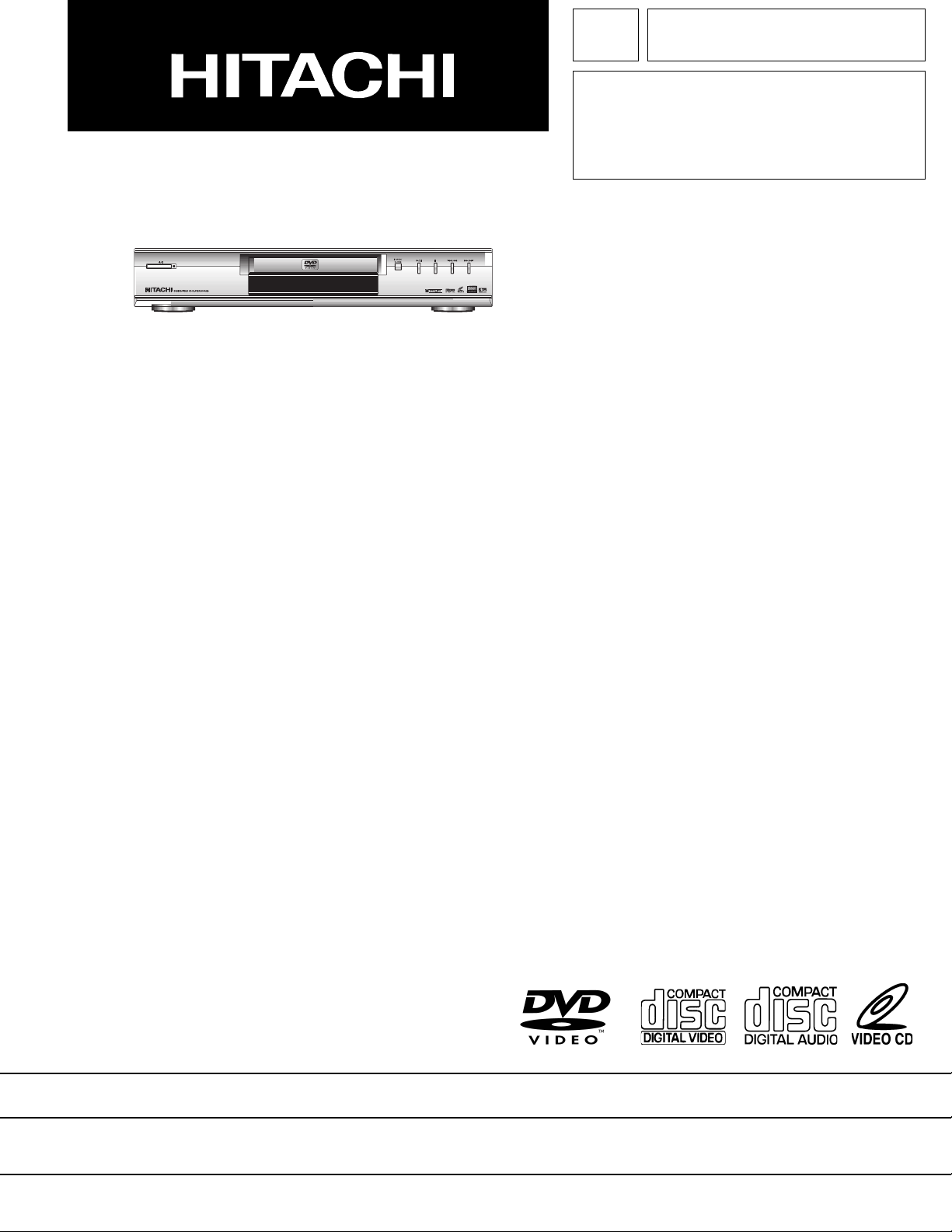
SERVICE MANUAL
TK No.9103E
DV-P415U
CONTENTS
1. Precautions
2. Product Specifications
3. Operating Instructions
4. Disassembly and Reassembly
5. Troubleshooting
6. Exploded Views
7. Replacement Parts List
8. Block Diagrams
9. PCB Diagrams
10. Wiring Diagram
11. Schematic Diagram
SPECIFICATIONS AND PARTS ARE SUBJECT TO CHANGE FOR IMPROVEMENT
DVD PLAYER
2001March
Digital Media Products Division, Tokai
Page 2
1-1
1. Precautions
1-1 Safety Precautions
1) Before returning an instrument to the customer,
always make a safety check of the entire
instrument, including, but not limited to, the
following items:
(1) Be sure that no built-in protective devices are
defective or have been defeated during servicing.
(1)Protective shields are provided to protect both
the technician and the customer. Correctly replace
all missing protective shields, including any
remove for servicing convenience.
(2)When reinstalling the chassis and/or other assembly in the cabinet, be sure to put back in place
all protective devices, including, but not limited to,
nonmetallic control knobs, insulating fish papers,
adjustment and compartment covers/shields, and
isolation resistor/capacitor networks. Do not
operate this instrument or permit it to be operated
without all protective devices correctly installed
and functioning.
(2) Be sure that there are no cabinet openings
through which adults or children might be able to
insert their fingers and contact a hazardous
voltage. Such openings include, but are not limited
to, excessively wide cabinet ventilation slots, and
an improperly fitted and/or incorrectly secured
cabinet back cover.
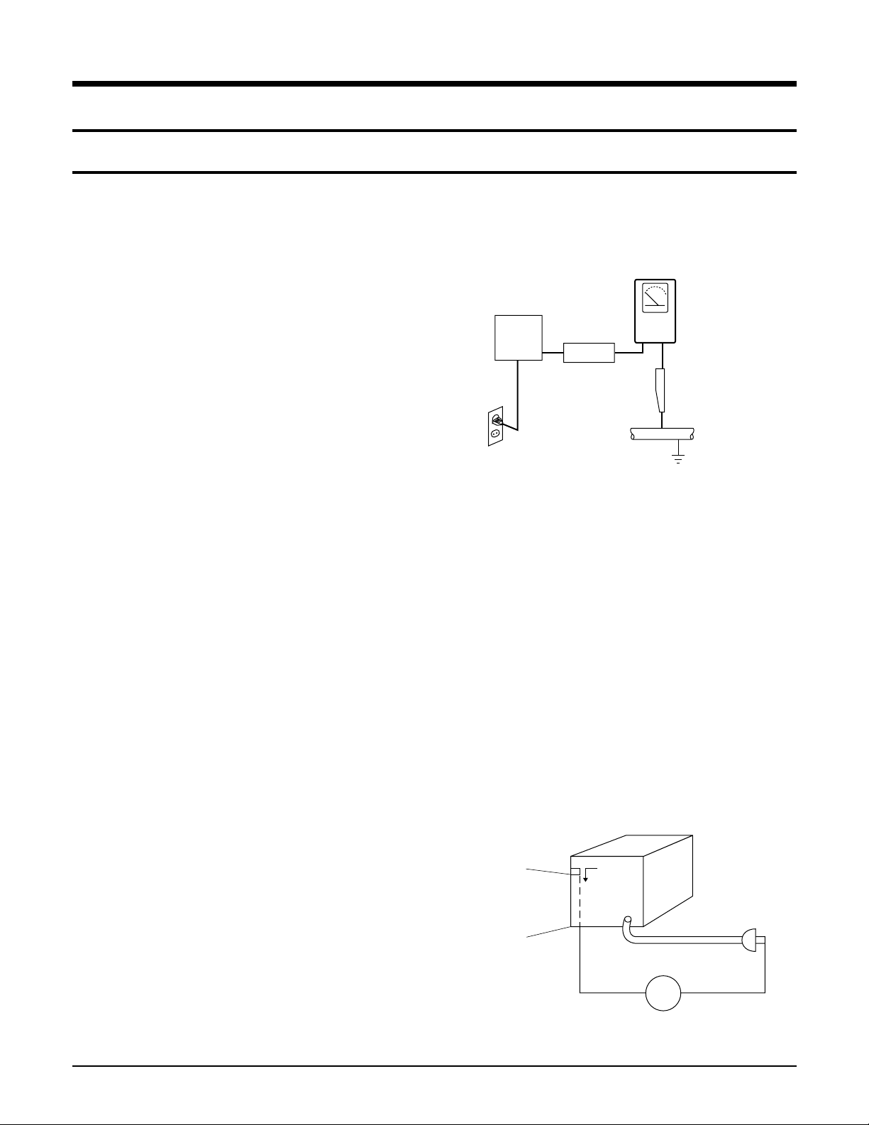
(3) Leakage Current Hot Check-With the instrument
completely reassembled, plug the AC line cord
directly into a 120V AC outlet. (Do not use a
isolation transformer during this test.) Use a
leakage current tester or a metering system that
complies with American National Standards
institute (ANSI) C101.1 Leakage Current for
Appliances and Underwriters Laboratories (UL)
1270 (40.7). With the instrument's AC switch first in
the ON position and then in the OFF position,
measure from a known earth ground (metal water
pipe, conduit, etc.) to all exposed metal parts of
the instrument (antennas, handle brackets, metal
cabinets, screwheads, metallic overlays, control
shafts, etc.), especially any exposed metal parts
that offer an electrical return path to the chassis.
Any current measured must not exceed 0.5mA.
Reverse the instrument power cord plug in the
outlet and repeat the test. See Fig. 1-1.
Any measurements not within the limits specified
herein indicate a potential shock hazard that must
be eliminated before returning the instrument to
the customer.
Fig. 1-1 AC Leakage Test
(4) Insulation Resistance Test Cold Check-(1) Unplug
the power supply cord and connect a jumper wire
between the two prongs of the plug. (2) Turn on the
power switch of the instrument. (3) Measure the
resistance with an ohmmeter between the
jumpered AC plug and all exposed metallic cabinet
parts on the instrument, such as screwheads,
antenna, control shafts, handle brackets, etc.
When an exposed metallic part has a return path
to the chassis, the reading should be between 1
and 5.2 megohm. When there is no return path to
the chassis, the reading must be infinite. If the
reading is not within the limits specified, there is
the possibility of a shock hazard, and the
instrument must be re-pared and rechecked before
it is returned to the customer. See Fig. 1-2.
Fig. 1-2 Insulation Resistance Test
DEVICE
UNDER
TEST
(READING SHOULD
NOT BE ABOVE
0.5mA)
LEAKAGE
CURRENT
TESTER
EARTH
GROUND
TEST ALL
EXPOSED METER
SURFACES
ALSO TEST WITH
PLUG REVERSED
(USING AC ADAPTER
PLUG AS REQUIRED)
2-WIRE CORD
Antenna
Terminal
Exposed
Melal Part
ohm
ohmmeter
Page 3

Precautions
1-2
2) Read and comply with all caution and safety related notes non or inside the cabinet, or on the
chassis.
3) Design Alteration Warning-Do not alter of add to
the mechanical or electrical design of this
instrument. Design alterations and additions,
including but not limited to, circuit modifications and
the addition of items such as auxiliary audio output
connections, might alter the safety characteristics
of this instrument and create a hazard to the user.
Any design alterations or additions will make you,
the service, responsible for personal injury or
property damage resulting therefrom.
4) Observe original lead dress. Take extra care to
assure correct lead dress in the following areas:
(1) near sharp edges, (2) near thermally hot parts
(be sure that leads and components do not touch
thermally hot parts), (3) the AC supply, (4) high
voltage, and (5) antenna wiring. Always inspect in
all areas for pinched, out-of-place, or frayed wiring,
Do not change spacing between a component and
the printed-circuit board. Check the AC power cord
for damage.
5) Components, parts, and/or wiring that appear to
have overheated or that are otherwise damaged
should be replaced with components, parts and/ or
wiring that meet original specifications.
Additionally, determine the cause of overheating
and/or damage and, if necessary, take corrective
action to remove any potential safety hazard.
6) Product Safety Notice-Some electrical and
mechanical parts have special safety-related
characteristics which are often not evident from
visual inspection, nor can the protection they give
necessarily be obtained by replacing them with
components rated for higher voltage, wattage, etc.
Parts that have special safety characteristics are
identified by shading, an ( )or a ( )on
schematics and parts lists. Use of a substitute
replacement that does not have the same safety
characteristics as the recommended replacement
part might created shock, fire and/or other hazards.
Product safety is under review continuously and
new instructions are issued whenever appropriate.
Page 4

Precautions
1-3
1-2 Servicing Precautions
CAUTION : Before servicing Instruments covered
by this service manual and its supplements, read and
follow the Safety Precautions section of this manual.
Note : If unforseen circument create conflict between
the following servicing precautions and any of the
safety precautions, always follow the safety
precautions. Remember: Safety First.
1-2-1 General Servicing Precautions
(1) a. Always unplug the instrument's AC power cord
from the AC power source before (1) re-moving
or reinstalling any component, circuit board,
module or any other instrument assembly, (2)
disconnecting any instrument electrical plug or
other electrical connection, (3) connecting a test
substitute in parallel with an electrolytic
capacitor in the instrument.
b.Do not defeat any plug/socket B+ voltage
interlocks with which instruments covered by this
service manual might be equipped.
c. Do not apply AC power to this instrument and
/or any of its electrical assemblies unless all
solid-state device heat sinks are correctly installed.
d. Always connect a test instrument's ground lead
to the instrument chassis ground before
connecting the test instrument positive lead.
Always remove the test instrument ground lead
last.
Note : Refer to the Safety Precautions section ground
lead last.
(2) The service precautions are indicated or printed
on the cabinet, chassis or components. When
servicing, follow the printed or indicated service
precautions and service materials.
(3) The components used in the unit have a specified
flame resistance and dielectric strength.
When replacing components, use components
which have the same ratings. Components ientified by shading, by( ) or by ( ) in the circuit
diagram are important for safety or for the
characteristics of the unit. Always replace them
with the exact replacement components.
(4) An insulation tube or tape is sometimes used and
some components are raised above the printed
wiring board for safety. The internal wiring is
sometimes clamped to prevent contact with
heating components. Install such elements as they
were.
(5) After servicing, always check that the removed
screws, components, and wiring have been installed correctly and that the portion around the
serviced part has not been damaged and so on.
Further, check the insulation between the blades
of the attachment plug and accessible conductive
parts.
1-2-2 Insulation Checking Procedure
Disconnect the attachment plug from the AC outlet
and turn the power ON. Connect the insulation resistance meter (500V) to the blades of the attachment
plug. The insulation resistance between each blade of
the attachment plug and accessible conductive
parts(see note) should be more than 1 Megohm.
Note : Accessible conductive parts include metal
panels, input terminals, earphone jacks, etc.
Page 5

Precautions
1-4
1-3 ESD Precautions
Electrostatically Sensitive Devices (ESD)
Some semiconductor (solid state) devices can be
damaged easily by static electricity.
Such components commonly are called Electrostatically Sensitive Devices(ESD). Examples of typical
ESD devices are integrated circuits and some fieldeffect transistors and semiconductor chip
components. The following techniques should be used
to help reduce the incidence of component damage
caused by static electricity.
(1) Immediately before handling any semiconductor
component or semiconductor-equipped assembly,
drain off any electrostatic charge on your body by
touching a known earth ground. Alternatively,
obtain and wear a commercially available
discharging wrist strap device, which should be
removed for potential shock reasons prior to
applying power to the unit under test.
(2) After removing an electrical assembly equipped
with ESD devices, place the assembly on a
conductive surface such as aluminum foil, to
prevent electrostatic charge buildup or exposure of
the assembly.
(3) Use only a grounded-tip soldering iron to solder or
unsolder ESD devices.
(4) Use only an anti-static solder removal devices.
Some solder removal devices not classified as
"anti-static" can generate electrical charges
sufficient to damage ESD devices.
(5) Do not use freon-propelled chemicals. These can
generate electrical charges sufficient to damage
ESD devices.
(6) Do not remove a replacement ESD device from its
protective package until immediately before your
are ready to install it.(Most replacement ESD
devices are packaged with leads electrically
shorted together by conductive foam, aluminum
foil or comparable conductive materials).
(7) Immediately before removing the protective ma-
terials from the leads of a replacement ESD
device, touch the protective material to the chassis
or circuit assembly into which the device will be
installed.
CAUTION : Be sure no power is applied to the ch-
assis or circuit, and observe all other safety
precautions.
(8) Min imi ze bodily motions when handling
unpackaged replacement ESD devices. (Otherwise
harmless motion such as the brushing together of
your clothes fabric or the lifting of your foot from a
carpeted floor can generate static electricity
sufficient to damage an ESD device).
Page 6
Precautions
1-5
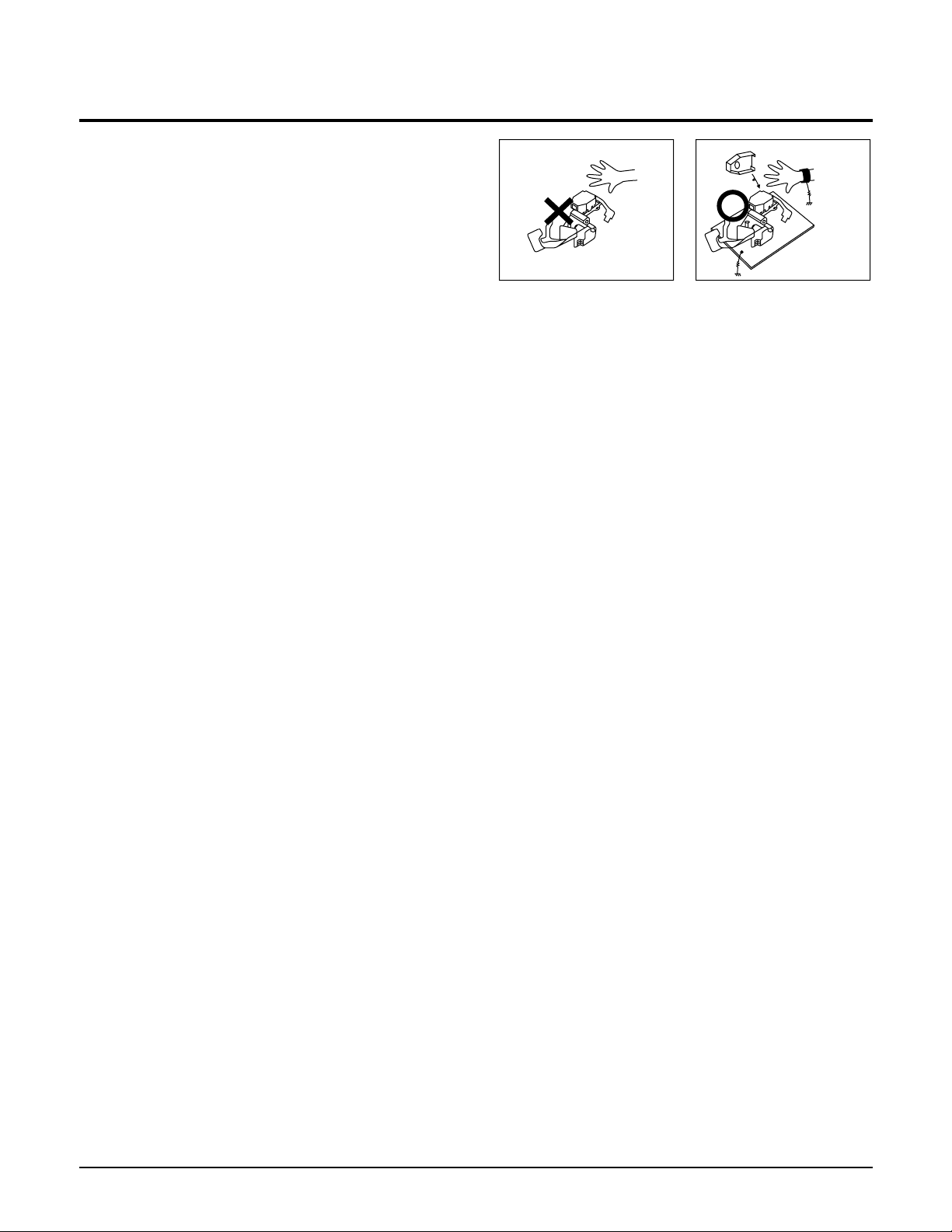
1-4 Handling the optical pick-up
The laser diode in the optical pick up may suffer
electrostatic breakdown because of potential static
electricity from clothing and your body.
The following method is recommended.
(1) Place a conductive sheet on the work bench (The
black sheet used for wrapping repair parts.)
(2) Place the set on the conductive sheet so that the
chassis is grounded to the sheet.
(3) Place your hands on the conductive sheet(This
gives them the same ground as the sheet.)
(4) Remove the optical pick up block
(5) Perform work on top of the conductive sheet. Be
careful not to let your clothes or any other static
sources to touch the unit.
♦ Be sure to put on a wrist strap grounded to the
sheet.
♦ Be sure to lay a conductive sheet made of copper
etc. Which is grounded to the table.
Fig.1-3
(6) Short the short terminal on the PCB, which is in-
side the Pick-Up ASS'Y, before replacing the PickUp. (The short terminal is shorted when the PickUp Ass'y is being lifted or moved.)
(7) After replacing the Pick-up, open the short
terminal on the PCB.
THE UNIT
WRIST-STRAP
FOR GROUNDING
1M
1M
CONDUCTIVE SHEET
Page 7
Precautions
1-6
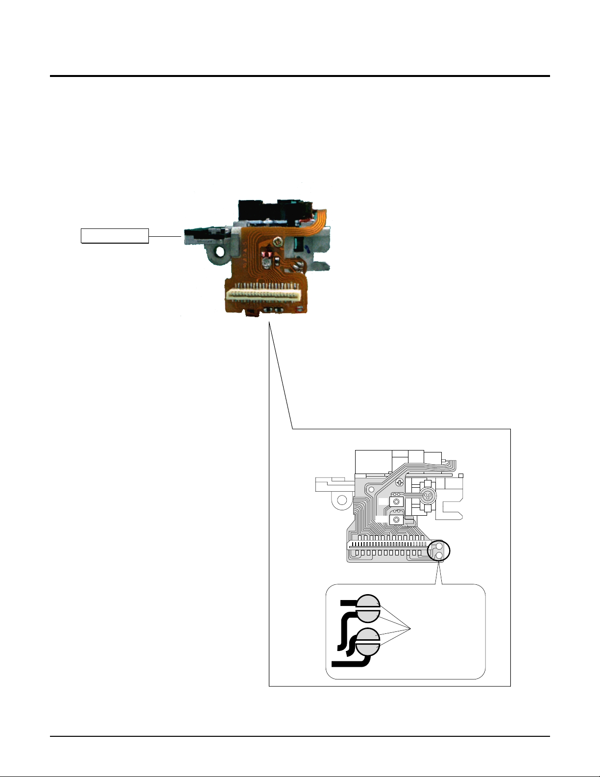
1-5-1 Disassembly
1) Remove the power code.
2) Disassemble the Deck-Assy.
3) Solder land 4 points short on Pick-up.(See Fig. 1-4)
4) Disassembly the Pick-up.
1-5-2 Assembly
1) Replace the Pick-up.
2) Remove the soldering 4 points on Pick-up.
3) Reassemble the Deck-Assy.
PICK-UP ASS'Y
CD
DVD
SOLDER LAND
4 POINTS SHORT
Note : If the assembly and disassembly are not done in correct sequence, the Pick-up may be damaged.
Fig. 1-4
1-5 Pick-up disassembly and reassembly
Page 8
2-1
2. Product Specifications
Power Requirements AC 120V, 60Hz
Power Consumption 15W
GENERAL
Weight 2.7kg
Dimensions W 430mm X D 240mm X H 79mm
Operating Temperature Range +5°C ~ +35°C
Operating Humidity Range 10% to 75%
DVD Reading Speed : 3.49 m/s
(Digital Versatile Disc) Approx. Play Time (Single Sided, Single Layer Disc) : 135 min.
CD : 12Cm Reading Speed : 1.2 to 1.4 m/s
DISC
(Compact Disc) Maximum Play Time : 74min.
CD : 8Cm Reading Speed : 1.2 to 1.4 m/s
(Compact Disc) Maximum Play Time : 20min.
VCD : 12Cm
Reading Speed : 1.2 to 1.4 m/s
Maximum Play Time : 74min. (Video + Audio)
Composite Video 1 channel : 1.0Vp-p (75ohm load)
Y : 1.0Vp-p (75ohm load)
Video Output
Component Video Pr : 0.70Vp-p (75ohm load)
Pb : 0.70Vp-p (75ohm load)
S-Video
Luminance Signal : 1Vp-p (75ohm load)
Chrominance Signal : 0.286Vp-p (75ohm load)
2 Channel L (1/L), R (2/R)
* Frequency Response
48kHz Sampling : 4Hz to 22kHz
Audio Output
96kHz Sampling : 4Hz to 44kHz
* S/N Ratio 110dB
* Dynamic Range 100dB
* Total Harmonic Distortion 0.004%
* : Nominal specification
Page 9
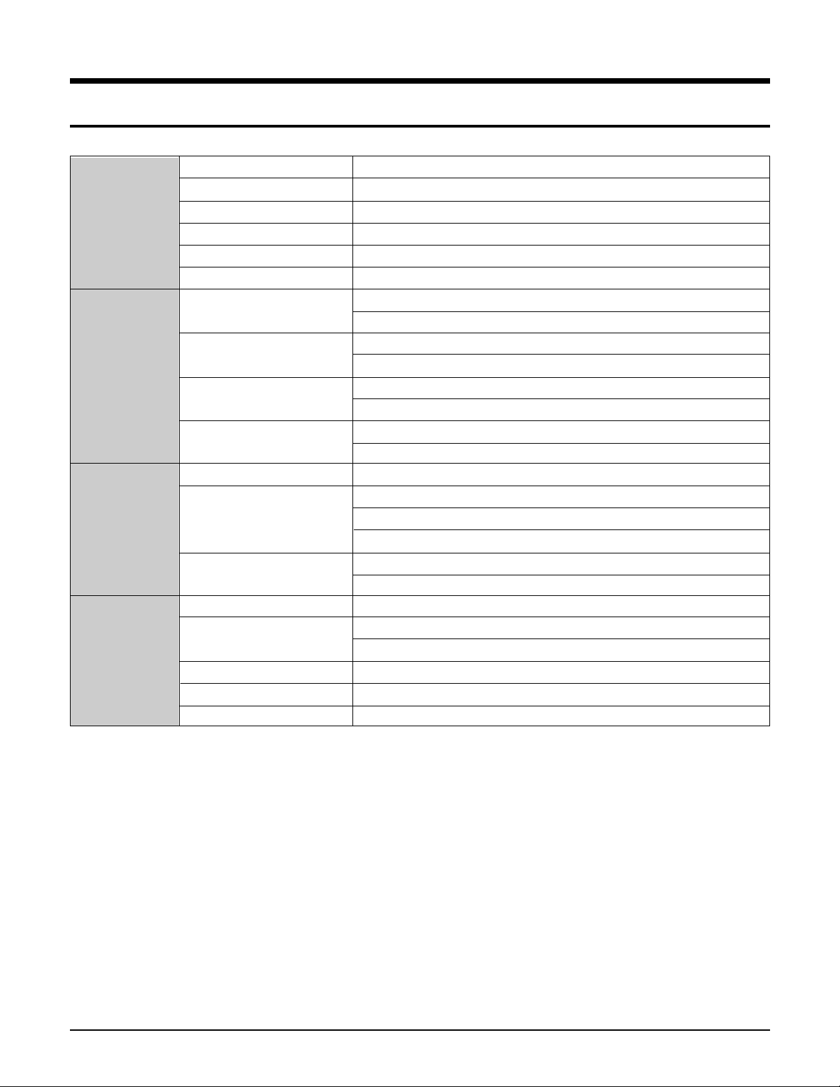
3-1
3. Operating Instructions
14
POWER/STANDBY
When the unit is first plugged in, the indicator lights. When POWER/STANDBY is
pressed, the lamp goes out and the player is turned on.
DISC TRAY
••Press OPEN/CLOSE to open and close the disc tray.
DISPLAY
• Operation indicators are displayed here.
OPEN/CLOSE
• Press to open and close the disc tray.
(PLAY/PAUSE)
• Begin or pause disc play.
(STOP)
• Stops disc play.
(SKIP/SEARCH)
• Use to skip a scene or music.
• If this button is held down for approx. two seconds, it will switch to the search button:
Thereafter, each time the button is pressed, the search speed will switch to 2X, 4X,
8X, 16X, 32X, 128X, after which SKIP will be restored.
Description-Front Panel
Front Panel Controls
15
You can now select different viewing points of the scene recorded by different
cameras (Multi Angle).
Disc type indicators
Reverse playback / Pause / Forward playback
Lights when 3D sound is turned on.
DVD : Title number
DVD : Chapter number.
Video/Audio CD : Track number
Repeat play mode
Linear PCM audio output
Dolby Digital audio output
DTS (Digital Theater System) audio output(Digital only)
MPEG-2 Audio output
Displays various messages concerning operations such as PLAY, STOP, LOAD,
RANDOM, ...
no DISC : No disc loaded.
OPEN : The disc tray is open.
LOAD : Player is loading disc information.
Front Panel Display
Front Panel Display
Œ
´
ˇ
¨
ˆ
Ø
∏
”
’
˝
Ô
Ò
POWER/STANDBY
Page 10
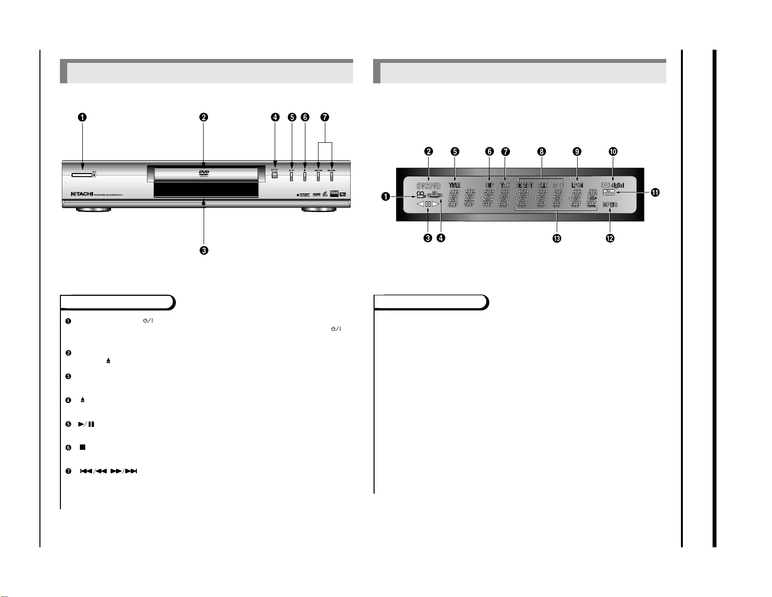
Operating Instructions
3-2
How to handle the remote control
16
Tour of the Remote Control
• Operate the remote control within the following area, in a straight line from the signal
detecting eye of the player and an angle of 30°.
30
Aprox.7metros
30
30
30
17
POWER/STANDBY Button
• Turns the player on and off.
A-B REPEAT Button
• Marks a segment to repeat between A and B.
REPEAT Button
•Allows you to repeat play a title, chapter, track, or disc.
MODE Button
• Allows you to program a specific order.
RETURN Button
• Returns to a previous menu.
ANGLE Button
•Accesses various camera angles on a disc.
SUBTITLE Button
•Accesses various subtitles on a disc.
MENU Button
• Brings up the Menu on a disc.
ENTER/DIRECTION Button (UP/DOWN or LEFT/RIGHT Button)
DISC NAVIGATION Button
• To view the first picture of each chapter(DVD) or track(VCD).
STEP Button
•Advances playback one frame at a time.
STOP Button
• To stop playback.
SEARCH Buttons
•Allows you to search forward/backward through a disc.
TV POWER Button
• To turn the TV on and off.
VIDEO/TV Button
• To select the input: VIDEO (DVD player) or TV.
SURROUND Button
• To activate the 3D sound.
BOOKMARK Button
• To rapidly return to a location of disc.
OPEN/CLOSE Button
• To open or close the disc tray.
NUMBER Buttons
ZOOM Button
• To magnify part of picture.
CLEAR Button
• Removes menus or status displays from the screen.
DISPLAY Button
• Displays the current disc mode.
AUDIO Button
•Accesses various audio functions on a disc.
TOP MENU Button
• Brings up the Top Menu on a disc.
SETUP Button
• Brings up the DVD player’s Setup menu.
SKIP Buttons
• Skip the, Chapter, or Track.
PLAY/PAUSE Button
• Begin/Pause disc play.
VOL Buttons
• To adjust the TV volume.
CH Buttons
• To switch TV channels.
Tour of the Remote Control
DVD Function Buttons
DV-RM410
Œ
´
ˇ
¨
ˆ
Ø
∏
”
’
˝
Ô
Ò
Ú
Æ
ı
˜
¯
˘
¿
¸
˛
◊
±
≠
–
—
÷
®
Page 11
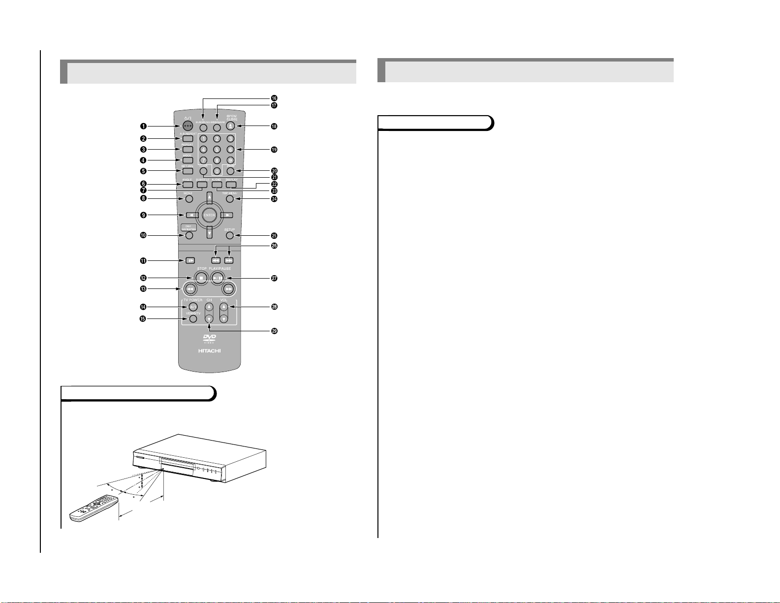
Operating Instructions
3-3
22
DIGITALAUDIO OUT JACK
• Use either an optical or coaxial digital
cable to connect to a compatible
Dolby Digital receiver. Use to connect
to an A/V Amplifier that contains a
Dolby Digital decoder or DTS
decoder.
MIXED AUDIO OUT JACKS
• Connect to the Audio input jacks of
your television, audio/video receiver.
VIDEO OUT JACK
• Use a video cable to connect one of
the jack to the Video input on your
television.
S-VIDEO OUT JACK
• Use the S-Video cable to connect this
jack to the S-Video jack on your
television for a higher quality picture.
The S-Video must be selected in the
VIDEO OUT SELECT switch.
COMPONENT VIDEO OUT JACKS
• Use these jacks if you have a TV with
Component Video in jacks. These
jacks provide Pr, Pb and Y video.
Along with S-Video, Component Video
provides the best picture quality. The
Y, Pb, Pr must be selected in the
VIDEO OUT SELECT switch.
VIDEO OUT SELECT switch
• Use the switch to set video out.
• If the Y, Pb or Pr is selected, the S-
Video may not work.
• If the S-Video is selected, the Y, Pb or
Pr may not work.
Description-Rear Panel
Rear Panel
COMPONENT VIDEO OUT
YPr
Pb
VIDEO OUT S-VIDEO OUT
MIXED AUDIO OUT
RL
OPTICAL COAXIAL
DIGITAL AUDIO OUT
S-VIDEO
Y,P b ,P r
VIDEO OUT
SELECT
Œ
´
ˇ
¨
ˆ
Ø
Page 12
4-1
4. Disassembly and Reassembly
4-1 Cabinet and PCB
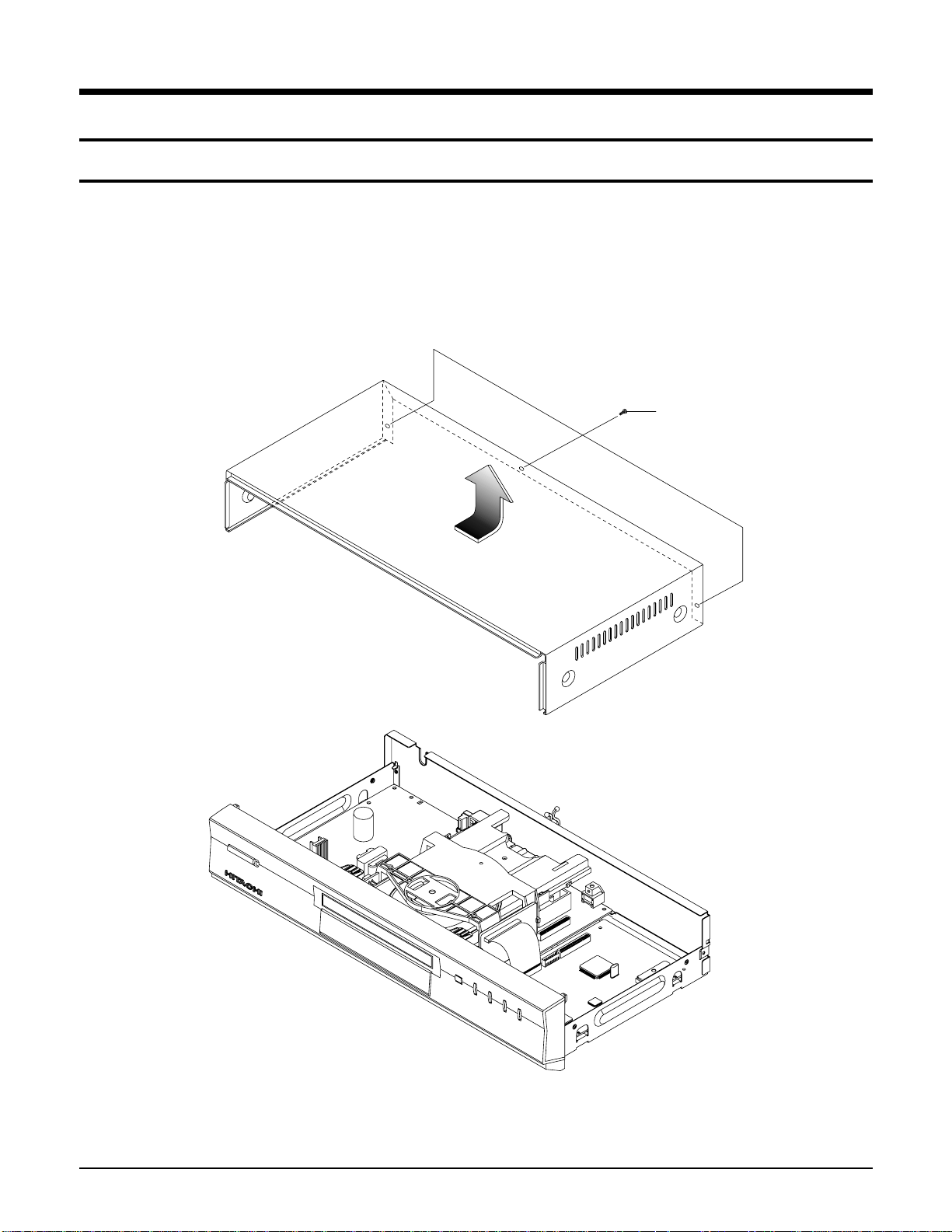
4-1-1 Top Cabinet Removal
1) Remove 3 Screws Πon the back Top Cabinet.
2) Lift up the Top Cabinet in direction of arrow.
Π3 SCREWS
Fig. 4-1 Top Cabinet Removal
Note : Reassembly in reverse order.
Page 13
4-2
Disassembly and Reaasembly
4-1-2 Door-Tray Removal
1) Supply power and open Tray Œ.
2) Disassemble the Door-Tray ´ in direction of arrow "A".
3) Close Tray Πand power off.
Note : If Tray Œ doesn't open, insert a Screw driver ¨ into the Emergency hole ˇ (as shown in detailed drawing)
and then push it in the direction of arrow "B". Open Tray manually.
ΠTRAY
´ DOOR-TRAY
"A"
<Side View>
ˇ EMERGENCY HOLE
¨ SCREW DRIVER
"B"
Fig. 4-2 Door-Tray Removal
Page 14
Disassembly and Reaasembly
4-3
Fig. 4-3 Ass'y Front-Cabinet Removal
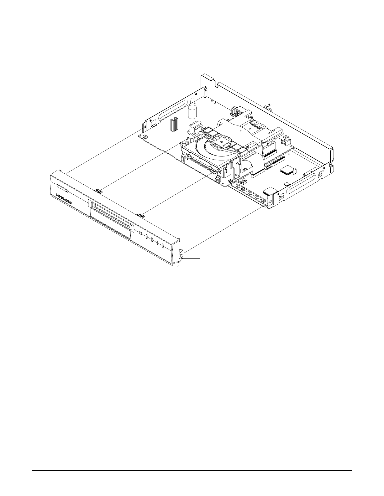
4-1-3 Ass'y Front-Cabinet Removal
1) Remove Ass'y Front-Cabinet Œ.
ΠASS'Y FRONT-CABINET
Page 15
4-4
Disassembly and Reaasembly
4-1-4 Ass'y Deck Removal
1) Disconnect Flat-Cable,Connect-Wire from DCN1, DCN2 on Main PCB.
2) Remove 3 Screws Πfrom the Ass'y Deck and lift it up.
Fig. 4-4 Ass'y Deck Removal
Π3 SCREWS
DECK-ASS'Y
CONNECT-WIRE
FLAT-CABLE
MAIN PCB
DCN1
DCN2
Page 16

Disassembly and Reaasembly
4-5
Fig. 4-5 Main PCB, Jack PCB Removal
4-1-5 Main PCB, Jack PCB Removal
1) Remove 2 Screws Œ and lift up the Jack PCB ´.
2) Remove 3 Screws ˇ and lift up the Main PCB ¨.
Π2 SCREWS
´ JACK PCB
ˇ 3 SCREWS
¨ MAIN PCB
Page 17

4-6
Disassembly and Reaasembly
4-2 PCB Location
Fig. 4-6 PCB Location
Page 18

Disassembly and Reaasembly
4-7
4-3 Connector Diagram
Fig. 4-7 Connector Diagram
DECK-ASS'Y
JACK PCB
˝
CT5
ˇ
CT4
’
”
¨
´
DECK PCB
CT1
Œ
CT2
CT3
Ø
ˆ
∏
MAIN PCB
NO. CONNECTOR NO. DIRECTION CONNECTOR NO. NO.
Œ FLAT-CABLE DECK PCB MAIN PCB DCN1 ´
ˇ
CONNECT-WIRE
(HCN1) HOUSING PCB MAIN PCB DCN2 ¨
ˆ CN8 MAIN PCB JACK PCB DCN1 Ø
∏ PCN1 MAIN PCB JACK PCB PCNS1 ”
’ FCN1 MAIN PCB JACK PCB CN2-S ˝
CT1
CT2
CT3
CT4
CT5
Page 19

4-8
Disassembly and Reaasembly
4-4 Deck
4-4-1 Tray Disc Removal
1) Insert a Screw Driver Œ into Emergency Hole ´ and push the Slider Housing ˇ in the direction arrow "A".
2) When the Tray Disc ¨ comes out a little, pull it in the direction arrow "B" by hand.
3) Pull the Tray Disc ¨ to disassemble , while simultaneously pushing 2 Stoppers ˆ (left, right) in the direction
arrow "C", "D".
Fig. 4-8 Tray Disc Removal
¨ TRAY DISC
ˆ STOPPER
"B"
"C"
"D"
ˆ STOPPER
ˇ SLIDER HOUSING
"A"
ΠSCREW DRIVER
´ EMERGENCY HOLE
Page 20

Disassembly and Reaasembly
4-9
4-4-2 Ass'y P/U Deck Removal
1) Disconnect DCN2 Œ, DCN3 ´.
2) Lift down the Assy P/U Deck ˇ while simultaneously pushing 2 Hooks ¨, ˆ in the direction of arrow
"A", "B".
Fig. 4-9 Ass'y P/U Deck Removal
¨ HOOK
"A"
ˆ HOOK
"B"
<Assembly Point>
SLIDER HOUSING
ΠDCN2
´ DCN3
ˇ ASSY- P/U DECK
Page 21

4-10
Disassembly and Reaasembly
4-4-3 Housing Ass'y Removal
1) Remove Belt Œ.
2) Push the Hook ´ in the direction arrow "A" and lift up Pulley Gear ˇ.
3) Push the Slider Housing ˆ in the direction arrow "B" and lift up the Gear Tray ¨.
4) Lift up the Slider Housing ˆ.
5) Remove the soldering Ø of 2 points (Red, Black).
6) Remove 2 Screws ∏ and lift down the Motor Load Ass'y ”.
7) Push the 3 Hooks ’ bottom side in the direction arrow "C" and lift up the Housing PCB ˝.
8) Push the Hooks Ô and remove Deck PCB .
Fig. 4-10 Housing Ass'y Removal
"B"
∏ 2 SCREWS
´ HOOK
"A"
ˆ SLIDER HOUSING
¨ GEAR TRAY
ˇ PULLEY GEAR
ΠBELT
” MOTOR LOAD ASSY
"C"
˝ HOUSING PCB
Ô HOOK
DECK PCB
Ø SOLDERING
"C"
"C"
’ 3 HOOKS
<Bottom Side>
Page 22

Disassembly and Reaasembly
4-11
4-4-4 Sub Chassis Removal
1) Remove the Soldering of Motor Feed (+, - wire) Œ.
2) Remove the 4 Screws ´.
3) Lift up the Ass'y Brkt Deck ˇ.
Fig. 4-11 Sub Chassis Removal
´ 4 SCREWS
ˇ ASSY-BRAK DECK
ΠSOLDERING OF
MOTOR FEED (+, - WIRE)
+
Page 23

4-12
Disassembly and Reaasembly
4-4-5 Ass'y Brkt Deck Removal
1) Remove Washer Œ.
2) Remove Gear Feed B ´ , Gear Feed A ˇ.
3) Remove 2 Screws ¨.
4) Remove Shaft Pick-Up ˆ and Pick-Up Assy Ø.
5) Remove 1 Screw ∏.
6) Remove 2 Screws ”.
7) Remove 3 Spring Spindle ’ and Motor Spindle Ass'y ˝.
Fig. 4-12 Ass'y Brkt Deck Removal
˝ MOTOR SPINDLE
’ SPRING SPINDLE
ˆ SHAFT PICK-UP
Ø PICK-UP ASS'Y
¨ 2 SCREW
ΠWASHER
´ GEAR FEED B
∏ 1 SCREW
” 2 SCREWS
ˇ GEAR FEED A
Page 24

5-1
5. Troubleshooting
No Disc recognition
LD is outputted
from object lens at
play key input?
No focus incoming and
no disc occurs.
Yes
No
B
A
No focus incoming
A
FE in SIC1-25
is within specified range?
Yes
SIC3-26, 27 output
are normal?
Yes
Check open state from
SIC3 to pick-up.
No
No
Check RIC1 and A, B, C, D input.
Check SIC3.
Page 25

Troubleshooting
5-2
No pick-up home positing
SLD, SIC1-34
output is normal?
Yes
LED+, SLED-
SIC3-32, 33 output are
normal?
Yes
Check the Sled Motor and connection
No
No
Check MIC1
Check SIC3
NO LD CD ON
B
RIC1-21 is 5V?
Yes
Divide RQ1 emitter terminal
voltage and 5V real voltage
difference into 10ohm.
Yes
Current exceeds 0.1A?
Yes
No
No
Check MIC1
Open check in related circuit.
LD out pick-up replace.
Page 26

Troubleshooting
5-3
No Search Operation
FINE SEEK Check
MIRR, SIC1-157
output is normal?
Yes
Actual velocity occurs
at SIC1-34 terminal?
Yes
Actual velocity occurs
at SIC4-32, 33 terminal?
Yes
No
No
No
RFAGCO, RIC1-72
output level is normal?
Yes
Check RIC1 peripheral circuit.
Check SIC1 peripheral circuit.
Check SIC3 peripheral circuit.
No
Check pick-up.
FINE SEEK MIRR
signal (RIC1-46) is missing?
No
TZCO signal
(SIC1-24) is occurs?
Yes
Track incomming is
delayed?
Yes
TE is within
2V and 3V?
Yes
Pick-up transfer smooth.
Yes
No
Check RIC1 Peripheral curcuit.
No
Check SIC1 Peripheral curcuit.
No
Time out due to many jump counts.
No
SIC1-33 output
is normal?
SIC3-28, 29
terminal outputs are
normal?
Yes
No
Check RIC1-26 terminal.
No
TE occurs in
search range?
Yes
See "Fine Seek Check"
No
Focus On?
No
A
Yes
Check MECHA.
Yes
Check SIC3 peripheral circuit.
Check SIC1 peripheral circuit.
Check DCN1 and pick-up.
Page 27

Troubleshooting
5-4
Abnormal rotation of
disc motor
Input of RF signal
is normal? (SIC1-15)
Yes
SPD output is normal?
(SIC1-35)
Yes
SIC3-2 output (FG)
is normal?
No
No
After resoldering SIC1.
Check path to RIC1 and SIC1.
No
Check SIC3 soldering and power.
RIC1-71 output
is normal?
Yes
RIC1-70 output
are normal?
Yes
No
Check RIC1 peripheral
circuit and A, B, C, D.
No
Check RIC1 soldering and power.
No Tray open/close
MIC1-6, 8 is
Open ; "L", "L" ?
Close ; "H", "H"?
Yes
Check SIC3-35, 36
output at open/close
Yes
Check signal line state from
SIC3-35, 36 to tray motor.
No
No
Micom (MIC1) error.
Check SIC3.
Yes
SIC3-9 signal
MON is "H" ?
Yes
Check or replace disc motor.
No
Check SIC1, MIC1.
Page 28

Troubleshooting
5-5
CD/VCD/DVD L/R output error
(Mixed Audio output)
Digital output error
Normal DATA 0 is
input in AIC1-3?
Yes
Analog output of
AIC1-9, 10, 11, 12 is
normal?
Yes
AOP1-1, 7 output
is normal?
Yes
Base terminal level
of AQ1, AQ3
are "L"?
Yes
No
No
No
No
Check ZIC1-121 output.
Check ZIC1-125
(CD/VCD ; 16.9344MHz,
DVD ; 18.432MHz)
Check AOP1 peripheral circuit.
Check FIC1-47 mute.
Output in ZIC1-127 is normal?
Yes
Output in
AIC3-6, 8, 10 is
normal?
Yes
Check AVJ4, ACJ5 peripheral
soldering shot.
No
No
Check ZIC1 peripheral circuit.
Check AIC3.
Check AVJ2 peripheral
soldering shot.
Page 29

Troubleshooting
5-6
No Power
(Standby LED OFF)
PFD01 error?
No
PDS01 voltage
is missing?
Yes
PICF1 Drain (pin 1)
voltage is missing?
Yes
Voltage exists in
PICF1-4?
Yes
Yes
No
No
No
Replace fuse.
Check PRF10.
Check 2d voltage.
Check PRF11 ~ PRF14.
CVBS output error
D
Pin of VDD_2.5 &
VDD-3.3 in Zic1 has
normal level?
Yes
27MHz clock
input is normal at
pin 159 in ZIC1?
Yes
Analog output
is normal at pin 133
in ZIC1?
Yes
Analog signals are
inputted normally
pin 2 in VIC1?
Yes
Power is
normal at pin 1, 28
in VIC1?
Yes
Pin 7 in VIC1
is in high stste?
Yes
No
No
No
No
No
No
Check the connection between
pin 1 in PCNS1 and pin 3 in ZIC5.
Check the connection between
pin 6 in ZIC4 and pin 129 in ZIC1.
Check the soldering of ZIC1.
Check the connection netween
pin 133 in ZIC1 and VIC1.
Check the connection betwen
VIC1 and PICS4-2.
Check the connection between
PICS4-2 and pin 1 in VIC1.
Pulse is missing
in PICF1-5?
No
Replace PICF1.
Yes
Replace PICF1.
Check feed back.
Peak to peak
voltage level of pin 27
in VIC1 is 2V?
Yes
Video signal of
about 1V appears at
output jack?
Yes
Check the RCA cable.
No
No
Check the soldering of VIC1.
Check the connection between
VIC1 and output jack.
Page 30

Troubleshooting
5-7
S-Video output error
Y/Pr/Pb output error
VSW1 video select
switch is up position?
Yes
VR121 of VSW1
is high state?
Yes
Pin 38 in FIC1
is high state?
Yes
D
No
No
No
Move the select switch to up position.
Check the soldering of VSW1.
Check the connection between
pin 38 in FIC1 and VR121.
VSW1 video select
switch is down position?
Yes
VR121 of VSW1
is low state?
Yes
Pin 38 in FIC1
is high state?
Yes
D
No
No
No
Move the select switch to down position.
Check the soldering of VSW1.
Check the connection between
pin 38 in FIC1 and VR121.
Page 31

6-1
6. Exploded View
6-1 Cabinet Assembly - - - - - - - - - - - - - - - - - - - - - - - - - - - - - - - -
6-2 Deck Assembly - - - - - - - - - - - - - - - - - - - - - - - - - - - - - - - - - -
Page
6-2
6-3
Page 32

Exploded Views
6-2
6-1 Cabinet Assembly
104
001
MAIN P.C.B
102
109
106
108
108
CN1B
101
002
JACK P.C.B
103
105
Page 33

6-3
Exploded Views
6-2 Deck Assembly
H105
DCN1A
H104
H207
H200
H211
H210
Page 34

MECHINISM SECTION
101 TS16461 MECHA ASSY(DVD)
102 TE13371 CORD,POWER
103 TJ14994 PANEL,FRONT
104 TJ15002 COVER,TOP
105 TJ15091 DOOR ASSY
106 TJ15021 PANEL,REAR
108 TJ15041 FOOT,FRONT
109 TJ15051 HOLDER,CORD
H104 TS16341 MOTOR,LOAD
H105 TJ15031 BELT,PUULEY
H200 TS16371 DECK,BRACKET
H207 TS16351 MOTOR,SPINDLE
H210 TS16361 MOTOR,FEED
H211 TS16491 PICK UP ASSY
001 TS16441 PWB ASSY MAIN
002 TS16451 PWB ASSY JACK
ACCESSORIES
802 TS16332 REMOTE HAND SET
803 TE13361 CABLE,AV
PCD02 TA14331 CERAMIC DISC 3.3nF 400V
PCD03 TA14311 CERAMIC DISC 3.3nF
PCR01 TA14301 CERAMIC DISC 10nF 400V
PCS03 TA14341 CERAMIC DISC 100pF 400V
PEF10 TA14291 CAPACITOR 150uF 200V
AD54 TC11651 DIODE 1N4148
PDS01 TC11631 DIODE 1T5
PDS02 TC11631 DIODE 1T5
PDS03 TC11631 DIODE 1T5
PDS04 TC11631 DIODE 1T5
PDS11 TC11661 DIODE UF4007
AIC1 TC11751 IC AK4382VT
AIC3 TC11481 IC M74HCU04
AOP1 TC11511 IC 4560
FIC1 TC11921 IC UPD780232GC-033
FIC2 TC11541 IC 7545
FIC4 TC11791 MODULE,REMOCON
MIC1 TC11931 IC 91C219
MIC2 TC11682 EPROM
MIC3 TC11941 IC 15M256
MIC4 TC11681 IC 24C021
MIC5 TC11351 IC TC7S08F
MIC6 TC11691 IC 7S32
MIC7 TC11401 IC 7SET00
PIC1 TC11701 IC MM1563
PICS1 TC11591 PHOTO COUPLER PC123
PICS2 TC11581 IC KA431Z
PICS3 TC11551 IC 7908
PICS4 TC11561 IC 78R08
PICS5 TC11951 IC 3RF23
RIC1 TC11711 IC S5L1462A
SIC1 TC11721 IC KS1454
SIC2 TC11731 IC 416C256
SIC3 TC11441 IC KA3017
SIC4 TC11351 IC TC7S08F
VIC1 TC11771 IC 1540
ZIC1 TC11461 IC ZIVA4.1
ZIC2 TC11981 IC 638165
ZIC4 TC11481 IC M74HCU04
PQR11 TC11611 SEMICONDUCTOR C5039F
PVA1 TC11641 SOMICONDUCTOR SVC471D
SY1 TE13881 CRYSTAL 33.8688MHZ
ZY1 TE13891 CRYSTAL 27HMZ
MY1 TE14351 CRYSTAL 20HMZ
FY1 TE13901 RESONATOR 5MHZ
PTD1 TA14191 TRANSFORMER
AVJ1 TE13931 JACK
AVJ2 TE13941 JACK
AVJ4 TE14191 JACK
AVJ5 TE14331 CONNECTOR
7-1
7. Replacement Parts List
7-1. MECHINICAL PARTS LIST 7-2.ELECTRICAL PARTS LIST
SYMBOL
NO
P-NO
DESCRIPTION
SYMBOL
NO
P-NO
DESCRIPTION
Page 35

SVJ1 TE13951 JACK
CN1B TE14001 CONNECTOR
CN8 TE13381 CONNECTOR(35P)
PCNS2 TE14291 CONNECTOR
PFD01 TE13401 FUSE
PICS6 TE13911 ICP-N25
PICS7 TE13911 ICP-N25
PLS01 TA14201 FILTER,LINE
VFD1 TE13921 DISPLAY
SW1 TE13981 SWITCH
SW2 TE14521 SWITCH
HSW1 TE14021 SWITCH
VSW1 TE13971 SWITCH,SLID
7-2
Replacement Parts List
SYMBOL
NO
P-NO
DESCRIPTION
SYMBOL
NO
P-NO
DESCRIPTION
Page 36

8-1
8. Block Diagram
DECK ASS'Y (DP-7)
SIC3
(KA3017)
Actuator & Motor Driver
Spindle/Sled/Tray Motor Pick-up & I/V Amp
SIC2 4M DRAM
ZIC2 SDRAM
MIC4 2K EEPROM
Remote Control FLT Display
MIC2 8M EPROM
Post Filter
Coaxial
Yout
Cout
SIC1
(S5L1454A)
Servo + DSP
RIC1
(S5L1462A)
RF Amp & DPD
MIC1
(TMP91C219F)
Main Controller
FIC1
(uPD780232)
Front Controller
ZIC1 (ZiVA-4.1)
A/V Decoder
CVBS
R/Pr
B/Pb
G/Y
Lt
Rt
Post
Filter
Optical
A/V
Decoder
AC3 &
MPEG 5.1
Video
Encoder
(4DAC)
AUDIO
DSP
CSS
INPUT
FIFO
&
DEMUX
AIC1 (AK4382)
2-CH Audio DAC
Down-L/R
Compo
Post Filter
Y/B/Pb
Post Filter
C/R/Pr
Post Filter
Comp/G/Y
IEC958/1937
VIC1
(MM1540)
MIC3 1M SDRAM
Page 37

9-1
9. PCB Diagrams
9-2
9-3
9-4
9-4
9-1 Main - - - - - - - - - - - - - - - - - - - - - - - - - - - - - - - - - - - - - - - -
9-2 Jack - - - - - - - - - - - - - - - - - - - - - - - - - - - - - - - - - - - - - - - -
9-3 Deck - - - - - - - - - - - - - - - - - - - - - - - - - - - - - - - - - - - - - - - -
9-4 Housing - - - - - - - - - - - - - - - - - - - - - - - - - - - - - - - - - - - - - -
Page 38

PCB Diagrams
9-2
9-1 Main
COMPONENT
SOLDER SIDE
Page 39

PCB Diagrams
9-3
9-2 Jack
Page 40

PCB Diagrams
9-4
9-4 Housing9-3 Deck
Page 41

10-1
10. Wiring Diagram
Page 42

11. Schematic Diagrams
Block Identification of PCB
Main PCB (Component Side)Main PCB (Component Side)
Jack PCB (Conductor Side)Jack PCB (Conductor Side)
T15M256A
M27C801
PIC1
MM1563
11-1 Power - - - - - - - - - - - - - - - - - - - - - - - - - - - - - - - - - - - - - -
11-2 AV-Decoder/Main-Micom/Key - - - - - - - - - - - - - - - - - - - - - -
11-3 Servo - - - - - - - - - - - - - - - - - - - - - - - - - - - - - - - - - - - - - - -
11-4 Video - - - - - - - - - - - - - - - - - - - - - - - - - - - - - - - - - - - - - - -
11-5 Audio - - - - - - - - - - - - - - - - - - - - - - - - - - - - - - - - - - - - - - -
11-6 Front-Micom/VFD Display - - - - - - - - - - - - - - - - - - - - - - - - -
11-7 Deck - - - - - - - - - - - - - - - - - - - - - - - - - - - - - - - - - - - - - - -
11-2
11-3
11-4
11-5
11-6
11-7
11-8
11-1
Page 43

Schematic Diagrams
11-1 Power
PICS6
ICP-N25
PICS7
ICP-N25
11-2
Page 44

11-2 AV-Decoder/Main-Micom/Key
Schematic Diagrams
M27C801
T15M256A
11-3
Page 45

Schematic Diagrams
11-3 Servo
S5L1462A
S5L1454A
11-4
Page 46

11-4 Video
Schematic Diagrams
11-5
Page 47

Schematic Diagrams
11-5 Audio
11-6
Page 48

11-6 Front-Micom/VFD Display
Schematic Diagrams
JUP
JUP
JUP
JUP
JUP
11-7
Page 49

Schematic Diagrams
11-7 Deck
11-8
HOUSING PCB
Page 50

DV-P415U
DV-P415U
TK No.9103E
Copyright © Hitachi, Ltd. 2001. All rights reserved.
Digital Media Products Division, Tokai
DV-P415U
Printed in Japan (II)
 Loading...