

Page 1
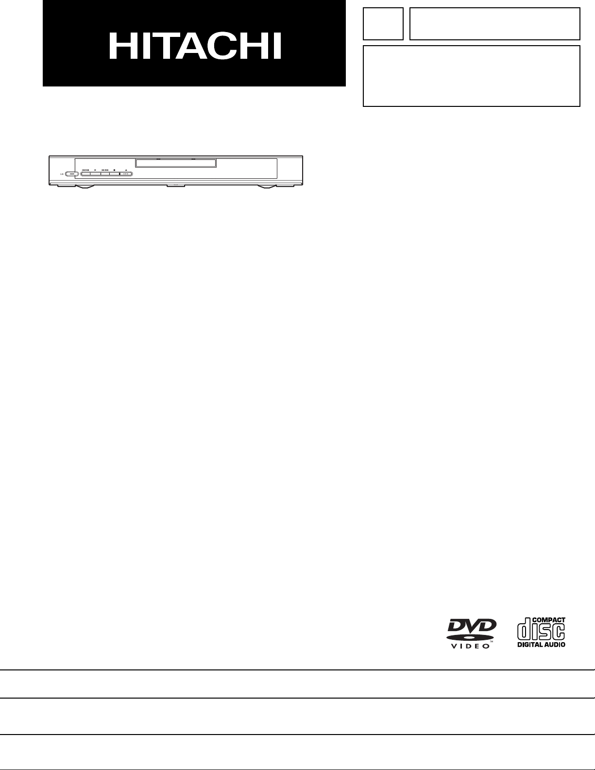
SERVICE MANUAL
TK No. 9303E
DV-P335E
DV-P335E(UK)
SPECIFICATIONS AND PARTS ARE SUBJECT TO CHANGE FOR IMPROVEMENT
DVD PLAYER
2003 Digital Media Division, TokaiApril
Page 2

CONTENTS
1 CAUTIONS FOR SAFETY IN PERFORMING
REPAIR . . . . . . . . . . . . . . . . . . . . . . . . . . . . . . . .1-1
1-1 LASER BEAM SAFETY PRECAUTIONS . . . . . . . . 1-1
1-2 IMPORTANT SAFETY PRECAUTIONS . . . . . . . . . 1-2
1-2-1 Product Safety Notice . . . . . . . . . . . . . . . . . . . . . 1-2
1-2-2 Precautions during Servicing. . . . . . . . . . . . . . . . 1-2
1-2-3 Safety Check after Servicing. . . . . . . . . . . . . . . . 1-3
1-3 STANDARD NOTES FOR SERVICING. . . . . . . . . . 1-4
1-3-1 Circuit Board Indications . . . . . . . . . . . . . . . . . . . 1-4
1-3-2 Instructions for Connectors . . . . . . . . . . . . . . . . . 1-4
1-3-3 How to Remove/Install Flat Pack-IC . . . . . . . . . . 1-4
1-3-4 Instructions for Handling Semi-conductors . . . . . 1-6
2 GENERAL INFORMATION. . . . . . . . . . . . . . . . .2-1
2-1 SPECIFICATIONS. . . . . . . . . . . . . . . . . . . . . . . . . . 2-1
2-2 COMPARISON OF MODELS . . . . . . . . . . . . . . . . . 2-2
2-3 OPERATING CONTROLS AND FUNCTIONS . . . . 2-4
3 MAINTENANCE AND INSPECTION. . . . . . . . . .3-1
3-1 TROUBLESHOOTING. . . . . . . . . . . . . . . . . . . . . . . 3-1
3-2 FIRMWARE RENEWAL MODE. . . . . . . . . . . . . . . . 3-7
3-2-1 How to Update the Firmware Version . . . . . . . . . 3-7
3-2-2 How to Verify the Firmware Version . . . . . . . . . . 3-7
SCHEMATIC AND BLOCK DIAGRAMS/CBA'S
1 SCHEMATIC DIAGRAMS/CBA’S AND TEST POINTS . 1
2 WIRING DIAGRAM. . . . . . . . . . . . . . . . . . . . . . . . . . . . . 3
3 SCHEMATIC DIAGRAMS. . . . . . . . . . . . . . . . . . . . . . . . 4
3-1 DVD Main 1/3 Schematic Diagram . . . . . . . . . . . . . . . 4
3-2 DVD Main 2/3 Schematic Diagram . . . . . . . . . . . . . . . 5
3-3 DVD Main 3/3 Schematic Diagram . . . . . . . . . . . . . . . 7
3-4 AV 1/3 Schematic Diagram . . . . . . . . . . . . . . . . . . . . . 8
3-5 AV 2/3 Schematic Diagram . . . . . . . . . . . . . . . . . . . . . 9
3-6 AV 3/3 & Function Schematic Diagram . . . . . . . . . . . 10
4 WAVEFORMS. . . . . . . . . . . . . . . . . . . . . . . . . . . . . . . . 11
5 CIRCUIT BOARD DIAGRAMS . . . . . . . . . . . . . . . . . . . 12
5-1 AV CBA Top View . . . . . . . . . . . . . . . . . . . . . . . . . . . 12
5-2 AV CBA Bottom View. . . . . . . . . . . . . . . . . . . . . . . . . 13
5-3 Function CBA Top/Bottom View . . . . . . . . . . . . . . . . 14
6 BLOCK DIAGRAMS . . . . . . . . . . . . . . . . . . . . . . . . . . . 15
6-1 System Control/Servo Block Diagram . . . . . . . . . . . . 15
6-2 Digital Signal Process Block Diagram . . . . . . . . . . . . 16
6-3 Video/Audio Block Diagram. . . . . . . . . . . . . . . . . . . . 17
6-4 Power Supply Block Diagram . . . . . . . . . . . . . . . . . . 18
7 SYSTEM CONTROL TIMING CHARTS . . . . . . . . . . . . 19
8 IC PIN FUNCTION DESCRIPTIONS . . . . . . . . . . . . . . 20
9 LEAD IDENTIFICATIONS. . . . . . . . . . . . . . . . . . . . . . . 21
4 DISASSEMBLY. . . . . . . . . . . . . . . . . . . . . . . . . .4-1
4-1 CABINET DISASSEMBLY INSTRUCTIONS. . . . . . 4-1
4-1-1 Disassembly Flowchart . . . . . . . . . . . . . . . . . . . . 4-1
4-1-2 Disassembly Method. . . . . . . . . . . . . . . . . . . . . . 4-1
5 EXPLODED VIEW AND PARTS LIST . . . . . . . .5-1
5-1 EXPLODED VIEW. . . . . . . . . . . . . . . . . . . . . . . . . . 5-1
5-2 REPLACEMENT PARTS LIST. . . . . . . . . . . . . . . . . 5-2
5-2-1 Mechanical Parts List . . . . . . . . . . . . . . . . . . . . . 5-2
5-2-2 Electrical Parts List . . . . . . . . . . . . . . . . . . . . . . . 5-3
Page 3
D
R
1
CAUTION FOR SAFETY IN PERFORMING REPAI
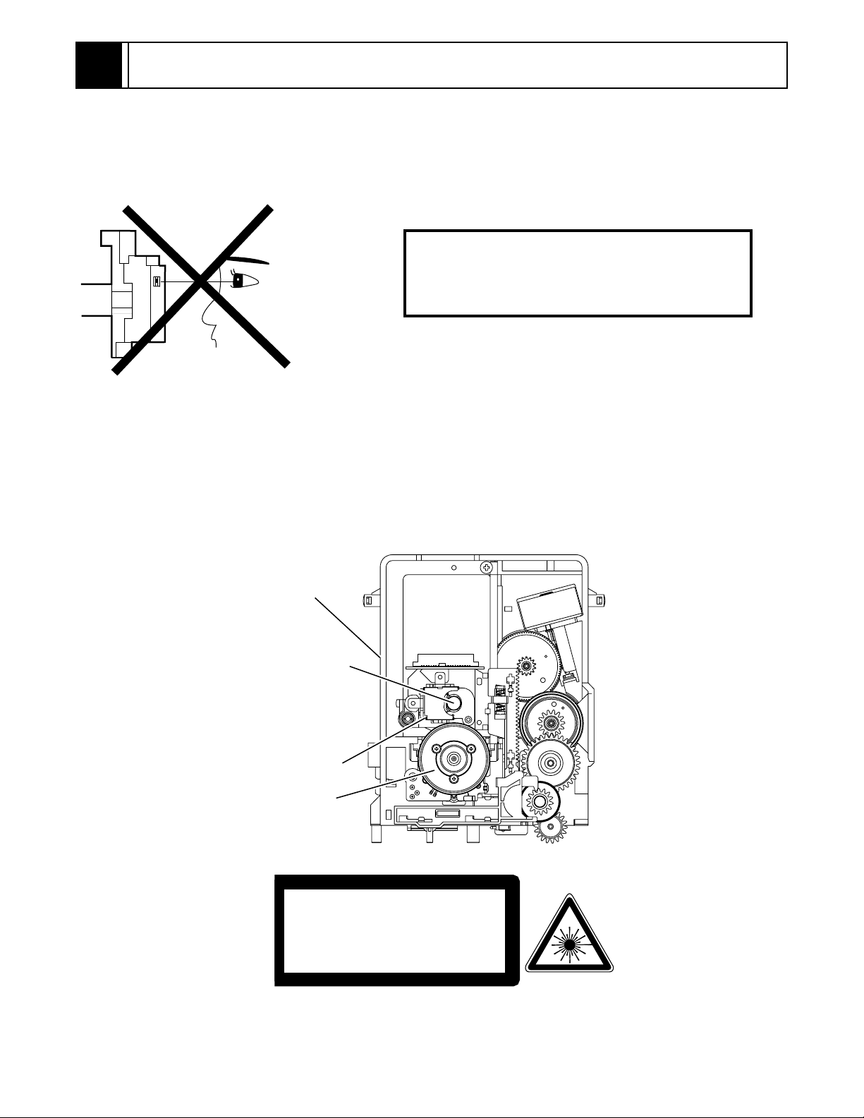
1-1 LASER BEAM SAFETY PRECAUTIONS
This DVD player uses a pickup that emits a laser beam.
Do not look directly at the laser beam coming
from the pickup or allow it to stri ke against your
skin.
The laser beam is emitted from the location shown in the figure. W hen checki ng the laser diode , be sure to keep
your eyes at leas t 30cm away f rom the pi ckup lens wh en the diod e is turned on. Do not l ook directl y at the las er
beam.
Caution: Use of controls and a djustments, or doing proce dures other than those s pecified herein, may r esult in
hazardous radiation exposure.
rive Mecha Assembly
Laser Beam Radiation
Laser Pickup
Turntable
CAUTION - VISIBLE LASER
RADIATION WHEN OPEN AND
INTERLOCK DEFEATED.
AVOID EXPOSURE TO BEAM.
Location: Inside Top of DVD mechanism.
1-1
Page 4

1-2 IMPORTANT SAFETY PRECAUTIONS
1-2-1 Product Safety Notice
Some electrical and mechanical parts have special
safety-related charac teristics which are often not evident from visual inspection, nor can the protection they
give necessarily be obtained by replacing them with
components rated for higher voltage, wattage, etc.
Parts that have special s afe ty c har ac te rist ic s ar e i den tified by a ! on schematics and in parts lists. Use of a
substitute replacement that does not have the same
safety characteristics as the recommended replacement part might create shock, fi re, and/or other hazards. The Product’s Safety is under review
continuously and new instructions are issued whenever appropriate. Prior to shipment from the factory,
our products are carefully inspected to confirm with
the recognized prod uct safety and electrical codes of
the countries in whic h th ey are to be sold. However, in
order to maintain such comp lianc e, it is equ ally impor tant to implement the following precautions when a set
is being serviced.
1-2-2 Precautions during Servicing
A. Parts identified by the ! symbol are critical for
safety. Replace only with part number specified.
B. In addition to safety, other parts and assemblies
are specified for conformance with regulations
applying to spur ious rad iation. T hese m ust also be
replaced only with specified re pla ce men ts.
Examples: RF converters, RF c ables, noise blocking capacitors, and noise blocking filters, etc.
C. Use specified internal wiring. Note especially:
1)Wires covered with PVC tubing
2)Double insulated wires
3)High voltage leads
D. Use specified insulating materials for hazardous
live parts. Note especially:
1)Insulation tape
2)PVC tubing
3)Spacers
4)Insulators for transistors
E. When replacing AC primary side components
(transformers, power cord, etc.), wrap ends of
wires securely about the terminals before soldering.
F. O bs erv e t hat the wi r es do n ot co ntact h eat pr od uc -
ing parts (heatsinks, oxide metal fil m re sisto rs, fus ible resistors, etc.).
G. Check that replaced wires do not contact sharp
edges or pointed parts.
H. When a power cord has been r eplaced, ch eck that
5 - 6 kg of force in any direction will not loosen it.
I. Also check areas surrounding repaired locations.
J. Be careful that foreign objects (screws, solder
droplets, etc.) do not remain inside the set.
K. Crimp type wire connector
The power tr ansformer uses crimp type connectors
which connect the power cord and the primary side
of the transformer. When replacing the transformer,
follow these steps carefully and precisely to prevent
shock hazards.
Replacement procedure
1)Remove the old connector by cutting the wires at a
point close to the connector.
Important: Do not re-use a connector. (Discard it.)
2)Strip about 15 mm of the insulation from the ends
of the wires. If the wires are stranded, twist the
strands to avoid frayed conductors.
3)Align the lengths of the wires to be connected.
Insert the wires fully into the connector.
4)Use a crimping tool to crimp the metal sleeve at its
center. Be sure to crimp fully to th e complete closure of the tool.
L. When connecting or disconnecting the internal
connectors, first, discon nect the AC plug from the
AC outlet.
1-2
Page 5
r
e)
Z
1-2-3 Safety Check after Ser vicing
Examine the area surrounding the repaired location for
damage or deterio ration. Observe that screws , parts,
and wires have been returned to their original positions. Afterwards, do the following tests and confirm
the specified values to verify compliance with safety
standards.
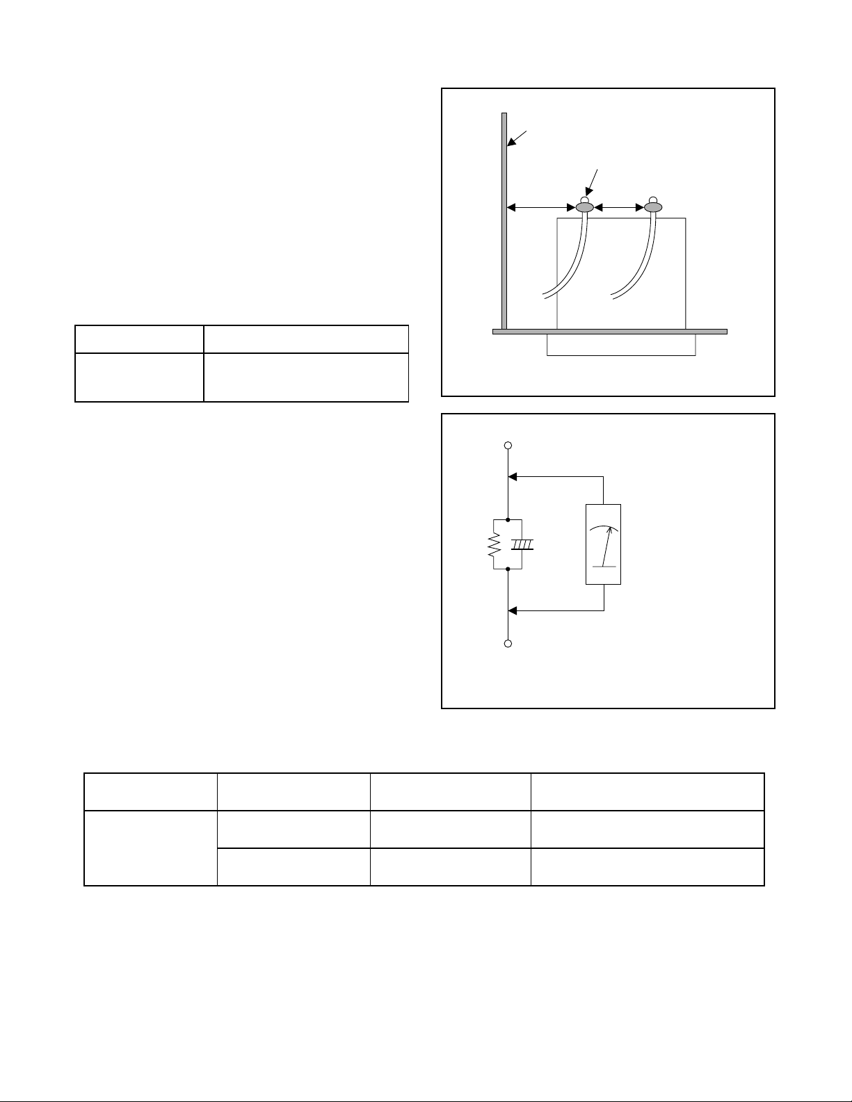
1. Clearance Distance
When replacing primary circuit components, confirm
specified cleara nce distanc e (d) and (d’) between sol dered terminals, and between terminals and surrounding metallic parts. (See Fig. 1-2-1)
T able 1-2-1 : Ratings for selected area
AC Line Voltage Clearance Distance (d) (d’)
Chassis or Secondary Conducto
Primary Circuit Terminals
dd'
230 V
Note: This table is unofficial and for reference only.
Be sure to confirm the precise values.
≥ 3 mm(d)
≥ 6 mm(d’)
2. Leakage Current Test
Confirm the specified (or lower) leakage current
between B (earth ground, power cord plug prongs)
and externally exposed accessible parts (RF terminals, antenna terminals, video and audio input and
output terminals, microphone jacks, earphone jacks,
etc.) is lower than or equal to the specified value in the
table below.
Measuring Method (Power ON) :
Insert load Z between B (earth ground, power cord
plug prongs) and exposed accessible parts. Use an
AC voltmeter to measure acr oss the ter minals of l oad
Z. See Fig. 1-2-2 and the following table.
Table 1-2-2: Leakage current ratings for selected areas
AC Line Voltage Load Z Leakage Current (i)
230 V
2kΩ RES.
Connected in parallel
50kΩ RES.
Connected in parallel
i≤0.7mA AC Peak
i≤2mA DC
i≤0.7mA AC Peak
i≤2mA DC
Exposed Accessible Part
One side of
B
Power Cord Plug Prongs
One side of power cord plug
Antenna terminals
A/V Input, Output
Fig. 1-2-1
AC Voltmeter
(High Impedanc
Fig. 1-2-2
prongs (B) to:
RF or
Note: This table is unofficial and for reference only. Be sure to confirm the precise values.
1-3
Page 6
1-3 STANDARD NOTES FOR SERVICING
O
P
P
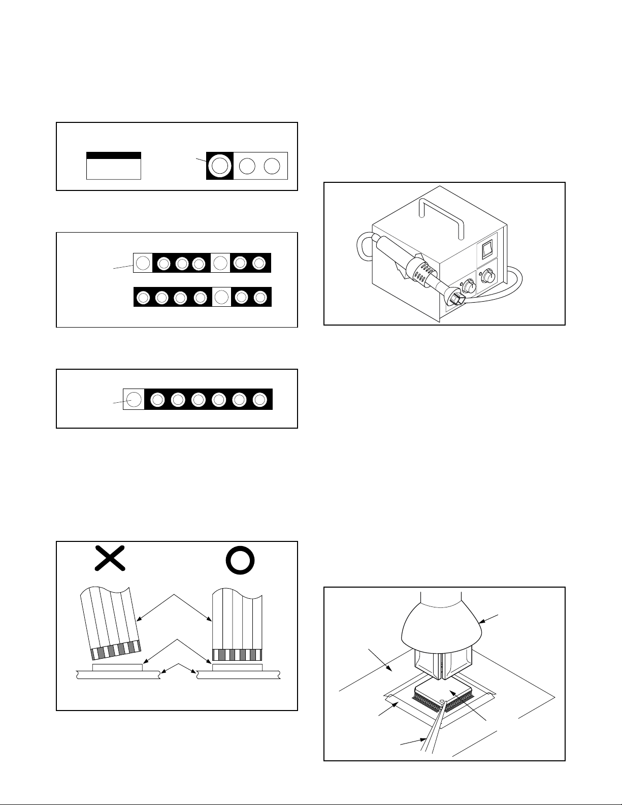
1-3-1 Circuit Board Indications
1. The output pin of the 3 pin Regulator ICs is indicated as shown.
Top View
Input
ut
2. For other ICs, pin 1 and every fifth pin are indicated
as shown.
In
in 1
3. The 1st pin of every male connector is indicated as
shown.
in 1
Bottom View
5
10
1-3-3 How to Remove / Install Flat
Pack-IC
1. Removal
With Hot-Air Flat Pack-IC Desoldering Machine:.
(1) Prepare the hot-air flat pack-IC desoldering
machine, then apply hot air to the Flat Pack-IC
(about 5 to 6 seconds). (Fig. 1-3-1)
Fig. 1-3-1
(2) Remove the flat pack-IC with tweezers while apply-
ing the hot air.
(3) Bottom of the flat pack-IC is fixe d with glue to the
CBA; when removing entire fl at pack-IC, fir st apply
soldering iron to center of the fla t pack-IC and hea t
up. Then remove (glue will be melted). (Fig. 1-3-6)
(4) Release the flat pack-IC from the CBA using twee-
zers. (Fig. 1-3-6)
1-3-2 Instructions for Connectors
1. When you connec t o r dis con nect the F FC (Flex ib le
Foil Connector) cable, be sure to first disconnect
the AC cord.
2. FFC (Flexible Foil Connector) cable should be
inserted parallel into the connector, not at an angle.
FFC Cable
Connector
CBA
* Be careful to avoid a short circuit.
Caution:
1. Do not supply hot air to the chip parts around the
flat pack-IC for over 6 seconds because damage to
the chip parts may occur. Put maskin g tape a r ound
the flat pack-IC to protect other parts from damage.
(Fig. 1-3-2)
2. The flat pack-IC on th e CB A i s affixed with glue, so
be careful not to break or damage the foil of each
pin or the solder lands under the IC when removing
it.
Hot-air
Flat Pack-IC
Desoldering
CBA
Masking
Tape
Tweezers
Machine
Flat Pack-IC
Fig. 1-3-2
1-4
Page 7
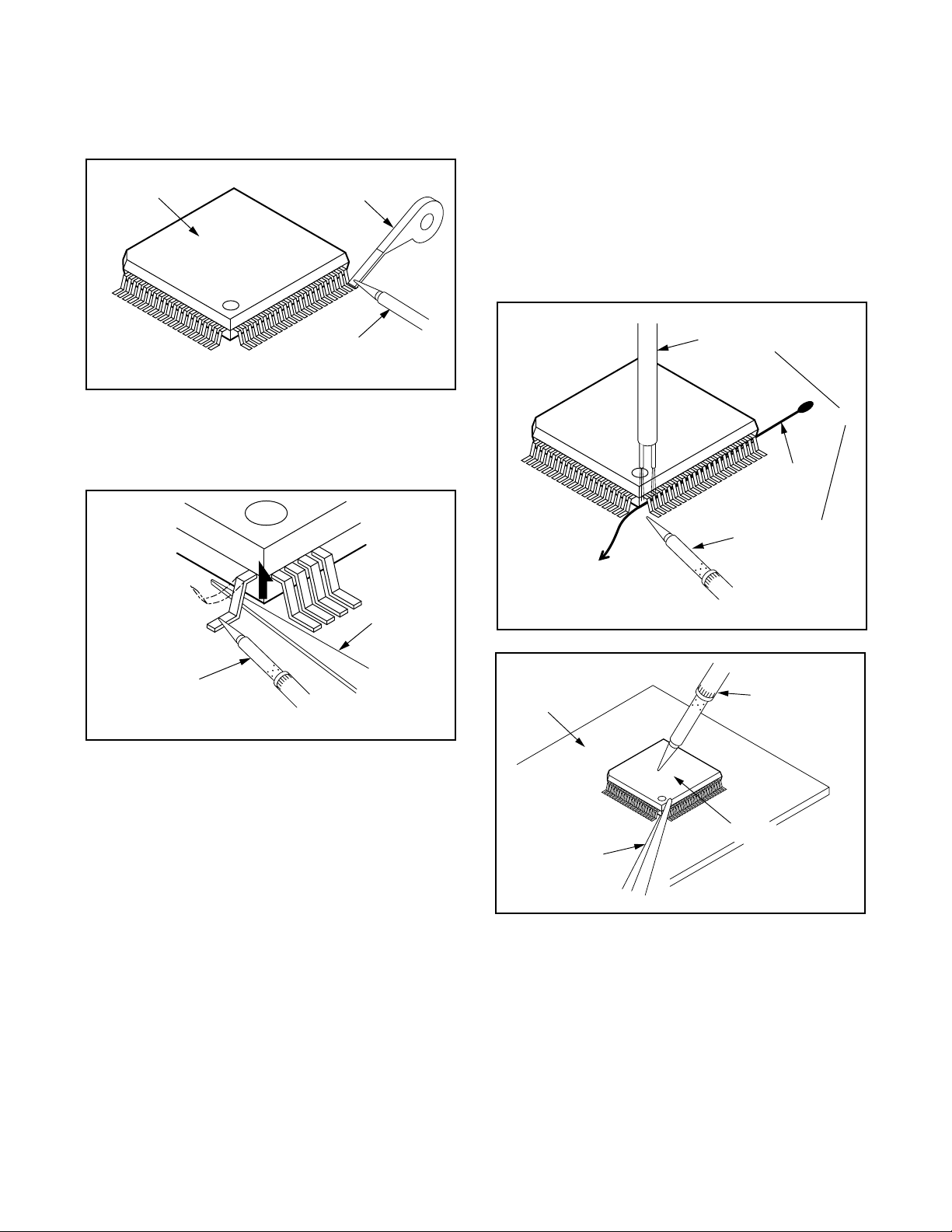
With Soldering Iron:
F
F
S
rp
or
n
(1)Using desoldering braid, remove the solder from all
pins of the flat pack-IC. Wh en you use solder flux
which is applied to all pins of the f lat pack-IC, you
can remove it easily. (Fig. 1-3-3)
lat Pack-IC
Desoldering Braid
(4) Bottom of the flat pack-IC is fixe d with glue to the
CBA; when removing entire fl at pack-IC, fir st apply
soldering iron to center of the fla t pack-IC and hea t
up. Then remove (glue will be melted). (Fig. 1-3-5)
(5) Release the flat pack-IC from the CBA using twee-
zers. (Fig. 1-3-6)
Note:
When using a sold ering iron, care must be taken
to ensure that the flat pack-IC is not being hel d by
glue. When the flat pack-IC is removed from the
CBA, handle it ge ntl y bec au se it may be damaged
if force is applied.
Soldering Iron
Hot Air Blower
Fig. 1-3-3
(2) Lift each lead of the flat pack-IC upward one by
one, using a sharp pin or wire to which sold er will
not adhere (iron wir e). When heati ng the pins, us e
a fine tip soldering iron or a hot air desoldering
machine. (Fig. 1-3-4)
Iron Wire
Soldering Iron
To Solid
Mounting Point
Sha
Fig. 1-3-5
Pin
ine Tip
oldering Iron
CBA
Fine Tip
Soldering Iro
Fig. 1-3-4
(3)B ottom of the flat pack-IC is fixed with glue to the
CBA; when removing enti re flat pack-IC, fi rst apply
soldering iron to c en ter o f th e f lat pack-I C an d h eat
up. Then remove (glue will be melted). (Fig. 1-3-6)
(4)Re lease the fla t pack-IC from the CBA us ing twee-
zers. (Fig. 1-3-6)
Tweezers
Flat Pack-IC
With Iron Wire:
(1)Using desoldering braid, remove the solder from all
Fig. 1-3-6
pins of the flat pack-IC. Wh en you use solder flux
which is applied to all pins of the f lat pack-IC, you
can remove it easily. (Fig. 1-3-3)
(2) Affix the wire to a workbench or solid mounting
point, as shown in Fig. 1-3-5.
(3) While heating the pins using a fine tip soldering
iron or hot air blower, pull up the wire as the solde r
melts so as to lift the IC leads from the CBA contact
pads as shown in Fig. 1-3-5
1-5
Page 8
2. Installation
P
i
d
(1) Using desoldering braid, remove the solder from
the foil of each pin of the flat pack-IC on the CBA
so you can install a replac ement flat pack-IC more
easily.
(2) The “I” mark on the flat pack-IC indicates pin 1.
(See Fig. 1-3-7.) Be sure this m ark matches the 1
on the PCB when position ing for installation. Then
presolder the four corners of the flat pack-IC. (S ee
Fig. 1-3-8.)
(3)Solder all pins of the flat pack-IC. Be sure that none
of the pins have solder bridges.
Example :
in 1 of the Flat Pack-IC
s indicated by a " " mark.
Fig. 1-3-7
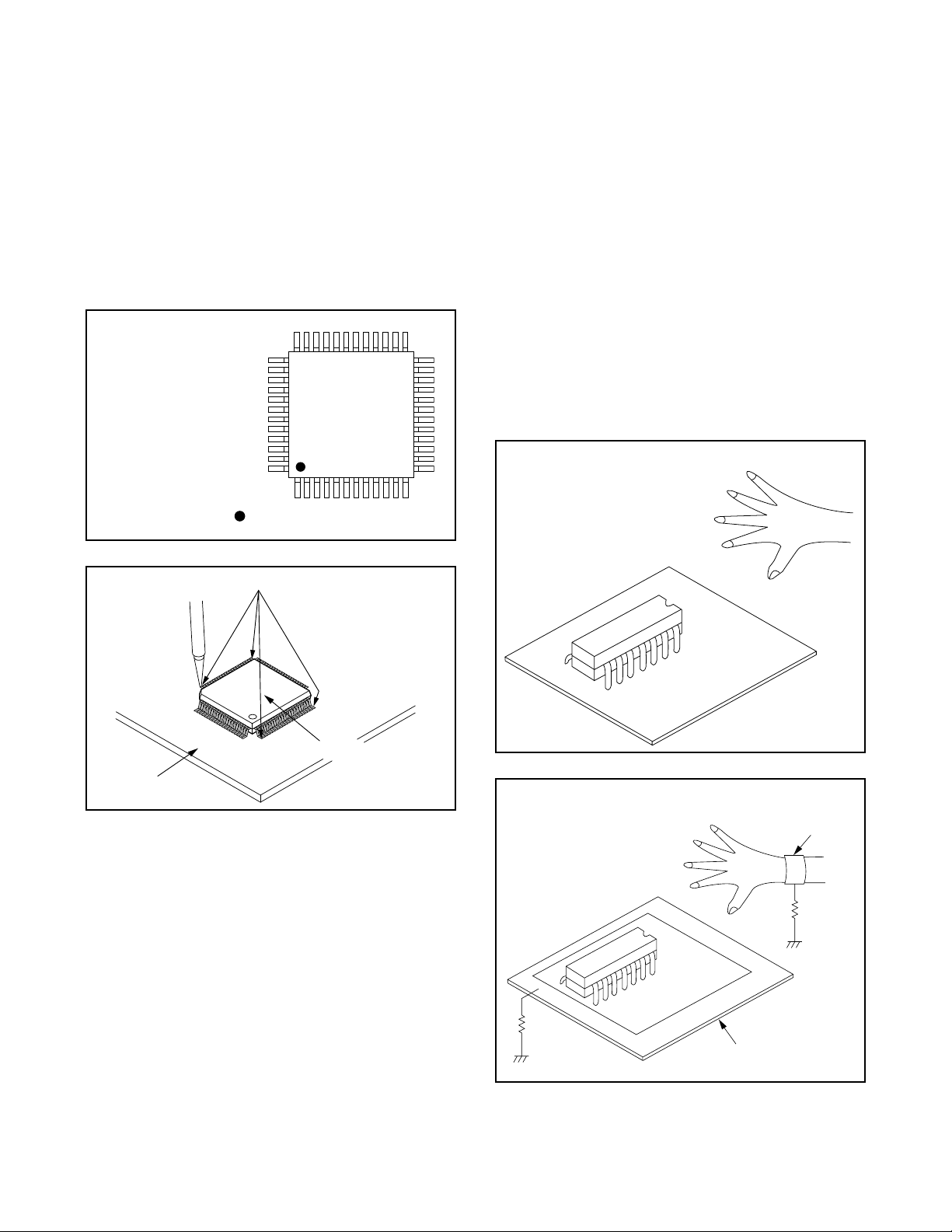
1-3-4 Instructions for Handling
Semi-conductors
Electrostatic breakdown of the semi-conductors may
occur due to a po tential difference ca used by electr ostatic charge during unpacking or repair work.
1. Ground for Human Body
Be sure to wear a gr oundin g band (1MΩ) that is properly grounded to re move any static electricity th at m ay
be charged on the body.
2. Ground for Workbench
(1) Be sure to place a conductive sheet or copper plate
with proper groundin g (1MΩ) on the workbench or
other surface, where the semi-conductors are to be
placed. Because the static electricity charge on
clothing will no t escape through the body grounding band, be careful to avoid contacting semi-conductors with your clothing.
< Incorrect >
CBA
Presolder
Flat Pack-IC
Fig. 1-3-8
CBA
< Correct >
Grounding Ban
1MΩ
CBA
1MΩ
Conductive Sheet or
Copper Plate
1-6
Page 9
GENERAL INFORMATION2
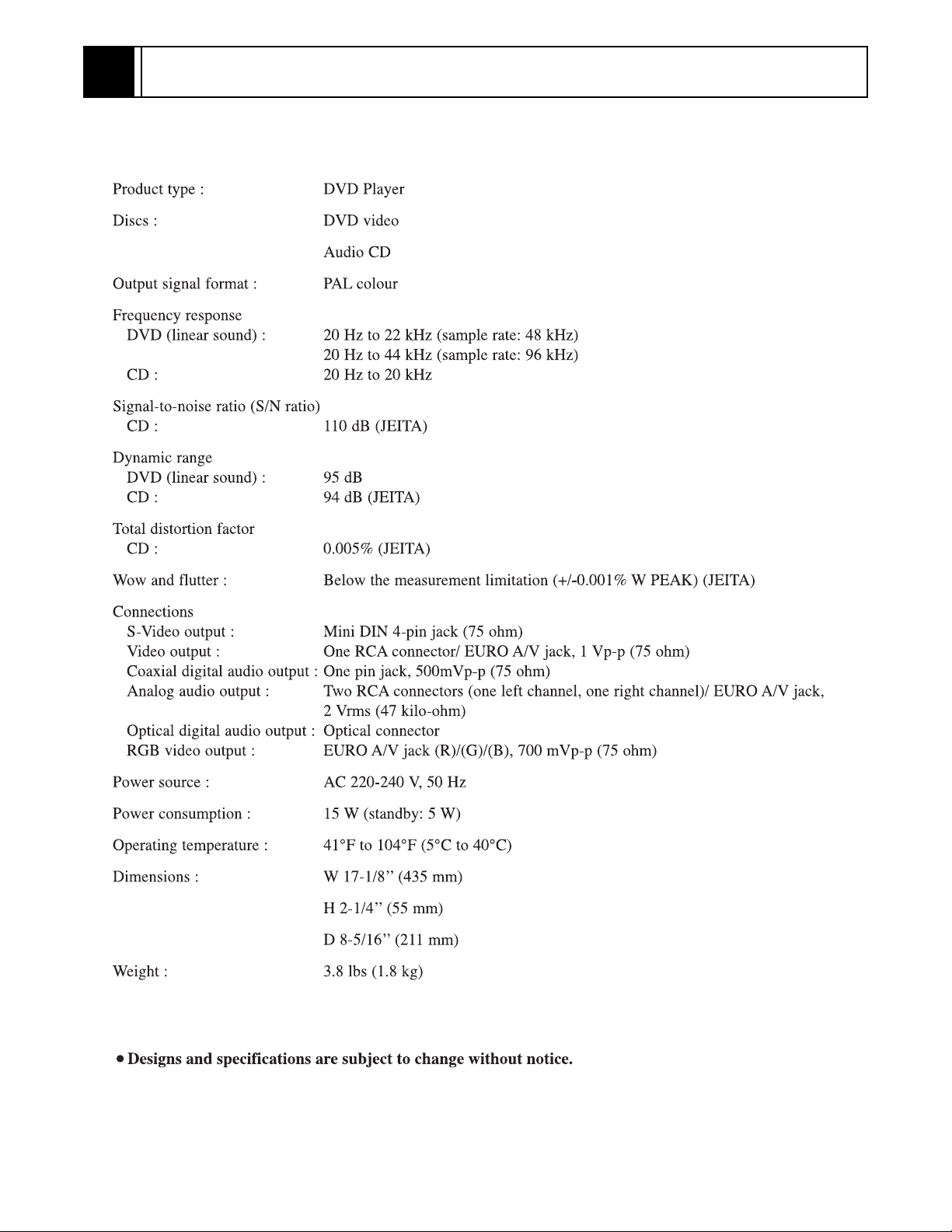
2-1 SPECIFICATIONS
2-1
Page 10
2-2 COMPARISON OF MODELS
A
E
G
L
V
O
A
O
T
Y
: The halftone parts are the differences from the previous model.
ITEM
Dimensional 435(W) x 55(H) x 211(D) mm 435(W) x 75(H) x 216(D) mm
Weight 1.8 kg 2.1 kg
Tray Panel Clear Silver
Color Front / Button Silver/Silver Black/Silver
Hot Stamp --- ---
PPEARANC
Ultra Vision Badge --- --Drive Speed 1x 1x
Laser 2 2
DVD/VCD/SVCD/CD-DA O / --- / --- / O O / --- / --- / O
CD-R/CD-RW/DVD-R (Video Format) O / O / O O / O / O
DVD-RAM (VR Format) --- --MP3 O O
ENERA
OSD languages
Jog Shuttle on Front --- Only switch shuttle
Headphone Jack / Volume --- / --- --- / --PAL Disc NTSC Out O --Video Out Mode NTSC/PAL/PAL60 --- / O / O --- / O / O
S-Video / Component / Composite O / O / O O / O / O
Video D/A Converter 10bit 10bit
IDE
Black Level Select --- O
Picture Control --- --Progressive Out --- --Audio D/A Converter 192kHz / 24bit 192kHz / 24bit
Digital Audio Out Optical / Coaxial O / O O / O
Dolby Digital 5.1 ch Decode --- --DTS Digital Out O O
Virtual Surround O O
UDI
Dynamic Range Compression (Dolby
Digital)
DVD Audio --- --Power on sound --- ---
Search Speed
Slow Speed 1/16, 1/8, 1/2 (FORWARD/REWIND) 1/16, 1/8, 1/2 (FORWARD only)
IP Search (Smooth 2x Play) O O
2x Play with Audio --- ---
RICK PLA
Step Forward / Reverse O / --- O / --Still Picture Select (Frame/Field) Auto Only Auto Only
DV-P335E/P335E(UK) DV-P325E/P325E(UK)
7 (English, French, Spanish
Italian, German, Swedish, Dutch)
2 to 100 (FORWARD/REWIND)
(DVD: 2, 8, 50, 100/CD: 16)
7 (English, French, Spanish
Italian, German, Swedish, Dutch)
OO
2 to 60 (FORWARD/REWIND)
(DVD: 2, 8, 30, 60/CD: 16)
2-2
Page 11
ITEM
F
S
C
R
Disc Navigation O --DVD Zoom x2 / x4 / x16 O / O / --- O / O / --Program and Random Play of DVD --- --A-B Repeat O O
Repeat O O
Resume Play
EATURE
Front Panel Display Dimmer O O
Screen Saver O O
Auto Power Off O O
Jog Shuttle on Remote --- ---
REMOTE
TV Control --- ---
ONTROLLE
DV-P335E/P335E(UK) DV-P325E/P325E(UK)
O (Resume is not effected after
power off)
O
2-3
Page 12
e
RGBAV TV
ANALOG
AUDIO OUT
DIGTAL
AUDIO OUT
COAXIALOPTICAL
S-VIDEO
OUT
VIDEO
OUT
LR
12345
B
C
A
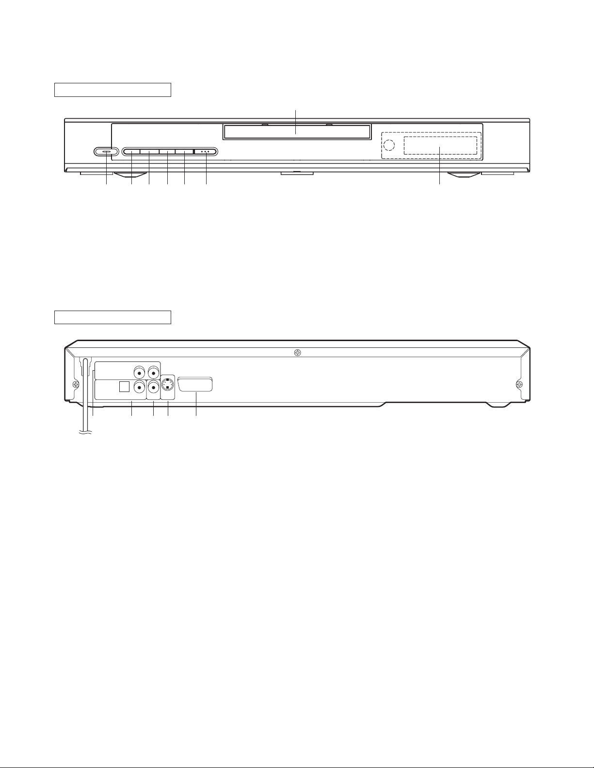
2-3 OPERATING CONTROLS AND FUNCTIONS
FRONT PANEL
7
y/I
H/ED/GABC
1 6
1. y/I (POWER/STANDBY)
to switch the player to ON or OFF
(As to the indication of the Operate switch, “I” indicates
ON and “y” indicates electrical power STANDBY)
2. SKIP/FR
goes to previous chapter or track during playback;
press and hold for 1.5 seconds for a reverse search
B
3.
(PLAY)
to start or resume disc playback
REAR PANEL
82 3 4 5
4. FF/SKIP
goes to next chapter or track during playback; press
and hold for 1.5 seconds for a forward search
C
(STOP)
5.
to stop playback
A
6.
(OPEN/CLOSE)
to open/close the disc tray
7. Disc tray
8. Display
1. ANALOG AUDIO OUT JACKS
Connect to the Audio input jacks of A/V-compatible TV
or wide screen TV, Stereo system.
2. DIGITAL AUDIO OUT JACKS:
Use either an optical or coaxial digital cable to connect
to a compatible Dolby Digital receiver. Use to connect to
a Dolby Digital decoder or DTS decoder.
3. VIDEO OUT JACK
Use a video cable to connect one of the jack to Video
input on your A/V-compatible TV or wide screen TV,
Stereo system.
2-4
4. S-VIDEO OUT JACK
Use the S-Video cable to connect this jack to the SVideo jack on your A/V-compatible TV or wide screen
TV for a higher quality picture.
5. EURO A/V (SCART) JACK
Use the Euro audio/video cable to connect this jack to
the 21 pin scart jack on your A/V-compatible TV or wid
screen TV for a best quality picture.
Page 13
B
o
H
s
C
h
F
g
B
G
d
.
A
Title/Chapter/Track/Time.
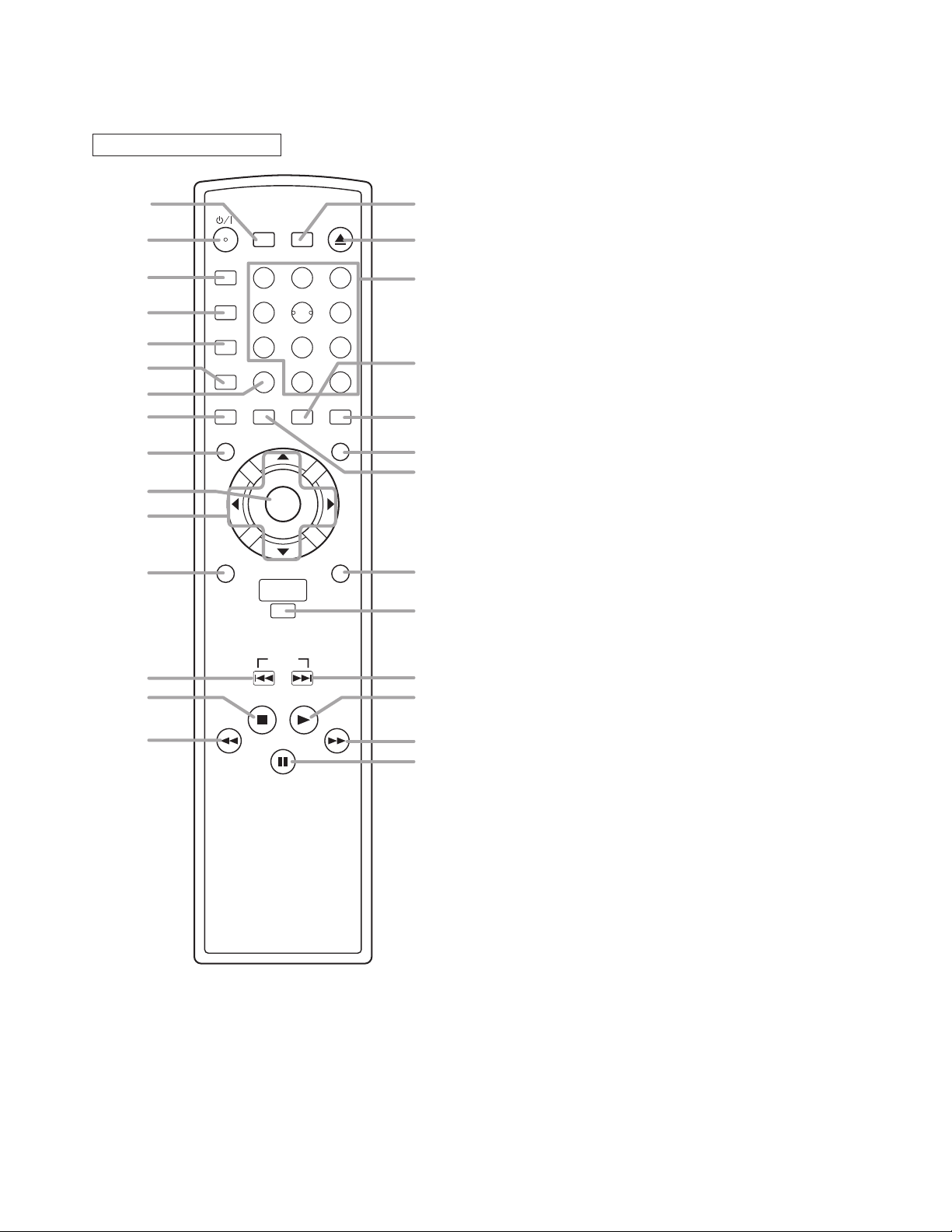
REMOTE CONTROL
1
SURROUND
2
A-B REPEAT
ZOOM
1
4
7
CLEAR
SUBTITLE
3
REPEAT
4
5
MODE
6
7
ANGLE
8
MENU
9
10
ENTER
11
RETURN
12
NAVIGATION
13
14
15
SEARCH OPEN/
MODE
2
56
8
0
AUDIO
DISC
SKIP
CLOSE
3
9
+10
DISPLAY
TOP MENU
SETUP
28
27
26
25
24
23
22
21
20
19
18
17
16
1. SURROUND
Press to activate the virtual sound.
2. y/I (POWER/STANDBY)
to switch the player to ON or OFF
(As to the indication of the Operate switch, “I” indicates
ON and “y” indicates electrical power STANDBY)
3. A-B REPEAT
Repeats playback of a selected section.
4. REPEAT
Repeats playback of the current disc, title, chapter or
track.
5. MODE
to set up programmed or random playback (Audio CD)
to set the virtual surround during DVD playback
6. ZOOM
enlarge DVD video image
7. CLEAR
8. ANGLE
select DVD camera angle
9. MENU
to display the menu of the DVD disc
10. ENTER
acknowledge menu selection
11. Arrow Buttons (
Move the cursor and determines its position.
12. RETURN
to return previous or remove setup menu
13. SKIP
14.
15.
16.
17.
18.
19. SKIP
20. DISC NAVIGATION
21. SETUP
22. SUBTITLE
23. TOP MENU
24. DISPLAY
25. AUDIO
26. Numerical Buttons
27.
28. SEARCH MODE
H
goes to previous chapter or track during playback; pres
and hold for 1.5 seconds for a reverse search
C
to stop playback
h
to view DVD picture in fast reverse motion
F
Press to pause Disc playback. Press repeatedly to
advance the DVD picture step by step (or one frame at
a time).
g
to view DVD picture in fast forward motion
B
to start or resume disc playback
goes to next chapter or track during playback; press an
hold for 1.5 seconds for a forward search
Press to display the first scenes of each chapter of the
title being played.
Press to enter the setup mode.
Press to select the desired subtitle language.
Press to call up the title menu.
Press to access or remove the display screen during
DVD or Audio CD playback.
Press to select a desired audio language or sound
mode.
Press to directly select a Track (Audio CD) for playback
A
to open/close the disc tray
Press to access or remove the Search display, which
allows you to go directly to a specific
(STOP)
(PAUSE/STEP
(PLAY)
G
(OPEN/CLOSE)
ss B
ppo
)
2-5
Page 14
MAINTENANCE AND INSPECTION3
,
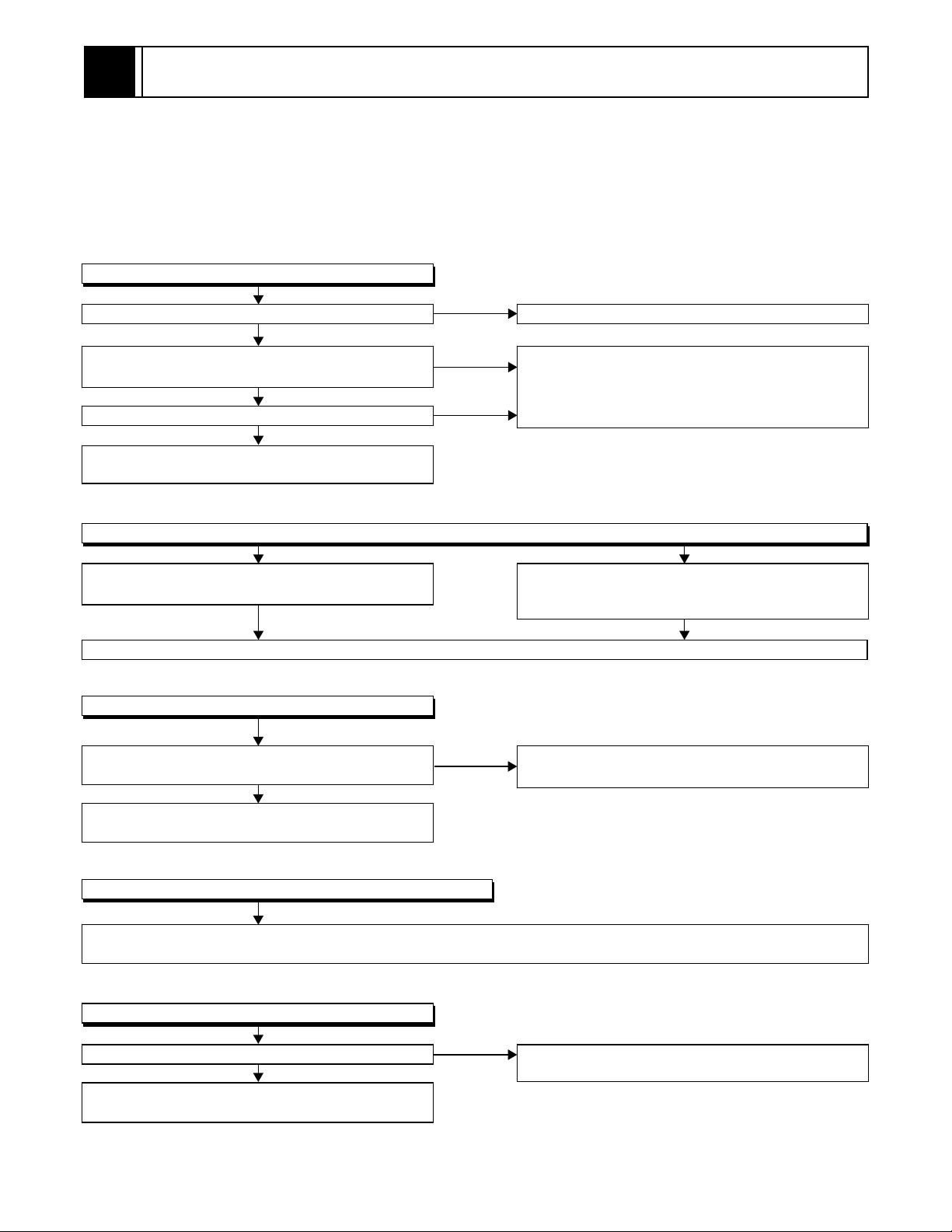
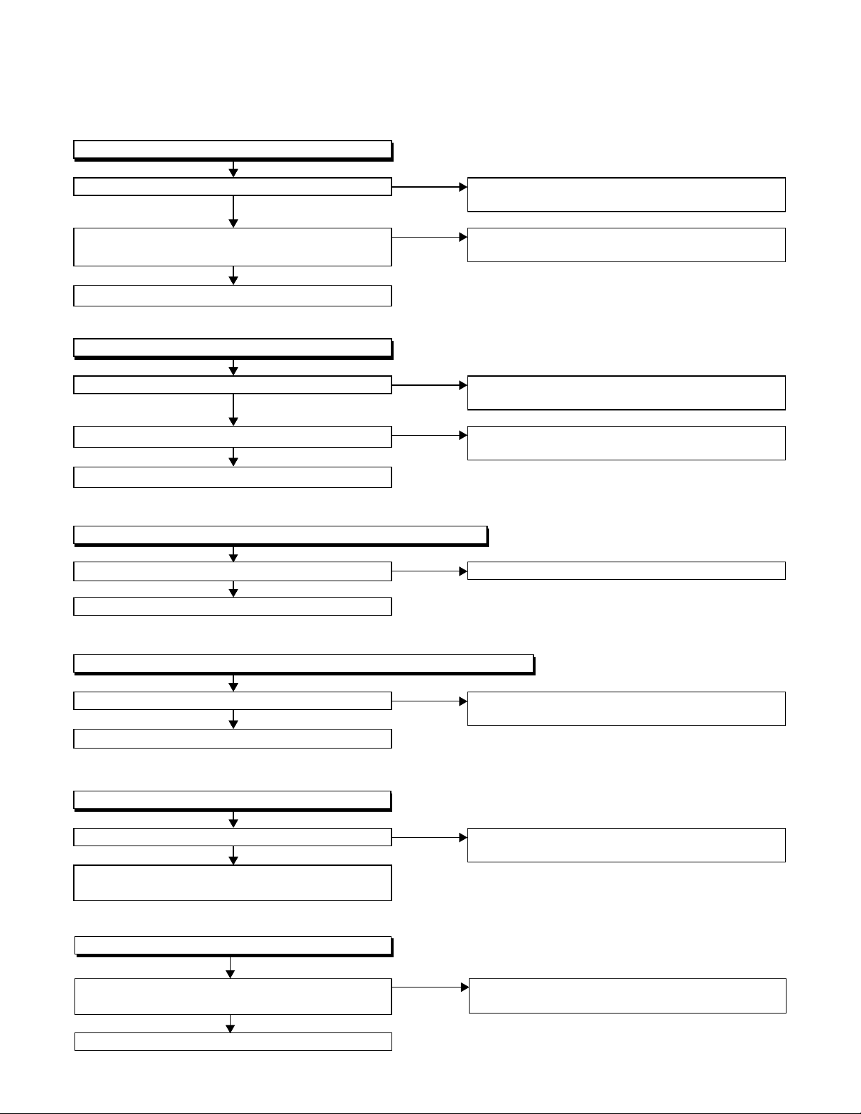
3-1 TROUBLESHOOTING
Troubleshooting is how to service for the specifying malfunction or poor parts.
Detect malfunction or poor parts and service as the following charts.
FLOW CHART NO.1
The power cannot be turned on.
Is the fuse normal?
Yes
Is normal state restored when once unplugged
power cord is plugged again after several seconds?
Yes
Is the EV+3.3V line voltage normal?
Yes
Check each rectifying circuit of the secondary circuit
and
service it if defective.
FLOW CHART NO.2
The fuse blows out.
Check the presence that the primary component
is leaking or shorted and service it if defective.
After servicing, replace the fuse.
FLOW CHART NO.3
When the output voltage fluctuates.
Does the photo coupler circuit on the secondary
side operate normally?
Yes
Check IC1001, D1012, D1024 and their periphery,
and service it if defective.
No
No
No
No
See FLOW CHART No.2 <The fuse blows out.>
Check if there is any leak or short-circuiting on the
primary circuit component,
defective. (Q1001, Q1003, T1001, D1001, D1002,
D1004, D1005, D1011, C1003, C1005)
Check the presence that the rectifying diode or
circuit is shorted in each rectifying circuit of
secondary side, and service it if defective.
Check IC1001, IC1006, D1015, D1048 and their
periphery, and service it if defective.
and
service it if
FLOW CHART NO.4
When buzz sound can be heard in the vicinity of power circuit.
Check if there is any short-circuit on the rectifying diode and the circuit in each rectifying circuit of the secondary side
and service it if defective.
FLOW CHART NO.5
-FL is not outputted.
Is -24V voltage supplied to the anode of D1003?
Check if there is any leak or short-circuit
on the loaded circuit, and service it if defective.
(D1003, D1006, D1008, D1016, D1030, IC1002, Q1002, Q1004, Q1011, Q1050)
Yes
No
Check D1003 and periphery circuit, and service it
if defective.
3-1
Page 15
.
FLOW CHART NO.6
P-ON+12V is not outputted.
Is 12V voltage supplied to the emitter of Q1002?
Yes
Is the voltage of base on Q1002 lower than the
voltage of emitter on Q1002 when turning the power on?
Yes
Replace Q1002.
FLOW CHART NO.7
EV+9V is not outputted.
Is 9V voltage supplied to the collector of Q1050?
Yes
Is the "H" pulse inputted into the base of Q1050?
Yes
Replace Q1050.
FLOW CHART NO.8
P-ON+5V is not outputted. (EV+9V is outputted normally.)
Is the "H" pulse inputted into the base of Q1004?
Yes
Replace Q1004.
No
No
No
No
No
Check D1030, D1048, L1009, C1035, C1048 and
the periphery circuit, and service it if defective.
Check Q1016 and PWRCON line and service it if
defective.
Check D1030, D1048, L1009, C1035, C1048, R1097
and the periphery circuit, and service it if defective.
Check D1072, C1070, R1098 and service it if
defective.
Check R1068 and D1046, and service it if defective
FLOW CHART NO.9
P-ON+3.3V (EV+3.3V) is not outputted. (P-ON+12V is outputted normally.)
Is 3.3V voltage supplied to the collector of Q1011?
Yes
Replace Q1011 and R1067.
FLOW CHART NO.10
EV+5V is not outputted.
Is EV+9V outputted normally?
Yes
Check D1047 and the periphery circuit, and
service it if defective.
FLOW CHART NO.11
EV+1.5V is not outputted.
Is approximately 2.5V voltage supplied to Pin(1)
of IC1002?
Yes
Replace IC1002.
No
No
No
Check D1008, D1015, C1007, C1038 and the
periphery circuit, and service it if defective.
Refer to "FLOW CHART NO.6"
<EV+9V is not outputted.>
Check D1006,C1014,C1050, and their periphery,
and service it if detective.
3-2
Page 16

.
FLOW CHART NO.12
.
The fluorescent display tube does not light up.
Is 3.3V voltage supplied to Pin(6) and
Pin(24) of IC2001?
Yes
Is the voltage of approximately -24V to -28V
supplied to Pin(15) of IC2001?
Yes
Is there 500kHz oscillation at Pin(26) of IC2001?
Yes
Are the filament voltage supplied between
Pins(1, 2) and Pins(34, 35) of the fluorescent
display tube? And the negative voltage applied
between these pins and GND?
Yes
Replace the fluorescent display tube.
FLOW CHART NO.13
The key operation is not functioning.
Are the contact point and the installation state of the
key switches (SW2002, 2003, 2005-2008) normal?
Yes
When pressing each switches (SW2002-2003,
2005-2008), do the voltage of each pin
of IC2001 (shown below) switch to 75mV from
6mV?
SW2002, 2006, 2008 : IC2001 3PIN
SW2003, 2005, 2007 : IC2001 4PIN
Yes
Replace IC2001.
No
No
No
No
No
No
Check the EV+3.3V line and service it if detective.
Check the -FL (-28V) line and service it if detective
Check R2015, IC2001 and their periphery, and
service it if detective.
Check D1016, D1017, R1079, C1018, and their
periphery, and service it if detective.
Re-install the switches (SW2002, 2003,
2005-2008) correctly or replace the poor switch.
Check the switches (SW2002, 2003, 2005-2008)
and their periphery, and service it if detective.
FLOW CHART NO.14
No operation is possible from the remote control unit.
Operation is possible from the DVD, but no
operation is possible from the remote control unit.
Yes
Is 5V voltage supplied to the Pin(3) terminal of
the infrared remote control receiver (RM2001)?
Yes
Is the "L" pulse sent out Pin(1) terminal of receiver
(RM2001) when the infrared remote control is activated?
Yes
Is the "L" pulse signal supplied to the Pin(22) of
CN1001?
Yes
Replace DVD Main CBA.
No
No
No
Check EV+5V line and service it if detective.
Replace the infrared remote control receiver (RM2001)
Or replace the remote control unit.
Check the line between Pin(1) of the infrared
remote control receiver (RM2001) and Pin(22) of
CN1001, and service it if detective.
3-3
Page 17

FLOW CHART NO.15
The disc tray cannot be opened and closed. (It can be done using the remote control unit.)
Does the voltage of Pin(4) on IC2001 become 75mV
when pressing "OPEN/CLOSE" button on the unit?
Yes
Refer to "FLOW CHART NO.16" <The disc tray
cannot be opened and closed.>
FLOW CHART NO.16
The disc tray cannot be opened and closed.
Replace the DVD Main CBA.
No improvement can be found.
Yes
Replace the DVD Mecha.
FLOW CHART NO.17
[No Disc] indicated. (When the focus error occurs.)
Replace the DVD Main CBA.
No improvement can be found.
Yes
Replace the DVD Mecha.
No
No
No
Replace the "OPEN/CLOSE" button (SW2005).
Original DVD Main CBA is poor.
Original DVD Main CBA is poor.
FLOW CHART NO.18
[No Disc] indicated. (When the focus servo is not functioning.)
Replace the DVD Main CBA.
No improvement can be found.
Yes
Replace the DVD Mecha.
FLOW CHART NO.19
[No Disc] indicated. (When the laser beam does not light up.)
Replace the DVD Main CBA.
No improvement can be found.
Yes
Replace the DVD Mecha.
No
No
Original DVD Main CBA is poor.
Original DVD Main CBA is poor.
3-4
Page 18

FLOW CHART NO.20
Both functions of picture and sound do not operate normally.
Replace the DVD Main CBA.
No improvement can be found.
Yes
Replace the DVD Mecha.
FLOW CHART NO.21
Picture does not appear normally.
Set the disc on the disc tray, and playback.
Are the video signals outputted to each pin of
CN1601 on the AV CBA?
CN1601 1PIN S-Y
CN1601 9PIN S-C
CN1601 7PIN G
CN1601 5PIN B
CN1601 3PIN R
Yes
Are the video signals shown above inputted into
each pin of IC1401?
IC1402 6PIN S-Y
IC1402 2PIN S-C
IC1402 16PIN G
IC1402 12PIN B
IC1402 14PIN R
Yes
Are the video signals outputted to each pin
of IC1401?
No
No
No
Original DVD Main CBA is poor.
Replace the DVD Main CBA or DVD Mecha.
Check the line between each pin of CN1601 and
each pin of IC1401 on the AV CBA, and service it
if detective.
CN1601 1PIN → IC1402 6PIN S-Y
CN1601 9PIN → IC1402 2PIN S-C
CN1601 7PIN → IC1402 16PIN G
CN1601 5PIN → IC1402 12PIN B
CN1601 3PIN → IC1402 14PIN R
IC1402 31PIN CVBS
IC1402 28PIN S-Y
IC1402 33PIN S-C
IC1402 19PIN G
IC1402 25PIN B
IC1402 22PIN R
Yes
Are the video signals outputted to the specific
output terminal?
Are the luminance signals outputted to the
S-OUT terminal (JK1401)?
Are the chroma signals outputted to the
S-OUT terminal (JK1401)?
Are the component video signals outputted to the
VIDEO OUT terminal (JK1404)?
Are the composite video signals outputted to
the VIDEO OUT terminal (JK1404)?
No
No
No
No
No
Is 5V voltage applied to the pin(1, 24) of
IC1401?
Yes No
Replace IC1401. Check P-ON+5V line and
service it if detective.
Check the periphery of JK1401 from
Pin (28) of IC1401 and service it if detective.
Check the periphery of JK1401 from
Pin (33) of IC1401 and service it if detective.
Check the periphery of JK1404 from Pins (19, 22,
25) of IC1401 and service it if detective.
Check
the periphery of
IC1401
and service it if detective.
JK1404 from Pin(31) of
3-5
Page 19

FLOW CHART NO.22
Audio is not outputted.
Set the disc on the disc tray, and playback.
Are the analog audio signals outputted to each pin
of CN1601 on AV CBA?
CN1601 13PIN AUDIO-L
CN1601 15PIN AUDIO-R
Yes
Are the analog audio signals inputted to each pin
of IC1201?
IC1201 2PIN AUDIO-L
IC1201 6PIN AUDIO-R
Yes
Is the "H" level mute signal outputted to CN1601
on AV CBA ?
CN1601 12PIN A-MUTE
CN1601 16PIN A-R-MUTE
CN1601 14PIN A-L-MUTE
Yes
Are the analog audio signals inputted to each pin
of IC1201?
IC1201 1PIN AUDIO-L
IC1201 7PIN AUDIO-R
Yes
Are the audio signals outputted to the specific
output terminal?
Are the audio signals outputted to the audio
terminal (JK1402)?
No
No
No
No
No
Replace the DVD Main CBA or DVD Mecha.
Check each line between each pin of CN1601
and each pin of IC1201 on AV CBA, and service it
if detective.
CN1601 13PIN → IC1201 2PIN AUDIO-L
CN1601 15PIN → IC1201 6PIN AUDIO-R
Replace the DVD Main CBA or DVD Mecha.
Replace IC1201.
Check the periphery between Pins(1,7) of IC1201
and JK1402, and service it if detective.
3-6
Page 20

3-2 FIRMWARE RENEWAL MODE
F
e
F
e)
F
n
F
e)
3-2-1 How to Update the Firmware Ver-
sion
1. Turn the power on and remove the disc on the tray.
2. To put the DVD player into v ersion up mo de, pr ess
[9], [8], [7], [6], and [SEARCH MODE] buttons on
the remote control un it in that order. The tray will
open automatically.
Fig. 3-2-1 appears on the screen and Fig. 3-2-2
appears on the VFD.
The DVD player can also enter the version up
mode with the tray open. In this case, Fig. 3-2-1 will
be shown on the screen while the tray is open.
5. After programming is fi nish ed, the tray opens au tomatically. Fig. 3-2-5 appears on the scree n an d the
checksum in (*3) of Fig. 3-2-5 appears on the VFD.
(Fig. 3-2-6)
At this time, no buttons are available.
AppearanceNo. State
Reading... Sending files into the memory
1
Erasing... Erasing previous version data
2
Programming...
3 Writing new version data
F/W Version Up Mode
Please insert a DISC
for F/W Version Up.
EXIT: POWER
Fig. 3-2-1 Version Up Mode Screen
ig. 3-2-2 VFD in Version Up Mod
3. Load the disc for version up.
4. The DVD player ente rs the F/W version up mode
automatically. Fig. 3-2-3 appears on the screen and
Fig. 3-2-4 appears on the VFD.
F/W Version Up Mode
VERSION : ********
Reading...(*2)
EXIT: POWER
Fig. 3-2-3 Programming Mode Screen
F/W Version Up Mode
VERSION : ********
Completed
SUM : 7abc (*3)
ig. 3-2-5 Completed Program Mode Scree
ig. 3-2-6 VFD upon Finishing the Programming Mode (Exampl
6. Unplug the AC cord from the AC outlet. Then plug it
again.
7. To finish this mode, press [POWER] button.
3-2-2 How to Verify the Firmware Ver-
sion
1. After making sure that no disc is in unit, turn the
power on.
2. Press [1], [2], [3], [4], and [DISPLAY] buttons on the
remote control un it in that order. The B/E version
appears on the VFD , and th e F /E an d B/E ve rsio ns
appear on TV screen.
3. Turn the power off to reset the unit.
Note:
If the firmware has been changed, etc., we will use
Service News, etc. to report on how to obtain new
firmware data and create an upgraded disc.
ig. 3-2-4 VFD in Programming Mode (Exampl
The appearance shown in (*2) of Fig. 3-2-3 is
described as follows:
3-7
Page 21

DISASSEMBLY 4
4-1 CABINET DISASSEMBLY INSTRUCTIONS
4-1-1 Disassembly Flowchart
This flowchart indicates the disassem bly steps to gain
access to item(s) to be serviced. When reassembling,
follow the steps in reverse order. Bend, route, and
dress the cables as they were originally.
[1] Top Cover
[2] Front Assembly
[3] DVD Mecha
[5] DVD Main CBA[4] AV CBA
[7] Main CBA Holder[6] Function CBA
[8] Rear Panel
4-1-2 Disassembly Method
ID/
LOC.
No.
[1] Top Cover 4 -1 -1 5(S-1) -
[2]
[3]
[4] AV CBA 4-1-5
[5]
[6]
[7]
[8]
(1)
↓
PART
Front
Assembly
DVD
Mecha
DVD Main
CBA
Function
CBA
Main CBA
Holder
Rear
Panel
↓
(2)
Fig.
No.
4-1-2
4-1-3,
4-1-4
4-1-5 2(S-5) -
4-1-5 Desolder -
4-1-6 (S-6) -
4-1-6 (S-7) -
↓
(3)
REMOVAL
REMOVE/*UNHOOK/
UNLOCK/RELEASE/
UNPLUG/DESOLDER
*2(L-1), Tray Panel,
*2(L-2), *5(L-3),
*3(L-4)
*CN301, 3(S-2),
*CN201
5(S-3), 3(S-4),
*CN1001, *CN1601
↓
(4)
Note
1-1
1-2
1-3
1-4
1-5
1-6
2
2-1
2-2
2-3
3
-
↓
(5)
(1): Identification (location) No. of parts in the figures
(2):Name of the part
(3):Figure Number for reference
(4): Identification of parts to be removed, unhooked,
unlocked, released, unplugged, unclamped, or
desoldered.
P=Spring, L=Locking Tab, S=Scr ew,
CN=Connector
*=Unhook, Unlock, Release, Unplug, or Desolder
e.g. 2(S-2) = two Screws (S-2),
2(L-2) = two Locking Tabs (L-2)
(5):Refer to “Reference Notes.”
Reference Notes
CAUTION 1: Locking Tabs (L-1), (L-2), (L-3) and (L-4)
are fragile. Be careful not to break them.
1-1. Connect the wall plug to an AC outlet and pres s
the OPEN/CLOSE button to open the Tray.
1-2. Remove the Tray Panel by releasing two Locking
Tabs (L-1).
1-3. Press the OPEN/CLOSE button again to close
the Tray.
1-4. Press the POWER button to turn the power off.
and unplug an AC cord.
1-5. Release two Locking Tabs (L-2). Then, release
five Locking Tabs (L-3) (to do this, first release
two Locking Tabs (A) at the side, and then three
Locking Tabs (B) at the bottom.)
1-6. Release three Locking Tabs (L-4). Then remove
the Front Assembly .
CAUTION 2: Electrostatic breakdown of the laser
diode in the optical system block may occur as a
potential difference caused by electrostatic charge
accumulated on cloth, human body etc, during
unpacking or repair work.
To avoid damage of pickup follow next procedures.
2-1. Disconnect Connector (CN301). Remove three
Screws (S-2) and lift the DVD Mecha. (Fig. 4-1-3)
2-2. Slide out the pickup unit as shown in Fig. 4-1-4.
2-3. Short the three short lands of FPC cable with sol-
der before removing the FFC cable (CN201) from
it. If you discon nect the FFC cable (CN201), the
laser diode of pickup will be destroyed.
(Fig. 4-1-4)
CAUTION 3: When reassembling, confirm the FFC
cable (CN201) is connec ted completely. Then remove
the solder from the three short lands of FPC cable.
(Fig. 4-1-4)
4-1
Page 22

(S-1)
(
(S-2)
4
)
DVD Mecha
(S-1)
[1] T op Cover
(S-1)
A
(A)
L-3)
(L-1)
(L-4)
(B)
Tray Panel
(L-1)
(L-4)
(L-3)
(L-2)
[2] Front Assembly
(A)
(S-2)
(S-1)
Fig. 4-1-1
Fig. 4-1-2
Slide
View for A
[6] Function CBA
(S-5)
[5] DVD Main
CBA
B
Pickup Unit
[4] AV CBA
CN1601
CN1001
Desolder
from
bottom
Short the three short
lands by soldering
View for B
Fig. 4-1-
(S-4)
(S-4)
(S-3
[3] DVD Mecha
Fig. 4-1-5
CN301
CN201
Fig. 4-1-3
4-2
Page 23

l
(S-6)
(S-7)
[7] Main CBA
Holder
[8] Rear Pane
Fig. 4-1-6
To Remove the Disc manually
1. Remove the Top Cover.
2. Rotate the roulette in the direction of the arrow as
shown below.
View for A
Rotate this roulette in
the direction of the arrow
A
4-3
Page 24

1
2
3
4
EXPLODED VIEW AND PARTS LIST5
5-1 EXPLODED VIEW
2L011
2L011
2L011
A16
2L105
2L011
001
DVD MAIN CBA
[CBA REPLACEMENT
(ORDER FORMAT)]
W1601
FUNCTION CBA
[COMPONENT
REPLACEMENT]
A2
2L101
2B3
2L021
2L021
W1001
2L021
1B1
DVD MECHANISM
[UNIT REPLACEMENT
(ORDER FORMAT)]
2L031
2L011
2L031
F1001
2L031
AV CBA
[COMPONENT
REPLACEMENT]
AC1001
A17
A13
A1X
A13
2L071
A15
2L041
ABC
5-1
Page 25

5-2 REPLACEMENT PARTS LIST
5-2-1 Mechanical Parts List
SYMBOL-NO P-NO DESCRIPTION
MECHANISM SECTION
A1X TS18561 FRONT ASSEMBLY
A2 TS18383 TRAY ASSEMBLY
A13 TJ16981 FOOT(REAR)
A15 TS18384 MAIN CHASSIS
A16 TJ16832 TOP COVER(SILVER)
A17 TJ16991 REAR PANEL [P335E]
A17 TJ16992 REAR PANEL [P335E(UK)]
%
AC1001 TE15541 AC CORD [P335E]
%
AC1001 TE15542 AC CORD [P335E(UK)]
1B1 TS18391 DVD MECHA
2B3 TJ16837 HOLDER, MAIN PCB
2L011 TJ16023 SCREW (M3X5)
2L021 TJ15952 SCREW (3X8)
2L031 TJ15683 SCREW (M3X6)
2L041 TJ15892 SCREW (M3X8)
2L071 TJ15683 SCREW (M3X6)
2L101 TJ15683 SCREW (M3X6)
2L105 TJ10177 SCREW (3X8)
001 TS18562 DVD MAIN CBA UNIT
SYMBOL-NO P-NO DESCRIPTION
ACCESSORIES
X1 TS18332 REMOTE CONTROL UNIT
X5 TJ15698 AV CORD
5-2
Page 26

5-2-2 Electrical Parts List
Note: Although some parts in the schematic diagrams have different names from those in
the parts list, there is no problem in replacing parts.
SYMBOL-NO P-NO DESCRIPTION
SEMI-CONDUCTORS
D1001 TC10752 RECTIFIER DIODE 1N4005
D1002 TC10752 RECTIFIER DIODE 1N4005
D1003 TC10753 FAST RECOVERY DIODE ERA18-04
D1004 TC10752 RECTIFIER DIODE 1N4005
D1005 TC10752 RECTIFIER DIODE 1N4005
D1006 TC10877 SCHOTTKY BARRIER DIODE SB140
D1008 TC10877 SCHOTTKY BARRIER DIODE SB140
D1011 TC10753 FAST RECOVERY DIODE ERA18-04
D1012 TC10112 SWITCHING DIODE 1SS133(T-77)
D1015 TC12191 ZENER DIODE DZ-6.8BSBT265
D1016 TC10753 FAST RECOVERY DIODE ERA18-04
D1017 TJ13897 ZENER DIODE MTZJT-7722B
D1018 TC10112 SWITCHING DIODE 1SS133(T-77)
D1022 TC10112 SWITCHING DIODE 1SS133(T-77)
D1024 TC10112 SWITCHING DIODE 1SS133(T-77)
D1025 TC10112 SWITCHING DIODE 1SS133(T-77)
D1030 TJ15128 RECTIFIER DIODE FR202
D1046 TJ14689 ZENER DIODE MTZJT-775.6C
D1047 TC12611 ZENER DIODE DZ-5.1BSBT265
D1048 TC12681 ZENER DIODE DZ-15BSAT265
D1051 TJ14752 ZENER DIODE MTZJT-776.2B
D1055 TC10112 SWITCHING DIODE 1SS133(T-77)
D1058 TC10752 RECTIFIER DIODE 1N4005
SYMBOL-NO P-NO DESCRIPTION
IC2001 TC12684 IC PT6313-S-TP
Q1002 TC10782 TRANSISTOR KTA1267(Y)
Q1003 TC10778 TRANSISTOR KTC3199(GR)
Q1004 TC12687 TRANSISTOR KTC3198(Y)
Q1005 TC12687 TRANSISTOR KTC3198(Y)
Q1006 TC12411 TRANSISTOR KRA110M
Q1008 TC10778 TRANSISTOR KTC3199(GR)
Q1011 TC12634 TRANSISTOR 2SC2120-Y(TPE2)
Q1015 TC12411 TRANSISTOR KRA110M
Q1016 TC10778 TRANSISTOR KTC3199(GR)
Q1050 TC12301 TRANSISTOR KTC3205(Y)
Q1201 TC10778 TRANSISTOR KTC3199(GR)
Q1202 TC10778 TRANSISTOR KTC3199(GR)
Q1203 TC10784 TRANSISTOR KTA1266(Y)
Q1204 TC10784 TRANSISTOR KTA1266(Y)
Q1351 TC10778 TRANSISTOR KTC3199(GR)
Q1352 TC10778 TRANSISTOR KTC3199(GR)
Q1521 TC10778 TRANSISTOR KTC3199(GR)
Q1522 TC10784 TRANSISTOR KTA1266(Y)
RM2001 TC12331 REMOTE RECEIVER PIC-37043LU
TRANSFORMER
%
T1001 TE15543 POWER TRANSFORMER
COILS
D1072 TJ13919 ZENER DIODE MTZJT-7710B
D1074 TC10752 RECTIFIER DIODE 1N4005
D1201 TC12201 ZENER DIODE DZ-13BSBT265
D1202 TC12201 ZENER DIODE DZ-13BSBT265
D1203 TC12201 ZENER DIODE DZ-13BSBT265
D1204 TC12201 ZENER DIODE DZ-13BSBT265
D1301 TJ13895 ZENER DIODE MTZJT-775.6B
D1401 TC12201 ZENER DIODE DZ-13BSBT265
D1402 TC12201 ZENER DIODE DZ-13BSBT265
D1501 TC12201 ZENER DIODE DZ-13BSBT265
D1502 TC12201 ZENER DIODE DZ-13BSBT265
D1503 TC12201 ZENER DIODE DZ-13BSBT265
D1504 TC12201 ZENER DIODE DZ-13BSBT265
D1505 TC12201 ZENER DIODE DZ-13BSBT265
D1507 TC10112 SWITCHING DIODE 1SS133(T-77)
D2005 TC10112 SWITCHING DIODE 1SS133(T-77)
D2006 TC10112 SWITCHING DIODE 1SS133(T-77)
D2007 TC10112 SWITCHING DIODE 1SS133(T-77)
D2008 TC10112 SWITCHING DIODE 1SS133(T-77)
%
IC1001 TE13224 PHOTOCOUPLER LTV -817B-F
IC1002 TC12682 IC PQ070XF01SZ
IC1006 TC12241 IC KIA431-AT
IC1201 TC12251 IC KIA4558P
IC1204 TC12261 IC 0C-0805T*002
IC1401 TC12271 IC MM1567AJ
%
L1001 TJ14696 LINE FILTER 50MH
L1007 TA14471 CHOKE COIL 22UH
L1008 TA14471 CHOKE COIL 22UH
L1009 TA14471 CHOKE COIL 22UH
L1011 TA12554 BEAD CORE
L1043 TA12554 BEAD CORE
L1060 TA12554 BEAD CORE
L1350 TA12561 INDUCTOR 100UH
L1351 TA14481 INDUCTOR 0.47UH
L1521 TA14471 CHOKE COIL 22UH
L1522A TC12686 CHIP BEAD
L2002 TA12561 INDUCTOR 100UH
MISCELLANEOUS
CN1001 TE15464 FMN CONNECTOR 22P
CN1601 TE14781 FMN CONNECTOR 18P
CN2101 TE15532 FMN CONNECTOR 8P
%
F1001 TJ14705 FUSE T1.6AL/250V
FH1001 TE11084 FUSE HOLDER
FH1002 TE11084 FUSE HOLDER
FL2001 TE15471 V.F.D. 7-BT-292GN
JK1401 TE14821 S TYPE JACK
JK1404 TE15322 21P RGB JACK
%
SA1001 TC10891 SURGE ABSORBER PVR-10D471KB
SW2002 TE11957 TACT SWITCH
5-3
Page 27

SYMBOL-NO P-NO DESCRIPTION SYMBOL-NO P-NO DESCRIPTION
SW2003 TE11957 TACT SWITCH
SW2005 TE11957 TACT SWITCH
SW2006 TE11957 TACT SWITCH
SW2007 TE11957 TACT SWITCH
SW2008 TE11957 TACT SWITCH
W1001 TE15461 22P FFC
W1601 TE15462 18P FFC
5-4
Page 28

(
l
[
[
[
SCHEMATIC AND BLOCK DIAGRAMS/CBA’S
1 SCHEMATIC DIAGRAMS / CBA’S AND TEST POINTS
Standard Notes
WARNING
Many electrical and mechanical parts in this chassis
have special characteristics. These characteristics
often pass unnoticed and the protection afforded by
them cannot nece ssar ily b e ob tai ned by us ing repl ac ement components rated for higher voltage, wattage,
etc. Replacement parts that have th ese spe cial safety
characteristics are identified in this manual and its
supplements; electrical comp onents having such features are identified by the mark " ! " in the schematic
diagram and the parts list. Before replacing any of
these components, read the parts list in this manual
carefully. The use of substitute replacement parts that
do not have the same s afety character istics as specified in the parts list may create shock, fire, or other
hazards.
Capacitor Temperature Markings
Mark
(B)
Capacity
change rate
±10%
(F) +30 - 80% 20°C -25~+85°C
(SR)
±15%
(Z) +30 - 80% 20°C -10~+70°C
Standard
Temperature
temperature
20°C -25~+85°C
20°C -25~+85°C
range
Notes:
1. Do not use th e part numb er shown o n these drawings for ordering. The correct part number is shown
in the parts list, and may be slightly different or
amended since these drawings were prepared.
2. All voltages are DC voltages unless otherwise
speci-fied.
Values in schematic diagrams
The values, dielec tric strength ( power capacitance )
and tolerances of the resistors ( excluding variable
resistors ) and capacitors are indicated in the schematic diagrams using abbreviations.
Resistors ]
Item Indication
No indication...........................
Value
Power
capacitance
K............................................k
M..........................................M
No indication............1/4W,1/6W
All capacitances other than the
above are indicated in schematic
diagrams.
Capacitors and transistor s are represented by the fol-
lowing symbols.
CBA Symbols
(Top View) (Bottom View)
Bottom View)
E C B
(Top View)
E C B
(Top View)
E C B
Schematic Diagram Symbols
+
Transistor or Digital Transistor
NPN
Transistor
NPN Digital
Transistor
Digital Transistor
Electrolytic Capacitor
(Top View)
PNP
E C B
(Top View)
E C B
Transistor
PNP Digita
Transistor
Capacitors ]
Item Indication
Value
No indication...........................
P..............................................pF
No indication...........................50V
Dielectric
strength
All dielectric strengths other than
50V are indicated in schematic
diagrams.
Coils ]
Item Indication
Value
...............................................
m.............................................mH
F
H
1
Page 29

LIST OF CAUTION, NOTES, AND SYMBOLS USED IN THE SCHEMATIC DIAGRAMS ON THE FOLLOWING
T
b
e
e
1
".
".
3
2
1
PAGES:
1. CAUTION:
FOR CONTINUED PROTECTION AGAINST FIRE HAZARD, REPLACE ONLY WITH THE SAME TYPE FUSE.
2. CAUTION:
Fixed Voltage (or Auto voltage selectable) power supply circuit is used in this unit.
If Main Fuse (F1001) is blown, fi rst check to s ee that all compon ents in the power su pply circuit are no t defective before you conn ect the AC plug to the AC po wer su ppl y. Otherwise it may ca us e some components in the
power supply circuit to fail.
3. Note:
(1) Do not use the part number shown on the drawings for ordering. The correct part number is shown in the parts
list, and may be slightly different or amended since the drawings were prepared.
(2) T o maintain original function and reliability of repaired units, use only original replacement parts which are listed
with their part numbers in the parts list section of the service manual.
4. Wire Connectors
(1) Prefix symbol "CN" means "connector" (can disconnect and reconnect).
(2) Prefix symbol "CL" means "wire-solder holes of the PCB" (wire is soldered directly).
5. Voltage indications for PLAY mode on the schematics are as shown below:
6. How to read converged lines
-D3
Distinction Area
Line Number
(1 to 3 digits)
Examples:
1. "1-D3" means that line number "1" goes to area "D3
2. "1-B1" means that line number "1" goes to area "B1
7. Test Point Information
: Indicates a test point with a jumper wire across a hole in the PCB.
: Used to indicate a test point with a component lead on foil side.
: Used to indicate a test point with no test pin.
1
(Unit: Volt)
he same voltage for
oth PLAY & STOP modes
5.0
2
3
5.0
(2.5)
Indicates that the voltage
is not consistent here.
PLAY mod
STOP mod
AREA D3
1-B1
AREA B1
1-D3
ABCD
: Used to indicate a test point with a test pin.
2
Page 30

2 WIRING DIAGRAM
VIDEO
OUT
123456789101112131415161718192021
AUDIO-L
OUT
W1001
AUDIO-R
OUT
SCART JACK
EV+1.5V 11
EV+1.5V 22
EV+3.3V 44
EV+1.5V 33
DIGITAL
AUDIO OUT
EV+3.3V 55
GND 66
GND 77
GND 88
GND 99
GND 1010
S-VIDEO
OUT
CN1001
GND 1111
GND 1212
CN401
P-ON+5V 1313
OPTICAL
AUDIO OUT
EV+9V 1414
EV+9V 1515
AC CORD
CN2101 W2101 CN2102
K2 1
1
KEY-2 2
2
NU 3
AV CBA
CN1601
2222
W1601
AUDIO-L 1313
A-L-MUTE 1414
FP-STB 1616
P-ON+3.3V 1717
FP-DIN 1818
PWRCON 1919
REMOTE
FP-DOUT 2020
FP-CLK 2121
VIDEO-Y 11
ASPECT 22
VIDEO-B 55
VIDEO-G 77
VIDEO-R 33
GND 44
GND 88
GND 66
CN601
GND 1111
VIDEO-C 99
A-MUTE 1212
GND 1010
AUDIO-R 1515
SPDIF 1818
A-R-MUTE 1616
AUDIO+5V 1717
3
GND 4
4
KEY-4 5
5
KEY-3 6
6
KEY-1 7
7
K1 8
8
FUNCTION CBA
FG
SENSOR
FG CBA
FG-IN
P-ON+3.3V(D)
123
TRAY-OUT
DVD MAIN CBA
CN201CN301
SP(-)7SP(+)
TRAY-OUT
TRAY-IN
GND
4
5
6
8 SL(-)
9 SL(+)
SLED
MOTOR
M
SPINDLE
MOTOR
M
GND
123456789
VREF
P-ON+5VFE
CBD
A
11 2 3 5 6 4 7
DETECTOR
PD-MONI
GND(LD)
CD/DVD
101112131415161718
DVD-LD
CD-LD
GND(DVD-PD)
TS(+)
FS(-)
FS(+)
TS(-)
GND(CD-PD)
19
20
FS
TS
TRAY-IN
DRIVE CBA
PICK UP UNIT
DVD MECHA
3
Page 31

3 SCHEMATIC DIAGRAMS
3-1 DVD Main 1/3 Schematic Diagram
4
Page 32

3-2 DVD Main 2/3 Schematic Diagram
5
Page 33

IC101 VOLTAGE CHART
PIN.NO PLAY STOP PIN.NO PLAY STOP PIN.NO PLAY STOP PIN.NO PLAY STOP
129 2.0 2.0 161 0.5 0.5 193 ~ ~ 225 1.9 1.9
130 2.2 2.2 162 1.4 1.4 194 0 0 226 3.3 3.3
131 2.3 2.3 163 0.5 0.5 195 3. 3 3.3 227 ~ ~
132 0.4 0.1 164 0.9 0.9 196 ~ ~ 228 ~ ~
133 1.2 0.4 165 3.3 3.3 197 ~ ~ 229 ~ ~
134 0.4 0.1 166 1.5 1.5 198 0 0 230 0 0
135 0.2 0.2 167 0 0 199 ~ ~ 231 ----- -----
136 2.3 2.3 168 2.1 2.1 200 ~ ~ 232 3.3 3.3
137 1.7 1.7 169 0 0 201 ~ ~ 233 3.3 3.3
138 0 0 170 0.8 0.8 202 3.3 3.3 234 1.6 1.6
139 1.7 1.7 171 3.3 3.3 203 ~ ~ 235 ~ ~
140 1.7 1.7 172 1.6 1.6 204 ~ ~ 236 0 0
141 1.7 1.7 173 ----- ----- 205 ~ ~ 237 1. 7 1.7
142 1.7 1.7 174 1.8 1.8 206 0 0 238 3.0 3.0
143 0.5 0.5 175 1.7 1.7 207 2. 4 3.5 239 3.3 3.3
144 1.6 1.6 176 1.4 0.1 208 2. 4 2.1 240 3.3 3.3
145 3.3 3.3 177 0 0 209 3.3 3.3 241 0 0
146 0 0 178 ----- ----- 210 ~ ~ 242 3. 2 3.2
147 ----- ----- 179 ----- ----- 211 0 0 243 2.4 2.1
148 ----- ----- 180 ----- ----- 212 ~ ~ 244 1.5 1.5
149 3.3 3.3 181 1.7 1.7 213 1. 5 1.5 245 0 0
150 1.7 1.7 182 3.3 3.3 214 ~ ~ 246 2.4 2.1
151 0 0 183 0 0 215 0 0 247 ~ ~
152 1.7 1.7 184 ~ ~ 216 ~ ~ 248 0 0
153 3.3 3.3 185 ~ ~ 217 ~ ~ 249 ~ ~
154 1.4 1.4 186 1.5 1.5 218 3. 3 3.3 250 3.3 3.3
155 0 0 187 ~ ~ 219 ~ ~ 251 ~ ~
156 2.2 2.2 188 ~ ~ 220 ~ ~ 252 ~ ~
157 3.3 3.3 189 3.3 3.3 221 0 0 253 ~ ~
158 0.7 0.7 190 ~ ~ 222 1.5 1.5 254 0 0
159 0 0 191 ~ ~ 223 1.9 1.9 255 ~ ~
160 0.5 0.5 192 ~ ~ 224 0 0 256 ~ ~
PIN.NO PLAY STOP PIN.NO PLAY STOP PIN.NO PLAY STOP PI N.NO PLAY STOP
1 3.33.3332.22.9650.10.1973.43.4
2 ~ ~ 34 ~ ~ 661.22.5981.61.6
3 ~ ~35~ ~671.61.6990 0
4 0 0 36 ~ ~ 68 3.4 3.4 100 ----- -----
5 ~ ~ 37 ~ ~ 69 0 0 101 ----- -----
6 ~ ~ 38 0. 3 0.5 70 1.7 1.7 102 ----- -----
6
7 3. 3 3.3 39 0.1 0. 1 71 2. 4 1.7 103 ----- -----
8 ~ ~ 40 ~ ~ 72 ----- ----- 104 3. 3 3.3
9 ~ ~ 41 ~ ~ 73 ----- ----- 105 0. 9 0.9
10 ~ ~ 42 3.3 3. 3 74 ----- ----- 106 0 0
11 0 0 43 0 0 75 3.4 3.4 107 0.8 0.8
12 ~ ~ 44 ~ ~ 76 ----- ----- 108 1.6 1.6
13 ~ ~ 45 ~ ~ 77 ----- ----- 109 2.1 2.1
14 3.3 3.3 46 2.0 2.6 78 0.1 0.1 110 2.6 2.6
15 1.5 1. 5 47 ----- ----- 79 3.3 3. 3 111 2.0 2.0
16 0 0 48 ----- ----- 80 0 0 112 0.7 0.9
17 3.4 3. 4 49 ----- ----- 81 ----- ----- 113 ----- -----
18 3.4 3. 4 50 3.4 3.4 82 ----- ----- 114 1.8 1.8
19 ~ ~ 51 3.4 3. 4 83 ----- ----- 115 1.4 1. 4
20 ~ ~ 52 ----- ----- 84 ----- ----- 116 0.3 0.3
21 ~ ~ 53 3.4 3. 4 85 ----- ----- 117 1.6 1. 6
22 ~ ~ 54 3.4 3. 4 86 ----- ----- 118 3.3 3. 3
23 3.3 3. 3 55 3.3 3.3 87 ----- ----- 119 0 0
24 0 0 56 3.3 3.3 88 ----- ----- 120 1.9 1.9
25 0.4 0. 4 57 0 0 89 ----- ----- 121 1.9 1.9
26 0.9 0. 6 58 0 0 90 ----- ----- 122 2.4 2.4
27 ~ ~ 59 3.3 3.3 91 3.3 3.3 123 2. 4 2.4
28 ~ ~ 60 3.4 3.4 92 1.7 1.5 124 2. 4 2.4
29 3.3 3.3 61 3.1 3.1 93 0 0 125 2.4 2.4
30 0 0 62 ----- ----- 94 ----- ----- 126 2. 0 2.0
31 ~ ~ 63 3.4 3.4 95 3.4 0.1 127 2. 0 2.0
32 ~ ~ 64 0.8 0.8 96 3.4 3.4 128 2. 0 2.0
Page 34

3-3 DVD Main 3/3 Schematic Diagram
7
Page 35

3-4 AV 1/3 Schematic Diagram
CAUTION !
Fixed voltage ( or Auto voltage selectable ) power supply circuit is used in this unit.
If Main Fuse (F1001) is blown, check to see that all components in the power supply
circuit are not defective before you connect the AC plug to the AC power supply.
Otherwise it may cause some components in the power supply circuit to fail.
CAUTION
FOR CONTINUED PROTECTION AGAINST FIRE HAZARD,
REPLACE ONLY WITH THE SAME TYPE FUSE.
NOTE :
THE VOLTAGE FOR PARTS IN HOT CIRCUIT IS MEASURED USING
HOT GND AS A COMMON TERMINAL.
8
Page 36

3-5 AV 2/3 Schematic Diagram
9
Page 37

3-6 AV 3/3 & Function Schematic Diagram
1
3
2
4
5
DVD
VCD
PBC
STANDBY
A-B
REPEAT
TRK.CHP.TITLE
7G 6G 5G 4G 3G 2G 1G
a
b
c
d
e
f
g
c
d
e
f
g
c
d
e
f
g
c
d
e
f
g
c
d
e
f
g
c
d
e
f
g
h
i
a
b
a
b
a
b
a
b
a
b
FL2001 MATRIX CHART
STANDBY
TITLE CHP. TRK. CD
V
PBC
DVD
REPEAT
A
-B
1
3
2
4
5
7G 5G 3G 1G4G6G 2G
a
cb
d
ef
g
10
Page 38

SPDIF
1V
0.1
sec
AUDIO-L
1V
0.5msec
AUDIO-R
1V
0.5msec
VIDEO-Y
0.2V
sec
VIDEO-C
0.2V
sec
VIDEO-CVBS
0.5V
sec
4 WAVEFORMS
WF1
Pin 1 of CN1601
WF5
Pin 15 of CN1601
VIDEO-Y
WF2
Pin 9 of CN1601
VIDEO-C
WF3
Pin 31 of IC1401
0.2V
0.2V
2020µ
2020µ
sec
sec
AUDIO-R
WF6
Pin 18 of CN1601
SPDIF
1V
1V
0.5msec
0.1
µ
sec
NOTE:
Input
CD: 1kHz PLAY
(WF4~WF6)
DVD: POWER ON (STOP) MODE
(WF1~WF3)
VIDEO-CVBS
WF4
Pin 13 of CN1601
AUDIO-L
0.5V
1V
2020µ
sec
0.5msec
11
Page 39

5 CIRCUIT BOARD DIAGRAMS
5-1 AV CBA Top View
CAUTION !
Fixed voltage ( or Auto voltage selectable ) power supply circuit is used in this unit.
If Main Fuse (F1001) is blown, check to see that all components in the power supply
circuit are not defective before you connect the AC plug to the AC power supply.
Otherwise it may cause some components in the power supply circuit to fail.
CAUTION
FOR CONTINUED PROTECTION AGAINST FIRE HAZARD,
REPLACE ONLY WITH THE SAME TYPE FUSE.
NOTE :
The voltage for parts in hot circuit is measured
using hot GND as a common terminal.
12
!
!
!
!
!
!
!
!
Page 40

5-2 AV CBA Bottom View
PIN 31 OF
IC1401
WF1
PIN 1 OF
CN1601
WF3
WF2
PIN 9 OF
CN1601
WF4
PIN 13 OF
CN1601
WF5
PIN 15 OF
CN1601
WF6
PIN 18 OF
CN1601
CAUTION !
Fixed voltage ( or Auto voltage selectable ) power supply circuit is used in this unit.
If Main Fuse (F1001) is blown, check to see that all components in the power supply
circuit are not defective before you connect the AC plug to the AC power supply.
Otherwise it may cause some components in the power supply circuit to fail.
CAUTION
FOR CONTINUED PROTECTION AGAINST FIRE HAZARD,
REPLACE ONLY WITH THE SAME TYPE FUSE.
NOTE :
The voltage for parts in hot circuit is measured
using hot GND as a common terminal.
!
!
!
!
!
!
!
!
13
Page 41

5-3 Function CBA Top/Bottom View
FUNCTION CBA Top View
FUNCTION CBA Bottom View
14
Page 42

6 BLOCK DIAGRAMS
6-1 System Control/Servo Block Diagram
TO
VIDEO/ AUDIO
BLOCK DIAGRAM
TRAY-OUT
TRAY-IN
SPINDLE
MOTOR
M
SLED
MOTOR
M
FG CBA
FG
SENSOR
FOCUS SERVO SIGNAL TRACKING SERVO SIGNAL
IC451
(CLOCK GENERATOR)
PCM-SCLK
A-MUTE
ADAC-MD
ADAC-MC
ADAC-ML
ASPECT
TO DIGITAL SIGNAL
PROCESS BLOCK
DIAGRAM
3
15
10
FS(+)
FS(-)
TS(+)
TS(-)
CN301
3SP(+)
4SP(-)
5TRAY-OUT
6TRAY-IN
7GND
8SL(-)
9SL(+)
1FG-IN
1/4
1/4
IC301
(SERVO DRIVE)
15
16
14
13
12
11
17
18
IC202
(OP AMP)
12 14
DRIVE CBA
MULTI
PLL
PLL2
FOCUS
ACTUATOR
DRIVE
TRACKING
ACTUATOR
DRIVE
SPINDLE
MOTOR
DRIVE
SLED
MOTOR
DRIVE
SLED SERVO SIGNAL SPINDLE SERVO SIGNAL
IC101
(MICRO CONTROLLER)
EXT CLOCK
172
CLK33M
BE CLOCK
170
X451
X'TAL
OSC
-
+
-
+
-
+
-
+3.3V
7
36.864MHz
OSC
8
14
27
+
-+
26
25
24
+
-
1
2
3
4
+
-
5
6
23
IC461
5 4
1792FSEL
95
A-MUTE
ADAC-MD
51
50 ADAC-MC
96 ADAC-ML
64 ASPECT
152
FOCUS DRIVE
TRACKING
150
DRIVE
FP-DOUT
SPDL71
SLD70
RESET68RESET
TRAY-OUT
97
TRAY-IN
60
FG-IN
66
FP-STB
FP-CLK
REMOTE
CN401 CN1001
59
54FP-DIN
55
53
61
FP-STB 16
16
FP-DIN 18
18
FP-DOUT 20
20
FP-CLK 21
21
REMOTE 22
22
RM2001
REMOTE
SENSOR
IC2001
(FRONT PANEL CONTROL)
1G
~
7G
a/KEY-1
b/KEY-2
c/KEY-3
d/KEY-4
e
2
FP-STB
28
FP-DIN
27
FP-DOUT
1
FP-CLK
f
g
h
i
K2
K1
DVD MAIN CBA AV CBA
23
17
10
11
12
13
14
16
FL2001
~
GRID FIP
7
8
9
4
3
SEGMENT
CN2101 CN2102
KEY-1 7
7
KEY-2 2
2
KEY-3 6
6
KEY-4 5
5
K2 1
1
K1 8
8
KEY
MATRIX
FUNCTION CBA
15
Page 43

6-2 Digital Signal Process Block Diagram
IC102 (SDRAM) IC101 (MICRO CONTROLLER)
24
DETECTOR
SDRAM
27
60
66
13
31
56
74
85
C 6
D 7
A 8
B 5
F 10
E 2
CD/DVD 9
~~
2
~~~
CN201
210
235
2
13
184
205
247
256
124
125
122
123
128
129
126
127
131
130
~
SDRAM ADDRESS(0-10)SDRAM ADDRESS(0-10)
~~~
SDRAM DATA(0-31)SDRAM DATA(0-31)
RF
SIGNAL
PROCESS
CIRCUIT
EXTERNAL
MEMORY
I/F
DVD/CD
FORMATTER
ECC
DECODER
I/F
DMA
BCU
DATA(VIDEO/AUDIO) SIGNAL VIDEO SIGNAL
DSP
STREAM
I/F
UMAC
DECODER
PIXEL
OPERATION
I/O
PROCESSOR
SERIAL
DATA(AUDIO) SIGNAL
DATA
ROM
INST.
ROM
DATA
ROM
INST.
ROM
DATA
ROM
INST.
ROM
AUDIO
I/F
FOCUS SERVO SIGNAL TRACKING SERVO SIGNAL
181
175
176
174
SPDIF
PCM-BCK
PCM-DATA0
PCM-LRCLK
TO VIDEO
/AUDIO
BLOCK
DIAGRAM
FS
TS
PICK-UP
UNIT
CD-LD 12
DVD-LD 14
PD-MONI 13
GND(DVD-PD)
GND(CD-PD)
GND(LD)
FS(+) 18
FS(-) 19
TS(+) 20
TS(-) 17
CN201
15
16
11
CN201
Q253,Q254
AMP
AMP
Q251,Q252
1 3
CD DVD
4
6
IC201
(SW)
FS(+)
FS(-)
TS(+)
TS(-)
DVD MAIN CBA
135
133
132
134
INTERRUPT
CONTROLLER
CD/DVD
78
FROM SYSTEM
CONTROL/SERVO
BLOCK DIAGRAM
INST.
ROM
DATA
ROM
TIMER
32BIT
CPU
WATCH DOG
TIMER
CPU
I/F
READ
MEMORY
EXADT (0-15), EXADR (16-19)
CPU
I/F
DEBUG
EXADT (0-15), EXADR (16-19)
EXADT (0-7)
EXADT (8-15)
BCU
GENERAL
I/O
INTERRUPT
CONTROLLER
TIMER
WATCH DOG
TIMER
INST
CACHE
IC105 (LATCH)
2
~
9
IC104 (LATCH)
2
~
9
32BIT CPU
DATA
CACHE
D TYPE
LATCH
D TYPE
LATCH
VIDEO
I/F
12
~
EXADR (0-7)
19
12
~
EXADR (8-15)
19
NTSC/PAL
ENCODER
G
D/A
C
D/A
R
D/A
B
D/A
Y
D/A
EXADT (0-15)
EXADR (16-19)
EXADR (0-15)
158
164
161
160
163
VIDEO-G
VIDEO-C
VIDEO-R
VIDEO-B
VIDEO-Y
IC103 (FLASH ROM)
29
~
36
38
~
45
FLASH
ROM
1
~
9
16
~
25
48
TO VIDEO
/AUDIO
BLOCK
DIAGRAM
16
Page 44

6-3 Video / Audio Block Diagram
VIDEO SIGNAL
AUDIO SIGNALDATA(AUDIO) SIGNAL
FROM DIGITAL
SIGNAL PROCESS
BLOCK DIAGRAM
VIDEO-Y
VIDEO-C
VIDEO-R
VIDEO-G
VIDEO-B
CN601
1 1VIDEO-Y
9 9VIDEO-C
3 3VIDEO-R
7 7VIDEO-G
5 5VIDEO-B
CN1601
WF1 WF2
IC1401 (VIDEO DRIVER)
6
2
14
16
12
4dB
AMP
4dB
AMP
4dB
AMP
4dB
AMP
4dB
AMP
2dB
LPF
LPF DRIVER
LPF DRIVER
LPF DRIVER
LPF DRIVER
Q1522
AMP
2dB
AMP
2dB
AMP
2dB
AMP
2dB
AMP
2dB
AMP
+12V
DRIVER
DRIVER
28
31
33
22
19
25
WF3
Y C
3 4
21
JK1404
15
11
7
19
8
JK1401
S-VIDEO
OUT
VIDEO-R
OUT
VIDEO-G
OUT
VIDEO-B
OUT
VIDEOCVBS OUT
ASPECT
FROM
DIGITAL
SIGNAL
PROCESS
BLOCK
DIAGRAM
FROM
SYSTEM
CONTROL
/SERVO
BLOCK
DIAGRAM
SPDIF
PCM-BCK
PCM-DATA0
PCM-LRCLK
ADAC-MD
ADAC-MC
ADAC-ML
PCM-SCLK
A-MUTE
IC601 (AUDIO DAC)
1
2
3
13
14
15
SERIAL
PORT
SERIAL
CONTROL
FROM SYSTEM
CONTROL/SERVO
BLOCK DIAGRAM
4X/8X
OVERSAMPLING
DIGITAL FILTER
/FUNCTION
CONTROLLER
ASPECT
SYSTEM CLOCK
CN601
ENPHANCED
MULTI-LEVEL
DELTA-SIGMA
MODULATOR
ZERO DETECT
16
2 2ASPECT
DAC
DAC
CN1601
LPF+AMP
LPF+AMP
L-CH
R-CH
12
11
Q1521
IC1204
FIBER OPTIC
TRANS MODULE
7
WF6
8
CN601 CN1601
1818SPDIF
13 13AUDIO-L
15 15AUDIO-R
14 14A-L-MUTE
16 16A-R-MUTE
12 12A-MUTE
Q1351
AMP
WF4
WF5
+5V
Q1204
+3.3V
IC1201
3
2
6
5
(AMP)
1
7
Q1202
Q1201
Q1203
JK1402
JK1402
JK1404
COMPOSITE
VIDEO OUT
DIGITAL
AUDIO OUT
AUDIO-L
OUT
AUDIO-R
OUT
AUDIO-R
1
OUT
AUDIO-L
3
OUT
DVD MAIN CBA
AV CBA
+3.3V
17
Page 45

6-4 Power Supply Block Diagram
CAUTION !
Fixed voltage ( or Auto voltage selectable ) power supply circuit is used in this unit.
If Main Fuse (F1001) is blown, check to see that all components in the power supply
circuit are not defective before you connect the AC plug to the AC power supply.
Otherwise it may cause some components in the power supply circuit to fail.
HOT CIRCUIT. BE CAREFUL.
CAUTION
FOR CONTINUED PROTECTION AGAINST FIRE HAZARD,
REPLACE ONLY WITH THE SAME TYPE FUSE.
NOTE :
The voltage for parts in hot circuit is measured using
hot GND as a common terminal.
AC1001
AC CORD
F1001
T1.6A L 250V
Q1008
LATCH
L1001
LINE
FILTER
D1001, D1002
D1004, D1005
BRIDGE
RECTIFIER
Q1003 Q1001
SWITCHING
CONTROL
SWITCHING
T1001
2
4
7
6
IC1001
ERROR
VOLTAGE DET
11
12
13
14
15
16
17
18
D1003
RECTIFIER
D1006
SCHOTTKY
BARRIER
D1008
SCHOTTKY
BARRIER
D1030
RECTIFIER
D1016
RECTIFIER
Q1005
Q1015
Q1011
Q1016
IC1002
+1.5V
REG.
Q1050
Q1002
Q1004
-FL
F1
F2
EV+3.3V
P-ON+12V
EV+5V
P-ON+5V
P-ON+3.3V
CN1001
1,2,3 EV+1.5V
4,5 EV+3.3V
14,15 EV+9V
13 P-ON+5V
17 P-ON+3.3V
19 PWRCON
FROM/TO
CN401
18
HOT
AV CBA
4
3
1
2
(SHUNT REGULATOR)
IC1006
REG
Q1006
Page 46

7 SYSTEM CONTROL TIMING CHARTS
T
T
Tracking Drive
(
ray Close ~ Play / Play ~ Tray Open
Tray OUT
(TL220)
Tray IN
(TL221)
Sled Drive
(TP303)
Disc Drive
(TP301)
3.3V
0V
3.3V
0V
1.65V
0V
1.65V
0V
Tray
Close
Disc
Rotation
Play
Disc
Stop
Tray
Open
Focus Drive
(TP304)
1.65V
0V
racking Drive
TP302)
1.65V
0V
19
Page 47

8 IC PIN FUNCTION DESCRIPTIONS
IC2001 [ PT6313-S-TP ]
Pin
In/Out
No.
1 In FP-CLK
2 In FP-STB
3 In K1
4 In K2
5 - VSS
6 - VDD
7 Out a / KEY-1
8 Out b / Key-2
9 Out c / Key-3
10 Out d / Key-4
11 Out e
12 Out f
13 Out g
Signal
Name
Name Function
Clock Input
Serial Interface Strobe
Key Data 1 Input
Key Data 2 Input
GND
Power Supply
Segment Output / Key
Source-1
Segment Output / Key
Source-2
Segment Output / Key
Source-3
Segment Output/ Key
Source-4
Segment Output
14 Out h
15 - VEE
16 Out i
17
18 6G
19 5G
Out
20 4G
21 3G
22 2G
23 1G
24 - VDD
25 - VSS
26 In OSC
27 Out FP-DOUT
28 In FP-DIN
7G
Pull Down Level
Segment Output
Grid Output
Power Supply
GND
Oscillator Input
Serial Data Output
Serial Data Input
20
Page 48

e
9 LEAD IDENTIFICATIONS
E C B
2SA1015-Y (TPE2)
KTA1266 (Y)
KTC3198 (Y)
2SC2120-Y(TPE2)
KTC3205 (Y)
2SC2236-Y-TPE6,C
NJM4558D
KIA4558P
8 5
MM1567AJ
34
E C B
18
2SC2785 (H)
KTC3199 (GR)
KRA110M
KTA1267 (Y)
BN1L3Z (P)
PT6313-S-TP
28
2SK3566
G D S
KIA431-AT
15
1 4
0C-0805T*002
GP1FA513TZ
123
1
PQ070XF01SZ
1234
17
1: Vin
2: Vo
3: GND
4: Vc
1
LTV-817(B,C)-F
A
K
14
K A R
C
E
Note:
A: Anode
K: Cathode
E: Emitter
C: Collector
B: Base
R: Referenc
G: Gate
D: Drain
S: Source
21
Page 49

DV-P335E/DV-P335E(UK)
DV-P335E
DV-P335E(UK)
DV-P335E/DV-P335E(UK)
No. 9303ETK Digital Media Division, Tokai
 Loading...