

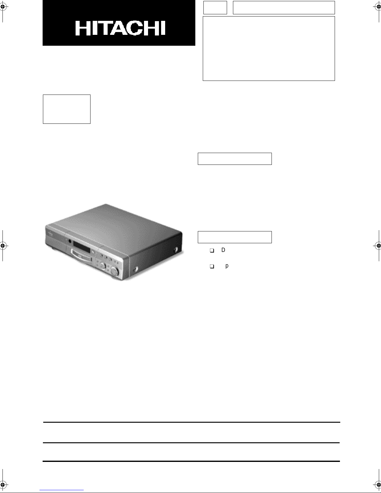
Hitachi DV-P250U, DV-P250E/UK, DV-P250A, DV-P250A/M, DV-P250A/S Service Manual
...
TK NO. 9901E
DV-P250U/(PX)
DV-P250E/(UK)
SERVICE MANUAL
Please carefully read this guide before using the device. The Hitachi DVD Player has been designed to
ADVICE
prevent fire, electrical shock, injury , or harmful radiation. It has been legally f abricated in accordance with
the Electrical Appliances Act. Therefore, when using the device, please follow advice in this service
guide to keep it safe to use.
DV-P250A/(M)/(S)/(AU)
DV-P250C
1. In brief
DV-P250 is a device for DVD playback.
This device is to be used by connecting it to the
video input terminal of a TV set.
2. Features
Disc navigation system facilitates program
T
search.
Speedy operation by 2x speed drive.
T
SPECIFICATIONS AND PARTS ARE SUBJECT TO CHANGE FOR IMPROVEMENT.
July 1999 Digital Media Products Division, Tokai
DVD PLAYER
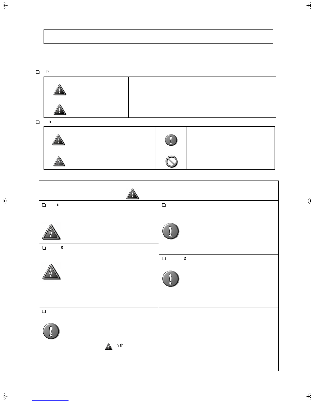
PRECAUTIONS FOR SAFETY
(Please follow.)
Before undertaking repair work, please read through this [Precautions for safety].
The following points should be observed in order to prevent accidents from happening and to ensure the
safety of the device.
Degrees of danger or damage that can be caused b y faulty operation are indicated by the following marks:
WARNING
CAUTION
The following marks identify actions to be taken:
This mark indicates items to which ‘You
should pay attention’.
This ma rk indicates: ‘You should be cautious of electric shock ’.
You should pay attention.
Where a specia l attention is required, it is
indicated by a label or stamp. For example, on
the cabinet, chassis, or parts.
Please respect the indicat ed items and the
‘Precautions for use’ of the manual.
You should be cautious against electric shock.
Please be careful during operations because
there are high voltage and recharging parts
insid e. An electric shock or death may happ en
by touching them.
When disa ssembl ing , assem bling, or repl acin g
a part, the power plug has to be pulled off.
Touching by error a powered part may cause
an electric shock, death, or injury.
Please use designat ed parts.
Parts are characterized by uninflammability
and voltage resistance. Therefore, parts
having these same characteristics must be
used in replacemen t.
Especially for parts important in insuring
safety, identified by in the schematic or
parts list, a part wit h the identical part number
shall be used.
If a pa rt with a different part number is used,
an electric shock or a fire may occur.
Under t his mark, there is “Possible death or serious injury”.
Under this mark, there is “Possible injury or material damage”.
This mark indicates items ‘You have to
accomplish’.
This ma rk indicates ‘Forbidden items’.
WARNING
The original part installat ion and wiring route
shall be restored.
For safety, some parts are insulated by a tube
or a tape, or installed without contact with
substrate. The internal wi ring is kept a
distance from hot or high voltage parts by
clamps or rout ing. Please restore them as
init ially do ne to prevent e lectric shock o r fire
from happ en in g.
Please check safety after servicing.
Please ch ec k if di smoun t ed screw s , p art s, and
wires are reinstall ed as bef ore and if the ar ea
surrounding the repair is damaged.
Please also measure insulation resistance with
a ohmmeter and to confirm th at it is more than
20MΩ.
There is risk of electric shock or fire if the
insul ation resistan ce is less than 20MΩ.
II

Table Of Contents
Chapter 1 System Introduction
System Specification . . . . . . . . . . . . . . . . . . . . . . . . . . . . . . . . . . . . . . . . . . . . . . . . . . .1
Hitachi DV-P250E . . . . . . . . . . . . . . . . . . . . . . . . . . . . . . . . . . . . . . . . . . . . . . . . .1
Hitachi DV-P250U/DV-P250A/DV-P250C . . . . . . . . . . . . . . . . . . . . . . . . . . . . . . .2
ACER DVD-5500/DVD-5300 . . . . . . . . . . . . . . . . . . . . . . . . . . . . . . . . . . . . . . . . .3
ACER DVD-5100 . . . . . . . . . . . . . . . . . . . . . . . . . . . . . . . . . . . . . . . . . . . . . . . . . .4
System Outlook . . . . . . . . . . . . . . . . . . . . . . . . . . . . . . . . . . . . . . . . . . . . . . . . . . . . . . .5
Front Panel . . . . . . . . . . . . . . . . . . . . . . . . . . . . . . . . . . . . . . . . . . . . . . . . . . . . . .5
Rear Panel. . . . . . . . . . . . . . . . . . . . . . . . . . . . . . . . . . . . . . . . . . . . . . . . . . . . . . .6
Description of adopted new technology. . . . . . . . . . . . . . . . . . . . . . . . . . . . . . . . . . . . .9
Digital signal circuit . . . . . . . . . . . . . . . . . . . . . . . . . . . . . . . . . . . . . . . . . . . . . . . .9
Video circuit (DEC substrate). . . . . . . . . . . . . . . . . . . . . . . . . . . . . . . . . . . . . . . .10
VIDEO OUTPUT CIRCUIT (RJK substrate) . . . . . . . . . . . . . . . . . . . . . . . . . . . .13
AUDIO CIRCUIT . . . . . . . . . . . . . . . . . . . . . . . . . . . . . . . . . . . . . . . . . . . . . . . . .13
KARAOKE CIRCUIT . . . . . . . . . . . . . . . . . . . . . . . . . . . . . . . . . . . . . . . . . . . . . .16
FRONT (FSW) SUBSTRATE CIRCUIT. . . . . . . . . . . . . . . . . . . . . . . . . . . . . . . .18
POWER SUPPLY CIRCUIT. . . . . . . . . . . . . . . . . . . . . . . . . . . . . . . . . . . . . . . . .18
CLOCK CIRCUITS. . . . . . . . . . . . . . . . . . . . . . . . . . . . . . . . . . . . . . . . . . . . . . . .19
Troubleshooting. . . . . . . . . . . . . . . . . . . . . . . . . . . . . . . . . . . . . . . . . . . . . . . . . . . . . .22
VIDEO CIRCUIT . . . . . . . . . . . . . . . . . . . . . . . . . . . . . . . . . . . . . . . . . . . . . . . . .22
AUDIO CIRCUIT . . . . . . . . . . . . . . . . . . . . . . . . . . . . . . . . . . . . . . . . . . . . . . . . .23
KARAOKE CIRCUIT . . . . . . . . . . . . . . . . . . . . . . . . . . . . . . . . . . . . . . . . . . . . . .24
About System Reset Function . . . . . . . . . . . . . . . . . . . . . . . . . . . . . . . . . . . . . . .25
System Utility . . . . . . . . . . . . . . . . . . . . . . . . . . . . . . . . . . . . . . . . . . . . . . . . . . . .25
Chapter 2 Removal and Replacement
Prelimaries before disassembling machines . . . . . . . . . . . . . . . . . . . . . . . . . . . . . . . .27
Before You Begin. . . . . . . . . . . . . . . . . . . . . . . . . . . . . . . . . . . . . . . . . . . . . . . . .27
Disassembly Procedures. . . . . . . . . . . . . . . . . . . . . . . . . . . . . . . . . . . . . . . . . . . . . . .29
Removing the Top Cover . . . . . . . . . . . . . . . . . . . . . . . . . . . . . . . . . . . . . . . . . . .29
Removing the FootStand . . . . . . . . . . . . . . . . . . . . . . . . . . . . . . . . . . . . . . . . . . .29
Removing the Front Panel . . . . . . . . . . . . . . . . . . . . . . . . . . . . . . . . . . . . . . . . . .30
Removing the MPEG Control Board . . . . . . . . . . . . . . . . . . . . . . . . . . . . . . . . . .31
Removing the Power Supply Board. . . . . . . . . . . . . . . . . . . . . . . . . . . . . . . . . . .32
Removing the DVD-ROM Drive . . . . . . . . . . . . . . . . . . . . . . . . . . . . . . . . . . . . . .32
Removing the Outlet Board . . . . . . . . . . . . . . . . . . . . . . . . . . . . . . . . . . . . . . . . .33
Removing the Front Panel Control Boards . . . . . . . . . . . . . . . . . . . . . . . . . . . . .34
Connector Setting . . . . . . . . . . . . . . . . . . . . . . . . . . . . . . . . . . . . . . . . . . . . . . . . . . . .36
Appendix A Schematics
DEC Board (A side) . . . . . . . . . . . . . . . . . . . . . . . . . . . . . . . . . . . . . . . . . . . . . . . . . . .37
DEC Board (B side) . . . . . . . . . . . . . . . . . . . . . . . . . . . . . . . . . . . . . . . . . . . . . . . . . . .38
RJK Board (A side) . . . . . . . . . . . . . . . . . . . . . . . . . . . . . . . . . . . . . . . . . . . . . . . . . . .39
RJK Board (B side) . . . . . . . . . . . . . . . . . . . . . . . . . . . . . . . . . . . . . . . . . . . . . . . . . . .40
FSW/MVR/FJK Board (A side) . . . . . . . . . . . . . . . . . . . . . . . . . . . . . . . . . . . . . . . . . .41
FSW/MVR/FJK Board (B side) . . . . . . . . . . . . . . . . . . . . . . . . . . . . . . . . . . . . . . . . . .42
System Block Diagrams. . . . . . . . . . . . . . . . . . . . . . . . . . . . . . . . . . . . . . . . . . . . . . . .43
Exploded Diagram . . . . . . . . . . . . . . . . . . . . . . . . . . . . . . . . . . . . . . . . . . . . . . . . . . . .44
Replacement Parts List (DV-P250) . . . . . . . . . . . . . . . . . . . . . . . . . . . . . . . . . . . . . . .45
III
Chapter 1
System Introduction
System Specification
Hitachi DV-P250E
Specification
General Model....................................................................................................................DV-P250E
Operating laser.........Semi-conductor laser : Wave length 650nm(DVD) / 780nm(CD,VCD)
Power supply................................................................................................. AC230V, 50Hz
Power consumption........................................................................................................27W
Weight..........................................................................................................................3.9 Kg
Overall size...........................................................................434 (W) x 315 (D) x 98 (H) mm
Allowable operating temperature.....................................................................+5°C~+35°C
Allowable operating humidity......................................................15~75% (no condensation)
AV connector output
terminal
S Video output terminal Y output level.....................................................................................................1Vp-p (75Ω)
Video output Output level........................................................1 Vp-p (synchronous when loaded at 75Ω)
Audio output Output level....................................................................................200mVrms (1KHz, -20dB)
Other terminals Digital audio output optical/coaxial..........................................................Coaxial terminal : 1
Accessories Remote control unit..............................................................................................................1
AV connector output....................................................................................21-pin connector
This connector provides the video and signals for connection to a color video TV monitor (or
TV set) which has an ‘AV CONNECTOR’ terminal.
C output level.................................................................................NTSC : 0.286Vp-p (75Ω)
...............................................................................................................PAL : 0.3Vp-p (75Ω)
Output terminal......................................................................................................S terminal
Output terminal..........................................................................................................pin jack
Analog audio output...........................................................................2 system (pin jack x 4)
Sound characteristics :
Frequency characteristics............................................................CD : 4Hz~20KHz (EIAJ)
....................................................................................DVD : 4Hz~22KHz (48K sampling)
...............................................................................................4Hz~44KHz (96K sampling)
SN ratio...................................................................................................................110 dB
Dynamic range.........................................................................................................100dB
Total harmonic distortion rate.................................................................................0.003%
Wow fluttertics.............................Measurement limit less than (±0.001% W.PEAK)(EIAJ)
(DTS/AC-3/MPEG2, AC3, LPCM, OFF commutable).......................Optical connector : 1
Single ‘AAA’ battery..............................................................................................................2
AV cord.................................................................................................................................1
Power cord...........................................................................................................................1
Chapter 1 1
Hitachi DV-P250U/DV-P250A/DV-P250C
Specification
General Model................................................................................DV-P250U/DV-P250A/DV-P250C
Operating laser.........Semi-conductor laser : Wave length 650nm(DVD) / 780nm(CD,VCD)
Power supply.............................................................................DV-P250U : AC120V, 60Hz
........................................DV-P250U (PX), DV-P250A, DV-P250C : AC110-240V, 50/60 Hz
Power consumption........................................................................................................27W
Weight..........................................................................................................................3.9 Kg
Overall size...........................................................................434 (W) x 315 (D) x 98 (H) mm
Allowable operating temperature.....................................................................+5°C~+35°C
Allowable operating humidity......................................................15~75% (no condensation)
Component output terminal Y output level....................................................................................................1 Vp-p (75Ω)
output level..................................................................................NTSC : 0.7 Vp-p (75Ω)
P
B
..........................................................................................................PAL : 0.698 Vp-p (75Ω)
output level..................................................................................NTSC : 0.7 Vp-p (75Ω)
P
R
..........................................................................................................PAL : 0.698 Vp-p (75Ω)
Output terminal..........................................................................................................pin jack
S Video output terminal Y output level.....................................................................................................1Vp-p (75Ω)
C output level.................................................................................NTSC : 0.286Vp-p (75Ω)
...............................................................................................................PAL : 0.3Vp-p (75Ω)
Output terminal......................................................................................................S terminal
Video output Output level........................................................1 Vp-p (synchronous when loaded at 75Ω)
output terminal...........................................................................................................pin jack
Audio output Output level....................................................................................200mVrms (1KHz, -20dB)
Mixed 2ch output................................................................................1 system (pin jack x 2)
5.1ch output.......................................................................................1 system (pin jack x 6)
Sound characteristics :
Frequency characteristics............................................................CD : 4Hz~20KHz (EIAJ)
....................................................................................DVD : 4Hz~22KHz (48K sampling)
...............................................................................................4Hz~44KHz (96K sampling)
SN ratio...................................................................................................................110 dB
Dynamic range.........................................................................................................100dB
Total harmonic distortion rate.................................................................................0.003%
Wow/flutter .................................Measurement limit less than (±0.001% W.PEAK)(EIAJ)
Other terminals Digital audio output optical/coaxial..........................................................Coaxial terminal : 1
(DTS/AC-3/MPEG2, LPCM, OFF commutable)................................Optical connector : 1
Accessories Remote control unit..............................................................................................................1
Single ‘AAA’ battery..............................................................................................................2
AV cord.................................................................................................................................1
Power cord...........................................................................................................................1
AC socket (DV-P250U (PX) only)........................................................................................1
2 Chapter 1
ACER DVD-5500/DVD-5300
Specification
General Model..................................................................................................DVD-5500/DVD-5300
Operating laser.........Semi-conductor laser : Wave length 650nm(DVD) / 780nm(CD,VCD)
Power supply.......................................................Taiwan : DVD-5500/5300 : AC120V, 60Hz
.........................................................Hong Kong : DVD-5500/5300 : AC110-240V, 50/60 Hz
Power consumption........................................................................................................27W
Weight..........................................................................................................................3.9 Kg
Overall size...........................................................................434 (W) x 315 (D) x 98 (H) mm
Allowable operating temperature.....................................................................+5°C~+35°C
Allowable operating humidity......................................................15~75% (no condensation)
Component output terminal
(DVD-5500 only)
S2 Video output terminal Y output level.....................................................................................................1Vp-p (75Ω)
Video output Output level........................................................1 Vp-p (synchronous when loaded at 75Ω)
Audio output Output level....................................................................................200mVrms (1KHz, -20dB)
Other terminals Digital audio output optical/coaxial..........................................................Coaxial terminal : 1
Accessories Remote control unit..............................................................................................................1
Y output level....................................................................................................1 Vp-p (75Ω)
output level..................................................................................NTSC : 0.7 Vp-p (75Ω)
P
B
..........................................................................................................PAL : 0.698 Vp-p (75Ω)
output level..................................................................................NTSC : 0.7 Vp-p (75Ω)
P
R
..........................................................................................................PAL : 0.698 Vp-p (75Ω)
Output terminal..........................................................................................................pin jack
C output level.................................................................................NTSC : 0.286Vp-p (75Ω)
...............................................................................................................PAL : 0.3Vp-p (75Ω)
Output terminal......................................................................................................S terminal
(DVD-5500 S terminal x 2)
output terminal...........................................................................................................pin jack
(DVD-5500 pin jack x 2)
Mixed 2ch output................................................................................1 system (pin jack x 2)
5.1ch output.......................................................................................1 system (pin jack x 6)
Sound characteristics :
Frequency characteristics............................................................CD : 4Hz~20KHz (EIAJ)
....................................................................................DVD : 4Hz~22KHz (48K sampling)
...............................................................................................4Hz~44KHz (96K sampling)
SN ratio...................................................................................................................110 dB
Dynamic range.........................................................................................................100dB
Total harmonic distortion rate.................................................................................0.003%
Wow/flutter...................................Measurement limit less than (±0.001% W.PEAK)(EIAJ)
(DTS/AC-3/MPEG2, LPCM, OFF commutable)................................Optical connector : 1
Single ‘AAA’ battery..............................................................................................................2
AV cord.................................................................................................................................1
Power cord...........................................................................................................................1
Chapter 1 3
ACER DVD-5100
Specification
General Model....................................................................................................................DVD-5100
Operating laser.........Semi-conductor laser : Wave length 650nm(DVD) / 780nm(CD,VCD)
Power supply................................................................................................. AC120V, 60Hz
Power consumption........................................................................................................27W
Weight..........................................................................................................................3.9 Kg
Overall size...........................................................................434 (W) x 315 (D) x 98 (H) mm
Allowable operating temperature.....................................................................+5°C~+35°C
Allowable operating humidity......................................................15~75% (no condensation)
S Video output terminal Y output level.....................................................................................................1Vp-p (75Ω)
C output level.................................................................................NTSC : 0.286Vp-p (75Ω)
...............................................................................................................PAL : 0.3Vp-p (75Ω)
Output terminal......................................................................................................S terminal
Video output Output level........................................................1 Vp-p (synchronous when loaded at 75Ω)
output terminal...........................................................................................................pin jack
Audio output Output level....................................................................................200mVrms (1KHz, -20dB)
Analog audio output...........................................................................2 system (pin jack x 4)
Sound characteristics :
Frequency characteristics............................................................CD : 4Hz~20KHz (EIAJ)
....................................................................................DVD : 4Hz~22KHz (48K sampling)
...............................................................................................4Hz~44KHz (96K sampling)
SN ratio...................................................................................................................110 dB
Dynamic range.........................................................................................................100dB
Total harmonic distortion rate.................................................................................0.003%
Wow fluttertics.............................Measurement limit less than (±0.001% W.PEAK)(EIAJ)
Other terminals Digital audio output optical/coaxial..........................................................Coaxial terminal : 1
(DTS/AC-3/MPEG2, LPCM, OFF commutable)
Accessories Remote control unit..............................................................................................................1
Single ‘AAA’ battery..............................................................................................................2
AV cord.................................................................................................................................1
Power cord...........................................................................................................................1
4 Chapter 1
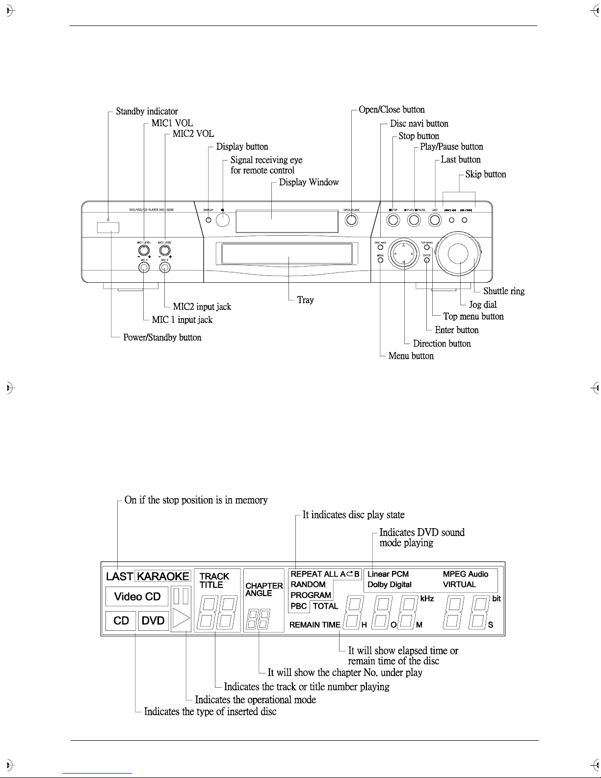
System Outlook
Front Panel
NOTE: The Karaoke functions (includes MIC1 VOL/MIC2 VOL/MIC1 input jack/M IC2 input jack) are only
available at Acer DVD-5500 and DVD-5300 models.
NOTE: The Jog dial and Shuttle ring functions are only available at Acer DVD-5500 and Hitachi DV-P250
models.
Display Wind ow
Chapter 1 5
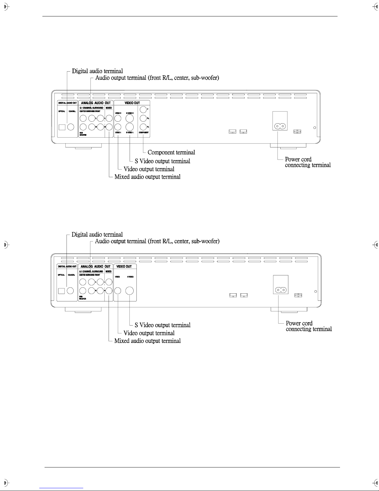
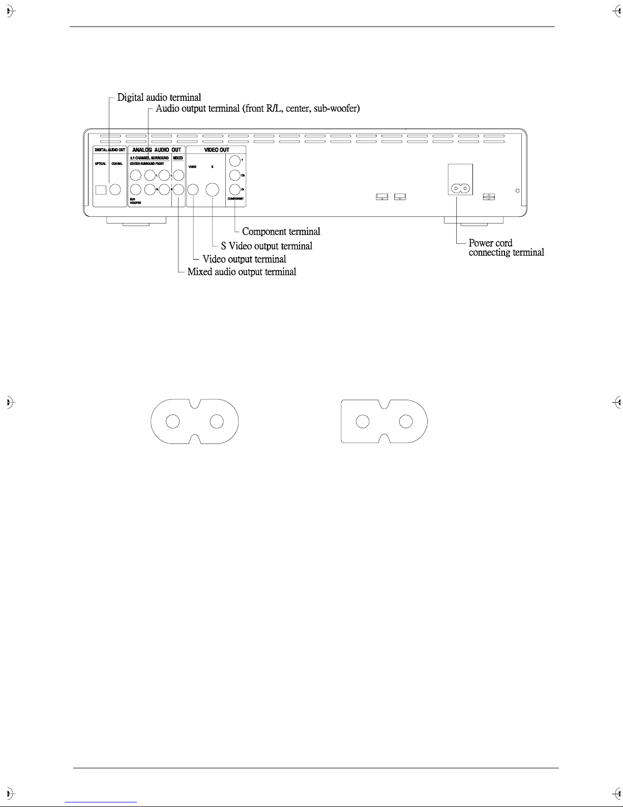
Rear Panel
ACER DVD-5500
ACER DVD-5300
6 Chapter 1
Acer DVD-5100
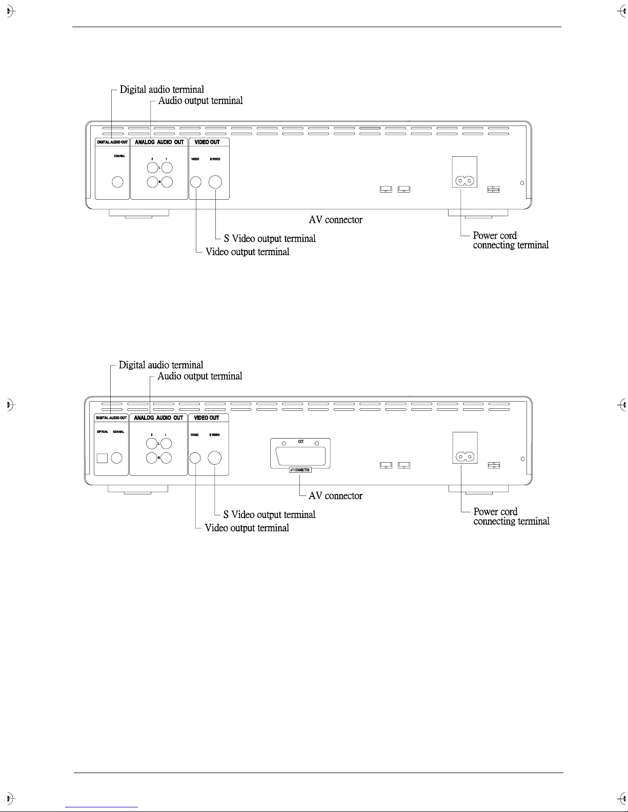
Hitachi DV-P250E
Chapter 1 7
Hitachi DV-P250U/DV-P250A/DV-P250C
NOTE: For the different voltages of each area, the power connector has the following two types. The Power
Connector type 2 is only for the areas of Taiwan and U.S.A. model. And the power connector type 1 is
for the DV-P250U(PX) and other s.
Power Connector type 1
Power Connector type 2
8 Chapter 1
Description of adopted new technolo g y
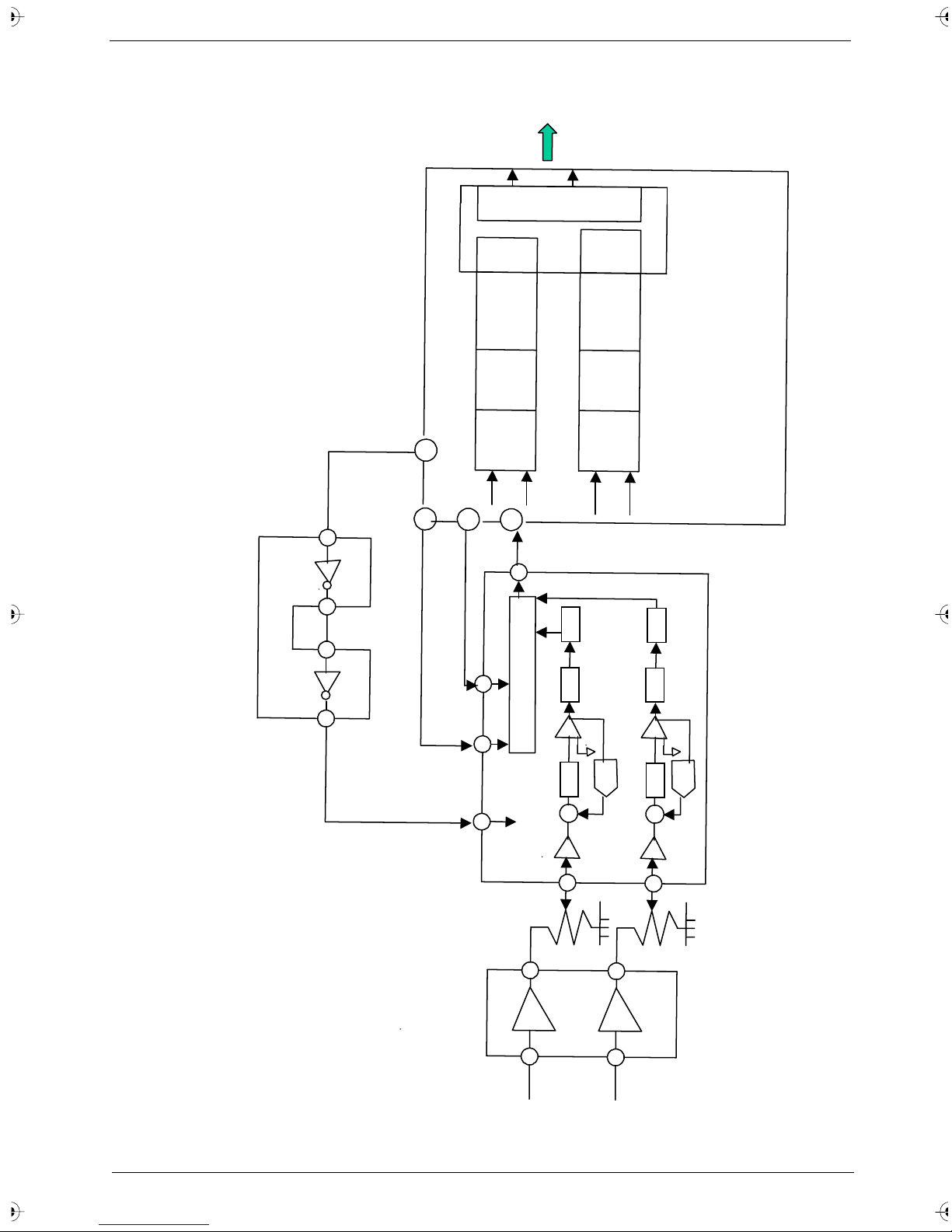
Digital signal circuit
Data Flow
The following figure shows the block diagram of digital signal circuit.
DVD ROM
DRIVE
PG1101
20 MHz X'TAL
X1601
SH MICOM
IC1601
TRACK BUFFER
4Mbit
IC1603
FLASH MEMORY
8Mbit
IC1602
I/F GATE ARRAY
IC1101
27 MHz X'TAL
X2203
The disc data will be read by DVD ROM Drive then pass through I/F gate array (IC1101). The read data will
then be stored in th e tr ack buffer by SH MICOM(IC1601). Then the stored dat a will be read out fro m the track
buffer in response to the demand by A/V decoder (IC1201) and input in A/V decod er through I/F gate array.
Finally, the A/V decoder will demodulate/ decode the data accor ding to their contents and output audio dat a to
Audio DAC (IC1501~1504), and video data to Vi deo encoder (IC2202)
SH BUS
A/V DECODER
IC1201
BUFFER RAM
16Mbit x 2 SDRAM
IC2203~IC2204
To Audio DAC
To VIDEO ENCODER
Reference Clock of each IC
IC Reference Clock
IC1101 I/F GATE ARRAY 20MHz clock generated by SH MICOM
IC1601 SH MICOM System clock of X1601 20MHz X'TAL, SH
IC1602 FLASH MEMORY Nil (Control signal is generated by SH MICO M)
IC1603 TRACK BU FFER Nil (Control signal is generat ed by SH MICOM)
IC1201A/V DECODER System clock and video interface clock are input from X22 03 27M Hz X'TAL.
Chapter 1 9
Audio interface clock is out put from 169 pin named DA-XCK.
Functions of each IC
No. IC Function s
1 IC1101 I/F GATE ARRAY Execute data transfer timings from ATAPI to track buffer,
and from track buffer to A/V decoder.
2 IC1601 SH MICO M Execute data transfer, presetting and cont rol of each IC. 5V
3 IC16 02 FLASH MEMO RY Store memory for SH MICOM software 5V
4 IC1603 TRACK BUFFER Buffer memory for data transfer 5V
5 IC1201 A/V DECODER Execute decompression (decoding) of data compressed by
MPEG
6
IC2203~IC2204 BUFFER RAM
Memory used for decompression (decoding) of data
compre ssed by MPEG and controlled by A/V decoder
Operating
5V
3.3V
3.3V
The following is th e description of the fun ctions of each IC:
1. I/F GATE ARRA Y (I C1101)
It executes signal timing changes between SH MICOM (IC1601), DVD ROM drive I/F (PG1101), and A/V
decoder (IC1201). It operates on 20MHz cl ock which is an output from SH MICOM.
2. SH MICOM (IC1601)
It transfe rs dat a and executes presetting and control of each IC.
Data transfe r from DVD ROM drive I/F is done b y set ting a regist er of I/F gat e array and by i nter mediary o f
I/F gate array.
In addition, it controls audio DAC ((IC1501~I C1 504) and video encoder (IC2202), manages tr ack buffer
(IC1603) and fl ash m emory (IC1602), and communi cates with FL MICOM (IC1701).
With 20MHz XTAL(X1601) attached it pulses and is used as a syst em clock.
3. FLASH MEMORY (IC1602)
A 8Mbits flash memory is used. It stores SH MICOM program and its access is controlled by SH MICOM.
4. TRACK BUFFER (IC1603)
A 4Mbit DRAM is used. It stores data read out from disc. Its control is done by SH MICOM , and its data is
read-written vi a I/F gate array. In addition a par t of t his buffer is used as the work area of SH MICOM.
5. A/V DECODER (IC1201)
Data input from track buffer via I/F gate array is separated into audio data and video data. MPEG
compressed data are decompressed (decoded) and output as digit al video and digital audio (AC-3). SH
MICOM controls it via I/F gate array. System clock, clock of video interface signals, and clock of audio
interface signals operate by inputting 27MHz respecti vely.
6. BUFFER SDRAM (IC2203~IC2204)
Two 16 Mbit s SDRAM are used. A/V decoder control s it and it is used to decompr ess audio and video
data compress ed by MPEG.
Voltage
Video circuit (DEC substrate)
8bit YCRCB digital video stream (P) output from A/V decoder are input to video encoder
ADV7172(IC2202). Video encoder is preset in master mode that generates reference signals and
receives 27MHz from system clock X2203 and outputs H,V synchro nous signals to A/V decoder.
By presetting of internal register, video encoder generates:
1. NTSC (North America, Japan, Taiwan)
2. PAL (Europe, Asia)
standard analog video signals.
10 Chapter 1

Filter circuit eliminate s high frequency componen ts of analog video signal s output from video encoder.
Afterwards in S2 processor circ uit DC volt age is superp osed on C signals then outp ut 3 types of vi deo signal s:
composite video signals, Y/C(S2) video signals and YP
/RGB to RJK substrate via 17P connector
BPR
(PG2201).
The following is a description of video cir cuit along signal f low:
Block Diagram of VIDEO ENCODER B1865A (IC2202) interior
P
(2~9)
MULTIPLEXER
SECTOR
UPSAMPLE
CONVERTER
CONVERTER
CLK
(48)
RESET
SECTOR
Y
CB/C
R
(44)
BLANK
(16)
SDA/SDL
(21,20)
I2C
INTERFACE
SYNC
ADDER
BURST
ADDER
H/V SYNC OUT
I2C BUS
ENCODER SECTOR
MACROVISION
(14/15)
CLOSED
CAPTION
CGMSDEMULTIPLEXER
CHROMA
ENCODER
Y/C MIX
VOLTAGE REFERENCE
(22/23/36/37/38)
C (29)
CVBS (35)
DAC
D/A
CONVERTER
SECTOR
Y/G (28)
PB/B (25)
Y (33)
PR/R (24)
VIDEO ENCODER ADV7172 (IC2202)
1. MULTIPLEXER SECTOR
It transfo rms input digital video stream (Input at 2~9 pins) in 8bit parallel data then separates them in Y
data and C
2. CONVERTER SECTOR
It generates various internal ti m ing signals with the sy nchronous signal as standard by adding
synchronous si gnal s gener ated i n IC to Y dat a, accordi ng to t he c onditions set in the inter nal re gister or by
adding BURST signals to C
decoder (Ou tput at 14,15 pi ns). In addi tion, when power is turned ON, RESET sign al (I nput of L level at 44
pin) is input to res et the register in IC.
Moreover, writing in the internal register (presetti ng) is done via I2C BUS ( 20,21 pins).
3. ENCODER SECTOR
The followi ng 1~3 data are inse rted in VIDEO DATA according to preset conditions in the i nternal register:
a. Closed caption
NTSC Mode: 21 lines and 284 lines/ PAL Mode: 22 lines and 335 ines.
b. CGMS (Copy Guard Management System)
20 lines and 280 lin es of NTSC.
c. Macrovision Copy Prevention System
Finally it generates DIGITA L INTENSITY DA TA, DIGITAL CHROMA DATA, and DIGITAL
COMPOSITE DATA.
data and changes simultaneously the rate (6.75MB/S->13.5MB/S).
B/CR
B/CR
data. At the same time it outputs these synchronous signals to A/V
Chapter 1 11
4. D/A CONVERTER (DAC)SECTOR
Constituted of 10bit DAC, it t ransfo rms DIGITAL VIDEO DATA to ANALOG VIDEO DA TA for output. Under
control of output voltage by DAC pins (22, 23, 36, 37, 38 pins), it output 3 kinds of ANALOG VIDEO
SIGNALS:
a. ANALOG COMPOSITE VIDEO SIGNALS (CVBS/35 pin), output voltage 1. 0Vpp.
b. ANALOG INTENSITY SIGNALS (Y/33 pin), output voltage 1.0Vpp.
c. ANALOG CHROMA SIGNALS (C/29 pin), BURST part output voltage 286mVpp.
d. ANALOG COMPONENT YP
BPR
/RGB.
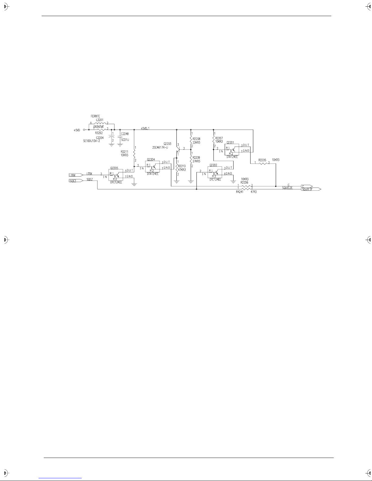
S2 Processing Circuit (only for Japan)
S2 is a standard used in wide tel evision sets possessing screen size swit ching function in NTSC mode. By
inputting VIDEO signals formed by superposing DC voltage on C signal at S input terminal, it switches
automatically to TV display size. The DC voltage superposed on C signal varies according to the ASPECT
RATIO of VIDEO SIGNALS.
1. Case of SQUEEZE SIGNAL (*1)
H-level voltage is in put in SQUEEZE INPUT; Q2202 and Q2201 a re power ed and +4V DC volt age is superpos ed
on C signal output line.
2. Case of LETTER BOX SIGNAL (*2)
H-level voltage is input in LETTER INPUT; Q2205, Q2204, and Q2203 are powered and +1.8V DC voltage is
superposed on C signal output line.
1. *1: It is a laterally shrunk image information with 525 lines and an aspect ratio of 16:9 car ried by the
standard TV signal format of 525 lines and an aspec t rat io of 4:3. When vi ewing on a 4:3 TV s et, t he imag e
appears vertically oblong.
2. *2: It is a wide screen si gnal in the standard TV sign al f ormat of 525 lines and an aspect ra ti o of 4:3 with
coexistence of upper and lower blank are as of 525 l ines and an aspect ratio of 4: 3 screen and the
principal image area of 4:3 aspect ratio (line 53~232/316~495). When viewing on a 4:3 TV set, one sees
black areas at the top and bot tom of the screen.
12 Chapter 1
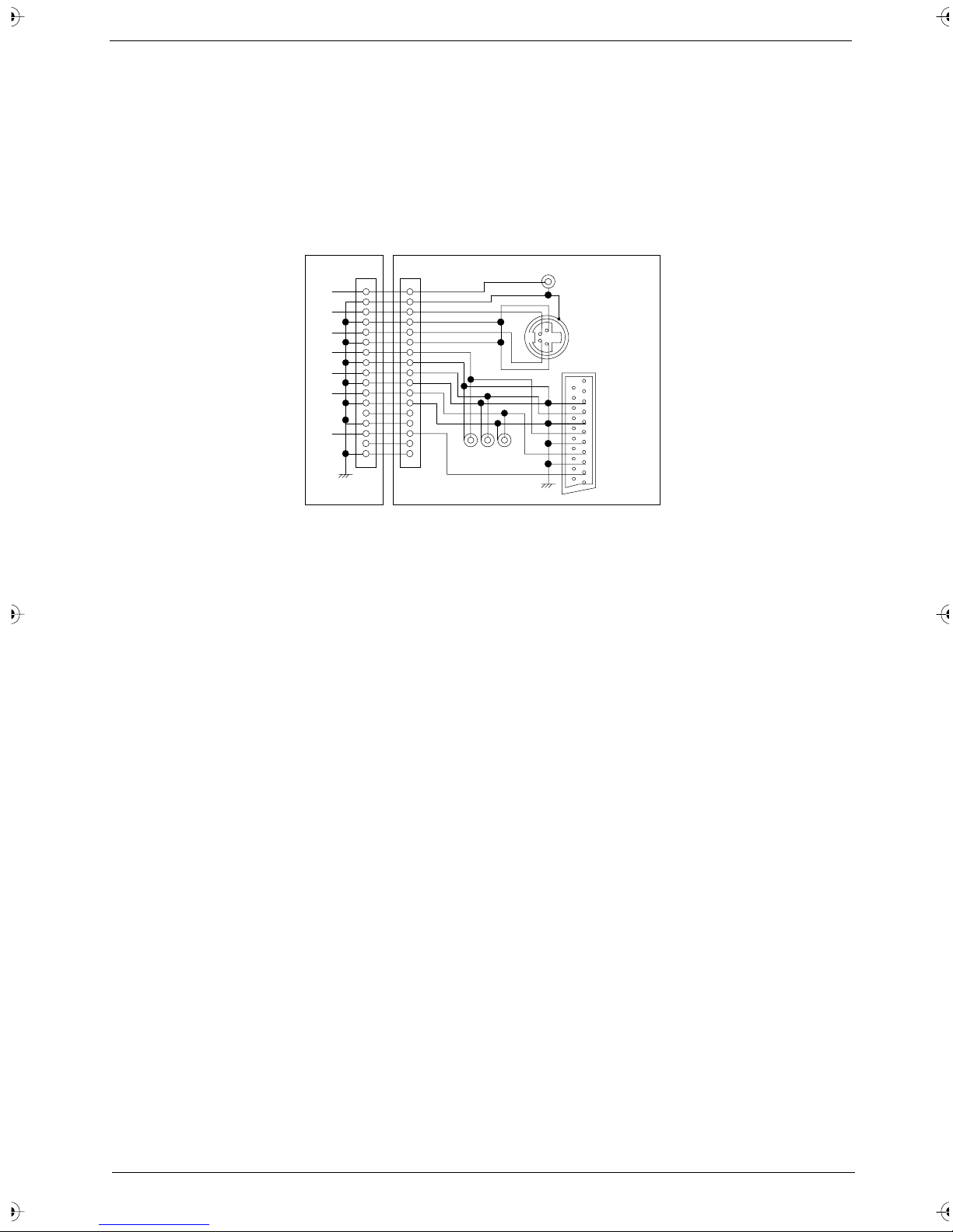
VIDEO OUTPUT CIRCUIT (RJK substrate)
Analog composite video signals (CVBS), analog intensity signals (Y), analog chroma signals (C) and analog
component si gnals (YP
BPR/RGB)
connector (PG2201~CN1302). From RJK substrate, CVBS signals are output fr om output terminal J13 07 and
Y/C signals are output from output terminal J1302. Component signals are output from output terminal J1306
(YP
) or J1361 (RGB).
BPR
DEC Substrate RJK Substrate
are sent from DEC substr ate to RJK substrate by passi ng through 17P
PG2201 PG1302
J1307
VIDEO
J1302
S
J1361
J1306
COMPONENT
SCART
AUDIO CIRCUIT
Audio circuit is shown in page 15.
Audio circui t is composed of D/A convert er secto r (DEC substr ate) that transf orms digi tal audio sig nals outpu t from
A/V decoder (I C1201 ), analog pro cessing sect or (RJ K subs trat e) that consi sts of an o perati onal ampl ifi er, and mute
circuit (DEC substrate, RJK substrate) for stopping audio output when required.
1. D/A CONVERTER SECTOR (DEC substrate)
D/A converter sec tor is composed of IC1502 that receives and transforms digital audio signals from A/V
decoder in analog signals.
IC1502 is a converter corresponding to FL and FR signals of sampling frequencies 44.1/48/96KHz and
data lengths16/20/24bit, and digital audio signal s from A/V decoder is input at pin 2.
To these digital audio signa ls are i nserte d FL and FR si gnals in time sh aring mode . When t hey are i nput in
pin 1, they are separ ated in FL and FR signals by R clock and after transformati on analog FL signals are
output at pin 16 and FR signals at pin 13. Moreover, when there are no input signals at pin 2, a signal
called ZERO MUTE is output to pin 21 to mute useless nois es (See paragraph on MUTE CIRCUIT.)
Every functi ons of IC1502 is preset by MICOM and con tr olling signals from SH MICOM are input at pins
26, 27,and 28. As for preset ting items, there are data length, sampl ing frequency, signal polarity, and deemphasis.
2. ANALOG PROCESSING SECTOR (RJK substrate)
Analog processing sector is composed of operational ampli fier IC1508 that is a fil ter and operational
amplifier IC1510 that amplifies audio signals.
Filter portion is composed of RC low pass filter and IC1 508 formed active low pass filter and ther e are 3
sections. The diagram below shows its filter portion circuit (for FL signals only).
Chapter 1 13
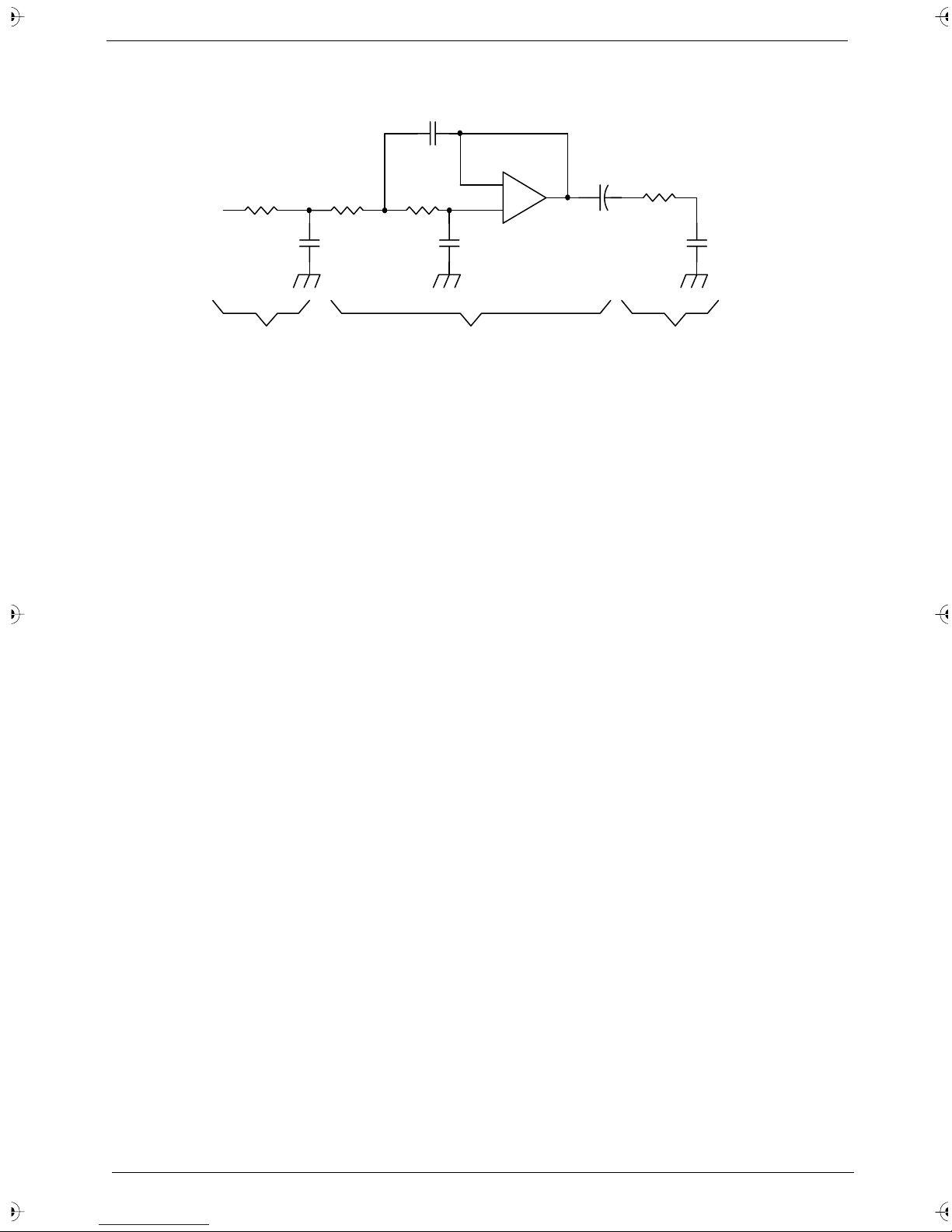
C1561
R1527
R1529
R1531
2
3
1
+
R1533
+
-
C1567
C1559
IC1508
C1563
C1571
Filter 2Filter 1 Filter 3
This 3-secti on fi lter constitutes a low pass filter of ov eral l cutoff frequency of 44KHz. Audio signals after
low pass filter is amplified by IC1510 by about 6dB and output to audio out1 and audio out2.
Here, amon g audio signals, FL signals are input at pin 3 of I C1508 and ou tput from p in 1, then input to pin
2 of IC1510 then output from pin 1.
FR signals are inpu t at pin 5 of IC1508 and output from pin 7, t hen input to pin 6 of IC1510 then output
from pin 7.
3. MUTE CIRCUIT (DEC substrate, RJK substrate)
The principal rol e of mute circuit is the erasing of useless noises occurring when power is turned on.
Mute signal for noise erasing is generat ed by SH MICOM, reverse-amplifi ed by Q 1505 and Q1506. Then
by putting Q1310 and Q1311 'ON', it mutes audio signals.
In addition, if IC1502 detects no-signal, it generate a mute signal called ZERO MUTE. This latter is
reverse-amplified by Q1507 and mutes useless audio signals by putting Q1310 and Q1311 'ON'.
14 Chapter 1
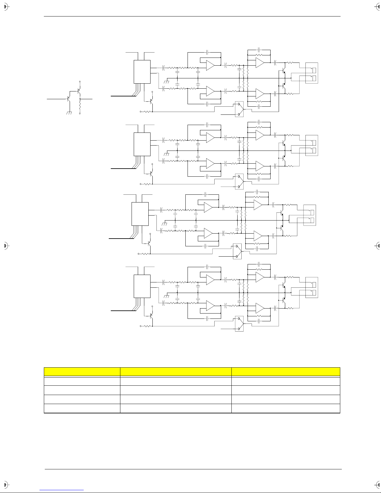
FROM SH u-COM
+5V_STBY
2
1
Q1505
3
-8V
1
Q1506
3
A MUTE
LR CLOCK DIGITAL AUDIO SIGNAL
1
LRCIN
IC1501
D/A CONVERTER
MDMCML
262728
FROM SH u-COM
-8V
LR CLOCK DIGITAL AUDIO SIGNAL
1
LRCIN
IC1502
D/A CONVERTER
MDMCML
262728
FROM SH u-COM
-8V
LR CLOCK DIGITAL AUDIO SIGNAL
1
LRCIN
VOUTL
IC1503
D/A CONVERTER
VOUTR
MDMCML
262728
FROM SH u-COM
-8V
LR CLOCK DIGITAL AUDIO SIGNAL
1
LRCIN
IC1504
D/A CONVERTER
MDMCML
262728
FROM SH u-COM
-8V
2
DIN
VOUTL
VOUTR
ZERO
21
2
2
DIN
VOUTL
VOUTR
ZERO
21
2
2
DIN
ZERO
21
2
2
DIN
VOUTL
VOUTR
ZERO
21
2
16
13
+5VAU
1
Q1501
3
DTA124EKA
16
13
+5VAU
1
Q1507
3
DTA124EKA
16
13
+5VAU
1
Q1508
3
DTA124EKA
16
13
+5VAU
1
Q1509
3
DTA124EKA
AUDIO CIRCUIT
+
+
+
+
+
+
+
+
IC1507A
2
3
FILTER
5
6
FILTER
IC1508A
2
3
FILTER
5
6
IC1511A
-
2
+
3
FILTER
5
+
6
-
FILTER
IC1513A
2
3
FILTER
5
6
-
+
IC1507B
+
-
-
+
IC1508B
+
-
FILTER
IC1511B
-
+
IC1513B
+
-
FILTER
1
7
1
7
1
7
1
7
+
+
A MUTE
+
+
A MUTE
+
+
A MUTE
+
+
A MUTE
IC1509A
AMP
-
2
+
3
AUDIO MUTE
+
1
Q3503
DOWNMIX-Lch
DOWNMIX-Rch
AMP
1
2
D3301
IC1509B
5
+
7
6
-
3
IC1510A
AMP
-
2
1
+
3
+
AUDIO MUTE
+
Q3504
Q1310
FRONT-Lch
FRONT-Rch
AMP
1
2
D1302
IC1510B
5
+
7
6
-
3
IC1512A
AMP
-
2
1
+
3
+
AUDIO MUTE
+
Q1311
Q1306
SURROUND-Lch
SURROUND-Rch
AMP
IC1512B
5
+
7
6
D1303
1
2
-
3
IC1514A
AMP
-
2
1
+
3
+
+
Q1307
AUDIO MUTE
Q1308
CENTER
WOOFER
AMP
1
2
D1304
IC1514B
5
+
7
6
-
3
Q1309
+
4. 5.1CH Difference List
Output D/A Converter Operational amplifier
Downmix L/R IC 1501 IC 1507, IC 1509
Front L/R IC 1502 IC 1508, IC 1510
Surround L/R IC 1503 IC 1511, IC 1512
Center/Woofer IC 1504 IC 1513, IC 1514
Chapter 1 15

KARAOKE CIRCUIT
(Only available at DVD-5500/DVD-5300 models)
When mic is connected to the mic input terminal, ”KARAOKE” will be lighted on FL tube and mode will be
changed to Karaoke mode. Therefor e, karaoke functions of keycon and vocal cancel may be used. When mic
is disconnected, karaoke mode is ‘OFF’ .
Signals output from MIC1 are input to IC2401 at pi n 5, th en pass through MIC amplifier, and output to MIC
volume RV1762 from pin 7. Afterwards it will be input again to IC2404 at pin 8, then pass through IC2404
internal signal analog/digital converter and output to IC1201 pin 171 from IC2404 pin 1. Similarly signals
output from MIC2 are i nput to IC2401 pin 3, then pass th rough MIC amplifier and output from pin 1 to MIC
volume RV1763. Then input again to IC24 04 pin 5, then pass through IC2404 internal signal analog/digital
converter and output to IC1201 pin 171 fro m IC2404 pin 1,then to MIC1/MIC2 serial data(thr ough IC1201
internal echo/MIC G.ETC signal process) and disc audio L/R signal (through path shift/vocal partnering/audio
G.edc signal process) mix,serial signal output to audio common circuit IC1501 pin 2 and IC1502 pin 2 from
IC1201 pin 161 and IC1201 pin 163.
EXPLAINATION:
1. MCLK(IC2404
2. SCLK(IC2404
3. LRCK(IC2404
4
pin): externa l cl ock input, from IC1201 pin
DVD:384*fs=384*48k=18.432MHz
CD/VCD:384*fs=384*44.1k=16.934MHz
2
pin): MIC audio bit cl ock, from IC1201 pin
DVD:18.432/8=2.304MHz
CD/VCD:16.934/8=2.1168MHz
3
pin): MIC1 and MIC2 L/Rclock, from IC1201 pin 172 to IC2404 pin 3.
DVD:48KHz
CD/VCD:44.1KHz
169
through buffer IC1505 to IC2404 pin 4.
173
to IC2404 pin 2.
16 Chapter 1
TO
Circuit D/A
Common
Audio
IC1501
KARAOKE CIRCUIT
IC1505
IC1201
Sum
MIXE R
MIC
Simulated
MIC
STEREO
TREVEL
and
G
Clip
Audio
G
Simulated
STEREO
VOCAL
Partnering
Co
169
172
173
1
ECHO
REVERB/
MIC1
MIC2
171
S DATA
1
SHIFT
PITCH
KEY
AudioL
AudioR
2
3
LRCK
HPF
HPF
3
DDF
DDF
4
SCLK
Serial output interface
2
Chapter 1 17
LPF
DAC
MCLK
4
-
+
S/H
8
LPF
+
S/H
5
RV1762
7
1
IC2404
DAC
RV1763
IC2401
5
MIC1
3
MIC2

FRONT (FSW) SUBSTRATE CIRCUIT
1. FL MICOM (IC1701)
It performs communications with SH MICOM ( pins 6, 7, 10 ~ 13, 15, 25 ), including the main frame key
and remote control operation, FL t ube (IC1702) drive, and lighting of powe r in dicator . In addition, it works
also in standby mod e. When power is 'O N', it o utpu ts cont rol s ignal a t pin 3 3 to st art al l power sour ces and
voltages and unlock short circui t t oward GND of SH MICOM reset IC (IC1605) output.
2. INCLUSION OF MAIN FRAME KEY AND REMOTE CONTROL OPERATION
Input is done to FL MICOM at pins 2 ~4 for operation of S1701 ~ S1715 and S1761 ~ S1763 of mainframe
key. Input is done to FL MICOM at pins 23, 24, 37~40 for jog shuttle sw (S1718) operation. Remote
control si gnal is rec eived b y ult ra-re d r eceiver element (IC17 03), ou tpu t at p in 1 an d i nput t o FL MICOM at
pin 26.
3. FL TUBE DRIVE
Grid voltage of FL TUBE at pins 33~38 is controlled fr om FL MICOM at pins 41~46; anode voltage of FL
TUBE at pins 5~23 from FL M ICOM pins 51~69. Among which FL MICOM pins 65~69 are connected to a
20V by R1743~R1747 because no pull down resistance is built-in in IC.
Filament voltage (AC4.2V) is supplied from power source to FL TUBE at pins 1, 2, 41, and 42.
4. POWER INDICATOR
Control signa l output from FL MICOM pins 34 and 35 t hen puts LED dri ving tr ansist ors Q1703 and Q 1704
'ON' or 'OFF' then lights 2-color LED (LED1761) green or red. W hen power is 'O N' , Q1704 is ' ON' and the
green LED lights up; when standby, Q1703 is 'ON' and the red LED lights up.
POWER SUPPL Y CIRCUIT
1. ESSENTIAL OF POWER SUPPLY CIRCUIT OPERATION
Power supply i s RCC swit ching t ype. Ener gy is s tored i n tra nsformer T1, when F ETQ1 is ' ON', by AC100V
impressed at AC inlet. After that, when FETQ1 turns 'O FF' , the energy is released to the secondary side
power supply. T o div erse circuits fr om secondary side includes SW (S5V, S3.3V, S12V) that are put 'ON'
by FL MICOM control signal (P. ON/OFF) of PG19 01 pin 1 and permanently 'ON' supplies (A5V, MUTE
A5V, AC4.2V, A-20V, A8V, A-8V).
Detection of sec ondary side voltage is by A5V. D8, C16, and C17 compose its secondary side
commutating circuit. It is fed back by photo-coupler PHC1 to primar y side and maintains stabl e output
voltage and is supp lied to FL MICOM and ultra-red reception element.
MUTE A5V is for AUDIO MUTE and supplied from A5V output.
S5V output is from A5V output and by intermediary of output control circuit Q3.
S3.3V is output from S5V at 3-terminal regulator IC2.
D11 and C24 compose secondary commutating circuit of S12 that is output by 3- terminal regulator IC3
and is for DVD-ROM drive use.
D11 and C24 compose secondary commutating circuits of A8V that is output by 3-terminal regulat or IC4.
For audio circuit proper +5V power supply, AUD S5V is produced from A8V in 5V regulator IC1506 (in
DEC substrate).
D13 and C29 compose secondary commutating circuit of A-8V and it output -8 V by transistor Q7 and
zener diode D20.
A-20V is negative power suppl y to FL tube. D14 and C33 compose its seco ndar y commutat ing circui t and
output -20V by tra nsistor Q6 and zener diode D1 7.
AC4.2V is for FL tube heater. To prevent fluctuation of output voltage due to that of power source, a self exciting push-pull ci rcuit is used. It is input from A5V, passes DC/AC inverter composed of transist ors Q8,
Q9 and transformer T2 and output. It supplies stable voltage wit hout being disturbed by power source
fluctuat ions. It plays an import ant role in FL tube life maint enance and against brightness decrease.
2. OPERATION OF PROTECTION CIRCUIT
Protection circuits are different according to different power supplies.
For A5V and S5V,when load current increases and exceeds the control limi t of the primary side of the
regulator, the over current pr otection circui t of the primary side oper ates and regulator output will
decrease sudd enly. At the same time other out puts stop.
For S12V, S3.3V, and A8V, when load current increases and exceeds the cont rol li m it of 3-terminal
regulator, the internal ove r current protecti on circuit operat es and output will suddenl y decrease
18 Chapter 1
.
Pulling the plug fr om the wall socket elimi nates a short circuit and plugging in again rest ores the normal
state. When A-8V or A-20 V output is short circuited, fuse F2 will open to protect circuit. Wh en AC4.2V
output is short circuited, fuse F3 will open to protect the circuit. When this and A5V are short circuited,
fuse resist ance R26 and R27 will open to protect the ci rcuit.
For over current protection for A5V, destruction of zener diode by short will stop th e output. The circuit is
protected in this way.
By pulling of f plug from wall socket, eliminating short circuit, replace destroyed parts, and plug in again,
the normal state will be restored in its secondary comm utate.
CLOCK CIRCUITS
27MHz X'TAL (X2203)
Block diagram for 27 MHz clock circuit is shown in Fig. 5-8-1.
When power is supplied to 27 MHz X'T A L, it generates 27MHz clock and input it to A/V decoder (I C1201),
video encoder (IC2202).
1. A/V DECODER
The A/V decoder is used as CLOCK VCK (input at pins 177 and 178) of video interface signal and output
digital video stream synchronized to VCK from 8bit video data bus VDATA[7:0] (output at pins 142, 143,
145, 148, 150, 152, 154, 155 )
2. VIDEO ENCODER
At video encoder it is used as system clock CLK (input at pin 48) and output horizontal synchronous
HSYNC
3. Audio DA Converter
The audio extern al fre quenc y clock si gnal DA- XCK is used as sy stem clock. DA-XCK is supplied from A/V
decoder (output at pin 129 ), through IC1505 ( input at pin 1 and output at pin 4 ), then pass to Audio DAC
(input at IC1501~IC1 504 pin 5).
IC1201: The DA-XCK is used to generates Audio bit clock DA-BCK (output at pin 167) and LR clock DALRCK (output at pin 166).
(output at pin 14 ) and vertical synchronous VSYNC (output at pin 15) to A/V decoder.
DA-XCK Is interior clock used for generating DA-BCK and DA-LRCK. DA-XCK takes frequency 384
times the sampling frequency.
DA-BCK Is Audio bit clock obtained by dividing DA-XCK in 8 equal parts. It takes frequency 48 times
that of sam pl ing .
DA-LRCK Is clock that identifies channel (Lch or Rch) against all Audi o sampling.
* The Audio Interface Unit inside A/V decoder corresponds to sampling frequencies (fs) 44.1kHz (CD-DA,
Video-CD), 48kHz, 96kHz (DVD).
The frequency of DA-BCK is defined by Formula 1:
f DA-BCK = Audio data bit length * 2 * fs...................................................................................................1
At A/V decoder, interior DA-XCK is divided into 8 equal parts and output as DA-BCK
(Formula 2)
f DA-BCK = f DA-XCK /8 ...........................................................................................................................2
Therefore, DA- XCX frequency takes the value 384fs according to for m ulas 1 and 2. Audio data bit length is
fixed 24bit . (Formula 3)
f DA-XCX = Audio data bit length * 2 * fs * 8 = 24 * 2 * fs * 8=384 fs.........................................................3
According to Formulas 2 and 3, A/V decoder drives DA-BCK
with frequency 48 times of sampling frequency. (Formula 4)
f DA-BCK =384fs/8 = 48fs..........................................................................................................................4
Chapter 1 19

The relationships between Audio interface signals (DA-XCK, DA-LRCK, DA-BCK) and each sampling
frequency are as follows:
Sampling frequency: 44.1 kHz (For CD-DA and Video-CD)
DA-XCK 384*fs=16.934MHz
DA-BCK DA-XCK/8=2.1168MHz
DA-LRCK DA-BCK/48=44.1kHz=fs
Sampling frequency: 48kHz (for DVD)
DA-XCK 384*fs=18.432MHz
DA-BCK DA-XCK/8=2.304MHz
DA-LRCK DA-BCK/48=48kHz=fs
Sampling frequency: 96kHz (for DVD)
DA-XCK 384*fs=36.864MHz
DA-BCK DA-XCK/8=4.608MHz
DA-LRCK DA-BCK/48=96kHz=fs
20MHz X'TAL (X1601)
20MHz clock is generated by attaching 20MHz crystal trembler to SH µ-COM (I C1601) and used as the
system clock of SH µ-COM. This system clock is supplied to I/F GATE ARRAY (input at IC1101 39 pin) and
used as clock.
20 Chapter 1
Chapter 1 21
VIDEO
INTERFACE
UNIT
AUDIO
INTERFACE
UNIT
DA-XCK/8
VIDEO ENCODER
IC2202
Audio DAC
IC1501~IC1504
I C1201
A/V ENCODER
VCK
CLK
DA-XCK = 384fs
27MHz
X'TAL
X2201
A5V
VDATA (7:0)
8BIT DATA BUS
VSYNC
HSYNC
DA-DATA
24 BIT SERIAL DATA
DA-BCK
48fs
DA-LRCK
44.1/48/96kHz
VIDEO INTERFACE SIGNAL
AUDIO INTERFACE SIGNAL
BLOCK DIAGRAM OF 27MHz CLOCK CIRCUITS
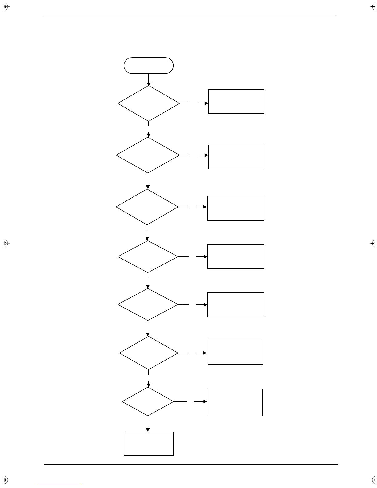
Troubleshooting
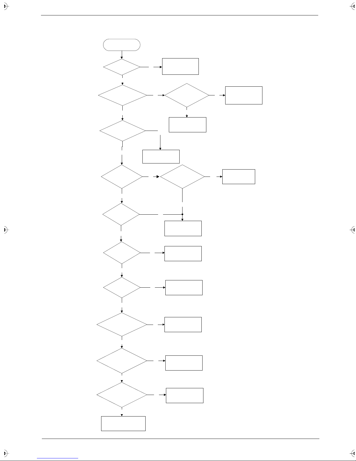
VIDEO CIRCUIT
NO IMAGE
ARE SIGNALS
OUTPUT FROM VIDEO
OUTPUT TERMINAL?
No
ARE SIGNALS
OUTPUT FROM PG2201
pins
17,15,13,11,9,7,3
?
No
ARE SIGNALS
OUTPUT FROM IC2202
pins
35,33,29,28,
?
25,24
No
ARE SIGNALS
IC2202
pins
14,15,16,
?
20,21
Yes
Yes
Yes
No
CHECK SIGNAL
CABLE/ MONITOR
CHECK VIDEO OUTPUT
SECTOR (PG1302/J1307/
J1302/J1306/J1361) OF
RJK PwB
CHECK Q2206/Q2207/
Q2208/Q2209/Q2210/
Q2211/Q2212
CHECK IC1201/IC1101/
IC1601
Yes
+5V AT IC2202
pins
46,34,32,30,27,
(VDD)?
19,11,1
Yes
IS VOLTAGE AT
IC2202 pin
(RESET) H LEVEL?
IS CLOCK IN
IC2202 pin
REPLACE IC2202
Yes
Yes
48
44
?
No
No
No
CHECK POWER
SUPPLY CIRCUIT
CHECK IC1601
CHECK X2201/ R1218
22 Chapter 1
AUDIO CIRCUIT
NO SOUND
IS THERE
AN IMAGE?
Yes
ARE IC1502
pins
8, 9, 15, 20
5V?
Yes
ARE THERE
SIGNALS AT IC1501~4
pins
ARE THERE
SIGNALS AT pins
BASE VOLTAGE
1, 2, 3, 5
Yes
?
13, 16
Yes
IS Q1505
0V?
Yes
?
No
BREAKDOWN OF
No
BREAKDOWN
BEFORE IC1201
ARE IC1506 pin 2 +5V
No
No
IC1201
ARE THERE
SIGNALS AT IC1501~4
pins
No
BREAKDOWN OF
+8V
& pin
1
Yes
BREAKDOWN OF
IC1506
?
26, 27, 28
No
IC1601
No
Yes
CHECK IC1606
OR +8V LINE ETC.
BREAKDOWN OF
IC1501~4
IS Q1506
COLLECTOR
VOLTAGE
-8V?
Yes
IS IC1501~4
VOLTAGE
pin
21
5V?
Yes
IS Q1507, Q1508, Q1501
COLLECTOR VOLTAGE
-8V?
YES
ARE SIGNALS AT
IC1507,IC1508,
IC1511,IC1513
?
pins
1,7
YES
ARE SIGNALS AT
IC1509,
IC1510,IC1512,IC1514
?
pins
1,7
Yes
BREAKDOWN OF
Q3503 OR Q3504
Q1306~Q1311
D1504 OR ZD1307
No
No
No
Q1507,Q1508,Q1501
No
IC1507,IC1508,IC1512,
No
IC1509,IC1510,IC1512,
BREAKDOWN OF
Q1505 OR Q1506
OR D1504
BREAKDOWN OF
IC1501~IC1504
BREAKDOWN OF
BREAKDOWN OF
IC1514
BREAKDOWN OF
IC1514
Chapter 1 23
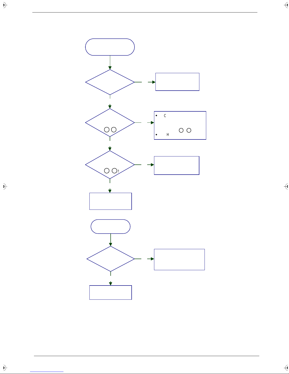
KARAOKE CIRCUIT
(Only available at DVD-5500/DVD-5300 models)
NO MIC SOUND
IS THERE DISC
SOUND?
Yes
ARE
SIGNAL AT IC2401
1 7
?
Yes
ARE
SIGNAL AT IC2404
?
CHECK IC2404,
IC1201, IC1505 ETC.
85
Yes
No
No
No
NO SOUND OUTPUT
CHECK ROUTE
FROM MIC JACK
J1763/1764 TO
IC2401
CHECK IC2401 ETC.
CHECK MIC
VOLUME RV1762,
RV1763 ETC.
3 5
NO ECHO/KEY
CONTROL EFFECT
REMOTE
CONTROL ACTION
OK?
Yes
CHECK IC1201 ETC.
No
CHECK REMOTE
CONTROLLER AND
RECEIVE CONTROL
CIRCUIT ETC.
24 Chapter 1

About System Reset Function
The player can not work normai ly wi th non-s tand ard dis cs. If you encount er the ab normal stat us , plea se press
STOP button once to st op it . If it can’t stop normaily, please press POWER/STANDBY button. If the status is
not changed in about 20 seconds after pressi ng PO WER/ STANDBY button then just press LAST button and
ENTER button concurrently on the front panel to reset the system. After reseting, the system will restart and
change into standby mode (The POWER/STANDBY indicator lights in red color ). Therefore, please press
POWER/STANDBY button agai n to start the system. (Pull out the power cord and plug it again, the restarte d
system will also change into standby state.)
System Utility
How to upgrade the system utility
1. Power on the system and press the OPEN/CLOSE button to open the DVD-ROM tray.
2. Place the version-up CD-R disc into the DVD-ROM.
3. The DVD player will read the CD-R disc and upgrade the system utility version, after about 40 seconds,
the DVD-ROM tray will open auto ma ti cally.
4. Take out the version-up CD-R disc.
5. Pull out the power cord then plug it again.
6. Press the POWER/STANDBY button to rest art the system, while the DVD-ROM tray clos ed, the version
had been upgarded already.
NOTE: If the version of th e system utility in the CD-R di sk is older than original one, then the front display
window will shows ‘No play’.
How to check the system utility version
1. At the power on state, press the POWER/ST ANDBY button and LAST button once in the same ti m e and
then release the POWER/STANDBY button only and st il l press the LAST button continually for m ore than
5 seconds.
2. The front display window will appear the sys tem utility version.
Chapter 1 25

26 Chapter 1

Removal and Replacement
Prelimaries before disassembling machines
This chapter cont ains step-by- step procedures on how to disassemble the DVD system for mainte nance and
troubleshooting.
To disassemble the system, you need the following tools:
Wrist grounding strap and conductive mat for preventing electrostatic discharge
Phillip s s cre w dr iv e r
Tweezers
NOTE: The screws for the different components vary in size. During the disassembly process, group the
screws with the corresponding components to avoid mismatch when putting back the componen ts.
Before You Begin
Before proceedi ng with the disassembly procedure, make sur e that you do the following:
1. Turn off the power to the system and al l peripherals.
2. Unplug the AC adapter and all power and signal cables from the system.
Chapter 2
Chapter 2 27
 Loading...