

Page 1
August, 2001 Training Materials Prepared by: Daniel Newman
CONTENTS... 2001 DLP-1 Chassis Projection Television Information
INSTRUCTOR… Alvie Rodgers C.E.T.
Page 2

DLP-1 Chassis
DLP Basics
Page 3
DLP-1 Chassis DLP Basics
DMD™ Roadmap
SVGA: 848x600; 508, 800 mirrors
XGA: 1024x768 chip with black aperture; 786,432 mirrors
SXGA: 1280x1024; 1,310,720 mirrors
(continued)
Page 0-01
Page 4
DLP-1 Chassis DLP Basics
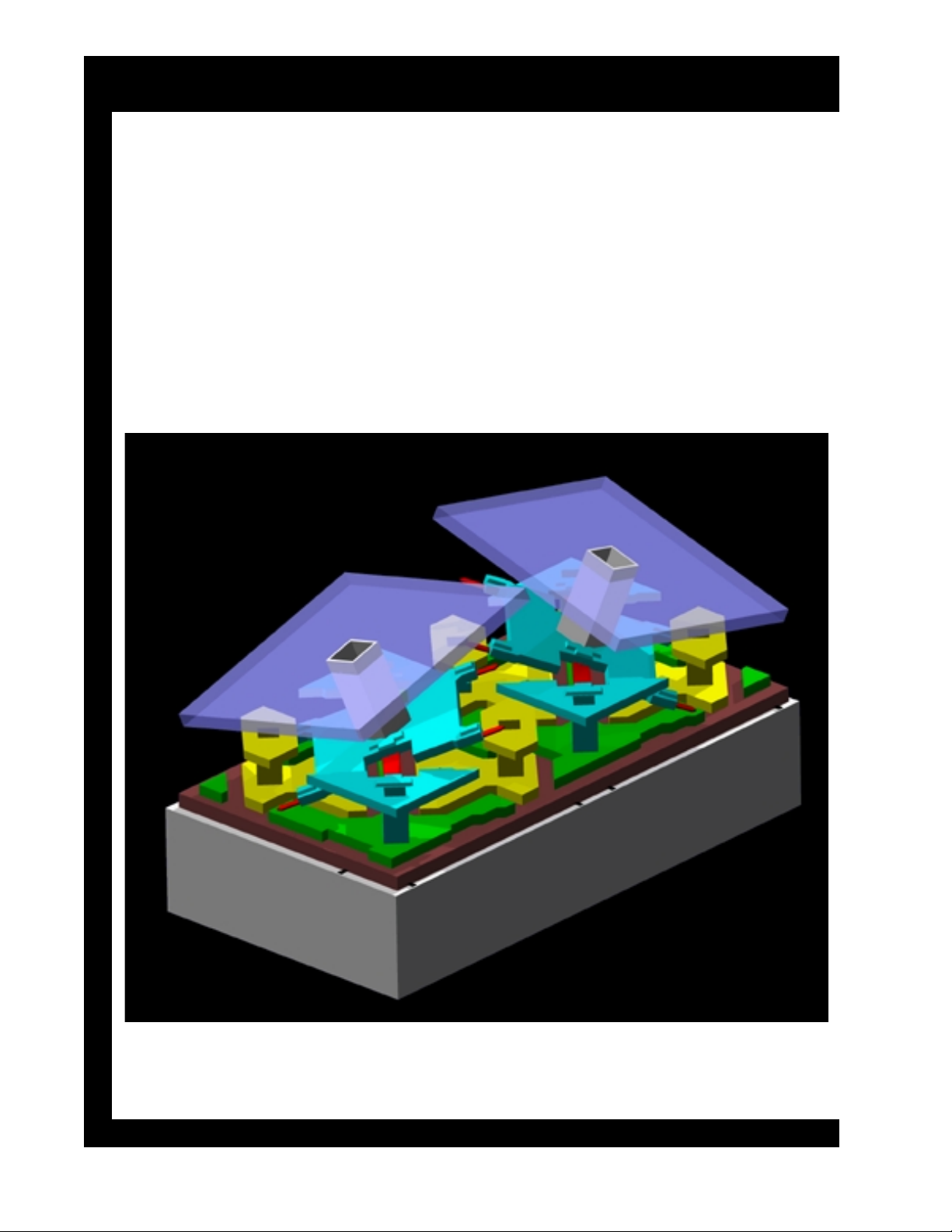
Two Mirrors
The illustration shows a blow up of two mirrors on the DMD, one on
and one off. Light hitting the "on" mirror will reflect through the
projection lens to the screen. Light hitting the off mirror will reflect
to a light absorber. Each mirror is individually controlled and is
totally independent of all other mirrors. Each frame of a movie is
separated into its red, blue, and green components and digitized into
1,310,000 samples for each color. Each mirror in the system is
controlled by one of these samples.
(continued)
Page 0-02
Page 5
DLP-1 Chassis DLP Basics
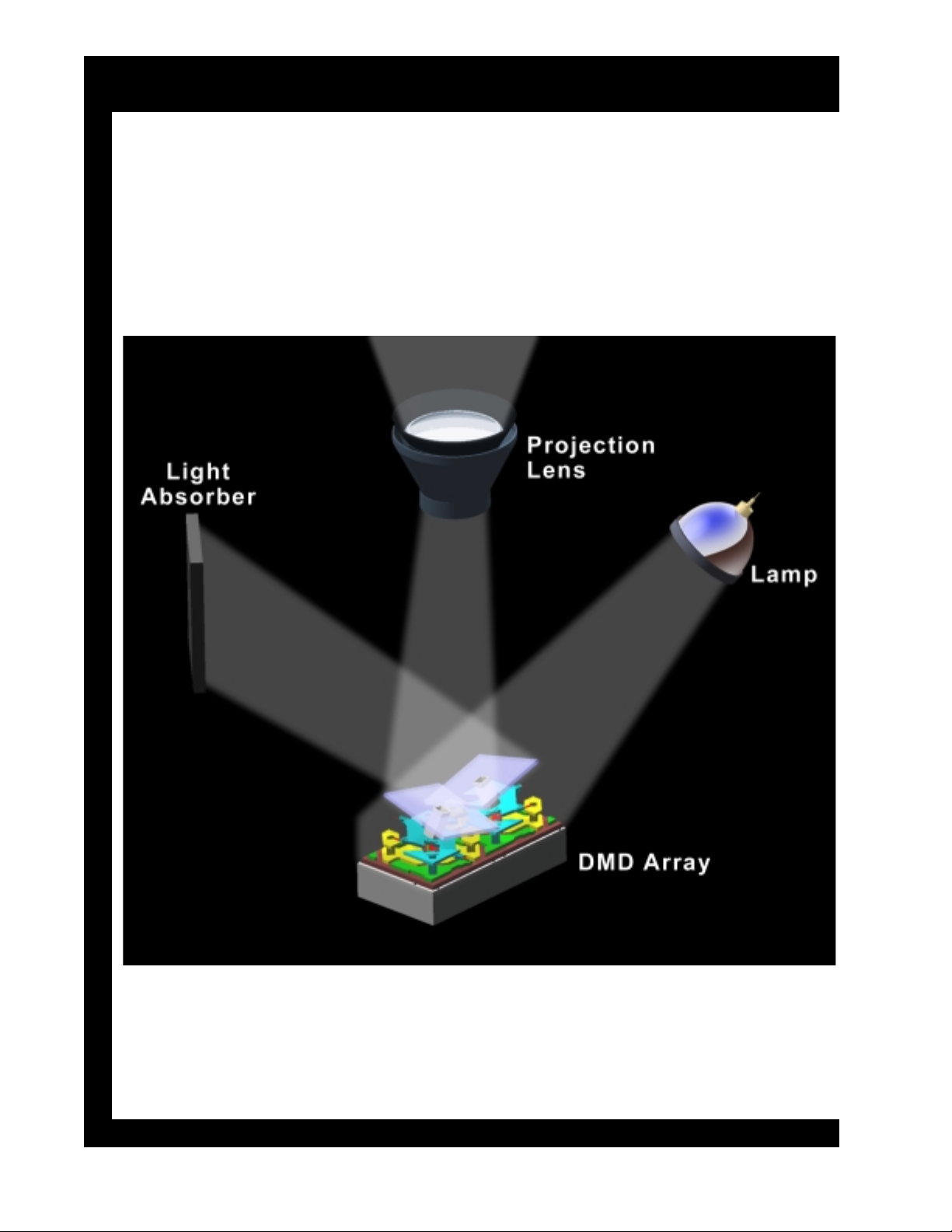
Two Mirrors Wit h Lamp, Projection, Lens, and Light Absorber
The "on" mirror reflects light into the lens and the "off" mirror
reflects light into the light absorber.
(continued)
Page 0-03
Page 6
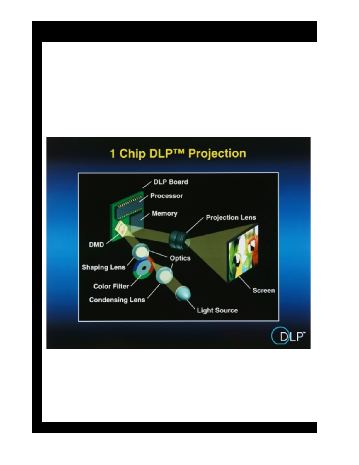
DLP-1 Chassis DLP Basics
1-Chip DLP™ Projection System
White light is forced down onto a color wheel filter. This wheel spins
in sequence with the red, green and blue video signal being sent to
the DMD™. Mirrors are turned on, depending on where and how
much of each color is needed for each TV field. The human visual
system integrates the sequential color and sees a full-color image.
(continued)
Page 0-04
Page 7
DLP-1 Chassis DLP Basics
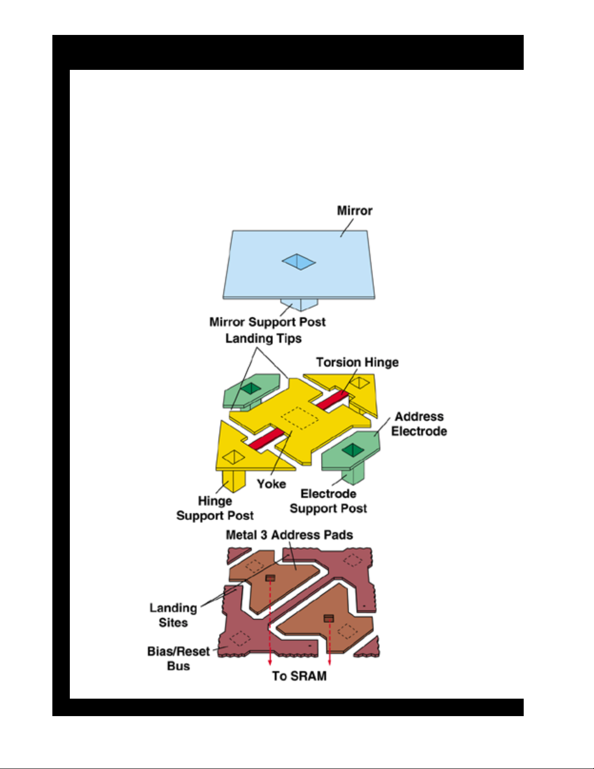
DMD™ Architecture
Exploded view of an individual mirror on a DMD. Each 16 µm
mirror on a DMD consist of these three physical layers and two
"airgap" layers. The airgap layers separate the three physical layers
and allow the mirror to tilt +10 or -10 degrees.
2
(continued)
Page 0-05
Page 8
DLP-1 Chassis DLP Basics
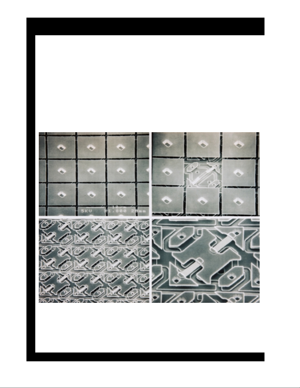
DMD™ with Mirror Removal
The top left view shows nine mirrors. The top right view shows the
central mirror removed to expose the underlying, hidden-hinge
structure. The bottom right shows a close-up view of the mirror
substructure. The mirror post, which connects to the mirror, sits
directly on the center of this underlying surface. Lastly the bottom
left view shows several pixels with the mirror removed.
(continued)
Page 0-06
Page 9
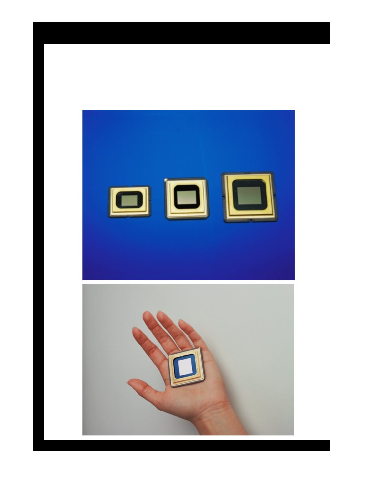
DLP-1 Chassis DLP Basics
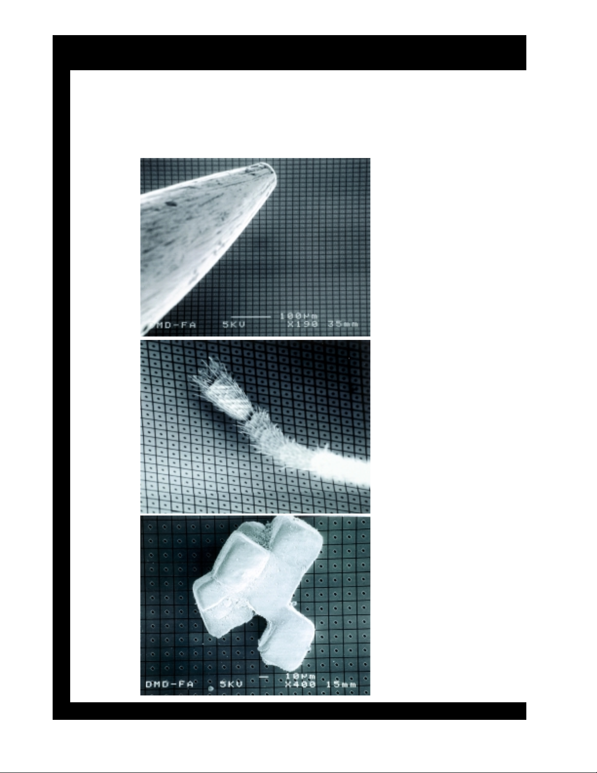
DMD™ Size Comparisons
Micrographic photos of the tip of a pin, an ant’s leg, and one granule
2
of salt on the surface of a DMD. Each mirror is 16 µm
separation between pixels.
with 1 µm
Page 0-07
Page 10

DLP-1 CHASSIS
Front & Rear
Panels
Page 11
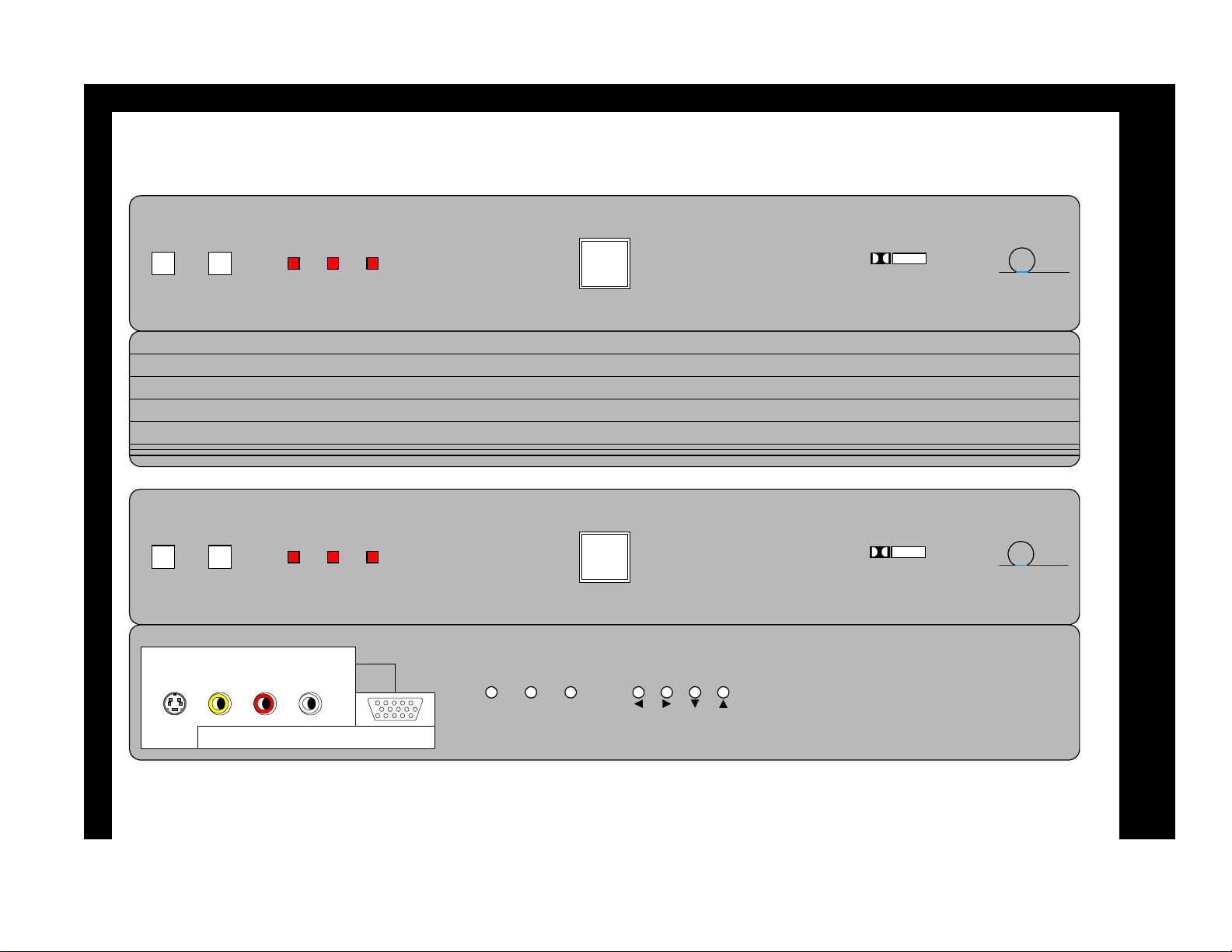
55DM X01W Front Panel
AUDIO/
PC AUDIO
S-VIDEO VIDEO L/(MONO) R
INPUT 2
POWERTEMPLAMP
POWER
HITACHI
DO BLY
DIGITAL
TM
LP
D
A TEXAS INSTRUMENTS TECHNOLOGY
DLP-1 Chassis Controls and Connections
PUSH
POWERTEMPLAMP
INPUT MENU
TV/PC EXIT SELEC T
POWER
VOL- VOL+ CH- CH+
HITACHI
DO BLY
DIGITAL
LP
D
A TEXAS INSTRUMENTS TECHNOLOGY
TM
Page i-01
INPUT 3 PC RG B INPU T 2
(continued)
Page 12
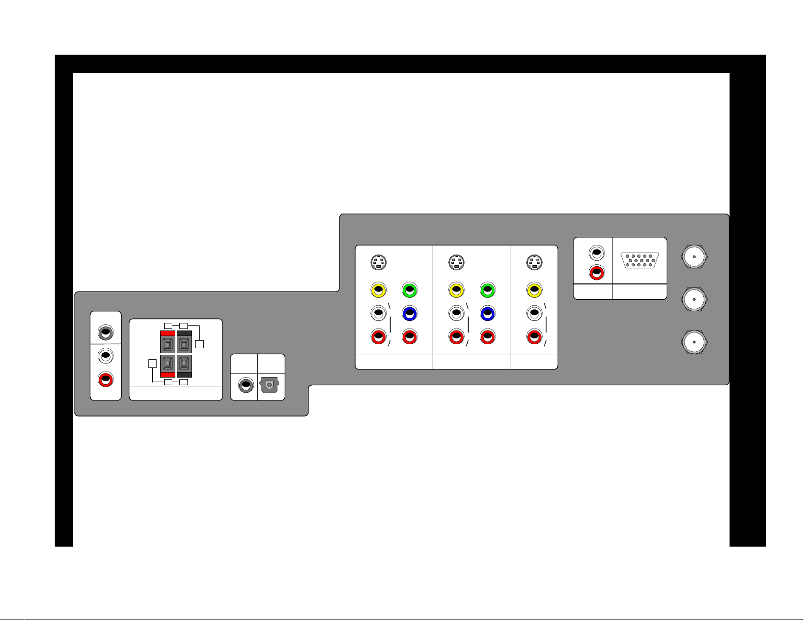
55DM X01W Rear Panel
S-VIDEO
S-VIDEO
S-VIDEO
DLP-1 Chassis Controls and Connections
ANT A
L
Page i-02
R
PC AUDIO
INPUT 1
PC RGB INPUT 1
TO
CONVERTER
ANT B
SUB
WOOFER
L
R
AUDIO
TO HIFI
R
+ -
REAR SPEAKER 8
VIDEO
(MONO)
-+
ONLY
ΩΩΩΩ
L
COAXIAL
OPTICAL
INPUT
INPUT
AUDIO
Y
Pb
L
Pr
R
VIDEO
(MONO)
AUDIO
INPUT 1 INPUT 2
Y
Pb
L
Pr
R
VIDEO
(MONO)
AUDIO
MONITOR
OUT
L
R
(continued)
Page 13
55DMX 01W Rear View
DLP-1 Chassis Controls and Connections
Page i-03
PC RGB INPUT 1
CONVERTER
ANT A
TO
ANT B
S-VIDEO
VIDEO
Y
(MONO)
Pb
SUB
WOOFER
L
R
-+
L
COAXIAL
R
+ -
AUDIO
REAR SPEAKER 8
TO HIFI
OPTICAL
INPUT
INPUT
ΩΩΩΩ
ONLY
L
Pr
R
AUDIO
INPUT 1 INPUT 2
S-VIDEO
S-VIDEO
VIDEO
Y
(MONO)
Pb
L
Pr
R
AUDIO
MONITOR
L
R
VIDEO
PC AUDIO
INPUT 1
(MONO)
L
R
AUDIO
OUT
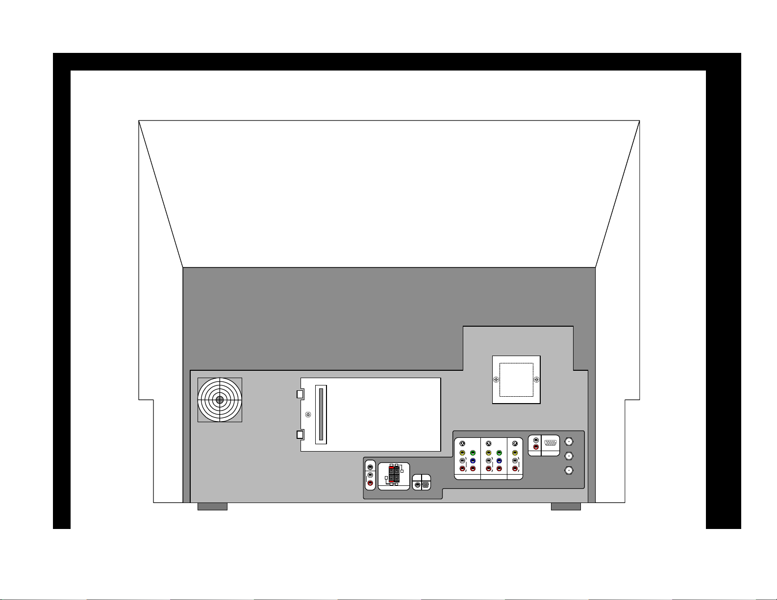
Page 14
55DM X01W PW B Layout
MICON PWBSURROUND PWBPOWER PW B
DSP UNIT
DLP-1 Chassis Controls and Connections
Page i-04
SIGNAL PWB
UY01 UF01
TE R MINA L P WB
2H PWB
Tuner
PWB
U201
U202
Page 15

DLP-1 Chassis
Power Distribution
Page 16

DLP-1 Chassis Power Distribution
POWER PW B
When AC is applied, the Switched Mode Power Supply (A) circuit consisting of I901 and T901 (see Figure 1) will
start producing the following DC voltages: +13V, +18V, -15V, and +42V. When the unit is turned on, the power
relay contacts close, and AC will be applied to the Switched Mode Power Supply (B) circuit consisting of I902 and
T902 (see Figure 2), which will then produce the following DC voltages: +370V, +28V, +12V, and +8V.
POWER PW B
AC
IN
+13V
+18V
I901&T901
SMPS (A)
-15V
To SMP S (B)
+42V
Figure 1 - Switched Mode Power Supply (A)
SMPS (A) (See Figure 1)
+13V
The +13 volt supply is the source for several lower supply voltages:
I954 Fan +12V Regulator IC
I955 Fan +12V Regulator IC
I956 Fan +12V Regulator IC
I951 STBY +5V Regulator IC
I952 BS +2.5V Regulator IC
It is also sent directly out to the SIGNAL PWB via connector PSQ1[3], and to the MICON PWB via connector
PMQ[1], where it is then called STBY +13V.
+18V
The +18 volt supply is the source for several lower supply voltages:
I953 BS +6.5V Regulator IC
I957 AUD +12V Regulator IC
It is also sent directly out to the SIGNAL PWB via connector PSQ1[9].
-15V
The –15 volt supply is the source for the AUD –12V supply regulated by Q9E3.
+42V
The +42 volt supply is the source for the VT+35V supply regulated by Q9F0.
FAN +12V Supply (I954, I955, I956)
The FAN +12V supplies are supplied by the +13V source from T901 and are regulated by I954, I955, and I956,
and then sent out to the Fans via connectors PQF1[2], PQF2[2], and PQF3[2].
PQF1
I95 4
Fan +12V
2
FAN +12V
Fan +12V
I95 1
Stby +5V
I95 2
BS + 2.5 V
I95 3
BS + 6.5 V
I95 7
Aud +12V
Q9E3
-12V
Q9F0
+35V
I95 5
2
PQF2
FAN +12V
PQF3
I95 6
Fan +12V
2
FAN +12V
5
STBY +5V
1
STBY +13V
PMQ
(To MICON PWB)
3
STBY +13V
1
AUD +12V
7
BS +2.5V
9
+18V
11
VT +35V
5
BS +6.5V
PSQ1
(To SIG N AL PW B )
5
BS +6.5V
6
BS +6.5V
1
AUD +12V
3
AUD -12V
PQU2
(To AUDIO PWB)
(continued)
Page 1-01
Page 17

DLP-1 Chassis Power Distribution
STBY +5V Supply (I951)
The STBY +5V supply is supplied by the +13V source from T901 and is regulated by I951 and is sent out to the
MICON PWB via connector PMQ[5].
BS +2.5V Supply (I952)
The BS +2.5V supply is supplied by the +13V source from T901 and is regulated by I952 and is sent out to the
SIGNAL PWB via connector PSQ1[7].
BS +6.5V Supply (I953)
The BS +6.5V supply is supplied by the +18V source from T901 and is regulated by I953 and is sent out to the
SIGNAL PWB via connector PSQ1[5] and the AUDIO PWB via connector PQU2[5,6].
AUD +12V Supply (I957)
The AUD +12V supply is supplied by the +18V source from T901 and is regulated by I957 and is sent out to the
SIGNAL PWB via connector PSQ1[1] and the AUDIO PWB via connector PQU2[1].
AUD -12V Supply (Q9E3)
The AUD -12V supply is supplied by the -15V source from T901 and is regulated by Q9E3 and is sent out to the
AUDIO PWB via connector PQU2[3].
VT +35V Supply (Q9F0)
The VT +35V supply is supplied by the +42V source from T901 and is regulated by Q9F0 and is sent out to the
SIGNAL PWB via connector PSQ1[11].
To SM PS (A)
I902&T902
SMPS (B)
(To Lamp Ballast PWB)
SMPS (B) (See Figure 2)
+28V
The +28 volt supply is sent directly out to the AUDIO PWB via connector PQU1[5,6], where it is then called
A+28V. It is also applied to IA01 which is the Front Audio Output IC.
+12V
The +12 volt supply is the source for several lower supply voltages:
I962 MSC +9V Regulator IC
Q959 3.3V Regulator Transistor
It is also sent directly out to the SIGNAL PWB via connector PSQ1[13] where it is then called +12VB, and out to
the DLP PWB via connector PQD[10] where it is then called DLP +12V.
+28V
IA01
Front Audio
Out
+12V
I962
MSC+9V
Q959
+3.3V
+8V
I959
DLP+5V
I960
MSC+3.3V
1
Lamp +370V
PQL
I961
MSC+5V
POWER PW B
Figure 2 - Switched Mode Power Supply (B)
5
A+28V
6
A+28V
PQU1
(To AUDIO PWB)
13
+12VB
15
+8VB
PSQ1
(To S IGNAL PW B)
8
DLP +3.3V
7
DLP +3.3V
6
DLP +3.3V
6
DLP +12V
9
DLP +5V
PQD
(To DLP PWB)
10
MSC +9V
6
MSC +3.3V
5
MSC +3.3V
4
MSC +3.3V
12
MSC +5V
10
MSC +5V
PBQ2
(To MSC P W B)
(continued)
Page 1-02
Page 18

DLP-1 Chassis Power Distribution
+8V
The +8 volt supply is the source for several lower supply voltages:
I959 DLP +5V Regulator IC
I960 MSC +3.3V Regulator IC
I961 MSC +5V Regulator IC
It is also sent directly out to the SIGNAL PWB via connector PSQ1[15], where it is then called +8VB.
+370 Volt Supply (Unregulated)
The +370V supply is basically raw B+ and sent to the Lamp Ballast PWB via connector PQL[1].
MSC +9V Supply (I962)
The MSC +9V supply is supplied by the +12V source from T902 and is regulated by I962 and is sent out to the
MSC PWB via connector PBQ2[14].
DLP +3.3V Supply (Q959)
The DLP +3.3V supply is supplied by the +12V source from T902 and is regulated by Q959 and is sent out to the
DLP PWB via connector PQD[6,7,8].
DLP +5V Supply (I959)
The DLP +5V supply is supplied by the +8V source from T902 and is regulated by I959 and is sent out to the DLP
PWB via connector PQD[9].
MSC +3.3V Supply (I960)
The MSC +3.3V supply is supplied by the +8V source from T902 and is regulated by I960 and is sent out to the
MSC PWB via connector PBQ2[4,5,6].
MSC +5V Supply (I961)
The MSC +5V supply is supplied by the +8V source from T902 and is regulated by I961 and is sent out to the
MSC PWB via connector PBQ2[10,12].
AUD +9V
STBY +5V
ST BY + 3 .3 V
(To CONTROL PWB)
STBY +5V
ST BY + 3 .3 V
(To REMOTE PWB)
STBY +5V
STBY +13V
(From POWER PWB)
MICON PWB (See Figure 3)
STBY +3.3V Supply (Q029)
The STBY +3.3V supply is supplied by the STBY +5V source on the POWER PWB and is regulated by Q029 and
is used on the MICON PWB. It is also sent out to the REMOTE PWB via connector PMJ[3], the CONTROL
PWB via connector PMR1[5], and the C.W. SENSOR PWB via connector PME[3].
1
3
5
PMR1
1
3
PMJ
5
1
PMQ
Q029
STBY +13V SEL +9V
STBY +5V
+3.3V
+5V1H
ST BY + 3 .3 V
MICON PWB
Figure 3 - MICON PWB
4
STBY +5V
PSM1
(To SIGNAL PWB)
3
ST BY + 3 .3 V
PME
(To C.W. SENSOR PWB)
6
AUD +9V
8
SEL +9V
18
+5V1H
PSM3
(From SIGNAL PW B)
(continued)
Page 1-03
Page 19

DLP-1 Chassis Power Distribution
BS +6.5V
BS +2.5V
+18V
VT +35V
+12VB
+8VB
1
3
5
7
9
11
13
15
PSQ1
2
4
6
8
PSB1
BS + 2 .5 V
VT +35V
+12VB
+8VB
IP0 1
5V1H
IP0 2
5V2H
IP0 3
5V3D
IP0 4
9V1H
IP0 5
9V2H
5V1H
5V2H
5V3D
9V1H
9V2H
Figure 4 - SIGNAL PWB
IP0 6
AUD+9V
IP0 7
SEL+9V
IP0 8
9VFC1H
IP0 9
9VFC2H
IP1 0
12V2H
IP1 1
5VFC
IP1 2
3.3VFC
AUD+9V
SEL+9V
9VFC1H
9VFC2H
12V2H
5VFC
3.3VFC
SIGNAL PWB
(continued)
Page 1-04
AUD +12V
STBY +13V
(From POWER PWB)
(To TUNER PWB)
SIGNAL PWB (See Figure 4)
5V1H Supply (IP01)
The 5V1H is a +5 volt supply which is supplied by the +8VB supply on the POWER PW B, which is then regulated
by IP01. It is made available to the 1H video circuitry on the SIGNAL PWB.
5V2H Supply (IP02)
The 5V2H is a +5 volt supply which is supplied by the +8VB supply on the POWER PW B, which is then regulated
by IP02. It is made available to the 2H video circuitry on the SIGNAL PWB.
5V3D Supply (IP03)
The 5V3D is a +5 volt supply which is supplied by the +8VB supply on the POWER PW B, which is then regulated
by IP03. It is made available to the 3DYC comb filter circuitry on the SIGNAL PWB.
9V1H Supply (IP04)
The 9V1H is a +9 volt supply which is supplied by the +12VB supply on the POWER PWB, which is then
regulated by IP04. It is made available to the 1H video circuitry on the SIGNAL PWB.
9V2H Supply (IP05)
The 9V2H is a +9 volt supply which is supplied by the +12VB supply on the POWER PWB, which is then
regulated by IP05. It is made available to the 2H video circuitry on the SIGNAL PWB.
AUD+9V Supply (IP06)
The AUD+9V is a +9 volt supply which is supplied by the AUD+12V supply on the POWER PWB, which is then
regulated by IP06. It is made available to the audio circuitry on the SIGNAL PWB.
SEL+9V Supply (IP07)
The SEL+9V is a +9 volt supply which is supp lied by the STBY+1 3V supply on the P OWER PW B, which is then
regulated by IP07. It is made available to various circuitry on the SIGNAL PWB.
Page 20

DLP-1 Chassis Power Distribution
9VFC1H Supply (IP08)
The 9VFC1H is a +9 volt supply which is supplied b y the STBY+13V supply on the POW ER PWB, which is then
regulated by IP08. It is made available to the Flex Converter (1H portion) on the SIGNAL PWB.
9VFC2H Supply (IP09)
The 9VFC2H is a +9 volt supply which is supplied b y the STBY+13V supply on the POW ER PWB, which is then
regulated by IP09. It is made available to the Flex Converter (2H portion) on the SIGNAL PWB.
12V2H Supply (IP10)
The 12V2H is a +12 volt supply which is supplied by the +18V supply on the POWER PWB, which is then
regulated by IP10. It is made available to the 2H video circuitry on the SIGNAL PWB.
5VFC Supply (IP11)
The 5VFC is a +5 volt suppl y which is supplied b y the BS+6.5V supp ly on the POWE R PWB, which is then
regulated by IP11. It is made available to the Flex Converter circuitry on the SIGNAL PWB.
3.3VFC Supply (IP12)
The 3.3VFC is a +3.3 volt supply which is supplied b y the 5VFC supply on the SIGNAL PW B, which is then
regulated by IP12. It is made available to the Flex Converter circuitry on the SIGNAL PWB.
VT+35V
(From SIGNAL PW B)
TUNER PWB (See Figure 5)
+9V Supply (I201)
This +9V is a +9 volt supply which is supplied by the +12VB supply on the POWER PWB, which is then
regulated by I201. It is made available to the two tuners on the TUNER PWB.
+9V Supply (I202)
This +9V is a +9 volt supply which is supplied by the +12VB supply on the POWER PWB, which is then
regulated by I202. It is made available to the Antenna Switch Box via connector EBA [3].
+5V Supply (I203)
This +5V is a +5 volt supply which is supplied by the +8VB supp ly on the POWER PW B, which is then regulated
by I203. It is made available to the two tuners on the TUNER PWB.
+12VB
+12VB
+8VB
2
4
6
8
PSB1
TUNER PWB
I201
+9V Reg
I202
+9V Reg
I203
+5V Reg
Figure 5 - TUNER PWB
1
U201
9
Main
2
Tuner
3
10
U202
7
Sub
Tuner
11
3
EBA
(To An t S w B o x )
(continued)
Page 1-05
Page 21

DLP-1 Chassis Power Distribution
AUDIO PWB (See Figure 6)
AUD+5V Supply (IS13)
The AUD+5V is a +5 volt supply which is supplied by the BS +6.5V supply on the POWER PWB, which is then
regulated by IS13. It is made available to the audio circuitry on the AUDIO PWB and also to the DSP (Digital
Surround Processor) Module via connector PMU1[1].
AUD+9V AUD+9V
(From SIGNAL PW B)
AUD+12V
AUD-12V
BS+6.5V
BS+6.5V
(From POWER PWB)
A+28V
A+28V
(From POWER PWB)
1
PSU1
1
3
5
6
PQU2
5
6
PQU1
IS1 3
AUD+5V
IS1 5
Center Out
IS1 6
Rear Out
AUDIO PWB
Figure 6 - AUDIO PWB
AUD+12V
AUD-12V
AUD+5V
9
8
PMU3
(To DSP Module)
1
PMU1
(To DSP Module)
Page 1-06
Page 22

DLP 55DMX01W POWER ON/OFF CIRCUIT DIAGRAM (Microprocessor Side)
STBY 3.3V
PWR
CONTROL PWB
STBY 5V
HR01 IR IN
REMOTE PWB
MICON PWB
8
PMR1
5
PMJ
Q014
7
KEY IN
PWR On/Off
45
DATA
1
I001
µ
µprocessor
STBY 13V
Q050
OFF
Q049
ON
OFF
53
ON
Q052
ON
OFF
Q051
Q020
Temp Alarm
Fan Alarm
Lamp Cover
CDBRK
OFF
ON
Power1
OFF
ON
Power2
Power2
7
To
POWER
PWB
8
9
PMQ
PAGE 01-07
Page 23

DLP 55DMX01W POWER ON/OFF CIRCUIT DIAGRAM (Microprocessor Side)
AF 29V
Power 1
From
MICON
PWB
Power2
Power2
STBY 5V
Power 1
7
8
9
PMQ
S901
TV S
OFF
ON
TV V Power1
BS Power
STBY 18V
Q9E4
STBY 5V
AC
5
2
I957
Aud +12V
1
Q9F7
S902
3
4
STBY 13V
Q9F6
STBY 5V
5
2
Audio +12V
I955
Fan +12V
1
STBY 13V
STBY 18V
Q9E3
3
4
1
5
5
Fan +12V
2
I953
BS 6.5V
3
I954
1
PSQ1
PQU2
2
4
Audio (Front) 29V
1
1
To Signal PWB
To Surround PWB
FAN2 +12V
3
4
FAN1 +12V
BS +6.5V
PAGE 01-08
AC to
SMPS-B
STBY 13V
Q9E2
1
5
I952
BS 2.5V
3
2
4
BS +2.5V
Page 24

DLP-1 Chassis
Video Circuit
Explanation
Page 25

DLP-1 Chassis Video Circuit Explanation
(See Figure 1 on Page 2-04)
TERMINAL PWB
The TERMINAL PWB is where most of the video inputs come into and go out of. The main components on this
PWB are I301 (A/V Select IC) and IT01 (PiP 3-Line Comb Filter).
I301 (A/V Select)
This IC receives the following video inputs:
TV1 Main Tuner video (NTSC)
TV2 Sub Tuner video (NTSC)
V1 Composite video from AUX VIDEO INPUT 1
V1(Y) Luminance portion of S-Video from AUX VIDEO INPUT 1
V1(C) Chrominance portion of S-Video from AUX VIDEO INPUT 1
Comp 1 Y Luminance portion of Component Video from AUX VIDEO INPUT 1
V2 Composite video from AUX VIDEO INPUT 2
V2(Y) Luminance portion of S-Video from AUX VIDEO INPUT 2
V2(C) Chrominance portion of S-Video from AUX VIDEO INPUT 2
Comp 2 Y Luminance portion of Component Video from AUX VIDEO INPUT 2
V3 Composite video from AUX VIDEO INPUT 3 via the front panel connector PTR
V3(Y) Luminance portion of S-Video from AUX VIDEO INPUT 3 via the front panel connector PTR
V3(C) Chrominance portion of S-Video from AUX VIDEO INPUT 3 via the front panel connector PTR
Y In1 Luminance portion of Sub Video from IT01 PiP Comb Filter
C In1 Chrominance portion of Sub Video from IT01 PiP Comb Filter
This IC also provides the following outputs:
V Out1 Sub Video out which is sent to IT01 PiP Comb Filter
V/Y Out2 Main Video out or Luminance portion of main S-video which is sent to the SIGNAL PWB
C Out2 Chrominance portion of main S-video which is sent to the SIGNAL PWB
Mon Out V Composite video sent to MONITOR OUTPUT
Mon Out (Y) Luminance portion of S-Video sent to MONITOR OUT
Mon Out (C) Chrominance portion of S-Video sent to MONITOR OUT
IT01 (PiP 3-Line Comb Filter)
This IC receives Sub Video from I301 on pin 3. It outputs Sub Y on pin 25 and Sub C on pin 23.
TUNER PWB
The TUNER PWB is where the two tuners are located. The main components on this PWB are U101 (Main
Tuner) and U102 (Sub Tuner).
U101 (Main Tuner)
This non-repairable unit outputs Main Tuner NTSC Video to connector PSB5[4], where it goes to the SIGNAL
PWB, then to the TERMINAL PWB on connector PST1[4].
U102 (Sub Tuner)
This non-repairable unit outputs Sub Tuner NTSC Video to connector PSB5[10], where it goes to the SIGNAL
PWB, then to the TERMINAL PWB on connector PST1[10].
SIGNAL PWB
The SIGNAL PWB receives and processes the following signals:
Sub (Y / C)
Main (V or Y / C)
Component 1 (Y/Cr/Cb or Y/Pr/Pb)
Component 2 (Y/Cr/Cb or Y/Pr/Pb)
(continued)
Page 2-01
Page 26

DLP-1 Chassis Video Circuit Explanation
Sub Video
The Sub Y and Sub C signals are applied to IY02, which basically converts the Sub C (chrominance) signal into
two color difference signals, which are called Sub R-Y or Sub Cr and Sub B-Y or Sub Cb. It then outputs all three
signals to IX01, which is the Y/CR/CB Select IC.
Main Video
The Main video signal, whether it’s V or Y / C, is applied to UY01 3DYC Comb Filter. If the Main video wasn’t
Y / C when it came in, it will be when it comes out. Main Y and Main C si gnals are applied to IY01 which
basically converts the Main C (chrominance) signal into two color difference signals, which are called Main R-Y
or Main Cr and Main B-Y or Main Cb. It then outputs all three signals to IX01 which is the Y/CR/CB Select IC.
Component 1
The component 1 video signal can be any of the approved ATSC or NTSC formats; 480i, 480p, 1080i, etc. This
signal is inserted directly into IX01 which is the Y/CR/CB Select IC.
Component 2
The component 2 video signal can be any of the approved ATSC or NTSC formats; 480i, 480p, 1080i, etc. This
signal is inserted directly into IX01 which is the Y/CR/CB Select IC.
IX01 (Y/CR/CB Select IC)
This IC receives four different inputs, Sub (Y/Cr/Cb), Main (Y/Cr/Cb), Component 1 (Y/Cr/Cb or Y/Pr/Pb), and
Component 2 (Y/Cr/Cb or Y/Pr/Pb). Note that since both the Sub and Main signals ultimately come from NTSC
sources, it is not possible for them to be Y/Pr/Pb. IX01 provides two outputs; Main and Sub, which are then
applied to UF01, which is the Picture in Picture / Flex Converter Unit.
UF01 (Picture in Picture / Flex Converter Unit)
The Picture in Picture / Flex Converter Unit receives two inputs, Main and Sub, and provides one combined or
processed output. If any PiP request is made by the customer, it will combine/split the two signals into one signal
as long as both of the input signals contain the same original format; i.e. 480i, 480p, etc. It will also up-convert the
frequency (base H) of incoming 15.734 KHz to approximately 2.86H or 45 KHz or 720p.
2H VIDEO PWB
The 2H VIDEO PWB receives and processes the following signals:
PiP/Flex Converter Output (2H Y/Cr/Cb)
Main Output from IX01
Rear PC RGB
Front PC RGB
PiP/Flex Converter Output
As previously mentioned, the PiP/Flex Converter output sends out a processed signal (PiP information added) that
is (possibly) as high as 45 KHz located on connector PSH1[9,11,13]. Also found on that same connector [2,4,6] is
a set of signals that mirror the main input to the PiP/Flex Converter. This set of signals will be used in the case of
a non-480i (480p, 1080i, etc.) input via the component 1 or component 2 inputs, and is applied to I501.
2H Y/Cr/Cb
The Y portion of the 2H Y/Cr/Cb is sent directly to I501. The 2H Cr/Cb is sent to two places; I502 and the
YCBCR/YIQ converter circuitry.
YCRCB/YIQ Converter
The purpose of the YCRCB/YIQ Converter circuitry is to phase shift the color information contained in the
YCRCB signal by 33 degrees. This is done so that the auto-flesh tone or auto-color circuitry in IK01 RGB
processor can function properly. The auto-color function only works with YIQ signals, so the output from the Flex
Converter must be converted (phase shifted) if the original signal was NTSC. The Cr/Cb signal can also be ter med
U/V. The phase shifted signal is then applied to I502.
(continued)
Page 2-02
Page 27

DLP-1 Chassis Video Circuit Explanation
I502 (NTSC/Other Select IC)
I502 receives two sets of red and blue color difference information; one in the form of Cr/Cb or U/V and the other
in the form of I/Q. Selection is made by the sensing of NTSC or non-NTSC. If NTSC is sensed, then the I/Q input
would be selected. The output is sent to I501.
I501 (15.75 KHz / Other Select IC)
This IC receives two sets of signals; one directly from the output of IX01 (main out) via connector PSH1[2,4,6]
and the other from I502 NTSC/Other Select IC. In the case of an input signal other than 480i, or 15.75 KHz, the
Flex Converter does not need to up-convert the signal, so this signal is sent directly to I501 as this will typically be
a high(er) definition source such as 1080i. The other signal available to I501 will be the processed signal from
I502 via the Flex Converter and phase shifted if necessary. Selection is made by the sensing of a non-15.75 KHz
input signal. The output is sent to IK01 RGB Processor in the form of Y/I/Q or Y/U/V.
IK01 (RGB Processor)
This IC receives two sets of inputs; one from the output of I501 which would be video, and the other from the
MICOM PWB in the form of OSD R, OSD G, and OSD B. It processes and combines the two signals (when
applicable) and outputs main RGB to IC02, which is the TV / PC Select IC.
IC01 (Front / Rear PC Select)
This IC receives two sets of PC RGB signals; one from the front panel via connector PHR[1,3,5] and the other
from the TERMINAL PWB via connector PHT[1,3,5]. The IC then selects whichever one the customer selects via
the main control menu. The output is sent to IC02, which is the TV / PC Select IC.
IC02 (TV / PC Select IC)
This IC receives two sets of signals; one which is main video from the RGB processor IC IK01, and the other from
the Front / Rear PC Select IC IC01. The output is sent to the MSC PWB in the form of RGB.
MSC PWB
This PWB is located physically on the Optical Engine Assembly. Nothing is known about what goes on inside this
module, although there appears to be an output which consists of a flat 50 pin cable which includes signals called
A0-LVTTL, A1-LVTTL, B2-LVTTL, C3-LVTTL, etc., which may possibly stand for Low-Voltage-TransistorTransistor-Logic, since there is a 3.3 volt power source sent to this PWB.
DLP PWB
This PWB is also located physically on the Optical Engine Assembly. Nothing is known about what goes on
inside this module either, although this is where the actual Micro-Mirror-Device is located.
(continued)
Page 2-03
Page 28

DLP
PWB
1
1
50
to to
50
153
R
29
1
8
R
3
2
1
RGB
153
50 Pin
LVTTL
MSC - DLP
MSC
OPTICAL ENGINE ASSY
PWB
PHC
B
G
26
23
IC02
TV/PC
Select
3
5
10
12
B
G
9
6
2H VIDEO P W B
IC01
PC Select
Front/Rear
8
7
5
4
RGB
153
PHT
PHR
Figure 1
UF01
SIGNAL PWB
IX0 1
191817
Unit
PiP/FC
38
36
34
(Y) SUB O U T
(Cr/Pr) SUB OUT
(Cb/Pb ) S U B O U T
Y/CB/CR Select
COMP 1 (Cr/Pr)
MAIN Cb (NTSC)
SUB Cr (NTSC)
SUB Cb (NTSC)
SUB Y (NTSC)
5
7
9
37
47
48IY02
SUB
NTSC
6
40
MAIN Y (NTSC)
63
15
17
19 MAIN Cr (NTSC)
37
47
48IY01
MAIN
NTSC
6
40
534
46
(Cr/Pr) MAIN O UT
COMP 1 (Cb/Pb)
COMP 1 (Y)
59
61
PFC1
50
48
(Y) MAIN O U T
(Cb/Pb ) M AIN O U T
COMP 2 (Cr/Pr)
COMP 2 (Cb/Pb)
COMP 2 (Y)
53
55
57
2
(Y) MAIN O U T
8
162018
6
4
9
2H Y
(Cr/Pr) MAIN O UT
(Cb/Pb ) M AIN O U T
9
1
14
PFC2
13
11
PSH1
2H CR
2H CB
YCBCR/YIQ
CONVERTER
I
Q
1
14
11
16
I502
Select
NTSC/Other
3
5
434142
16
11
R OUT
B OUT
IK01
RGB
G OUT
Processor
DLP -1 Chassis Video Block Diagram
Sub Y
Sub C
UY01
8
PiP
IT01
3-Line
3
25
23
6
Main Y
Main C
9
7
11
13
3DYC
COMP 1 (Cr/Pr)
COMP 1 (Cb/Pb)
COMP 1 (Y)
COMP 2 (Cr/Pr)
COMP 2 (Cb/Pb)
COMP 2 (Y)
2
4
PST2
26
28
30
19
21
23
PST1
I501
5
Select
15.75 Khz/Other
6
3
Y
535152 U/Q
V/I
OSDB
OSDG
OSDR
39
37
38
PWB
From
MICON
49
51
53V Out1
Y In1
C In1
56
Y Out1
44
58
C Out1
47
C Out2
V/Y Out2
TERMINAL PWB
I301
TV1
4
4
Main
U101 Tuner
TV2
63
10
PST1
10
PSB5
PiP
U102 Tuner
V1
V1(C)
V1(Y)
156017
Video 1
19
S-Video 1 (C)
S-Video 1 (Y)
30 Comp 1 Y
Comp Video 1 (Y)
Comp Video 1 (Cr/Pr)
TUNER PWB
A/V Select
Comp Video 1 (Cb/Pb)
Video 2
V2(C)
V2(Y)
V2
8
12
10
S-Video 2 (C)
S-Video 2 (Y)
3 Comp 2 Y
Comp Video 2 (Y)
Comp Video 2 (Cr/Pr)
Comp Video 2 (Cb/Pb)
Video 3
V3
V3(Y)
V3(C)
24
26
22
RGB
3
5
10
PTR
S-Video 3 (C)
S-Video 3 (Y)
5
3
1
PHR
PC Front
Monito r O ut (V id eo )
Page 2-04
Mon O u t (C )
Mon O u t (Y)
Mon Out V
37
39
41
PC Rear
Monito r O ut (S -V ide o ) (C )
Monito r O ut (S -V ide o ) (Y )
FRONT PANEL
Page 2-04
Page 29

DLP-1 Chassis
Audio Circuit
Explanation
Page 30

DLP-1 Chassis Audio Circuit Explanation
(See Figure 1 on Page 3-04)
TERMINAL PWB
The TERMINAL PWB is where the analog audio inputs come into. The main components on this PWB are I301
(A/V Select IC) and I302 (Audio Switch IC).
I301 (A/V Select)
This IC receives the following audio inputs:
TV1(L) Main Tuner audio (Left)
TV1(R) Main Tuner audio (Right)
V1(L) Left Channel audio from AUX VIDEO INPUT 1
V1(R) Right Channel audio from AUX VIDEO INPUT 1
V2(L) Left Channel audio from AUX VIDEO INPUT 2
V2(R) Right Channel audio from AUX VIDEO INPUT 2
V3(L) Left Channel audio from AUX VIDEO INPUT 3 via Audio Switch IC I302
V3(R) Right Channel audio from AUX VIDEO INPUT 3 via Audio Switch IC I302
This IC also provides the following outputs:
SEL (L) Selected Left Channel Audio which is sent to the SURROUND PWB
SEL (R) Selected Right Channel Audio which is sent to the SURROUND PWB
Mon Out (L) Selected Left Channel Audio which is sent to MONITOR OUTPUT
Mon Out (R) Selected Right Channe l Audio whic h i s sent to MONITOR OUTP UT
I302 (Audio Switch IC)
This IC receives two sets of left and right audio input; one set from the front panel which is Aux Video 3 / PC, and
one set from the rear PC audio input. It has one set of left and right audio output which is sent to the V3( L) and
(R) inputs on I301. It is controlled by the PC F/R signal.
SURROUND PWB
The SURROUND PWB receives and processes the following signals:
SEL (L) and (R)
Digital Audio via Optical Input
Digital Audio via Coaxial Input
The SURROUND PWB processes and outputs the following signals:
Front Audio (L) and (R)
Rear Audio (L) and (R)
Center Channel
Subwoofer (LFE)
HiFi Outputs (L) and (R)
SURROUND PWB INPUTS
SEL (L) and (R)
The SEL (L) and (R) signals are the selected output from I301 (A/V Select IC) and are input to IS19 (Perfect
Volume IC) via connector PSU1[12,13]. The output of IS19 is then divided and sent to two places; IS03 (Front
Audio Control IC), and to the DSP (Digital Signal Processor) module via connector PMU2[1,3].
Digital Audio Input (Optical)
The Digital Audio Input (optical) is a fiber optic connection which is coupled to a transducer which converts the
digital audio data via light pulses to a n electrical signal, in fact very similar in operation to a n Infra-Red remote
receiver. It is widely regarded as inferior to coaxial digital connections. Also known as an "optical" or "Toslink"
connection. After this signal has been converted, it is sent to IS17 (Digital Audio Selector IC).
(continued)
Page 3-01
Page 31

DLP-1 Chassis Audio Circuit Explanation
Digital Audio Input (Coaxial)
An RCA type cable with a central conductor surrounded by an insulating material, around which is another tubular
conductor (known as the screen or shield). In digital audio, the coaxial cable yields better results than Toslink
(optical) due t o i ts highe r qua l it y co nnec t io n and wider si gn al ba nd widt h. This signal is s ent t hro u gh a b uf fer sta ge
IS18 (Coaxial Buffer IC) before going into IS17 (Digital Audio Selector IC).
IS17 (Digital Audio Selector IC)
This IC receives both the optical and coaxial sources of digital audio and selects which one is sent to the DSP
(Digital Signal Processor) module as an input.
DSP (Digital Signal Processor) Module
This module is a separate PWB that is mounted piggyback on the SURROUND PWB. It receives Left and Right
audio in from the Perfect Volume IC and creates the following outputs; Front Right, Front Left, Rear Right, Rear
Left, Center Channel, and Subwoofer. It also is capable of receiving and processing a digital audio input signal,
via either coaxial or optical inputs.
SURROUND PWB OUTPUTS
Front Audio (L) and (R)
The Front Audio left and right consist of the following components; IS03 (Front Audio Control IC), IS05 (Front
Audio Graphic Equalizer IC), and IA01 (Front Audio Output IC).
IS03 (Front Audio Control IC)
This IC receives two sets of left and right audio; one set is the non-DSP processed left and right input from I301
(A/V Select IC) via IS19 (Perfect Volume IC), and the other set which has been processed by the DSP module.
The output of IS03 is sent to IS05 (Front Audio Graphic Equalizer IC).
IS05 (Front Audio Graphic Equalizer IC)
This IC receives the Front Audio left and right from IS03 (Front Audio Control IC) and provides the user with five
frequency ranges or bands which he can manipulate by approximately 12db in both the plus and minus directions.
The frequency bands are 60 Hz, 125 Hz, 1 KHz, 3 KHz, and 10 KHz. The outputs from this IC are sent to two
places; IA01 (Front Audio Output IC) via connector PQU3[2,4], and also to the HiFi Output jacks located on the
rear of the SURROUND PWB.
IA01 (Front Audio Output IC)
This IC is not located on the SUR ROUND PWB but on the P OWER PWB as previously disc ussed on page 1-02.
It is a standard TA8200AH audio output IC. The outputs from this IC are sent to the two front speakers via
connectors PL[2] and PR[2].
Rear Audio (L) and (R)
The Rear Audio left and right consist of the following components; IS11 (Rear Audio Control IC), and IS16 (Rear
Audio Output IC).
IS11 (Rear Audio Control IC)
This IC receives Rear Audio left and right which has been processed by the DSP module. The outputs of IS11 are
sent to IS16 (Rear Audio Graphic Equalizer IC).
IS16 (Rear Audio Output IC)
This IC is also a standard TA8200AH audio output IC. It outputs speaker level audio to the Rear Speaker jacks
located on the rear of the SURROUND PWB.
(continued)
Page 3-02
Page 32

DLP-1 Chassis Audio Circuit Explanation
Center Channel Audio (Monaural)
The Center Channel Audio consists of the following components; IS08 (Center/Subwoofer Audio Control IC),
IS10 (Center Channel Audio Graphic Equalizer IC), and IS15 (Center Channel Audio Output IC).
IS08 (Center Channel / Subwoofer Audio Control IC)
This IC receives Center Channel Audio which has been processed by the DSP module. The Center Channel Audio
output of IS08 is sent to IS10 (Center Channel Audio Graphic Equalizer IC).
IS10 (Center Channel Audio Graphic Equalizer IC)
This IC receives the Center Channel Audio from IS08 (Center Channel / Subwoofer Audio Control IC) and
provides the user with five frequency ranges or bands which he can manipulate by approximately 12db in both the
plus and minus directions. The frequency bands are 60 Hz, 125 Hz, 1 KHz, 3 KHz, and 10 KHz. The Center
Channel Audio output from this IC is sent to IS15 (Center Channel Audio Output IC).
IS15 (Center Channel Audio Output IC)
This IC is also a standard TA8200AH audio output IC. It outputs speaker level audio to the center speaker via
connector PCL[2].
Subwoofer Audio (LFE)
The Subwoofer Audio (Low Frequency Effects) consists of IS08 (Center/Subwoofer Audio Control IC).
IS08 (Center Channel / Subwoofer Audio Control IC)
This IC receives Subwoofer (LFE) Audio which has been processed by the DSP module. The Subwoofer (LFE)
audio output of IS08 is sent to the Subwoofer connector on the rear of the SURROUND PWB.
(continued)
Page 3-03
Page 33

L
R
C
2
2
PL
PR
2
PCL
Figure 1
Out(FL)
Out(FR)
Front
POWER PW B
4In(FL)
Out(FL)
In(FL)
In(FR)
Out(FL)
Out(FR)
In(L)
In(R)
IA01
IS05
IS03
Audio Out
Front
Graphic EQ
Control
Front Audio
In(FR)
2
PQU3
Out(FR)
In(FL)
In(FR)
IS15
Center
In(C) Out (C)
In(C) Out(C)
Out(C)
Out(SW)
In(C)
In(SW)
Audio Out
IS10
Center
Graphic EQ
IS08
Aud i o
Control
Center/SW
IS01
DAC4
Out(SL)
Out(SR)
Rear
IS16
In(SL )
In(SR )
Out(SL)
Out(SR)
In(SL )
In(SR )
Audio Out
IS11
Control
Rear Audio
DLP -1 Chassis Audio Block Diagram
3
1
PMU2
Out(L)
Out(R)
IS19
Perfect
Volume
In(L)
In(R)
SURROUND PW B
12
13
PSU1
28
27
PST2
SEL (L)
SEL (R)
BUSY
DIR ERR
ERR MUTE
ZRNSSN
SOSISCK
1
8106
4
12214
I001
Processor
µ
µµ
µ
RESETN
PUM1
In(L)
In(R)
BUSY
DIR ERR
ERR MUTE
ZRNSSN
SOSISCK
MICON PWB
13
9
8123
10
11
I301
TV1(L)
TV1(R)
V1(L)
V1(R)
V2(L)
V3(L)
V2(R)
V3(R)
A/V Select
Mon O ut (L )
Mon Out(R)
6
5
CSI
RESETN
1
2
346
Out(FL)
5
Out(C)
Out(FR)
Out(SW)
PMU1
REQUEST
PMU3
Out(SL)
Out(SR)
In(Digita l)
DSP MODULE
7
PMU1
3
PMU4
IS17
Selector
Digital Audio
I302
Audio SW
In1(L)
In1(R )
In2(R )
Out(L)
Out(R)
In2(L)
IS18
2
1
PST1PSB5
2
1
16
15
PST2
Optical Input
CoAx Buffer
Surround Left Speaker Out
Surround Right Speaker Out
HiFi Out (Left)
CoAxial Input
Sub Woofer Out
HiFi Out (Right)
Monito r O ut (L e f t)
Main
U101 Tun er
Video 1 (Left)
TUNER PWB
Video 2 (Left)
Video 1 (Right)
Video 3 / PC (Left)
Video 2 (Right)
Video 3 / PC (Right)
Rear PC (Left)
Rear PC (Right)
Front Panel
Monito r O ut (Right)
Page 3-04
Digital
TERMINAL PWB
Audio In
SURROUND PW B
Page 3-04
Page 34

DLP-1 Chassis
System Control
Explanation
Page 35

DLP-1 Chassis System Control Explanation
In the DLP-1 Chassis (
Figure 10
), as in many other Hitachi products, System Control starts
at the microprocessor IC, I001. The following signals are generated b y the microprocessor
IC; (
see Figure 1
Clock/Data
)
Clock
M Enable
Data
0Clock/0Data
1Clock/1Data (also called SCL1 and SDA1)
2Clock/2Data (also called SCL2 and SDA2)
M Enable - Main Tuner Enable
P Enable - PiP Tuner Enable
FC Enable - Flex Converter Enable
P Enable
I00 1
MicroProcessor
FC E n a b le
0Clock
0Data
1Clock (SCL1)
1Data (SDA1)
MSC Enable - MultiScan Converter Enable
MSC Enable
2Clock (SCL2)
2Data (SDA2)
Figure 1 - System Control signals
Clock/Data
Clock and data are fed to the following circuits: Main tuner, PiP tuner, Flex Converter, and
the MSC (MultiScan Converter) PWB. Additional ly, each of these circuits also requires an
Enable signal whenever that circui t activates. (
see Figures 2, 3, 4, and 5
) Also, note that
0Clock/0Data is only sent to the MSC PWB.
Main
Tuner
M Enable
P Enable
FC E nab le
MSC Enable
I001
MicroProcessor
Figure 2 - Clock, Data, and Main Enable
M Enable
FC
Unit
P Enable
FC E nab le
MSC Enable
I001
MicroProcessor
Clock
Data
0Clock
0Data
1Clock (SCL1)
1Data (SDA1)
2Clock (SCL2)
2Data (SDA2)
Clock
Data
0Clock
0Data
1Clock (SCL1)
1Data (SDA1)
2Clock (SCL2)
2Data (SDA2)
Figure 4 - Clock, Data, and Flex Converter Enable
Clock
Clock
Data
0Clock
0Data
1Clock (SCL1)
1Data (SDA1)
2Clock (SCL2)
2Data (SDA2)
Data
0Clock
0Data
1Clock (SCL1)
1Data (SDA1 )
2Clock (SCL2)
2Data (SDA2 )
M Enable
PiP
Tuner
P Enable
FC Enable
MSC Enable
I001
MicroProcessor
Figure 3 - Clock, Data, and PiP Enable
M Enable
P Enable
MSC
Unit
Figure 5 - Clock, Data, 0Clock, 0Data, and
FC Enable
MSC Enable
I001
MicroProcesso r
MultiScan Converter Enable
(continued)
Page 4-01
Page 36

DLP-1 Chassis System Control Explanation
1Clock/1Data (SCL1/SDA1)
The clock and data 1 lines are fed to the following: I002 E2PROM, I004 DAC1, I003
DAC2, I017 DAC3, IS11 Rear Audio Control, and I301 A/V Select. (see
Figure 6
of DAC’s (Digital to Analog Converter) are basically configured as fan-out IC’s for the
microprocessor. (
see Figure 7
). This allows the microprocessor IC to remain as a standard
dual inline 64 pin configuration as far as the actual IC manufacturing process is concerned.
Each DAC can communicate up to nine (9) separate functions back to the main
microprocessor. Including the three DAC’s, the clock/data 1 line communicates to 30
different devices.
EEPROM
M Enable
Clock
Data
DAC1
P Enable
I00 1
MicroProcessor
FC En a b le
0Clock
0Data
1Clock (SCL1)
1Data (SDA1)
DAC2
DAC3
MSC Enable
2Clock (SCL2)
2Data (SDA2)
Rear Audio
A/V Select
Figure 6 - 1Clock, 1Data, (SCL1, SDA1)
I004
DAC 1
YUV 1 DET
YUV 2 DET
COMP SEL
CHECK 2
LED FAN
LED LAMP
LED PWR
LAMP ENA
CDBRK
I003
DAC 2
IR D E T
YV DET
0RES
MTS
F MONO
ANT
PWRG
SAP DET
ST DET
I017
DAC 3
). The use
I002
I004
I003
I017
IS1 1
I301
LAMP MISS
FAN ALARM
15K/OTHER
PC/OTHER
LAMP CTR
LAMP LIT
FAN ON
TEMP AL AR M
FILTER COVER
Figure 7 - DAC 1, DAC 2, and DAC 3 pin outs
(continued)
Page 4-02
Page 37

DLP-1 Chassis System Control Explanation
2Clock/2Data (SCL2/SDA2)
The clock and data 2 lines are fed to the following: UY01 3DYC Comb Filter, IT01 PiP
3Line Comb Filter, IX01 Y/Cb/Cr Select, I018 DAC5, IS05 Front Graphic EQ, IY01 Main
NTSC processor, IL01 Main Sync processor, IK01 RGB processor, IS01 DAC4, IS08
Center/Subwoofer Control, IY02 Sub NTSC processor, IL02 Sub Sync processor, DLP
PWB, IS03 Front Audio control, and IS10 Center Graphic EQ. (see
Figure 8
DAC’s (Digital to Analog Converter) are again configured as fan-out IC’s for the
microprocessor. (
see Figure 9
). Although it appears to be more loaded down than the
SCL1/SDA1 line, the clock/data 2 line communicates to 31 different devices.
). The use of
M Enable
P Enable
FC En able
MSC Enable
I00 1
MicroProcessor
UY01
3DYC
IT01
PiP 3Line
Clock
Data
0Clock
0Data
1Clock (SCL1)
1Data (SDA1)
2Clock (SCL2)
2Data (SDA2)
IX01
Y/Cb/Cr
I018
DAC5
IS05
Fr Graphic
Figure 8 - 2Clock, 2Data, (SCL2, SDA2)
IY01
Main NTSC
IL01
Main Sync
IK01
RGB Proc.
IS01
DAC4
IS08
C/SW
IY02
Sub NTSC
IL02
Sub Sync
DLP PWB
IS03
Fr Audio
IS10
C Graphic
IS0 1
DAC 4
SW SEL 1
DSP CSI
OPTI/COAX SEL
R SP OF
C SP OFF
F SP OFF
SW SEL 2
P VOL
DSP REQ
I018
DAC 5
Figure 9 - DAC 4 and DAC 5 pin outs
COLOR WH
TEST 2
COMP 1 CHK
COMP 2 CHK
POW MA SK
POW +
TEST 9
TEST 3
TEST 4
(continued)
Page 4-03
Page 38

DLP-1 Chassis System Control Explanation
SCL2
SDA2
2
1
PSU1
SCL2
SDA2
IL02
IL01
IX01
UY01
3DYC
Y/Cb/Cr
IY02
IY01
Sub NTSC
Main NTS C
Sub Sync
Main S y n c
IS10
IS08
DAC1
IS05
Frnt Graphic EQ
C/SW Audio Cont.
I003
IS11
Cntr Graphic EQ
Rear Audio Cont.
19
18
PUM1
SCL1
SDA1
I002
I004
EEPROM
1Data (SDA1)
1Clock (SCL1)
I001
DAC2
IS01
IS03
DAC4
Frnt Audio Cont.
Surround PWB
8
6
11
10
PSM1
SCL1
SDA1
SCL2
SDA2
I017
DAC3
I018
DAC5
SCL1
SCL2
SDA1
SDA2
24
25
22
23
I30 1
IT01
PiP 3Line
A/V Select
SCL2
8
PST2
IK01
Terminal PWB
2Data (SDA2)
2Clock (SCL2)
Engine
Optical
Assem bly
Signal PWB
SDA2
9
PSH2
RGB Processor
2H Video P WB
Micon PWB
DLP-1 Chassis System Control Block Diagram
MicroProcessor
Data
DLP PWB
Clock
P Enable
16
M Enable
141219
PMB1
FC Enab le
2
3
1
PSM4
UF01
U201
U202
Main Tuner
PiP Tuner
Tuner PWB
Flex Converter
(pa rt of) Sig n a l P WB
0Data
0Clock
MSC Enable
SCL2
643
2
7
SDA2
12
14
PMC
PMD1
12
14
PMD1
SCL2
SDA2
6
4
3
Data
Clock
0Data
Figure 10 - System Control Block Diagram
2
7
0Clock
MSC Enable
Page 4-04
MSC PWB
PMC
Page 39

DLP-1 Chassis
Troubleshooting
Page 40

19.0 TROUBLE SHOOTING FLOW CHARTS
NO PICTURE 1
Is TV picture OK?
NG
OK/PC NG
(*1)
From INCORRECT COLOR
Check the waveform
at pin 1,3,5 of IC02
NG NG
Check the waveform
at pin 3,6,9 of IC01
NG
Check the
waveform at pin
1,4,7 <2,5,8>
of IC01
NG
Check the
waveform at pin
1,3,5 of
PHR <PHT>
NG
OK OK
OK
QC08, QC09,
QC10
Check the waveform
at pin 3,6 of IC03
Check the
waveform at
pin16,21,
<15,20>
of IC01
OK
NG
OK
IC01
Check the
waveform at pin 7,8
of PHR <PHT>
OK
NG
EHR, JM02
OK
DC03, DC04, DC05
<DC08, DC09, DC10>
<EHT, J304>
< > :PC in rear
JM02: Control PWB
J304: Terminal PWB
IC02, IC03
IC01
DC01, DC02
<DC06, DC07>
Check the waveform
at pin 1,3,5 of PHC
NG NG
2H PWB (A)
OK OK
Check the waveform
at pin 7,9 of PHC
2H PWB (B)
TV; H,V sync
EHR, JM02
<EHT, J304>
MSC unit
DLP unit
Optical Engine
2H PWB
118
Page 41

19.0 TROUBLE SHOOTING FLOW CHARTS
NO PICTURE 2
2H PWB (A)
Is waveform at
pin 8,10,12 of
IC02 normal?
NO
Is waveform at
pin 41,42,43 of
IK01 normal?
NO
Does on-screen
display appear?
YES
Is waveform at
pin 53 of IK04
normal?
NO
Is waveform at
pin 6 of I501
normal?
YES
YES
NO
YES
YES
IC02
QK12, QK13,
QK14
IK01, Q524, Q525, Q526
I001 (MICON PWB)
Q506
Is waveform at
pin 24 of IK04
normal?
NO
Is waveform at
pin 16,17 of PSH1
normal?
YES
YES
IK01
Q522, D501
2H PWB (C)
SIGNAL PWB (A)
NO
RF, composite, or
NO
NO
Is input signal
480i component?
YES
Is waveform at
pin 9 of I501
normal?
NO
Is waveform at
pin 9 of PSH1
normal?
YES
YES
NO
UF01
I501
Q507
2H PWB
119
Page 42

19.0 TROUBLE SHOOTING FLOW CHARTS
NO PICTURE 3
SIGNAL PWB (A)
Is waveform at
pin 3,[17] of PFC1
normal?
NO
Is waveform at
pin E of QX08
normal?
NO
Is input signal
RF or Composite?
YES
Is waveform at
pin 15,[5] of IX01
normal?
NO
Is waveform at
pin 40 of IY01 [IY02]
normal?
YES
YES
UF01
QX35, QX36, QX37, QX38
[QX45, QX46, QX47,QX48]
NO
YES YES
Is waveform at
pin E of QY15
[QY13] normal?
NO
YES
IY01,QY12
[IY02, QY09]
Is waveform at
pin E of QY16
[QY14] normal?
YES
QY15, [QY13]
[ ]: SUB PICTURE
SIGNAL PWB (C)
Is waveform at
pin 5,[3] of I005
normal?
YES
Is waveform at
pin 24 of I001
normal?
NO
NO
Q017-Q019, D026
[Q0F1-Q0F3, D0F1]
I005
(*2)
From INCORRECT COLOR
SIGNAL PWB (B)
NO
Is waveform at
pin 11 of UY01 [7 of
PST2] normal?
NO
Is waveform at
pin 60, [63] of I301
normal?
NO
U201,Q201
[U202,Q206]
YES
UY01, QY02, QY20
[QY17, QY19]
YES
I301,Q304,QY16
[Q302,IT01,QY14,QT05-QT07,QT08-QT11]
TERMINAL PWB
NO
TUNER PWB
120
SIGNAL PWB
YES
Is waveform at
pin 2 of I003
normal?
YES
IX01, QX08, [QX22]
I003, I001
NO
Q016, D038
MICON PWB
Page 43

19.0 TROUBLE SHOOTING FLOW CHARTS
NO PICTURE 4
2H PWB (C)
SIGNAL PWB (C)
Is waveform at
pin 8 of I501
normal?
NO
Is waveform at
pin 2 of PSH1
normal?
NO
Is waveform at
pin E of QX08
normal?
NO
Is waveform at
pin 55,<<53>> of
IX01 normal?
NO
YES
YES
YES
YES
I501
Q501
2H PWB
QX09-QX12,QX59
[QX23,QX24,QX60]
Is waveform
at pin E of QY25
<<QY29>> normal?
NO
YES
[ ] : SUB PICTURE
<< >>: COMPONENT 2
Is waveform at
pin 2 of I015
<<I016>> normal?
YES
NO
I015
<<I016>>
QX01,QX56,QY22
<<QX04,QX57,QY26>>
Is waveform
at pin E of QY22
<<QY26>> normal?
NO
YES
QY25,
<<QY29>>
SIGNAL PWB
121
Is waveform at
pin 22 of I001
normal?
YES
Is waveform at
pin 1,<<2>> of
I004 normal?
YES
IX01,QX08,[QX22]
I004,I001
NO
I005, Q046
NO
Q036,Q037
<<Q038,Q039>>
MICON PWB
Page 44

19.0 TROUBLE SHOOTING FLOW CHARTS
2H PWB (B)
TV; H,V sync
Is waveform at
pin 2,5 of IC03
normal?
NO
Is waveform at
pin15,23 of IL01
normal?
NO
Is input signal
RF, composite, or
480i component?
YES
Is waveform at
pin 1,2 of IL01,[IL02]
normal?
YES
YES
NO
YES
IC03
2H PWB
IL03
NO PICTURE 5
[ ]: SUB PICTURE
Is waveform at
pin 3,4,10,11 of
IL01 normal?
YES
IL01
Is waveform at
pin 21 of IL01,
[IL02] normal?
NO
Is waveform at
pin E of QX10,
[QX24] normal?
YES
YES
IL01,[IL02]
QL01-QL03
[QL04-QL06]
NO
Is waveform at
pin 8 of IY01,[IY02]
normal?
NO
Is waveform at
pin 3 of IY03,[IY04]
normal?
NO
Is input signal
RF or Composite?
YES
Is waveform at
pin 7 of IY03,[IY04]
normal?
NO
YES
YES
NO
YES
IL01,[IL02]
IY01,[IY02]
IY03,[IY04]
Is waveform at
pin 5 of IY03
[IY04] normal?
NO
YES
Is waveform at
pin E of QX08
[QX22] normal?
NO
Is waveform at
pin 6,7 of PFC2
normal?
NO
Is waveform at
pin 7,8,14,15 of
PFC1 normal?
NO
IY03
[IY04]
YES
YES
YES
QX09,QX10,QX59
[QX23,QX24,QX60]
IL03
UF01
Is waveform at
pin 13,22 of IL01,
[IL02] normal?
NO
IL03
YES
IL01
[IL02]
NO
Is waveform at
pin E of QX08,
[QX22] normal?
NO
YES
QX09,QX10
[QX23,QX24]
SIGNAL PWB
Is waveform
at pin 11 of UY01
[pin 7 of PST2]
normal?
NO
YES
UY01,QY02,QY03
SIGNAL PWB (B)
NO
SIGNAL PWB (C)
[QY18,QY19]
122
Page 45

19.0 TROUBLE SHOOTING FLOW CHARTS
INCORRECT COLOR
Is waveform at
pin 1,3,5 of PHC
normal?
NO
Is input signal
PC SIGNAL?
NO
Is waveform at
pin 52,53 of IK01
normal?
NO
Is waveform at
pin 3,5 of I501
normal?
NO
YES
YES
YES
YES
MSC Unit
DLP Unit
Optical Engine
(*1)
To NO PICTURE
QK12-QK14,
IC02
Q504,Q505,
IK01
2H PWB
[ ] : SUB PICTURE
<< >>: COMPONENT 2
Is input signal
RF, composite, or
480i component?
NO
Is waveform at
pin 46,48,[34,36] of
IX01 normal?
NO
IX01,QX02,QX03,
<<QX05,QX06>>
YES
Q502,Q503,
YES
QX14-QX16,
QX18-QX20
(*2)
To NO PICTURE
Is waveform at
PFC2 normal?
Is waveform at
pin 4,5,[18,19] of
PFC1 normal?
Is waveform at
pin 46,48,[34,36] of
Is waveform at
pin 6 of IY01 [IY02]
Is waveform at
NO
pin 18,20 of
NO
NO
IX01 normal?
NO
normal?
NO
pin 7 of UY01
normal?
YES
YES
YES
YES
YES
UF01
QX14,QX18,
QX39-QX44,
[QX28,QX32],
[QX49-QX54]
IX01,QY10,QY11
[QY07,QY08]
IY01,QY01,QY04,
QY05,QY06,DY01
Is waveform at
pin 3,5 of I502
normal?
NO
Is input signal RF
or Composite?
NO
Is waveform at
pin 1,14 of I502
normal?
NO
Q508,Q509
YES
YES
YES
I501,Q520,
Q521
I502
Is waveform at
pin 11,16 of I502
normal?
NO
Q508-Q513,
Q518,Q519
YES
I502
2H PWB
SIGNAL PWB
123
Page 46

19.0 TROUBLE SHOOTING FLOW CHARTS
SNOW NOISE
MAIN PICTURE
Reception
Impossible with
Snow Noise
Is there output of
PLL (clock,data,
enable) of I001?
I001
SUB PICTURE
Reception
Impossible with
Snow Noise
Is there output of
PLL (clock,data,
enable) of I001?
NO
NO
YES
YES
Is there voltage
applied (9V,5V,33V)
to U201?
NO
I201,I203,D201,
Q9F1,Q9F2
Is there voltage
applied (9V,5V,33V)
to U202?
NO
YES
YES
U201
U202
I001
I201,I203,D201,
Q9F1,Q9F2
124
Page 47

19.0 TROUBLE SHOOTING FLOW CHARTS
No OSD
Is there
LC oscilation
at pin(47) and
(48) of
I001 ?
Yes
Is there
OSD R, G, B
sibnals at pin
(37), (38), (39) of
I001 ?
No
check
Q005, Q006
No
Yes
check
L003, I001
check
Q0F5, Q007
Q013
125
Page 48

19.0 TROUBLE SHOOTING FLOW CHARTS
No CCD
Is there
Video Y signal
at pin(28) and (30) of
I001 ?
Yes
check
I001
Picture is not blocked by TV Rating/Movie Rating
Main Picture is not blocked
Is there
Video Y signal
at pin(28) of
I001 ?
No
No
check
Q021, Q031
check
Q021
Yes
check
I001
Sub Picture is not blocked
Is there
Video Y signal
at pin(30) of
I001 ?
Yes
check
I001
No
check
Q031
126
 Loading...